Embed Size (px)
Citation preview
ELECTRONICS’ 2007 19 – 21 September, Sozopol, BULGARIA
THE NEW EXCITING AND CHALLENGING REQUIREMENTS TO THE AUTOMOTIVE SUPPLIERS OF SI AND MODULES
Anelia Pergoot, Emil Gueorguiev Saramov
AMI Semiconductor BG, Nikola Vaptzarov str 53,1407 Sofia, Bulgaria, +35929399060, [email protected]
This paper gives a comprehensive overview of the new requirements for the electronics used in the automotive industry. It’s mainly focused on the electronics for engine management, oil control and sensor interface. The challenges for the automotive suppliers are in various professional domains; starting from increasing demands towards the physical limits of operational temperature and ending with clear and straightforward demands towards the management system of the suppliers. This paper is a result of yearlong work of various groups in AMI Semiconductor, number 4 of automotive ASIC’s suppliers in the world.
Keywords: ASIC, ASSP, SoC, EMC, ESD, automotive electronics
1. INTRODUCTION In the 80’s telecom was leading the development of electronics and setting-up
criteria, requirements and technical standards. It was the most globally distributed and used in the normal life electronics. With the increasing competition in the telecom new paradigm’s as reliability, quality systems and standards were created. In the early 90ties the automotive electronics took over the leading role. With the volumes of more than 70M vehicles per year, constantly increasing requirements for human safety and comfort, it became the industry that stretches the limits of technology, production and delivery processes in a way no other industry does it yet. Automotive industry represents 3% of the European gross domestic product and 8% of the EU government’s revenue. It’s the largest R&D investor in Europe with 20% of total R&D and constitutes a major driver for the development of new technologies and innovations.
Being one of the biggest suppliers of ASIC’s to this industry, AMIS carries out intensive research and development work to be able to meet and surpass the increasing demands of the automotive customers.
2. ELECTRONICS UNDER THE HOOD – HIGHER OPERATING TEMPERATURE Si technology is mostly used in computing devices operating at temperatures that
in the worst case are varying between –20 and +85°C . The limits of Si technology and standard packages were tested up-to 125°C and with guarantees in terms of a life time of 10 to 25 years. Many known physical mechanisms are temperature dependent like junction leakages, oxide breakdown, bonding reliability. These parameters are getting worse with increasing temperature while others like hot carrier are getting better. For a long time 125°C maximum junction temperature was sufficient to cover all applications in a car. Increasing the complexity and electronics under the hood and
ELECTRONICS’ 2007 19 – 21 September, Sozopol, BULGARIA
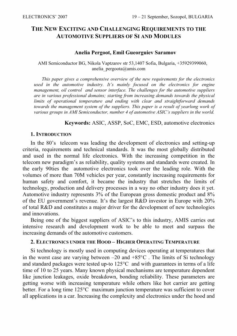
near the engine is setting new temperature target of 170°C junction temperature. In figure 1 are shown the modules where electronics is operating in a higher- temperature environment.
Fig. 1 High temperature electronics in the car
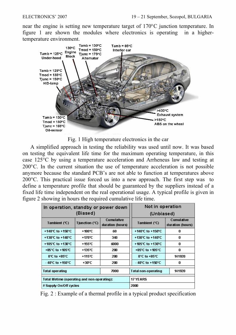
A simplified approach in testing the reliability was used until now. It was based on testing the equivalent life time for the maximum operating temperature, in this case 125°C by using a temperature acceleration and Arrheneus law and testing at 200°C. In the current situation the use of temperature acceleration is not possible anymore because the standard PCB’s are not able to function at temperatures above 200°C. This practical issue forced us into a new approach. The first step was to define a temperature profile that should be guaranteed by the suppliers instead of a fixed life time independent on the real operational usage. A typical profile is given in figure 2 showing in hours the required cumulative life time.
Fig. 2 : Example of a thermal profile in a typical product specification
ELECTRONICS’ 2007 19 – 21 September, Sozopol, BULGARIA
The approach to guarantee these hours has also changed. One starts to test until failure occurs in a way to be able by constructive analysis to understand what type of failure mode leads to breakdown of the component in the Si or in the package.
High temperature in this paper is considered junction temperature above 150°C. As critical at high temperature are considered the following items: junction
leakage in bipolar and DMOS transistors, gate oxide intrinsic life time, Negative Biased Temperature instability of the threshold of MOS transistors (NBTI), Electromigration, Latch-up current, ESD protections, component models used for device simulations, bonding reliability, package stability. The investigation, characterization and improvement of all these elements are subject of yearlong programs of the companies. In this paper an overview of two main items will be given, package and bonding reliability, and hot spot simulation for optimization of the design and layout.
2.1. Package and bonding reliability Package and bonding is recognized as an important limiting factor for HT-
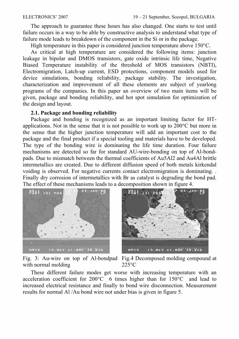
applications. Not in the sense that it is not possible to work up to 200°C but more in the sense that the higher junction temperature will add an important cost to the package and the final product if a special tooling and materials have to be developed. The type of the bonding wire is dominating the life time duration. Four failure mechanisms are detected so far for standard AU-wire-bonding on top of Al-bond-pads. Due to mismatch between the thermal coefficients of Au5Al2 and Au4Al brittle intermetallics are created. Due to different diffusion speed of both metals kirkendal voiding is observed. For negative currents contact electromigration is dominating. . Finally dry corrosion of intermetallics with Br as catalyst is degrading the bond pad. The effect of these mechanisms leads to a decomposition shown in figure 4.
Fig. 3: Au-wire on top of Al-bondpad with normal molding
Fig.4 Decomposed molding compound at 225°C
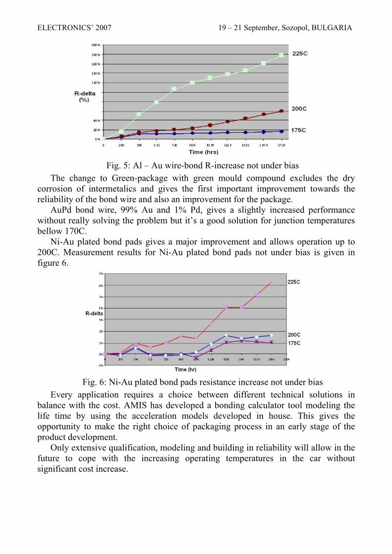
These different failure modes get worse with increasing temperature with an acceleration coefficient for 200°C 6 times higher than for 150°C and lead to increased electrical resistance and finally to bond wire disconnection. Measurement results for normal Al /Au bond wire not under bias is given in figure 5.
ELECTRONICS’ 2007 19 – 21 September, Sozopol, BULGARIA
Fig. 5: Al – Au wire-bond R-increase not under bias
The change to Green-package with green mould compound excludes the dry corrosion of intermetalics and gives the first important improvement towards the reliability of the bond wire and also an improvement for the package.
AuPd bond wire, 99% Au and 1% Pd, gives a slightly increased performance without really solving the problem but it’s a good solution for junction temperatures bellow 170C.
Ni-Au plated bond pads gives a major improvement and allows operation up to 200C. Measurement results for Ni-Au plated bond pads not under bias is given in figure 6.
Fig. 6: Ni-Au plated bond pads resistance increase not under bias
Every application requires a choice between different technical solutions in balance with the cost. AMIS has developed a bonding calculator tool modeling the life time by using the acceleration models developed in house. This gives the opportunity to make the right choice of packaging process in an early stage of the product development.
Only extensive qualification, modeling and building in reliability will allow in the future to cope with the increasing operating temperatures in the car without significant cost increase.
ELECTRONICS’ 2007 19 – 21 September, Sozopol, BULGARIA
2.2. Optimization for hot spots in design In case of important sources of power like drivers, the junction temperature is not
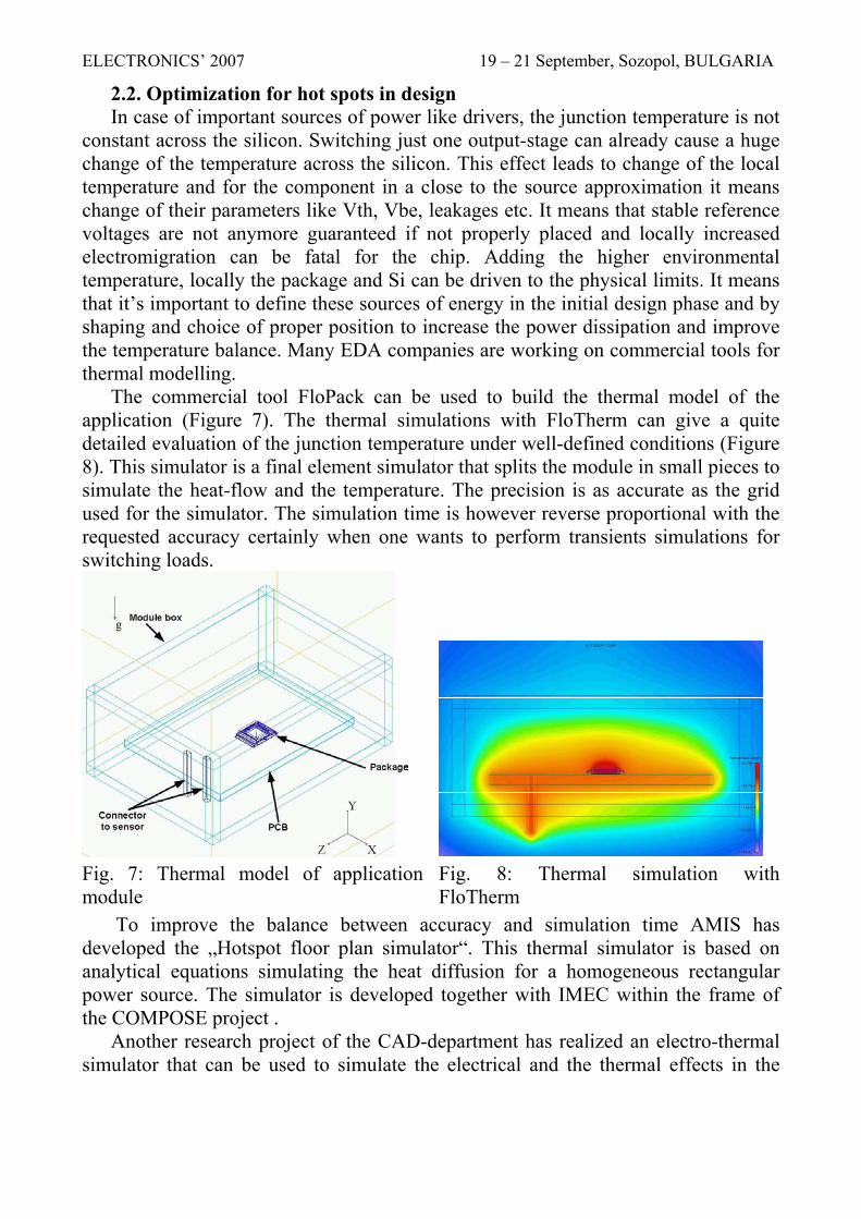
constant across the silicon. Switching just one output-stage can already cause a huge change of the temperature across the silicon. This effect leads to change of the local temperature and for the component in a close to the source approximation it means change of their parameters like Vth, Vbe, leakages etc. It means that stable reference voltages are not anymore guaranteed if not properly placed and locally increased electromigration can be fatal for the chip. Adding the higher environmental temperature, locally the package and Si can be driven to the physical limits. It means that it’s important to define these sources of energy in the initial design phase and by shaping and choice of proper position to increase the power dissipation and improve the temperature balance. Many EDA companies are working on commercial tools for thermal modelling.
The commercial tool FloPack can be used to build the thermal model of the application (Figure 7). The thermal simulations with FloTherm can give a quite detailed evaluation of the junction temperature under well-defined conditions (Figure 8). This simulator is a final element simulator that splits the module in small pieces to simulate the heat-flow and the temperature. The precision is as accurate as the grid used for the simulator. The simulation time is however reverse proportional with the requested accuracy certainly when one wants to perform transients simulations for switching loads.
Fig. 7: Thermal model of application module
Fig. 8: Thermal simulation with FloTherm
To improve the balance between accuracy and simulation time AMIS has developed the „Hotspot floor plan simulator“. This thermal simulator is based on analytical equations simulating the heat diffusion for a homogeneous rectangular power source. The simulator is developed together with IMEC within the frame of the COMPOSE project .
Another research project of the CAD-department has realized an electro-thermal simulator that can be used to simulate the electrical and the thermal effects in the
ELECTRONICS’ 2007 19 – 21 September, Sozopol, BULGARIA
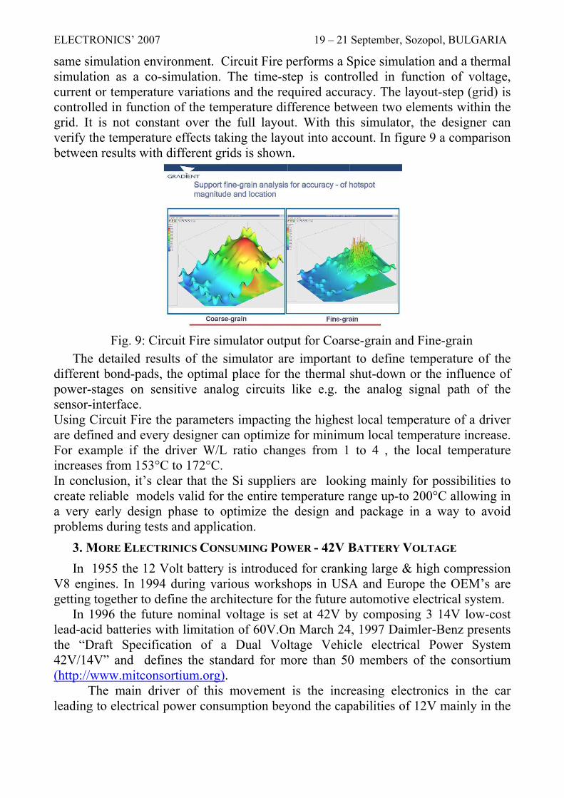
same simulation environment. Circuit Fire performs a Spice simulation and a thermal simulation as a co-simulation. The time-step is controlled in function of voltage, current or temperature variations and the required accuracy. The layout-step (grid) is controlled in function of the temperature difference between two elements within the grid. It is not constant over the full layout. With this simulator, the designer can verify the temperature effects taking the layout into account. In figure 9 a comparison between results with different grids is shown.
Fig. 9: Circuit Fire simulator output for Coarse-grain and Fine-grain
The detailed results of the simulator are important to define temperature of the different bond-pads, the optimal place for the thermal shut-down or the influence of power-stages on sensitive analog circuits like e.g. the analog signal path of the sensor-interface. Using Circuit Fire the parameters impacting the highest local temperature of a driver are defined and every designer can optimize for minimum local temperature increase. For example if the driver W/L ratio changes from 1 to 4 , the local temperature increases from 153°C to 172°C. In conclusion, it’s clear that the Si suppliers are looking mainly for possibilities to create reliable models valid for the entire temperature range up-to 200°C allowing in a very early design phase to optimize the design and package in a way to avoid problems during tests and application.
3. MORE ELECTRINICS CONSUMING POWER - 42V BATTERY VOLTAGE In 1955 the 12 Volt battery is introduced for cranking large & high compression
V8 engines. In 1994 during various workshops in USA and Europe the OEM’s are getting together to define the architecture for the future automotive electrical system.
In 1996 the future nominal voltage is set at 42V by composing 3 14V low-cost lead-acid batteries with limitation of 60V.On March 24, 1997 Daimler-Benz presents the “Draft Specification of a Dual Voltage Vehicle electrical Power System 42V/14V” and defines the standard for more than 50 members of the consortium (http://www.mitconsortium.org).
The main driver of this movement is the increasing electronics in the car leading to electrical power consumption beyond the capabilities of 12V mainly in the
ELECTRONICS’ 2007 19 – 21 September, Sozopol, BULGARIA
high-end cars. Applications like ISG (Integrated-Starter-Generator), X-by-wire, require much higher power than the current 3kW for 14V battery.
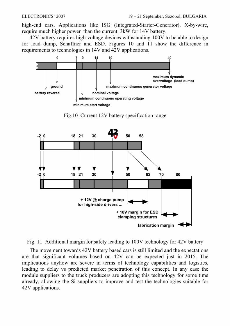
42V battery requires high voltage devices withstanding 100V to be able to design for load dump, Schaffner and ESD. Figures 10 and 11 show the difference in requirements to technologies in 14V and 42V applications.
0
maximum dynamic overvoltage (load dump)
maximum continuous generator voltage
nominal voltageminimum continuous operating voltage
minimum start voltage
ground
battery reversal
7 9 19 4014
Fig.10 Current 12V battery specification range
0-2
+ 12V @ charge pumpfor high-side drivers ...
18 21 30 50 62
0-2 18 21 30 50 58
70 80
+ 10V margin for ESDclamping structures
fabrication margin
Fig. 11 Additional margin for safety leading to 100V technology for 42V battery The movement towards 42V battery based cars is still limited and the expectations
are that significant volumes based on 42V can be expected just in 2015. The implications anyhow are severe in terms of technology capabilities and logistics, leading to delay vs predicted market penetration of this concept. In any case the module suppliers to the truck producers are adopting this technology for some time already, allowing the Si suppliers to improve and test the technologies suitable for 42V applications.
ELECTRONICS’ 2007 19 – 21 September, Sozopol, BULGARIA
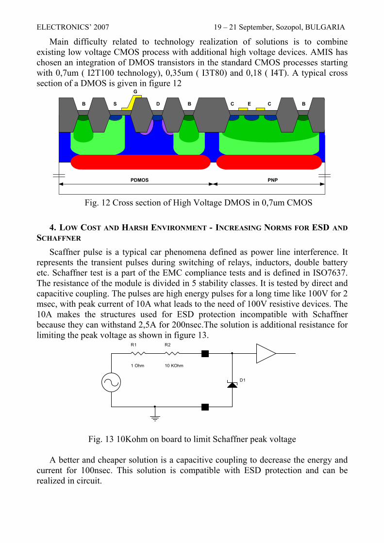
Main difficulty related to technology realization of solutions is to combine existing low voltage CMOS process with additional high voltage devices. AMIS has chosen an integration of DMOS transistors in the standard CMOS processes starting with 0,7um ( I2T100 technology), 0,35um ( I3T80) and 0,18 ( I4T). A typical cross section of a DMOS is given in figure 12
PDMOS PNP
B S
G
D B BC CE
Fig. 12 Cross section of High Voltage DMOS in 0,7um CMOS
4. LOW COST AND HARSH ENVIRONMENT - INCREASING NORMS FOR ESD AND
SCHAFFNER Scaffner pulse is a typical car phenomena defined as power line interference. It
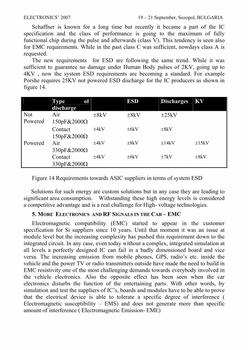
represents the transient pulses during switching of relays, inductors, double battery etc. Schaffner test is a part of the EMC compliance tests and is defined in ISO7637. The resistance of the module is divided in 5 stability classes. It is tested by direct and capacitive coupling. The pulses are high energy pulses for a long time like 100V for 2 msec, with peak current of 10A what leads to the need of 100V resistive devices. The 10A makes the structures used for ESD protection incompatible with Schaffner because they can withstand 2,5A for 200nsec.The solution is additional resistance for limiting the peak voltage as shown in figure 13.
D1
R1
1 Ohm
R2
10 KOhm
Fig. 13 10Kohm on board to limit Schaffner peak voltage A better and cheaper solution is a capacitive coupling to decrease the energy and
current for 100nsec. This solution is compatible with ESD protection and can be realized in circuit.
ELECTRONICS’ 2007 19 – 21 September, Sozopol, BULGARIA
Schaffner is known for a long time but recently it became a part of the IC specification and the class of performance is going to the maximum of fully functional chip during the pulse and afterwards (class V). This tendency is seen also for EMC requirements. While in the past class C was sufficient, nowdays class A is requested.
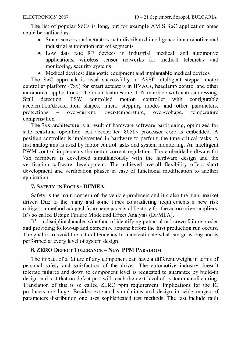
The new requirements for ESD are following the same trend. While it was sufficient to guarantee no damage under Human Body pulses of 2KV, going up to 4KV , now the system ESD requirements are becoming a standard. For example Porshe requires 25KV not powered ESD discharge for the IC producers as shown in figure 14.
Type of
discharge ESD Discharges KV
Not Powered
Air 150pF&2000Ω
±8kV ±8kV ±25kV
Contact 150pF&2000Ω
±4kV ±6kV ±8kV
Powered Air 330pF&2000Ω
±4kV ±8kV ±14kV ±15kV
Contact 330pF&2000Ω
±4kV ±6kV ±7kV ±8kV
Figure 14 Requirements towards ASIC suppliers in terms of system ESD Solutions for such energy are custom solutions but in any case they are leading to
significant area consumption. Withstanding these high energy levels is considered a competitive advantage and is a real challenge for High- voltage technologies.
5. MORE ELECTRONICS AND RF SIGNALS IN THE CAR – EMC Electromagnetic compatibility (EMC) started to appear in the customer
specification for Si suppliers since 10 years. Until that moment it was an issue at module level but the increasing complexity has pushed this requirement down to the integrated circuit. In any case, even today without a complex, integrated simulation at all levels a perfectly designed IC can fail in a badly dimensioned board and vice versa. The increasing emission from mobile phones, GPS, radio’s etc. inside the vehicle and the power TV or radio transmitters outside have made the need to build in EMC resistivity one of the most challenging demands towards everybody involved in the vehicle electronics. Also the opposite effect has been seen when the car electronics disturbs the function of the entertaining parts. With other words, by simulation and test the suppliers of IC’s, boards and modules have to be able to prove that the electrical device is able to tolerate a specific degree of interference ( Electromagnetic susceptibility – EMS) and does not generate more than specific amount of interference ( Electromagnetic Emission- EME)
ELECTRONICS’ 2007 19 – 21 September, Sozopol, BULGARIA
To reduce the risk at final assembly of the vehicle, each level of hierarchy is subjected to different types and levels of testing depending on the connectivity. We distinguish three main levels, modules, PCB and Integrated Circuit(IC). IC’s and boards because of their dimensions are not tested in absorbed line chambers but by applying high frequency current or power directly on the pins.
Radiated emission and susceptibility is not the major problem for IC’s. Conducted emission and susceptibility to the efficient antennas on the PCB and
the cable harness is the difficult to solve problem. Two EMS conductive methods, compatible with simulation, have been
standardized in IEC 62132-4 (DPI – Direct Power Injection) [1]. ISO 7637 (Schaffner) [3], [4], [5] is compatible to the last. The EME tests are defined as RF emission with direct coupling in IEC61967- 4 [2] and conducted emission in CISPR 25, chapter 6.2.2.2 [6].
These methods model conducted EMC between IC and PCB, not the Electromagnetic (EM) -field. Generated EM-fields are function of module and wiring layouts. Limit setting for these methods is based on the accumulated experience of the chip and module manufacturers.
A company can have a competitive advantage if the design team is in position to design for EMS and EME. Still the biggest challenges are related to integrated design approach applicable to constantly increasing complexity and requirements. The main issue in simulating the EMC is the right representation of the involved components and their ideality under RF emission. In any case the PCB components play an important role and the involvement of the PCB makers is very important if one wants to create a realistic modeling environment.
6. SMALLER AND CHEAPER – SYSTEM ON A CHIP APPROACH The complex functional requirements determine the System on a Chip (SoC) as a
wide-ranging design approach. Mixed signal technology is the base of the SoC, providing real world continuous analog signal interface to a complex digital part. Depending on the speed and computational requirements, an appropriate processor architecture must be used. The main components of the architecture are: instruction set, data processing unit(s), data path width and instruction width. If IP reuse is possible, a suitable processor core must be selected. Single core system is common now, but SoCs with two different cores are also frequently used. Power management and low power design are mandatory for automotive SoC solutions. Peripherals are important component of SoC design approach. They depends on particular interface requirements:
• DAC, ADC and signal conditioning units • UARTs for LIN, RS232, SPI and other simple serial interfaces • CAN, Zigbee, FlexRay … • LAN MAC
Specific requirements are applied to the peripherals and the process technology of automotive SoCs.
ELECTRONICS’ 2007 19 – 21 September, Sozopol, BULGARIA
The list of popular SoCs is long, but for example AMIS SoC application areas could be outlined as:
• Smart sensors and actuators with distributed intelligence in automotive and industrial automation market segments
• Low data rate RF devices in industrial, medical, and automotive applications, wireless sensor networks for medical telemetry and monitoring, security systems
• Medical devices: diagnostic equipment and implantable medical devices The SoC approach is used successfully in ASSP intelligent stepper motor
controller platform (7xx) for smart actuators in HVACs, headlamp control and other automotive applications. The main features are: LIN interface with auto-addressing; Stall detection; ESW controlled motion controller with configurable acceleration/deceleration shapes, micro stepping modes and other parameters; protections – over-current, over-temperature, over-voltage, temperature compensation.
The 7xx architecture is a result of hardware-software partitioning, optimized for safe real-time operation. An accelerated 80515 processor core is embedded. A position controller is implemented in hardware to perform the time-critical tasks. A fast analog unit is used by motor control tasks and system monitoring. An intelligent PWM control implements the motor current regulation. The embedded software for 7xx members is developed simultaneously with the hardware design and the verification software development. The achieved overall flexibility offers short development and verification phases in case of functional modification to another application.
7. SAFETY IN FOCUS - DFMEA Safety is the main concern of the vehicle producers and it’s also the main market
driver. Due to the many and some times contradicting requirements a new risk mitigation method adopted from aerospace is obligatory for the automotive suppliers. It’s so called Design Failure Mode and Effect Analysis (DFMEA).
It’s a disciplined analysis/method of identifying potential or known failure modes and providing follow-up and corrective actions before the first production run occurs. The goal is to avoid the natural tendency to underestimate what can go wrong and is performed at every level of system design.
8. ZERO DEFECT TOLERANCE – NEW PPM PARADIGM The impact of a failure of any component can have a different weight in terms of
personal safety and satisfaction of the driver. The automotive industry doesn’t tolerate failures and down to component level is requested to guarantee by build-in design and test that no defect part will reach the next level of system manufacturing. Translation of this is so called ZERO ppm requirement. Implications for the IC producers are huge. Besides extended simulations and design in wide ranges of parameters distribution one uses sophisticated test methods. The last include fault
ELECTRONICS’ 2007 19 – 21 September, Sozopol, BULGARIA
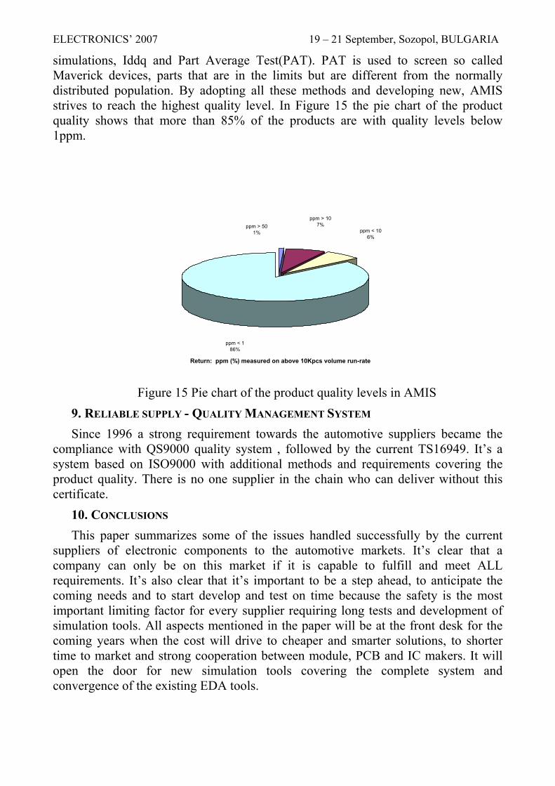
simulations, Iddq and Part Average Test(PAT). PAT is used to screen so called Maverick devices, parts that are in the limits but are different from the normally distributed population. By adopting all these methods and developing new, AMIS strives to reach the highest quality level. In Figure 15 the pie chart of the product quality shows that more than 85% of the products are with quality levels below 1ppm.
Return: ppm (%) measured on above 10Kpcs volume run-rate
ppm > 501%
ppm > 107%
ppm < 106%
ppm < 1 86%
Figure 15 Pie chart of the product quality levels in AMIS
9. RELIABLE SUPPLY - QUALITY MANAGEMENT SYSTEM Since 1996 a strong requirement towards the automotive suppliers became the
compliance with QS9000 quality system , followed by the current TS16949. It’s a system based on ISO9000 with additional methods and requirements covering the product quality. There is no one supplier in the chain who can deliver without this certificate.
10. CONCLUSIONS This paper summarizes some of the issues handled successfully by the current
suppliers of electronic components to the automotive markets. It’s clear that a company can only be on this market if it is capable to fulfill and meet ALL requirements. It’s also clear that it’s important to be a step ahead, to anticipate the coming needs and to start develop and test on time because the safety is the most important limiting factor for every supplier requiring long tests and development of simulation tools. All aspects mentioned in the paper will be at the front desk for the coming years when the cost will drive to cheaper and smarter solutions, to shorter time to market and strong cooperation between module, PCB and IC makers. It will open the door for new simulation tools covering the complete system and convergence of the existing EDA tools.
ELECTRONICS’ 2007 19 – 21 September, Sozopol, BULGARIA
What are the next coming challenges? If we follow the development of the cars, we’ll see that related to the engine and the driver we move to taking an outside objective control over both. While in the beginning the driver had to be technically skilled and was not expected to have high driving skills, now it’s opposite, the driving skills are very important and no need of technical skills is required. The tendency is to get to more and more control over the driving skills and to avoid risk on the roads. A step already taken is the optical surveillance of the driver and increasing amount of signals improving his attention. The next step is the elimination of the subjective role of the driver. It will be the role of telematics allowing the cars to communicate with each other, the roadside infrastructure and the traffic control centers. Integrated sensors in a global network, camera’s , reliable WLAN and embedded software are what the industry needs.
Other point of interest due to the environmental and cost aspects is the power train with hybrid solutions using electrical batteries or fuel cells to improve emission and decrease the dependence on oil.
The Vehicle technology game is a never ending story and being part of it is difficult but very exiting.
Thanks to all colleagues of AMIS providing me with materials for this paper. Special thanks to Aarnaut Wieers, Herman Casier, Geert Vandesande, Daniel Vandestraeten for the data provided. The data is published on internal AMIS Engineering Forum and reports.
11. REFERENCES [1] IEC 62132-4, Integrated circuits - Measurement of electromagnetic immunity 150 kHz to 1
GHz - Part 4: Direct RF power injection method, 2006-02 [2] IEC/TS 61967-4, Integrated circuits - Measurement of electromagnetic emissions, 150 kHz
to 1 GHz - Part 4: Measurement of conducted emissions - 1 Ω/150 Ω direct coupling method, 2006-07
[3] ISO 7637-1:2002, Road vehicles -- Electrical disturbances from conduction and coupling -- Part 1: Definitions and general considerations
[4] ISO 7637-2:2004, Road vehicles -- Electrical disturbances from conduction and coupling -- Part 2: Electrical transient conduction along supply lines only
[5] ISO 7637-3:2007, Road vehicles -- Electrical disturbances from conduction and coupling -- Part 3: Electrical transient transmission by capacitive and inductive coupling via lines other than supply lines
[6] CISPR 25, Radio disturbance characteristics for the protection of receivers used on board vehicles, boats, and on devices - Limits and methods of measurement, 2002-08