Embed Size (px)
Citation preview

Abstract—While looking for new opportunities to transfer
data in the industrial field level, we already achieved various partial successes. In previous conducted studies, it was possible to demonstrate viable options to transmit a large amount of data faster over a simple unshielded line. The system power can also be provided via the same communication medium. We developed a possibility to transfer data using a special adapted multi-carrier modulation scheme. Our communication method can be used for point-to-point, multipoint or even multipoint-to-multipoint connections. Now all this prototypical processes should be brought to an ASIC Design. But we indicated different problems when trying to integrate the designed low voltage digital part and also a bus powered voltage converter (30V to 3.3V) for the internal ASIC supply. Both could not be integrated cost-effective enough on the same die. So a separate external power supply is needed. The increasing number of up to 128 power supply units connected to the same bus line, are leading to a lot of communication problems. In this paper we show some occurred problems, measured with our experimental setup. We show different possible variants of energy extraction and discuss some practical solutions.
Index Terms — industrial communication, multi carrier allocation, unshielded wire, external ASIC power supply unit
I. INTRODUCTION
n recent years, always growing industrial plants and a constantly rising level of automation increase the system
complexity. Also the need for more and more system participants was growing enormously. Now the industrial Ethernet has nearly completely arrived all factory levels and is almost grown to the actual standard. However, there are still systems and areas in which the use of industrial Ethernet is not worthwhile or simply undesired. Analyzing currently used industrial communication standards, it quickly becomes aware, that the transfer of user data and system power over a single communication medium is hardly used. This results from the history of communication systems development, but also on the large number of problems when trying to modulate user data on an energy supply in harsh industrial environments [1][2]. It was already successfully demonstrated, that technics of fast data communication and multimedia technologies could also be used for process and factory automation systems.
Manuscript received July 19, 2016; revised August 8, 2016.
All Authors are employees of the HTWK Leipzig, Wächterstr. 13, 04107 Leipzig, Germany, ([email protected], [email protected], [email protected], www.ftz-leipzig.de) or former student of the HTWK Leipzig (Patrik Uschmann)
The much higher requirements on data and noise immunity in industrial environments can be completely achieved. We realized and tested a modified OFDM modulation in which the used carriers are organized in a Time Division Multiple Access (TDMA) scheme. The basic concept of the multi-channel transmission is to split a data signal with high bitrates into a plurality of data signals with lower bitrates to transmit them simultaneously parallel on different sub-channels in the following called carriers.
Fig. 1. Structure of a communication cycle (one transmitter / x receivers)
Each participant (from here now called client) is allocated one or more carriers and this frequency composition is subsequently modulated to the 30V supply voltage (Fig. 1). The system topology allows line, tree, star and ring structures with a total cable length of more than 100 meters. So from theory the OFDM scheme is best suitable for the parallel transmission of a large number of bits. The additional multiplex method should be used to achieve an optimum utilization of the line and frequency range. [3][4][5]
After examining the 30V bus line power supplies influence for the used transmission method, the possibilities of energy extraction through up to 128 connected clients should now be analyzed. This paper should disclose possible options to provide enough energy for a large number of connected ASICs without disturbing the bus line communication.
II. BASIC CONSIDERATION FOR ENERGY
EXTRACTION
In all previous experimental setups, the used clients were not directly powered out of the bus lines 30V. They all were powered from an external laboratory power supply. A supply from up to 128 possible clients out of the same bus line could lead to heavy physical difficulties. Previous problems with examined standard power supplies for the needed 30V bus line supply voltage already indicated
Analyzing Variants of Multiple Energy Extraction from a Prototypic Multi-flexible Bus
System for Industrial Environment
Tobias Rudloff*, Dietmar Telschow*, Patrik Uschmann*, Tilo Heimbold*
I
Proceedings of the World Congress on Engineering and Computer Science 2016 Vol I WCECS 2016, October 19-21, 2016, San Francisco, USA
ISBN: 978-988-14047-1-8 ISSN: 2078-0958 (Print); ISSN: 2078-0966 (Online)
WCECS 2016
potentially occurring problems when designing the ASICs power unit modules. One problem here represents the switching frequency when using power supplies based on switching regulators. If this frequency is in the range of the used data transmission frequency band, this leads to a considerable noise level and a degradation of the user data SNR. These problems, regarding to symmetry adaption and impedance influences through the bus line connected single 30V power supply unit, are manageable. With up to 128 bus clients and therefore 128 5V/3.3V power units, a special know-how and also an intuition for fine-tuning is urgently needed.
Fig. 2. Differential signal transmission over the bus line and needed
separate power extraction for the clients
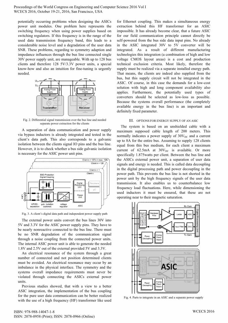
A separation of data communication and power supply via bypass inductors is already integrated and tested in the client’s data path. This also corresponds to a galvanic isolation between the clients signal IO pins and the bus line. However, it is to check whether a bus side galvanic isolation is necessary for the ASIC power unit pins.
Fig. 3. A client’s digital data path and independent power supply path
The external power units convert the bus lines 30V into 5V and 3.3V for the ASIC power supply pins. They have to be nearly nonreactive connected to the bus line. There must be no SNR degradation of the communication signal through a noise coupling from the connected power units. The internal ASIC power unit is able to generate the needed 1.8V and 2.5V out of the external provided 5V and 3.3V.
An electrical resonance of the system through a great number of connected and not position determined clients must be avoided. An electrical resonance may occur by an imbalance in the physical interface. The symmetry and the systems overall impedance requirements must never be violated through connecting the ASICs external power units.
Previous studies showed, that with a view to a better ASIC integration, the implementation of the bus coupling for the pure user data communication can be better realized with the use of a high frequency (HF) transformer like used
for Ethernet coupling. This makes a simultaneous energy extraction behind this HF transformer for an ASIC impossible. It has already become clear, that a future ASIC for our field communication principle cannot directly be self-powered from the bus side data input pins. No already in the ASIC integrated 30V to 5V converter will be integrated. As a result of different manufacturing technologies this integration (a combination of high and low voltage CMOS layout areas) is a cost and production technical exclusion criteria. Most likely, therefore the supply must be realized via a separate installed energy path. That means, the clients are indeed also supplied from the bus, but this supply circuit will not be integrated in the ASIC. Of course, in this case the demands for a low-cost solution with high and long component availability also applies. Furthermore, the potentially used types of converters should be selected as low-loss as possible. Because the systems overall performance (the completely available energy in the bus line) is an important and definitely fixed parameter.
III. OPTIONS FOR ENERGY SUPPLY OF AN ASIC
The system is based on an unshielded cable with a maximum supposed cable length of 200 meters. This normally indicates a power supply of 30VDC and a current up to 8A for the entire bus. Assuming to supply 128 clients equal from this bus medium, for each client a maximum current of 62.5mA at 30VDC is available. Or more specifically 1.875watts per client. Between the bus line and the ASICs external power unit, a separation of user data signals and energy is needed. This is called data decoupling in the digital processing path and power decoupling in the power path. This prevents the bus line is not shorted in the power unit by the high frequency signals of the user data transmission. It also enables us to counterbalance low frequency load fluctuations. Here, while dimensioning the used inductors it must be ensured, that these are not operating near to their magnetic saturation.
Fig. 4. Parts to integrate in an ASIC and a separate power supply
Proceedings of the World Congress on Engineering and Computer Science 2016 Vol I WCECS 2016, October 19-21, 2016, San Francisco, USA
ISBN: 978-988-14047-1-8 ISSN: 2078-0958 (Print); ISSN: 2078-0966 (Online)
WCECS 2016

It is assumed that each client ASIC requires external 5V and 3.3V supply voltage and has a power requirement of about 1 watt. In view of an interference-free transmission, the required power unit’s bus side inputs should produce a particular noise level of less than 20mVpp. This bus side circuit inputs should never disturb the symmetry of the bus line. The need for a galvanic isolation must be examined by evaluating the error rate of user data frames under external EMC stimulation. This is called a burst measurement. If predetermined maximum error rates cannot be supported for certain specified power unit circuits, this leads to the exclusion of that power converter type.
Regarding to the later use of the clients as sensors or actuators in smallest industrial design housings, it will be necessary to ensure the temperature development of the overall design (ASIC + power unit) won’t be unnecessarily high. A high as possible efficiency should be considered more in detail here. The availability of components over a longer period should also not be neglected. In order to meet the compliance of a symmetrical bus coupling, some simple solder pads for resistor and capacitor can be integrated to the power unit connection printed circuit board (PCB). A readjustment is then effected by equipping the respective missing capacitive and/or resistive symmetry components. In the following we will discuss variants of power supply options, which are possible for up to 128 of these external ASIC power units.
In the upper part Figure 4 shows the design of one discrete realized client. In the lower part it shows the possibility of an ASIC integration combined with an external power unit to provide the ASICs 5V and 3.3V power supply.
IV. ADVANTAGES AND DISADVANTAGES OF
DIFFERENT SOLUTIONS
Linear Regulator: At first, variants with linear regulators should be reviewed. For example here is a possibility to establish a series connection of different linear regulators. Because linear regulators work like a variable resistor, they have the advantage of producing no noise caused by any switching circuit component. Therefore, they are almost reactionless contactable and usually of a compact size.
Fig 5. Series connection of different linear regulators
The variant a) of figure 5 represents in this case the simplest possible variant for a 30V to 5V to 3.3V power path. The high voltage difference between input and output voltage is resulting in a very low efficiency of the circuit. This will be displayed in a high power consumption and a very high thermal loss dependent on the output current. Here a heatsink to the 5V regulator should definitely be
attached. With regard to the desired very small size of future produced sensor and actuator clients, that is no practicable solution.
The variant b) in the figure 5 would be the possibility to reduce the thermal dissipation with placing a 15V regulator in front of the 5V regulator. Nevertheless, this variant includes an additional problem. Considering the required currents, it is quite clear that the 5V regulator will not only provide the current for the 5V path of the ASIC, it additional also has to provide the current for the 3.3V path. This is not particularly efficient, because the 5V regulator must be significantly higher dimensioned here and will also emit unnecessary electrical power in form of heat.
Fig. 6. Ripped power paths a) directly connected to the bus line b) on the outputs of an interconnected 15V linear regulator
A better option would be the structure shown in figure 6 a. In theory, this variant a) can be realized very simple and space saving. But the voltage drop across the 3.3V and the 5V regulators is even greater in this case and the thermal power dissipation in both paths (3.3V and 5V regulator) will be very high. The 3.3V and the 5V paths are separated, so that each regulator only supply the needed current at his voltage path. Hence the regulators can be dimensioned smaller and the power loss can be minimized again, but the difference between 30VDC and 3.3V is enormously. In each case the variant shown in figure 6 b should be preferred and perhaps the 15V to 3.3V path is to split into even more drops.
DC/DC-Converter: Now we consider some variants with DC/DC converters. In that case the voltage conversion is realized via a periodically operating electronic switch with an attached energy storage. Again, there is the possibility of a series connection of various DC/DC converters.
Since DC/DC converters have a much higher efficiency than linear regulators, a previous mounted 15V converter can be omitted. Furthermore, a DC/DC converter would simultaneously act as a galvanic isolation and in some cases also as an input filter for the physical bus line. Another disadvantage, not to be underestimated, is the usually high price compared to linear regulators and the often larger PCB footprint. A heatsink can be omitted because of the DC/DC converters operating mode. Also negative classified are the occurring switching frequencies resulting from the used electronic switch principle of this converter types. As mentioned above, under certain circumstances this could have some negative effects to the user data communication. An enormous technical effort has been made from the
Proceedings of the World Congress on Engineering and Computer Science 2016 Vol I WCECS 2016, October 19-21, 2016, San Francisco, USA
ISBN: 978-988-14047-1-8 ISSN: 2078-0958 (Print); ISSN: 2078-0966 (Online)
WCECS 2016

manufacturers, to free the output voltage from these disturbing switching frequencies. In most cases, they are untouched on the converters input side and disturbing frequency spikes are clearly to identify. For the present prototyping case, these converters are not really reactionless coupled to the bus line side.
Fig. 7. Variants of connecting DC/DC converters to the bus line
When using DC/DC converters in the described application, using separate voltage levels (see figure 7 a) is more preferable than a series connection. This allows a smaller dimensioning of the finally selected 5V converter. Unfortunately, an amplified noise level will be a disadvantage of this circuit variant. Without additional filtering the inputs of the interconnected converters, their switching noise is added and amplified on the bus line side. A custom input filter is unavoidable at this point. However, the behavior to the bus line side should be examined in the following paper section using an example of 2 specific DC/DC regulator types.
Combined circuit: In figure 8, the possibilities of a mixed assembly of using linear regulators and DC/DC converters is shown schematically. When selecting a combined circuit setup, a variant with upstream connected DC/DC converter followed by a linear regulator should be chosen. Due to the improved efficiency and the galvanic isolation through the DC/DC converter, this variant represents the optimum. For input noise suppression the DC/DC converter should be ideally equipped with an input filter. Otherwise, in that case an additional filter must also be designed. This combined circuit variant provides a low power dissipation and electrical isolation. But it might have higher space requirements and also higher costs than a pure linear regulator variant.
Fig. 8. Mixed assembly of DC/DC converter and linear regulator types
Discrete structure: Finally, even briefly the possibility of a discrete ASIC voltage supply should be mentioned. Because there are countless variants and they all could be indirectly derived from the variants shown before (linear regulator, DC/DC converter with charge pump, buck or boost converters, it should not be discussed more in detail here.
V. RESULTS AND COMPARISONS OF DIFFERENT
VARIANTS
In this chapter we describe and compare our results of an experimental setup of different regulator types. We measured all the devices behavior connected with their input to our prototypical multi-flexible bus system. So we get real impressions of the negative influences to our communication method.
Linear regulator: Our study examined the ON Semiconductor linear regulator types MC7815 and MC33269 to their absence of reaction, their current and voltage ratios, impedance behavior and symmetry properties.
Between the tested linear regulators and the bus line a power decoupling unit for the separation of user communication data and power supply was implemented. The power decoupling consist of two inductors and two parallel wired resistors. A really basic schematic of a possible power decoupling is shown in figure 9. The resistors placed serial to the capacitors are for adjusting the symmetry behavior of the circuit coupling to the bus line.
Fig. 9. Power decoupling for separate user data from the power supply
The measurements in figure 10 shows that with increasing load the output voltage is decreasing. At an output current of 250mA, the deviation of the required 5V output voltage is already 0.3V or 6 percent. When using the maximum cable length of about 200m, the voltage drop across the line is already about 6 to 7V. So there is maybe not enough energy in the overall system to provide stable 5V and 3.3V supply voltages for every client. That is a big system disadvantage.
Fig. 10 Input to output current behavior of a linear regulator
Looking at the data series for inductance and capacitance, a significant drop between 75mA and 100mA output current is visible. This results from the saturation area of the inductors used in the power decoupling circuit. Unfortunately, the selected inductors run to saturation at a
Proceedings of the World Congress on Engineering and Computer Science 2016 Vol I WCECS 2016, October 19-21, 2016, San Francisco, USA
ISBN: 978-988-14047-1-8 ISSN: 2078-0958 (Print); ISSN: 2078-0966 (Online)
WCECS 2016

current of about 90mA. So the inductive part slopes rapidly and the resistance part of the coil is becoming more important and finally dominant. So the biggest part of the electrical power is converted into heat. So this inductor is more behaving like a simple resistor. The thermal dissipation increases rapidly.
The used inductors were selected based on the lowest parasitic capacity to stress the bus line as less as possible. The used inductors do not met the current carrying capacity for the later required external energy supply of the ASIC. But for the first test scenarios they were perfectly adequate. After the output current of the linear regulator has reached about 75mA, unfortunately the used inductors have reached their saturation. This leads to a drop of the capacitance and inductance and also to an asymmetry of the circuit bus line coupling. For output currents over 75mA no meaningful symmetry measurement could be done. There was no measurable capacitance and inductance anymore for this circuit. The user data communication quality will fail because of that strong bus line asymmetry.
Fig. 11. Inductivity and capacity behavior with increasing output current
Fig. 12. Symmetry behavior with increasing output current
DC/DC converter: In our study we examined also the DC/DC converter types RECOM RP08-2405SAW (from here only called Recom) and TRACO POWER TES3-2411 (from here only called Traco) to their absence of reaction, their current and voltage ratios, impedance behavior and symmetry properties.
Fig. 13. Example of a schematic power decoupling
RECOM: Measurements at the bus line side input of the converter demonstrated a noise level of about 580mVpp resulting from two frequency components at about 117MHz. They are significantly higher than the frequency band used for the user data communication on the bus line. The study of this data frequency band only shows a few narrow-band spikes at 50mA electrical load. These visible spikes are about -65dBm and not really dangerous for the data communication using our OFDM scheme. Also, no significant changes could be determined for different load magnification (figure 14).
Fig. 14. Frequency spectrum Recom converter with 50mA load
TRACO: Looking at the Traco converter it has a visible higher noise level, even without any load. But this is a factor 10 smaller than the sporadic spikes of the Recom converter. The working range of the Traco converter is in the range of 230kHz to 32MHz. Unfortunately the occurring noise frequencies are exactly falling into the used communication band. This will heavy influence the data communication. So maybe the number of available carriers will decrease. In the recorded spectrum (figure 15) the most significant noise peaks can be seen. The maximum amplitude is at -42.3dBm and at a frequency of 3.3229MHz. Here we have a very high probability of communication failure.
Fig. 15. Frequency spectrum Traco converter with 50mA load
With increasing load, the frequency of the noise spikes reduces visible. In the used prototypical bus system this would result in an improvement or degradation of certain carriers when varying the load conditions. Then this leads to a permanent carrier change of the active clients and a raising failure rate. Compared to the tested linear regulators, a much lower input current should be needed when using the DC/DC converter variant. This should lead to higher output currents without the problem of the used data decoupling coils going into the saturation.
The behavior of capacitance and inductance are nearly
Proceedings of the World Congress on Engineering and Computer Science 2016 Vol I WCECS 2016, October 19-21, 2016, San Francisco, USA
ISBN: 978-988-14047-1-8 ISSN: 2078-0958 (Print); ISSN: 2078-0966 (Online)
WCECS 2016

constant up to an output current of 270 mA. Taking out more current of the converter circuit, the inductance of both DC/DC converters will fall. The capacitance of the Traco converter will nearly stay constant while the capacitance of the Recom converter will also fall (see figure 17). For an output current up to 250 mA, the results of the symmetry measurement (see figure 18) are very good and clearly superior to the circuits built up with linear regulators.
Our measurements show clearly the advantages of using a DC/DC converter. If the much higher occurring noise and the occurring spikes are not inside or in the near of the used data communication frequency spectrum.
Fig. 16. Input to output current behavior of a DC/DC converter
Fig. 17. Inductivity and capacity behavior with increasing output current
Fig. 18. Symmetry behavior with increasing output current
In a subsequent burst measurement (burst pulses up to 1kV), no significant differences between linear regulators and DC/DC converters in reference on the stability of user
data communication could be detected. So, for a prototypical design with up to 128 clients, using the DC/DC converters from Recom followed by a linear regulator to provide the 5V and 3.3V would be quite suitable.
VI. CONCLUSION
Each of the variants shown and tested, is representing a compromise. There will be no hundred percent optimal structure of an external ASIC power unit for our case. However, factors such as the effects back to the bus line and the compliance of symmetry are to prioritize all the other parameters. The DC/DC converters narrow-band noise is very pronounced in the level. But this definitely depends on the used type and so it is user selectable in a way that the communication frequencies are outside this noise range. Not acceptable are potentially load dependencies of these interferences in certain types of converters. Because a relevant advantage of the prototyped bus system is its free and flexible topology selection, it provides under certain circumstances a criteria for exclusion of certain converter types.
For a use in real products (sensors, actuators or I/O modules), no out of the box ready DC/DC converter types could be used because of their potentially very large design size and their high costs compared to the most linear regulator circuits. Maybe some new DC/DC converters from ALTERA, special offered for the use in combination with FPGAs, are a suitable alternative for the needed external ASIC power units. These converters are very small (only a 3x4 mm package) and work as synchronous buck converters. But this must still be verified and tested under real conditions.
The comparisons and evaluations of the measurements have shown, that a galvanic isolation is not absolutely necessary for the tested prototyping designs. If in a future designed ASIC solution for industrial use, a galvanic isolation should not be necessary, a solutions with simple linear regulators would also be conceivable. However, here the thermal losses and the strain of the bus lines 30V power capacities should be examined carefully.
REFERENCES [1] G. Schnell, “Bussysteme in der Automatisierungstechnik –
Grundlagen und Systeme der industriellen Kommunikation” Braunschweig/Wiesbaden: Vieweg Verlag, 2000.
[2] VDI Standard 3687, “Selection of field bus systems by evaluating their performance characteristics for industrial applications” Berlin: Beuth-Verlag, 1999.
[3] J. A. C. Bingham, “Multicarrier modulation for data transmission: an idea whose time has come.” IEEE Communications Magazine, Vol. 28, Nr.5, pp. 5 -14, May 1990.
[4] I. Kalet, “The multitone channel” IEEE Communications Magazine, Vol. 37, Nr.2, pp. 119-124, February 1989.
[5] J. W. Cook, R. H. Kirkby, M. G. Booth, K. T. Foster, D. E. A. Clarke, G. Young, “The noise and crosstalk environment for ADSL and VDSL systems” IEEE Communications Magazine, Vol. 37, Nr.5, pp. 73-78, May 1999.
[6] M. H. Hayes, “Statistical Digital Signal Processing and Modeling” John Wiley & Sons, 1996.
[7] R. Schur, “Impulse compression for OFDM transmission over time-varying multipath channels” IEEE Vehicular Technology Conference (VTC), September 2002.
[8] B. R. Saltzberg “Comparison of Single-carrier and multitone digital modulation for ADSL applications” IEEE Communications Magazine, Vol. 36, Nr.11, pp. 114-121, November 1998.
Proceedings of the World Congress on Engineering and Computer Science 2016 Vol I WCECS 2016, October 19-21, 2016, San Francisco, USA
ISBN: 978-988-14047-1-8 ISSN: 2078-0958 (Print); ISSN: 2078-0966 (Online)
WCECS 2016

[9] D. M. Welton, “Transmission Lines: Theory, Types and Applications” (Electrical Engineering Developments) [Hardcover], Nova Science Pub Inc, pp. 221-236, November 2011.
[10] T. Handte, M. Breuninger, H. T. Hagmeyer, J. Speidel, ”Physical layer of a novel broadband low-level fieldbus with discrete multitone“ In Factory Communication Systems (WFCS), 2012 9th IEEE International Workshop on, S. 173–176, May 2012.
[11] T. Rudloff, A. Fink, M. Voß, M. Flügge, K. P. Kirchner, T. Heimbold, H. Beikirch, ”Emulation of a digital Process-Oriented Real-Time Communication Circuit”. PDES 2012 Brno, S.286-290
[12] T. Rudloff, D. Telschow, M. Flügge, T. Heimbold, “Multicarrier-Modulation for Process-Oriented Real-Time Communication Techniques in Industrial Enviroment”. Tagungsband WCECS 2012 San Francisco, S. 854-859. ISBN: 978-988-19252-4-4, ISSN: 2078-0958.
Proceedings of the World Congress on Engineering and Computer Science 2016 Vol I WCECS 2016, October 19-21, 2016, San Francisco, USA
ISBN: 978-988-14047-1-8 ISSN: 2078-0958 (Print); ISSN: 2078-0966 (Online)
WCECS 2016