Embed Size (px)
Citation preview
Progress In Electromagnetics Research B, Vol. 63, 187–201, 2015
Analysis of the Proximity Coupling of a Planar Array Quasi-LumpedElement Resonator Antenna Based on Four Excitation Sources
Seyi S. Olokede1, * and Clement A. Adamariko2
Abstract—In this paper, a simple-fed, low profile, 9× 10 elements quasi-lumped planar antenna arrayis presented. The proposed resonator employs a quasi-lumped element resonator that uses interdigitalcapacitor (IDC) in parallel with a straight strip inductor shorted across the capacitor. The arrayelements were designed and then excited by a feed network of four coaxial probes situated at thebottom plane but separated from the ground plane using a plastic material. The entire array is dividedinto four sub-array lattices of 5× 5 elements and excited by a coaxial probe located at the centre of thesub-arrays antenna structure, thus exciting the centre resonator who in turn excites the neighbouringelements via proximity coupling. The probes are connected based on Wilkinson power divider principleto provide in-phase excitation. An explicit method is introduced to quickly obtain the array factor (AF)characteristics for such proximity coupled rectangular planar array. Radiation pattern and the arrayfactor are presented, and are further compared with those obtained by the simulation and experimentalresults. The proposed antenna comprises 9 × 10 elements array, each of which is 5.8 × 5.6 sq. mm insize, and the entire antenna structure is about 120 × 80 sq. mm.
1. INTRODUCTION
Usually, lumped element resonators are formed by lumped inductors and capacitors. These lumpedelement resonators are passive components whose sizes across any dimension are much smaller than theoperating wavelength to ensure that there is no appreciable phase shift between the input and outputterminals. Their no-phase shift tendency underscores their usefulness. As a result, most literaturesrecommend that the length of an equivalent inductor and capacitor elements should not be longerthan λ/20 or 12% of its wavelength of operation. Otherwise, it will lose its lumped equivalencyeffect. However, Janhsen et al. [1] asserted that a general definition of quasi lumped elements cannotbe established particularly with reference to its length, because it would be somewhat arbitrary.Incidentally (according to them), the width w of an impedance sections has only a small effect onthe scattering parameters in comparison with the length l, where the height h of the sections is orientedtransversely to the current flow. Of particular interest therefore is the definition of Hong where he definedquasi-lumped element as microstrip line short sections and stubs whose physical lengths are smallerthan a quarter of guided wavelength at which they operate, and as such, are common components forapproximate microwave realization of lumped elements in microstrip filters structures, and are termedquasi-lumped elements [2]. It is on the basis of this definition that the proposed derives its lumpedelement equivalency. They therefore have the relative advantage of smaller size, wider bandwidth, andmore particularly, lower cost characteristics. Thus, impedance transformation close to 20:1 is feasibleusing quasi-lumped element resonator [1].
Received 27 February 2015, Accepted 2 September 2015, Scheduled 18 September 2015* Corresponding author: Seyi Stephen Olokede ([email protected]).1 School of Electrical & Electronic Engineering, Universiti Sains Malaysia, Nibong Tebal 14300, Malaysia. 2 Department of ElectricalEngineering, University of Ilorin, PMB 1515, Ilorin, Kwara State, Nigeria.
188 Olokede and Adamariko
Analysis of linear and planar arrays either for large or compact antennas, including dipole antenna,monopole antenna, and planar antenna configurations, have been extensively studied and well reportedin some publications. These works, though efficient suffer significant large antenna size. However, in [2],the authors reported the design of an efficient miniaturized UHF planar antenna employing spiral slotradiating elements. This work is noteworthy and adequate for UHF applications but suffer seriousdisadvantage most especially at high frequencies range of applications as it becomes unrealizable dueto etching limitations. This paper therefore presents an efficient compact planar array quasi-lumpedelement resonator antenna for WLAN applications. The objectives of this paper in the first instance isto present the single quasi-lumped element resonator’s performance profile with the view to determiningits compactness; the second is to derive the requisite surface current density equations of the proposedresonator bearing in mind the edge and boundary condition singularity requirement; the third is toinvestigate the proximity coupling between the radiating elements, and much more to derive explicitformulae for the coupling and array factor (AF) using a numerical method; the fourth objective isto design the proposed planar array configuration having proved that the single quasi-lumped elementresonator footprint is compact and efficient, in order to provide requisite platform to further validate thederived explicit numerical formulae; and finally, design a conventional microstrip patch planar array forperformance profile comparison with the proposed antenna so as to demonstrate its specific advantages.To this effect, the proposed antenna becomes attractive for wireless communication applications.
2. THEORETICAL BACKGROUND
2.1. Single Quasi-Lumped Element Resonator Antenna
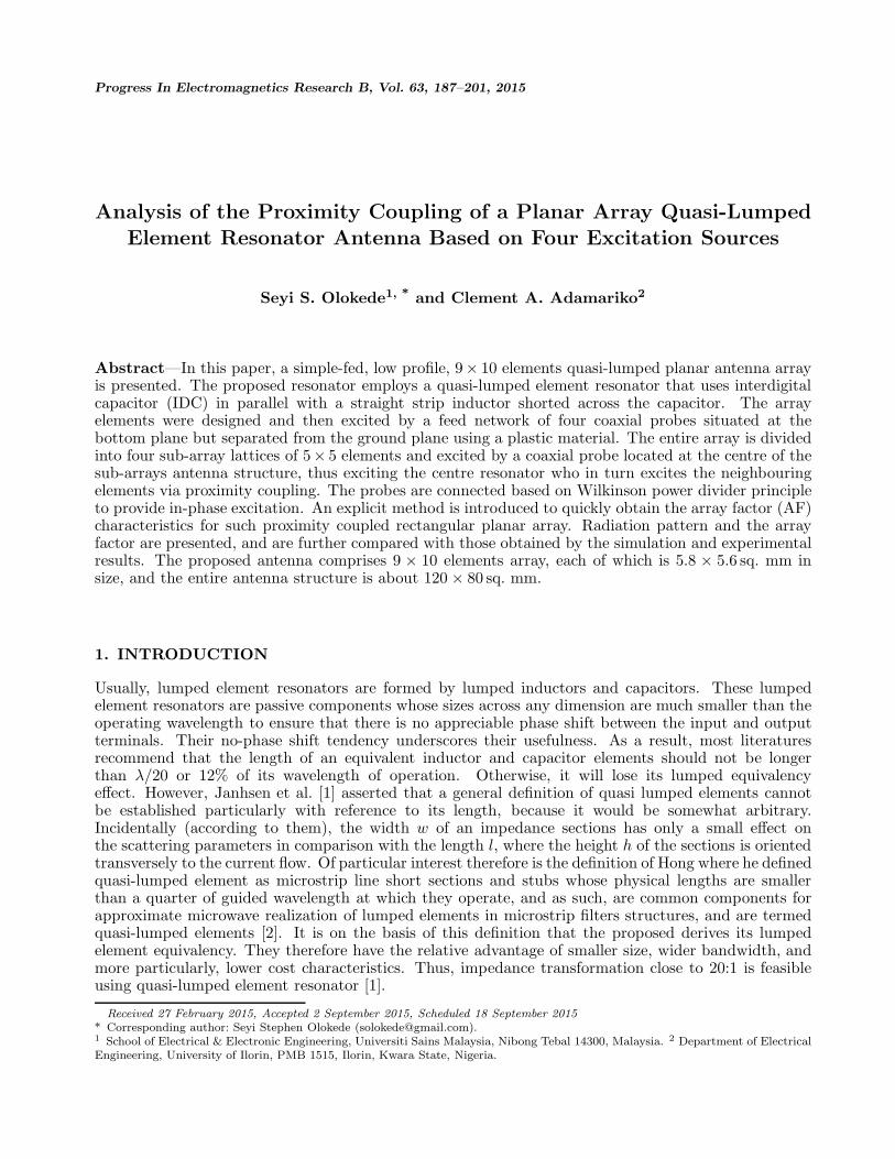
The single quasi-lumped element resonator consists of quasi-lumped microstrip line sections and stubs,which employs an interdigital finger capacitor (IDC) in parallel with a single narrow straight conductor.A meander-line inductor may also be used alternatively to improve the capacitance. The inductor (L)is the centre finger shorted across the capacitor. The pads connected at both ends of the structure actas capacitors to ground (CP ), which can be adjusted to tune the resonant frequency of the resonator.The layout of the quasi-lumped element resonator and equivalent circuit of the structure are shownin Figure 1(a). The capacitor C is an interdigital capacitor (IDC), an inductor L is the microstripinductor whereas capacitor Cp1 and Cp2 are pad capacitances. The interdigital capacitor C is a comb-like, digit-like or finger-like periodic pattern deposited on a broad types of substrates which could beporous, transparent or opaque [3]. In order to create high-Q (a figure of merit, which is a measure ofthe performance or quality of a resonator) a planar IDC is deposited on the surface of a relatively highdielectric constant substrate. The Q-factor can be enhanced by using high-conductivity conductors, low-loss tangent dielectric materials, Q-enhancement techniques including suspended substrate, multilayerstructures and macro-machining [4]. The essence of IDC is to build up the capacitance associatedwith the electric field that penetrates into the substrate. Generally, it relies on the strip-to-strip (gap)
(a) (b)
Figure 1. Quasi-lumped element resonator. (a) Subcomponent, (b) dimensioned.
Progress In Electromagnetics Research B, Vol. 63, 2015 189
capacitance of parallel conducting fingers on a substrate, and uses the capacitance that occurs across anarrow gap thin-film conductors. These gaps are essentially very long but folded to use a small amountof area, therefore compact area is obtained. In order to achieve maximum capacitance density, thefinger width (w1) must be approximately equal to inter-finger space (ge). Also, the substrate thickness(h) should be much larger than the finger width. The capacitance can be increased by increasing thenumber of fingers, using a thin layer of high dielectric material between the substrate and conductor,or using an overlay high-k [5].
In this work a moderate dielectric constant was used and the equation to determine the IDC ofthe resonator was stated by Avenhaus in [6] and also appropriately stated in Eq. (2) of [7] for the samedesign specifications and considerations, where N is the number of fingers, CL is the overlap length ofIDC fingers, and Δ = 0.5(weff −w1) (which is equal to 0.5 for this design) is the correction factor due tothe effect of fringing field. The Q-factor of an inductor depends directly on the inductance, whereas theinductor is a single narrow straight inductor shorted across the IDC as shown in Figure 1(a). Normally,when inductor is narrow, it becomes more inductive but carry less current. As such, the inductance ofa narrow strip inductor is decreased by the presence of a ground plane. Hence, an inductor width of1.2 mm can comfortably carry sufficient current, while the entire structure of length 5.8 mm is broadenough to neutralize the effect of the presence of ground plane. The inductance of the structure isdominated by the magnetic field close to the centre strip and the value is dependent on the total length,spacing, and line width. The inductance L produced by the straight inductor can be calculated byEq. (2) as stated in [8–13], and more specifically in Eq. (1) of [7] where IL is the inductor length, W1
is the inductor width, and t is the metal thickness as shown in Figure 1(b).The IDC capacitor C and the inductor L are approximately calculated on the basis of ge/h < 1
where ge is the inter finger spacing, and h is the substrate thickness. It is evident from finite integrationtechnique (FIT) analysis that the magnetic field lines do not loop around each finger but rather looparound the entire cross section of the interdigital width. Thus, the structure can be treated usingmicrostrip transmission line theory, with � as the length of the structure. The resonant frequency of theresonator is given in [12], also stated as Eq. (7) of [7] and it’s dependent on, the inductor strip L, thecapacitive inductance from the IDC (the length of the finger, the line width of the finger), and the padcapacitances, Cp where C is the IDC defined by Eq. (2) of [7], and L is the strip inductance defined byEq. (1) of [7]. Cp1 = Cp2 are pad capacitances defined by Eq. (6) of [7], and are formed between the gapsand the ground. The equation to determine the pad capacitance is also stated similarly in [13] where �is the resonator length, and h is the substrate thickness. It is noteworthy that the pad capacitances donot depend on the size and the number of fingers, but rather on the substrate thickness, the length ofthe IDC, and finally, the effective line width. Therefore, it is also not impossible to have a large value ofIDC without increasing the pad effect [14]. Essentially, the pads connected at both ends of the IDC actsas capacitor to ground with the sole aim of adjusting (tuning) the resonant frequency of the resonator,weff is the effective line width given in Eq. (2) [15] and εeff is the effective dielectric constant definedin Eq. (1).
εeff =(εr + 1)
2+
(εr − 1)2
[1 +
10hw
]−0.5
(1)
weff = w +t
πln
⎧⎪⎪⎪⎪⎪⎪⎪⎪⎪⎨⎪⎪⎪⎪⎪⎪⎪⎪⎪⎩
10.872√√√√√(
t
h
)2⎡⎣ 1
π(w
t+ 1.10
)⎤⎦
2
⎫⎪⎪⎪⎪⎪⎪⎪⎪⎪⎬⎪⎪⎪⎪⎪⎪⎪⎪⎪⎭
(2)
2.2. Problem Formulation of the Array
A planar array comprises definitely arranged finite sized identical antenna radiators which are fed byan appropriate feed network. In a way, the fields radiated from one radiator is received by the other
190 Olokede and Adamariko
radiators. Hence, the signal get reflected, re-radiated, or scattered. The properties of these signalsdepends on the power of the signal, reflection coefficients, and possibly an additional electrical phaseintroduced due to propagation delay from one element to the other. This kind of interaction between theantenna elements and hence, can alter the array characteristics. Assume therefore that a planar arrayhas m×n elements and are arranged in the xy-plane. In the x-direction, the number of array elements ism = 9, and in the y-direction the number of array is n = 10. If all the elements are fully excited by theproposed feed network, the pattern of the proposed array can be expressed as the product of the excited(actives) element factors and the array factor, in an analogous fashion to traditional array theory. Toachieve this, it is assumed that 1) the element factor, f(θ) is identical to the pattern of a single elementtaken in isolation from the array, and is the same for any element in the array; 2) the overall patternΣf(θ) obtained is called the active patterns of the array; and finally, 3) f(θ) will depend on the positionof the feed elements in the array such that edge elements will have active element patterns than theelements near the centre of the array, and for large array however, most of the elements will see auniform neighbouring environment, and eventually, f(θ) can be approximated as equal for all elementsin the array.
2.3. The Coupling Excitation
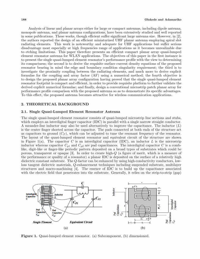
To achieve the conditions set in Section 2.2, the proposed array is fed by a feed probe network consistingof four coaxial probes located at the coordinates p1(xs, ys), p2(xs, ys), p3(xs, ys) and p4(xs, ys) to formtwo dimensional 2×2 source distribution as shown in Figure 1(a). The entire array elements were exciteddue to proximity coupling from the adjacent elements as a result of these four excitation coaxial probesto produce efficient excitation distribution. The antenna array lattice is arranged with four rectangulararray lattices of 5 × 5 each (with the fifth column doubly overlapped to form the fifth column in eachof the four lattices) and each is excited by a probe. The nodes of the array lattice are arranged inhorizontal rows and vertical columns of similar inter element spacing of λg/2, where λg is the guidedwavelength. The effective spacing between adjacent nodes in each column (dy) is 0.159λ5.8 GHz whereasthat of horizontal (dx) is 0.162λ5.8 GHz as shown in Figure 2(b). Let the planar array antenna be arrangedin a plane z = 0 as shown in the Figure 2(a), which consists of xy-plane and the xz -plane cross sections ofthe proposed rectangular planar antenna. Also, let the beam direction be determined by the coordinatesof the nodes in a periodic Cartesian in the plane of direction cosines x = sin θ sinφ and y = sin θ cos φ,where θ and φ are the angles measured at the axes z and x respectively. The excited elements (p(xs, ys))in the figure with above coordinates are referred to as line sources (otherwise known as active elementsor drivers). Consider the fact that a periodic lattice forms (m×n) nodes in the xy-plane of the Cartesian
(a) (b)
Figure 2. The array configuration. (a) The feed network, (b) the spacing.
Progress In Electromagnetics Research B, Vol. 63, 2015 191
coordinates with the polar radius of
R =[(mdx)2 + (ndy)2
]0.5 (3)
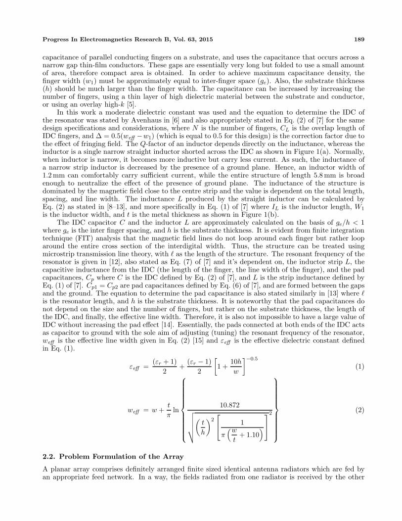
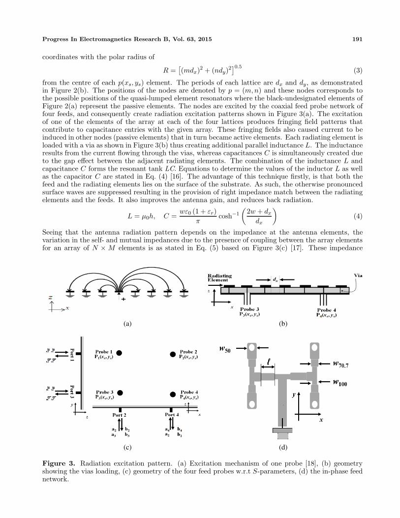
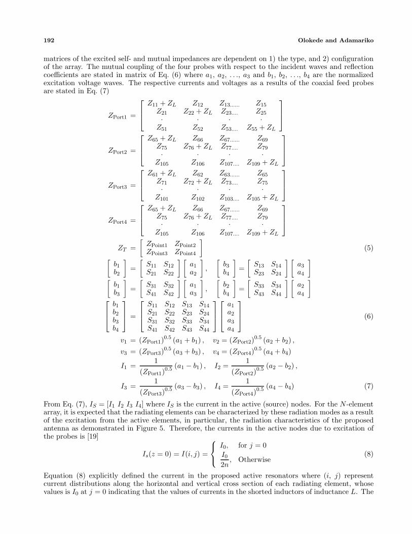
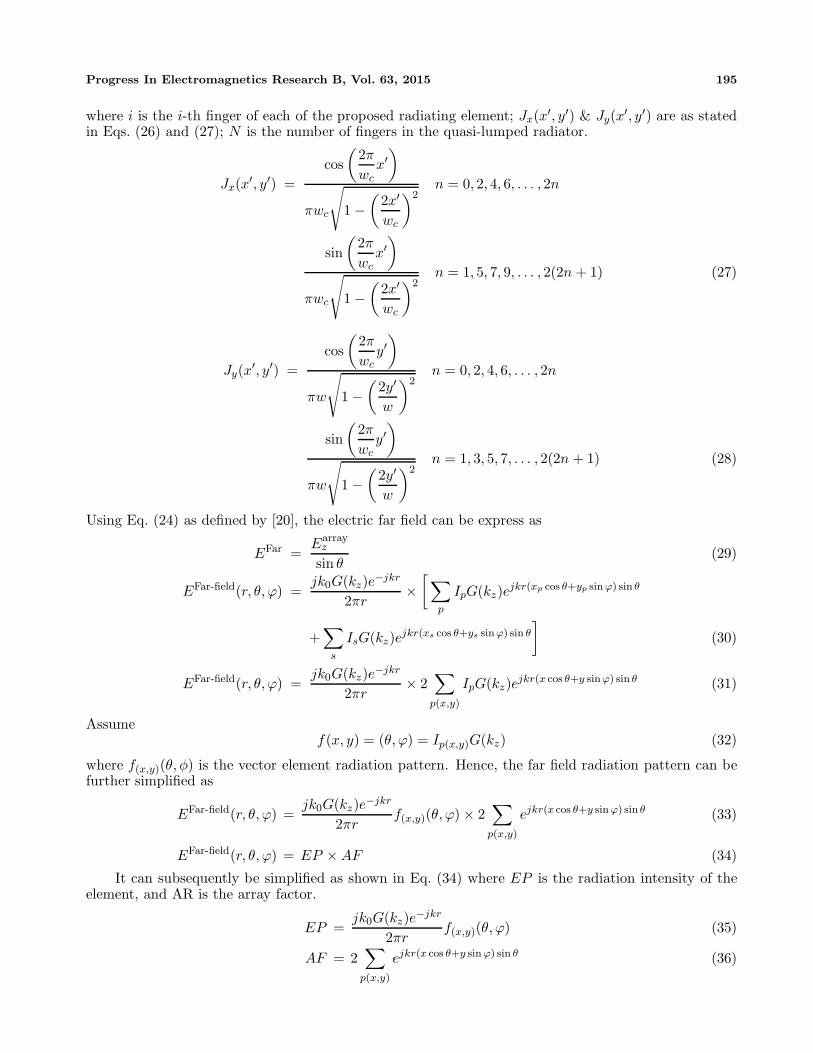
from the centre of each p(xs, ys) element. The periods of each lattice are dx and dy, as demonstratedin Figure 2(b). The positions of the nodes are denoted by p = (m,n) and these nodes corresponds tothe possible positions of the quasi-lumped element resonators where the black-undesignated elements ofFigure 2(a) represent the passive elements. The nodes are excited by the coaxial feed probe network offour feeds, and consequently create radiation excitation patterns shown in Figure 3(a). The excitationof one of the elements of the array at each of the four lattices produces fringing field patterns thatcontribute to capacitance entries with the given array. These fringing fields also caused current to beinduced in other nodes (passive elements) that in turn became active elements. Each radiating element isloaded with a via as shown in Figure 3(b) thus creating additional parallel inductance L. The inductanceresults from the current flowing through the vias, whereas capacitances C is simultaneously created dueto the gap effect between the adjacent radiating elements. The combination of the inductance L andcapacitance C forms the resonant tank LC. Equations to determine the values of the inductor L as wellas the capacitor C are stated in Eq. (4) [16]. The advantage of this technique firstly, is that both thefeed and the radiating elements lies on the surface of the substrate. As such, the otherwise pronouncedsurface waves are suppressed resulting in the provision of right impedance match between the radiatingelements and the feeds. It also improves the antenna gain, and reduces back radiation.
L = μ0h, C =wε0 (1 + εr)
πcosh−1
(2w + dx
dx
)(4)
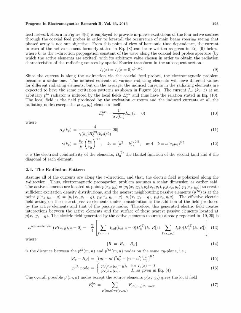
Seeing that the antenna radiation pattern depends on the impedance at the antenna elements, thevariation in the self- and mutual impedances due to the presence of coupling between the array elementsfor an array of N × M elements is as stated in Eq. (5) based on Figure 3(c) [17]. These impedance
(a) (b)
(c) (d)
Figure 3. Radiation excitation pattern. (a) Excitation mechanism of one probe [18], (b) geometryshowing the vias loading, (c) geometry of the four feed probes w.r.t S-parameters, (d) the in-phase feednetwork.
192 Olokede and Adamariko
matrices of the excited self- and mutual impedances are dependent on 1) the type, and 2) configurationof the array. The mutual coupling of the four probes with respect to the incident waves and reflectioncoefficients are stated in matrix of Eq. (6) where a1, a2, . . ., a3 and b1, b2, . . ., b4 are the normalizedexcitation voltage waves. The respective currents and voltages as a results of the coaxial feed probesare stated in Eq. (7)
ZPort1 =
⎡⎢⎣
Z11 + ZL Z12 Z13...... Z15
Z21 Z22 + ZL Z23.... Z25
· · · ·Z51 Z52 Z53.... Z55 + ZL
⎤⎥⎦
ZPort2 =
⎡⎢⎣
Z65 + ZL Z66 Z67...... Z69
Z75 Z76 + ZL Z77.... Z79
· · · ·Z105 Z106 Z107.... Z109 + ZL
⎤⎥⎦
ZPort3 =
⎡⎢⎣
Z61 + ZL Z62 Z63...... Z65
Z71 Z72 + ZL Z73.... Z75
· · · ·Z101 Z102 Z103.... Z105 + ZL
⎤⎥⎦
ZPort4 =
⎡⎢⎣
Z65 + ZL Z66 Z67...... Z69
Z75 Z76 + ZL Z77.... Z79
· · · ·Z105 Z106 Z107.... Z109 + ZL
⎤⎥⎦
ZT =[
ZPoint1 ZPoint2
ZPoint3 ZPoint4
](5)[
b1
b2
]=
[S11 S12
S21 S22
] [a1
a2
],
[b3
b4
]=
[S13 S14
S23 S24
] [a3
a4
][
b1
b3
]=
[S31 S32
S41 S42
] [a1
a3
],
[b2
b4
]=
[S33 S34
S43 S44
] [a2
a4
]⎡⎢⎣
b1
b2
b3
b4
⎤⎥⎦ =
⎡⎢⎣
S11 S12 S13 S14
S21 S22 S23 S24
S31 S32 S33 S34
S41 S42 S43 S44
⎤⎥⎦
⎡⎢⎣
a1
a2
a3
a4
⎤⎥⎦ (6)
v1 = (ZPort1)0.5 (a1 + b1) , v2 = (ZPort2)
0.5 (a2 + b2) ,
v3 = (ZPort3)0.5 (a3 + b3) , v4 = (ZPort4)
0.5 (a4 + b4)
I1 =1
(ZPort1)0.5 (a1 − b1) , I2 =
1(ZPort2)
0.5 (a2 − b2) ,
I3 =1
(ZPort3)0.5 (a3 − b3) , I4 =
1(ZPort4)
0.5 (a4 − b4) (7)
From Eq. (7), IS = [I1 I2 I3 I4] where IS is the current in the active (source) nodes. For the N -elementarray, it is expected that the radiating elements can be characterized by these radiation modes as a resultof the excitation from the active elements, in particular, the radiation characteristics of the proposedantenna as demonstrated in Figure 5. Therefore, the currents in the active nodes due to excitation ofthe probes is [19]
Is(z = 0) = I(i, j) =
⎧⎨⎩
I0, for j = 0I0
2n, Otherwise
(8)
Equation (8) explicitly defined the current in the proposed active resonators where (i, j) representcurrent distributions along the horizontal and vertical cross section of each radiating element, whosevalues is I0 at j = 0 indicating that the values of currents in the shorted inductors of inductance L. The
Progress In Electromagnetics Research B, Vol. 63, 2015 193
feed network shown in Figure 3(d) is employed to provide in-phase excitations of the four active sourcesthrough the coaxial feed probes in order to forestall the occurrence of main beam steering seeing thatphased array is not our objective. From this point of view of harmonic time dependence, the currentin each of the active element formerly stated in Eq. (8) can be re-written as given in Eq. (9) below,where kz is the z-direction propagation constant of the wave along the coaxial feed probes aperture (bywhich the active elements are excited) with its arbitrary value chosen in order to obtain the radiationcharacteristics of the radiating sources by spatial Fourier transform in the subsequent section.
Is(z) = Is(z = 0)e(−jk)z (9)Since the current is along the z-direction via the coaxial feed probes, the electromagnetic problembecomes a scalar one. The induced currents at various radiating elements will have different valuesfor different radiating elements, but on the average, the induced currents in the radiating elements areexpected to have the same excitation patterns as shown in Figure 3(a). The current Iind(kz; z) at anarbitrary pth radiator is induced by the local fields Eloc
s and thus have the relation stated in Eq. (10).The local field is the field produced by the excitation currents and the induced currents at all theradiating nodes except the p(xs, ys) elements itself.
Elocs =
1αs(kz)
Iind(z = 0) (10)
where
αs(kz) =4
γ(kz)H(2)0 (krd/2)
[20] (11)
γ(kz) =kr
k
(μ0
ε0
)0.5
, kr =(k2 − k2
z
)0.5, and k = ω(ε0μ0)0.5 (12)
σ is the electrical conductivity of the elements, H(2)0 the Hankel function of the second kind and d the
diagonal of each element.
2.4. The Radiation Pattern
Assume all of the currents are along the z-direction, and that, the electric field is polarized along thez-direction. Thus, electromagnetic propagation problem assumes a scalar dimension as earlier said.The active elements are located at point p(xs, ys) = [p1(xs, ys), p2(xs, ys), p3(xs, ys), p4(xs, ys)] to createsufficient excitation density distributions, and the nearest neighbouring passive elements (p
′th) is at thepoint p(xs, ys − g) = [p1(xs, ys − g), p2(xs, ys − g), p3(xs, ys − g), p4(xs, ysg)]. The effective electricfield acting on the nearest passive elements under consideration is the addition of the field producedby the active elements and that of the passive nodes. Therefore, this generated electric field createsinteractions between the active elements and the surface of these nearest passive elements located atp(xs, ys − g). The electric field generated by the active elements (sources) already reported in [19, 20] is
Eactive-element (P (x, y), z = 0) = −γ
4
⎡⎣ ∑
P (m,n)
Iind(kz; z = 0)H(2)0 (kr|R|)+
∑P (xs,ys)
Is(0)H(2)0 (kr|R|)
⎤⎦ (13)
where|R| = |Rs − Rs′ | (14)
is the distance between the pth(m,n) and p′th(m,n) nodes on the same xy-plane, i.e.,
|Rs − Rs′ | =[(m − m′)2d2
x + (n − n′)2d2y
]0.5 (15)
p′th node =
{ps(xs, ys − g), for Is(z) = 0ps(xs, ys), Is as given in Eq. (4) (16)
The overall possible p′(m,n) nodes except the source elements p(xs, ys) gives the local field
Elocs =
∑p′(m,n)�=p(xs,ys)
Ep′(m,y)th−node (17)

194 Olokede and Adamariko
Note that when p(xs, ys) is very close to p(xs, ys−g), the induced currents in other passive elements arequite small compared to the source element p(xs, ys). Therefore, the main contribution to the local fieldat the surface of p(xs, ys − g) element is the field radiated by each of the element source. Henceforth,
Elocs ≈ Es (xs, ys − g, z = 0) (18)
Substituting Eq. (11) into Eq. (10), and using Eq. (13), this system of linear equations are obtained forthe induced currents Iind(m,n) as∑
p(m,n)p(xs,ys)
kp(m,n)p(xs,ys−h)Iind(m,n)(kz ; z = 0) =14αs(kz)γ
∑p(xs,ys)
H(2)0 (kr|Rs|)Is(0) (19)
wherekp(m,n)p(xs,ys−h) = δp(m,n)p(xs,ys−h) + αp(m,n)γ(kz)H
(2)0 (kr|R|)/4 (20)
δi,j is the Kronecker delta function. Subsequently, the field at arbitrary point P (x, y) produced by thewhole structure can be calculated as shown in Eq. (21) below having obtained the induced currentsIind(kz; z = 0) by solving the above system of linear equations.
Eactive-element (P (x, y), z = 0) = −γ
4
⎡⎣ ∑
P (m,n)
Iind(kz; z = 0)H(2)0 (kr|R|)+
∑P (xs,ys)
Is(0)H(2)0 (kr|R|)
⎤⎦ (21)
Consider a quasi-lumped resonator sources which has the following current distributions
IS = IS(0)J(z) (22)
Therefore, the current distributions can be stated as
J(z) =
∞∫−∞
G(kz)ejkzzdkz (23)
Hence, G(kz) can be determined as stated in Eq. (24) by performing the inverse Fourier transform ofEq. (23)
G(kz) =
∞∫−∞
Jz(z)e−jkzdkz (24)
where G(kz) is the Fourier transform of the current distribution function of the radiating element sourceslocated at point p(xs, ys). It is then apparent that the z-component of the electric field at any arbitrarypoint p(x, y, z) generated by these sources can be determined by Fourier transform with respect to theparameter kz seeing the solution for a radiating source problem gives the solution for the Fourier spatialharmonic of the antenna current. Hence, the linearity of the problem allow the use of the principle ofsuperposition and as such, the electric field at any arbitrary point p(x, y, z) produced by the sources isgiven as
Ez(x, y, z) =
∞∫−∞
G(kz)EActive-element (R, z = 0) e−jkzdkz (25)
where EActive−element(R, z = 0) is the electric field produced by each of the active element sourceIS(0)ejkzz stated in Eq. (21). The said radiating active element source exhibit the current distribution
Jz(z) =N∑
i=1
[Jx(x, y) + Jy(x, y)] (26)
Progress In Electromagnetics Research B, Vol. 63, 2015 195
where i is the i-th finger of each of the proposed radiating element; Jx(x′, y′) & Jy(x′, y′) are as statedin Eqs. (26) and (27); N is the number of fingers in the quasi-lumped radiator.
Jx(x′, y′) =cos
(2πwc
x′)
πwc
√1 −
(2x′
wc
)2n = 0, 2, 4, 6, . . . , 2n
sin(
2πwc
x′)
πwc
√1 −
(2x′
wc
)2n = 1, 5, 7, 9, . . . , 2(2n + 1) (27)
Jy(x′, y′) =cos
(2πwc
y′)
πw
√1 −
(2y′
w
)2n = 0, 2, 4, 6, . . . , 2n
sin(
2πwc
y′)
πw
√1 −
(2y′
w
)2n = 1, 3, 5, 7, . . . , 2(2n + 1) (28)
Using Eq. (24) as defined by [20], the electric far field can be express as
EFar =Earray
z
sin θ(29)
EFar-field(r, θ, ϕ) =jk0G(kz)e−jkr
2πr×
[∑p
IpG(kz)ejkr(xp cos θ+yp sin ϕ) sin θ
+∑
s
IsG(kz)ejkr(xs cos θ+ys sinϕ) sin θ
](30)
EFar-field(r, θ, ϕ) =jk0G(kz)e−jkr
2πr× 2
∑p(x,y)
IpG(kz)ejkr(x cos θ+y sinϕ) sin θ (31)
Assumef(x, y) = (θ, ϕ) = Ip(x,y)G(kz) (32)
where f(x,y)(θ, φ) is the vector element radiation pattern. Hence, the far field radiation pattern can befurther simplified as
EFar-field(r, θ, ϕ) =jk0G(kz)e−jkr
2πrf(x,y)(θ, ϕ) × 2
∑p(x,y)
ejkr(x cos θ+y sin ϕ) sin θ (33)
EFar-field(r, θ, ϕ) = EP × AF (34)
It can subsequently be simplified as shown in Eq. (34) where EP is the radiation intensity of theelement, and AR is the array factor.
EP =jk0G(kz)e−jkr
2πrf(x,y)(θ, ϕ) (35)
AF = 2∑
p(x,y)
ejkr(x cos θ+y sinϕ) sin θ (36)
196 Olokede and Adamariko
where x′ = mdx, y′ = ndy, z′ = 0, k = 2π/λ, x = x′ sin θ cos φ, and y = y′ sin θ cos φ. Therefore, Eq. (34)represents the radiation pattern of the proposed array in 3-D. Hence, the radiation pattern of an arrayof N × M -identical elements evaluated at location (θ, φ) in the far-field can be approximated by theproduct of radiation intensity of the element (EP ) and the array factor (AR).
3. VALIDATION AND DESIGN SPECIFICATIONS
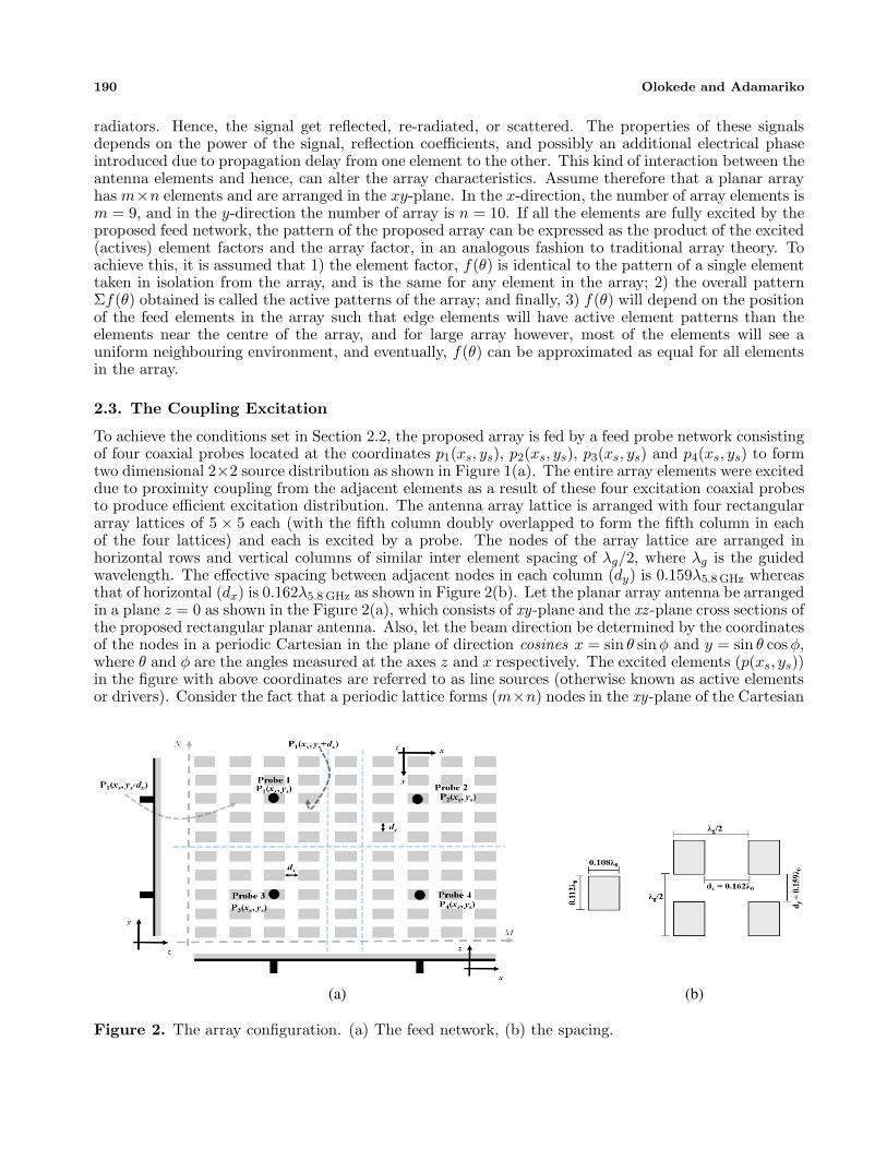
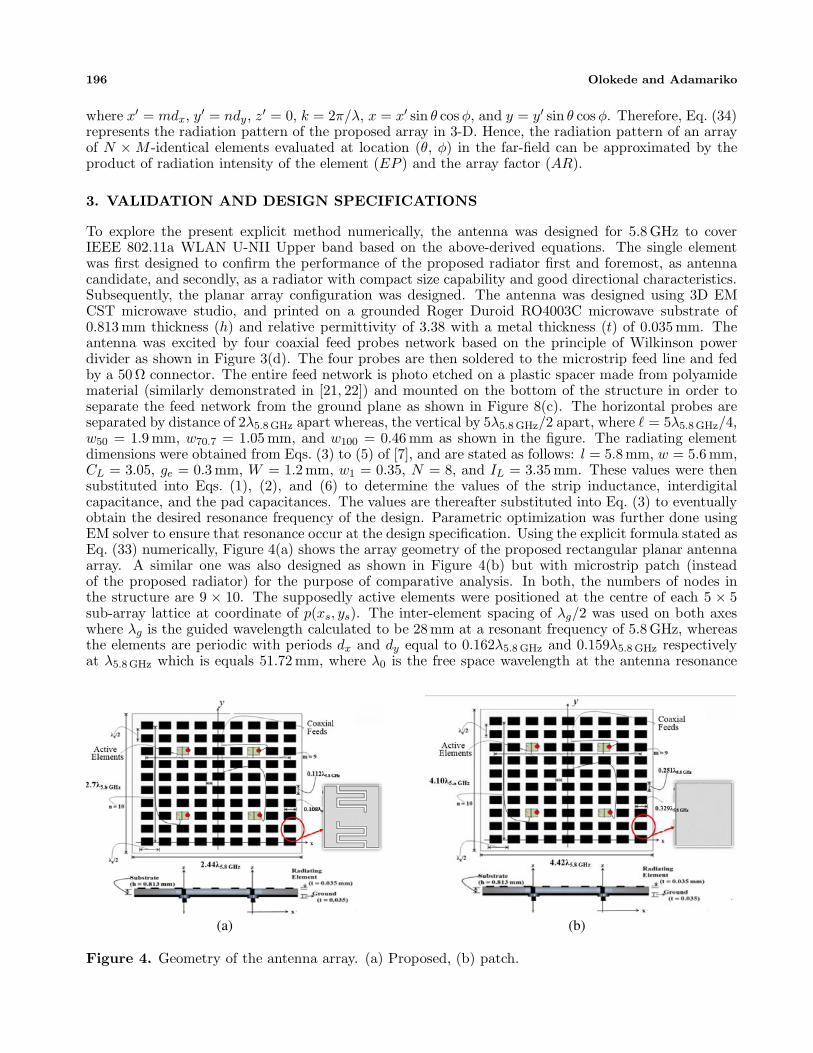
To explore the present explicit method numerically, the antenna was designed for 5.8 GHz to coverIEEE 802.11a WLAN U-NII Upper band based on the above-derived equations. The single elementwas first designed to confirm the performance of the proposed radiator first and foremost, as antennacandidate, and secondly, as a radiator with compact size capability and good directional characteristics.Subsequently, the planar array configuration was designed. The antenna was designed using 3D EMCST microwave studio, and printed on a grounded Roger Duroid RO4003C microwave substrate of0.813 mm thickness (h) and relative permittivity of 3.38 with a metal thickness (t) of 0.035 mm. Theantenna was excited by four coaxial feed probes network based on the principle of Wilkinson powerdivider as shown in Figure 3(d). The four probes are then soldered to the microstrip feed line and fedby a 50 Ω connector. The entire feed network is photo etched on a plastic spacer made from polyamidematerial (similarly demonstrated in [21, 22]) and mounted on the bottom of the structure in order toseparate the feed network from the ground plane as shown in Figure 8(c). The horizontal probes areseparated by distance of 2λ5.8GHz apart whereas, the vertical by 5λ5.8 GHz/2 apart, where � = 5λ5.8GHz/4,w50 = 1.9 mm, w70.7 = 1.05 mm, and w100 = 0.46 mm as shown in the figure. The radiating elementdimensions were obtained from Eqs. (3) to (5) of [7], and are stated as follows: l = 5.8 mm, w = 5.6 mm,CL = 3.05, ge = 0.3 mm, W = 1.2 mm, w1 = 0.35, N = 8, and IL = 3.35 mm. These values were thensubstituted into Eqs. (1), (2), and (6) to determine the values of the strip inductance, interdigitalcapacitance, and the pad capacitances. The values are thereafter substituted into Eq. (3) to eventuallyobtain the desired resonance frequency of the design. Parametric optimization was further done usingEM solver to ensure that resonance occur at the design specification. Using the explicit formula stated asEq. (33) numerically, Figure 4(a) shows the array geometry of the proposed rectangular planar antennaarray. A similar one was also designed as shown in Figure 4(b) but with microstrip patch (insteadof the proposed radiator) for the purpose of comparative analysis. In both, the numbers of nodes inthe structure are 9 × 10. The supposedly active elements were positioned at the centre of each 5 × 5sub-array lattice at coordinate of p(xs, ys). The inter-element spacing of λg/2 was used on both axeswhere λg is the guided wavelength calculated to be 28 mm at a resonant frequency of 5.8 GHz, whereasthe elements are periodic with periods dx and dy equal to 0.162λ5.8 GHz and 0.159λ5.8 GHz respectivelyat λ5.8GHz which is equals 51.72 mm, where λ0 is the free space wavelength at the antenna resonance
(a) (b)
Figure 4. Geometry of the antenna array. (a) Proposed, (b) patch.
Progress In Electromagnetics Research B, Vol. 63, 2015 197
(a) Normalized array factor (AF) (b) E-Plane (c) H-Plane
(d) E-Plane (e) H-Plane (f) E-Plane of the patch array
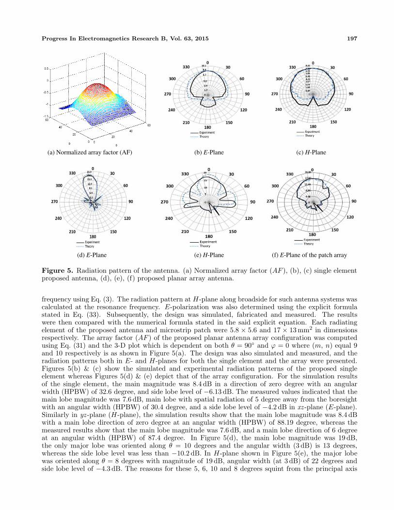
Figure 5. Radiation pattern of the antenna. (a) Normalized array factor (AF ), (b), (c) single elementproposed antenna, (d), (e), (f) proposed planar array antenna.
frequency using Eq. (3). The radiation pattern at H-plane along broadside for such antenna systems wascalculated at the resonance frequency. E-polarization was also determined using the explicit formulastated in Eq. (33). Subsequently, the design was simulated, fabricated and measured. The resultswere then compared with the numerical formula stated in the said explicit equation. Each radiatingelement of the proposed antenna and microstrip patch were 5.8 × 5.6 and 17 × 13 mm2 in dimensionsrespectively. The array factor (AF ) of the proposed planar antenna array configuration was computedusing Eq. (31) and the 3-D plot which is dependent on both θ = 90◦ and ϕ = 0 where (m, n) equal 9and 10 respectively is as shown in Figure 5(a). The design was also simulated and measured, and theradiation patterns both in E- and H-planes for both the single element and the array were presented.Figures 5(b) & (c) show the simulated and experimental radiation patterns of the proposed singleelement whereas Figures 5(d) & (e) depict that of the array configuration. For the simulation resultsof the single element, the main magnitude was 8.4 dB in a direction of zero degree with an angularwidth (HPBW) of 32.6 degree, and side lobe level of −6.13 dB. The measured values indicated that themain lobe magnitude was 7.6 dB, main lobe with spatial radiation of 5 degree away from the boresightwith an angular width (HPBW) of 30.4 degree, and a side lobe level of −4.2 dB in xz -plane (E-plane).Similarly in yz -plane (H-plane), the simulation results show that the main lobe magnitude was 8.4 dBwith a main lobe direction of zero degree at an angular width (HPBW) of 88.19 degree, whereas themeasured results show that the main lobe magnitude was 7.6 dB, and a main lobe direction of 6 degreeat an angular width (HPBW) of 87.4 degree. In Figure 5(d), the main lobe magnitude was 19 dB,the only major lobe was oriented along θ = 10 degrees and the angular width (3 dB) is 13 degrees,whereas the side lobe level was less than −10.2 dB. In H-plane shown in Figure 5(e), the major lobewas oriented along θ = 8 degrees with magnitude of 19 dB, angular width (at 3 dB) of 22 degrees andside lobe level of −4.3 dB. The reasons for these 5, 6, 10 and 8 degrees squint from the principal axis
198 Olokede and Adamariko
as demonstrated in Figures 5(d)–(f) is as a result of spacing differential between the horizontal andvertical periods (dy − dx) which is equals to 0.159λ5.8 GHz − 0.162λ5.8 GHz of the array. Comparing theexplicit numerical result with the simulation and experimental results demonstrates to a large extent, areasonable degree of agreement, though with minor discrepancies particularly as shown in Figure 5(e).The reason for this dissimilarity is not unconnected with the inability to precisely locate the excitationfeeds positions during fabrication with respect to the simulated feed positions. In both, one major mainlobe is observed, whereas a side-lobe level of −10.2 dB is noticed in both the simulated and experimentalresults particularly in xz -plane. Figure 5(f) shows the Eθ component radiated by a rectangular arrayin the plane cut by ϕ = 0 of the microstrip patch antenna, where the major lobe is oriented along 5degrees. The antenna beamwidth (HPBW) is 41 degrees with a side lobe level of −13.4 dB. However, aminor level of back lobe is formed in the lower part of the hemisphere which may be due to the existenceof radiations from the surrounding objects. Generally, the radiation patterns of the antennas obtainedare close to a directional type, and the beam width of the proposed antenna is 31.7% narrower thanthe patch antenna. The radiation pattern of the antenna is acceptable, and there is a good agreementbetween the theory and the measured results.
Comparing the radiation pattern of the proposed shown in Figure 4(a) with the patch antenna ofFigure 4(b) shown in Figure 5 (and in particular Figures 5(c) & (d) indicates that the proposed E-planeradiation pattern exhibits a narrow beamwidth of about 13 degree compared to the 41 degree widthexhibited by the patch with a beamwidth differential of about 28 degree. However, the patch antennaexhibited a lower sidelobe level differential of about 3 dB. The orientation of the major lobe of theE-plain pattern away from boresight as shown in Figure 5(d), as well as the major lobe E-plain squintwas investigated to determine the cause. It was discovered that the vertical spacing dy is 0.159λ5.8 GHz
(which is equal to 4.45 mm) whereas that of horizontal (dx) is 0.162λ5.8 GHz(= 4.54 mm) as shown in thefigure. The overall spacing distance of λ/2 is employed to ensure that the spacing is not greater thanλ/2. If it does, multiple maximal of equal magnitude can be formed. To avoid grating lobes in x-z andy-z planes of rectangular array, the spacing between elements should in x and y-directions respectivelymust be less than λ/2. This is the very reason why the entire spacing is λ/2 whereas, the differentialspacing on both directions are [dy is 0.159λ5.8 GHz & (dx) is 0.162λ5.8 GHz].
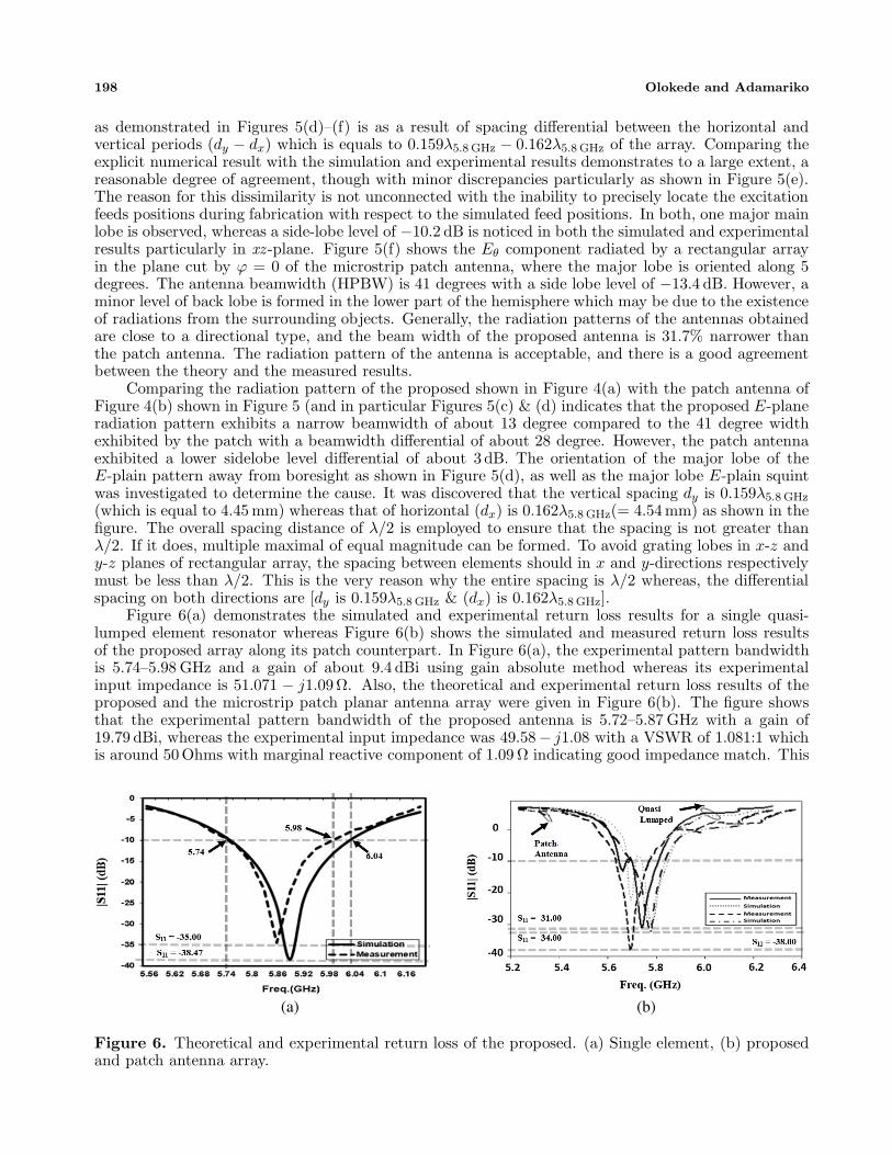
Figure 6(a) demonstrates the simulated and experimental return loss results for a single quasi-lumped element resonator whereas Figure 6(b) shows the simulated and measured return loss resultsof the proposed array along its patch counterpart. In Figure 6(a), the experimental pattern bandwidthis 5.74–5.98 GHz and a gain of about 9.4 dBi using gain absolute method whereas its experimentalinput impedance is 51.071 − j1.09Ω. Also, the theoretical and experimental return loss results of theproposed and the microstrip patch planar antenna array were given in Figure 6(b). The figure showsthat the experimental pattern bandwidth of the proposed antenna is 5.72–5.87 GHz with a gain of19.79 dBi, whereas the experimental input impedance was 49.58− j1.08 with a VSWR of 1.081:1 whichis around 50 Ohms with marginal reactive component of 1.09 Ω indicating good impedance match. This
(a) (b)
Figure 6. Theoretical and experimental return loss of the proposed. (a) Single element, (b) proposedand patch antenna array.
Progress In Electromagnetics Research B, Vol. 63, 2015 199
is supported by Figure 7 which shows the simulated and measured voltage standing wave ratio (VSWR)of the proposed and the patch array antennas.
The area occupied by the proposed antenna can be determined by Eqs. (37) and (38).
A(x, y) =
m=9∫xi
n=10∫yi
A(xi, yi)(x, y)dxdy (37)
A(x, y) =m=9∑xi
n=10∑yi
[(lyi + 0.159) (bxi + 0.162)] (38)
where ly and bx are the length and breadth of the radiating elements respectively. Using Figure 2(a),the length and breadth of the proposed is determined by
ly(x, y) = (0.112 + 0.159)λ5.8 GHz × 10 = 2.71λ5.8 GHz
bx(x, y) = (0.108 + 0.162)λ5.8 GHz × 9 = 2.43λ5.8 GHz
and thus the area can be stated as 2.71λ5.8 GHz × 2.43λ5.8 GHz. Hence, the estate area of the patch can
Figure 7. Theoretical and experimental voltage standing wave ratio.
(a) (b) (c)
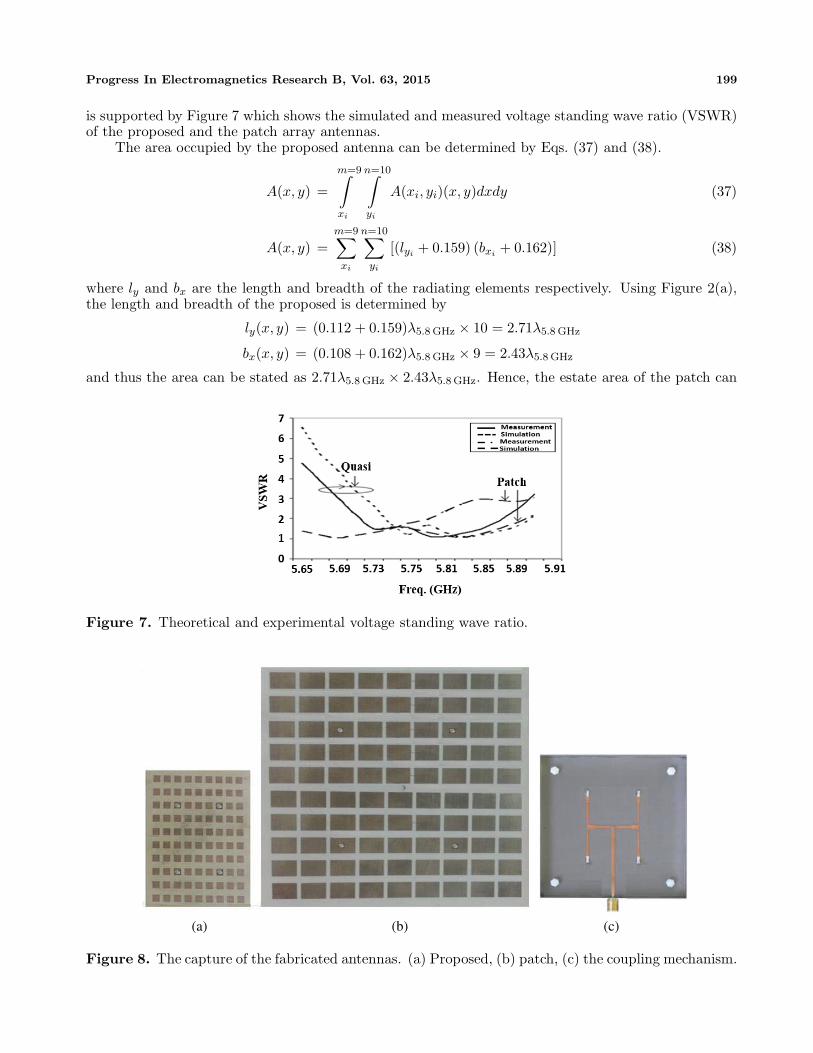
Figure 8. The capture of the fabricated antennas. (a) Proposed, (b) patch, (c) the coupling mechanism.
200 Olokede and Adamariko
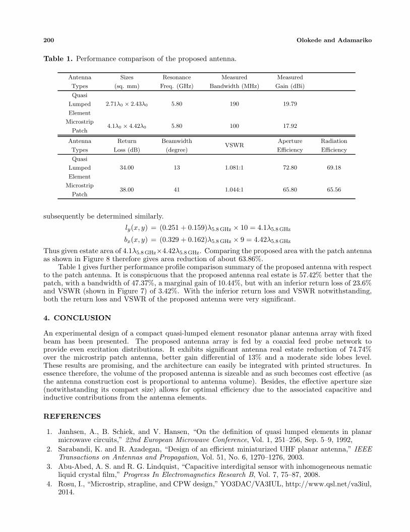
Table 1. Performance comparison of the proposed antenna.
Antenna
Types
Sizes
(sq. mm)
Resonance
Freq. (GHz)
Measured
Bandwidth (MHz)
Measured
Gain (dBi)
Quasi
Lumped
Element
2.71λ0 × 2.43λ0 5.80 190 19.79
Microstrip
Patch4.1λ0 × 4.42λ0 5.80 100 17.92
Antenna
Types
Return
Loss (dB)
Beamwidth
(degree)VSWR
Aperture
Efficiency
Radiation
Efficiency
Quasi
Lumped
Element
34.00 13 1.081:1 72.80 69.18
Microstrip
Patch38.00 41 1.044:1 65.80 65.56
subsequently be determined similarly.
ly(x, y) = (0.251 + 0.159)λ5.8 GHz × 10 = 4.1λ5.8 GHz
bx(x, y) = (0.329 + 0.162)λ5.8 GHz × 9 = 4.42λ5.8 GHz
Thus given estate area of 4.1λ5.8 GHz×4.42λ5.8 GHz. Comparing the proposed area with the patch antennaas shown in Figure 8 therefore gives area reduction of about 63.86%.
Table 1 gives further performance profile comparison summary of the proposed antenna with respectto the patch antenna. It is conspicuous that the proposed antenna real estate is 57.42% better that thepatch, with a bandwidth of 47.37%, a marginal gain of 10.44%, but with an inferior return loss of 23.6%and VSWR (shown in Figure 7) of 3.42%. With the inferior return loss and VSWR notwithstanding,both the return loss and VSWR of the proposed antenna were very significant.
4. CONCLUSION
An experimental design of a compact quasi-lumped element resonator planar antenna array with fixedbeam has been presented. The proposed antenna array is fed by a coaxial feed probe network toprovide even excitation distributions. It exhibits significant antenna real estate reduction of 74.74%over the microstrip patch antenna, better gain differential of 13% and a moderate side lobes level.These results are promising, and the architecture can easily be integrated with printed structures. Inessence therefore, the volume of the proposed antenna is sizeable and as such becomes cost effective (asthe antenna construction cost is proportional to antenna volume). Besides, the effective aperture size(notwithstanding its compact size) allows for optimal efficiency due to the associated capacitive andinductive contributions from the antenna elements.
REFERENCES
1. Janhsen, A., B. Schiek, and V. Hansen, “On the definition of quasi lumped elements in planarmicrowave circuits,” 22nd European Microwave Conference, Vol. 1, 251–256, Sep. 5–9, 1992,
2. Sarabandi, K. and R. Azadegan, “Design of an efficient miniaturized UHF planar antenna,” IEEETransactions on Antennas and Propagation, Vol. 51, No. 6, 1270–1276, 2003.
3. Abu-Abed, A. S. and R. G. Lindquist, “Capacitive interdigital sensor with inhomogeneous nematicliquid crystal film,” Progress In Electromagnetics Research B, Vol. 7, 75–87, 2008.
4. Rosu, I., “Microstrip, strapline, and CPW design,” YO3DAC/VA3IUL, http://www.qsl.net/va3iul,2014.

Progress In Electromagnetics Research B, Vol. 63, 2015 201
5. Bahl, I., Lumped Element for RF and Microwave Circuits, Artech House, 2003.6. Avenhaus, B., “Characterization of high temperature superconducting thin films and their
microwave application,” PhD Thesis, Faculty of Engineering, University of Birmingham, Sep. 1996.7. Ain, M. F., S. S. Olokede, Y. M. Qasaymeh, A. Marzuki, J. J. Mohammed, S. Srimala,
S. D. Hutagalung, Z. A. Ahmad, and M. Z. Abdulla, “A novel 5.8 GHz quasi-lumped elementresonator antenna,” Int. J. Electron. Commun. (AEU), Vol. 67, 557–563, 2013.
8. Huang, F., B. Avenhaus, and M. J. Lancaster, “Lumped-element switchable superconductingfilters,” IEE Proc. Microwave on Antennas Propag., Vol. 146, No. 3, 299–233, 1999.
9. Wadell, B. C., Transmission Line Design Handbook, Artech House, Boston, 1991.10. Su, H. T., F. Huang, and M. J. Lancaster, “Compact pseudo-lumped element quasi-elliptic filters,”
IEE Colloquium on Microwave Filters and Multiplexers, No. 2000/117, Nov. 2000.11. Bogatin, E., “Design rule for microstrip capacitance,” IEEE Trans. on Components, Hybrids and
Manufacturing, Vol. 11, 253–259, Sep. 1988.12. Yin, X.-C., C.-L. Ruan, C.-Y. Ding, and J.-H. Chu, “A compact ultra-wideband microstrip antenna
with multiple notches,” Progress In Electromagnetics Research, Vol. 84, 321–332, 2008.13. Hong, J.-S., Microstrip Filters for RF/Microwave Applications, Wiley Inter Sciences, John Wiley
& Sons, Hoboken, N. J., Jan. 6, 2011.14. Naghed, M. and I. Wolf, “Equivalent capacitances of coplanar waveguide discontinuities and
interdigitated capacitors using a three-dimension finite difference method,” IEEE Trans. onMicrowave Theory and Techniques, Vol. 38, No. 12, 1808–1815, 1990.
15. Wheeler, H. A., “Transmission-line properties of a strip line between parallel planes,” IEEE Trans.on Microwave Theory and Techniques, Vol. 26, No. 11, 866–876, 1978.
16. Gao, Y. X., K. M. Luk, and K. W. Leung, “Mutual coupling between rectangular dielectricresonator antenna by FDTD,” Proc. Inst. Elect. Eng.-Microwave Antennas Propagation, Vol. 146,No. 4, 292–294, Aug. 1999.
17. Gupta, I. J. and A. A. Kseinski, “Effect of mutual coupling on the performance of adaptive arrays,”IEEE Transactions on Antennas and Propagation, Vol. 31, No. 5, 785–791, 1983.
18. Mamishev, A. V., K. Sundara-Rajan, F. Yang, and Y. Du, “Interdigital sensors and transducers,”Proceedings of the IEEE, Vol. 92, No. 5, 808–845, May 2004.
19. He, S., C. R. Simosvki, and M. Popov, “An explicit and efficient method for obtaining the radiationcharacteristics of wire antennas in metallic photonic band gap structures,” Microwave and OpticalTech. Letters, Vol. 26, No. 2, 67–73, 2000.
20. Simosvki, C. R. and S. He, “Antennas based on modified metallic photonic band gap structuresconsisting of capacitively loaded wires,” Microwave and Optical Tech. Letters, Vol. 31, No. 3, 214–221, 2001.
21. Drossos, G., Z. Wu, and L. E. Davis, “Four-element planar arrays employing probe-fed cylindricaldielectric resonator antennas,” Microwave and Optical Tech. Letters, Vol. 18, No. 5, 315–319,Aug. 1998.
22. Bartyzal, J., T. Bostik, P. Kavacs, T. Mikulaseky, J. Puskely, Z. Randa, L. Slama, J. Vorek,and D. Wolansky, “Antenna arrays for tactical communication systems: A comparative study,”Radioengineering, Vol. 20, No. 4, 817–827, Dec. 2011.


![Global dynamics of Planar Quintic Quasi{homogeneous Di erential … · 2016-08-11 · [ Aziz, Llibre & Pantazi, Adv. Math., 2014] characterized the centers of the QHS of degree 3](https://img.pdfslide.us/doc/110x75/5f956fb80ceccb2cbc41cda4/global-dynamics-of-planar-quintic-quasihomogeneous-di-erential-2016-08-11-aziz.jpg)


![QUASI-BIGEBRES DE LIE ET ALGEBRES QUASI-BATALIN ...streaming.ictp.it/preprints/P/99/174.pdf3 Quasi-bigebres de Lie Les quasi-bigebres de Lie [6] (appelees quasi-bigebres jacobiennes](https://img.pdfslide.us/doc/110x75/60aa5fd4a787df4f051abfc1/quasi-bigebres-de-lie-et-algebres-quasi-batalin-3-quasi-bigebres-de-lie-les.jpg)