Embed Size (px)
Citation preview
Linköping Studies in Science and Technology
Dissertations, No. 1618
Analysis and Design of
DLL-Based Frequency Synthesizers for
Ultra-Wideband Communication
Amin Ojani
Department of Electrical Engineering
Linköping University, SE‒581 83 Linköping, Sweden
Linköping 2014
ISBN 978‒91‒7519‒248‒2
ISSN 0345‒7524
ii
Analysis and Design of DLL-Based Frequency Synthesizers for Ultra-Wideband
Communication
Amin Ojani
Copyright © Amin Ojani, 2014
ISBN: 978‒91‒7519‒248‒2
Linköping Studies in Science and Technology
Dissertations, No. 1618
ISSN: 0345‒7524
Division of Electronic Devices
Department of Electrical Engineering
Institute of Technology
Linköping University
SE-581 83 Linköping
Sweden
Cover image:
The cover image illustrates a sine-shaped “wordle” of the thesis.
Printed by LiU-Tryck, Linköping University
Linköping, Sweden, 2014
iii
Abstract
Ever increasing demand for high speed transmission of large data between the
electronic devices within a wireless personal area network has been motivating the
development of the appropriate wireless standards. Ultra-wideband (UWB)
communication employs the unlicensed frequency spectrum of 3.1 ‒ 10.6 GHz and
utilizes a low average transmit power to offer the potential for high data rates in short
range wireless links. WiMedia specification for UWB employs a frequency hopping
scheme which requires a very fast hopping speed of 9.47 ns. Also, the strong interferers
from the coexisting wireless technologies put stringent requirements on synthesizer’s
sideband spurs. Satisfying such challenging requirements using conventional frequency
synthesis approaches is impractical and demands for exploration, analysis and design of
new synthesizer architectures.
Essential characteristics of a delay-locked loop (DLL), such as its first-order loop
stability, relatively wide loop bandwidth, and low jitter accumulation, make DLL-based
architectures attractive candidates for fast switching and low phase noise frequency
synthesis applications. However, as an edge-combiner (EC) is required to produce
different frequencies than that of the reference clock, any misalignment in equally-
spaced DLL output edges will generate an erroneous periodicity, resulting in reference
sideband spurs at the output spectrum of the frequency synthesizer.
This thesis investigates the opportunities and challenges of employing DLL-based
architectures to synthesize carrier frequencies for wireless applications, specifically
UWB communication. The dissertation has contributed to two aspects of the topic;
mathematical modeling and analysis, as well as circuit design and implementation.
A comprehensive behavioral model of the harmonic spur levels in edge-combining
DLL-based frequency synthesizers is developed which includes the effects of the stage-
delay mismatch, the static phase error of the locked-loop, and the duty cycle distortion
iv
of the reference clock. Utilizing Fourier series representation of the DLL output phases,
an analytical expression for synthesizer’s spur levels is derived. Applying Taylor series
approximations and moment methods to the analytical formula, closed-form expressions
are obtained for the probability density function and mean value of the harmonic spur
magnitudes. Finally, a Monte Carlo-free spur-aware design flow is introduced which
significantly accelerates the iterative design procedure of the synthesizer. Accuracy and
robustness of the prediction method against wide-range values of the non-idealities are
investigated and verified through Monte Carlo simulations of the synthesizer’s
behavioral and transistor-level model in a 65-nm CMOS process.
Three DLL-based architectures are developed and designed. In the first architecture,
fast hopping frequency synthesis is achieved by introducing an open-loop compensation
technique to keep the total delay-length of the delay line unchanged at the instant of
band hopping. The relation between the compensation accuracy and the hopping speed
is analyzed and formulated. In addition, to make the technique immune to process-
voltage-temperature (PVT) variations, two calibration techniques are introduced.
Furthermore, injection-locking technique is employed to reduce the total current
consumption in the EC. The presented concept is supported by measurement results on
a test chip implemented in a 65-nm CMOS process and achieves a worst-case sideband
spur of ‒44 dBc and dissipates 21 mW of power at 1.2 V supply voltage.
The second DLL-based synthesizer employs the concept of track-and-hold (T/H)
technique to sample the lock control voltages and store them across the corresponding
capacitors during a start-up phase. In normal operation, the loop control voltage is pre-
charged to the corresponding stored voltage to perform fast channel switching. Since the
presented architecture does not rely on the DLL bandwidth for fast switching, the
existing tradeoff in phase-locked systems between the settling time and the control
voltage ripples (which result in sideband spurs) is eliminated. Also, the delay line can
be biased in low gain regions of its transfer function to reduce its noise amplification.
The third DLL-based architecture merges the edge-combing and upconversion
operations to achieve a low-power direct conversion IQ modulator based on sub-
harmonic passive mixers and multiphase duty-cycled LO. The novelty of the
architecture is in employing a quadrature mixer array in such a configuration that the
upconversion of the baseband signal can be performed at a sub-harmonic of the LO.
Therefore, the requirements on the frequency synthesizer circuitries and LO buffers are
relaxed. In addition, since rail-to-rail clocks are provided easier at such low sub-
harmonic frequencies, passive mixers are employed to further reduce the power
dissipation and improve the linearity of the overall transmitter. Multiphase sub-
harmonic LO clocks required by the proposed scheme are provided using a quadrature
edge-combining DLL.
v
Sammanfattning
Ständigt ökade krav på höghastighets dataöverföring mellan elektroniska enheter inom
ett personligt nät (personal area network, PAN) har motiverat utvecklingen av lämpliga
trådlösa standarder. Ultrabredbands (ultra-wideband, UWB) kommunikation utnyttjar
det olicensierade frekvensspektrumet 3.1 – 10.6 GHz och använder låg genomsnittlig
sändningseffekt för att kunna ge höga datatakter för trådlösa kortdistans länkar.
WiMedias specification av UWB använder ett frekvenshoppande schema som kräver
väldigt snabba hoppningstider, under 9.47 ns. Även starka interferenser från befintliga
trådlösa tekniker ställer hårda krav på de oönskade tonerna i sidobanden. Att
tillfredsställa dessa utmanande krav med konventionella frekvenssyntes metoder är
opraktiskt och kräver utforskande, analys och design av nya syntentiserararkitekturer.
Grundläggande karaktäristik för fördröjningslåsta loopar (delay-locked-loop, DLL)
karaktäristik som dess första ordningens loop stabilitet, relativt bred loop bandbredd och
låg jitter ackumulering, gör DLL baserade arkitekturer till attraktiva kandidater för
snabbväxlande frekvenssyntetiserare med lågt fasbrus. Dock, eftersom en flank-
kombinerare (edge-combiner, EC) krävs för att skapa andra frekvenser än
referensklockans, så skapar minsta obalans av de jämt fördelade flankerna från DLL:n
en felaktig periodicitet som ger övertoner i spektrumet från EC DLL baserade
frekvenssyntetiserare.
Den här avhandlingen undersöker möjligheterna och utmaningarna i att använda
DLL baserade arkitekturer för att syntetisera bärfrekvensen i trådlösa applikationer,
speciellt för UWB kommunikation. Den presenterade forskningen har bidragit i två
aspekter till området; matematisk modellering och analys, samt design och
implementation.
En omfattande beteendemodell av övertonernas amplitud i EC DLL baserade
frekvenssyntetiserare utvecklas och innehåller effekterna av skillnaderna i stegens
vi
fördröjning, statiska fasfel orsakade av den låsta slingan samt pulsbreddsdistorsioner av
referensklockan. Genom fourierserie representation av DLL:ns utfaser så härleds ett
analytiskt uttryck för syntetiserarens övertoners amplituder. Med hjälp av taylorserie
approximation och momentprincipen så fås ett uttryck på sluten form fram för
täthetsfunktionen och medelvärdet av övertonernas amplitud. Slutligen så introduceras
ett Monte Carlo fritt design flöde som tar hänsyn till de oönskade tonerna vilket
signifikant snabbar upp design processen av syntetiseraren. Precisionen och robustheten
av metoden undersöks över en stor mängd värden av oidealiteter och verifieras genom
Monte Carlo simuleringar av syntetiserarens beteende- och transistornivå modeller i en
standard 65-nm CMOS process.
Tre DLL baserade arkitekturer har utvecklats och designats. I den första arkitekturen
så möjliggörs de snabba hoppningarna av ett kompenseringsschema med öppen styrning
som håller den totala fördröjningen av fördröjnings slingan oförändrad under
bandhoppningen. Relationen mellan kompensationens precision och hoppnings
hastigheten är analyserad och formulerad. Dessutom, för att göra tekniken mer immun
mot process-spännings-temperatur (PVT) variationer, så introduceras två
kalibreringstekniker. Vidare används “injection-locking” för att reducera den totala
strömförbrukningen i EC:n. Det presenterade konceptet stöds utav mätningsresultaten
av ett testchip implementerat i 65-nm CMOS som dämper de oönskade sidobands toner
till ‒44 dBc och förbrukar 21 mW vid 1.2 V spännings.
Den andra DLL baserade syntetiseraren använder konceptet följ-och-lås (track-and-
hold) för att spara kontrollspänningar över kondensatorer under en startfas. Sedan under
normal operation så förladdas kontrollspänningarna till det sparade värdet för att
möjliggöra snabba kanalväxlingar. Eftersom den presenterade arkitekturen inte förlitar
sig på DLL:ns bandbredd för de snabba växlingarna så elimineras den befintliga
avvägningen mellan insvängningstid och kontrollspänningsrippel (vilket resulterar i
oönskade sidobands toner). Utöver det så kan fördröjningselementen ställas in till en låg
förstärkning vilket reducerar bruset.
Den tredje DLL baserade arkitekturen använder både en EC och uppkonvertering för
att åstadkomma en lågeffekts direktkonverterings IQ-modulator baserad på en flerfas,
icke 50 procentig klockpulsbredd, subharmonisk passiv mixer. Det nya med
arkitekturen är användandet av en kvadratur mixer matris konfigurerad så att
uppkonverteringen av basbandssignalen kan göras med en underton av den lokala
oscillatorn, LO. Därför blir kraven reducerade både för frekvenssyntetiseraren och för
LO buffrarna. Utöver det så har klockor med en utsignal som sträcker sig från
matningsskenan till jordskenan lättare att implementera i låga frekvenser, det möjliggör
användningen av passiva mixers vilket ytterliggare minskar effektförbrukningen samt
ökar linjäriteten för hela sändaren. De flerfas subharmoniska LO klockor som krävs för
det föreslagna schemat kommer ifrån en kvadratur edge-combining DLL.
vii
Preface
This dissertation presents my research during the period February 2009 ‒ August 2014
at the Division of Electronic Devices, Department of Electrical Engineering, Linköping
University, Sweden. The Doctoral degree comprises 80% of full-time studies including
course work and research, plus 20% of full-time teaching duties. This thesis is mainly
based on the following peer-reviewed IEEE journal articles and conference publications
which are covered in Chapters 5 ‒ 10:
Paper 1 ‒ Amin Ojani, Behzad Mesgarzadeh, and Atila Alvandpour, “Modeling
and Analysis of Harmonic Spurs in DLL-Based Frequency Synthesizers,” IEEE
Transactions on Circuits and Systems I: Regular Papers (TCAS-I), vol. PP, no. 99,
pp. 1‒10, Jun. 2014.
Paper 2 ‒ Amin Ojani, Behzad Mesgarzadeh, and Atila Alvandpour, “Monte
Carlo-Free Prediction of Spurious Performance for ECDLL-Based Synthesizers,”
IEEE Transactions on Circuits and Systems I: Regular Papers (TCAS-I), Accepted
for Publication, Aug. 2014, DOI: 10.1109/TCSI.2014.2347231.
Paper 3 ‒ Amin Ojani, Behzad Mesgarzadeh, and Atila Alvandpour, “A DLL-
Based Injection-Locked Frequency Synthesizer for WiMedia UWB,” IEEE
International Symposium on Circuits and Systems (ISCAS), Seoul, South Korea,
May 2012, pp. 2027‒2030.
Paper 4 ‒ Amin Ojani, Behzad Mesgarzadeh, and Atila Alvandpour, “A Process
Variation Tolerant DLL-Based UWB Frequency Synthesizer,” 55th IEEE
viii
International Midwest Symposium on Circuits and Systems (MWSCAS), Boise, ID,
USA, Aug. 2012, pp. 558‒561.
Paper 5 ‒ Amin Ojani, Behzad Mesgarzadeh, and Atila Alvandpour, “A
Quadrature UWB Frequency Synthesizer with Dynamic Settling-Time
Calibration,” IEEE International Symposium on Circuits and Systems (ISCAS),
Beijing, China, May 2013, pp. 2480‒2483.
Paper 6 ‒ Amin Ojani, Behzad Mesgarzadeh, and Atila Alvandpour, “A 65-nm
CMOS UWB Frequency Synthesizer,” Manuscript to be Submitted for Publication.
Paper 7 ‒ Amin Ojani, Behzad Mesgarzadeh, and Atila Alvandpour, “A Self-
Calibration Technique for Fast-Switching Frequency-Hopped UWB Synthesis,”
21th IEEE International Conference Mixed Design of Integrated Circuits and
Systems (MIXDES), Lublin, Poland, Jun. 2014, pp. 154‒159.
Paper 8 ‒ Amin Ojani, Behzad Mesgarzadeh, and Atila Alvandpour, “A Low-
Power Direct IQ Upconversion Technique Based on Duty-Cycled Multi-Phase Sub-
Harmonic Passive Mixers for UWB Transmitters,” IEEE International Symposium
on Integrated Circuits (ISIC), Singapore, Dec. 2014.
The following paper was also published during this period which falls outside the scope
of this thesis:
Sima Payami and Amin Ojani, “An Operational Amplifier for High-Performance
Pipelined ADCs in 65nm CMOS,” 30th IEEE Norchip, Copenhagen, Denmark, pp.
1‒4, Nov. 2012.
ix
Contributions
The main contributions of this dissertation are as follows:
Development of a comprehensive behavioral model of harmonic spurs in edge-
combining DLL-based frequency synthesizers, which includes the effects of delay
mismatch, static phase error, and duty cycle distortion.
Development of an analytical model for mathematical formulation of spur-to-
carrier ratio at synthesizer’s output spectrum.
Development of a generic prediction model for estimation of synthesizer’s spurious
performance based on closed-form expressions.
Development of a spur-aware Monte Carlo-free design flow to accelerate the
iterative design procedure of edge-combining DLL-based frequency synthesizers.
Design and implementation of a fast hopping DLL-based frequency synthesizer for
UWB communication in a 65-nm CMOS technology, along with the design of two
calibration techniques to compensate the effect of PVT variations on synthesizer’s
hopping speed.
Design of a fast hopping DLL-based architecture for UWB frequency synthesis
using track-and-hold technique and with a self-calibration capability.
Design of a low-power direct conversion technique for UWB transmitters based on
sub-harmonic passive mixers and duty-cycled multiphase clocks.

x
xi
Abbreviations
ADC Analog-to-Digital Converter
CML Current-Mode Logic
CMOS Complementary Metal-Oxide-Semiconductor
CP Charge Pump
DAC Digital-to-Analog Converter
DCD Duty Cycle Distortion
DCM Dual Carrier Modulation
DCO Digitally-Controlled Oscillator
DFT Discrete Fourier Transform
DLL Delay-Locked Loop
EC Edge Combiner
EVM Error Vector Magnitude
FFT Fast Fourier Transform
FHSS Frequency-Hopped Spread Spectrum
IEEE The Institute of Electrical and Electronics Engineers
ILO Injection-Locked Oscillator
LO Local Oscillator
xii
MC Monte Carlo
MOS Metal-Oxide-Semiconductor
NMOS N-channel Metal-Oxide-Semiconductor
OFDM Orthogonal Frequency Division Multiplexing
PA Power Amplifier
PCB Printed Circuit Board
PD Phase Detector
PDF Probability Density Function
PLL Phase-Locked Loop
PMOS P-channel Metal-Oxide-Semiconductor
PVT Process-Voltage-Temperature
QPSK Quadrature Phase Shift Keying
RF Radio Frequency
SCR Spur to Carrier Ratio
SD Standard Deviation
SPE Static Phase Error
SSB Single Sideband
T/H Track-and-Hold
TDC Time-to-Digital Converter
TX Transmitter
USB Universal Serial Bus
UWB Ultra-Wideband
VCDL Voltage-Controlled Delay Line
VCO Voltage-Controlled Oscillator
WPAN Wireless Personal Area Network
xiii
Acknowledgments
Without the help, support, and encouragement of a large number of people it would not
be possible for me to write this thesis. I would like to thank the following people:
My supervisor and advisor Prof. Atila Alvandpour, for your guidance, patience, and
support. Thanks for giving me the opportunity to pursue a career as Ph.D. student.
My co-supervisor Docent Behzad Mesgarzadeh for always being ready to review a
paper and giving constructive feedbacks and comments. I also appreciate all our
technical discussions.
Dr. Jonas Fritzin for providing the Word template for this thesis.
M.Sc. Martin Nielsen Lönn for preparing the “sammanfattning” of this thesis.
M.Sc. Reza Sadeghifar for helping me in proofreading the thesis.
Dr. Ali Fazli for providing the PowerPoint template for the cover of the thesis.
Amir Aminifar for the idea of using a “wordle” of the thesis as the cover image.
All the past and present members of the Electronic Devices research group,
especially Prof. emeritus Christer Svensson, Assoc. Prof. Jerzy Dabrowski, Adj.
Prof. Ted Johansson, Dr. Håkan Bengtson, Dr. Christer Jansson, Dr. Martin
Hanson, Dr. Henrik Fredriksson, Dr. Timmy Sundström, Dr. Rashad Ramzan, Dr.
Naveed Ahsan, Dr. Shakeel Ahmad, Dr. Mostafa Osgooei, Dr. Pablo Viana Da
Silva, Lic. Dai Zhang, M.Sc. Fahad Qazi, M.Sc. Omid Najari, M.Sc. Ameya Bhide,
M.Sc. Daniel Svärd, M.Sc. Duong Quoc Tai, and M.Sc. Kairang Chen. Thanks for
creating such a friendly environment.
Our technical support and research engineers Arta Alvandpour, Thomas Johansson,
Jean-Jacques Moulis and Joakim Olovsson for solving all computer related issues.
xiv
Our current and past secretaries Maria Hamner and Anna Folkeson for taking care
of all administrative issues.
Thanks to all friends and family who have encouraged me during the years, but
who I could not fit in here.
Last, but not least, my wonderful parents for always encouraging and supporting
me in whatever I do.
Amin Ojani
Linköping, August 2014
xv
Contents
Abstract iii
Sammanfattning v
Preface vii
Contributions ix
Abbreviations xi
Acknowledgments xiii
Contents xv
List of Figures xix
Chapter 1 Introduction 1
1.1 Motivation and Scope of the Thesis 1 1.1.1 Mathematical Modeling and Analysis 2 1.1.2 Design and Implementation 3
1.2 Organization of the Thesis 3
Chapter 2 Ultra-Wideband Communication 7
2.1 Introduction 7
2.2 WiMedia Specifications for UWB 8
2.3 UWB for Wireless USB 10
2.4 UWB versus Wi-Fi and 60 GHz Radio 11
xvi
Chapter 3 Frequency Synthesis for UWB 13
3.1 Introduction 13
3.2 Synthesizer Requirements 13 3.2.1 Band Hopping Speed 13 3.2.2 Sideband Spurs 14 3.2.3 Phase Noise 14 3.2.4 In-Phase and Quadrature Mismatch 14
3.3 Fast Hopping Synthesis Techniques 15 3.3.1 Single Integer-N PLL 15 3.3.2 Fractional-N PLL 16 3.3.3 Two Integer-N PLLs 16 3.3.4 Three Integer-N PLLs 16 3.3.5 PLLs and Single-Sideband Mixers 17 3.3.6 Sub-Harmonic Injection Locking 17 3.3.7 Direct Digital Synthesis 18 3.3.8 DLL-Based Synthesis 18
Chapter 4 DLL-Based Frequency Synthesis 19
4.1 Introduction 19
4.2 Architecture and Operation 20
4.3 Stability 21
4.4 Loop Bandwidth and Settling Time 22
4.5 Reference Clock 23
4.6 Frequency Synthesis 23
4.7 Random Jitter and Phase Noise 24
4.8 Periodic Jitter and Harmonic Spurs 24 4.8.1 Duty Cycle Distortion 25 4.8.2 Static Phase Error 25 4.8.3 Delay Mismatch 26
Chapter 5 Modeling and Analysis of Harmonic Spurs 27
5.1 Introduction 27
5.2 Behavioral Model 29
5.3 Analytical Model 33
5.4 Even- versus Odd-Order Harmonics 37
5.5 Summary 40
xvii
Chapter 6 Monte Carlo-Free Prediction of Spurious
Performance 41
6.1 Introduction 41
6.2 Rayleigh-Based Prediction Model 42 6.2.1 Spur Magnitude 42 6.2.2 Spur-to-Carrier Ratio 47
6.3 Limitations of Rayleigh-Based Model 49
6.4 Generic Ricean-Based Prediction Model 54 6.4.1 Random Variable Identification 55 6.4.2 Model Parameter Determination 59 6.4.3 Behavioral Validation 61 6.4.4 Transistor-Level Validation 61
6.5 Impact of Noise on Prediction Accuracy 70
6.6 Summary 71
Chapter 7 Spur-Aware Design Flow 73
7.1 Introduction 73
7.2 Standard Design Flow 74
7.3 Accelerated Design Flow 75
7.4 WiMedia UWB Synthesizer; a Design Example 77 7.4.1 Design Procedure 77 7.4.2 Evaluation of the Results 79
7.5 Summary 80
Chapter 8 An Injection-Locked DLL-Based UWB
Synthesizer 81
8.1 Introduction 81
8.2 Architecture 83
8.3 Design Considerations 84 8.3.1 Hopping Time 84 8.3.2 Phase Noise and Harmonic Spurs 87
8.4 Circuit Design and Implementation 88 8.4.1 Symmetric Variable-Stage VCDL 88 8.4.2 Variable-Gain Delay Element 92 8.4.3 VCDL Calibration for Process Variation 96 8.4.4 VCDL Calibration for Dynamic Variations 99 8.4.5 Phase Detector and Charge Pump 104
xviii
8.4.6 Injection-Locked Edge-Combiner 104 8.4.7 CML Frequency Divider 106
8.5 Experimental Results 107
8.6 Summary 114
Chapter 9 Fast Hopping DLL-Based Frequency Synthesis
using T/H 115
9.1 Introduction 115
9.2 Architecture 116
9.3 Operation 120 9.3.1 Start-Up Sampling 120 9.3.2 Normal Operation 122
9.4 Summary 124
Chapter 10 Low-Power Sub-Harmonic Upconversion 125
10.1 Introduction 125
10.2 Direct Conversion Technique 127 10.2.1 Passive Sub-Harmonic Upconversion Mixer 127 10.2.2 Multiphase LO 129
10.3 WiMedia UWB; a Design Example 129 10.3.1 Transmitter Requirements 129 10.3.2 Design Procedure 130
10.4 Summary 132
Chapter 11 Conclusion and Future Work 133
11.1 Conclusion 133
11.2 Future Work 135
Appendix 137
References 147
xix
List of Figures
Figure 2.1: Relative power and bandwidth of UWB signals [9], © 2008 WILEY. ......... 8 Figure 2.2: Allocated UWB spectrum and the corresponding WiMedia frequency plan. 8 Figure 2.3: Timing details of TFC 2 hopping pattern in bandgroup 1. ............................ 9 Figure 2.4: Wireless USB for PC/laptop peripherals [9], © 2008 WILEY.................... 10 Figure 2.5: Wireless USB for electronic devices [9], © 2008 WILEY. ........................ 10 Figure 3.1: Interference to WiMedia UWB bandgroup 1, from the coexisting wireless
technologies. ................................................................................................ 14 Figure 4.1: Block diagram of a charge pump DLL-based frequency multiplier. ........... 20 Figure 4.2: (a) Linear s-domain model of the DLL and (b) the transfer function. ......... 21 Figure 4.3: z-domain model for a wideband DLL. ........................................................ 22 Figure 4.4: Jitter accumulation in (a) a ring VCO, and (b) an edge-combining DLL-
based multiplier. .......................................................................................... 25 Figure 5.1: Downconversion of an interferer into the desired band. ............................. 28 Figure 5.2: (a) Block diagram of an edge-combining DLL-based frequency synthesizer,
and (b) an active implementation of the delay stage. ................................... 29 Figure 5.3: A current-summation EC [36]; N must be an odd number. ......................... 30 Figure 5.4: Waveform representation of an N-stage DLL-based frequency synthesizer
(N is odd), including the effects of duty cycle distortion, static phase error,
and delay mismatch. .................................................................................... 31 Figure 5.5: Time-domain feedforward model of an edge-combining DLL-based
synthesizer during lock state where the closed-loop effect is modeled by tavg.
..................................................................................................................... 32 Figure 5.6: MC histogram of the mean SCR; the behavioral model versus the analytical
model (5.27). ................................................................................................ 35
xx
Figure 5.7: MC simulation of the synthesizer’s mean SCR from the analytical
expression (5.27), as a function of normalized (a) duty cycle distortion, and
(b) static phase error. ................................................................................... 36 Figure 5.8: MC simulation of the synthesizer’s mean SCR from the analytical
expression (5.27), as a function of normalized stage-delay standard deviation
and for different number of delay stages N. ................................................. 37 Figure 5.9: MC simulation of the analytical mean SCR of (5.27) for the adjacent (n = N
‒ 1, fs = fc ‒ fref) versus alternate (n = N ‒ 2, fs = fc ‒ 2fref) harmonics, as a
function of normalized DCD and SPE, using normalized delay SDs of (a)
2%, and (b) 0.2%. ........................................................................................ 38 Figure 5.10: Misalignment pattern in the transient output of the synthesizer; SPE value
is sufficiently larger than DCD and delay SD values. ................................. 39 Figure 5.11: Synthesizer’s output spectrum when SPE value dominates the values of
DCD and delay SD. ..................................................................................... 39 Figure 6.1: Graphical test of normality for an and bn (n = N – 1): (a) in-lock, and (b)
open-loop normality test. ............................................................................. 43 Figure 6.2: Graphical test of zero-mean and equal-variance criteria for an and bn (n = N
– 1). .............................................................................................................. 44 Figure 6.3: MC simulations versus the prediction results regarding (a) the mean, and (b)
the variance of the harmonic Fourier coefficients an and bn (n = N – 1), as a
function of normalized delay SD. ................................................................ 47 Figure 6.4: Simulated mean and variance: (a) the carrier and spur magnitudes (C and Sn)
, and (b) the carrier’s Fourier coefficients aN and bN as a function of
normalized delay SD. ................................................................................... 48 Figure 6.5: MC histogram of the analytical model (5.27) versus the calculated PDF
(6.33) of the synthesizer’s SCR, for the harmonic at fs = fc – fref. ................ 49 Figure 6.6: MC simulation of the analytical model (5.27) versus the closed-form
expression (6.31) for synthesizer’s mean SCR, as a function of normalized
DCD: (a) Tspe = 0, (b) Tspe = 1 ps, and (c) Tspe = 2 ps. .................................. 50 Figure 6.7: MC simulations of the analytical model (5.27) versus the closed-form
expression (6.31) for the mean SCR values as a function of normalized SPE
and DCD, using normalized delay SD of 2%: (a) the adjacent, and (b) the
alternate harmonic. ...................................................................................... 52 Figure 6.8: MC simulations of the analytical model (5.27) versus the closed-form
expression (6.31) for the mean SCR values as a function of normalized SPE
and DCD, using normalized delay SD of 0.2%: (a) the adjacent, and (b) the
alternate harmonic. ...................................................................................... 53 Figure 6.9: MC simulation of the analytical model (5.27) versus the closed-form
expression (6.31) for mean SCR as a function of normalized delay SD. ..... 54 Figure 6.10: SCR random variable identification: MC histogram of the analytical model
(5.27), using a delay SD of 0.2% and different (Tspe, Tdcd) pairs, for (a) the
adjacent, and (b) the alternate harmonic spurs. ............................................ 56
xxi
Figure 6.11: MC simulations of the analytical model (5.27) regarding the variances of
the harmonic Fourier coefficients as a function of normalized SPE and DCD,
using normalized delay SD of 0.2%: (a) the adjacent, and (b) the alternate
harmonic. ..................................................................................................... 57 Figure 6.12: MC simulations of the analytical model (5.27) regarding the mean values
of the harmonic Fourier coefficients as a function of normalized SPE and
DCD, using normalized delay SD of 0.2%: (a) the adjacent, and (b) the
alternate harmonic. ...................................................................................... 58 Figure 6.13: MC simulations of the analytical model (5.27) versus the closed-form
expression (6.50) for the mean SCR values as a function of normalized SPE
and DCD, using normalized delay SD of 2%: (a) the adjacent, and (b) the
alternate harmonic. ...................................................................................... 62 Figure 6.14: MC simulations of the analytical model (5.27) versus the closed-form
expression (6.50) for the mean SCR values as a function of normalized SPE
and DCD, using normalized delay SD of 0.2%: (a) the adjacent, and (b) the
alternate harmonic. ...................................................................................... 63 Figure 6.15: MC simulations of the analytical model (5.27) versus the closed-form
expression (6.50) for mean SCR as a function of normalized delay SD. ..... 64 Figure 6.16: Transistor-level model of the simulated synthesizer in an open-loop
configuration. ............................................................................................... 65 Figure 6.17: A current-starved inverter with an output buffer; biasing corresponds to the
case of zero SPE. ......................................................................................... 65 Figure 6.18: Transistor-level MC histogram versus the calculated PDFs of the
synthesizer SCR, with (Tspe, Tdcd) = (0, 0): (a) the largest adjacent spur, and
(b) the largest alternate spur. ........................................................................ 67 Figure 6.19: Transistor-level MC histogram versus the calculated PDFs of the
synthesizer SCR with (Tspe, Tdcd) = (5ps, 9.3ps): (a) the largest adjacent spur,
and (b) the largest alternate spur. ................................................................. 68 Figure 6.20: Transistor-level MC histogram versus the calculated PDFs of the
synthesizer SCR with (Tspe, Tdcd) = (10ps, 9.3ps): (a) the largest adjacent
spur, and (b) the largest alternate spur. ........................................................ 69 Figure 6.21: FFT of the noisy and noiseless transient simulation of the synthesizer’s
output. The noise simulation settings are fnoise_min = 10 kHz and fnoise_max = 20
GHz, and the transient stop time is tstop = 100 µs. ........................................ 70 Figure 7.1: Standard mismatch-aware design flow [69]. ............................................... 74 Figure 7.2: Proposed spur-aware design flow for edge-combining DLL-based frequency
synthesizers. ................................................................................................. 76 Figure 7.3: The designed delay stage in a standard 65-nm CMOS process. .................. 78 Figure 7.4: Simulated testbench of WiMedia UWB synthesizer; Due to open-loop
operation, tavg = 0 (see Section 5.2), and Tspe may slightly deviate from 2 ps
for each MC sample. .................................................................................... 79 Figure 7.5: WiMedia UWB synthesizer’s SCR for the adjacent harmonic at fs = fc + fref :
Transistor-level MC histogram versus the closed-form PDF expression. .... 80
xxii
Figure 8.1: Proposed fast hopping injection-locked DLL-based frequency synthesizer.82 Figure 8.2: DLL z-domain model under error compensation. ....................................... 85 Figure 8.3: The amount of phase error to be corrected by the loop, (a) before
compensation, and (b) after compensation. ................................................. 86 Figure 8.4: DLL settling time with respect to θcompnst /θerr for K = 0.6. .......................... 86 Figure 8.5: Variable-stage delay line with a symmetric bypass mechanism. ................ 89 Figure 8.6: State machine of the bypass scheme for TFC 1 and TFC 2......................... 90 Figure 8.7: Band hopping patterns for (a) TFC 1 and (b) TFC 2. .................................. 90 Figure 8.8: Generation and propagation of glitches through the delay line: (a)
simultaneous switching, and (b) controlled-order switching. ...................... 91 Figure 8.9: Current-starved delay stage; non-binary weighted devices are controlled by
the hopping command and sized for accurate compensation at a typical
corner. .......................................................................................................... 93 Figure 8.10: Voltage-to-delay characteristic of the VCDL for N = 13, 15, 17, utilizing
(a) fixed-gain, and (b) variable-gain delay stages. ....................................... 94 Figure 8.11: Single-cycle band switching; the proposed compensation technique enables
the DLL to lock to the new sub-band within only a single reference cycle if
an accurate compensation is provided. ........................................................ 94 Figure 8.12: Current-starved delay stage with a 6-bit binary weighted gain control
capability. .................................................................................................... 95 Figure 8.13: Flowchart of the VCDL calibration for process variation. ........................ 96 Figure 8.14: Architecture of the proposed calibration technique for process variation. 98 Figure 8.15: Transient response of the synthesizer’s loop control voltage: calibration
process (region A and B), and normal operation (region C). ....................... 99 Figure 8.16: Transient frequency jump at synthesizer’s output in FF and SS process
corners, (a) before calibration, and (b) after calibration. ........................... 100 Figure 8.17: Flowchart of the proposed dynamic settling time calibration (TFC 1).... 101 Figure 8.18: Architecture of the proposed dynamic settling time calibration. ............. 102 Figure 8.19: Dynamic correction of the synthesizer’s settling time. ........................... 103 Figure 8.20: (a) Static PD, and (b) CP with unity-gain feedback amplifier and cascode
current mirrors. .......................................................................................... 104 Figure 8.21: Proposed injection-locked edge-combiner. ............................................. 105 Figure 8.22: A static class-AB CML frequency divider; tail current sources are
eliminated. ................................................................................................. 106 Figure 8.23: On-chip circuitry for band hopping test. ................................................. 107 Figure 8.24: Simulated phase noise profile of the synthesizer after CML divider, for free
running (4471 MHz), injection-locked (4488 MHz), and reference (528
MHz) signals. ............................................................................................. 108 Figure 8.25: Simulated transient frequency jump at ILO output for all six possible
channel transitions of WiMedia UWB. ...................................................... 108 Figure 8.26: Die micrograph of the implemented UWB synthesizer in a 65-nm CMOS
process. ...................................................................................................... 109 Figure 8.27: The designed RF PCB along with the bounded chip. .............................. 109
xxiii
Figure 8.28: Measurement setup. ................................................................................. 110 Figure 8.29: Measured DLL operation. ....................................................................... 111 Figure 8.30: Single-ended output spectrum of the free-running DCO with control bits
(a) on, and (b) off. ...................................................................................... 112 Figure 8.31: Single-ended output spectrum of the injection-locked DLL-based
frequency synthesizer during sub-band 3 operation at center frequency of
4.488 GHz. ................................................................................................. 113 Figure 9.1: Conventional edge-combining DLL-based frequency synthesizer. ........... 116 Figure 9.2: Preliminary architecture of the fast hopping DLL-based synthesizer,
employing T/H scheme and a sampling capacitor bank. ............................ 117 Figure 9.3: Improved architecture of the fast hopping DLL-based synthesizer to
minimize the effect of channel charge injection and clock feedthrough on the
sampled voltages. ....................................................................................... 119 Figure 9.4: CP with (a) active unity-gain feedback amplifier, and (b) current-steering
switches. .................................................................................................... 120 Figure 9.5: Flowchart regarding the operation of the proposed architecture. .............. 121 Figure 9.6: Transient response of the DLL control voltages during the start-up sampling
phase and the normal band hopping operation phase. ................................ 123 Figure 10.1: Conventional direct conversion IQ TX with 25% duty cycle passive
mixers. ....................................................................................................... 126 Figure 10.2: Proposed direct upconversion based on duty-cycled multiphase sub-
harmonic passive mixers. ........................................................................... 128 Figure 10.3: Block diagram of the multiphase quadrature sub-harmonic LO clock
generator. ................................................................................................... 129 Figure 10.4: (a) Current-starved delay stage, and (b) distribution the of the harmonic
spur level at fc ‒ fref = 4224 MHz. .............................................................. 130 Figure 10.5: BB to RF voltage transfer function of the direct upconversion architecture.
................................................................................................................... 131 Figure 10.6: MC simulations of the effect of mismatch between the mixer switches as
well as the mismatch between the delay stages, on (a) LO leakage at 4488
MHz, and (b) SB rejection at 4356 MHz. .................................................. 132

xxiv
1
Chapter 1
Introduction
1.1 Motivation and Scope of the Thesis
Ever increasing demand for high speed transmission of large amount of data between
the electronic devices within a wireless personal area network (WPAN) has been
motivating the development of wireless standards that support high data rates for short
range communication. Narrowband wireless technologies, such as Bluetooth and
Zigbee, cannot provide high enough throughputs for such applications. Ultra-wideband
(UWB) communication, on the other hand, employs the unlicensed frequency spectrum
of 3.1 ‒ 10.6 GHz and utilizes a low average transmit power to offer the potential for
higher data rates in short range wireless links. WiMedia specification for UWB
communication utilizes orthogonal frequency division multiplexing (OFDM) and
combines it with band hopping characteristic of frequency-hopped spread spectrum
(FHSS) systems. This results in a wireless link which is more immune to interference
and multipath fading. Accordingly, a WiMedia UWB frequency synthesizer must
provide a band hopping speed of less than 9.5 ns. In addition, the strong out-of-band
interferers from the coexisting wireless technologies in the UWB spectrum put
challenging requirements on the level of sideband spurs at the output spectrum of the
2 Introduction
frequency synthesizer. Satisfying such stringent requirements using conventional
frequency synthesis approaches is difficult or even impractical. As a consequence, there
is a great demand for exploration, analysis and design of innovative and efficient
architectural solutions and circuit techniques to synthesize carrier frequencies for such
applications.
A delay-locked loop (DLL) exhibits interesting characteristics which make DLL-
based architectures attractive candidates for frequency synthesis in some wireless
applications. A DLL is a first-order feedback system which is unconditionally stable in
theory and has less stability issues in practice. Hence, design of a DLL is simpler than a
second-order feedback system, such as a phase-locked loop (PLL). Another advantage
of a first-order loop is that it can afford a wider loop bandwidth (loop gain), and as a
result, it can provide a faster settling time. Moreover, the timing uncertainty of the DLL
clock edges, which is accumulated within the delay line, is periodically reset back to
zero by the phase detector. This leads to a flat phase noise profile in the output spectrum
of a DLL-based frequency synthesizer.
Besides the opportunities which a DLL provides for designing high performance
frequency synthesizers, there are also challenges involved in employing such systems
for wireless applications. An edge-combining DLL-based frequency multiplier is locked
to the period of a reference input clock and generates equally-spaced clock edges. The
multiplied frequency is then produced by combining the DLL output phases in an edge-
combiner (EC). However, any misalignment among those edges due to the system non-
idealities will result in a fixed-pattern error which repeats itself at every cycle of the
reference clock. This erroneous periodicity is also referred to as periodic jitter. As a
consequence, the output spectrum of the synthesizer not only contains a wanted
fundamental tone at the carrier frequency, but it also exhibits sideband spurs which are
the harmonic tones of the reference clock frequency. These spurious tones tend to
corrupt the wanted signal by downconverting the nearby out-of-band interferers to the
signal band.
This thesis investigates the opportunities and challenges regarding the employment
of DLL-based architectures for synthesizing carrier frequencies for wireless
applications, and specifically UWB communication. The contributions of this research
work can be divided into two main categories; mathematical modeling and analysis of
spurious performance in edge-combing DLL-based frequency synthesizers, along with
the design and implementation of innovative and efficient architectural and circuit
techniques to achieve high performance DLL-based frequency synthesis for the target
wireless standard.
1.1.1 Mathematical Modeling and Analysis
In order to save significant amount of time and effort, it is of great importance to model,
analyze, understand, and predict the behavior of a complex system, such as a frequency
synthesizer, prior to its design, simulation and implementation. The phase noise and
settling time of an edge-combining DLL-based frequency synthesizer have been
1.2 Organization of the Thesis 3
addressed in literatures and will be referred to throughout the thesis. On the other hand,
the spurious performance of such synthesizers, which is a key requirement in wireless
applications, has not been comprehensively investigated. One of the parameters which
affect the spurious performance of an edge-combining DLL-based frequency
synthesizer is the mismatch among the delay stages within the delay line. Due to
stochastic nature of the delay mismatch, characterizing the spurious performance in
such a system requires exhaustive statistical simulations which need to be performed on
the transistor-level design of the synthesizer in lack of an accurate behavioral model.
This will considerably slow down the design procedure of the synthesizer which is in
fact a serious issue that can limit the applications of such architecture. In order to
address this issue, three chapters of the thesis (Chapters 5 ‒ 7) are dedicated to the
mathematical modeling and analysis of the harmonic spurs in edge-combining DLL-
based frequency synthesizers. Behavioral, analytical and prediction models are
developed to facilitate the characterization of sideband spurs based on closed-form
expressions and without performing statistical simulations. Therefore, the overall
synthesizer’s design procedure is significantly accelerated.
1.1.2 Design and Implementation
Several architectural and circuit techniques are developed, designed and implemented to
satisfy the stringent requirements of WiMedia UWB on the synthesizer’s hopping speed
and harmonic spur levels. Besides those specific requirements indicated by the standard,
low-power operation has also been taken into account as a general design consideration
for portable applications including WiMedia UWB. Although this standard puts
stringent requirements on the design of frequency synthesizers, it also provides several
opportunities which facilitate the design of the synthesizer. The hopping operation is
only carried out between (at most) three channels and according to known patterns.
Furthermore, the wide channel spacing of the standard relaxes the requirement on
synthesizer’s frequency resolution. Considering the aforementioned goals and
considerations, the rest of the thesis (Chapters 8 ‒ 10) focuses on the design and
implementation of architectural solutions and circuit techniques, and investigates their
functionality and performance through simulation/experimental results.
1.2 Organization of the Thesis
The thesis consists of eleven chapters from which Chapters 2 ‒ 4 cover the background
materials. The main contributions of the thesis appear in Chapters 5 ‒ 10.
Chapter 2 introduces the WiMedia specifications for UWB and presents its
applications in short range and high data rate wireless communication.
Chapter 3 discusses the challenging requirements which WiMedia UWB puts on
the design of frequency synthesizers. Different frequency synthesis architectures and
techniques have also been overviewed and their suitability for UWB standard is
investigated.
4 Introduction
Chapter 4 studies the DLL characteristics and investigates the opportunities and
challenges in utilizing DLL-based architectures for synthesizing carrier frequencies for
wireless communications.
Chapter 5 is based on Paper 1 [1] and analyzes the harmonic spur characteristic of
edge-combining DLL-based frequency synthesizer. A comprehensive behavioral model
of the spur magnitudes is introduced which includes the effects of the delay mismatch
among the delay stages in the delay line, the static phase error (SPE) of the locked-loop
due to the mismatches between up and down signals in the phase detector (PD) and
charge pump (CP), and the duty cycle distortion (DCD) of the reference clock.
Employing the presented behavioral model and utilizing the Fourier series
representation of the DLL output phases, an analytical model is developed which
formulates the spurious performance of the synthesizer. It has been verified through
statistical simulations in MATLAB that the analytical expression matches the
behavioral model.
Chapter 6 covers Paper 1 and Paper 2 [1], [2] and presents the development of a
prediction model for estimation of spurious performance in edge-combining DLL-based
synthesizers. In order to develop the model, the introduced analytical model in Chapter
5 is further expanded using Taylor series approximations and moment methods, and
closed-form expressions are obtained for the probability density function (PDF) and
mean value of the harmonic spur magnitudes. Within reasonably wide-range values of
the system non-idealities, the provided predictions are comparable in terms of
robustness and accuracy to those of attained from statistical simulations. Validity,
accuracy, and robustness of the proposed predictions against wide-range values of non-
idealities have been investigated and verified through Monte Carlo (MC) simulations of
both the behavioral and the transistor-level model of the synthesizer. The latter is
designed and simulated in a standard 65-nm CMOS technology.
Chapter 7 is based on Paper 1 and Paper 2 [1], [2] and discusses the development
of a spur-aware MC-free design flow for DLL-based synthesizers. It replaces the
standard flow which is based on an iterative circuit-level modification-and-simulation
approach. As a consequence, the design procedure of the synthesizer is significantly
accelerated. The introduced flow is employed to design the delay stage for a DLL-based
frequency synthesizer in a 65-nm CMOS process, which satisfies the spurious
performance requirements of WiMedia UWB communication.
Chapter 8 covers Papers 3 ‒ 6 [3]‒[6] and introduces a fast hopping DLL-based
synthesizer. The proposed architecture utilizes a programmable-gain and variable-stage
voltage-controlled delay line (VCDL) scheme to compensate the changes in the VCDL
delay-length generated at the instant of band hopping. The relation between the
compensation accuracy and the achieved improvement in the band hopping speed is
analyzed. To make the compensation technique immune to process variation and the
VCDL nonlinearity, a calibration technique is proposed which utilizes a flash analog-to-
digital converter (ADC) and a resistive ladder digital-to-analog converter (DAC). In
addition, to prevent possible hopping time degradation due to dynamic variations in
1.2 Organization of the Thesis 5
temperature and voltage, a digital monitoring mechanism based a 1-bit time-to-digital
converter (TDC) is employed. Furthermore, an injection locking technique is employed
in the EC to reduce its current consumption. The fast hopping DLL scheme provides
enough time margins for the settling of the injection-locked oscillator (ILO). The
synthesizer architecture is designed and implemented in a 65-nm CMOS technology and
the functionality and performance of the concept is verified by the measurement results.
Chapter 9 is based on Paper 7 [7] and develops another fast hopping DLL-based
architecture for UWB frequency synthesis. The introduced architecture employs the
concept of track-and-hold (T/H) to sample the lock control voltages of the WiMedia
UWB channels and store them across the corresponding capacitors during a start-up
phase. In normal operation phase when the hopping command arrives, the stored
voltages are applied to the loop in an open-loop regime to perform fast channel
switching. Certain architectural and circuit methods are utilized to minimize the error in
the sampled voltages caused by channel charge injection and clock feedthrough of the
sampling switches. Since the presented architecture does not rely on a wide loop
bandwidth for fast switching, the existing tradeoff in phase-locked systems between the
settling time and the control voltage ripples (which result in sideband spurs) is
eliminated. Moreover, the VCDL can be biased in the low gain regions of its transfer
function, to reduce its noise amplification. The architecture is designed in a 65-nm
CMOS process and the simulation results verify the achieved band hopping speed of
sub-9.5 ns required by WiMedia UWB.
Chapter 10 covers Paper 8 [8] and introduces a low-power direct conversion IQ
modulator for UWB communications, based on multiphase duty-cycled clocks and sub-
harmonic passive mixers. The novelty of the proposed architecture is in employing a
quadrature mixer array in such a configuration that the upconversion of the baseband
(BB) signal can be performed using a much lower local oscillator (LO) frequency, i.e., a
sub-harmonic of the carrier. As a result, several benefits can be gained. Requiring a low
frequency sub-harmonic LO will relax the requirements on the frequency synthesizer
circuitry. Therefore, the need for the digital power hungry or analog inductor-based
high frequency LO buffers is alleviated. In addition, since rail-to-rail LO signals can be
provided easier and with less power consumption at lower frequencies, passive mixers
can be employed in the mixer array to improve the power consumption and linearity of
the overall transmitter. Multiphase sub-harmonic LO clocks required by the proposed
scheme are provided using a quadrature edge-combining DLL. A distinctive
characteristic of this architecture is that the upconversion and the edge-combining
operations are merged together and performed at the same time. Instead of combining
the phase-shifted output currents of the DLL to generate the carrier frequency, they are
multiplied with the BB signal first, and their outputs are shorted then, to generate the
upconverted radio frequency (RF) signal.
Chapter 11 concludes the thesis and suggests further areas to be investigated.

6 Introduction
7
Chapter 2
Ultra-Wideband Communication
2.1 Introduction
In order to facilitate fast data transmission between portable devices within a WPAN,
certain communication standards which can provide high data rate, short range, and
low-power wireless connectivity, are required. According to Shannon’s channel
capacity theorem
SNRBandwidthCapacityChannel 1log2 (2.1)
the data rate is linearly increases with the signal bandwidth, while it only grows
logarithmically with signal-to-noise ratio (SNR). This implies that narrowband wireless
technologies cannot satisfy the required throughputs for such applications. Shannon
theorem (2.1) also indicates that a power-efficient solution for increasing the
communication data rate is to develop wideband wireless technologies and utilize
simpler modulation schemes which require smaller SNR [9]. In 2002, FCC allocated the
unlicensed frequency spectrum of 3.1 ‒ 10.6 GHz for UWB communication, making it
possible to enhance the data rate of short range wireless transmission at low energy
consumptions. The allocated spectrum to UWB is also licensed for other technologies.
8 Ultra-Wideband Communication
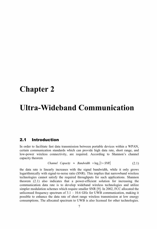
However, as shown in Figure 2.1, due to the low permitted average transmit power of
‒41.25 dBm/MHz, UWB signals stay well below the noise floor of the narrowband
receivers, and hence, will not be distinguishable from noise by the coexisting
narrowband wireless standards. Such spectrum sharing enables a more efficient
utilization of the crowded frequency spectrum [9].
2.2 WiMedia Specifications for UWB
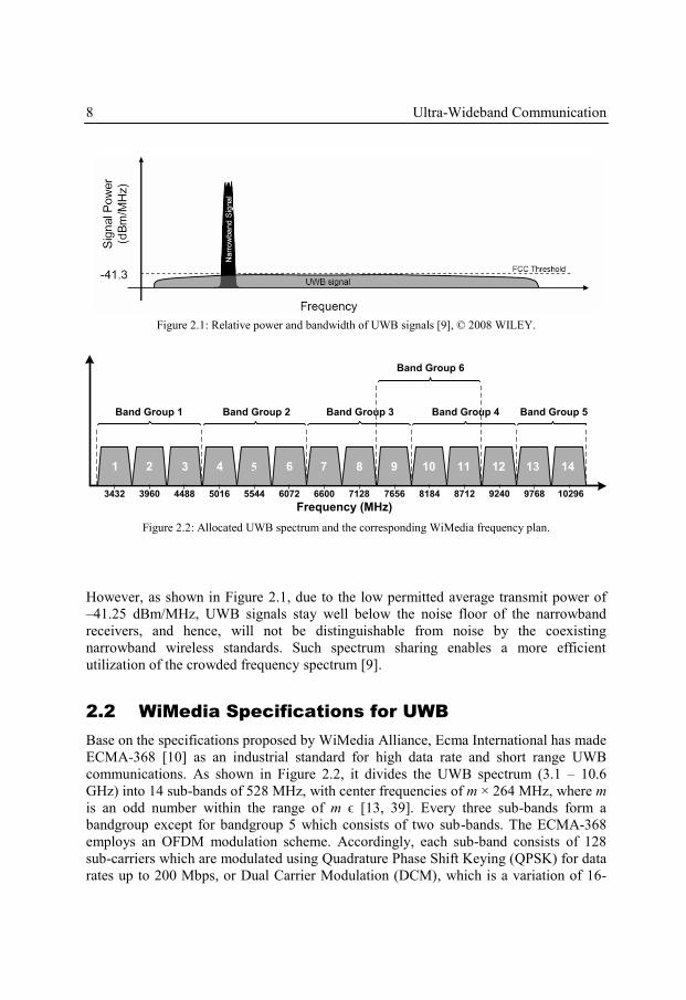
Base on the specifications proposed by WiMedia Alliance, Ecma International has made
ECMA-368 [10] as an industrial standard for high data rate and short range UWB
communications. As shown in Figure 2.2, it divides the UWB spectrum (3.1 ‒ 10.6
GHz) into 14 sub-bands of 528 MHz, with center frequencies of m × 264 MHz, where m
is an odd number within the range of m ϵ [13, 39]. Every three sub-bands form a
bandgroup except for bandgroup 5 which consists of two sub-bands. The ECMA-368
employs an OFDM modulation scheme. Accordingly, each sub-band consists of 128
sub-carriers which are modulated using Quadrature Phase Shift Keying (QPSK) for data
rates up to 200 Mbps, or Dual Carrier Modulation (DCM), which is a variation of 16-
Figure 2.1: Relative power and bandwidth of UWB signals [9], © 2008 WILEY.
Frequency (MHz)
1 2 3 4 5 6 7 8 9 10 11 12 13 14
3432 3960 4488 5016 5544 6072 6600 7128 7656 8184 8712 9240 9768 10296
Band Group 1 Band Group 2 Band Group 3 Band Group 4 Band Group 5
Band Group 6
Figure 2.2: Allocated UWB spectrum and the corresponding WiMedia frequency plan.
2.2 WiMedia Specifications for UWB 9
QAM, for higher data rates up to 480 Mbps. Due to the low transmit power
requirement, more sophisticated modulation schemes are not practical [9]. WiMedia
UWB combines OFDM scheme with band hopping characteristic of FHSS systems.
Therefore, the resulting scheme is more immune to multipath fading and interference.
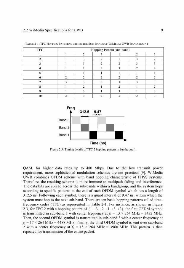
The data bits are spread across the sub-bands within a bandgroup, and the system hops
according to specific patterns at the end of each OFDM symbol which has a length of
312.5 ns. Following each symbol, there is a guard interval of 9.47 ns, within which the
system must hop to the next sub-band. There are ten basic hopping patterns called time-
frequency codes (TFC) as represented in Table 2-1. For instance, as shown in Figure
2.3, for TFC 2 with a hopping pattern of {1→3→2→1→3→2}, the first OFDM symbol
is transmitted in sub-band 1 with center frequency at f1 = 13 × 264 MHz = 3432 MHz.
Then, the second OFDM symbol is transmitted in sub-band 3 with a center frequency at
f3 = 17 × 264 MHz = 4488 MHz. Finally, the third OFDM symbol is sent over sub-band
2 with a center frequency at f2 = 15 × 264 MHz = 3960 MHz. This pattern is then
repeated for transmission of the entire packet.
TABLE 2-1: TFC HOPPING PATTERNS WITHIN THE SUB-BANDS OF WIMEDIA UWB BANDGROUP 1
TFC Hopping Pattern (sub-band)
1 1 2 3 1 2 3
2 1 3 2 1 3 2
3 1 1 2 2 3 3
4 1 1 3 3 2 2
5 1 1 1 1 1 1
6 2 2 2 2 2 2
7 3 3 3 3 3 3
8 1 2 1 2 1 2
9 1 3 1 3 1 3
10 2 3 2 3 2 3
Band 1
Band 2
Band 3
Freq
Time (ns)
9.47312.5
Figure 2.3: Timing details of TFC 2 hopping pattern in bandgroup 1.
10 Ultra-Wideband Communication
2.3 UWB for Wireless USB
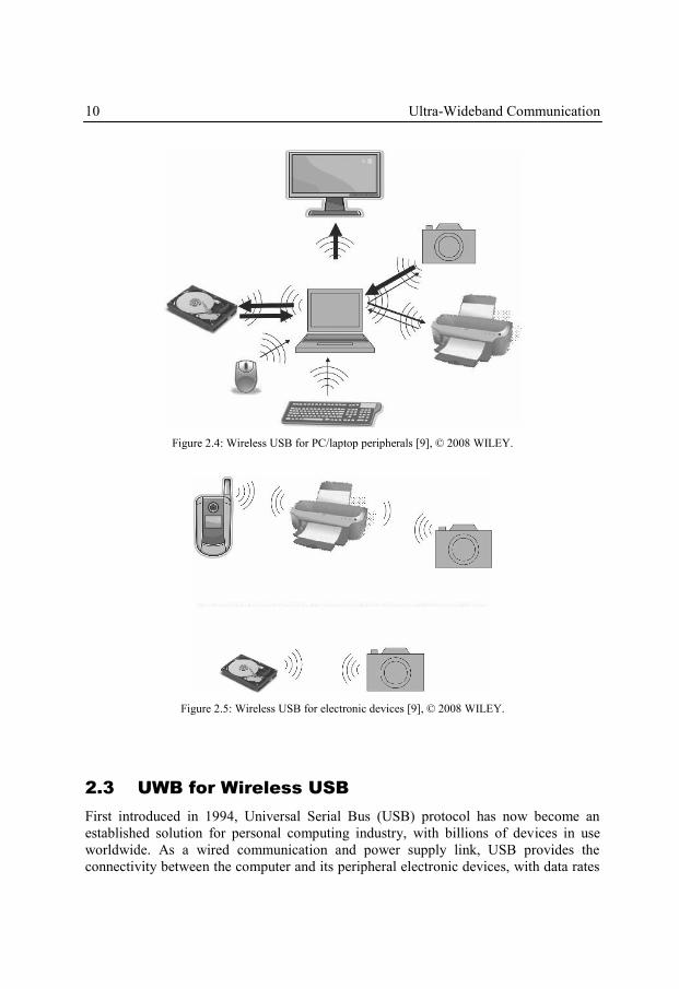
First introduced in 1994, Universal Serial Bus (USB) protocol has now become an
established solution for personal computing industry, with billions of devices in use
worldwide. As a wired communication and power supply link, USB provides the
connectivity between the computer and its peripheral electronic devices, with data rates
Figure 2.4: Wireless USB for PC/laptop peripherals [9], © 2008 WILEY.
Figure 2.5: Wireless USB for electronic devices [9], © 2008 WILEY.
2.4 UWB versus Wi-Fi and 60 GHz Radio 11
up to 480 Mbps, 5 Gbps, and 10 Gbps, for USB 2.0, USB 3.0, and USB 3.1 standards,
respectively. Besides its applications in personal computers and PC peripherals, USB is
nowadays being vastly utilized in mobile phones, PDAs, and digital cameras. However,
the increasing number of USB-enabled devices comes at the cost of too many wired
connections in personal area networks (PAN). In addition, it can lead to running out of
USB ports on PCs and laptops. Furthermore, the limitations on the USB cable length is
disadvantageous from customers’ perspective. One of the main target applications of
WiMedia UWB has been to provide Wireless USB solutions to eliminate the USB
cables, while achieving comparable reliability and data rates with those of wired USB.
Figure 2.4 and Figure 2.5 [9] illustrate basic applications of Wireless USB, through
which the peripheral devices are connected to the PC or laptop, or acting as hosts to
each other.
2.4 UWB versus Wi-Fi and 60 GHz Radio
Recent developments in other wireless technologies such as Wi-Fi and 60 GHz radio
have also made them attractive solutions for high data rate wireless communication,
including Wireless USB. In September 2013, USB Implementers Forum (USB-IF), the
responsible institution for maintaining USB specifications, announced the development
of Media Agnostic USB (MA USB) which is designed to enable the operation of the
USB protocol over several platforms. Accordingly, MA USB will be supporting
WiMedia UWB 3.1 ‒ 10.6 GHz (ECMA-368), WiGig 60 GHz (IEEE 802.11ad), Wi-Fi
2.4 GHz (IEEE 802.11n), and Wi-Fi 5 GHz (IEEE 802.11ac) protocols.
The main goal of UWB is to provide high data rates and short range communication
links with very low energy consumption per transmitted bit. Hence, the battery life time
which is the bottle neck in nowadays portable devices can be saved significantly. This
implies than for portable electronic devices with large data storage, UWB radio link is
beneficial for high speed, short distance and power-efficient transmission of the bulky
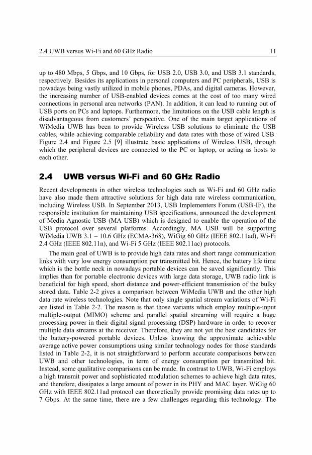
stored data. Table 2-2 gives a comparison between WiMedia UWB and the other high
data rate wireless technologies. Note that only single spatial stream variations of Wi-Fi
are listed in Table 2-2. The reason is that those variants which employ multiple-input
multiple-output (MIMO) scheme and parallel spatial streaming will require a huge
processing power in their digital signal processing (DSP) hardware in order to recover
multiple data streams at the receiver. Therefore, they are not yet the best candidates for
the battery-powered portable devices. Unless knowing the approximate achievable
average active power consumptions using similar technology nodes for those standards
listed in Table 2-2, it is not straightforward to perform accurate comparisons between
UWB and other technologies, in term of energy consumption per transmitted bit.
Instead, some qualitative comparisons can be made. In contrast to UWB, Wi-Fi employs
a high transmit power and sophisticated modulation schemes to achieve high data rates,
and therefore, dissipates a large amount of power in its PHY and MAC layer. WiGig 60
GHz with IEEE 802.11ad protocol can theoretically provide promising data rates up to
7 Gbps. At the same time, there are a few challenges regarding this technology. The
12 Ultra-Wideband Communication
oxygen absorbs 60 GHz millimeter waves, weakening the transmitted signal and
limiting the distance range of WiGig 60 GHz radio links as short as that of WiMedia
UWB. In addition, 60 GHz waves cannot penetrate intervening objects, and hence, an
open line-of-sight communication is required.
Note that the discussion regarding Wi-Fi and 60 GHz radio are only mentioned in
this chapter in order to provide a brief overview of alternative solutions for high data
rate communication. A more detailed comparative discussion requires a thorough study
which falls out of the scope of this thesis.
TABLE 2-2: COMPARISON OF HIGH DATA RATE WIRELESS TECHNOLOGIES
Standard
SIG Max.
data rate
Max.
range
Frequency
band
Max. RF
bandwidth
Modulation
scheme
802.11n † Wi-Fi 150 Mbps 90 m 2.4 GHz/5 GHz 40 MHz 64-QAM
802.11ac † Wi-Fi 433 Mbps 90 m 5 GHz 80 MHz 256-QAM
802.11ac † Wi-Fi 867 Mbps 90 m 5 GHz 160 MHz 256-QAM
802.11ad ‡ WiGig 7 Gbps 10 m 57 ‒ 66 GHz 9 GHz OFDM ǂ
(64-QAM)
ECMA-368 WiMedia 480 Mbps 10 m 3.1 ‒ 10.6 GHz 1.5 GHz MB-OFDM
(QPSK, DCM)
† Single-stream (no MIMO)
‡ Open line-of-sight
ǂ At maximum data rate
13
Chapter 3
Frequency Synthesis for UWB
3.1 Introduction
This chapter presents the requirements on the design of frequency synthesizers for
WiMedia UWB. It also overviews different frequency synthesis techniques and
investigates their potential in satisfying the requirements of UWB communication.
3.2 Synthesizer Requirements
3.2.1 Band Hopping Speed
As mentioned in Chapter 2, WiMedia UWB employs frequency hopping to transmit
OFDM symbols across the sub-bands within a bandgroup. The band hopping period is
equal to the symbol-length of 312.5 ns, plus a guard interval of 9.47 ns, as shown in
Figure 2.3. This implies that the frequency synthesizer must provide a band hopping
speed of less than 9.47 ns. Such a short time slot must in fact include performing a
frequency shift as well as settling to the new center frequency. Compared to other
wireless standards which utilize frequency hopping scheme (such as Bluetooth with a
14 Frequency Synthesis for UWB
band hopping requirement of 200 µs), WiMedia UWB puts a stringent requirement on
frequency synthesizer architectures and circuitries.
3.2.2 Sideband Spurs
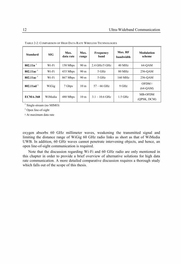
The second challenging requirement in the design of UWB frequency synthesizers is on
the magnitude of the harmonic tones at the output spectrum of the synthesizer. The
coexisting narrowband wireless standards in the UWB spectrum act as strong interferers
to the UWB signals. As shown in Figure 3.1, the main interferers to WiMedia
bandgroup 1 are from IEEE 802.11a/b/g and Bluetooth. The spurious tones at
synthesizer’s output spectrum tend to downconvert the out-of-band interferers into the
signal band and corrupt the wanted signal. To avoid this, the spur-to-carrier ratio (SCR)
must remain below a certain limit. The requirements on synthesizer’s SCR, which can
be calculated from the interferer scenario as presented in [11], imply that all the
spurious tones in the 5 GHz range of IEEE 802.11a (WLAN) need to be below ‒50 dBc.
Similarly, all the spurious tones in the 2.4 GHz ISM band of IEEE 802.11b/g as well as
Bluetooth must be lower than ‒45 dBc. In addition, the interferer scenario also indicates
that all the in-band spurious tones should have a power less than ‒35 dBc [11].
3.2.3 Phase Noise
So as to achieve a less than 0.1 dB SNR deterioration caused by inter-carrier
modulation, the total DC-to-50 MHz integrated phase noise of the synthesized carrier
must be below 2° rms which is equivalent to a phase noise of ‒100 dBc/Hz at an offset
frequency of 1 MHz from the carrier [11]. Therefore, the phase noise requirements are
not as stringent as those of the hopping time and sideband spurs.
3.2.4 In-Phase and Quadrature Mismatch
In order to employ the synthesizer in a zero-IF architecture, both in-phase and
quadrature (IQ) carriers need to be generated by the frequency synthesizer. The
f [MHz]
1 2 3
34
32
39
60
44
88
50
16
55
44
60
72
66
00
71
28
76
56
81
84
87
12
92
40
97
68
10
29
6
BG 1 BG 3 BG 4 BG 5
BG 6
Pin [dB]
24
00
IEEE 802.11a
(WLAN)IEEE 802.11b/g &
Bluetooth
58
00
70dB65dB
BG 2
Figure 3.1: Interference to WiMedia UWB bandgroup 1, from the coexisting wireless technologies.
3.3 Fast Hopping Synthesis Techniques 15
requirements on the IQ mismatch can be obtained by considering the fact that in QPSK
and DCM modulation schemes utilized in OFDM sub-carriers of WiMedia UWB, bit
mapping technique is used which relaxes the IQ mismatch requirements. Consequently
it is sufficient to maintain the IQ mismatch below ‒30 dBc [11].
3.3 Fast Hopping Synthesis Techniques
The stringent requirements on the band hopping speed and spectral purity of the
frequency synthesizer are difficult to be satisfied using conventional approaches. As a
consequence, design of high performance synthesizers for WiMedia UWB application
demands new architectural solutions and circuit techniques. In the following sections,
several synthesizer topologies are investigated and their advantages and drawbacks are
studied.
3.3.1 Single Integer-N PLL
Frequency generation schemes based on PLLs are among the most common and popular
approaches for synthesizing high performance carrier signals for wireless
communication. A PLL is in fact a discrete-time system which is approximated and
modeled as a linear continuous-time system in order to perform stability analysis.
However, this approximation is only valid under a certain condition, that is when the
PLL bandwidth (BW) is less than 10 times its comparison frequency [12] (which is
usually the same as the frequency of the reference clock fref),
10
reffBW . (3.1)
Therefore, there exists an upper bound on PLL’s bandwidth. On the other hand, the
settling time of a feedback system is relative to its loop bandwidth. Therefore, (3.1)
implies that there is also an upper limit on PLL’s settling time. In order to minimize the
settling time, the reference frequency should be increased. However, as the maximum
frequencies provided by standard crystal oscillators are limited, it is not feasible to
achieve fast frequency hopping using PLL-based synthesis approaches. For instance, to
achieve a band hopping speed of ts = 9.47 ns for WiMedia UWB assuming a settling
time of ts = 6τ [13], the required PLL bandwidth is calculated as
2
1BW
MHz1011047.92
69
. (3.2)
In order to provide such a bandwidth while satisfying the stability condition of (3.1), the
reference clock frequency needs to be as large as fref = 1 GHz! Since such a high
16 Frequency Synthesis for UWB
frequency is not realizable with standard crystal oscillators, a synthesizer based on a
single integer-N PLL is not a practical solution for such a fast hopping application.
3.3.2 Fractional-N PLL
In order to resolve the dependency of the loop bandwidth (and so the settling time) on
the input reference frequency, fractional-N PLL-based synthesizers can be employed.
As a consequence, the loop bandwidth of the PLL can be increased to provide a faster
settling [12]. However, the resulting fractional spurs at the output spectrum of such
synthesizers would significantly degrade the spectral purity of the carrier, dissatisfying
the stringent requirements of WiMedia UWB on the spurious performance [11].
3.3.3 Two Integer-N PLLs
Another PLL-based technique to achieve fast frequency hopping for WiMedia UWB is
to utilize two integer-N PLLs in a so called ping-pong configuration [14], [15]. The
operation of the synthesizer is as follows. The first PLL is locked to the center
frequency of the first (current) sub-band, while the second PLL is locked to the center
frequency of the second (next) sub-band. The outputs of the two PLLs are selected by a
high-speed two-to-one multiplexer (MUX). When the hopping command arrives, the
output of the second PLL, which is already settled to the second sub-band, is selected by
the MUX. At the same time, the first PLL switches to the center frequency of the third
sub-band and settles well before the next hopping command arrives. This scheme takes
advantage of two characteristics of WiMedia UWB standard for its operation. First, the
hopping pattern is known to the system, and hence, the center frequencies of the current
and the next sub-bands can be generated accordingly. Second, the OFDM symbol-
length of 312.5 ns will provide enough time margins for each single PLL to settle before
the next hopping edge. A drawback of this technique is that due to the large loop
bandwidth of the PLLs which are required for settling within 312.5 ns, the total
integrated phase noise of 2° rms may not be properly achieved [11].
3.3.4 Three Integer-N PLLs
Assuming a single-bandgroup operation only, the most straightforward PLL-based
scheme for fast hopping frequency synthesis is to simply employ three integer-N PLLs,
each of which locked to the center frequency of one of the sub-bands, and to select the
corresponding carrier frequency using a high speed three-to-one MUX. The advantage
of this approach is that the band hopping time is solely defined by the MUX speed, and
hence, the loop bandwidth of the PLLs can be reduced. As a result, the close-in phase
noise will be sufficiently filtered and the total integrated phase noise of the synthesizer
is minimized. However, there are two drawbacks regarding this technique if LC
oscillators are employed to design the three voltage-controlled oscillators (VCO) [11].
In this case, both the increased silicon area and the injection pulling are unfavorable.
3.3 Fast Hopping Synthesis Techniques 17
Realizing VCOs with ring oscillators [16]‒[18] can alleviate those issues, provided that
the phase noise requirement of ‒100 dBc/Hz can be met.
3.3.5 PLLs and Single-Sideband Mixers
Considering that each bandgroup consists of at most three sub-bands, fast band
switching can be achieved by utilizing two fixed-frequency PLLs and single-sideband
(SSB) mixers. The first PLL generates the center frequency of the middle sub-band
while the second one produces the channel-spacing frequency of 528 MHz. The SSB
mixers take the output frequencies of the two PLLs to generate the required center
frequency of the other two sub-bands through upconversion and downconversion
operations [19]‒[23]. The advantage of employing this architecture is that the band
hopping speed is independent of the settling time of the PLLs. However, there is a
major drawback concerning this architecture. The nonlinearity of the SSB mixers
generates spurious tones close to the frequency of the coexisting wireless standard
which downconvert the out-of-band interferers into the desired UWB band and corrupt
the signal, as discussed in Section 3.2.2. This implies that notch filters are required for
out-of-band suppression as explained in [19]. Moreover, the die area will be increased
due the use of inductors in the two VCOs and/or the SSB mixers [11].
Another variation of this architecture only requires one PLL [24], [25] to save the
silicon area compared to the previous two-PLL case. This comes at the cost of running
the PLL at much higher frequencies and utilizing high-speed frequency dividers which
leads to large power dissipation. Furthermore, designing quadrature frequency dividers
with 50% duty cycle is a challenging task. Also, additional filtering is required to
sufficiently suppress the out-of-band spurs [11].
3.3.6 Sub-Harmonic Injection Locking
Another approach for fast hopping frequency synthesis is based on the concept of sub-
harmonic injection locking [13], [26], [27]. In injection locking technique, an injection
signal is applied to a free running oscillator. If the injection frequency is within the lock
range of the oscillator, the latter stops oscillating at its center frequency to get
synchronized with the externally injected signal. In order to generate a high frequency
carrier signal at the output of an injection-locked oscillator (ILO) from a low frequency
injection signal, the frequency of the latter should be a sub-harmonic of the required
output frequency. For instance, in order to generate the three center frequencies of
WiMedia UWB bandgroup 1 located at f1 = 13 × 264 MHz, f2 = 15 × 264 MHz, and f3 =
17 × 264 MHz, a 264-MHz square wave injection signal is applied to pull the ILO to f1,
f2, and f3, which are the 13th
, 15th
, and 17th
harmonics of the injection signal,
respectively. However, the rich harmonic contents of the square wave injection signal
lead to the pulling of the oscillator by the other strong nearby harmonics. Furthermore,
the harmonic contents of the injection signal will directly appear at the output spectrum
of the synthesizer, degrading the spurious performance. To solve this serious issue, the
wanted harmonic of the input clock should be magnified while all other harmonics are
18 Frequency Synthesis for UWB
sufficiently suppressed. As a consequence, certain pulse shaping techniques should be
developed and applied to the injection signal. Also, additional filtering is necessary to
further suppress the magnitude of the undesired harmonics.
3.3.7 Direct Digital Synthesis
Due to its feedforward operation, direct digital synthesis (DDS) is an attractive
architecture for fast frequency generation. It also provides much less phase noise
compared to a PLL-based approach [28]. However, it is challenging to generate multi-
gigahertz frequencies using DDS due to the following reasons. First, in order to relax
the filtering requirements of the DAC output, the digital circuitries in a DDS need to
operate at about three to four times the output frequency of the DDS [28]. This implies
that for the first bandgroup of WiMedia UWB with a maximum carrier frequency at
4488 MHz, the digital circuitry must operate at a frequency of more than 15 GHz,
which is difficult to achieve. Even if such a high speed can be achieved in future with
more advanced VLSI technologies, the DAC remains the speed bottleneck [28]. One
solution to this problem is to use a fixed high frequency clock from a PLL, and utilize
SSB mixers to add or subtract the lower frequency clock generated by the DDS [29]. In
this architecture, the sinusoidal low frequency IQ signals are stored in a read-only
memory (ROM) look-up table. The high frequency signal of the PLL is also used as the
clock for the ROM and the current steering DACs. An advantage of using DDS for low
frequency signal generation over the presented approach in Section 3.3.5, is that the
harmonic contents of the signal generated by DDS are much lower [11], and hence, the
achieved spurious performance is improved.
3.3.8 DLL-Based Synthesis
DLL-based multipliers consist of two main architectures. Recirculating (or multiplying)
DLLs are in fact similar to ring VCO-based PLLs. The difference is that in a
recirculating DLL, the accumulated jitter within the delay chain is periodically reset
back to zero to achieve a low phase noise characteristic. This is accomplished by using
a MUX to periodically break the feedback loop and inject a clean reference input clock
to the system. In the other architecture which is known as edge-combining DLL, the
multiphase outputs of the DLL are combined using an EC to achieve frequency
multiplication.
The rest of the thesis concentrates on the analysis and design of edge-combining
DLL-based frequency synthesizers for UWB communication and addresses the
opportunities and challenges involved in the design of such systems. Chapter 4 studies
the properties of the DLLs and the edge-combining DLL-based synthesizers in more
details.
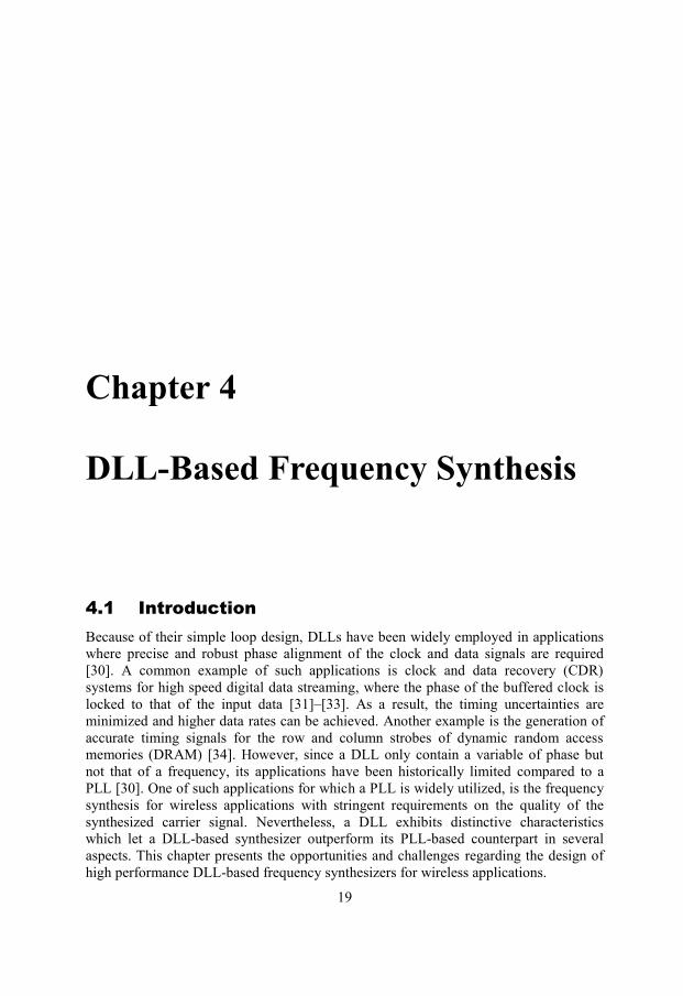
19
Chapter 4
DLL-Based Frequency Synthesis
4.1 Introduction
Because of their simple loop design, DLLs have been widely employed in applications
where precise and robust phase alignment of the clock and data signals are required
[30]. A common example of such applications is clock and data recovery (CDR)
systems for high speed digital data streaming, where the phase of the buffered clock is
locked to that of the input data [31]‒[33]. As a result, the timing uncertainties are
minimized and higher data rates can be achieved. Another example is the generation of
accurate timing signals for the row and column strobes of dynamic random access
memories (DRAM) [34]. However, since a DLL only contain a variable of phase but
not that of a frequency, its applications have been historically limited compared to a
PLL [30]. One of such applications for which a PLL is widely utilized, is the frequency
synthesis for wireless applications with stringent requirements on the quality of the
synthesized carrier signal. Nevertheless, a DLL exhibits distinctive characteristics
which let a DLL-based synthesizer outperform its PLL-based counterpart in several
aspects. This chapter presents the opportunities and challenges regarding the design of
high performance DLL-based frequency synthesizers for wireless applications.
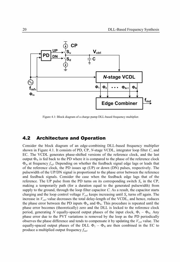
20 DLL-Based Frequency Synthesis
4.2 Architecture and Operation
Consider the block diagram of an edge-combining DLL-based frequency multiplier
shown in Figure 4.1. It consists of PD, CP, N-stage VCDL, integrator loop filter C, and
EC. The VCDL generates phase-shifted versions of the reference clock, and the last
output ФN is fed back to the PD where it is compared to the phase of the reference clock
Фin at frequency fref. Depending on whether the feedback signal edge lags or leads that
of the reference clock, the PD issues up (UP) or down (DN) pulses, respectively. The
pulsewidth of the UP/DN signal is proportional to the phase error between the reference
and feedback signals. Consider the case when the feedback edge lags that of the
reference. The UP pulse from the PD turns on its corresponding switch Su in the CP,
making a temporarily path (for a duration equal to the generated pulsewidth) from
supply to the ground, through the loop filter capacitor C. As a result, the capacitor starts
charging and the loop control voltage Vctrl keeps increasing until Su turns off again. The
increase in Vctrl value decreases the total delay-length of the VCDL, and hence, reduces
the phase error between the PD inputs Фin and ФN. This procedure is repeated until the
phase error becomes (theoretically) zero and the DLL is locked to the reference clock
period, generating N equally-spaced output phases of the input clock, Ф1 ‒ ФN. Any
phase error due to the PVT variations is removed by the loop as the PD periodically
observes the phase difference and tends to compensate it by updating the Vctrl value. The
equally-spaced output phases of the DLL Ф1 ‒ ФN are then combined in the EC to
produce a multiplied output frequency fout.
PD
Edge Combiner
UP
DN
fout
N-stage VCDL
···
Vctrl
fref,Φin
C
CP
Su
Sd
Φ1 ΦN ΦN-1 Φ2
Figure 4.1: Block diagram of a charge pump DLL-based frequency multiplier.
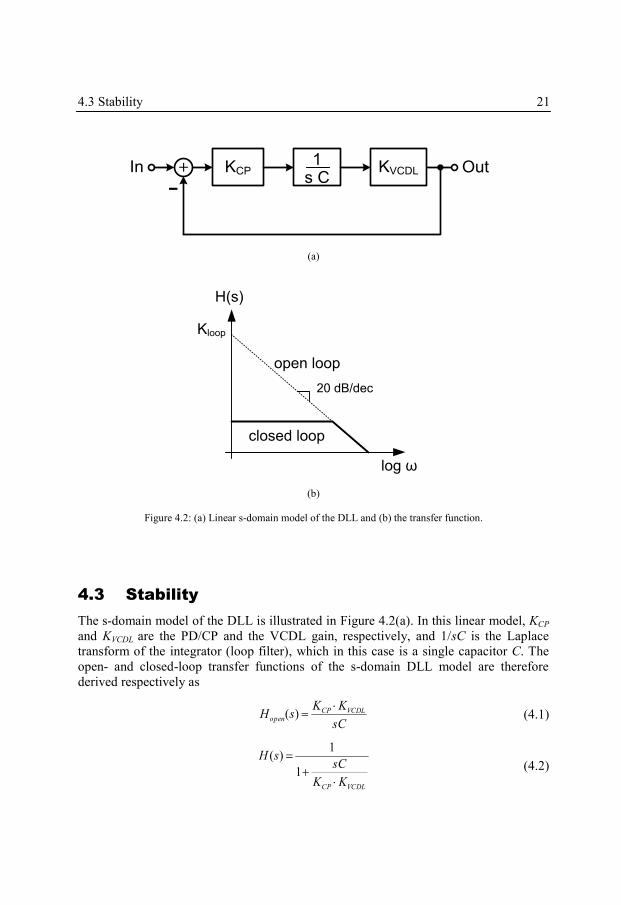
4.3 Stability 21
4.3 Stability
The s-domain model of the DLL is illustrated in Figure 4.2(a). In this linear model, KCP
and KVCDL are the PD/CP and the VCDL gain, respectively, and 1/sC is the Laplace
transform of the integrator (loop filter), which in this case is a single capacitor C. The
open- and closed-loop transfer functions of the s-domain DLL model are therefore
derived respectively as
sC
KKsH VCDLCP
open
)( (4.1)
VCDLCP KK
sCsH
1
1)(
(4.2)
KCP KVCDL OutIn +1
s C−
(a)
H(s)
log ω
open loop
closed loop
Kloop
20 dB/dec
(b)
Figure 4.2: (a) Linear s-domain model of the DLL and (b) the transfer function.
22 DLL-Based Frequency Synthesis
Figure 4.2(b) compares the open- and closed-loop s-domain transfer functions of the
DLL by plotting (4.1) and (4.2). Since the DLL only contains a variable of phase, only
one integrator within the loop can eliminate the finite gain at DC [30], and hence,
remove the static phase error of the loop. This has been resulted in a first-order transfer
function of (4.2). Containing only one integrator, the open-loop phase margin of the
DLL is 90°, and therefore, the loop is unconditionally stable provided that the phase
margin is not significantly deteriorated by the delay in the loop, and also that the loop
bandwidth is not very close to the reference frequency. Also, the low-pass characteristic
of the DLL transfer function in (4.2) implies that for those input signals whose
frequencies are within the loop bandwidth of the DLL, the phase of the output signal
tracks that of the input. On the other hand, the loop exhibits a high-pass characteristic
for an injected noise to the output node. Therefore, any noise at the output which is
within the DLL loop bandwidth will be filtered out.
In a PLL, on the other hand, (at least) two integrators are required to eliminate the
gain at DC, as it has both variables of phase and frequency. Therefore, a PLL is (at
least) a second-order system with stability issues which should be carefully considered
during the design procedure. As a consequence, the design of a PLL-based system will
be more complicated and requires more effort than its DLL-based counterpart.
4.4 Loop Bandwidth and Settling Time
As DLL is a first order system, its loop bandwidth can be chosen relatively wide while
still remaining stable. This implies that the settling time can be improved as it is
inversely proportional to the loop bandwidth. However, if a large bandwidth is utilized,
the s-domain linear model will not be valid anymore. This is due to the fact that a CP
DLL is a discrete-time system which can be approximated as a continuous-time system
provided that its bandwidth is sufficiently smaller than the comparison frequency.
Otherwise, a more accurate model which analyzes the time-domain response should be
employed. A discrete-time z-domain model of the DLL is shown in Figure 4.3. For this
model the open-loop gain K and the transfer function are expressed respectively as
+ KCP KVCDL
1
C (1 z-1
)
z-1
_tin tout
−
Figure 4.3: z-domain model for a wideband DLL.
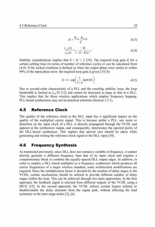
4.5 Reference Clock 23
C
KKK VCDLCP (4.3)
1)1(1)(
)(
zK
K
zt
zt
in
out . (4.4)
Stability considerations implies that 0 < K < 2 [35]. The required loop gain K for a
certain settling time (in terms of number of reference cycles n) can be calculated from
(4.4). If the locked condition is defined as when the output phase error settles to within
99% of the input phase error, the required loop gain is given [35] by
)01.0ln(
1
1exp1
nK . (4.5)
Due to second-order characteristic of a PLL and the resulting stability issue, the loop
bandwidth is limited to fref/10 [12] and cannot be increased as large as that in a DLL.
This implies that for those wireless applications which employ frequency hopping,
PLL-based synthesizers may not be practical solutions (Section 3.3.1).
4.5 Reference Clock
The quality of the reference clock to the DLL input has a significant impact on the
quality of the multiplied carrier signal. This is because unlike a PLL, any noise or
distortion on the input clock of a DLL is directly propagated through the VCDL and
appears at the synthesizer output, and consequently, deteriorates the spectral purity of
the DLL-based synthesizer. This implies that special care should be taken while
generating and routing the reference clock signal to the DLL input [30].
4.6 Frequency Synthesis
As mentioned previously, since DLL does not contain a variable of frequency, it cannot
directly generate a different frequency than that of its input clock and requires a
complementary block to combine the equally-spaced DLL output edges. In addition, in
order to employ a DLL-based multiplier as a frequency synthesizer which produces all
carrier frequencies of a target wireless standard, some architectural modifications are
required. Since the multiplication factor is decided by the number of delay stages in the
VCDL, certain mechanisms should be utilized to provide different number of delay
stages within the loop. This can be achieved through two main approaches. In the first
approach, the feedback signal is selected from different outputs of the VCDL using a
MUX [35]. In the second approach, the VCDL utilizes certain bypass scheme to
disable/enable the delay elements from the signal path, without affecting the load
symmetry at the inter-stage nodes [3], [6].
24 DLL-Based Frequency Synthesis
4.7 Random Jitter and Phase Noise
The spectral power of an ideal carrier signal is concentrated on its center frequency.
However in practice, due to the effect of noise which results in random clock jitter, the
carrier spectrum exhibits a skirt around the center frequency, causing phase noise in the
synthesized signal. The phase noise characteristic of the frequency synthesizer will
significantly affect the performance of radio front-ends, both in receiver (SNR) and
transmitter (EVM) sides. As can be observed from Figure 4.4(a), in a PLL-based clock
multiplier which is based on a ring VCO, the random jitter within the delay line is
accumulated over several reference cycles. This is due to the feedback connection from
the output to the input of the delay chain. The number of accumulation cycles is
determined by the response time of the PLL which is limited to its bandwidth due to the
stability concerns [36], as discussed in Section 4.4. As a consequence, such architecture
exhibits a relatively poor phase noise profile. In a DLL-based frequency multiplier, on
the other hand, the noise-induced timing jitter in the delay line which is accumulated
within a single reference cycle is periodically reset back to zero at each comparison
instant of the phase detector. This phenomenon which can be observed from Figure
4.4(b), implies that a DLL-based frequency multiplier exhibits a flat phase noise profile
for offset frequencies less than fref [35], [36].
4.8 Periodic Jitter and Harmonic Spurs
Besides the noise-induced random jitter which degrades the phase noise performance of
the synthesized carrier signal, there is another error source which degrades the spectral
purity of a DLL-based frequency synthesizer, known as periodic jitter. In contrast to the
random jitter, the periodic jitter exhibits a fixed-pattern characteristic and results in an
erroneous periodicity which repeats itself at every cycle of the reference clock. In
frequency domain, the effect of such imperfection translates itself to the harmonic tones
located at integer multiples of the reference clock. These harmonic tones which are also
known as harmonic spurs, sideband spurs or spurious tones will downconvert the
potential out-of-band interferers into the desired channel and corrupt the wanted signal.
There are several sources which are responsible for generation of harmonic spurs in
locked-loop-based synthesizers. In analog phase-locked systems, such as a VCO-based
PLL, and a VCDL-based DLL, any periodic disturbance on the loop control voltage
results in sidebands spurs. The voltage ripple in fact occurs by the PD and CP
imperfections [37]. The ripple’s magnitude and thus the resulting harmonic spurs can be
minimized to some extent, by utilizing a larger loop filter capacitor [28]. However, in
case of edge-combining DLL-based synthesizer, there are additional sources of periodic
jitter that significantly deteriorate the overall spurious performance. Since the
generation of multiplied output is performed by combining the equally-spaced
multiphase output edges of the DLL, any misalignment of those edges will result in
periodic jitter.
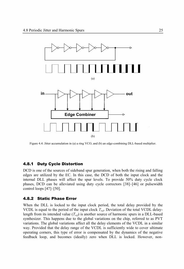
4.8 Periodic Jitter and Harmonic Spurs 25
4.8.1 Duty Cycle Distortion
DCD is one of the sources of sideband spur generation, when both the rising and falling
edges are utilized by the EC. In this case, the DCD of both the input clock and the
internal DLL phases will affect the spur levels. To provide 50% duty cycle clock
phases, DCD can be alleviated using duty cycle correctors [38]‒[46] or pulsewidth
control loops [47]‒[50].
4.8.2 Static Phase Error
When the DLL is locked to the input clock period, the total delay provided by the
VCDL is equal to the period of the input clock Tref. Deviation of the total VCDL delay-
length from its intended value (Tref) is another source of harmonic spurs in a DLL-based
synthesizer. This happens due to the global variations on the chip, referred to as PVT
variations. The global variations affect all the delay elements of the VCDL in a similar
way. Provided that the delay range of the VCDL is sufficiently wide to cover ultimate
operating corners, this type of error is compensated by the dynamics of the negative
feedback loop, and becomes (ideally) zero when DLL is locked. However, non-
(a)
(b)
Figure 4.4: Jitter accumulation in (a) a ring VCO, and (b) an edge-combining DLL-based multiplier.
26 DLL-Based Frequency Synthesis
idealities such as the mismatch between the UP/DN signals in PD and CP respectively,
leaves a small timing offset between the reference and the feedback signals, even when
the loop is locked. In order to minimize SPE and its contribution to the magnitude of the
spurious tones at the output of a the synthesizer, certain calibration algorithms and
circuit techniques should be employed [51]‒[54].
4.8.3 Delay Mismatch
The local manufacturing imperfections are the other source of spur generation in DLL-
based synthesizers. Such local variations result in delay mismatch among the identically
designed delay stages of the delay line. The delay mismatch is a stochastic variable and
causes such a delay deviation which is regional to each delay stage, and therefore,
cannot be eliminated by the loop.
The spurious performance of DLL-based synthesizers has not been thoroughly
investigated in the literatures. A comprehensive mathematical analysis of the reference
harmonic spurs in such synthesizers has been studied and covered in Chapters 5 ‒ 7.
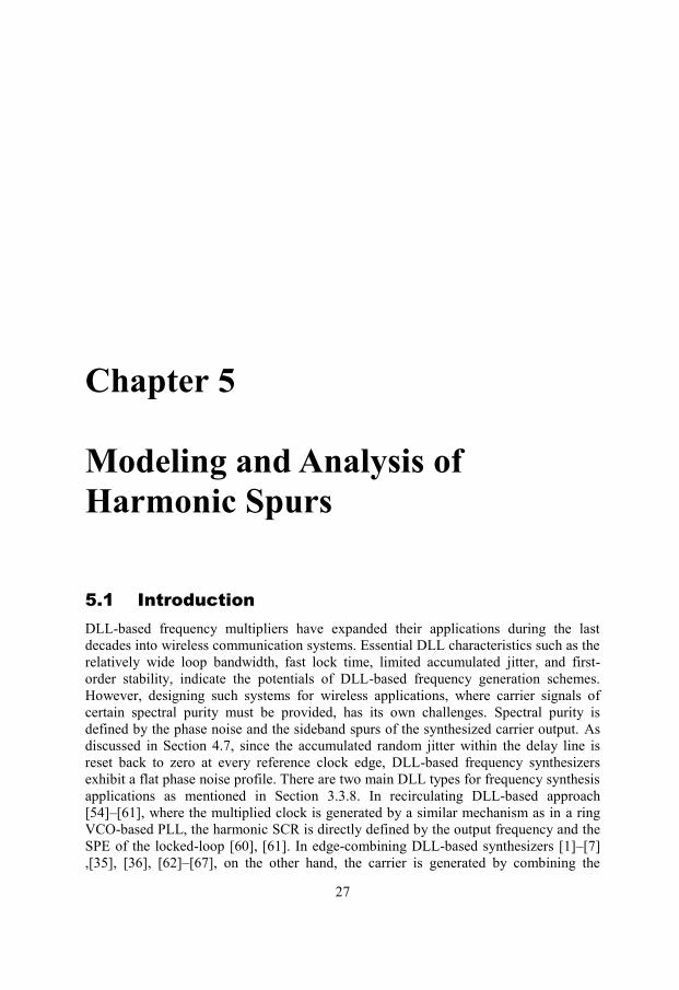
27
Chapter 5
Modeling and Analysis of
Harmonic Spurs
5.1 Introduction
DLL-based frequency multipliers have expanded their applications during the last
decades into wireless communication systems. Essential DLL characteristics such as the
relatively wide loop bandwidth, fast lock time, limited accumulated jitter, and first-
order stability, indicate the potentials of DLL-based frequency generation schemes.
However, designing such systems for wireless applications, where carrier signals of
certain spectral purity must be provided, has its own challenges. Spectral purity is
defined by the phase noise and the sideband spurs of the synthesized carrier output. As
discussed in Section 4.7, since the accumulated random jitter within the delay line is
reset back to zero at every reference clock edge, DLL-based frequency synthesizers
exhibit a flat phase noise profile. There are two main DLL types for frequency synthesis
applications as mentioned in Section 3.3.8. In recirculating DLL-based approach
[54]‒[61], where the multiplied clock is generated by a similar mechanism as in a ring
VCO-based PLL, the harmonic SCR is directly defined by the output frequency and the
SPE of the locked-loop [60], [61]. In edge-combining DLL-based synthesizers [1]‒[7]
,[35], [36], [62]‒[67], on the other hand, the carrier is generated by combining the
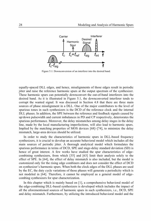
28 Modeling and Analysis of Harmonic Spurs
equally-spaced DLL edges, and hence, misalignments of those edges result in periodic
jitter and raise the reference harmonic spurs at the output spectrum of the synthesizer.
These harmonic spurs can potentially downconvert the out-of-band interferers into the
desired band. As it is illustrated in Figure 5.1, the downconverted interferer tends to
corrupt the wanted signal. It was discussed in Section 4.8 that there are three main
sources of phase misalignment in a DLL. One of the major contributors to the level of
spurious tones in such synthesizers is the DCD of the reference clock and the internal
DLL phases. In addition, the SPE between the reference and feedback signals caused by
up/down pulsewidth and current imbalances in PD and CP respectively, deteriorates the
spurious performance. Moreover, the delay mismatches among delay stages in the delay
line, made by the local manufacturing imperfections, will also lead to harmonic spurs.
Implied by the matching properties of MOS devices [68]‒[74], to minimize the delay
mismatch, large-area devices should be utilized.
In order to study the characteristics of harmonic spurs in DLL-based frequency
synthesizers, it is crucial to develop an accurate behavioral model which includes all the
main sources of periodic jitter. A thorough analytical model which formulates the
spurious performance in terms of DCD, SPE and stage-delay standard deviation (SD) is
hence of great interest. A few works have studied the spur characteristics of edge-
combining synthesizers, from which [35] and [63] limit their analysis solely to the
effect of SPE. In [64], the effect of delay mismatch is also included, but the model is
customized only for the rising edge combiners and does not consider the effect of DCD
on synthesizer’s harmonic spurs. When both the clock edges of the DLL phases are used
by the EC, the duty cycle variations of those phases will generate a periodicity which is
not modeled in [64]. Therefore, it cannot be employed as a general model of edge-
combing synthesizers for spur characterization.
In this chapter which is mainly based on [1], a comprehensive behavioral model of
the edge-combining DLL-based synthesizers is developed which includes the impact of
all the aforementioned sources of harmonic spurs in such synthesizers, i.e., DCD, SPE
and delay mismatch. Furthermore, by utilizing the introduced behavioral model and the
f fintfsigfc+freffc
InterfererDesired
SignalHarmonic
Spur
Carrier
f fc-fsig
Figure 5.1: Downconversion of an interferer into the desired band.
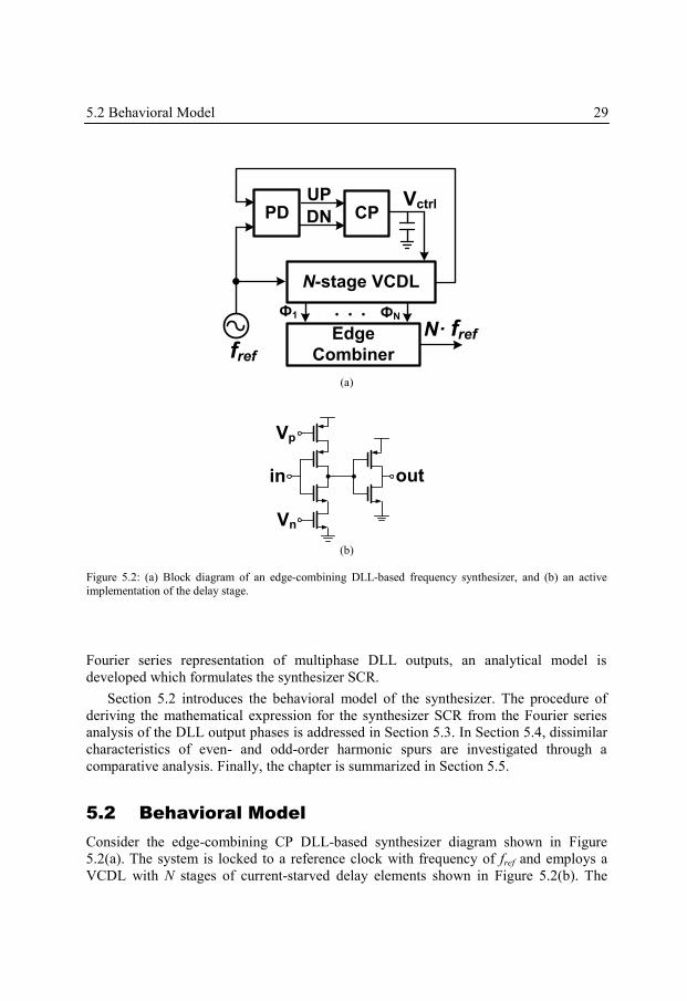
5.2 Behavioral Model 29
Fourier series representation of multiphase DLL outputs, an analytical model is
developed which formulates the synthesizer SCR.
Section 5.2 introduces the behavioral model of the synthesizer. The procedure of
deriving the mathematical expression for the synthesizer SCR from the Fourier series
analysis of the DLL output phases is addressed in Section 5.3. In Section 5.4, dissimilar
characteristics of even- and odd-order harmonic spurs are investigated through a
comparative analysis. Finally, the chapter is summarized in Section 5.5.
5.2 Behavioral Model
Consider the edge-combining CP DLL-based synthesizer diagram shown in Figure
5.2(a). The system is locked to a reference clock with frequency of fref and employs a
VCDL with N stages of current-starved delay elements shown in Figure 5.2(b). The
PD
Edge
Combiner
UP
DN
N· fref
N-stage VCDL
· · ·
VctrlCP
fref
Ф1 ФN
(a)
Vp
in out
Vn
(b)
Figure 5.2: (a) Block diagram of an edge-combining DLL-based frequency synthesizer, and (b) an active
implementation of the delay stage.
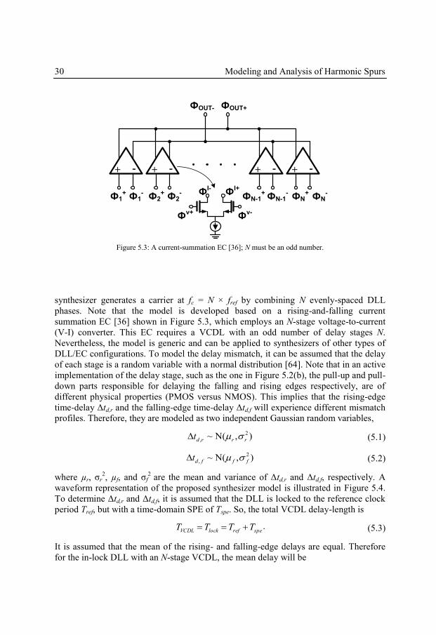
30 Modeling and Analysis of Harmonic Spurs
synthesizer generates a carrier at fc = N × fref by combining N evenly-spaced DLL
phases. Note that the model is developed based on a rising-and-falling current
summation EC [36] shown in Figure 5.3, which employs an N-stage voltage-to-current
(V-I) converter. This EC requires a VCDL with an odd number of delay stages N.
Nevertheless, the model is generic and can be applied to synthesizers of other types of
DLL/EC configurations. To model the delay mismatch, it can be assumed that the delay
of each stage is a random variable with a normal distribution [64]. Note that in an active
implementation of the delay stage, such as the one in Figure 5.2(b), the pull-up and pull-
down parts responsible for delaying the falling and rising edges respectively, are of
different physical properties (PMOS versus NMOS). This implies that the rising-edge
time-delay Δtd,r and the falling-edge time-delay Δtd,f will experience different mismatch
profiles. Therefore, they are modeled as two independent Gaussian random variables,
),(~ 2
, rrrdt (5.1)
),(~ 2
, fffdt (5.2)
where µr, σr2, µf, and σf
2 are the mean and variance of Δtd,r and Δtd,f, respectively. A
waveform representation of the proposed synthesizer model is illustrated in Figure 5.4.
To determine Δtd,r and Δtd,f, it is assumed that the DLL is locked to the reference clock
period Tref, but with a time-domain SPE of Tspe. So, the total VCDL delay-length is
spereflockVCDL TTTT . (5.3)
It is assumed that the mean of the rising- and falling-edge delays are equal. Therefore
for the in-lock DLL with an N-stage VCDL, the mean delay will be
+ - + -+ - + -
Ф1+
Ф1-
Ф2+
Ф2-
ФN-1+
ФN-1-
ФN+
ФOUT- ФOUT+
Фv+
Фv-
ФI-
ФI+
ФN-
Figure 5.3: A current-summation EC [36]; N must be an odd number.
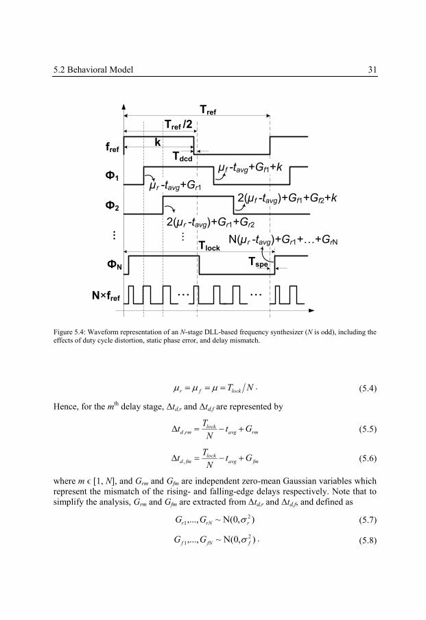
5.2 Behavioral Model 31
NTlockfr . (5.4)
Hence, for the mth
delay stage, Δtd,r and Δtd,f are represented by
rmavglock
rmd GtN
Tt ,
(5.5)
fmavglock
fmd GtN
Tt ,
(5.6)
where m ϵ [1, N], and Grm and Gfm are independent zero-mean Gaussian variables which
represent the mismatch of the rising- and falling-edge delays respectively. Note that to
simplify the analysis, Grm and Gfm are extracted from Δtd,r and Δtd,f, and defined as
),0(~,..., 2
1 rrNr GG (5.7)
),0(~,..., 2
1 ffNf GG . (5.8)
Tref
Tref /2
k
Tdcd
Tspe
fref
Ф2
Ф1
ФN
· · ·
···
Tlock
··· N×fref
2(µr -tavg)+Gr1+Gr2
µr -tavg+Gr1
µf -tavg+Gf1+k
2(µf -tavg)+Gf1+Gf2+k
N(µr -tavg)+Gr1+…+GrN· · ·
Figure 5.4: Waveform representation of an N-stage DLL-based frequency synthesizer (N is odd), including the effects of duty cycle distortion, static phase error, and delay mismatch.
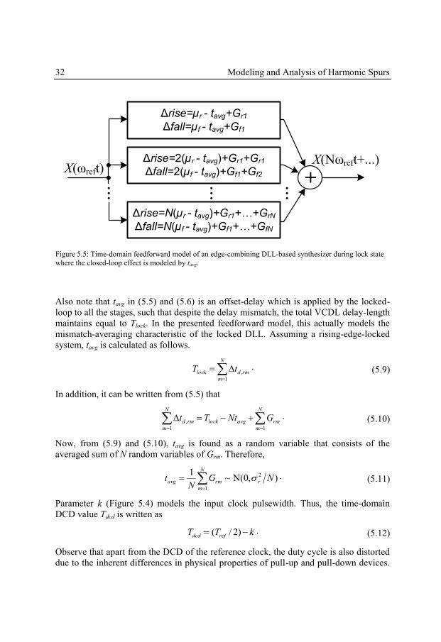
32 Modeling and Analysis of Harmonic Spurs
Also note that tavg in (5.5) and (5.6) is an offset-delay which is applied by the locked-
loop to all the stages, such that despite the delay mismatch, the total VCDL delay-length
maintains equal to Tlock. In the presented feedforward model, this actually models the
mismatch-averaging characteristic of the locked DLL. Assuming a rising-edge-locked
system, tavg is calculated as follows.
N
m
rmdlock tT1
,. (5.9)
In addition, it can be written from (5.5) that
N
m
rmavglock
N
m
rmd GNtTt11
,. (5.10)
Now, from (5.9) and (5.10), tavg is found as a random variable that consists of the
averaged sum of N random variables of Grm. Therefore,
),0(~1 2
1
NGN
t r
N
m
rmavg
. (5.11)
Parameter k (Figure 5.4) models the input clock pulsewidth. Thus, the time-domain
DCD value Tdcd is written as
kTT refdcd )2/( . (5.12)
Observe that apart from the DCD of the reference clock, the duty cycle is also distorted
due to the inherent differences in physical properties of pull-up and pull-down devices.
+
...
...
...
X(ωreft)X(Nωreft+...)
Δrise=µr - tavg+Gr1
Δfall=µf - tavg+Gf1
Δrise=2(µr - tavg)+Gr1+Gr1
Δfall=2(µf - tavg)+Gf1+Gf2
Δrise=N(µr - tavg)+Gr1+…+GrN
Δfall=N(µf - tavg)+Gf1+…+GfN
Figure 5.5: Time-domain feedforward model of an edge-combining DLL-based synthesizer during lock state
where the closed-loop effect is modeled by tavg.
5.3 Analytical Model 33
Utilizing (5.1) and (5.2), and applying the linearity property, it can be shown that the so-
called internal duty cycle distortion (IDCD) within a delay stage follows a normal
distribution which is defined by
22
,, ,~IDCD frfrfdrd tt . (5.13)
Expression (5.13) implies that an accurate ratio-sizing between the pull-up and pull-
down devices, as assumed in (5.4), can only eliminate the mean of IDCD,
demonstrating that the inter-stage DCD is correlated to the delay mismatch.
Figure 5.5 depicts the time-domain diagram of the introduced feedforward model.
The combined output is generated by summation of the time-shifted versions of the
rising and falling reference clock edges (in current domain), and contains a fundamental
tone fc = N × fref, as well as the reference harmonic components. The model is
implemented in MATLAB and the SCR at the synthesizer’s output spectrum is
calculated for each MC sample (of randomized Gr and Gf values), by taking the fast
Fourier transform (FFT) of the output signal. The corresponding results act as a
reference for validity-check of the developed analytical model in the next section.
5.3 Analytical Model
Based on the introduced behavioral model in the previous section, an analytical model
is developed in this section which formulates the synthesizer’s spurious performance in
terms of DCD, SPE and delay SD. Containing the magnitude, phase and frequency
information of periodic signals, Fourier series are efficient tools for analyzing the
square wave multiphase DLL outputs. The Fourier series of the mth
DLL output phase is
expressed as
1
,
1
,,0 )sin()cos()(n
refn
n
refnm tnbtnaatmmm
(5.14)
where
2/
2/
0,0 )(
T
Tm
ref
dttT
Aa
m
(5.15)
2/
2/
0, )cos()(
2 T
Trefm
ref
n dttntT
Aa
m
(5.16)
2/
2/
0, )sin()(
2 T
Trefm
ref
n dttntT
Ab
m . (5.17)
From the waveform representation of the DLL outputs in Figure 5.4, the corresponding
Fourier coefficients an,Φm and bn,Φm in (5.16) and (5.17) are expressed by
34 Modeling and Analysis of Harmonic Spurs
m
i
avgfi
m
i
avgri
m
mtGmk
mtGmref
ref
n dttnT
Aa 1
1
)cos(2 0
,
(5.18)
m
i
avgfi
m
i
avgri
m
mtGmk
mtGmref
ref
n dttnT
Ab 1
1
)sin(2 0
,
. (5.19)
Note that the DC component a0,Φm is excluded for the rest of the analysis for the sake of
simplicity. Since the EC output is constructed by summation of the multiphase DLL
currents, its Fourier series can be written as
N
m
mout tt1
)()(
N
m
N
m n
refn
n
refn tnbtnamm
1 1 1
,
1
, )sin()cos( . (5.20)
From linearity, (5.20) can be rearranged as follows.
1 1
,
1 1
, )sin()cos()(n
N
m
nref
n
N
m
nrefout mmbtnatnt . (5.21)
Concluded from (5.21), the Fourier coefficients of the EC output are the sum of Fourier
coefficients of the DLL phases. So, an Fourier coefficient of the EC output is
N
mmnn aa
1
,
N
m
mtGmk
mtGmref
ref
m
i
avgfi
m
i
avgri
dttnT
A
1
01
1
)cos(2
rmfm
speref
ref
N
m
rmfm
ref
XXkN
TTm
T
nXXk
T
n
n
A )(2cossin
2
1
0
. (5.22)
Similarly, bn Fourier coefficient of the EC output is expressed by
N
mmnn bb
1
,
N
m
mtGmk
mtGmref
ref
m
i
avgfi
m
i
avgri
dttnT
A
1
01
1
)sin(2
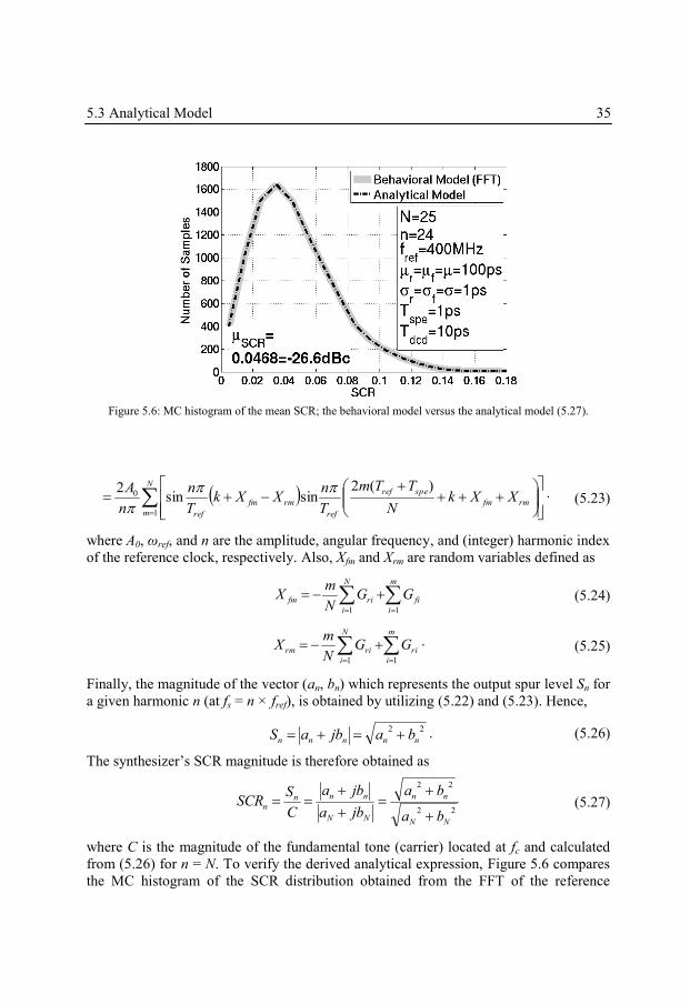
5.3 Analytical Model 35
rmfm
speref
ref
N
m
rmfm
ref
XXkN
TTm
T
nXXk
T
n
n
A )(2sinsin
2
1
0
. (5.23)
where A0, ωref, and n are the amplitude, angular frequency, and (integer) harmonic index
of the reference clock, respectively. Also, Xfm and Xrm are random variables defined as
m
i
fi
N
i
rifm GGN
mX
11
(5.24)
m
i
ri
N
i
rirm GGN
mX
11
. (5.25)
Finally, the magnitude of the vector (an, bn) which represents the output spur level Sn for
a given harmonic n (at fs = n × fref), is obtained by utilizing (5.22) and (5.23). Hence,
22
nnnnn bajbaS . (5.26)
The synthesizer’s SCR magnitude is therefore obtained as
22
22
NN
nn
NN
nnnn
ba
ba
jba
jba
C
SSCR
(5.27)
where C is the magnitude of the fundamental tone (carrier) located at fc and calculated
from (5.26) for n = N. To verify the derived analytical expression, Figure 5.6 compares
the MC histogram of the SCR distribution obtained from the FFT of the reference
Figure 5.6: MC histogram of the mean SCR; the behavioral model versus the analytical model (5.27).
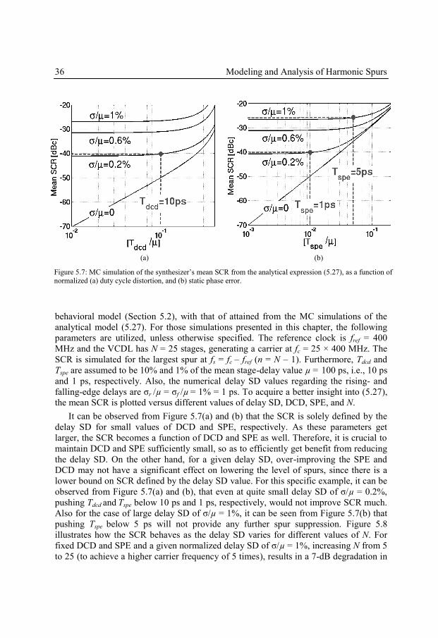
36 Modeling and Analysis of Harmonic Spurs
behavioral model (Section 5.2), with that of attained from the MC simulations of the
analytical model (5.27). For those simulations presented in this chapter, the following
parameters are utilized, unless otherwise specified. The reference clock is fref = 400
MHz and the VCDL has N = 25 stages, generating a carrier at fc = 25 × 400 MHz. The
SCR is simulated for the largest spur at fs = fc – fref (n = N – 1). Furthermore, Tdcd and
Tspe are assumed to be 10% and 1% of the mean stage-delay value µ = 100 ps, i.e., 10 ps
and 1 ps, respectively. Also, the numerical delay SD values regarding the rising- and
falling-edge delays are σr /µ = σf /µ = 1% = 1 ps. To acquire a better insight into (5.27),
the mean SCR is plotted versus different values of delay SD, DCD, SPE, and N.
It can be observed from Figure 5.7(a) and (b) that the SCR is solely defined by the
delay SD for small values of DCD and SPE, respectively. As these parameters get
larger, the SCR becomes a function of DCD and SPE as well. Therefore, it is crucial to
maintain DCD and SPE sufficiently small, so as to efficiently get benefit from reducing
the delay SD. On the other hand, for a given delay SD, over-improving the SPE and
DCD may not have a significant effect on lowering the level of spurs, since there is a
lower bound on SCR defined by the delay SD value. For this specific example, it can be
observed from Figure 5.7(a) and (b), that even at quite small delay SD of σ/µ = 0.2%,
pushing Tdcd and Tspe below 10 ps and 1 ps, respectively, would not improve SCR much.
Also for the case of large delay SD of σ/µ = 1%, it can be seen from Figure 5.7(b) that
pushing Tspe below 5 ps will not provide any further spur suppression. Figure 5.8
illustrates how the SCR behaves as the delay SD varies for different values of N. For
fixed DCD and SPE and a given normalized delay SD of σ/µ = 1%, increasing N from 5
to 25 (to achieve a higher carrier frequency of 5 times), results in a 7-dB degradation in
(a) (b)
Figure 5.7: MC simulation of the synthesizer’s mean SCR from the analytical expression (5.27), as a function of normalized (a) duty cycle distortion, and (b) static phase error.
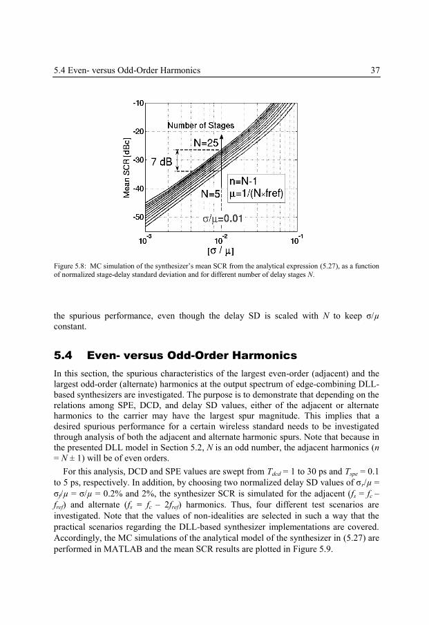
5.4 Even- versus Odd-Order Harmonics 37
the spurious performance, even though the delay SD is scaled with N to keep σ/µ
constant.
5.4 Even- versus Odd-Order Harmonics
In this section, the spurious characteristics of the largest even-order (adjacent) and the
largest odd-order (alternate) harmonics at the output spectrum of edge-combining DLL-
based synthesizers are investigated. The purpose is to demonstrate that depending on the
relations among SPE, DCD, and delay SD values, either of the adjacent or alternate
harmonics to the carrier may have the largest spur magnitude. This implies that a
desired spurious performance for a certain wireless standard needs to be investigated
through analysis of both the adjacent and alternate harmonic spurs. Note that because in
the presented DLL model in Section 5.2, N is an odd number, the adjacent harmonics (n
= N ± 1) will be of even orders.
For this analysis, DCD and SPE values are swept from Tdcd = 1 to 30 ps and Tspe = 0.1
to 5 ps, respectively. In addition, by choosing two normalized delay SD values of σr/µ =
σf/µ = σ/µ = 0.2% and 2%, the synthesizer SCR is simulated for the adjacent (fs = fc ‒
fref) and alternate (fs = fc ‒ 2fref) harmonics. Thus, four different test scenarios are
investigated. Note that the values of non-idealities are selected in such a way that the
practical scenarios regarding the DLL-based synthesizer implementations are covered.
Accordingly, the MC simulations of the analytical model of the synthesizer in (5.27) are
performed in MATLAB and the mean SCR results are plotted in Figure 5.9.
Figure 5.8: MC simulation of the synthesizer’s mean SCR from the analytical expression (5.27), as a function
of normalized stage-delay standard deviation and for different number of delay stages N.
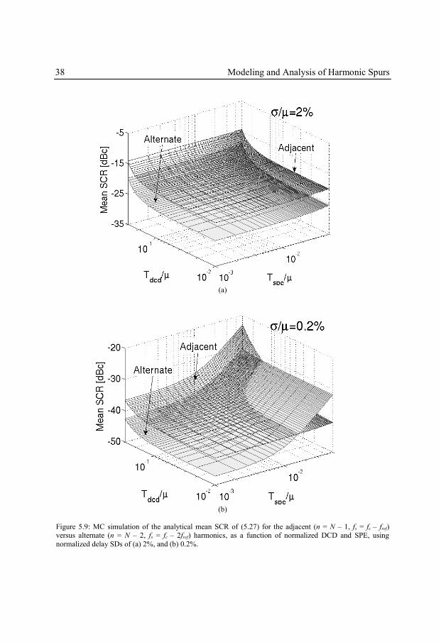
38 Modeling and Analysis of Harmonic Spurs
(a)
(b)
Figure 5.9: MC simulation of the analytical mean SCR of (5.27) for the adjacent (n = N ‒ 1, fs = fc ‒ fref)
versus alternate (n = N ‒ 2, fs = fc ‒ 2fref) harmonics, as a function of normalized DCD and SPE, using
normalized delay SDs of (a) 2%, and (b) 0.2%.
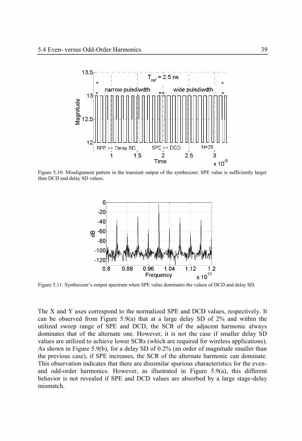
5.4 Even- versus Odd-Order Harmonics 39
The X and Y axes correspond to the normalized SPE and DCD values, respectively. It
can be observed from Figure 5.9(a) that at a large delay SD of 2% and within the
utilized sweep range of SPE and DCD, the SCR of the adjacent harmonic always
dominates that of the alternate one. However, it is not the case if smaller delay SD
values are utilized to achieve lower SCRs (which are required for wireless applications).
As shown in Figure 5.9(b), for a delay SD of 0.2% (an order of magnitude smaller than
the previous case), if SPE increases, the SCR of the alternate harmonic can dominate.
This observation indicates that there are dissimilar spurious characteristics for the even-
and odd-order harmonics. However, as illustrated in Figure 5.9(a), this different
behavior is not revealed if SPE and DCD values are absorbed by a large stage-delay
mismatch.
Figure 5.10: Misalignment pattern in the transient output of the synthesizer; SPE value is sufficiently larger than DCD and delay SD values.
Figure 5.11: Synthesizer’s output spectrum when SPE value dominates the values of DCD and delay SD.
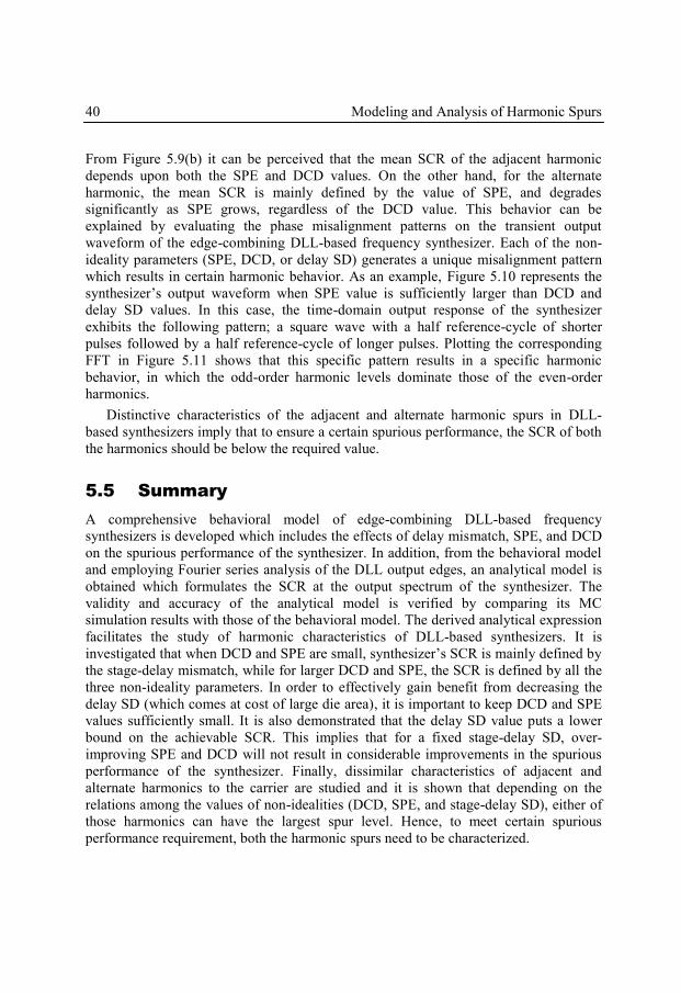
40 Modeling and Analysis of Harmonic Spurs
From Figure 5.9(b) it can be perceived that the mean SCR of the adjacent harmonic
depends upon both the SPE and DCD values. On the other hand, for the alternate
harmonic, the mean SCR is mainly defined by the value of SPE, and degrades
significantly as SPE grows, regardless of the DCD value. This behavior can be
explained by evaluating the phase misalignment patterns on the transient output
waveform of the edge-combining DLL-based frequency synthesizer. Each of the non-
ideality parameters (SPE, DCD, or delay SD) generates a unique misalignment pattern
which results in certain harmonic behavior. As an example, Figure 5.10 represents the
synthesizer’s output waveform when SPE value is sufficiently larger than DCD and
delay SD values. In this case, the time-domain output response of the synthesizer
exhibits the following pattern; a square wave with a half reference-cycle of shorter
pulses followed by a half reference-cycle of longer pulses. Plotting the corresponding
FFT in Figure 5.11 shows that this specific pattern results in a specific harmonic
behavior, in which the odd-order harmonic levels dominate those of the even-order
harmonics.
Distinctive characteristics of the adjacent and alternate harmonic spurs in DLL-
based synthesizers imply that to ensure a certain spurious performance, the SCR of both
the harmonics should be below the required value.
5.5 Summary
A comprehensive behavioral model of edge-combining DLL-based frequency
synthesizers is developed which includes the effects of delay mismatch, SPE, and DCD
on the spurious performance of the synthesizer. In addition, from the behavioral model
and employing Fourier series analysis of the DLL output edges, an analytical model is
obtained which formulates the SCR at the output spectrum of the synthesizer. The
validity and accuracy of the analytical model is verified by comparing its MC
simulation results with those of the behavioral model. The derived analytical expression
facilitates the study of harmonic characteristics of DLL-based synthesizers. It is
investigated that when DCD and SPE are small, synthesizer’s SCR is mainly defined by
the stage-delay mismatch, while for larger DCD and SPE, the SCR is defined by all the
three non-ideality parameters. In order to effectively gain benefit from decreasing the
delay SD (which comes at cost of large die area), it is important to keep DCD and SPE
values sufficiently small. It is also demonstrated that the delay SD value puts a lower
bound on the achievable SCR. This implies that for a fixed stage-delay SD, over-
improving SPE and DCD will not result in considerable improvements in the spurious
performance of the synthesizer. Finally, dissimilar characteristics of adjacent and
alternate harmonics to the carrier are studied and it is shown that depending on the
relations among the values of non-idealities (DCD, SPE, and stage-delay SD), either of
those harmonics can have the largest spur level. Hence, to meet certain spurious
performance requirement, both the harmonic spurs need to be characterized.
41
Chapter 6
Monte Carlo-Free Prediction of
Spurious Performance
6.1 Introduction
The behavioral model of the harmonic spurs at the output spectrum of edge-combining
DLL-based synthesizers was introduced and the corresponding analytical expression
was developed in Chapter 5. It was shown that the magnitude of the harmonic spurs
represented by (5.27) is a random variable defined by the design parameters (reference
frequency ferf and number of DLL phases N), as well as the system non-idealities (SPE,
DCD, and stage-delay SD values). Due to stochastic nature of the mismatch, statistical
simulations such as MC with large number of samples should be performed for accurate
prediction of the spurious performance. However, for such a complex feedback system
which requires a large settling time for each MC sample, circuit-level MC simulations
become extremely cumbersome. Now consider that to satisfy a certain requirement on
the level of harmonic spurs, and to avoid over-sizing the delay stages which leads to
area and speed penalties, optimal device sizes need to be found through an iterative
procedure of improving the circuit parameters and performing a new set of circuit-level
MC simulations to verify the obtained performance. As a result, the overall design time
of the synthesizer is significantly increased.
42 Monte Carlo-Free Prediction of Spurious Performance
This chapter is based [1] and [2], and presents the development of a prediction model
for the harmonic spur levels in edge-combining DLL-based frequency synthesizers.
This model can replace the MC method to significantly speed up the iterative design
procedure of such synthesizers, while providing predictions which are comparable in
terms of robustness and accuracy to that of the MC method. The model is developed by
further expanding the analytical model of the synthesizer in Chapter 5, through Taylor
series approximation and moment methods. As a result, closed-form expressions are
derived for the mean value and probability density function (PDF) of the synthesizer’s
SCR. Validity, accuracy, and robustness of the proposed prediction method against
wide-range values of non-idealities are investigated and verified through MC
simulations of the behavioral model as well as the transistor-level model of the
synthesizer in a standard 65-nm CMOS technology.
Section 6.2 introduces the prediction model based on the properties of Rayleigh
random variables. In Section 6.3, the limitations of the Rayleigh-based model are
discussed and a more generic model is accordingly developed in Section 6.4. Section
6.5 addresses the effect of noise on the level of harmonic spurs and the prediction
accuracy. The chapter is finally summarized in Section 6.6.
6.2 Rayleigh-Based Prediction Model
6.2.1 Spur Magnitude
Provided that the harmonic Fourier coefficients an and bn of the EC output signal,
represented by (5.22) and (5.23), are two independently and identically distributed (iid)
Gaussian random variables with zero mean and equal variances σ2cof, i.e.,
),0(~
),0(~
2
2
cofn
cofn
b
a
, Nn (6.1)
the spur magnitude 22
nnn baS will exhibit a Rayleigh distribution [75]. Assuming
an and bn are independent, if the criteria of (6.1) are satisfied, the harmonic spurs of the
synthesizer can be efficiently characterize using the properties of Rayleigh random
variables. To investigate (6.1), the normality test is performed first. For these
simulations, fref = 400 MHz, N = 25, n = N – 1, Tdcd = 10 ps, Tspe = 1 ps, and σr /µ = σf /µ
= 1 ps, unless otherwise mentioned. The statistical approach for normality test involves
calculation of skewness and kurtosis of the Fourier coefficients. The graphical
approach, on the other hand, has less complexity, and therefore, has been employed
here. Using (5.22) and (5.23), the MC histograms of the harmonic Fourier coefficients
(n = N ± 1) are plotted in Figure 6.1(a), indicating that an fits well within its
corresponding Gaussian fitting curve. The observed skew in bn histogram is due to the
mismatch-averaging characteristic of the DLL, which was discussed in Section 5.2 and
represented by (5.5) and (5.6). This can be verified by re-plotting the histograms for the
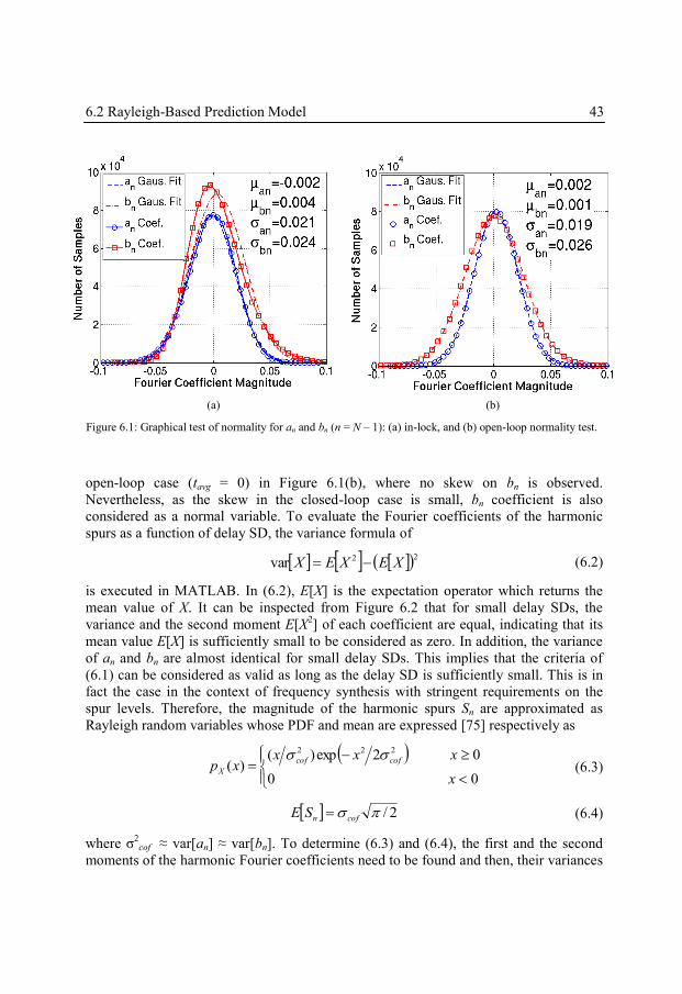
6.2 Rayleigh-Based Prediction Model 43
open-loop case (tavg = 0) in Figure 6.1(b), where no skew on bn is observed.
Nevertheless, as the skew in the closed-loop case is small, bn coefficient is also
considered as a normal variable. To evaluate the Fourier coefficients of the harmonic
spurs as a function of delay SD, the variance formula of
22var XEXEX (6.2)
is executed in MATLAB. In (6.2), E[X] is the expectation operator which returns the
mean value of X. It can be inspected from Figure 6.2 that for small delay SDs, the
variance and the second moment E[X2] of each coefficient are equal, indicating that its
mean value E[X] is sufficiently small to be considered as zero. In addition, the variance
of an and bn are almost identical for small delay SDs. This implies that the criteria of
(6.1) can be considered as valid as long as the delay SD is sufficiently small. This is in
fact the case in the context of frequency synthesis with stringent requirements on the
spur levels. Therefore, the magnitude of the harmonic spurs Sn are approximated as
Rayleigh random variables whose PDF and mean are expressed [75] respectively as
00
02exp)()(
222
x
xxxxp
cofcof
X
(6.3)
2/ cofnSE (6.4)
where σ2
cof ≈ var[an] ≈ var[bn]. To determine (6.3) and (6.4), the first and the second
moments of the harmonic Fourier coefficients need to be found and then, their variances
(a) (b)
Figure 6.1: Graphical test of normality for an and bn (n = N – 1): (a) in-lock, and (b) open-loop normality test.
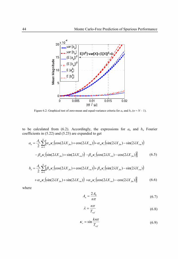
44 Monte Carlo-Free Prediction of Spurious Performance
to be calculated from (6.2). Accordingly, the expressions for an and bn Fourier
coefficients in (5.22) and (5.23) are expanded to get
)2sin()2sin()2cos()2cos(2 1
rmfmcm
N
m
rmfmsmn
n XXXXA
a
)2cos()2cos()2sin()2sin( fmrmcmrmfmsm XXXX (6.5)
)2sin()2sin()2cos()2cos(2 1
rmfmcm
N
m
rmfmsmn
n XXXXA
b
)2cos()2cos()2sin()2sin( fmrmcmrmfmsm XXXX (6.6)
where
n
AAn
02 (6.7)
refT
n
(6.8)
ref
sT
kn sin
(6.9)
Figure 6.2: Graphical test of zero-mean and equal-variance criteria for an and bn (n = N – 1).
6.2 Rayleigh-Based Prediction Model 45
ref
cT
kn cos
(6.10)
kTT
N
m
T
nsperef
ref
m )(2
cos
(6.11)
kTT
N
m
T
nsperef
ref
m )(2
sin
. (6.12)
Utilizing the first- and second-order Taylor series approximation of sine and cosine
functions in (6.5) and (6.6) leads to
N
m
rmfmcmrmfmsmsmnn XXXXAa1
222
222
rmfmcmrmfmsm XXXX (6.13)
N
m
rmfmcmrmfmsmsmnn XXXXAb1
222
222
rmfmcmrmfmsm XXXX . (6.14)
For an Fourier coefficient in (6.13), the mean is derived from its first moment as
rmfmcm
N
m
rmfmsmsmnn XXEXXEAaE
1
222
222
rmfmcmrmfmsm XXEXXE . (6.15)
To calculate E[an], Xrm and Xfm from (5.24) and (5.25) respectively, are first utilized to
write
0 rmrm XEXE (6.16)
22 )1( rrmN
mmXE (6.17)
)( 222
rffmN
mmXE . (6.18)
Afterwards, the required expectations by (6.15) are calculated using linearity as
0 rmfmrmfm XXEXXE (6.19)
46 Monte Carlo-Free Prediction of Spurious Performance
2222
rfrmfm mXXE (6.20)
)1
2(2222
N
mmXXE rfrmfm . (6.21)
By substitution of (6.19), (6.20), and (6.21) into (6.15), E[an] is calculated. Performing a
similar analysis for (6.14), E[bn] is also calculated. As a result,
)12
()( 222
1
222
N
mmmAaE rfcm
N
m
rfsmsmnn (6.22)
N
m
rfcmrfsmsmnnN
mmmAbE
1
222222 )12
()( . (6.23)
To obtain an variance, (E[an])2 and E[an
2] are required. The former is determined
directly from (6.15). The latter is derived by calculating an2 from (6.13) and applying
the expectation function. Next, the calculated (E[an])2
and E[an2] are substituted to the
variance formula of (6.2) to find an variance. This can be similarly done for bn. The
corresponding mathematical analysis has been provided in details in the Appendix.
After all the calculations and simplifications, the following results are obtained.
1
1 11
22222 2)()(varN
m
N
mi
im
N
m
mrfcnn mmAa
1
1 11
2222 2)(N
m
N
mi
im
N
m
mrfs mm
N
mi
rfi
m
i
rfi
N
m
mcsN
im
N
mi
1
22
1
22
1
)12
()12
(2 . (6.24)
1
1 11
22222 2)()(varN
m
N
mi
im
N
m
mrfcnn mmAb
1
1 11
2222 2)(N
m
N
mi
im
N
m
mrfs mm
N
mi
rfi
m
i
rfi
N
m
mcsN
im
N
mi
1
22
1
22
1
)12
()12
(2 . (6.25)
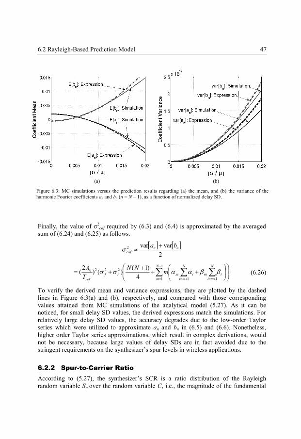
6.2 Rayleigh-Based Prediction Model 47
Finally, the value of σ2
cof required by (6.3) and (6.4) is approximated by the averaged
sum of (6.24) and (6.25) as follows.
2
varvar2 nncof
ba
N
mi
im
N
mi
im
N
m
rf
ref
mNN
T
A
11
1
1
2220
4
)1()()
2( . (6.26)
To verify the derived mean and variance expressions, they are plotted by the dashed
lines in Figure 6.3(a) and (b), respectively, and compared with those corresponding
values attained from MC simulations of the analytical model (5.27). As it can be
noticed, for small delay SD values, the derived expressions match the simulations. For
relatively large delay SD values, the accuracy degrades due to the low-order Taylor
series which were utilized to approximate an and bn in (6.5) and (6.6). Nonetheless,
higher order Taylor series approximations, which result in complex derivations, would
not be necessary, because large values of delay SDs are in fact avoided due to the
stringent requirements on the synthesizer’s spur levels in wireless applications.
6.2.2 Spur-to-Carrier Ratio
According to (5.27), the synthesizer’s SCR is a ratio distribution of the Rayleigh
random variable Sn over the random variable C, i.e., the magnitude of the fundamental
(a) (b)
Figure 6.3: MC simulations versus the prediction results regarding (a) the mean, and (b) the variance of the harmonic Fourier coefficients an and bn (n = N – 1), as a function of normalized delay SD.
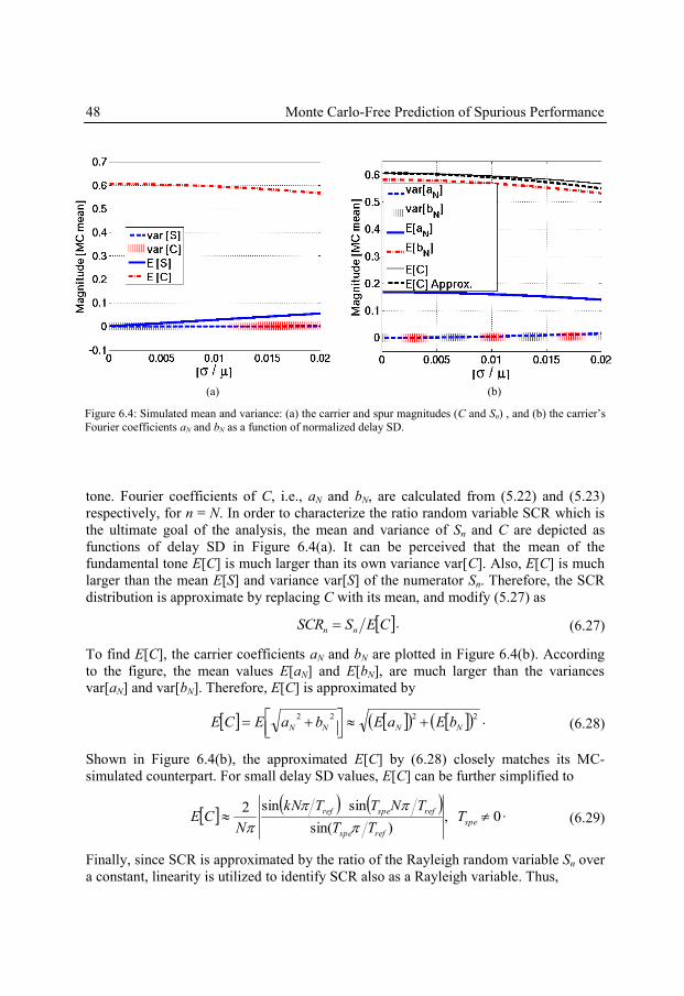
48 Monte Carlo-Free Prediction of Spurious Performance
tone. Fourier coefficients of C, i.e., aN and bN, are calculated from (5.22) and (5.23)
respectively, for n = N. In order to characterize the ratio random variable SCR which is
the ultimate goal of the analysis, the mean and variance of Sn and C are depicted as
functions of delay SD in Figure 6.4(a). It can be perceived that the mean of the
fundamental tone E[C] is much larger than its own variance var[C]. Also, E[C] is much
larger than the mean E[S] and variance var[S] of the numerator Sn. Therefore, the SCR
distribution is approximate by replacing C with its mean, and modify (5.27) as
CESSCR nn . (6.27)
To find E[C], the carrier coefficients aN and bN are plotted in Figure 6.4(b). According
to the figure, the mean values E[aN] and E[bN], are much larger than the variances
var[aN] and var[bN]. Therefore, E[C] is approximated by
2222
NNNN bEaEbaECE
. (6.28)
Shown in Figure 6.4(b), the approximated E[C] by (6.28) closely matches its MC-
simulated counterpart. For small delay SD values, E[C] can be further simplified to
0,)sin(
sinsin2 spe
refspe
refsperefT
TT
TNTTkN
NCE
. (6.29)
Finally, since SCR is approximated by the ratio of the Rayleigh random variable Sn over
a constant, linearity is utilized to identify SCR also as a Rayleigh variable. Thus,
(a) (b)
Figure 6.4: Simulated mean and variance: (a) the carrier and spur magnitudes (C and Sn) , and (b) the carrier’s
Fourier coefficients aN and bN as a function of normalized delay SD.
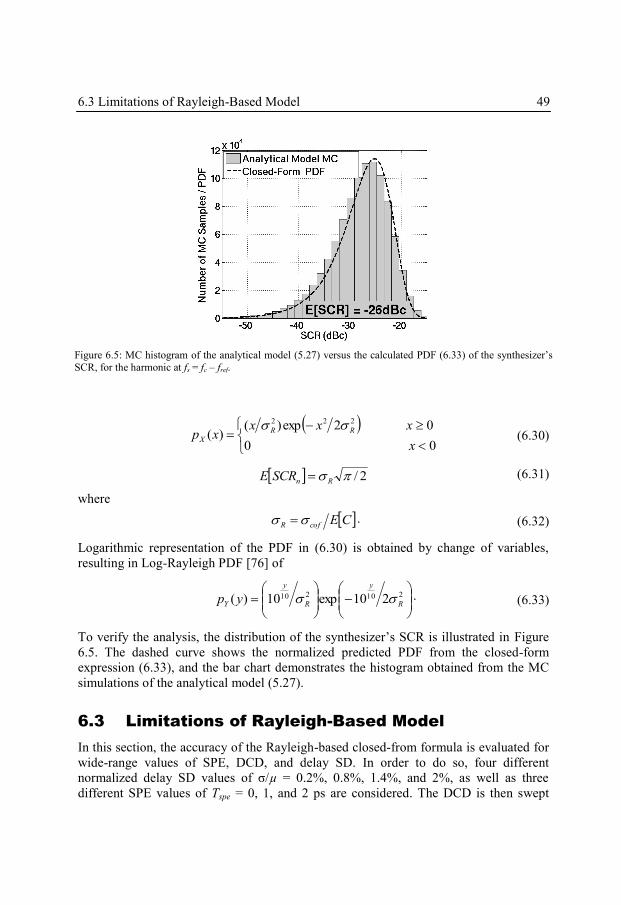
6.3 Limitations of Rayleigh-Based Model 49
00
02exp)()(
222
x
xxxxp RR
X
(6.30)
2/ RnSCRE (6.31)
where
CEcofR . (6.32)
Logarithmic representation of the PDF in (6.30) is obtained by change of variables,
resulting in Log-Rayleigh PDF [76] of
210210 210exp10)( R
y
R
y
Y yp . (6.33)
To verify the analysis, the distribution of the synthesizer’s SCR is illustrated in Figure
6.5. The dashed curve shows the normalized predicted PDF from the closed-form
expression (6.33), and the bar chart demonstrates the histogram obtained from the MC
simulations of the analytical model (5.27).
6.3 Limitations of Rayleigh-Based Model
In this section, the accuracy of the Rayleigh-based closed-from formula is evaluated for
wide-range values of SPE, DCD, and delay SD. In order to do so, four different
normalized delay SD values of σ/µ = 0.2%, 0.8%, 1.4%, and 2%, as well as three
different SPE values of Tspe = 0, 1, and 2 ps are considered. The DCD is then swept
Figure 6.5: MC histogram of the analytical model (5.27) versus the calculated PDF (6.33) of the synthesizer’s
SCR, for the harmonic at fs = fc – fref.
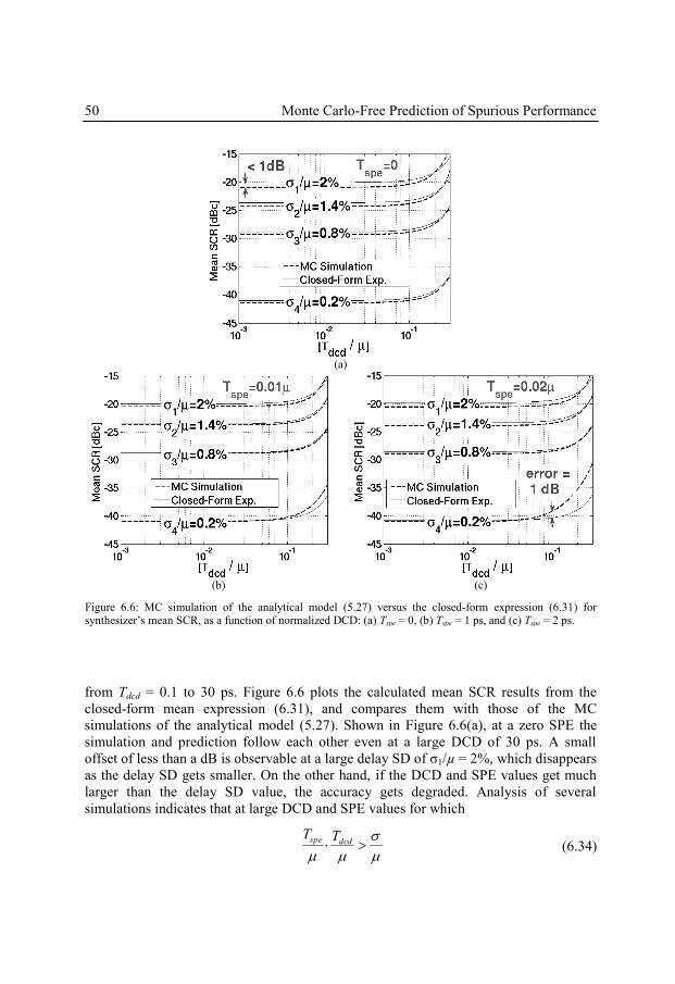
50 Monte Carlo-Free Prediction of Spurious Performance
from Tdcd = 0.1 to 30 ps. Figure 6.6 plots the calculated mean SCR results from the
closed-form mean expression (6.31), and compares them with those of the MC
simulations of the analytical model (5.27). Shown in Figure 6.6(a), at a zero SPE the
simulation and prediction follow each other even at a large DCD of 30 ps. A small
offset of less than a dB is observable at a large delay SD of σ1/µ = 2%, which disappears
as the delay SD gets smaller. On the other hand, if the DCD and SPE values get much
larger than the delay SD value, the accuracy gets degraded. Analysis of several
simulations indicates that at large DCD and SPE values for which
dcdspe TT
(6.34)
(a)
(b) (c)
Figure 6.6: MC simulation of the analytical model (5.27) versus the closed-form expression (6.31) for synthesizer’s mean SCR, as a function of normalized DCD: (a) Tspe = 0, (b) Tspe = 1 ps, and (c) Tspe = 2 ps.
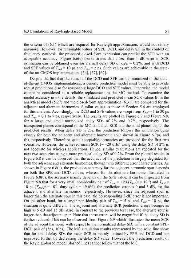
6.3 Limitations of Rayleigh-Based Model 51
the criteria of (6.1) which are required for Rayleigh approximation, would not satisfy
anymore. However, for reasonable values of SPE, DCD, and delay SD in the context of
frequency synthesis, the proposed closed-form expression can predict the SCR with an
acceptable accuracy. Figure 6.6(c) demonstrates that a less than 1 dB error in SCR
estimation can be obtained even for a small delay SD of σ4/µ = 0.2%, and with DCD
and SPE values of Tdcd = 10 ps and Tspe = 2 ps. Such values are achievable in the state-
of-the-art CMOS implementations [54], [57], [62].
Despite the fact that the values of the DCD and SPE can be minimized in the state-
of-the-art CMOS implementations, a generic prediction model must be able to provide
robust predictions also for reasonably large DCD and SPE values. Otherwise, the model
cannot be considered as a reliable replacement to the MC method. To examine the
model accuracy in more details, the simulated and predicted mean SCR values from the
analytical model (5.27) and the closed-form approximation (6.31), are compared for the
adjacent and alternate harmonics. Similar values as those in Section 5.4 are employed
for this analysis. Accordingly, the DCD and SPE values are swept from Tdcd = 1 to 30 ps
and Tspe = 0.1 to 5 ps, respectively. The results are plotted in Figure 6.7 and Figure 6.8,
for a large and small normalized delay SDs of 2% and 0.2%, respectively. The
transparent planes correspond to the MC-simulated SCR and the solid planes depict the
predicted results. When delay SD is 2%, the prediction follows the simulation quite
closely for both the adjacent and alternate harmonic spur shown in Figure 6.7(a) and
(b), respectively. Therefore, quite acceptable accuracies are provided for the first two
scenarios. However, the achieved mean SCR (~ ‒20 dBc) using the delay SD of 2% is
not adequate for wireless applications. Hence, similar evaluations are repeated for the
next two scenarios using a more practical delay SD of 0.2%. From the plotted results in
Figure 6.8 it can be observed that the accuracy of the prediction is largely degraded for
both the adjacent and alternate harmonics, though with different error characteristics. As
shown in Figure 6.8(a), the prediction accuracy for the adjacent harmonic spur depends
on both the SPE and DCD values, whereas for the alternate harmonic illustrated in
Figure 6.8(b), the accuracy mainly depends on the SPE value. It can be inspected from
Figure 6.8 that for a very small non-ideality pair of Tspe = 1 ps (Tspe/µ = 10-2
) and Tdcd =
10 ps (Tdcd/µ = 10-1
, duty cycle = 49.6%), the prediction error is 0 and 3 dB, for the
adjacent and alternate harmonics, respectively. However, since the adjacent spur is
larger than the alternate spur in this case, the corresponding 3-dB error is not important.
On the other hand, for a larger non-ideality pair of Tspe = 5 ps and Tdcd = 10 ps, the
situation is quite different. The adjacent and alternate SCR prediction errors become as
high as 5 dB and 15 dB. Also, in contrast to the previous test case, the alternate spur is
larger than the adjacent spur. Note that these errors will be magnified if the delay SD is
further reduced. This can be observed from Figure 6.9 which illustrates the mean SCR
of the adjacent harmonic with respect to the normalized delay SD, with a constant SPE-
DCD pair of (5ps, 10ps). The MC simulation results represented by the solid line show
that for small delay SDs the mean SCR is mainly defined by SPE and DCD and not
improved further by decreasing the delay SD value. However, the prediction results of
the Rayleigh-based model (dashed line) cannot follow that of the MC.
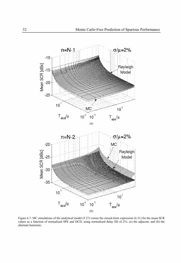
52 Monte Carlo-Free Prediction of Spurious Performance
(a)
(b)
Figure 6.7: MC simulations of the analytical model (5.27) versus the closed-form expression (6.31) for the mean SCR
values as a function of normalized SPE and DCD, using normalized delay SD of 2%: (a) the adjacent, and (b) the alternate harmonic.
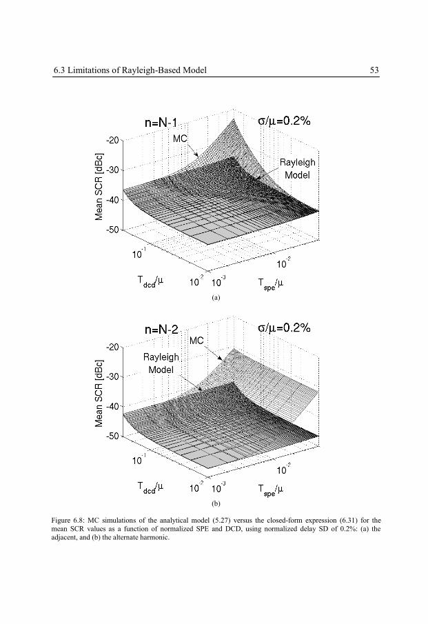
6.3 Limitations of Rayleigh-Based Model 53
(a)
(b)
Figure 6.8: MC simulations of the analytical model (5.27) versus the closed-form expression (6.31) for the
mean SCR values as a function of normalized SPE and DCD, using normalized delay SD of 0.2%: (a) the
adjacent, and (b) the alternate harmonic.
54 Monte Carlo-Free Prediction of Spurious Performance
Apart from its conditional accuracy, there is another limiting factor concerning this
model. It can be concluded by comparing Figure 6.7 and Figure 6.8 that the accuracy
conditions are defined by the relations among the values of delay SD, SPE, and DCD.
This makes it complicated to define those conditions and bounds in such a generic form
that can be utilized for every design scenario without needing to perform case-specific
simulations. This indicates that it is of great importance to develop a more generic
prediction model for SCR estimation in edge-combining DLL-based frequency
synthesizers, whose accuracy is independent from the practical values of the design
parameters and system non-idealities. Such a model should provide predictions that are
as robust as those achieved using statistical simulations, and hence, can be employed as
a general replacement to MC method.
6.4 Generic Ricean-Based Prediction Model
Different approaches can be employed to find a more accurate PDF than (6.30) for the
SCR random variable of (5.27). An exact solution would be to derive the PDF of
Fourier coefficients directly from the random non-idealities and then, by transformation
of the resulting PDFs into their root sum square, calculate the PDF of SCR. Deriving the
PDF of an and bn in (6.13) and (6.14) respectively, requires calculation of the PDF for
the elements of an and bn which are in form of time series and would result in complex
analysis. In order to avoid dealing with complicated derivations involved in the direct
PDF transformation method, another approach is employed here. The idea is to
Figure 6.9: MC simulation of the analytical model (5.27) versus the closed-form expression (6.31) for mean SCR as a function of normalized delay SD.
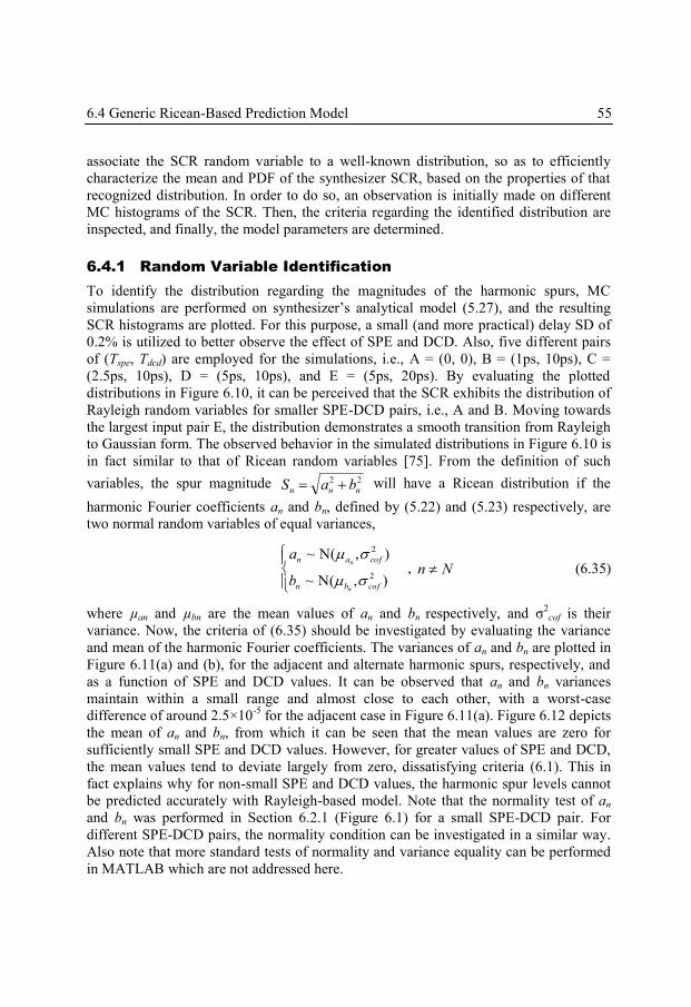
6.4 Generic Ricean-Based Prediction Model 55
associate the SCR random variable to a well-known distribution, so as to efficiently
characterize the mean and PDF of the synthesizer SCR, based on the properties of that
recognized distribution. In order to do so, an observation is initially made on different
MC histograms of the SCR. Then, the criteria regarding the identified distribution are
inspected, and finally, the model parameters are determined.
6.4.1 Random Variable Identification
To identify the distribution regarding the magnitudes of the harmonic spurs, MC
simulations are performed on synthesizer’s analytical model (5.27), and the resulting
SCR histograms are plotted. For this purpose, a small (and more practical) delay SD of
0.2% is utilized to better observe the effect of SPE and DCD. Also, five different pairs
of (Tspe, Tdcd) are employed for the simulations, i.e., A = (0, 0), B = (1ps, 10ps), C =
(2.5ps, 10ps), D = (5ps, 10ps), and E = (5ps, 20ps). By evaluating the plotted
distributions in Figure 6.10, it can be perceived that the SCR exhibits the distribution of
Rayleigh random variables for smaller SPE-DCD pairs, i.e., A and B. Moving towards
the largest input pair E, the distribution demonstrates a smooth transition from Rayleigh
to Gaussian form. The observed behavior in the simulated distributions in Figure 6.10 is
in fact similar to that of Ricean random variables [75]. From the definition of such
variables, the spur magnitude 22
nnn baS will have a Ricean distribution if the
harmonic Fourier coefficients an and bn, defined by (5.22) and (5.23) respectively, are
two normal random variables of equal variances,
),(~
),(~
2
2
cofbn
cofan
n
n
b
a
, Nn (6.35)
where µan and µbn are the mean values of an and bn respectively, and σ2cof is their
variance. Now, the criteria of (6.35) should be investigated by evaluating the variance
and mean of the harmonic Fourier coefficients. The variances of an and bn are plotted in
Figure 6.11(a) and (b), for the adjacent and alternate harmonic spurs, respectively, and
as a function of SPE and DCD values. It can be observed that an and bn variances
maintain within a small range and almost close to each other, with a worst-case
difference of around 2.5×10⁻⁵
for the adjacent case in Figure 6.11(a). Figure 6.12 depicts
the mean of an and bn, from which it can be seen that the mean values are zero for
sufficiently small SPE and DCD values. However, for greater values of SPE and DCD,
the mean values tend to deviate largely from zero, dissatisfying criteria (6.1). This in
fact explains why for non-small SPE and DCD values, the harmonic spur levels cannot
be predicted accurately with Rayleigh-based model. Note that the normality test of an
and bn was performed in Section 6.2.1 (Figure 6.1) for a small SPE-DCD pair. For
different SPE-DCD pairs, the normality condition can be investigated in a similar way.
Also note that more standard tests of normality and variance equality can be performed
in MATLAB which are not addressed here.
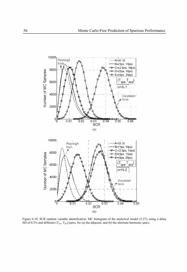
56 Monte Carlo-Free Prediction of Spurious Performance
(a)
(b)
Figure 6.10: SCR random variable identification: MC histogram of the analytical model (5.27), using a delay
SD of 0.2% and different (Tspe, Tdcd) pairs, for (a) the adjacent, and (b) the alternate harmonic spurs.
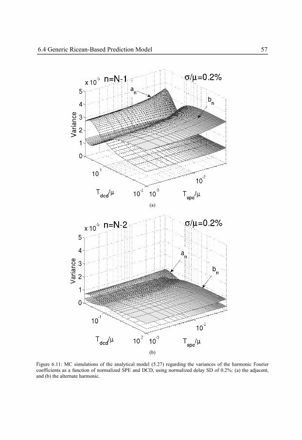
6.4 Generic Ricean-Based Prediction Model 57
(a)
(b)
Figure 6.11: MC simulations of the analytical model (5.27) regarding the variances of the harmonic Fourier
coefficients as a function of normalized SPE and DCD, using normalized delay SD of 0.2%: (a) the adjacent, and (b) the alternate harmonic.
58 Monte Carlo-Free Prediction of Spurious Performance
(a)
(b)
Figure 6.12: MC simulations of the analytical model (5.27) regarding the mean values of the harmonic Fourier coefficients as a function of normalized SPE and DCD, using normalized delay SD of 0.2%: (a) the adjacent,
and (b) the alternate harmonic.
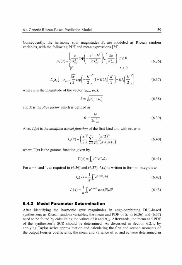
6.4 Generic Ricean-Based Prediction Model 59
Consequently, the harmonic spur magnitudes Sn are modeled as Ricean random
variables, with the following PDF and mean expressions [75].
00
02
exp)( 202
22
2
z
zhz
Ihzz
zpcofcofcofZ
(6.36)
22)1(
2exp
210
KKI
KIK
KSE cofn
(6.37)
where h is the magnitude of the vector (µan, µbn),
22
nn bah (6.38)
and K is the Rice factor which is defined as
2
2
2 cof
hK
. (6.39)
Also, Iα(x) is the modified Bessel function of the first kind and with order α,
0
2
1!
2/
2)(
p
p
pp
xxxI
(6.40)
where Γ(x) is the gamma function given by
0
1)( dtetx tx . (6.41)
For α = 0 and 1, as required in (6.36) and (6.37), Iα(x) is written in form of integrals as
0
cos
0
1)( dexI x (6.42)
0
cos
1 )cos(1
)( dexI x . (6.43)
6.4.2 Model Parameter Determination
After identifying the harmonic spur magnitudes in edge-combining DLL-based
synthesizers as Ricean random variables, the mean and PDF of Sn in (6.36) and (6.37)
need to be found by calculating the values of h and σcof. Afterwards, the mean and PDF
of the synthesizer’s SCR should be determined. As discussed in Section 6.2.1, by
applying Taylor series approximation and calculating the first and second moments of
the output Fourier coefficients, the mean and variance of an and bn were determined in
60 Monte Carlo-Free Prediction of Spurious Performance
(6.22) ‒ (6.25). The value of h can be found by substitution of the numerical values of
µan and µbn from (6.22) and (6.23) into (6.38). Also, σcof is calculated from (6.26). Now,
knowing the Ricean random variable Sn, the ratio random variable SCRn defined by
(5.27) should be determined. As discussed in Section 6.2.2, it can be shown that the
random variable C which represents the carrier magnitude, can be approximated by its
mean value E[C], and hence, (5.27) is simplified to SCRn = Sn / E[C]. This effectively
means that the harmonic Fourier coefficients of Sn (an and bn) are divided by a constant
to form the Fourier coefficients of SCRn,
),(~ 2
cofan na Nn (6.44)
),(~ 2
cofbn nb Nn (6.45)
where from linearity,
CE
n
n
a
a
(6.46)
CE
n
n
b
b
(6.47)
2
2
2
CE
cof
cof
. (6.48)
Hence, SCRn is also a Ricean variable with the following mean and PDF
00
02
exp)( 202
22
2
z
zzh
Ihzz
zpcofcofcofZ
(6.49)
22)1(
2exp
210
KIK
KIK
KSCRE cofn
(6.50)
where
CE
hh
nn ba 22 (6.51)
Khh
Kcofcof
2
2
2
2
22 . (6.52)
Note that as implied by (6.52), unlike the other model parameters, i.e., h and σcof, the
Rice factor remains equal for both Ricean random variables Sn and SCRn.
6.4 Generic Ricean-Based Prediction Model 61
6.4.3 Behavioral Validation
The mean SCR of the synthesizer in (6.50) is plotted in Figure 6.13 and Figure 6.14 as a
function of SPE and DCD, using a normalized delay SD of 2% and 0.2%, respectively.
Figure 6.13(a) and Figure 6.14(a) demonstrate the adjacent harmonic spur levels at fs =
fc ‒ fref while Figure 6.13(b) and Figure 6.14(b) illustrate the alternate harmonic levels at
fs = fc ‒ 2fref. The solid planes represent the MC simulation results of the analytical
model (5.27), whereas the solid lines with markers depict the predicted mean SCR
provided by (6.50). It can be verified from Figure 6.13 and Figure 6.14 that the
prediction results closely follow that of the MC simulations, for wide-range values of
SPE and DCD. In order to verify the accuracy of the model also against wide-range
delay SD values, the mean SCR is plotted in Figure 6.15 with respect to the normalized
delay SD which is swept from 0.01% to 5%. The prediction and simulation results are
closely matched with an error of 0 dB for σ/µ = 0.01% to 1%, 1 dB at σ/µ = 2%, and 2
dB at σ/µ = 3% (SCRmean ≈ ‒15 dB). Note that to improve the prediction accuracy for
very large delay SD values, higher order Taylor series can be employed to approximate
sine and cosine functions in (6.5) and (6.6) more accurately, and hence, calculate the
more exact model parameters, i.e., the mean and variance of an and bn in (6.22) ‒
(6.25). Nonetheless, as it was also explained previously, large delay SD values are in
fact avoided due to the stringent requirements on the output spur levels in wireless
applications. Comparing the results in Figure 6.13, Figure 6.14 and Figure 6.15 with
those in Figure 6.7, Figure 6.8 and Figure 6.9, respectively, reveals the achieved
improvements in the SCR prediction robustness for both the even- and odd-order
harmonics, against wide-range values of SPE, DCD, and delay SD.
6.4.4 Transistor-Level Validation
It was shown in Section 6.4.3 that the prediction model closely matches the behavioral
model of the DLL-based synthesizer in SCR estimation, over wide-range values of non-
idealities. In this section, the validity and accuracy of the prediction models are
investigated by comparing the PDFs from the closed-form expression (6.30) and (6.49),
with MC simulation histograms of a transistor-level model of the synthesizer which is
designed in a standard 65-nm CMOS process. Note that due to the large simulation time
which is involved in MC simulations of the transistor-level design, it is not affordable to
simulate the SCR over wide-range values of SPE and DCD. As a consequence, three
different pairs of (Tspe, Tdcd) are instead selected for this experiment. Also note that the
reported SCR values in this part correspond to the largest adjacent and alternate
harmonics, i.e., max(SCRN‒1, SCRN+1) for the adjacent, and max(SCRN‒2, SCRN+2) for the
alternate harmonic. The simulated model of the edge-combining DLL-based synthesizer
is shown in Figure 6.16 where 25 output phases of the VCDL are combined using 25
ideal stages of V-I converters to generate the fundamental tone at fc = 10 GHz. Note that
in a practical implementation of the synthesizer [35], [36], an LC-tank load can be used
to enhance the output impedance. Depending on the Q factor of the tank, this will also
suppress the spur levels and relax the sideband spur requirement on the synthesizer.
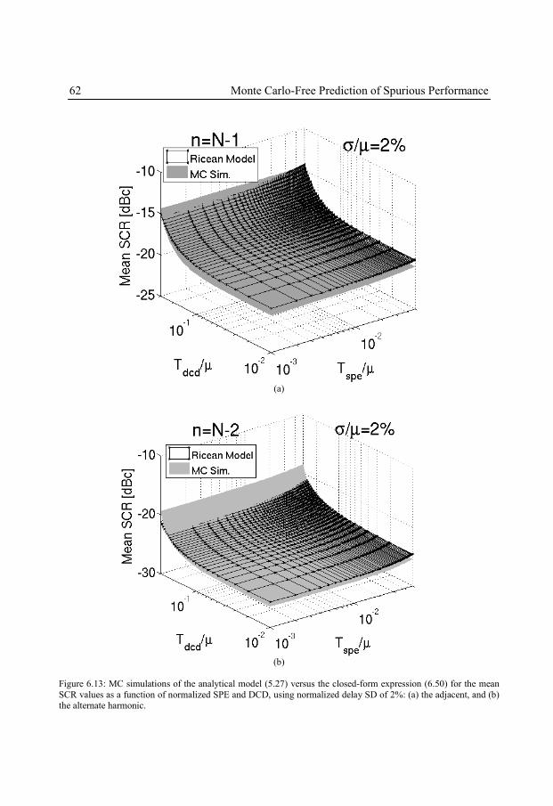
62 Monte Carlo-Free Prediction of Spurious Performance
(a)
(b)
Figure 6.13: MC simulations of the analytical model (5.27) versus the closed-form expression (6.50) for the mean
SCR values as a function of normalized SPE and DCD, using normalized delay SD of 2%: (a) the adjacent, and (b) the alternate harmonic.
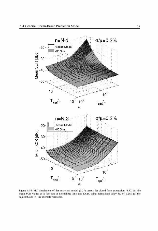
6.4 Generic Ricean-Based Prediction Model 63
(a)
(b)
Figure 6.14: MC simulations of the analytical model (5.27) versus the closed-form expression (6.50) for the mean SCR values as a function of normalized SPE and DCD, using normalized delay SD of 0.2%: (a) the
adjacent, and (b) the alternate harmonic.
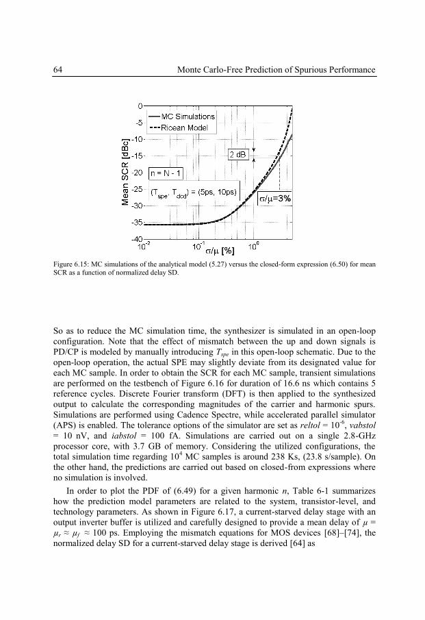
64 Monte Carlo-Free Prediction of Spurious Performance
So as to reduce the MC simulation time, the synthesizer is simulated in an open-loop
configuration. Note that the effect of mismatch between the up and down signals is
PD/CP is modeled by manually introducing Tspe in this open-loop schematic. Due to the
open-loop operation, the actual SPE may slightly deviate from its designated value for
each MC sample. In order to obtain the SCR for each MC sample, transient simulations
are performed on the testbench of Figure 6.16 for duration of 16.6 ns which contains 5
reference cycles. Discrete Fourier transform (DFT) is then applied to the synthesized
output to calculate the corresponding magnitudes of the carrier and harmonic spurs.
Simulations are performed using Cadence Spectre, while accelerated parallel simulator
(APS) is enabled. The tolerance options of the simulator are set as reltol = 10-6
, vabstol
= 10 nV, and iabstol = 100 fA. Simulations are carried out on a single 2.8-GHz
processor core, with 3.7 GB of memory. Considering the utilized configurations, the
total simulation time regarding 104 MC samples is around 238 Ks, (23.8 s/sample). On
the other hand, the predictions are carried out based on closed-from expressions where
no simulation is involved.
In order to plot the PDF of (6.49) for a given harmonic n, Table 6-1 summarizes
how the prediction model parameters are related to the system, transistor-level, and
technology parameters. As shown in Figure 6.17, a current-starved delay stage with an
output inverter buffer is utilized and carefully designed to provide a mean delay of µ =
µr ≈ µf ≈ 100 ps. Employing the mismatch equations for MOS devices [68]‒[74], the
normalized delay SD for a current-starved delay stage is derived [64] as
Figure 6.15: MC simulations of the analytical model (5.27) versus the closed-form expression (6.50) for mean SCR as a function of normalized delay SD.
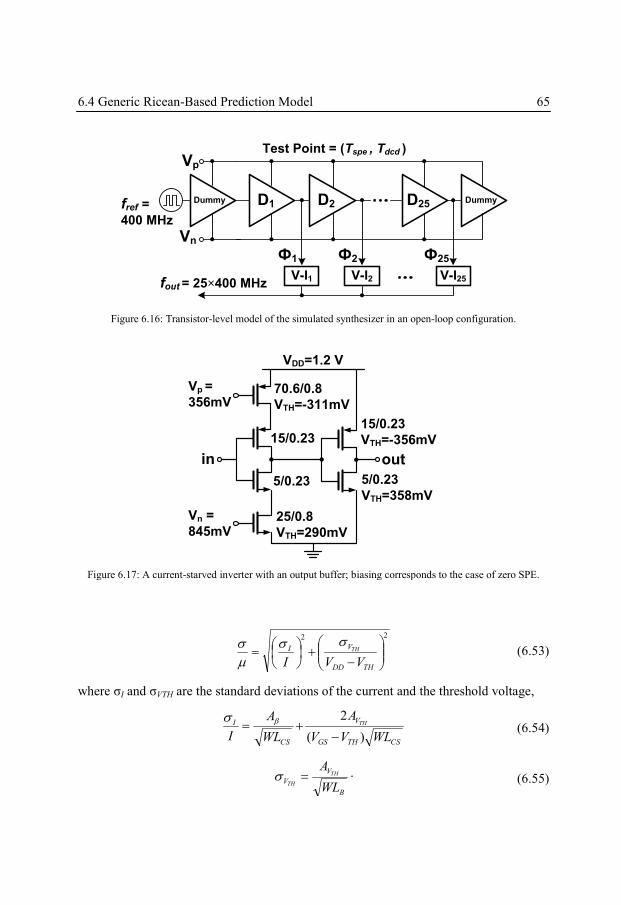
6.4 Generic Ricean-Based Prediction Model 65
22
THDD
VI
VVITH
(6.53)
where σI and σVTH are the standard deviations of the current and the threshold voltage,
CSTHGS
V
CS
I
WLVV
A
WL
A
ITH
)(
2
(6.54)
B
V
VWL
ATH
TH . (6.55)
Dummy D1 D25 Dummy
Ф1 Ф25
V-I25V-I1
D2
Ф2
V-I2
Vp
Vn
fref =
400 MHz
fout = 25×400 MHz
Test Point = (Tspe , Tdcd )
Figure 6.16: Transistor-level model of the simulated synthesizer in an open-loop configuration.
Vp =
356mV
in out
70.6/0.8
VTH=-311mV
Vn =
845mV
15/0.2315/0.23
VTH=-356mV
5/0.23
VTH=358mV5/0.23
25/0.8
VTH=290mV
VDD=1.2 V
Figure 6.17: A current-starved inverter with an output buffer; biasing corresponds to the case of zero SPE.
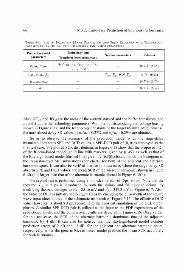
66 Monte Carlo-Free Prediction of Spurious Performance
Also, WLCS and WLB are the areas of the current-starved and the buffer transistors, and
Aβ and AVTH are the technology parameters. With the transistor sizing and voltage biasing
shown in Figure 6.17, and the technology constants of the target 65 nm CMOS process,
the normalized delay SD values of σr /µr ≈ 0.27% and σf /µf ≈ 0.29% are obtained.
So as to observe the accuracy of the prediction model when the stage-delay
mismatch dominates SPE and DCD values, a SPE-DCD pair of (0, 0) is employed as the
first test case. The plotted SCR distributions in Figure 6.18 show that the proposed PDF
of the Ricean-based model (solid line with markers) given by (6.49), as well as that of
the Rayleigh-based model (dashed line) given by (6.30), closely match the histogram of
the transistor-level MC simulations (bar chart), for both of the adjacent and alternate
harmonic spurs. It can also be verified that for this test case, where the stage-delay SD
absorbs SPE and DCD values, the mean SCR of the adjacent harmonic, shown in Figure
6.18(a), is larger than that of the alternate harmonic plotted in Figure 6.18(b).
The second test is performed using a non-ideality pair of (5ps, 9.3ps). Note that the
required Tspe = 5 ps is introduced to both the rising- and falling-edge delays, by
modifying the bias voltages to Vn = 851.6 mV and Vp = 347.3 mV in Figure 6.17. Also,
the value of DCD is initially set to Tdcd = 10 ps by changing the pulsewidth of the square
wave input clock source in the schematic testbench of Figure 6.16. The effective DCD
value, however, is about 9.3 ps, according to the transient simulation of the DLL output
phases. A similar SPE-DCD pair is utilized as the input to the PDF expressions of the
prediction models, and the comparison results are depicted in Figure 6.19. Observe that
for this test case, the SCR of the alternate harmonic dominates that of the adjacent
harmonic by 4 dB. It can also be noticed that the Rayleigh-based model exhibits
prediction errors of 2 dB and 12 dB, for the adjacent and alternate harmonic spurs,
respectively, while the generic Ricean-based model predicts the mean SCR accurately
for both harmonics.
TABLE 6-1: LIST OF PREDICTION MODEL PARAMETERS AND THEIR RELATIONS WITH TECHNOLOGY
PARAMETERS, TRANSISTOR-LEVEL PARAMETERS, AND SYSTEM PARAMETERS
Prediction model
parameters
Technology and
Transistor-level parameters System parameters Relation
σr /µr, σf /µf σI, σVTH, Aβ, AVTH, VTH, WL,
Vn, Vp, VDD ‒ (6.53) ‒ (6.55)
λ, κc, κs, αm, βm ‒ Tdcd, Tspe, n, N, Tref (6.7) ‒ (6.12)
µan, µbn, σcof ‒ ‒ (6.22) ‒ (6.26)
h, K ‒ ‒ (6.51) ‒ (6.52)
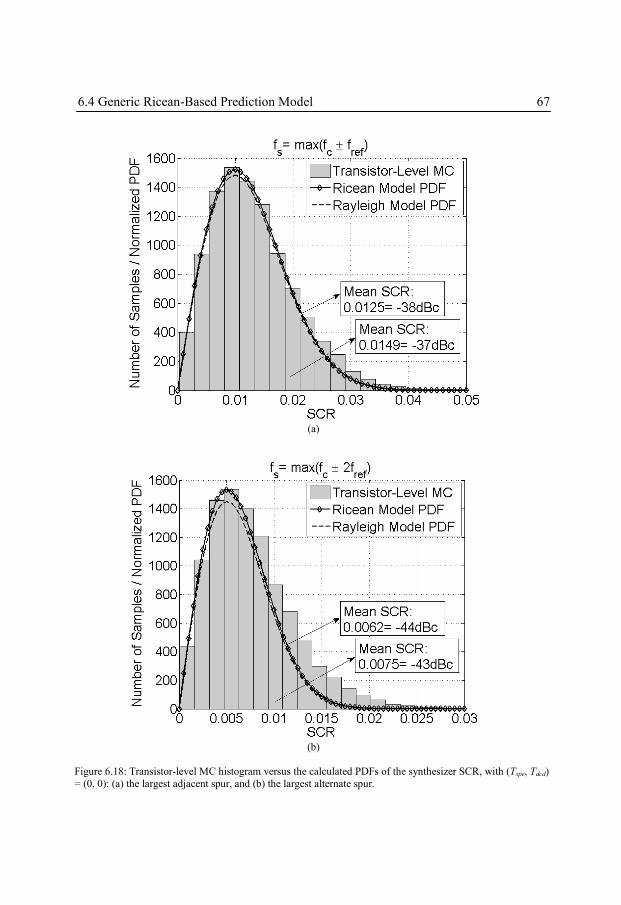
6.4 Generic Ricean-Based Prediction Model 67
(a)
(b)
Figure 6.18: Transistor-level MC histogram versus the calculated PDFs of the synthesizer SCR, with (Tspe, Tdcd)
= (0, 0): (a) the largest adjacent spur, and (b) the largest alternate spur.
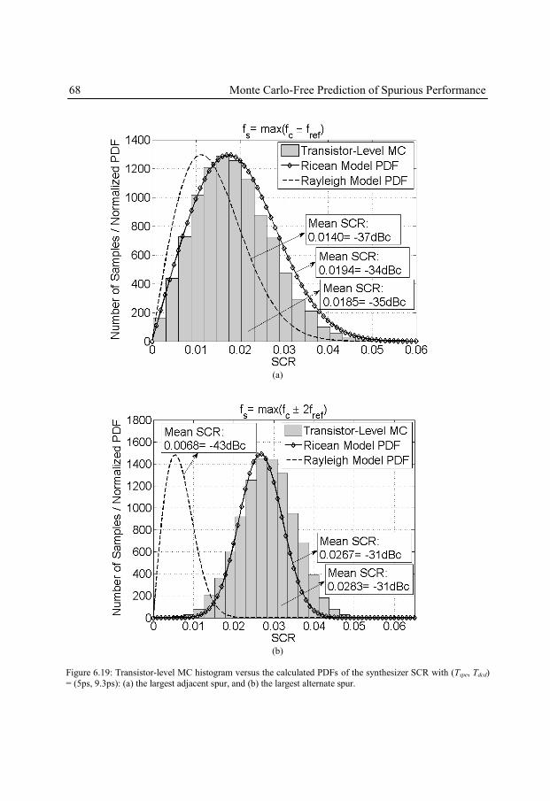
68 Monte Carlo-Free Prediction of Spurious Performance
(a)
(b)
Figure 6.19: Transistor-level MC histogram versus the calculated PDFs of the synthesizer SCR with (Tspe, Tdcd)
= (5ps, 9.3ps): (a) the largest adjacent spur, and (b) the largest alternate spur.
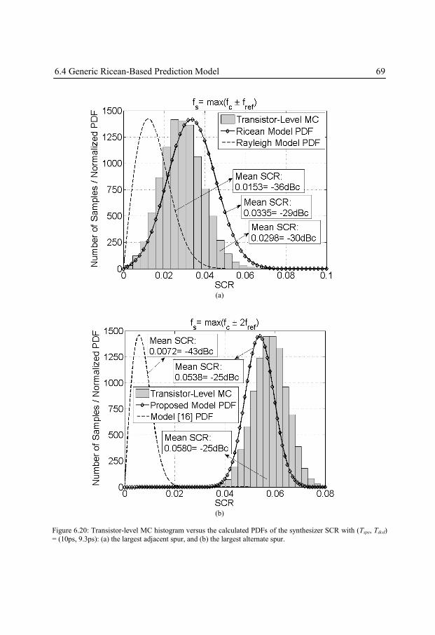
6.4 Generic Ricean-Based Prediction Model 69
(a)
(b)
Figure 6.20: Transistor-level MC histogram versus the calculated PDFs of the synthesizer SCR with (Tspe, Tdcd)
= (10ps, 9.3ps): (a) the largest adjacent spur, and (b) the largest alternate spur.
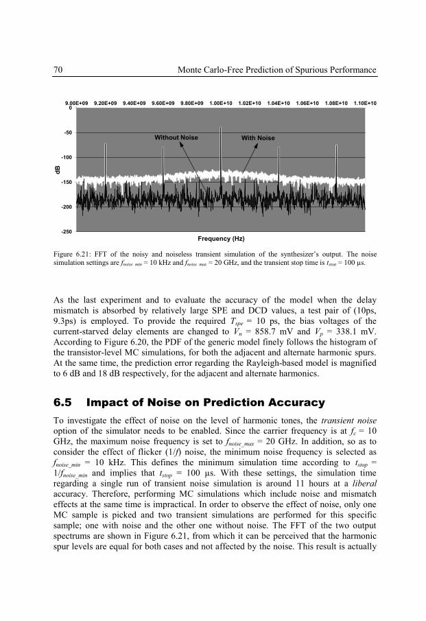
70 Monte Carlo-Free Prediction of Spurious Performance
As the last experiment and to evaluate the accuracy of the model when the delay
mismatch is absorbed by relatively large SPE and DCD values, a test pair of (10ps,
9.3ps) is employed. To provide the required Tspe = 10 ps, the bias voltages of the
current-starved delay elements are changed to Vn = 858.7 mV and Vp = 338.1 mV.
According to Figure 6.20, the PDF of the generic model finely follows the histogram of
the transistor-level MC simulations, for both the adjacent and alternate harmonic spurs.
At the same time, the prediction error regarding the Rayleigh-based model is magnified
to 6 dB and 18 dB respectively, for the adjacent and alternate harmonics.
6.5 Impact of Noise on Prediction Accuracy
To investigate the effect of noise on the level of harmonic tones, the transient noise
option of the simulator needs to be enabled. Since the carrier frequency is at fc = 10
GHz, the maximum noise frequency is set to fnoise_max = 20 GHz. In addition, so as to
consider the effect of flicker (1/f) noise, the minimum noise frequency is selected as
fnoise_min = 10 kHz. This defines the minimum simulation time according to tstop =
1/fnoise_min and implies that tstop = 100 µs. With these settings, the simulation time
regarding a single run of transient noise simulation is around 11 hours at a liberal
accuracy. Therefore, performing MC simulations which include noise and mismatch
effects at the same time is impractical. In order to observe the effect of noise, only one
MC sample is picked and two transient simulations are performed for this specific
sample; one with noise and the other one without noise. The FFT of the two output
spectrums are shown in Figure 6.21, from which it can be perceived that the harmonic
spur levels are equal for both cases and not affected by the noise. This result is actually
-250
-200
-150
-100
-50
09.00E+09 9.20E+09 9.40E+09 9.60E+09 9.80E+09 1.00E+10 1.02E+10 1.04E+10 1.06E+10 1.08E+10 1.10E+10
With NoiseWithout Noise
Frequency (Hz)
dB
Figure 6.21: FFT of the noisy and noiseless transient simulation of the synthesizer’s output. The noise
simulation settings are fnoise_min = 10 kHz and fnoise_max = 20 GHz, and the transient stop time is tstop = 100 µs.
6.6 Summary 71
expected. The random timing uncertainty on the DLL output phases (caused by the
noise) differs from cycle to cycle and does not exhibit any periodicity. Therefore, it
affects the phase noise rather than the sideband spurs of the synthesizer. Accordingly, it
can be concluded that the accuracy of the introduced prediction model will not be
degraded by the circuit noise.
6.6 Summary
Based on the derived closed-form expressions for the PDF and mean value of the spur
magnitudes, a prediction model for characterizing the spurious performance of edge-
combining DLL-based synthesizers is introduced. The important characteristic of the
model is that its prediction accuracy is independent of the design parameters and the
practical values of the system non-idealities in the context of frequency synthesis for
wireless applications. Hence, the model is comparable to MC method in terms of
accuracy and robustness, whereas it alleviates the need for exhaustive statistical
simulations. The accuracy of the model is investigated through MC simulations of the
behavioral model of the synthesizer, against wide-range values of SPE, DCD, and delay
SD. Moreover, validity of the model is further inspected by performing MC simulations
on a transistor-level model of the synthesizer, which is designed in a standard 65-nm
CMOS process. Comparison of the simulated and the calculated results verifies the
accuracy of the method, and also that the prediction model is generic and can be
considered as a reliable replacement to MC method for characterizing the spurious
performance of DLL-based frequency synthesizers. Finally, the effect of noise on the
level of harmonic spurs was inspected. It was demonstrated that since noise results in
random jitter, it does not generate any periodicity on the DLL output edges, and hence,
does not affect the spurious performance. This implies that the accuracy of the
prediction model is not degraded by the circuit noise.

72 Monte Carlo-Free Prediction of Spurious Performance
73
Chapter 7
Spur-Aware Design Flow
7.1 Introduction
Based on closed-form expressions, a prediction model for spurious performance of
edge-combining DLL-based synthesizers was developed in Chapter 6. In this chapter,
which is mainly based on [1], [2], the introduced prediction model is utilized to develop
a spur-aware design flow for DLL-based synthesizers, in order to accelerate their
iterative design procedure. Employing this design flow and without MC simulations, the
required stage-delay SD that satisfies a certain SCR requirement, can be accurately
predicted. Based on the calculated delay SD, the corresponding delay stage circuitry can
be accordingly designed.
Section 7.2 discusses the standard mismatch-aware design flow. In Section 7.3 the
“accelerated” spur-aware synthesizer design flow is introduced which is utilized in the
design example of Section 7.4 to find the required stage-delay SD which satisfies the
spurious performance of WiMedia UWB standard. Finally, the chapter is summarized in
Section 7.5.
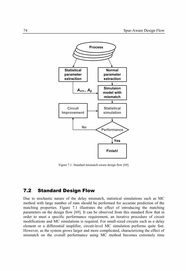
74 Spur-Aware Design Flow
7.2 Standard Design Flow
Due to stochastic nature of the delay mismatch, statistical simulations such as MC
method with large number of runs should be performed for accurate prediction of the
matching properties. Figure 7.1 illustrates the effect of introducing the matching
parameters on the design flow [69]. It can be observed from this standard flow that in
order to meet a specific performance requirement, an iterative procedure of circuit
modifications and MC simulations is required. For small-sized circuits such as a delay
element or a differential amplifier, circuit-level MC simulation performs quite fast.
However, as the system grows larger and more complicated, characterizing the effect of
mismatch on the overall performance using MC method becomes extremely time
Process
Normal
parameter
extraction
Simulaion
model with
mismatch
Statistical
simulation
Statistical
parameter
extraction
Circuit
Improvement
PerformanceNo
AVTH , Aβ
Finish!
Yes
Figure 7.1: Standard mismatch-aware design flow [69].
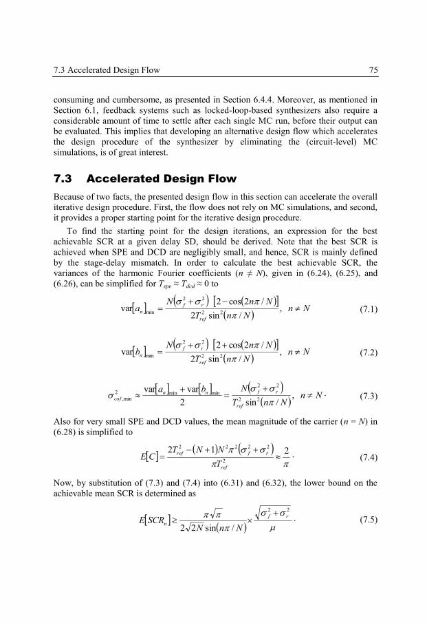
7.3 Accelerated Design Flow 75
consuming and cumbersome, as presented in Section 6.4.4. Moreover, as mentioned in
Section 6.1, feedback systems such as locked-loop-based synthesizers also require a
considerable amount of time to settle after each single MC run, before their output can
be evaluated. This implies that developing an alternative design flow which accelerates
the design procedure of the synthesizer by eliminating the (circuit-level) MC
simulations, is of great interest.
7.3 Accelerated Design Flow
Because of two facts, the presented design flow in this section can accelerate the overall
iterative design procedure. First, the flow does not rely on MC simulations, and second,
it provides a proper starting point for the iterative design procedure.
To find the starting point for the design iterations, an expression for the best
achievable SCR at a given delay SD, should be derived. Note that the best SCR is
achieved when SPE and DCD are negligibly small, and hence, SCR is mainly defined
by the stage-delay mismatch. In order to calculate the best achievable SCR, the
variances of the harmonic Fourier coefficients (n ≠ N), given in (6.24), (6.25), and
(6.26), can be simplified for Tspe ≈ Tdcd ≈ 0 to
Nn
NnT
NnNa
ref
rf
n
,/sin2
/2cos2var
22
22
min
(7.1)
Nn
NnT
NnNb
ref
rf
n
,/sin2
/2cos2var
22
22
min
(7.2)
NnNnT
Nba
ref
rfnn
cof
,/sin2
varvar22
22
minmin2
min,
. (7.3)
Also for very small SPE and DCD values, the mean magnitude of the carrier (n = N) in
(6.28) is simplified to
2122
22222
ref
rfref
T
NNTCE . (7.4)
Now, by substitution of (7.3) and (7.4) into (6.31) and (6.32), the lower bound on the
achievable mean SCR is determined as
22
/sin22
rf
nNnN
SCRE
. (7.5)
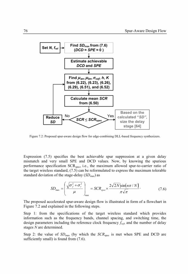
76 Spur-Aware Design Flow
Expression (7.5) specifies the best achievable spur suppression at a given delay
mismatch and very small SPE and DCD values. Now, by knowing the spurious
performance specification SCRspec, i.e., the maximum allowed spur-to-carrier ratio of
the target wireless standard, (7.5) can be reformulated to express the maximum tolerable
standard deviation of the stage-delay (SDmax) as
NnNSCRSD spec
rf /sin22
max
22
max
. (7.6)
The proposed accelerated spur-aware design flow is illustrated in form of a flowchart in
Figure 7.2 and explained in the following steps.
Step 1: from the specifications of the target wireless standard which provides
information such as the frequency bands, channel spacing, and switching time, the
design parameters including the reference clock frequency fref, and the number of delay
stages N are determined.
Step 2: the value of SDmax (by which the SCRspec is met when SPE and DCD are
sufficiently small) is found from (7.6).
Find SDmax from (7.6)
(DCD ≈ SPE ≈ 0 )
Estimate achievable
DCD and SPE
SCR ≤ SCRspec
Yes
Calculate mean SCR
from (6.50)
Find μan, μbn, σcof, h, K
from (6.22), (6.23), (6.26),
(6.29), (6.51), and (6.52)
Reduce
SD
Based on the
calculated “SD”,
size the delay
stage [64]
Set N, fref
No
Figure 7.2: Proposed spur-aware design flow for edge-combining DLL-based frequency synthesizers.
7.4 WiMedia UWB Synthesizer; a Design Example 77
Step 3: the achievable values of SPE and DCD are estimated based on the architectural
and circuit techniques which are utilized to design the synthesizer.
Step 4: the initially-calculated SDmax and the estimated SPE and DCD values are
employed to calculate E[an], E[bn], σcof, E[C], h΄ and K΄ respectively from (6.22), (6.23),
(6.26), (6.29), (6.51), and (6.52).
Step 5: the provided mean SCR is determined from (6.50).
Step 6: if the mean SCR is larger than SCRspec, then the delay SD is reduced and the new
mean SCR is calculated from Step 4 and 5. This procedure is repeated until E[SCR] ≤
SCRspec.
Step 7: The calculated value of the delay SD is utilized to perform the sizing and
biasing of the delay stage transistors using a similar approach as in [64].
7.4 WiMedia UWB Synthesizer; a Design Example
In this section, the introduced design flow is employed to find the required stage-delay
SD for a DLL-based frequency synthesizer, which is supposed to satisfy the spurious
performance requirement of WiMedia UWB bandgroup 1.
7.4.1 Design Procedure
The spectrum allocation of WiMedia UWB and the coexisting wireless technologies
were illustrated in Figure 3.1. Also the corresponding spur suppression requirements
were discussed in Section 3.2.2. Accordingly, due to the strong out-of-band interferers
from IEEE 802.11 a/b/g, those spurious tones which fall within 2.4 ‒ 5 GHz range,
should be below ‒45 dBc. Note that the SCR provided by the DLL-based synthesizer
can be relaxed by a few dBs depending on the EC type. An EC with LC-tank load [36]
is utilized which filters the harmonic spurs to some extent, depending on its Q factor. In
addition, utilizing as twice as the required input frequency and performing frequency
division to generate quadrature carriers, will also suppress the spur levels. Therefore, it
is assumed that a 6-dB suppression is already provided, implying that SCRspec of ‒39
dBc should be delivered. Shown in Figure 3.1, WiMedia bandgroup 1 consists of three
sub-bands with center frequencies at 264 × 13, 264 × 15, and 264 × 17 MHz,
respectively. Hence, following Step 1, the number of delay stages is N = 17 and a
reference clock of fref = 2 × 264 MHz is utilized. Now from Step 2, SDmax is calculated
using (7.6) to provide SCRspec = ‒39 dBc for the adjacent harmonic spur (n = 16). Thus,
%43.017/16sin342
10)( 20
39
max
22
rf . (7.7)
To accomplish Step 3, it is assumed that DCD and SPE values of Tdcd = 0.1 µ ≈ 11 ps
and Tspe = 0.02 µ ≈ 2 ps can be achieved.
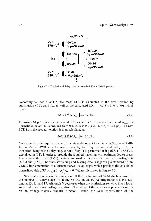
78 Spur-Aware Design Flow
According to Step 4 and 5, the mean SCR is calculated in the first iteration by
substitution of Tdcd and Tspe as well as the calculated SDmax = 0.43% into (6.50), which
gives
dBc 38log20 1,16 SCRE . (7.8)
Following Step 6, since the calculated SCR value in (7.8) is larger than the SCRspec, the
normalized delay SD is reduced from 0.43% to 0.4% (e.g., σr = σf = 0.31 ps). The new
SCR from the second iteration is then calculated as
dBc 93log20 2,16 SCRE . (7.9)
Consequently, the required value of the stage-delay SD to achieve SCRspec = ‒39 dBc
for WiMedia UWB is determined. Now by knowing the required delay SD, the
transistor sizing of the delay stage circuit (Step 7) is performed using (6.53) ‒ (6.55), as
explained in [64]. In order to provide the required matching with optimum device areas,
low voltage threshold (LVT) devices are used to increase the overdrive voltages in
(6.53) and (6.54). The transistor sizing and biasing details regarding a standard 65-nm
CMOS implementation of a current-starved delay stage, which provides the calculated
normalized delay SD of 22
rf = 0.4%, are illustrated in Figure 7.3.
Note that to synthesize the carriers of all three sub-bands of WiMedia bandgroup 1,
the number of delay stages N in the VCDL should be reconfigurable [3], [6], [35]
among 13, 15, and 17. Although N decreases when the synthesizer switches into a lower
sub-band, the control voltage also drops. The value of the voltage-drop depends on the
VCDL voltage-to-delay transfer function. Hence, the SCR specification of the
Vp =
370mV
in out
60/0.8
Vth=-322mV
Vn =
810mV
15/0.2415/0.24
Vth=-362mV
5/0.24
Vth=358mV5/0.24
20/0.8
Vth=298mV
VDD=1.2 V
Figure 7.3: The designed delay stage in a standard 65-nm CMOS process.
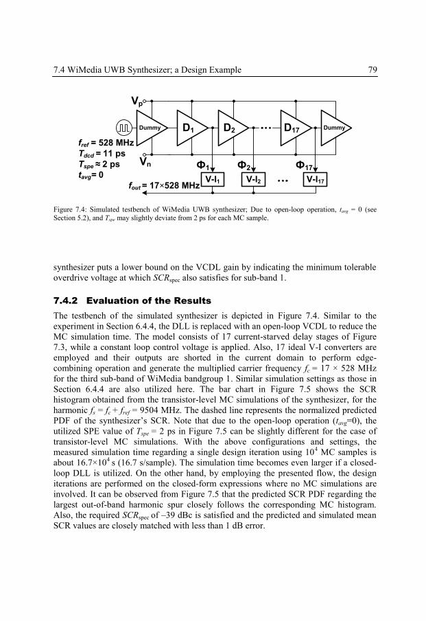
7.4 WiMedia UWB Synthesizer; a Design Example 79
synthesizer puts a lower bound on the VCDL gain by indicating the minimum tolerable
overdrive voltage at which SCRspec also satisfies for sub-band 1.
7.4.2 Evaluation of the Results
The testbench of the simulated synthesizer is depicted in Figure 7.4. Similar to the
experiment in Section 6.4.4, the DLL is replaced with an open-loop VCDL to reduce the
MC simulation time. The model consists of 17 current-starved delay stages of Figure
7.3, while a constant loop control voltage is applied. Also, 17 ideal V-I converters are
employed and their outputs are shorted in the current domain to perform edge-
combining operation and generate the multiplied carrier frequency fc = 17 × 528 MHz
for the third sub-band of WiMedia bandgroup 1. Similar simulation settings as those in
Section 6.4.4 are also utilized here. The bar chart in Figure 7.5 shows the SCR
histogram obtained from the transistor-level MC simulations of the synthesizer, for the
harmonic fs = fc + fref = 9504 MHz. The dashed line represents the normalized predicted
PDF of the synthesizer’s SCR. Note that due to the open-loop operation (tavg=0), the
utilized SPE value of Tspe = 2 ps in Figure 7.5 can be slightly different for the case of
transistor-level MC simulations. With the above configurations and settings, the
measured simulation time regarding a single design iteration using 104 MC samples is
about 16.7×10⁴
s (16.7 s/sample). The simulation time becomes even larger if a closed-
loop DLL is utilized. On the other hand, by employing the presented flow, the design
iterations are performed on the closed-form expressions where no MC simulations are
involved. It can be observed from Figure 7.5 that the predicted SCR PDF regarding the
largest out-of-band harmonic spur closely follows the corresponding MC histogram.
Also, the required SCRspec of ‒39 dBc is satisfied and the predicted and simulated mean
SCR values are closely matched with less than 1 dB error.
Dummy D1 D17 Dummy
Ф1 Ф17
V-I17V-I1
D2
Ф2
V-I2
Vp
Vn
fref = 528 MHz
Tdcd = 11 ps
Tspe ≈ 2 ps
tavg= 0
fout = 17×528 MHz
Figure 7.4: Simulated testbench of WiMedia UWB synthesizer; Due to open-loop operation, tavg = 0 (see
Section 5.2), and Tspe may slightly deviate from 2 ps for each MC sample.
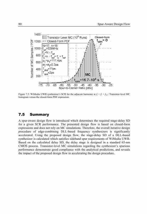
80 Spur-Aware Design Flow
7.5 Summary
A spur-aware design flow is introduced which determines the required stage-delay SD
for a given SCR performance. The presented design flow is based on closed-form
expressions and does not rely on MC simulations. Therefore, the overall iterative design
procedure of edge-combining DLL-based frequency synthesizers is significantly
accelerated. Using the proposed design flow, the stage-delay SD of a DLL-based
synthesizer is calculated which satisfies sideband spur requirements of WiMedia UWB.
Based on the calculated delay SD, the delay stage is designed in a standard 65-nm
CMOS process. Transistor-level MC simulations regarding the synthesizer’s spurious
performance demonstrate good compliance with the analytical predictions, and reveals
the impact of the proposed design flow in accelerating the design procedure.
Figure 7.5: WiMedia UWB synthesizer’s SCR for the adjacent harmonic at fs = fc + fref : Transistor-level MC
histogram versus the closed-form PDF expression.
81
Chapter 8
An Injection-Locked DLL-Based
UWB Synthesizer
8.1 Introduction
This chapter covers [3]‒[6] and presents the development, design, and implementation
of a new architecture for fast hopping DLL-based frequency synthesis for WiMedia
UWB bandgroup1. To achieve fast channel switching, an open-loop phase
compensation scheme is introduced. The DLL employs a variable-gain and variable-
stage VCDL to compensate the generated phase error due to band switching.
Furthermore, the fast settling characteristic of the loop facilities the use of an injection-
locked oscillator at synthesizer’s output (which utilizes the remaining time slot for its
own settling), to minimize the current consumption in the EC circuitry. In addition, two
calibration techniques are introduced to make the presented compensation technique
immune to PVT variations.
Section 8.2 introduces the proposed synthesizer architecture. The corresponding
design considerations are discussed in Section 8.3. In Section 8.4, the design of
synthesizer’s building blocks and the calibration techniques are presented in details. The
experimental results of the implemented synthesizer in a 65-nm CMOS process is
demonstrated in Section 8.5, followed by a summary in Section 8.6.
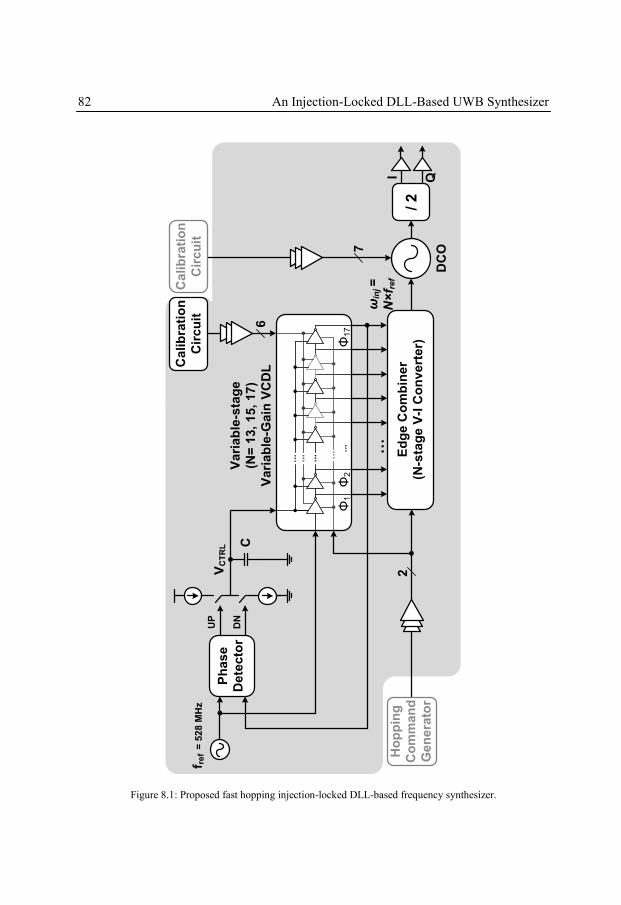
82 An Injection-Locked DLL-Based UWB Synthesizer
Ph
ase
Dete
cto
r
f ref
= 5
28 M
Hz
C
UP
DN
VC
TR
L
Vari
ab
le-s
tag
e
(N=
13, 15, 17
)
Vari
ab
le-G
ain
VC
DL
Ed
ge C
om
bin
er
(N-s
tag
e V
-I C
on
vert
er)
Calib
rati
on
Cir
cu
it
DC
O
/ 2
Calib
rati
on
Cir
cu
it
6
7
2I Q
Ho
pp
ing
Co
mm
an
d
Gen
era
tor
ωin
j =
N×
f ref
Φ17
Φ2
Φ1
Figure 8.1: Proposed fast hopping injection-locked DLL-based frequency synthesizer.
8.2 Architecture 83
8.2 Architecture
The functionality of an edge-combining DLL-based frequency multiplier has been
explained in Section 4.2. Figure 8.1 demonstrates the proposed architecture of the fast
hopping injection-locked synthesizer which targets WiMedia UWB communication in
bandgroup 1. The synthesizer consists of a CP DLL that is locked to a 528-MHz
reference clock, and according to the number of delay elements in the VCDL (N=13,
15, 17), it generates equally-spaced output phases. The DLL phases are then converted
into currents through V-I converters in the EC. The currents are then shorted together to
generate the multiplied frequency. The final output current of the EC acts as an injection
signal to a cross-coupled LC oscillator, forming an ILO structure. Under certain
conditions (which is when the injection signal frequency is within the lock range of the
oscillator), the oscillator stops oscillating at its free-running frequency and locks to the
frequency of the low-amplitude injection signal. Therefore, the current consumption of
the N-stage V-I converter is minimized without losing the output swing. In order to
avoid transmitter (TX) frequency pulling, the system synthesizes frequencies at twice
the carriers of bandgroup 1. A static current-mode logic (CML) divide-by-2 circuit is
employed to generate the desired frequencies. The frequency division also provides
quadrature clocks and enables the synthesizer to be utilized in direct conversion
transmitters and zero-IF receivers.
The novelty of the proposed architecture is explained as follows. In order to
synthesize different carrier frequencies, the VCDL should exhibit variable-stage
characteristic. This has been achieved in the conventional approach through
multiplexing different output phases of the DLL as the feedback signal to the PD [35].
This approach requires a dedicated pair of PD/CP for each sub-band so as to avoid the
generation of glitches. This results in additional power consumption. In the presented
architecture, a bypass mechanism is employed to enable/disable the delay elements
from the delay chain, while the load symmetry is preserved. Therefore, the feedback is
always taken from the VCDL output and the need for the extra MUX and PD/CP pairs
are alleviated. Another characteristic of the conventional DLL-based synthesizer is that
it relies on relatively wide bandwidth of the DLL to achieve fast settling. Although a
wideband DLL is theoretically stable due to its fist-order loop, an extremely large
bandwidth can still cause stability issues in practice [77]. Also, a large loop bandwidth
requires a smaller loop capacitance. This leads to larger ripples on the loop control
voltage, giving rise to the level of sideband spurs at the output spectrum of the
synthesizer. In this architecture, certain mechanism is utilized, through which a
compensation phase is injected to the loop at the time of band switching. As a result, the
change in the VCDL delay-length due to band switching is compensated in an open-
loop regime to achieve fast hopping even at a small bandwidth. The third technique is
the use of injection-locking to minimize the power dissipation in the multistage V-I
converter of the EC. The negative-resistance oscillator is locked to the low-current
injection signal from the EC and produces a high swing at the synthesizer output. The
fast switching DLL scheme leaves enough time margins for the ILO settling.
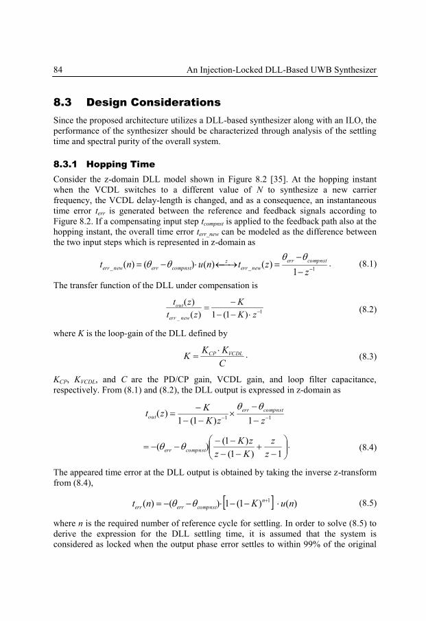
84 An Injection-Locked DLL-Based UWB Synthesizer
8.3 Design Considerations
Since the proposed architecture utilizes a DLL-based synthesizer along with an ILO, the
performance of the synthesizer should be characterized through analysis of the settling
time and spectral purity of the overall system.
8.3.1 Hopping Time
Consider the z-domain DLL model shown in Figure 8.2 [35]. At the hopping instant
when the VCDL switches to a different value of N to synthesize a new carrier
frequency, the VCDL delay-length is changed, and as a consequence, an instantaneous
time error terr is generated between the reference and feedback signals according to
Figure 8.2. If a compensating input step tcompnst is applied to the feedback path also at the
hopping instant, the overall time error terr_new can be modeled as the difference between
the two input steps which is represented in z-domain as
1__
1)()()()(
zztnunt
compnsterr
newerr
z
compnsterrnewerr
. (8.1)
The transfer function of the DLL under compensation is
1
_ )1(1)(
)(
zK
K
zt
zt
newerr
out (8.2)
where K is the loop-gain of the DLL defined by
C
KKK VCDLCP . (8.3)
KCP, KVCDL, and C are the PD/CP gain, VCDL gain, and loop filter capacitance,
respectively. From (8.1) and (8.2), the DLL output is expressed in z-domain as
11 1)1(1)(
zzK
Kzt
compnsterr
out
1)1(
)1()(
z
z
Kz
zKcompnsterr . (8.4)
The appeared time error at the DLL output is obtained by taking the inverse z-transform
from (8.4),
)()1(1)()( 1 nuKnt n
compnsterrerr (8.5)
where n is the required number of reference cycle for settling. In order to solve (8.5) to
derive the expression for the DLL settling time, it is assumed that the system is
considered as locked when the output phase error settles to within 99% of the original
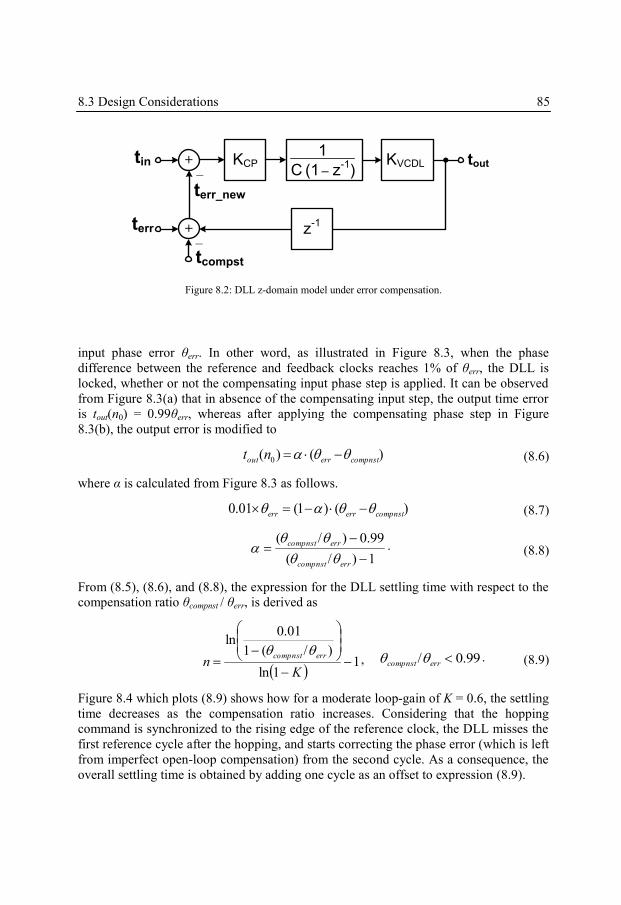
8.3 Design Considerations 85
input phase error θerr. In other word, as illustrated in Figure 8.3, when the phase
difference between the reference and feedback clocks reaches 1% of θerr, the DLL is
locked, whether or not the compensating input phase step is applied. It can be observed
from Figure 8.3(a) that in absence of the compensating input step, the output time error
is tout(n0) = 0.99θerr, whereas after applying the compensating phase step in Figure
8.3(b), the output error is modified to
)()( 0 compnsterrout nt (8.6)
where α is calculated from Figure 8.3 as follows.
)()1(01.0 compnsterrerr (8.7)
1)/(
99.0)/(
errcompnst
errcompnst
. (8.8)
From (8.5), (8.6), and (8.8), the expression for the DLL settling time with respect to the
compensation ratio θcompnst / θerr, is derived as
1
1ln
)/(1
01.0ln
Kn
errcompnst ,
99.0/ errcompnst .
(8.9)
Figure 8.4 which plots (8.9) shows how for a moderate loop-gain of K = 0.6, the settling
time decreases as the compensation ratio increases. Considering that the hopping
command is synchronized to the rising edge of the reference clock, the DLL misses the
first reference cycle after the hopping, and starts correcting the phase error (which is left
from imperfect open-loop compensation) from the second cycle. As a consequence, the
overall settling time is obtained by adding one cycle as an offset to expression (8.9).
+ KCP KVCDL1
C (1 z-1
)
z-1
+terr
tcompst
_tin tout
terr_new
–
–
Figure 8.2: DLL z-domain model under error compensation.
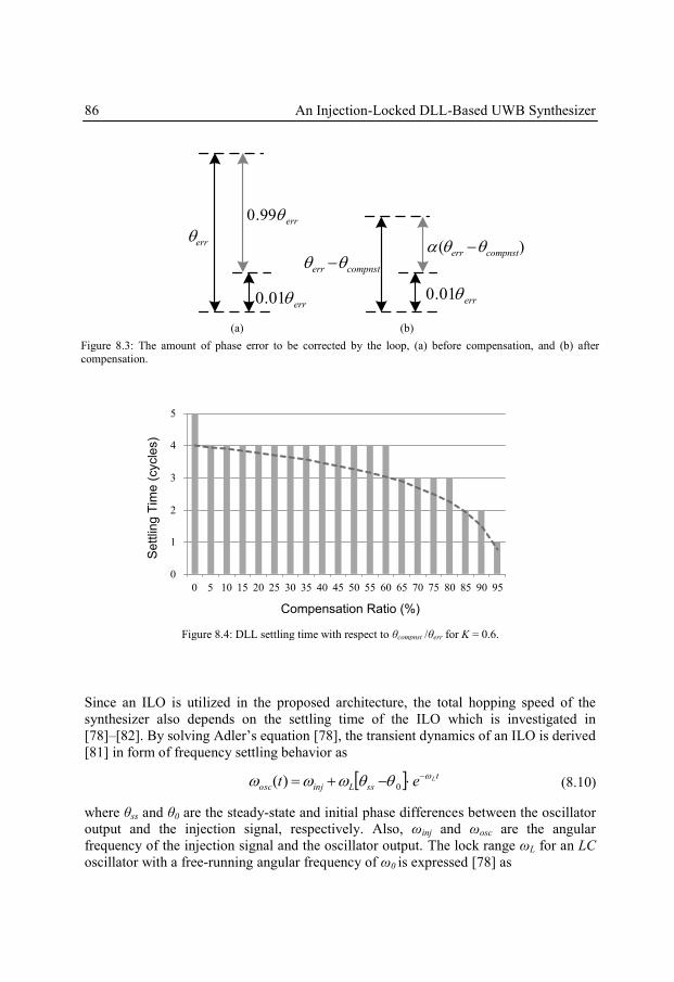
86 An Injection-Locked DLL-Based UWB Synthesizer
Since an ILO is utilized in the proposed architecture, the total hopping speed of the
synthesizer also depends on the settling time of the ILO which is investigated in
[78]‒[82]. By solving Adler’s equation [78], the transient dynamics of an ILO is derived
[81] in form of frequency settling behavior as
t
ssLinjoscLet
0)(
(8.10)
where θss and θ0 are the steady-state and initial phase differences between the oscillator
output and the injection signal, respectively. Also, ωinj and ωosc are the angular
frequency of the injection signal and the oscillator output. The lock range ωL for an LC
oscillator with a free-running angular frequency of ω0 is expressed [78] as
err
compnsterr
err01.0 err01.0
err99.0
)( compnsterr
(a) (b)
Figure 8.3: The amount of phase error to be corrected by the loop, (a) before compensation, and (b) after
compensation.
0
1
2
3
4
5
1 2 3 4 5 6 7 8 9 10 11 12 13 14 15 16 17 18 19 20
0
1
2
3
4
5
0 5 10 15 20 25 30 35 40 45 50 55 60 65 70 75 80 85 90 95
Compensation Ratio (%)
Settlin
g T
ime (
cycle
s)
Figure 8.4: DLL settling time with respect to θcompnst /θerr for K = 0.6.
8.3 Design Considerations 87
osc
inj
LI
I
Q
2
0
(8.11)
where Iinj and Iosc are the injection and oscillation amplitudes respectively, and Q is the
quality factor of the tank. It is observed from (8.10) that fast lock time can be achieved
by two means; increasing the lock range and/or closely matching the steady-state phase
conditions for each of the hopping cases [13]. Note that there exists a lower bound on
settling time of an ILO, and that is the time constant of the LC-tank (defined by its
bandwidth) to respond to a change in its resonant frequency [26].
8.3.2 Phase Noise and Harmonic Spurs
In a DLL-based synthesizer, the timing uncertainties on the delay edges are
accumulated within only one reference cycle and reset back to zero at the next rising
edge of the reference clock. This results in a flat phase noise spectrum which only
contains two slope regions; the flicker noise (1/f) and the thermal noise [35], [36].
Therefore, the total phase noise of a DLL-based frequency multiplier is mainly defined
by the noise of its input clock and input buffers, as well as the accumulated jitter within
one reference cycle in its delay line. The phase noise performance of an ILO is
investigated in [79], [82]. For injection frequencies close to the free-running frequency
of the LC oscillator (ωinj ≈ ω0), the total phase noise of the ILO is dominated by the
phase noise of the injection signal, whereas when the injection frequency gets close to
the edges of the lock range (|ωinj ‒ ω0| ≈ ωL), the phase noise of the free-running
oscillator dominates. As a conclusion, by providing a low phase noise injection signal
from the DLL-based frequency multiplier, as well as by designing the resonant
frequency of the LC-tank close to the injection frequency, the total close-in phase noise
(within the lock range) of the synthesizer can be reduced. However, due to process
variations and the inaccuracies of the models, it is not easy to design an accurate free-
running frequency [79]. Therefore, to keep the resonant frequency away from the edges
of the lock range, a tunable resonant frequency with relatively high frequency resolution
should be employed using a digitally-controlled capacitor bank.
The spurious tones in an ILO are originated from the harmonic contents of the
injection signal. In sub-harmonic injection-locking, the spurious performance is poor
due to the rich harmonic contents of the original injected signal (which is a low
frequency square wave clock), unless pulse shaping techniques and filtering are
employed [13], [26], [27]. In fundamental-tone injection-locking which the proposed
architecture is based on, the oscillator is locked to the fundamental component of the
injection signal. In the proposed architecture, the fundamental signal is generated by the
DLL-based frequency multiplier. Therefore, the overall sideband spur levels depend on
the harmonic tones in the edge-combining DLL-based multiplier, which are defined by
the SPE, DCD, and stage-delay mismatch. This topic has been studied in details in
Chapters 5 ‒ 7.
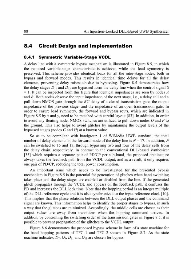
88 An Injection-Locked DLL-Based UWB Synthesizer
8.4 Circuit Design and Implementation
8.4.1 Symmetric Variable-Stage VCDL
A delay line with a symmetric bypass mechanism is illustrated in Figure 8.5, in which
the required variable-stage characteristic is achieved while the load symmetry is
preserved. This scheme provides identical loads for all the inter-stage nodes, both in
bypass and forward modes. This results in identical time delays for all the delay
elements, preventing delay mismatch due to bypassing. Figure 8.5 demonstrates how
the delay stages D11 and D13 are bypassed form the delay line when the control signal S
= 1. It can be inspected from this figure that identical impedances are seen by nodes A
and B. Both nodes observe the input impedance of the next stage, i.e., a delay cell and a
pull-down NMOS gate through the RC-delay of a closed transmission gate, the output
impedance of the previous stage, and the impedance of an open transmission gate. In
order to ensure load symmetry, the forward and bypass routs, which are indicated in
Figure 8.5 by x and y, need to be matched with careful layout [83]. In addition, in order
to avoid any floating node, NMOS switches are utilized to pull down nodes D and F to
the ground. This also helps to avoid glitches by maintaining the output levels of the
bypassed stages (nodes G and H) at a known value.
So as to be compliant with bandgroup 1 of WiMedia UWB standard, the total
number of delay elements in the forward mode of the delay line is N = 17. In addition, N
can be switched to 15 and 13, through bypassing two and four of the delay cells from
the delay chain, respectively. In contrast to the conventional DLL-based synthesizer
[35] which requires a separate pair of PD/CP per sub-band, the proposed architecture
always takes the feedback path from the VCDL output, and as a result, it only requires
one pair of PD/CP, reducing the total power consumption.
An important issue which needs to be investigated for the presented bypass
mechanism in Figure 8.5 is the potential for generation of glitches when band switching
takes place and the delay stages are enabled or disabled from the line. If the generated
glitch propagates through the VCDL and appears on the feedback path, it confuses the
PD and increases the DLL lock time. Note that the hopping period is an integer multiple
of the DLL reference cycle and it is also synchronized to the input reference clock [10].
This implies that the phase relations between the DLL output phases and the command
signal are known. This information helps to identify the proper stages to bypass, in such
a way that the glitches are minimized. Accordingly, the middle cells are chosen as their
output values are away from transitions when the hopping command arrives. In
addition, by controlling the switching order of the transmission gates in Figure 8.5, it is
possible to prevent propagation of the glitches to the VCDL output.
Figure 8.6 demonstrates the proposed bypass scheme in form of a state machine for
the band hopping patterns of TFC 1 and TFC 2 shown in Figure 8.7. As the state
machine indicates, D7, D9, D11 and D13 are chosen for bypass.
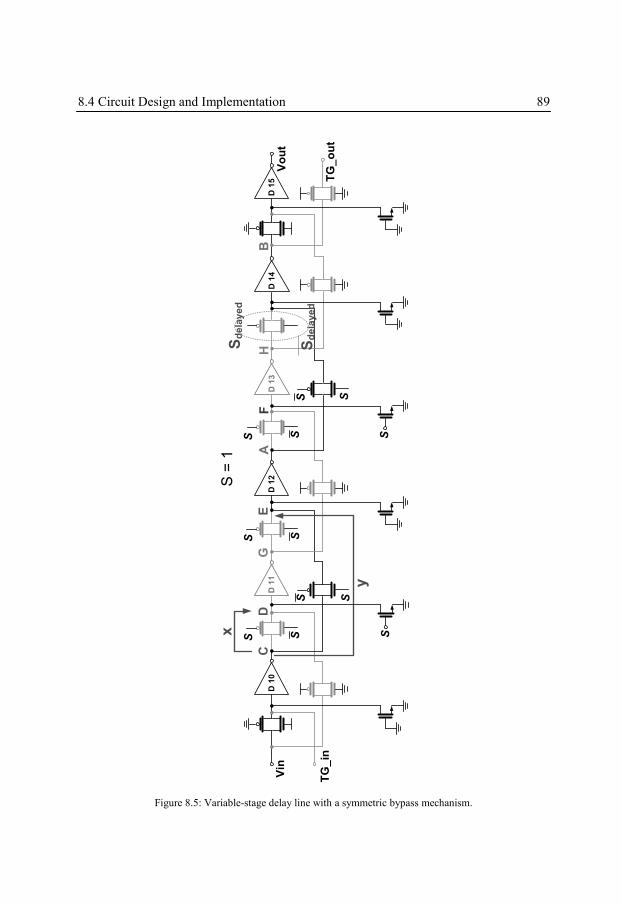
8.4 Circuit Design and Implementation 89
Vin
TG
_in
Vo
ut
TG
_o
ut
D 1
0D
11
D 1
2D
13
D 1
4
SS
S
SS
S =
1
S
S SS S
D 1
5A
BC
DE
x
y
F
SS
Sd
ela
yed
Sd
ela
yed
GH
Figure 8.5: Variable-stage delay line with a symmetric bypass mechanism.
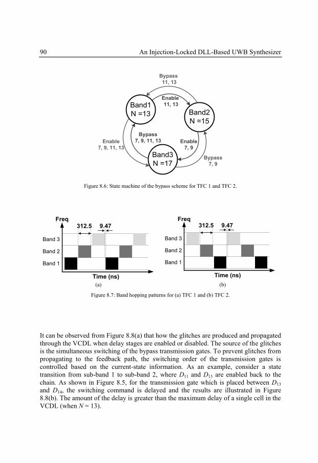
90 An Injection-Locked DLL-Based UWB Synthesizer
It can be observed from Figure 8.8(a) that how the glitches are produced and propagated
through the VCDL when delay stages are enabled or disabled. The source of the glitches
is the simultaneous switching of the bypass transmission gates. To prevent glitches from
propagating to the feedback path, the switching order of the transmission gates is
controlled based on the current-state information. As an example, consider a state
transition from sub-band 1 to sub-band 2, where D11 and D13 are enabled back to the
chain. As shown in Figure 8.5, for the transmission gate which is placed between D13
and D14, the switching command is delayed and the results are illustrated in Figure
8.8(b). The amount of the delay is greater than the maximum delay of a single cell in the
VCDL (when N = 13).
Enable
7, 9
Bypass
7, 9, 11, 13
Band1
N =13
Band3
N =17
Band2
N =15
Enable
11, 13
Enable
7, 9, 11, 13
Bypass
11, 13
Bypass
7, 9
Figure 8.6: State machine of the bypass scheme for TFC 1 and TFC 2.
Band 1
Band 2
Band 3
Freq
Time (ns)
9.47312.5
Band 1
Band 2
Band 3
Freq
Time (ns)
9.47312.5
(a) (b)
Figure 8.7: Band hopping patterns for (a) TFC 1 and (b) TFC 2.
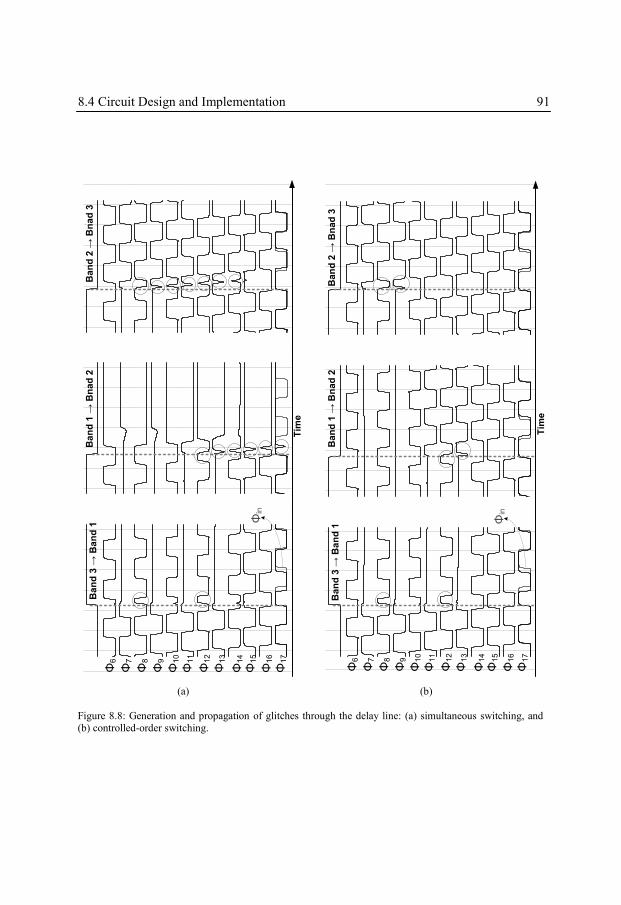
8.4 Circuit Design and Implementation 91
Tim
e
Ban
d 1
→ B
nad
2B
an
d 3
→ B
an
d 1
Ban
d 2
→ B
nad
3
Φ6
Φ7
Φ8
Φ9
Φ10
Φ11
Φ12
Φ13
Φ14
Φ15
Φ16
Φ17
Φin
Tim
e
Ba
nd
1 →
Bn
ad
2B
an
d 3
→ B
an
d 1
Ba
nd
2 →
Bn
ad
3
Φin
Φ6
Φ7
Φ8
Φ9
Φ1
0
Φ1
1
Φ1
2
Φ1
3
Φ1
4
Φ1
5
Φ1
6
Φ1
7
(a) (b)
Figure 8.8: Generation and propagation of glitches through the delay line: (a) simultaneous switching, and (b) controlled-order switching.
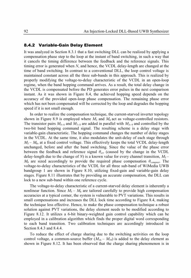
92 An Injection-Locked DLL-Based UWB Synthesizer
8.4.2 Variable-Gain Delay Element
It was analyzed in Section 8.3.1 that a fast switching DLL can be realized by applying a
compensation phase step to the loop at the instant of band switching, in such a way that
it cancels the timing difference between the feedback and the reference signals. This
timing error is generated when N, and hence, the VCDL delay-length are changed at the
time of band switching. In contrast to a conventional DLL, the loop control voltage is
maintained constant across all the three sub-bands in this approach. This is realized by
properly modifying the voltage-to-delay characteristic of the VCDL in an open-loop
regime, when the band hopping command arrives. As a result, the total delay change in
the VCDL is compensated before the PD generates error pulses in the next comparison
instant. As it was shown in Figure 8.4, the achieved hopping speed depends on the
accuracy of the provided open-loop phase compensation. The remaining phase error
which has not been compensated will be corrected by the loop and degrades the hopping
speed if it is not small enough.
In order to realize the compensation technique, the current-starved inverter topology
shown in Figure 8.9 is employed where M3 and M4 act as voltage-controlled resistors.
The transistor pairs M5, 6 and M7, 8 are added in parallel with M3, 4 and controlled by the
two-bit band hopping command signal. The resulting scheme is a delay stage with
variable-gain characteristic. The hopping command changes the number of delay stages
in the VCDL. At the same time, it also modulates the unit-delay of each stage through
M5 ‒ M8, at a fixed control voltage. This effectively keeps the total VCDL delay-length
unchanged, before and after the band switching. Since the value of the phase error
between the feedback and reference signal θerr (caused by the change in the VCDL
delay-length due to the change of N) is a known value for every channel transition, M5 ‒
M8 are sized accordingly to provide the required phase compensation θcompnst. The
voltage-to-delay characteristics of the VCDL for all three sub-band of WiMedia UWB
bandgroup 1 are shown in Figure 8.10, utilizing fixed-gain and variable-gain delay
stages. Figure 8.11 illustrates that by providing an accurate compensation, the DLL can
lock to a new sub-band within one reference cycle.
The voltage-to-delay characteristic of a current-starved delay element is inherently a
nonlinear function. Since M5 ‒ M8 are tailored carefully to provide high compensation
accuracies at a typical corner, the system is vulnerable to PVT variations. This results in
small compensations and increases the DLL lock time according to Figure 8.4, making
the technique less effective. Hence, to make the phase compensation technique a robust
solution against PVT variations, the delay element needs to be modified according to
Figure 8.12. It utilizes a 6-bit binary-weighted gain control capability which can be
employed in a calibration algorithm which finds the proper digital word corresponding
to each band transition. Two calibration techniques are accordingly introduced in
Section 8.4.3 and 8.4.4.
To reduce the effect of charge sharing due to the switching activities on the loop
control voltage, a common-source buffer (M16 ‒ M19) is added to the delay element as
shown in Figure 8.12. It has been observed that the charge sharing phenomenon is in
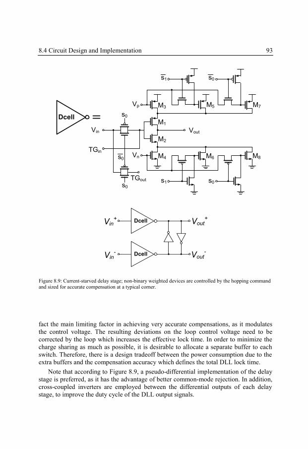
8.4 Circuit Design and Implementation 93
fact the main limiting factor in achieving very accurate compensations, as it modulates
the control voltage. The resulting deviations on the loop control voltage need to be
corrected by the loop which increases the effective lock time. In order to minimize the
charge sharing as much as possible, it is desirable to allocate a separate buffer to each
switch. Therefore, there is a design tradeoff between the power consumption due to the
extra buffers and the compensation accuracy which defines the total DLL lock time.
Note that according to Figure 8.9, a pseudo-differential implementation of the delay
stage is preferred, as it has the advantage of better common-mode rejection. In addition,
cross-coupled inverters are employed between the differential outputs of each delay
stage, to improve the duty cycle of the DLL output signals.
Dcell
Vp
Vin Vout
TGin
TGout
s0
s0
M1
M2
M3
M4Vns0 M6
M5 M7
s0s1
s1 s0
M8
Dcell
Dcell
Vin+
Vin-
Vout+
Vout-
Figure 8.9: Current-starved delay stage; non-binary weighted devices are controlled by the hopping command and sized for accurate compensation at a typical corner.
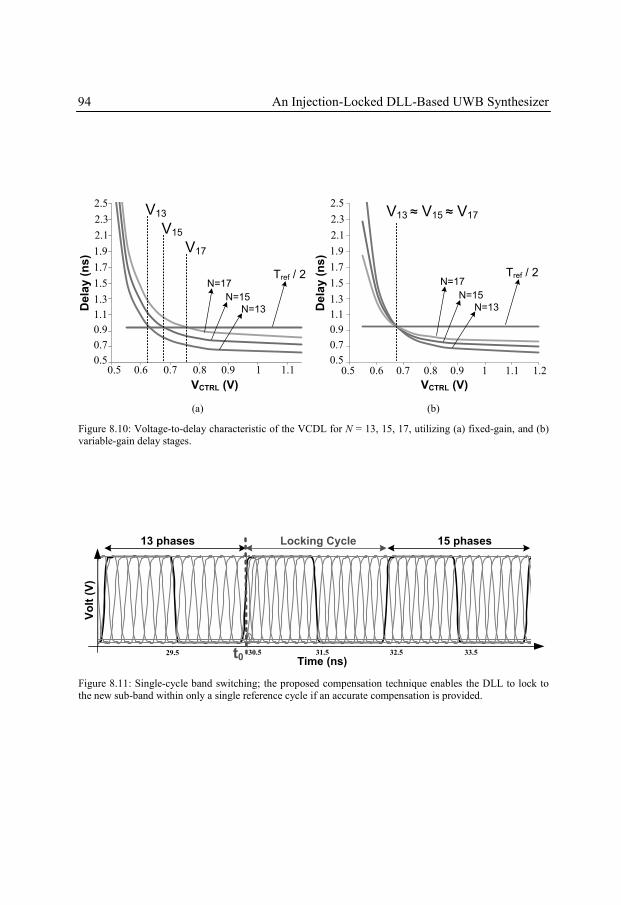
94 An Injection-Locked DLL-Based UWB Synthesizer
500
700
900
1100
1300
1500
1700
1900
2100
2300
2500
500 600 700 800 900 1000 1100 1200
N=13
N=15
N=17
Period/2
500
700
900
1100
1300
1500
1700
1900
2100
2300
2500
550 650 750 850 950 1050 1150
N=13
N=15
N=17
Period/2
VCTRL (V)
0.5 0.6 0.7 0.8 0.9 1 1.1 1.2
VCTRL (V)
0.5
0.7
0.9
1.1
1.3
1.5
1.7
1.9
2.1
2.3
2.5
De
lay
(n
s)
N = 13
N = 15
N = 17
T / 2
N=13
N=15
N=17Tref / 2
V13 ≈ V15 ≈ V17V13
V15
V17
0.5 0.6 0.7 0.8 0.9 1 1.1
De
lay
(n
s)
0.5
0.7
0.9
1.1
1.3
1.5
1.7
1.9
2.1
2.3
2.5
N=13
N=15
N=17Tref / 2
(a) (b)
Figure 8.10: Voltage-to-delay characteristic of the VCDL for N = 13, 15, 17, utilizing (a) fixed-gain, and (b) variable-gain delay stages.
-5.00E-02
1.50E-01
3.50E-01
5.50E-01
7.50E-01
9.50E-01
1.15E+00
2.85E-08 2.95E-08 3.05E-08 3.15E-08 3.25E-08 3.35E-08
13 phases 15 phasesLocking Cycle
t0
Vo
lt (
V)
Time (ns)29.5 30.5 31.5 32.5 33.5
Figure 8.11: Single-cycle band switching; the proposed compensation technique enables the DLL to lock to the new sub-band within only a single reference cycle if an accurate compensation is provided.
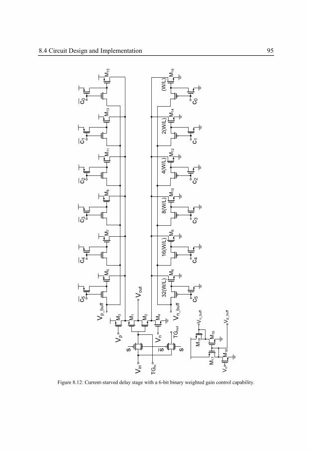
8.4 Circuit Design and Implementation 95
Vn
M19 M
16
M17 M
18
Vn
_b
uff
Vp
_b
uff
Vp
Vin
Vout
TG
in
TG
ou
t
s s sV
n_buff
M1
M2
M3
M4
M5
M6
M7
M8
M9
M11
M10
M12
M13
M15
c0
M14
M16
c1
c2
c3
c4
c5
c0
c1
c2
c3
c4
c5
Vp_buff
Vn
(W/L
)2
(W/L
)4
(W/L
)8
(W/L
)1
6(W
/L)
32
(W/L
)
Figure 8.12: Current-starved delay stage with a 6-bit binary weighted gain control capability.
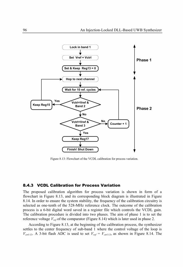
96 An Injection-Locked DLL-Based UWB Synthesizer
8.4.3 VCDL Calibration for Process Variation
The proposed calibration algorithm for process variation is shown in form of a
flowchart in Figure 8.13, and its corresponding block diagram is illustrated in Figure
8.14. In order to ensure the system stability, the frequency of the calibration circuitry is
selected as one-tenth of the 528-MHz reference clock. The outcome of the calibration
process is a 6-bit digital word saved in a register file which controls the VCDL gain.
The calibration procedure is divided into two phases. The aim of phase 1 is to set the
reference voltage Vref of the comparator (Figure 8.14) which is later used in phase 2.
According to Figure 8.13, at the beginning of the calibration process, the synthesizer
settles to the center frequency of sub-band 1 where the control voltage of the loop is
Vctrl-13. A 3-bit flash ADC is used to set Vref = Vctrl-13, as shown in Figure 8.14. The
Lock in band 1
Set Vref = Vctrl
Hop to next channel
No
No
Keep Reg15
Yes
Counter + 1
Finish! Shut Down
Keep Reg17
Vctrl<Vref &
Band 3
Yes
Wait for 10 ref. cycles
Vctrl<Vref &
Band 2
Set & Keep Reg13 = 0
Phase 1
Phase 2
Figure 8.13: Flowchart of the VCDL calibration for process variation.
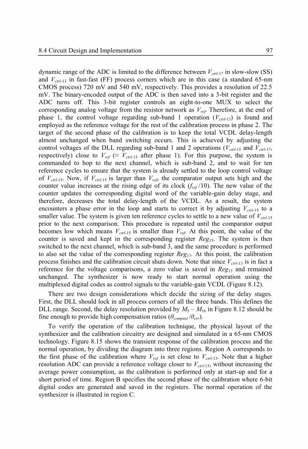
8.4 Circuit Design and Implementation 97
dynamic range of the ADC is limited to the difference between Vctrl-17 in slow-slow (SS)
and Vctrl-13 in fast-fast (FF) process corners which are in this case (a standard 65-nm
CMOS process) 720 mV and 540 mV, respectively. This provides a resolution of 22.5
mV. The binary-encoded output of the ADC is then saved into a 3-bit register and the
ADC turns off. This 3-bit register controls an eight-to-one MUX to select the
corresponding analog voltage from the resistor network as Vref. Therefore, at the end of
phase 1, the control voltage regarding sub-band 1 operation (Vctrl-13) is found and
employed as the reference voltage for the rest of the calibration process in phase 2. The
target of the second phase of the calibration is to keep the total VCDL delay-length
almost unchanged when band switching occurs. This is achieved by adjusting the
control voltages of the DLL regarding sub-band 1 and 2 operations (Vctrl-15 and Vctrl-17,
respectively) close to Vref (≈ Vctrl-13 after phase 1). For this purpose, the system is
commanded to hop to the next channel, which is sub-band 2, and to wait for ten
reference cycles to ensure that the system is already settled to the loop control voltage
of Vctrl-15. Now, if Vctrl-15 is larger than Vref, the comparator output sets high and the
counter value increases at the rising edge of its clock (fref /10). The new value of the
counter updates the corresponding digital word of the variable-gain delay stage, and
therefore, decreases the total delay-length of the VCDL. As a result, the system
encounters a phase error in the loop and starts to correct it by adjusting Vctrl-15 to a
smaller value. The system is given ten reference cycles to settle to a new value of Vctrl-15
prior to the next comparison. This procedure is repeated until the comparator output
becomes low which means Vctrl-15 is smaller than Vref. At this point, the value of the
counter is saved and kept in the corresponding register Reg15. The system is then
switched to the next channel, which is sub-band 3, and the same procedure is performed
to also set the value of the corresponding register Reg17. At this point, the calibration
process finishes and the calibration circuit shuts down. Note that since Vctrl-13 is in fact a
reference for the voltage comparisons, a zero value is saved in Reg13 and remained
unchanged. The synthesizer is now ready to start normal operation using the
multiplexed digital codes as control signals to the variable-gain VCDL (Figure 8.12).
There are two design considerations which decide the sizing of the delay stages.
First, the DLL should lock in all process corners of all the three bands. This defines the
DLL range. Second, the delay resolution provided by M5 ‒ M16 in Figure 8.12 should be
fine enough to provide high compensation ratios (θcompnst /θerr).
To verify the operation of the calibration technique, the physical layout of the
synthesizer and the calibration circuitry are designed and simulated in a 65-nm CMOS
technology. Figure 8.15 shows the transient response of the calibration process and the
normal operation, by dividing the diagram into three regions. Region A corresponds to
the first phase of the calibration where Vref is set close to Vctrl-13. Note that a higher
resolution ADC can provide a reference voltage closer to Vctrl-13, without increasing the
average power consumption, as the calibration is performed only at start-up and for a
short period of time. Region B specifies the second phase of the calibration where 6-bit
digital codes are generated and saved in the registers. The normal operation of the
synthesizer is illustrated in region C.
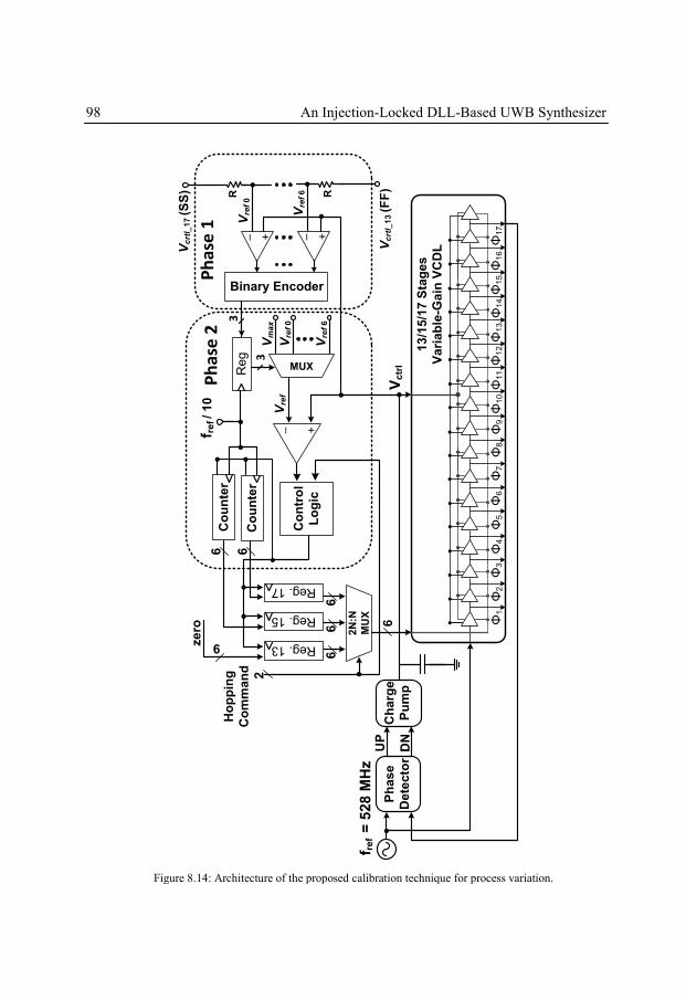
98 An Injection-Locked DLL-Based UWB Synthesizer
6
2N
:N
MU
X
66
6
Vctr
l
_ +
Vre
f
Reg. 13
Reg. 15
Reg. 17
6C
ou
nte
r
f ref / 10
Co
ntr
ol
Lo
gic
_ + _ +
R R
Vc
rtl_
13
(F
F)
Vre
f 0
Vre
f 6
Binary EncoderV
ref
0
Vre
f 6
Vm
ax
Reg
3
3
Ph
ase
1P
has
e 2
Vc
rtl_
17
(S
S)
Co
un
ter
6
6
2
Ho
pp
ing
Co
mm
an
d
13
/15/1
7 S
tag
es
Vari
ab
le-G
ain
VC
DL
Φ1
Φ2
Φ1
7Φ
5Φ
7Φ
3Φ
4Φ
6Φ
8Φ
9Φ
12
Φ1
4Φ
10
Φ1
1Φ
13
Φ1
5Φ
16
Ph
ase
Dete
cto
r
f ref
= 5
28
MH
zU
P
DN
MUX
Ch
arg
e
Pu
mp
zero
Figure 8.14: Architecture of the proposed calibration technique for process variation.
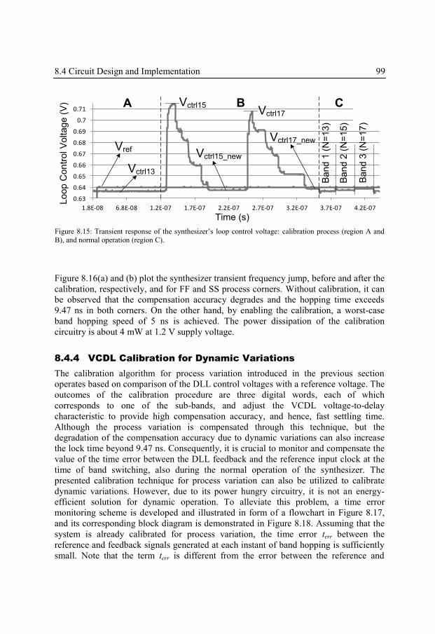
8.4 Circuit Design and Implementation 99
Figure 8.16(a) and (b) plot the synthesizer transient frequency jump, before and after the
calibration, respectively, and for FF and SS process corners. Without calibration, it can
be observed that the compensation accuracy degrades and the hopping time exceeds
9.47 ns in both corners. On the other hand, by enabling the calibration, a worst-case
band hopping speed of 5 ns is achieved. The power dissipation of the calibration
circuitry is about 4 mW at 1.2 V supply voltage.
8.4.4 VCDL Calibration for Dynamic Variations
The calibration algorithm for process variation introduced in the previous section
operates based on comparison of the DLL control voltages with a reference voltage. The
outcomes of the calibration procedure are three digital words, each of which
corresponds to one of the sub-bands, and adjust the VCDL voltage-to-delay
characteristic to provide high compensation accuracy, and hence, fast settling time.
Although the process variation is compensated through this technique, but the
degradation of the compensation accuracy due to dynamic variations can also increase
the lock time beyond 9.47 ns. Consequently, it is crucial to monitor and compensate the
value of the time error between the DLL feedback and the reference input clock at the
time of band switching, also during the normal operation of the synthesizer. The
presented calibration technique for process variation can also be utilized to calibrate
dynamic variations. However, due to its power hungry circuitry, it is not an energy-
efficient solution for dynamic operation. To alleviate this problem, a time error
monitoring scheme is developed and illustrated in form of a flowchart in Figure 8.17,
and its corresponding block diagram is demonstrated in Figure 8.18. Assuming that the
system is already calibrated for process variation, the time error terr between the
reference and feedback signals generated at each instant of band hopping is sufficiently
small. Note that the term terr is different from the error between the reference and
0.63
0.64
0.65
0.66
0.67
0.68
0.69
0.7
0.71
1.8E-08 6.8E-08 1.2E-07 1.7E-07 2.2E-07 2.7E-07 3.2E-07 3.7E-07 4.2E-07
Vctrl (V)
Vref (V)
Time (s)
A B CVctrl15
Vctrl15_new
Vctrl13
Vctrl17
Vctrl17_new
Ba
nd
1 (
N=
13
)
Ba
nd
2 (
N=
15
)
Ba
nd
3 (
N=
17
)
Lo
op
Co
ntr
ol V
olta
ge
(V
)
Vref
Figure 8.15: Transient response of the synthesizer’s loop control voltage: calibration process (region A and
B), and normal operation (region C).
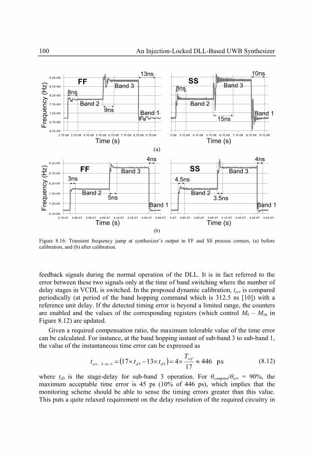
100 An Injection-Locked DLL-Based UWB Synthesizer
feedback signals during the normal operation of the DLL. It is in fact referred to the
error between these two signals only at the time of band switching where the number of
delay stages in VCDL is switched. In the proposed dynamic calibration, terr is compared
periodically (at period of the band hopping command which is 312.5 ns [10]) with a
reference unit delay. If the detected timing error is beyond a limited range, the counters
are enabled and the values of the corresponding registers (which control M5 ‒ M16 in
Figure 8.12) are updated.
Given a required compensation ratio, the maximum tolerable value of the time error
can be calculated. For instance, at the band hopping instant of sub-band 3 to sub-band 1,
the value of the instantaneous time error can be expressed as
ps44617
41317 3313,
ref
ddtoerr
Tttt (8.12)
where td3 is the stage-delay for sub-band 3 operation. For θcompnst/θerr = 90%, the
maximum acceptable time error is 45 ps (10% of 446 ps), which implies that the
monitoring scheme should be able to sense the timing errors greater than this value.
This puts a quite relaxed requirement on the delay resolution of the required circuitry in
6.2E+09
6.7E+09
7.2E+09
7.7E+09
8.2E+09
8.7E+09
9.2E+09
2.7E-08 3.7E-08 4.7E-08 5.7E-08 6.7E-08 7.7E-08 8.7E-08 9.7E-08
6.2E+09
6.7E+09
7.2E+09
7.7E+09
8.2E+09
8.7E+09
9.2E+09
2.7E-08 3.7E-08 4.7E-08 5.7E-08 6.7E-08 7.7E-08 8.7E-08 9.7E-08
FF SS
Fre
qu
en
cy (
Hz)
Time (s)
10ns13ns
9ns
8ns8ns
15ns
Band 2
Band 3
Band 1
Band 2
Band 3
Band 1
Time (s) (a)
6.7E+09
7.2E+09
7.7E+09
8.2E+09
8.7E+09
9.2E+09
3.7E-07 3.8E-07 3.9E-07 4.0E-07 4.1E-07 4.2E-07 4.3E-07 4.4E-07
6.7E+09
7.2E+09
7.7E+09
8.2E+09
8.7E+09
9.2E+09
3.7E-07 3.8E-07 3.9E-07 4.0E-07 4.1E-07 4.2E-07 4.3E-07 4.4E-07
FF SS
3ns
5ns
4ns
4.5ns
3.5ns
4ns
Band 2
Band 3
Band 1
Band 2
Band 3
Band 1
Fre
quency (
Hz)
Time (s) Time (s) (b)
Figure 8.16: Transient frequency jump at synthesizer’s output in FF and SS process corners, (a) before
calibration, and (b) after calibration.
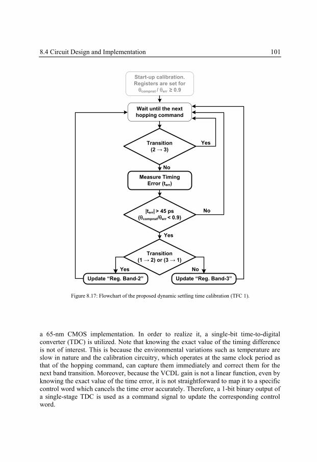
8.4 Circuit Design and Implementation 101
a 65-nm CMOS implementation. In order to realize it, a single-bit time-to-digital
converter (TDC) is utilized. Note that knowing the exact value of the timing difference
is not of interest. This is because the environmental variations such as temperature are
slow in nature and the calibration circuitry, which operates at the same clock period as
that of the hopping command, can capture them immediately and correct them for the
next band transition. Moreover, because the VCDL gain is not a linear function, even by
knowing the exact value of the time error, it is not straightforward to map it to a specific
control word which cancels the time error accurately. Therefore, a 1-bit binary output of
a single-stage TDC is used as a command signal to update the corresponding control
word.
Start-up calibration.
Registers are set for
θcompnst / θerr ≥ 0.9
Wait until the next
hopping command
No
No
Yes
Update “Reg. Band-2”
Transition
(2 → 3)
Measure Timing
Error (terr)
|terr| > 45 ps
(θcompnst/θerr < 0.9)
Transition
(1 → 2) or (3 → 1)
Update “Reg. Band-3”
Yes
NoYes
Figure 8.17: Flowchart of the proposed dynamic settling time calibration (TFC 1).
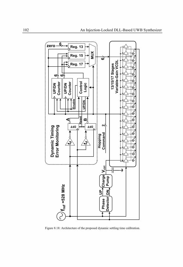
102 An Injection-Locked DLL-Based UWB Synthesizer
Reg. 15
Reg. 176
UP
/DN
Co
un
ter
Co
ntr
ol
Lo
gic
t d
Dy
na
mic
Tim
ing
Err
or
Mo
nit
ori
ng
A B
DFF DFF
MU
X
t d
Res
et
UP
/DN
Co
un
ter
6
En
ab
le
UP
/DN
13
/15
/17
Sta
ge
s
Va
ria
ble
-Ga
in V
CD
L
Φ1
Φ2
Φ1
7Φ
5Φ
7Φ
3Φ
4Φ
6Φ
8Φ
9Φ
12
Φ1
4Φ
10
Φ1
1Φ
13
Φ1
5Φ
16
Ph
as
e
De
tec
tor
f re
f =
528
MH
z
UP
DN
Ch
arg
e
Pu
mp
2H
op
pin
g
Co
mm
an
d
6
Reg. 136zero
Vc
trl
Figure 8.18: Architecture of the proposed dynamic settling time calibration.
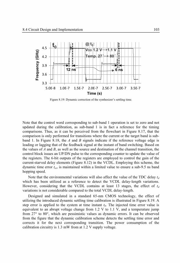
8.4 Circuit Design and Implementation 103
Note that the control word corresponding to sub-band 1 operation is set to zero and not
updated during the calibration, as sub-band 1 is in fact a reference for the timing
comparisons. Thus, as it can be perceived from the flowchart in Figure 8.17, that the
comparison is only performed for transitions where the current or the target band is sub-
band 1. In Figure 8.18, the A and B signals indicate if the reference voltage edge is
leading or lagging that of the feedback signal at the instant of band switching. Based on
the values of A and B, as well as the source and destination of the channel transition, the
control block issues an UP/DN pulse to the corresponding counter to update the value of
the registers. The 6-bit outputs of the registers are employed to control the gain of the
current-starved delay elements (Figure 8.12) in the VCDL. Employing this scheme, the
dynamic time error terr is maintained within a limited value to ensure a sub-9.5 ns band
hopping speed.
Note that the environmental variations will also affect the value of the TDC delay td
which has been utilized as a reference to detect the VCDL delay-length variations.
However, considering that the VCDL contains at least 13 stages, the effect of td
variations is not considerable compared to the total VCDL delay-length.
Designed and simulated in a standard 65-nm CMOS technology, the effect of
utilizing the introduced dynamic settling time calibration is illustrated in Figure 8.19. A
step error is applied to the system at time instant t0. The injected time error value is
equivalent to an abrupt voltage change from 1.2 V to 1.1 V, and a temperature jump
from 27° to 80°, which are pessimistic values as dynamic errors. It can be observed
from the figure that the dynamic calibration scheme detects the settling time error and
corrects it for the next corresponding transition. The power consumption of the
calibration circuitry is 1.3 mW from at 1.2 V supply voltage.
3.3
3.6
3.9
4.2
4.5
5.0E-8 1.0E-7 1.5E-7 2.0E-7 2.5E-7 3.0E-7 3.5E-7
t0
12 ns 6 ns
@ t0:
VDD 1.2 V→1.1 V
Temp. 27 ̊→ 80 ̊
Time (s)
Fre
qu
en
cy (
GH
z)
Figure 8.19: Dynamic correction of the synthesizer’s settling time.
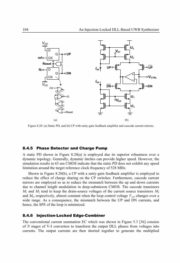
104 An Injection-Locked DLL-Based UWB Synthesizer
8.4.5 Phase Detector and Charge Pump
A static PD shown in Figure 8.20(a) is employed due its superior robustness over a
dynamic topology. Generally, dynamic latches can provide higher speed. However, the
simulation results in 65 nm CMOS indicate that the static PD does not exhibit any speed
limitation around the target reference clock frequency of 528 MHz.
Shown in Figure 8.20(b), a CP with a unity-gain feedback amplifier is employed to
reduce the effect of charge sharing on the CP switches. Furthermore, cascode current
mirrors are employed so as to reduce the mismatch between the up and down currents
due to channel length modulation in deep-submicron CMOS. The cascode transistors
M1 and M2 tend to keep the drain-source voltages of the current source transistors M3
and M4, respectively, almost constant when the loop control voltage Vctrl changes over a
wide range. As a consequence, the mismatch between the UP and DN currents, and
hence, the SPE of the loop is minimized.
8.4.6 Injection-Locked Edge-Combiner
The conventional current summation EC which was shown in Figure 5.3 [36] consists
of N stages of V-I converters to transform the output DLL phases from voltages into
currents. The output currents are then shorted together to generate the multiplied
Reset
CK
Q
D
Q
CK
VDD
Reset
ref
D
Q
CK
VDD
fb
UP
DN
+
-
UP UP
DNDN
Icp
Vb1
Vb2
VCTRL
Icp
M1
M2
M3
M4
(a) (b)
Figure 8.20: (a) Static PD, and (b) CP with unity-gain feedback amplifier and cascode current mirrors.
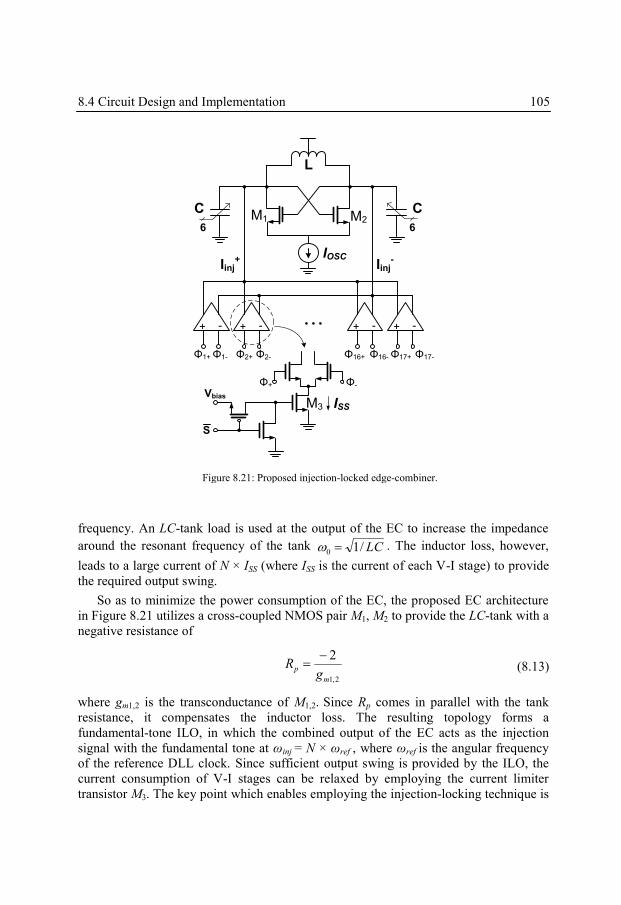
8.4 Circuit Design and Implementation 105
frequency. An LC-tank load is used at the output of the EC to increase the impedance
around the resonant frequency of the tank LC/10 . The inductor loss, however,
leads to a large current of N × ISS (where ISS is the current of each V-I stage) to provide
the required output swing.
So as to minimize the power consumption of the EC, the proposed EC architecture
in Figure 8.21 utilizes a cross-coupled NMOS pair M1, M2 to provide the LC-tank with a
negative resistance of
2,1
2
m
pg
R
(8.13)
where gm1,2 is the transconductance of M1,2. Since Rp comes in parallel with the tank
resistance, it compensates the inductor loss. The resulting topology forms a
fundamental-tone ILO, in which the combined output of the EC acts as the injection
signal with the fundamental tone at ωinj = N × ωref , where ωref is the angular frequency
of the reference DLL clock. Since sufficient output swing is provided by the ILO, the
current consumption of V-I stages can be relaxed by employing the current limiter
transistor M3. The key point which enables employing the injection-locking technique is
+ -
Φ1+
+ -+ - + -
M2M1
L
C C
ISS
IOSC
Φ1- Φ2+ Φ2- Φ16+ Φ16- Φ17+ Φ17-
Φ+ Φ-
S
Vbias
Iinj+
Iinj-
6 6
M3
Figure 8.21: Proposed injection-locked edge-combiner.
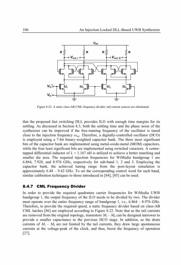
106 An Injection-Locked DLL-Based UWB Synthesizer
that the proposed fast switching DLL provides ILO with enough time margins for its
settling. As discussed in Section 8.3, both the settling time and the phase noise of the
synthesizer can be improved if the free-running frequency of the oscillator is tuned
close to the injection frequency ωinj. Therefore, a digitally-controlled oscillator (DCO)
is employed using a 7-bit binary-weighted capacitor bank. The three most significant
bits of the capacitor bank are implemented using metal-oxide-metal (MOM) capacitors,
while the four least significant bits are implemented using switched varactors. A center-
tapped differential inductor of L = 1.167 nH is utilized to achieve a better matching and
smaller die area. The required injection frequencies for WiMedia bandgroup 1 are
6.864, 7.920, and 8.976 GHz, respectively for sub-band 1, 2 and 3. Employing the
capacitor bank, the achieved tuning range from the post-layout simulation is
approximately 6.48 ‒ 9.42 GHz. To set the corresponding control word for each band,
similar calibration techniques to those introduced in [84], [85] can be used.
8.4.7 CML Frequency Divider
In order to provide the required quadrature carrier frequencies for WiMedia UWB
bandgroup 1, the output frequency of the ILO needs to be divided by two. The divider
must operate over the entire frequency range of bandgroup 1, i.e., 6.864 ‒ 8.976 GHz.
Therefore, to provide the required speed, a static frequency divider based on class-AB
CML latches [86] are employed according to Figure 8.22. Note that as the tail currents
are removed from the original topology, transistors M1 ‒ M4 can be designed narrower to
provide a smaller capacitance to the previous DCO stage. In addition, as the drain
currents of M1 ‒ M4 are not limited by the tail currents, they draw large spontaneous
currents at the voltage-peak of the clock, and thus, boost the frequency of operation
[27].
Vin+
Vin-
RR RR
VDD
Vout, I Vout, Q
M1 M2 M3 M4
Figure 8.22: A static class-AB CML frequency divider; tail current sources are eliminated.

8.5 Experimental Results 107
8.5 Experimental Results
The introduced DLL-based injection-locked UWB synthesizer is designed and
implemented in a 65-nm CMOS process. The calibration is done offline and the digital
codes are written through an on-chip serial input pin into a shift register which is shown
in Figure 8.23. The digital control bits are divided into two groups, each of which
correspond to one of the sub-bands and selected through a MUX which is controlled by
the hopping command. As the hopping time is critical, the select signal of the MUX is
excessively buffered to provide sharp edges.
The post-layout simulation of the synthesizer’s phase noise in sub-band 3 of
WiMedia bandgroup 1 is shown in Figure 8.24 for the free-running oscillator at 4471
MHz, injection-locked oscillator at 4488 MHz and the reference clock at 528 MHz.
Under injection locking, the simulated phase noise is ‒112.1 and ‒121.6 dBc/Hz,
respectively at 100 kHz and 1 MHz offset from the carrier frequency of 4488 MHz. In
free running and for the same offset frequencies, the phase noise is ‒72.9 and ‒99.8
dBc/Hz, respectively. Figure 8.25 demonstrates the synthesizer’s transient frequency
jump for all six possible band transitions in WiMedia UWB (Table 2-1), representing a
worst-case hopping speed of 5.49 ns.
The chip micrograph of the UWB synthesizer and the designed printed circuit board
(PCB) are shown in Figure 8.26 and Figure 8.27, respectively. The chip includes the
DLL, EC, ILO, CML divider and open-drain output stages. In order to reduce the effect
of supply noise generated by the switching activities of the digital circuitries such as
input and output buffers, separate on-chip and on-board supply rails are dedicated to
sensitive radio frequency (RF) circuitries such as ILO and CML divider. In addition, to
further reduce the noise-coupling through the substrate, two separate rails are employed
for the substrate and ground of noisy digital circuits on the chip. Due to the high
Shift
Register
Serial In
Serial Out
2N:N
MUX
N
N
N
CLKHopping
Command
To
DCO / VCDL
Figure 8.23: On-chip circuitry for band hopping test.
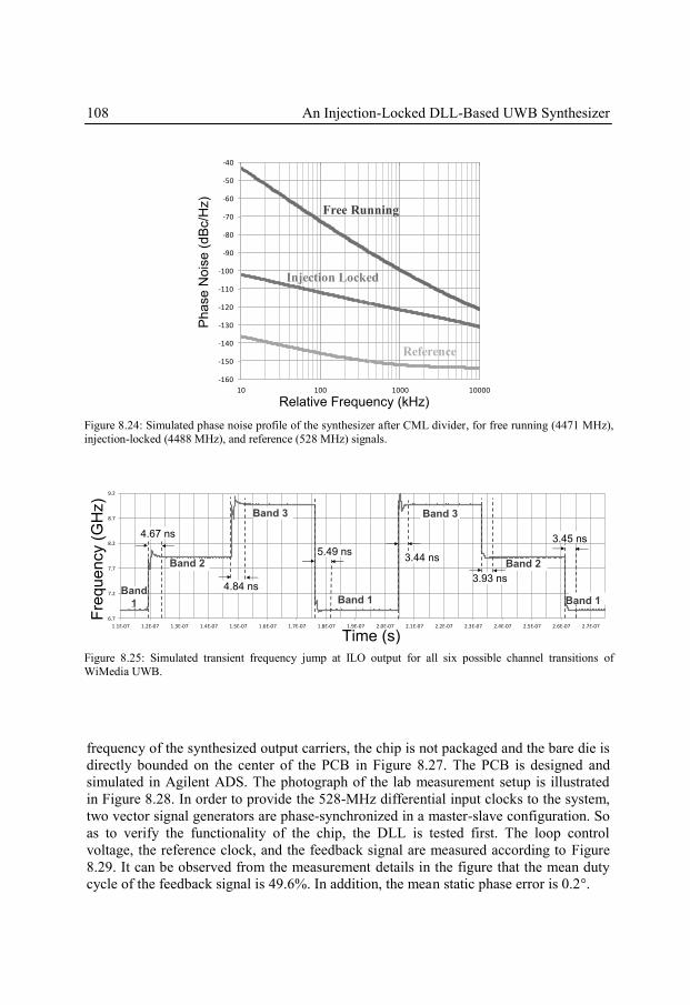
108 An Injection-Locked DLL-Based UWB Synthesizer
frequency of the synthesized output carriers, the chip is not packaged and the bare die is
directly bounded on the center of the PCB in Figure 8.27. The PCB is designed and
simulated in Agilent ADS. The photograph of the lab measurement setup is illustrated
in Figure 8.28. In order to provide the 528-MHz differential input clocks to the system,
two vector signal generators are phase-synchronized in a master-slave configuration. So
as to verify the functionality of the chip, the DLL is tested first. The loop control
voltage, the reference clock, and the feedback signal are measured according to Figure
8.29. It can be observed from the measurement details in the figure that the mean duty
cycle of the feedback signal is 49.6%. In addition, the mean static phase error is 0.2°.
-160
-150
-140
-130
-120
-110
-100
-90
-80
-70
-60
-50
-40
10 100 1000 10000
Reference
Free Running
Injection Locked
Relative Frequency (kHz)
Ph
ase
No
ise
(dB
c/H
z)P
ha
se
No
ise
(d
Bc/H
z)
Relative Frequency (kHz)
Figure 8.24: Simulated phase noise profile of the synthesizer after CML divider, for free running (4471 MHz),
injection-locked (4488 MHz), and reference (528 MHz) signals.
6.7
7.2
7.7
8.2
8.7
9.2
1.1E-07 1.2E-07 1.3E-07 1.4E-07 1.5E-07 1.6E-07 1.7E-07 1.8E-07 1.9E-07 2.0E-07 2.1E-07 2.2E-07 2.3E-07 2.4E-07 2.5E-07 2.6E-07 2.7E-07
4.67 ns
4.84 ns
5.49 ns3.44 ns
3.93 ns
3.45 ns
Band 2
Band 3
Band 1
Band 3
Band 2
Band 1Band
1Fre
qu
ency
(G
Hz)
Time (s)
3.93 ns
4.67 ns
4.84 ns
5.49 ns3.44 ns
3.45 ns
Time (s)
Fre
qu
en
cy (
GH
z)
Band 2
Band 3
Band 1
Band 3
Band 2
Band 1Band
1
Figure 8.25: Simulated transient frequency jump at ILO output for all six possible channel transitions of
WiMedia UWB.
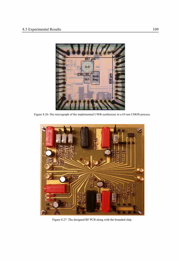
8.5 Experimental Results 109
907 μm
83
0 μ
m
DLLShift
Reg.
EC
ILO
CML
Figure 8.26: Die micrograph of the implemented UWB synthesizer in a 65-nm CMOS process.
Figure 8.27: The designed RF PCB along with the bounded chip.
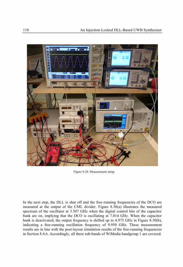
110 An Injection-Locked DLL-Based UWB Synthesizer
In the next step, the DLL is shut off and the free-running frequencies of the DCO are
measured at the output of the CML divider. Figure 8.30(a) illustrates the measured
spectrum of the oscillator at 3.507 GHz when the digital control bits of the capacitor
bank are on, implying that the DCO is oscillating at 7.014 GHz. When the capacitor
bank is deactivated, the output frequency is shifted up to 4.975 GHz in Figure 8.30(b),
indicating a free-running oscillation frequency of 9.950 GHz. These measurement
results are in line with the post-layout simulation results of the free-running frequencies
in Section 8.4.6. Accordingly, all three sub-bands of WiMedia bandgroup 1 are covered.
Figure 8.28: Measurement setup.
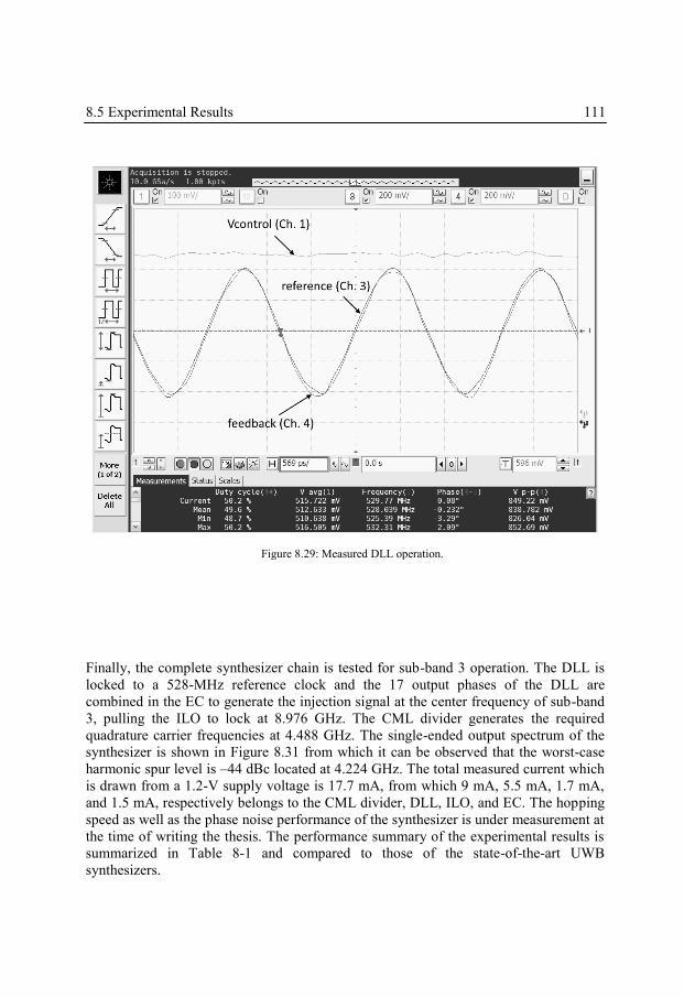
8.5 Experimental Results 111
Finally, the complete synthesizer chain is tested for sub-band 3 operation. The DLL is
locked to a 528-MHz reference clock and the 17 output phases of the DLL are
combined in the EC to generate the injection signal at the center frequency of sub-band
3, pulling the ILO to lock at 8.976 GHz. The CML divider generates the required
quadrature carrier frequencies at 4.488 GHz. The single-ended output spectrum of the
synthesizer is shown in Figure 8.31 from which it can be observed that the worst-case
harmonic spur level is ‒44 dBc located at 4.224 GHz. The total measured current which
is drawn from a 1.2-V supply voltage is 17.7 mA, from which 9 mA, 5.5 mA, 1.7 mA,
and 1.5 mA, respectively belongs to the CML divider, DLL, ILO, and EC. The hopping
speed as well as the phase noise performance of the synthesizer is under measurement at
the time of writing the thesis. The performance summary of the experimental results is
summarized in Table 8-1 and compared to those of the state-of-the-art UWB
synthesizers.
Figure 8.29: Measured DLL operation.
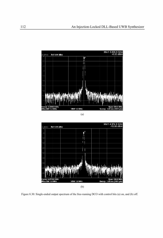
112 An Injection-Locked DLL-Based UWB Synthesizer
(a)
(b)
Figure 8.30: Single-ended output spectrum of the free-running DCO with control bits (a) on, and (b) off.
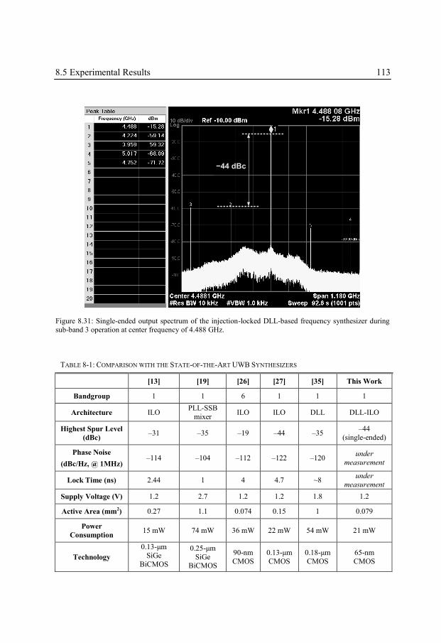
8.5 Experimental Results 113
−44 dBc
Figure 8.31: Single-ended output spectrum of the injection-locked DLL-based frequency synthesizer during
sub-band 3 operation at center frequency of 4.488 GHz.
TABLE 8-1: COMPARISON WITH THE STATE-OF-THE-ART UWB SYNTHESIZERS
[13] [19] [26] [27] [35] This Work
Bandgroup 1 1 6 1 1 1
Architecture ILO PLL-SSB
mixer ILO ILO DLL DLL-ILO
Highest Spur Level
(dBc) ‒31 ‒35 ‒19 ‒44 ‒35
‒44
(single-ended)
Phase Noise
(dBc/Hz, @ 1MHz) ‒114 ‒104 ‒112 ‒122 ‒120
under
measurement
Lock Time (ns) 2.44 1 4 4.7 ~8 under
measurement
Supply Voltage (V) 1.2 2.7 1.2 1.2 1.8 1.2
Active Area (mm2) 0.27 1.1 0.074 0.15 1 0.079
Power
Consumption 15 mW 74 mW 36 mW 22 mW 54 mW 21 mW
Technology
0.13-μm
SiGe
BiCMOS
0.25-μm
SiGe BiCMOS
90-nm
CMOS
0.13-μm
CMOS
0.18-μm
CMOS
65-nm
CMOS
114 An Injection-Locked DLL-Based UWB Synthesizer
8.6 Summary
A new architecture for fast hopping frequency synthesis based on edge-combing DLL
and injection-locking approach is introduced. A variable-stage VCDL with a symmetric
bypass mechanism is presented which utilizes programmable-gain current-starved delay
stages to provide open-loop phase compensations at the time of band hopping, to keep
the total VCDL delay-length constant. As a result, a small hopping time is achieved.
Two calibration algorithms are developed to guarantee the robustness of the scheme in
presence of PVT variations. Moreover, an ILO is utilized at the output of the EC to
reduce the power consumption of the multistage V-I converter. The synthesizer is
designed and implemented in a 65-nm CMOS technology, and the preliminary
measurement results verify the functionality of the synthesizer and indicate that the
spurious performance, the power consumption, and the active silicon area of the
synthesizer is competitive to those of the state-of-the-art implementations. The band
hopping speed and phase noise of the synthesizer are under the measurement at the time
of writing the thesis.
115
Chapter 9
Fast Hopping DLL-Based
Frequency Synthesis using T/H
9.1 Introduction
Conventional DLL-based frequency synthesizers achieve fast channel switching by
taking advantage of the first-order stability of the DLL and utilizing a relatively wide
loop bandwidth. A large loop-gain can be provided through biasing the VCDL in high-
gain regions of its transfer function. This leads to higher noise amplification by the
VCDL which deteriorates the spectral purity of the synthesizer. Furthermore, there is a
tradeoff between the loop bandwidth and the level of ripples on the loop control voltage.
This implies that a wide loop bandwidth also gives rise to the level of sideband spurs.
This chapter covers [7] to present a fast switching DLL-based technique for
frequency synthesis in bandgroup 1 of WiMedia UWB communication. The proposed
architecture employs the concept of T/H to sample the lock control voltages of the three
sub-bands and store them across three capacitors during a start-up phase. In normal
operation when the hopping command arrives, the corresponding stored voltage is
applied to the loop in an open-loop regime to achieve a band hopping speed of less than
9.5 ns. Certain architectural and circuit techniques are utilized in order to minimize the
error in the sampled voltages caused by channel charge injection and clock feedthrough
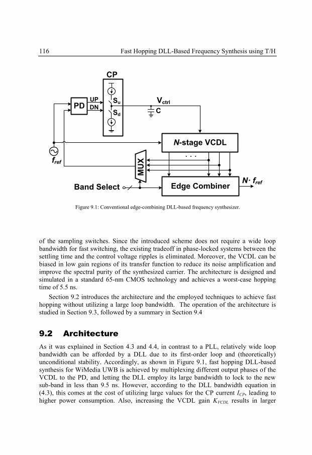
116 Fast Hopping DLL-Based Frequency Synthesis using T/H
of the sampling switches. Since the introduced scheme does not require a wide loop
bandwidth for fast switching, the existing tradeoff in phase-locked systems between the
settling time and the control voltage ripples is eliminated. Moreover, the VCDL can be
biased in low gain regions of its transfer function to reduce its noise amplification and
improve the spectral purity of the synthesized carrier. The architecture is designed and
simulated in a standard 65-nm CMOS technology and achieves a worst-case hopping
time of 5.5 ns.
Section 9.2 introduces the architecture and the employed techniques to achieve fast
hopping without utilizing a large loop bandwidth. The operation of the architecture is
studied in Section 9.3, followed by a summary in Section 9.4
9.2 Architecture
As it was explained in Section 4.3 and 4.4, in contrast to a PLL, relatively wide loop
bandwidth can be afforded by a DLL due to its first-order loop and (theoretically)
unconditional stability. Accordingly, as shown in Figure 9.1, fast hopping DLL-based
synthesis for WiMedia UWB is achieved by multiplexing different output phases of the
VCDL to the PD, and letting the DLL employ its large bandwidth to lock to the new
sub-band in less than 9.5 ns. However, according to the DLL bandwidth equation in
(4.3), this comes at the cost of utilizing large values for the CP current ICP, leading to
higher power consumption. Also, increasing the VCDL gain KVCDL results in larger
PD
Edge Combiner
UP
DN
N· fref
N-stage VCDL
· · ·
Vctrl
fref
MU
X
C
CP
Su
Sd
Band Select
Figure 9.1: Conventional edge-combining DLL-based frequency synthesizer.
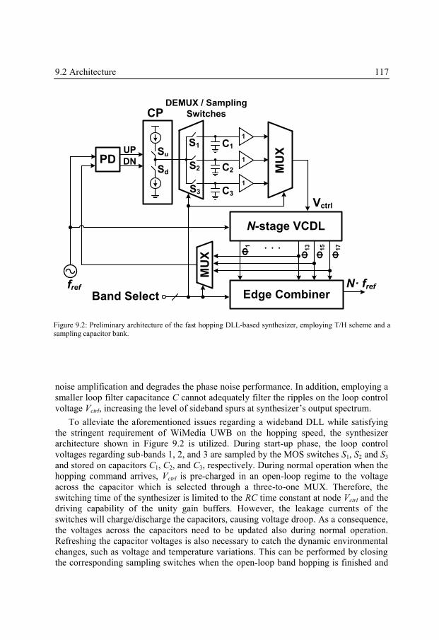
9.2 Architecture 117
noise amplification and degrades the phase noise performance. In addition, employing a
smaller loop filter capacitance C cannot adequately filter the ripples on the loop control
voltage Vctrl, increasing the level of sideband spurs at synthesizer’s output spectrum.
To alleviate the aforementioned issues regarding a wideband DLL while satisfying
the stringent requirement of WiMedia UWB on the hopping speed, the synthesizer
architecture shown in Figure 9.2 is utilized. During start-up phase, the loop control
voltages regarding sub-bands 1, 2, and 3 are sampled by the MOS switches S1, S2 and S3
and stored on capacitors C1, C2, and C3, respectively. During normal operation when the
hopping command arrives, Vctrl is pre-charged in an open-loop regime to the voltage
across the capacitor which is selected through a three-to-one MUX. Therefore, the
switching time of the synthesizer is limited to the RC time constant at node Vctrl and the
driving capability of the unity gain buffers. However, the leakage currents of the
switches will charge/discharge the capacitors, causing voltage droop. As a consequence,
the voltages across the capacitors need to be updated also during normal operation.
Refreshing the capacitor voltages is also necessary to catch the dynamic environmental
changes, such as voltage and temperature variations. This can be performed by closing
the corresponding sampling switches when the open-loop band hopping is finished and
PD
Edge Combiner
UP
DN
N· fref
N-stage VCDL
· · ·
Vctrl
Ф1
Ф1
7
Ф1
5
Ф1
3
MU
X
DEMUX / Sampling
Switches
1
1
1
C1
C2
C3
MU
X
CP
Su
Sd
S1
S2
S3
Band Selectfref
Figure 9.2: Preliminary architecture of the fast hopping DLL-based synthesizer, employing T/H scheme and a sampling capacitor bank.
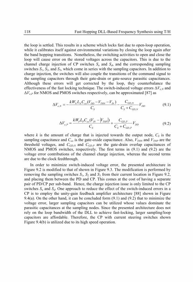
118 Fast Hopping DLL-Based Frequency Synthesis using T/H
the loop is settled. This results in a scheme which locks fast due to open-loop operation,
while it calibrates itself against environmental variations by closing the loop again after
the band hopping transitions. Nonetheless, the switching activities to open and close the
loop will cause error on the stored voltages across the capacitors. This is due to the
channel charge injection of CP switches Su and Sd, and the corresponding sampling
switches S1, S2, and S3, which come in series with the sampling capacitors. In addition to
charge injection, the switches will also couple the transitions of the command signal to
the sampling capacitors through their gate-drain or gate-source parasitic capacitances.
Although these errors will get corrected by the loop, they counterbalance the
effectiveness of the fast locking technique. The switch-induced voltage errors ΔVe,N and
ΔVe,P for NMOS and PMOS switches respectively, can be approximated [87] as
DD
NGDS
NGD
S
INTHNDDoxNNNe V
CC
C
C
VVVCLkWV
,
,
,
)(
(9.1)
DD
PGDS
PGD
S
THPINoxPP
Pe VCC
C
C
VVCLkWV
,
,
,
)(
(9.2)
where k is the amount of charge that is injected towards the output node, CS is the
sampling capacitance and Cox is the gate-oxide capacitance. Also, VTHN and VTHP are the
threshold voltages, and CGD,N and CGD,P are the gate-drain overlap capacitances of
NMOS and PMOS switches, respectively. The first terms in (9.1) and (9.2) are the
voltage error contributions of the channel charge injection, whereas the second terms
are due to the clock feedthrough.
In order to minimize switch-induced voltage error, the presented architecture in
Figure 9.2 is modified to that of shown in Figure 9.3. The modification is performed by
removing the sampling switches S1, S2 and S3 from their current location in Figure 9.2,
and placing them between the PD and CP. This comes at the cost of having a separate
pair of PD/CP per sub-band. Hence, the charge injection issue is only limited to the CP
switches Su and Sd. One approach to reduce the effect of the switch-induced errors in a
CP is to employ the unity-gain feedback amplifier architecture [88] shown in Figure
9.4(a). On the other hand, it can be concluded form (9.1) and (9.2) that to minimize the
voltage error, larger sampling capacitors can be utilized whose values dominate the
parasitic capacitances at the sampling nodes. Since the presented architecture does not
rely on the loop bandwidth of the DLL to achieve fast-locking, larger sampling/loop
capacitors are affordable. Therefore, the CP with current steering switches shown
Figure 9.4(b) is utilized due to its high speed operation.
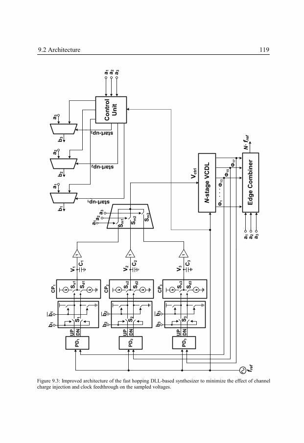
9.2 Architecture 119
Ed
ge C
om
bin
er
N· f r
ef
N-s
tag
e V
CD
L
· ·
·
Vc
trl
Ф1
Ф17
Ф15
Ф13
1 1 1
C1
C2
C3
PD
1
UP
DN
CP
1 Su
1
Sd
1
UP
DN
CP
2 Su
2
Sd
2
UP
DN
CP
3 Su
3
Sd
3
f re
f
b1
b1
b2
b2
b3
b3
a1 a
2a
3
PD
2
PD
3
a1
a2
a3
Co
ntr
ol
Un
it
b1
b2
b3
a1
a2
a3
start-up1
a1
a2
a3
start-up3
start-up2
S1
S2
S3
Sm
1
Sm
2
Sm
3
V1
V2
V3
Figure 9.3: Improved architecture of the fast hopping DLL-based synthesizer to minimize the effect of channel
charge injection and clock feedthrough on the sampled voltages.
120 Fast Hopping DLL-Based Frequency Synthesis using T/H
9.3 Operation
Figure 9.5 demonstrates the detailed operation of the introduced architecture in form of
a flowchart. The operation is divided into two phases; the start-up sampling and normal
operation.
9.3.1 Start-Up Sampling
At start-up phase, the control unit commands the synthesizer to switch to sub-band 1, by
issuing control signals a2a1a0 = 001 and b2b1b0 = 001. This state will stand for a long
enough time to ensure that the loop is locked. The loop control voltage V1 regarding the
in-lock state for sub-band 1 is then sampled and stored in C1. Afterwards, the control
unit issues a2a1a0 = 000 and b2b1b0 = 000, breaking the loop at PD output node and at
the same time, turning off all the CP (sampling) switches. Consequently, the sampled
voltage V1 is stored on C1. This procedure repeats for sub-band 2 and 3, and the
corresponding loop voltages V2 and V3, are stored on C2 and C3, respectively. This is the
end of the start-up sampling phase and the three voltage values are now available and
saved for the normal band hopping operation. Note that the control signals a and b are
always identical to each other during the start-up phase.
IUP
IDN
UP
DN
UP
DN
M1 M2
M3 M4
OUT+
-
IUP
IDN
UP
DN
UP
DN
M1 M2
M3 M4
OUT
(a) (b)
Figure 9.4: CP with (a) active unity-gain feedback amplifier, and (b) current-steering switches.
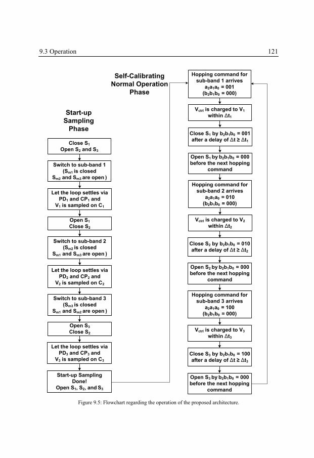
9.3 Operation 121
Start-up
Sampling
Phase
Vctrl is charged to V1
within Δt1
Open S1 by b2b1b0 = 000
before the next hopping
command
Self-Calibrating
Normal Operation
Phase
Hopping command for
sub-band 1 arrives
a2a1a0 = 001
(b2b1b0 = 000)
Close S1 by b2b1b0 = 001
after a delay of Δt ≥ Δt1
Hopping command for
sub-band 2 arrives
a2a1a0 = 010
(b2b1b0 = 000)
Vctrl is charged to V2
within Δt2
Open S2 by b2b1b0 = 000
before the next hopping
command
Close S2 by b2b1b0 = 010
after a delay of Δt ≥ Δt2
Hopping command for
sub-band 3 arrives
a2a1a0 = 100
(b2b1b0 = 000)
Vctrl is charged to V3
within Δt3
Open S3 by b2b1b0 = 000
before the next hopping
command
Close S3 by b2b1b0 = 100
after a delay of Δt ≥ Δt3
Switch to sub-band 1
(Sm1 is closed
Sm2 and Sm3 are open )
Open S1
Close S2
Close S1
Open S2 and S3
Let the loop settles via
PD1 and CP1 and
V1 is sampled on C1
Switch to sub-band 2
(Sm2 is closed
Sm1 and Sm3 are open )
Open S3
Close S2
Let the loop settles via
PD2 and CP2 and
V2 is sampled on C2
Switch to sub-band 3
(Sm3 is closed
Sm1 and Sm2 are open )
Let the loop settles via
PD3 and CP3 and
V3 is sampled on C3
Start-up Sampling
Done!
Open S1, S2, and S3
Figure 9.5: Flowchart regarding the operation of the proposed architecture.
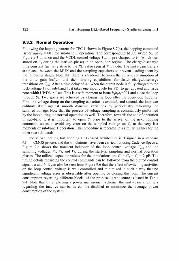
122 Fast Hopping DLL-Based Frequency Synthesis using T/H
9.3.2 Normal Operation
Following the hopping pattern for TFC 1 shown in Figure 8.7(a), the hopping command
issues a2a1a0 = 001 for sub-band 1 operation. The corresponding MUX switch Sm1 in
Figure 9.3 turns on and the VCDL control voltage Vctrl is pre-charged to V1 (which was
stored on C1 during the start-up phase) in an open-loop regime. The charge/discharge
time constant Δt1 is relative to the RC value seen at Vctrl node. The unity-gain buffers
are placed between the MUX and the sampling capacitors to prevent loading them by
the following stages. Note that there is a trade-off between the current consumption of
the unity gain buffers and their driving capabilities for faster charge/discharge
transitions on Vctrl. After a time delay of Δt1 when the output node is fully charged to the
lock-voltage V1 of sub-band 1, it takes one input cycle for PD1 to get updated and issue
zero-width UP/DN pulses. This is a safe moment to issue b2b1b0=001 and close the loop
through S1. Two goals are achieved by closing the loop after the open-loop hopping.
First, the voltage droop on the sampling capacitor is avoided, and second, the loop can
calibrate itself against smooth dynamic variations by periodically refreshing the
sampled voltage. Note that the process of voltage sampling is continuously performed
by the loop during the normal operation as well. Therefore, towards the end of operation
in sub-band 1, it is important to open S1 prior to the arrival of the next hopping
command, so as to avoid any error on the sampled voltage on C1 at the very last
moments of sub-band 1 operation. This procedure is repeated in a similar manner for the
other two sub-bands.
The self-calibrating fast hopping DLL-based architecture is designed in a standard
65-nm CMOS process and the simulations have been carried out using Cadence Spectre.
Figure 9.6 shows the transient behavior of the loop control voltage Vctrl and the
sampling voltages V1, V2, and V3, during the start-up sampling and normal operation
phases. The utilized capacitor values for the simulations are C1 = C2 = C3 = 2 pF. The
timing details regarding the control commands can be followed from the plotted control
signals a and b. It can also be seen from Figure 9.6 that the effect of switching activities
on the loop control voltage is well controlled and minimized in such a way that no
significant voltage error is observable after opening or closing the loop. The current
consumption regarding different blocks of the proposed architecture is listed in Table
9-1. Note that by employing a power management scheme, the unity-gain amplifiers
regarding the inactive sub-bands can be disabled to minimize the average power
consumption of the system.
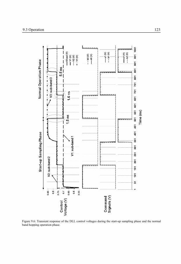
9.3 Operation 123
Figure 9.6: Transient response of the DLL control voltages during the start-up sampling phase and the normal
band hopping operation phase.
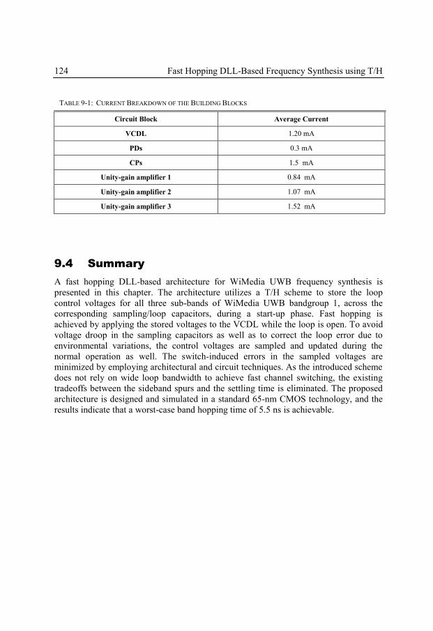
124 Fast Hopping DLL-Based Frequency Synthesis using T/H
9.4 Summary
A fast hopping DLL-based architecture for WiMedia UWB frequency synthesis is
presented in this chapter. The architecture utilizes a T/H scheme to store the loop
control voltages for all three sub-bands of WiMedia UWB bandgroup 1, across the
corresponding sampling/loop capacitors, during a start-up phase. Fast hopping is
achieved by applying the stored voltages to the VCDL while the loop is open. To avoid
voltage droop in the sampling capacitors as well as to correct the loop error due to
environmental variations, the control voltages are sampled and updated during the
normal operation as well. The switch-induced errors in the sampled voltages are
minimized by employing architectural and circuit techniques. As the introduced scheme
does not rely on wide loop bandwidth to achieve fast channel switching, the existing
tradeoffs between the sideband spurs and the settling time is eliminated. The proposed
architecture is designed and simulated in a standard 65-nm CMOS technology, and the
results indicate that a worst-case band hopping time of 5.5 ns is achievable.
TABLE 9-1: CURRENT BREAKDOWN OF THE BUILDING BLOCKS
Circuit Block Average Current
VCDL 1.20 mA
PDs 0.3 mA
CPs 1.5 mA
Unity-gain amplifier 1 0.84 mA
Unity-gain amplifier 2 1.07 mA
Unity-gain amplifier 3 1.52 mA
125
Chapter 10
Low-Power Sub-Harmonic
Upconversion
10.1 Introduction
Handling high-speed wireless data transmission with small power consumption is a key
requirement for many portable applications including UWB technology. Due to
relatively small average transmit power of UWB communications (‒41.25 dBm/MHz),
the requirement on the output power of the power amplifier (PA) is relaxed. Hence, the
total power consumption of the TX is not necessarily dominated by the PA. This implies
that lowering the overall power consumption of TX can be also achieved by minimizing
the power dissipation of the other building blocks through several design choices and
techniques. Since passive mixers do not dissipate any DC power, their power
consumption is mainly limited to the generation of LO signals and buffers. Also, in
contrast to their active counterparts, passive mixers can operate at lower supply
voltages, as the transistor stacking is eliminated. In addition, high performance switches
which are provided by CMOS technologies let the passive mixers take advantage from
technology scaling. Moreover, the LO‒RF feedthrough in passive mixers is less than
that in active mixers [89]. However, poor reverse isolation from RF to baseband (BB) in
passive mixers limits their applications in TX. The low RF‒BB isolation causes
126 Low-Power Sub-Harmonic Upconversion
crosstalk between the I and Q signal paths [90], which transforms the baseband
impedance to the RF side and vice versa, through frequency shifting [91]‒[98]. Shown
in Figure 10.1, to tackle the reverse isolation problem, the outputs of the passive mixers
can be directly shorted if IQ LO signals of 25% duty cycle are applied to the mixer
switches [89], [99], [100]. Doing so, there is only either I or Q path from the BB to RF
at any instant of time. Although this architecture provides smaller power consumption
compared to that of active upconversion mixers, it still requires high performance
frequency synthesizers to provide high carrier frequencies. In addition, it needs to
dissipate quite large amount of power in high frequency LO buffer circuitries to
generate sharp clock edges required for adequate performance of the passive mixers.
This chapter is based on [8] and presents a low-power direct upconversion IQ
modulator for UWB communications, based on multiphase duty-cycled sub-harmonic
passive mixers. The novelty of the architecture is in employing a quadrature mixer array
in such a configuration that the upconversion of the baseband signal can be performed
using a much lower LO frequency, i.e., a sub-harmonic of the carrier. As a result,
several benefits can be gained. Requiring a sub-harmonic LO (SHLO) relaxes the
requirements on the frequency synthesizer circuitry. Moreover, the need for digital
power-hungry or analog inductor-based high frequency LO buffers is alleviated. In
addition, since rail-to-rail LO signals can be provided easier and with less power
consumption at lower frequencies, passive mixers can be employed in the mixer array to
improve the power consumption and linearity of the overall transmitter. Multiphase LO
LO1
LO2
LO3
LO4
LO1 LO2
DAC
BBI+
BBI-
RF+
RF-
LO3 LO4
LO1 LO2
DAC
BBQ+
BBQ-
Figure 10.1: Conventional direct conversion IQ TX with 25% duty cycle passive mixers.
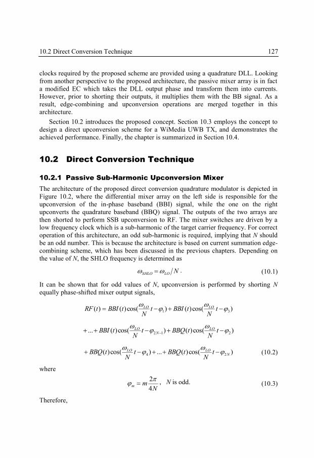
10.2 Direct Conversion Technique 127
clocks required by the proposed scheme are provided using a quadrature DLL. Looking
from another perspective to the proposed architecture, the passive mixer array is in fact
a modified EC which takes the DLL output phase and transform them into currents.
However, prior to shorting their outputs, it multiplies them with the BB signal. As a
result, edge-combining and upconversion operations are merged together in this
architecture.
Section 10.2 introduces the proposed concept. Section 10.3 employs the concept to
design a direct upconversion scheme for a WiMedia UWB TX, and demonstrates the
achieved performance. Finally, the chapter is summarized in Section 10.4.
10.2 Direct Conversion Technique
10.2.1 Passive Sub-Harmonic Upconversion Mixer
The architecture of the proposed direct conversion quadrature modulator is depicted in
Figure 10.2, where the differential mixer array on the left side is responsible for the
upconversion of the in-phase baseband (BBI) signal, while the one on the right
upconverts the quadrature baseband (BBQ) signal. The outputs of the two arrays are
then shorted to perform SSB upconversion to RF. The mixer switches are driven by a
low frequency clock which is a sub-harmonic of the target carrier frequency. For correct
operation of this architecture, an odd sub-harmonic is required, implying that N should
be an odd number. This is because the architecture is based on current summation edge-
combining scheme, which has been discussed in the previous chapters. Depending on
the value of N, the SHLO frequency is determined as
NLOSHLO . (10.1)
It can be shown that for odd values of N, upconversion is performed by shorting N
equally phase-shifted mixer output signals,
)cos()()cos()()( 31
tN
tBBItN
tBBItRF LOLO
)cos()()cos()(... 212
tN
tBBQtN
tBBI LON
LO
)cos()(...)cos()( 24 NLOLO t
NtBBQt
NtBBQ
(10.2)
where
N
mm4
2 , N is odd. (10.3)
Therefore,
128 Low-Power Sub-Harmonic Upconversion
)cos(...)cos()()( 121 N
LOLO tN
tN
tBBItRF
)cos(...)cos()( 22 N
LOLO tN
tN
tBBQ
)2
cos()()cos()(
ttBBQttBBI LOLO. (10.4)
Equation (10.4) can be proved employing the Fourier analysis of the DLL output
phases. In order to eliminate the problem of IQ crosstalk in the upconversion passive
mixers, duty-cycled clock phases are required. As it can be observed in Figure 10.2,
embedded passive AND operations are realized by utilizing two switches in series,
driven by two output phases of the DLL. Those two phases are selected in such a way
that the required duty-cycled pulses are generated. The required pulsewidth k for IQ
isolations is expressed as
N
Tk SHLO
4 (10.5)
where TSHLO is the period of the SHLO clock. Note that there exists a tradeoff between
SHLO frequency and the number of multiphase mixer quads, i.e., circuit complexity.
Ф1
Ф1
Ф2
Ф3
Ф3
Ф2
Ф2N-1
Ф2N-1
Ф2N
Ф1
Ф1
Ф2N
DAC
BBI+
BBI-
BBQ+
BBQ-
RF+ RF
-
DAC
Ф2
Ф1
Ф2
Ф2N
Ф2N-1
Ф2N
Ф2
Ф3
Ф2
Ф2N
Ф2N
Ф1
Multi-Phase IQ
Clock Generation
ωSHLO = ωLO/N
Ф1 Ф2 Ф2N
Figure 10.2: Proposed direct upconversion based on duty-cycled multiphase sub-harmonic passive mixers.
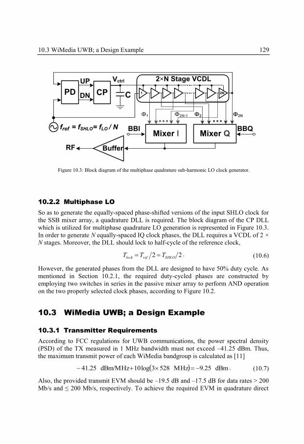
10.3 WiMedia UWB; a Design Example 129
10.2.2 Multiphase LO
So as to generate the equally-spaced phase-shifted versions of the input SHLO clock for
the SSB mixer array, a quadrature DLL is required. The block diagram of the CP DLL
which is utilized for multiphase quadrature LO generation is represented in Figure 10.3.
In order to generate N equally-spaced IQ clock phases, the DLL requires a VCDL of 2 ×
N stages. Moreover, the DLL should lock to half-cycle of the reference clock,
22 SHLOreflock TTT . (10.6)
However, the generated phases from the DLL are designed to have 50% duty cycle. As
mentioned in Section 10.2.1, the required duty-cycled phases are constructed by
employing two switches in series in the passive mixer array to perform AND operation
on the two properly selected clock phases, according to Figure 10.2.
10.3 WiMedia UWB; a Design Example
10.3.1 Transmitter Requirements
According to FCC regulations for UWB communications, the power spectral density
(PSD) of the TX measured in 1 MHz bandwidth must not exceed ‒41.25 dBm. Thus,
the maximum transmit power of each WiMedia bandgroup is calculated as [11]
dBm25.9MHz5283log10dBm/MHz25.41 . (10.7)
Also, the provided transmit EVM should be ‒19.5 dB and ‒17.5 dB for data rates > 200
Mb/s and ≤ 200 Mb/s, respectively. To achieve the required EVM in quadrature direct
PD CP
Mixer Ifref = fSHLO= fLO / N
UP
DN C
RF
1 2N
Mixer QBBQBBI
2×N Stage VCDL
Ф1 Ф2N-1 Ф2 Ф2N
Buffer
Vctrl
Figure 10.3: Block diagram of the multiphase quadrature sub-harmonic LO clock generator.
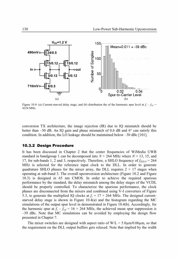
130 Low-Power Sub-Harmonic Upconversion
conversion TX architecture, the image rejection (IR) due to IQ mismatch should be
better than ‒30 dB. An IQ gain and phase mismatch of 0.6 dB and 6° can satisfy this
condition. In addition, the LO leakage should be maintained below ‒30 dBc [101].
10.3.2 Design Procedure
It has been discussed in Chapter 2 that the center frequencies of WiMedia UWB
standard in bandgroup 1 can be decomposed into N × 264 MHz where N = 13, 15, and
17, for sub-bands 1, 2 and 3, respectively. Therefore, a SHLO frequency of fSHLO = 264
MHz is selected for the reference input clock to the DLL. In order to generate
quadrature SHLO phases for the mixer array, the DLL requires 2 × 17 stages when
operating at sub-band 3. The overall upconversion architecture (Figure 10.2 and Figure
10.3) is designed in 65 nm CMOS. In order to achieve the required spurious
performance by the standard, the delay mismatch among the delay stages of the VCDL
should be properly controlled. To characterize the spurious performance, the clock
phases are disconnected from the mixers and combined using V-I converters of Figure
5.3, to generate the multiplied IQ clocks at fc = 17 × 264 MHz. The designed current-
starved delay stage is shown in Figure 10.4(a) and the histogram regarding the MC
simulations of the output spur level in demonstrated in Figure 10.4(b). Accordingly, for
the harmonic spur at fc ‒ fref = 16 × 264 MHz, the achieved mean spur suppression is
‒39 dBc. Note that MC simulations can be avoided by employing the design flow
presented in Chapter 7.
The mixer switches are designed with aspect ratio of W/L = 5.0µm/0.06µm, so that
the requirement on the DLL output buffers gets relaxed. Note that implied by the width
490mV
in
24/0.5
710mV
15/0.12
5/0.12
8/0.5
VDD=1.2 V
out
15/0.12
5/0.12
(a) (b)
Figure 10.4: (a) Current-starved delay stage, and (b) distribution the of the harmonic spur level at fc ‒ fref =
4224 MHz.
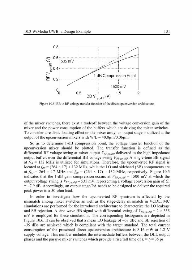
10.3 WiMedia UWB; a Design Example 131
of the mixer switches, there exist a tradeoff between the voltage conversion gain of the
mixer and the power consumption of the buffers which are driving the mixer switches.
To consider a realistic loading effect on the mixer array, an output stage is utilized at the
output of the upconversion mixers with W/L = 40.0µm/0.06µm.
So as to determine 1-dB compression point, the voltage transfer function of the
upconversion mixer should be plotted. The transfer function is defined as the
differential RF voltage swing at mixer output VRF,pp,diff delivered to the high impedance
output buffer, over the differential BB voltage swing VBB,pp,diff. A single-tone BB signal
at fBB = 132 MHz is utilized for simulations. Therefore, the upconverted RF signal is
located at fRF = (264 × 17) + 132 MHz, while the LO and sideband (SB) components are
at fLO = 264 × 17 MHz and fSB = (264 × 17) – 132 MHz, respectively. Figure 10.5
indicates that the 1-dB gain compression occurs at VBB,pp,diff = 1500 mV at which the
output voltage swing is VRF,pp,diff = 535 mV, representing a voltage conversion gain of Gc
= –7.9 dB. Accordingly, an output stage/PA needs to be designed to deliver the required
peak power to a 50-ohm load.
In order to investigate how the upconverted RF spectrum is affected by the
mismatch among mixer switches as well as the stage-delay mismatch in VCDL, MC
simulations are performed for the introduced architecture to characterize the LO leakage
and SB rejection. A sine wave BB signal with differential swing of VBB,pp,diff = 2 × 355
mV is employed for these simulations. The corresponding histograms are depicted in
Figure 10.6. It can be observed that a mean LO leakage of –68 dBc and SB rejection of
–39 dBc are achieved which is compliant with the target standard. The total current
consumption of the presented direct upconversion architecture is 8.16 mW at 1.2 V
supply voltage. This number includes the intermediate buffers between the DLL output
phases and the passive mixer switches which provide a rise/fall time of tr ≈ tf ≈ 35 ps.
Figure 10.5: BB to RF voltage transfer function of the direct upconversion architecture.
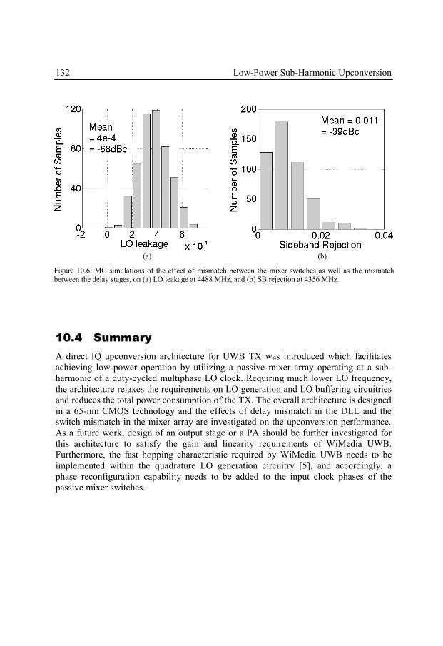
132 Low-Power Sub-Harmonic Upconversion
10.4 Summary
A direct IQ upconversion architecture for UWB TX was introduced which facilitates
achieving low-power operation by utilizing a passive mixer array operating at a sub-
harmonic of a duty-cycled multiphase LO clock. Requiring much lower LO frequency,
the architecture relaxes the requirements on LO generation and LO buffering circuitries
and reduces the total power consumption of the TX. The overall architecture is designed
in a 65-nm CMOS technology and the effects of delay mismatch in the DLL and the
switch mismatch in the mixer array are investigated on the upconversion performance.
As a future work, design of an output stage or a PA should be further investigated for
this architecture to satisfy the gain and linearity requirements of WiMedia UWB.
Furthermore, the fast hopping characteristic required by WiMedia UWB needs to be
implemented within the quadrature LO generation circuitry [5], and accordingly, a
phase reconfiguration capability needs to be added to the input clock phases of the
passive mixer switches.
(a) (b)
Figure 10.6: MC simulations of the effect of mismatch between the mixer switches as well as the mismatch between the delay stages, on (a) LO leakage at 4488 MHz, and (b) SB rejection at 4356 MHz.
133
Chapter 11
Conclusion and Future Work
11.1 Conclusion
The frequency synthesizer is an essential building block in RF transceiver front-ends.
The performance of a synthesizer directly affects the quality of a communication link,
i.e., the SNR in the receiver and EVM in the transmitter side. WiMedia specification for
UWB communication is developed for high speed transmission of large amount of data
in short range wireless applications, such as Wireless USB. It utilizes multiband OFDM
modulation scheme and combines it with the band hopping characteristic of FHSS
systems to realize a wireless link which has a better immunity to interference and
multipath fading effects. Accordingly, the frequency synthesizer must provide a channel
switching speed of less than 9.5 ns, while achieving the sideband spur levels as low as
‒45 dBc. These stringent requirements need to be satisfied at reasonably low power
consumption, as the standard targets portable devices in a WPAN. As a result, the
design of such synthesizers is a challenging task which cannot be achieved using
conventional approaches, and hence, demands further research to develop novel
architectural and circuit techniques.
134 Conclusion and Future Work
Essential characteristics of a DLL, such as its first-order loop stability, relatively wide
loop bandwidth, and low jitter accumulation, indicate its potential as an attractive
solution for fast switching and low phase noise frequency synthesis. On the other hand,
since a DLL only contains a variable of phase, it requires an EC to produce different
frequencies than that of its reference clock. However, misalignment in the equally-
spaced DLL edges will result in harmonic spurs at the output spectrum of the
synthesizer. These harmonic tones downconvert the out-of-band interferers into the
desired channel and corrupt the wanted signals.
This dissertation has addressed the potential of DLL-based architectures for
designing frequency synthesizers for wireless applications, specifically high data rate
UWB communication. Chapters 1 ‒ 4 of the thesis has provided the introduction and
the necessary background to the topic. The main contributions of the thesis have been
covered in Chapters 5 ‒ 10, from which Chapters 5 ‒ 7 focus on the mathematical
analysis for development of behavioral, analytical and prediction models of the spurious
performance in edge-combining DLL-based frequency synthesizers [1], [2]. The
introduced models include the effect of system non-idealities such as the delay
mismatch among the delay stages, the SPE of the loop due to the mismatches between
the up and down signals in PD and CP, and the DCD of the reference clock. The
analysis has provided deep understanding of the harmonic spur behaviors in such
synthesizers. The ultimate goal of the analysis has been to develop closed-form
expressions for robust and accurate prediction of harmonic spur levels of the
synthesizer, which can replace cumbersome statistical simulations in the iterative design
flow of the synthesizer.
Chapters 8 ‒ 10 focus on the design and implementation of novel architectural and
circuit techniques for frequency synthesis using DLL-based approach. The aim has been
to satisfy the challenging requirements of WiMedia UWB communication, while
keeping the power consumption as low as possible. In total, three different architectures
and two calibration techniques have been proposed.
The first architecture is based on a hybrid scheme which employs a fast hopping
edge-combining DLL-based synthesizer along with an injection-locking technique [3],
[6]. Fast hopping is achieved by introducing a compensation technique which cancels
the effect of band switching on the VCDL delay change. A VCDL with variable number
of stages and programmable gain is presented to implement the compensation
technique. An analysis is provided for the relation between the compensation accuracy
and the achieved improvement in the synthesizer’s hopping speed. In order to make the
compensation technique immune to PVT variations, two calibration algorithms are
proposed [4], [5]. The fast hopping characteristic of the proposed DLL-based
synthesizer allows the ILO to employ the remaining time slot for its own settling, while
relaxing the current consumption requirements in the multistage V-I converter of the
EC. The synthesizer has been designed and implemented in a 65-nm CMOS technology
and the measurement is still ongoing at the time of writing the thesis. The preliminary
11.2 Future Work 135
measurement results demonstrate a competitive performance to the state-of-the-art
UWB synthesizers [6].
The second fast hopping DLL-based architecture employs the concept of T/H [7].
During a start-up phase, the lock voltages of the DLL for the three sub-bands of
WiMedia UWB bandgroup 1, are sampled and stored across three corresponding
capacitors. During normal operation when the hopping command arrives, the loop is
pre-charged to the stored voltages in an open-loop regime to achieve fast band
switching. Certain architectural and circuit techniques are utilized so as to minimize the
switch-induced errors in the sampled voltages. This architecture does not rely on the
loop bandwidth of the DLL to achieve fast hopping operation. Therefore, the existing
tradeoff in locked-loop systems between the settling time and the level of the ripples on
the control voltage is eliminated. As a result, the sideband spurs can be suppressed by
employing a larger loop capacitance. Furthermore, since the settling time is detached
from the loop bandwidth, the VCDL can be biased in the low gain regions of its transfer
function to reduce its noise amplification and improve the overall phase noise of the
synthesizer. The architecture is designed in a standard 65-nm CMOS process and the
simulation results verify the achieved band hopping speed of less than 9.5 ns.
The third architecture puts one step forward and merges the edge-combining
operation with the upconversion [8]. This means that instead of combining the phase-
shifted outputs of the DLL to generate the carrier frequency, they are first multiplied
with the analog BB signal from the DAC, and then their outputs are combined in order
to generate the upconverted RF signal. The resulting architecture is a low-power direct
conversion IQ modulator which is based on multiphase duty-cycled sub-harmonic
passive mixers. It employs a quadrature mixer array in such an arrangement that the
upconversion operation can be performed using a sub-harmonic frequency of the
carrier. Generating a low frequency sub-harmonic LO relaxes the requirements on the
design of frequency synthesizer circuitries and LO buffers. Furthermore, rail-to-rail sub-
harmonic LO signals can be generated easier and with smaller power consumption, as
their frequency is much lower than that of the LO signals. The use of the passive mixers
within the mixer array reduces the overall power dissipation and improves the linearity
of the overall transmitter chain.
11.2 Future Work
Estimation of the performance or yield for any complex electronic system which
contains stochastic variables, such as mismatch, requires exhaustive statistical
simulations. This implies that the introduced analysis for deriving the prediction model
of the synthesizer’s spurious performance is not limited to this application and can be
applied to other circuits and systems as a future research. However, it should be noted
that for those systems which contain too many variables and several uncertainty
parameters, deriving closed-form expressions may result in extremely complicated
mathematical derivations. On the other hand, for very simple circuits such as a
136 Conclusion and Future Work
differential amplifier, statistical simulations perform acceptably fast. Therefore, for both
of these two cases, statistical simulation will outperform mathematical derivations.
According to the presented analysis of the harmonic spurs in edge-combining DLL-
based frequency synthesizers, the sideband spur levels are highly dependent on the
stage-delay mismatch of the delay line. It has also been discussed that in order to reduce
the standard deviation of the delay mismatch, large-area devices need to be employed in
the delay stage. This results in area and speed penalties. Another potential research topic
can be the investigation and development of specific calibration techniques which can
compensate the stage-delay deviations, and therefore, relax the requirements on the
device areas for a given spurious performance.
The synthesizer architecture of [7] exhibits the potential for improving the hopping
speed, phase noise, and harmonic spurs of the synthesizer at the same time.
Implementing this architecture on silicon and verifying the achievable performance
from the measurement results can also be considered as a valuable future work.
Another opportunity for future research is to further develop the proposed direct
upconversion technique of [8] by including an output stage or a PA in order to realize a
complete low-power transmitter solution for WiMedia UWB. In addition, the ability to
hop between different sub-bands needs be included within the architecture.
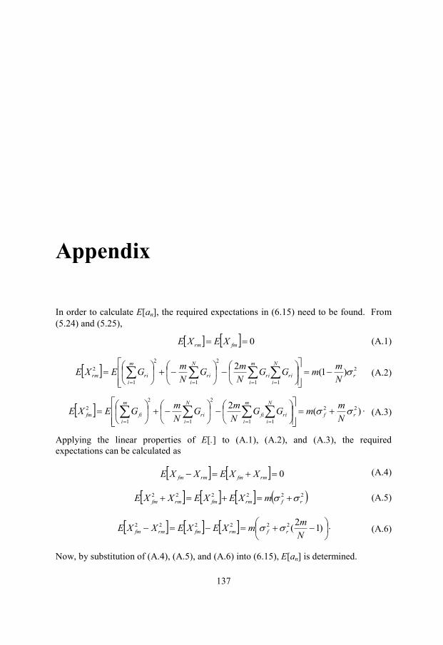
137
Appendix
In order to calculate E[an], the required expectations in (6.15) need to be found. From
(5.24) and (5.25),
0 fmrm XEXE (A.1)
2
1 1
2
1
2
1
2 )1(2
r
m
i
N
i
riri
N
i
ri
m
i
rirmN
mmGG
N
mG
N
mGEXE
(A.2)
)(2 22
1 1
2
1
2
1
2
rf
m
i
N
i
rifi
N
i
ri
m
i
fifmN
mmGG
N
mG
N
mGEXE
. (A.3)
Applying the linear properties of E[.] to (A.1), (A.2), and (A.3), the required
expectations can be calculated as
0 rmfmrmfm XXEXXE (A.4)
222222
rfrmfmrmfm mXEXEXXE (A.5)
)1
2(222222
N
mmXEXEXXE rfrmfmrmfm . (A.6)
Now, by substitution of (A.4), (A.5), and (A.6) into (6.15), E[an] is determined.
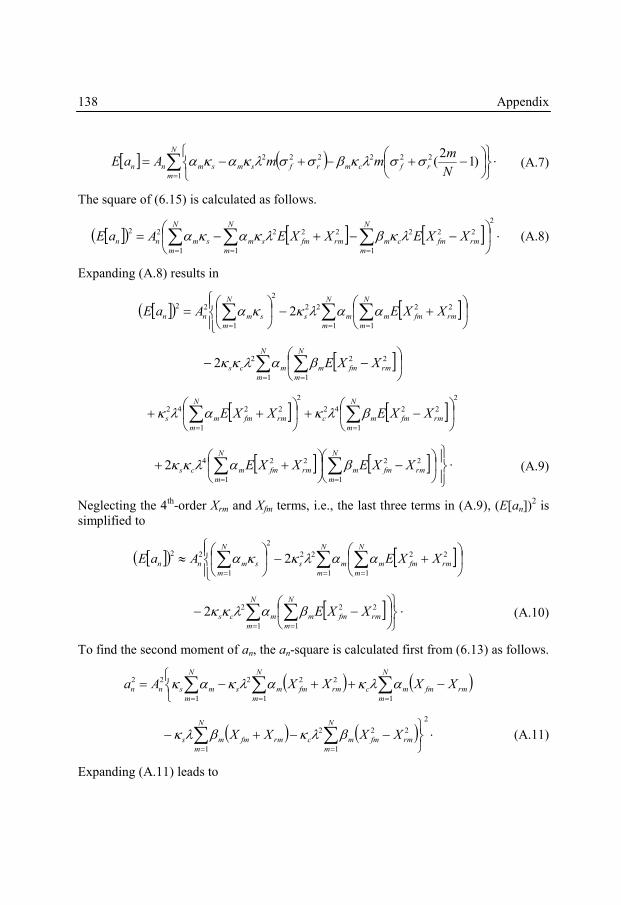
138 Appendix
)12
(222
1
222
N
mmmAaE rfcm
N
m
rfsmsmnn . (A.7)
The square of (6.15) is calculated as follows.
2
1
222
1
222
1
22
N
m
rmfmcm
N
m
rmfmsm
N
m
smnn XXEXXEAaE . (A.8)
Expanding (A.8) results in
N
m
N
m
rmfmmms
N
m
smnn XXEAaE1 1
2222
2
1
222
N
m
N
m
rmfmmmcs XXE1 1
2222
2
1
2242
2
1
2242
N
m
rmfmmc
N
m
rmfmms XXEXXE
N
m
rmfmm
N
m
rmfmmcs XXEXXE1
22
1
2242 . (A.9)
Neglecting the 4th
-order Xrm and Xfm terms, i.e., the last three terms in (A.9), (E[an])2 is
simplified to
N
m
N
m
rmfmmms
N
m
smnn XXEAaE1 1
2222
2
1
222
N
m
N
m
rmfmmmcs XXE1 1
2222 . (A.10)
To find the second moment of an, the an-square is calculated first from (6.13) as follows.
N
m
rmfmmc
N
m
rmfmms
N
m
msnn XXXXAa11
222
1
22
2
1
222
1
N
m
rmfmmc
N
m
rmfmms XXXX . (A.11)
Expanding (A.11) leads to
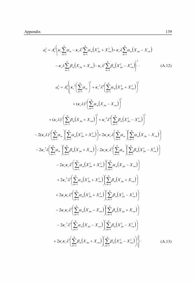
Appendix 139
N
m
rmfmmc
N
m
rmfmms
N
m
msnn XXXXAa11
222
1
22
2
1
222
1
N
m
rmfmmc
N
m
rmfmms XXXX . (A.12)
2
1
2242
2
1
222N
m
rmfmms
N
m
msnn XXAa
2
1
2)(
N
m
rmfmmc XX
2
1
2242
2
1
2)(
N
m
rmfmmc
N
m
rmfmms XXXX
N
m
rmfmm
N
m
mcs
N
m
rmfmm
N
m
ms XXXX111
22
1
2 2)(2
N
m
rmfmm
N
m
mcs
N
m
rmfmm
N
m
ms XXXX1
22
1
2
11
222
N
m
rmfmm
N
m
rmfmmcs XXXX11
2232
N
m
rmfmm
N
m
rmfmms XXXX11
22322
N
m
rmfmm
N
m
rmfmmcs XXXX1
22
1
2242
N
m
rmfmm
N
m
rmfmmcs XXXX11
22
N
m
rmfmm
N
m
rmfmmc XXXX1
22
1
322
N
m
rmfmm
N
m
rmfmmcs XXXX1
22
1
32 . (A.13)
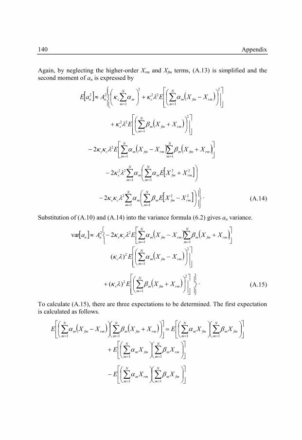
140 Appendix
Again, by neglecting the higher-order Xrm and Xfm terms, (A.13) is simplified and the
second moment of an is expressed by
2
1
22
2
1
22N
m
rmfmmc
N
m
msnn XXEAaE
2
1
22N
m
rmfmms XXE
N
m
rmfmm
N
m
rmfmmcs XXXXE11
22
N
m
rmfmm
N
m
ms XXE1
22
1
222
N
m
rmfmm
N
m
mcs XXE1
22
1
22 . (A.14)
Substitution of (A.10) and (A.14) into the variance formula (6.2) gives an variance.
N
m
rmfmm
N
m
rmfmmcsnn XXXXEAa11
22 2var
2
1
2)(N
m
rmfmmc XXE
2
1
2)(N
m
rmfmms XXE . (A.15)
To calculate (A.15), there are three expectations to be determined. The first expectation
is calculated as follows.
N
m
fmm
N
m
fmm
N
m
rmfmm
N
m
rmfmm XXEXXXXE1111
N
m
rmm
N
m
fmm XXE11
N
m
fmm
N
m
rmm XXE11
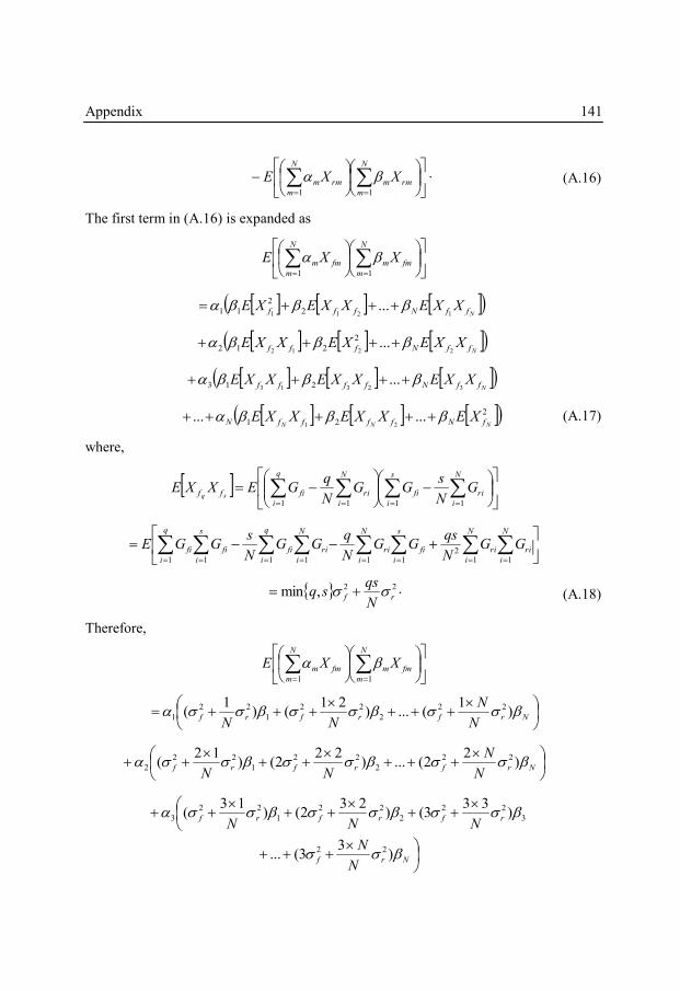
Appendix 141
N
m
rmm
N
m
rmm XXE11
. (A.16)
The first term in (A.16) is expanded as
N
m
fmm
N
m
fmm XXE11
NffNfff XXEXXEXE
1211...2
2
11
NffNfff XXEXEXXE
2212...2
212
NffNffff XXEXXEXXE
32313...213
2
21 ......21 NNN fNffffN XEXXEXXE (A.17)
where,
N
i
ri
s
i
fi
N
i
ri
q
i
fiff GN
sGG
N
qGEXXE
sq
1111
N
i
ri
N
i
ri
s
i
fi
N
i
ri
q
i
s
i
q
i
N
i
rifififi GGN
qsGG
N
qGG
N
sGGE
112
111 1 1 1
22,min rfN
qssq . (A.18)
Therefore,
N
m
fmm
N
m
fmm XXE11
Nrfrfrf
N
N
NN )
1(...)
21()
1( 22
2
22
1
22
1
Nrfrfrf
N
N
NN )
22(...)
222()
12( 22
2
22
1
22
2
3
22
2
22
1
22
3 )33
3()23
2()13
( rfrfrfNNN
Nrf
N
N )
33(... 22
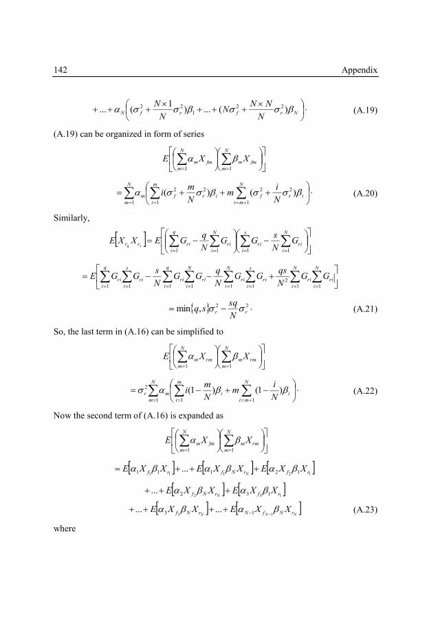
142 Appendix
NrfrfN
N
NNN
N
N )(...)
1(... 22
1
22 . (A.19)
(A.19) can be organized in form of series
N
m
fmm
N
m
fmm XXE11
N
m
N
mi
irf
m
i
irfmN
im
N
mi
1 1
22
1
22 )()( . (A.20)
Similarly,
N
i
ri
s
i
ri
N
i
ri
q
i
rirr GN
sGG
N
qGEXXE
sq
1111
N
i
ri
N
i
ri
s
i
ri
N
i
ri
q
i
s
i
q
i
N
i
riririri GGN
qsGG
N
qGG
N
sGGE
112
111 1 1 1
22,min rrN
sqsq . (A.21)
So, the last term in (A.16) can be simplified to
N
m
rmm
N
m
rmm XXE11
N
m
N
mi
i
m
i
imrN
im
N
mi
1 11
2 )1()1( . (A.22)
Now the second term of (A.16) is expanded as
N
m
rmm
N
m
fmm XXE11
12111 12111 ... rfrNfrf XXEXXEXXE
N
132 132... rfrNf XXEXXE
N
NNN rNfNrNf XXEXXE
13 13 ...... (A.23)
where
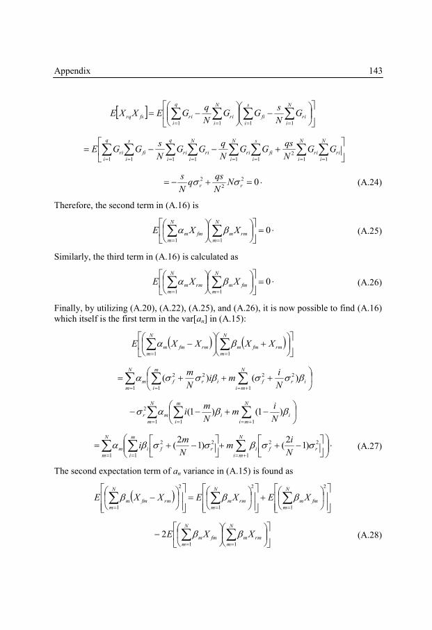
Appendix 143
N
i
ri
s
i
fi
N
i
ri
q
i
rifsrq GN
sGG
N
qGEXXE
1111
N
i
ri
N
i
ri
s
i
fi
N
i
ri
q
i
s
i
q
i
N
i
ririfiri GGN
qsGG
N
qGG
N
sGGE
112
111 1 1 1
02
2
2 rr NN
qsq
N
s . (A.24)
Therefore, the second term in (A.16) is
011
N
m
rmm
N
m
fmm XXE . (A.25)
Similarly, the third term in (A.16) is calculated as
011
N
m
fmm
N
m
rmm XXE . (A.26)
Finally, by utilizing (A.20), (A.22), (A.25), and (A.26), it is now possible to find (A.16)
which itself is the first term in the var[an] in (A.15):
N
m
rmfmm
N
m
rmfmm XXXXE11
N
m
N
mi
irf
m
i
irfmN
imi
N
m
1 1
22
1
22 )()(
N
m
N
mi
i
m
i
imrN
im
N
mi
1 11
2 )1()1(
N
mi
rfi
m
i
rfi
N
m
mN
im
N
mi
1
22
1
22
1
)12
()12
( . (A.27)
The second expectation term of an variance in (A.15) is found as
2
1
2
1
2
1
N
m
fmm
N
m
rmm
N
m
rmfmm XEXEXXE
N
m
rmm
N
m
fmm XXE11
2 (A.28)
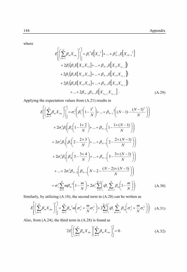
144 Appendix
where
2
1
2
1
2
1
2
1
2
1
...
rNNr
N
m
rmm XEXEXE
1112121 ...2
NrrNrr XXEXXE
1213232 ...2
NrrNrr XXEXXE
1314343 ...2
NrrNrr XXEXXE
12122...
NN rrNN XXE . (A.29)
Applying the expectation values from (A.21) results in
N
NN
NXE Nr
N
m
rmm
22
1
22
1
2
2
1
)1()1(...
11
N
N
NNr
)1(11...
2112 121
2
N
N
NNr
)1(22...
3222 132
2
N
N
NNr
)1(33...
4332 143
2
N
NNNNNr
)1()2(22... 12
2
1
1 1
2
1
22 121N
i
N
im
mir
N
m
mrN
mi
N
mm . (A.30)
Similarly, by utilizing (A.18), the second term in (A.28) can be written as
1
1 1
22
1
222
2
1
2N
i
N
im
rfmi
N
m
rfm
N
m
fmmN
mi
N
mmXE . (A.31)
Also, from (A.24), the third term in (A.28) is found as
0211
N
m
rmm
N
m
fmm XXE . (A.32)
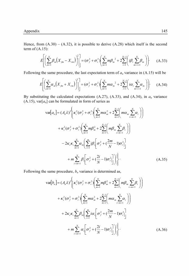
Appendix 145
Hence, from (A.30) ‒ (A.32), it is possible to derive (A.28) which itself is the second
term of (A.15):
1
1 11
222
2
1
2)(N
i
N
im
mi
N
m
mrf
N
m
rmfmm imXXE . (A.33)
Following the same procedure, the last expectation term of an variance in (A.15) will be
1
1 11
222
2
1
2)(N
i
N
im
mi
N
m
mrf
N
m
rmfmm imXXE . (A.34)
By substituting the calculated expectations (A.27), (A.33), and (A.34), in an variance
(A.15), var[an] can be formulated in form of series as
1
1 11
22222 2)()(varN
m
N
mi
im
N
m
mrfcnn mmAa
1
1 11
2222 2)(N
m
N
mi
im
N
m
mrfs mm
m
i
rfi
N
m
mcsN
mi
1
22
1
)12
(2
N
mi
rfiN
im
1
22 )12
( . (A.35)
Following the same procedure, bn variance is determined as,
1
1 11
22222 2)()(varN
m
N
mi
im
N
m
mrfcnn mmAb
1
1 11
2222 2)(N
m
N
mi
im
N
m
mrfs mm
m
i
rfi
N
m
mcsN
mi
1
22
1
)12
(2
N
mi
rfiN
im
1
22 )12
( . (A.36)

146 Appendix
147
References
[1] A. Ojani, B. Mesgarzadeh, and A. Alvandpour, “Modeling and analysis of
harmonic spurs in DLL-based frequency synthesizers,” IEEE Transactions on
Circuits and Systems I: Regular Papers, vol. PP, no. 99, pp. 1–10, Jun. 2014.
[2] A. Ojani, B. Mesgarzadeh, and A. Alvandpour, “Monte Carlo-free prediction of
spurious performance for ECDLL-based synthesizers,” IEEE Transactions on
Circuits and Systems I: Regular Papers, Accepted for Publication, Aug. 2014,
DOI: 10.1109/TCSI.2014.2347231.
[3] A. Ojani, B. Mesgarzadeh, and A. Alvandpour, “A DLL-based injection-locked
frequency synthesizer for WiMedia UWB,” IEEE International Symposium on
Circuits and Systems (ISCAS), Seoul, South Korea, May 2012, pp. 2027–2030.
[4] A. Ojani, B. Mesgarzadeh, and A. Alvandpour, “A process variation tolerant
DLL-based UWB frequency synthesizer,” 55th IEEE International Midwest
Symposium on Circuits and Systems (MWSCAS), Boise, ID, USA, Aug. 2012, pp.
558–561.
[5] A. Ojani, B. Mesgarzadeh, and A. Alvandpour, “A quadrature UWB frequency
synthesizer with dynamic settling-time calibration,” IEEE International
Symposium on Circuits and Systems (ISCAS), Beijing, China, May 2013, pp.
2480–2483.
148 References
[6] A. Ojani, B. Mesgarzadeh, and A. Alvandpour, “A 65-nm CMOS UWB
frequency synthesizer,” Manuscript to be Submitted for Publication.
[7] A. Ojani, B. Mesgarzadeh, and A. Alvandpour, “A self-calibration technique for
fast-switching frequency-hopped UWB synthesis,” 21th IEEE International
Conference Mixed Design of Integrated Circuits and Systems (MIXDES), Lublin,
Poland, Jun. 2014, pp. 154–159.
[8] A. Ojani, B. Mesgarzadeh, and A. Alvandpour, “A low-power direct IQ
upconversion technique based on duty-cycled multi-phase sub-harmonic passive
mixers for UWB transmitters,” IEEE International Symposium on Integrated
Circuits (ISIC), Singapore, Dec. 2014.
[9] G. Heidari, WiMedia UWB Technology of Choice for Wireless USB and
Bluetooth. UK: Wiley, 2008.
[10] High rate ultra wideband PHY and MAC standard, ECMA-368, Dec. 2008, 3rd
ed. http://www.ecma-international.org/publications/standards/Ecma-368.htm.
[11] K. Iniewski, Wireless Technologies: Circuits, Systems, and Devices. New York:
CRC, 2007.
[12] F. Gardner, Phaselock Techniques, 3rd ed. New Jersey: Wiley Inter-Science,
2005.
[13] N. Lanka, S. Patnaik, and R. Harjani, “Frequency-hopped quadrature frequency
synthesizer in 0.13-µm technology,” IEEE Journal of Solid-State Circuits, vol.
46, pp. 2021–2032, Sept. 2011.
[14] G. Tak, S. Hyun, T. Kang, B. Choi, and S. Park, “A 6.3–9 GHz fast settling PLL
for MB-OFDM UWB applications,” IEEE Journal of Solid-State Circuits, vol.
40, pp. 1671–1679, Aug. 2005.
[15] D. Leenaerts, R. Beek, J. Bergervoet, H. Kundur, G. Weide, A. Kapoor, T. Pu, Y.
Fang, Y. Wang, B. Mukkada, H. Lim, V. Kiran, C. Lim, S. Badiu, and A. Chang,
“A 65 nm CMOS Inductorless triple band group WiMedia UWB PHY,” IEEE
Journal of Solid-State Circuits, vol. 44, pp. 3499–3510, Dec. 2009.
[16] B. Razavi, T. Aytur, F. Yang, R. Yan, H. Kang, C. Hsu, and C. Lee, “A 0.13 μm
CMOS UWB transceiver,” IEEE International Solid-State Circuits Conference,
vol. 48, Feb. 2005, pp. 216–217.
References 149
[17] T. Aytur, H. Kang, R. Mahadevappa, M. Altintas, S. Brink, T. Diep, C. Hsu, F.
Shi, F. Yang, C. Lee, R. Yan, and B. Razavi, “A fully integrated UWB PHY in
0.13 µm CMOS,” IEEE International Solid-State Circuits Conference, Feb. 2006,
pp. 124–125.
[18] Y. Zheng, Y. Tong, C. Ang, Y. Xu, W. Yeoh, F. Lin, and R. Singh, “A CMOS
carrier-less UWB transceiver for WPAN applications,” IEEE International Solid-
State Circuits Conference, vol. 49, Feb. 2006, pp. 116–117.
[19] D. Leenaerts, R. Beek, G. Weide, K. Harish, H. Wiate, Y. Zhang, C. Razzell, and
R. Roovers, “A SiGe BiCMOS 1ns fast hopping frequency synthesizer for UWB
radio,” IEEE International Solid-State Circuits Conference, vol. 48, Feb. 2005,
pp. 202–203.
[20] H. Chae, E. Park, and C. Cha, “A fast hopping frequency synthesizer for UWB
systems in a CMOS technology,” International Symposium on Wireless
Communication Systems, Sept. 2005, pp. 370–374.
[21] J. Lee, E. Park, C. Cha, H. Chae, C. Suh, J. Koh, H. Lee, and H. Kim, “A
frequency synthesizer for UWB transceiver in 0.13 μm CMOS technology,”
Silicon Monolithic Integrated Circuits in RF systems, pp. 294–297, Jan. 2006.
[22] J. Lee and D. Chiu, “A 7-band 3 to 8 GHz frequency synthesizer with 1ns band-
switching time in 0.18 μm CMOS technology,” IEEE International Solid-State
Circuits Conference, vol. 48, Feb. 2005, pp. 204–205.
[23] J. Lee, “A 3-to-8-GHz fast-hopping frequency synthesizer in 0.18 μm CMOS
technology,” IEEE Journal of Solid-State Circuits, vol. 41, pp. 566–573, Mar.
2006.
[24] C. Lin and C. Wang, “A semi-dynamic regenerative frequency divider for mode-1
MB-OFDM UWB hopping carrier generation,” IEEE International Solid-State
Circuits Conference, vol. 48, Feb. 2005, pp. 206–207.
[25] R. Beek, D. Leenaerts, and G. Weide, “A fast-hopping single-PLL 3-band UWB
synthesizer in 0.25 μm SiGe BiCMOS,” IEEE European Solid-State Circuit
Conference, Sept. 2005, pp. 173–176.
[26] S. Toso, A. Bevilacqua, M. Tiebout, S. Marsili, C. Sandner, A. Gerosa, and A.
Neviani, “UWB fast-hopping frequency generation based on sub-harmonic
injection locking,” IEEE Journal of Solid-State Circuits, vol. 43, pp. 2844–2852,
Dec. 2008.
150 References
[27] M. Izad and C. Hng, “A pulse shaping technique for spur suppression in
Injection-locked synthesizers,” IEEE Journal of Solid State Circuits, vol. 47, pp.
652–664, Mar. 2012.
[28] B. Razavi, “Challenges in the design of frequency synthesizers for wireless
applications,” IEEE Custom Integrated Circuits Conference, May 1997, pp. 395–
402.
[29] C. Sandner, S. Derksen, D. Draxelmayr, S. Ek, V. Filimon, G. Leach, S. Marsli,
D. Matveev, K. Mertens, F. Micli, H. Paule, M. Punzenberger, C. Reindl, R.
Salerno, M. Tiebout, A. Wiesbauer, I. Winter, and Z. Zhang, “A
WiMedia/MBOA-compliant CMOS RF transceiver for UWB,” IEEE
International Solid-State Circuits Conference, vol. 49, Feb. 2006, pp. 122–123.
[30] B. Razavi, Phase-locking in high-performance systems: from devices to
architectures. Wiley-IEEE Press, 2003.
[31] M. Bazes, “A novel precision MOS synchronous delay line,” IEEE Journal of
Solid-State Circuits, vol. 20, pp. 1265–1271, Dec. 1985.
[32] M. Johnson, E. Hudson, “A variable delay line PLL for CPU-coprocessor
synchronization,” IEEE Journal of Solid-State Circuits, vol. 23, pp. 1218–1223,
Oct. 1988.
[33] D. Messerschmitt, “Synchronization in digital system design,” IEEE Journal of
Selected Areas in Communications, vol. 8, pp. 1404–1419, Oct. 1990.
[34] T. Lee, K. Donnelly, J. Ho, J. Zerbe, M. Johnson, and T. Ishikawa, “A 2.5 V
CMOS delay-locked loop for 18 Mbit, 500 megabyte/s DRAM,” IEEE Journal of
Solid-State Circuits, vol. 29, pp. 1491–1496, Dec. 1994.
[35] T. Lee and K. Hsiao, “The design and analysis of a DLL-based frequency
synthesizer for UWB application,” IEEE Journal of Solid-State Circuits, vol. 41,
pp. 1245–1252, Jun. 2006.
[36] G. Chien and P. Gray, “A 900-MHz local oscillator using a DLL-based frequency
multiplier technique for PCS applications,” IEEE Journal of Solid-State Circuits,
vol. 35, pp. 1996–1999, Dec. 2000.
[37] B. Razavi, RF Microelectronics, 2nd ed. New York: Prentice Hall, 2012.
References 151
[38] Y. Jung, S. Lee, D. Shim, W. Kim, C. Kim, and S. Cho, “A low jitter dual loop
DLL using multiple VCDLs with a duty cycle corrector,” IEEE Symposium on
VLSI Circuits, Jun. 2000, pp. 50–51.
[39] Y. Jung, S. Lee, D. Shim, W. Kim, C. Kim, and S. Cho, “A dual-loop delay-
locked loop using multiple voltage-controlled delay lines,” IEEE Journal of
Solid-State Circuits, vol. 36, pp. 784–791, May 2001.
[40] C. Jeong, C. Yoo, J. Lee, and J. Kih, “Digital delay locked loop with open-loop
digital duty cycle corrector for 1.2 Gb/s/pin double data rate SDRAM,” IEEE
European Solid-State Circuits Conference, Sept. 2004, pp. 379–384.
[41] D. Shin, J. Song, H. Chae, and C. Kim, “A 7 ps Jitter 0.053 mm2 Fast Lock All-
Digital DLL With a Wide Range and High Resolution DCC,” IEEE Journal of
Solid-State Circuits, vol.44, pp. 2437–2451, Sept. 2009.
[42] D. Shin, K. Na, D. Kwon, J. Kang, T. Song, H. Jung, W. Lee, K. Park, J. Park, Y.
Joo, J. Cha, Y. Jung, Y. Kim, D. Han, B. Choi, G. Lee, J. Cho, and Y. Choi,
“Wide-range fast-lock duty-cycle corrector with offset-tolerant duty-cycle
detection scheme for 54nm 7Gb/s GDDR5 DRAM interface,” IEEE Symposium
on VLSI Circuits, Jun. 2009, pp. 138‒139.
[43] R. Mehta, S. Seth, S. Shashidharan, B. Chattopadhyay, and S. Chakravarty, “A
programmable, multi-GHz, wide-range duty cycle correction circuit in 45nm
CMOS process,” IEEE European Solid-State Circuit Conference, Sept. 2012, pp.
257–260.
[44] S. Bae, J. Seo, H. Yeo, J. Kim, J. Sim, and H. Park, “An all-digital 90-degree
phase-shift DLL with loop-embedded DCC for 1.6Gbps DDR interface,” IEEE
Custom Integrated Circuits Conference, Sept. 2007, pp. 373–376.
[45] B. Kim, K. Oh, L. Kim, and D. Lee, “A 500MHz DLL with second order duty
cycle corrector for low jitter,” IEEE Custom Integrated Circuits Conference,
Sept. 2005, pp. 325–328.
[46] S. Kao and S. Liu, “All-digital fast-locked synchronous duty-cycle corrector,”
IEEE Transactions on Circuits and Systems II: Express Briefs, vol. 53, pp. 1363–
1367, Dec. 2006.
[47] K. Cheng, C. Su, and K. Chang, “A high linearity, fast-locking pulsewidth control
loop with digitally programmable duty cycle correction for wide range
operation,” IEEE Journal of Solid-State Circuits, vol. 43, Feb. 2008, pp. 399–
413.
152 References
[48] Y. Wang, S. Kao, and S. Liu, “All-digital delay-locked loop/pulsewidth-control
loop with adjustable duty cycles,” IEEE Journal of Solid-State Circuits, vol. 41,
pp. 1262–1274, Jun. 2006.
[49] S. Han and S. Liu, “A 500-MHz‒1.25-GHz fast-locking pulsewidth control loop
with presettable duty cycle,” IEEE Journal of Solid-State Circuits, vol.39, pp.
463–468, Mar. 2004.
[50] S. Han and S. Liu, “A single-path pulsewidth control loop with a built-in delay-
locked loop,” IEEE Journal of Solid-State Circuits, vol. 40, pp. 1130–1135, May
2005.
[51] C. Liang, S. Chen, and S. Liu, “A digital calibration technique for charge pumps
in phase-locked systems,” IEEE Journal of Solid-State Circuits, vol. 43, pp. 390–
398, Feb. 2008.
[52] D. Rennie and M. Sachdev, “A 5-Gb/s CDR circuit with automatically calibrated
linear phase detector,” IEEE Transactions on Circuits and Systems I: Regular
Papers, vol. 55, pp. 796–803, Apr. 2008.
[53] C. Chuang and S. Liu, “A 0.5-5-GHz wide-range multiphase DLL with a
calibrated charge pump,” IEEE Transactions on Circuits and Systems II: Express
Briefs, vol. 54, pp. 939–943, Nov. 2007.
[54] P. Maulik and D. Mercer, “A DLL-based programmable clock multiplier in
0.18μm CMOS with ‒70 dBc reference spur,” IEEE Journal of Solid-State
Circuits, vol. 42, pp. 1642–1648, Aug. 2007.
[55] G. Marucci, A. Fenaroli, G. Marzin, S. Levantino, C. Samori, and A. Lacaita, “A
1.7 GHz MDLL-based fractional-N frequency synthesizer with 1.4ps RMS
integrated jitter and 3mW power using 1b TDC,” IEEE International Solid-State
Circuits Conference, Feb. 2014, pp. 360–361.
[56] A. Elshazly, R. Inti, B. Young, and P. Hanumolu, “A 1.5GHz 890uW digital
MDLL with 400fsrms integrated jitter, –55.6dBc reference spur and 20fs/mV
supply-noise sensitivity using 1b TDC,” IEEE International Solid-State Circuits
Conference, Feb. 2012, pp. 242–244.
[57] T. Ali, A. Hafez, R. Drost, R. Ho, and C. Yang, “A 4.6GHz MDLL with ‒46dBc
reference spur and aperture position tuning,” IEEE International Solid-State
Circuits Conference, Feb. 2011, pp. 466–467.
References 153
[58] B. Helal, M. Straayer, G. Wei, and M. Perrott, “A highly digital MDLL-based
clock multiplier that leverages a self-scrambling time-to-digital converter to
achieve subpicosecond jitter performance,” IEEE Journal of Solid-State
Circuits, vol. 43, pp. 855–863, Apr. 2008.
[59] S. Gierkink, “An 800 MHz –122 dBc/Hz-at-200 kHz clock multiplier based on a
combination of PLL and recirculating DLL,” IEEE International Solid-State
Circuits Conference, Feb. 2008, pp. 454–455.
[60] S. Gierkink, “Low-spur, low-phase-noise clock multiplier based on a combination
of PLL and recirculating DLL with dual-pulse ring oscillator and self-correcting
charge pump,” IEEE Journal of Solid-State Circuits, vol. 43, pp. 2967–2976,
Dec. 2008.
[61] G. Marzin, A. Fenaroli, G. Marucci, S. Levantino, C. Samori, and A. Lacaita, “A
spur cancellation technique for MDLL-based frequency synthesizers,” IEEE
International Symposium Circuits and Systems, May 2013, pp. 165–168.
[62] J. Zhuang, Q. Du, and T. Kwasniewski, “A –107 dBc 10 kHz carrier offset 2-GHz
DLL-based frequency synthesizer,” IEEE Custom Integrated Circuits
Conference, Sept. 2003, pp. 301–304.
[63] J. Zhuang, Q. Du, and T. Kwasniewski, “Noise, spur characteristics and in-lock
error reduction of DLL-based frequency synthesizers,” International Conference
on Communications, Circuits and Systems, Jun. 2004, pp. 1443–1446.
[64] O. Casha, I. Grech, F. Badets, D. Morche, and J. Micallef, “Analysis of the spur
characteristics of edge-combining DLL-based frequency multipliers,” IEEE
Transactions on Circuits and Systems II: Express Briefs, vol. 56, pp. 132–136,
Feb. 2009.
[65] N. Khan, M. Hossain, and K. Law, “A low power frequency synthesizer for 60-
GHz wireless personal area networks,” IEEE Transactions on Circuits and
Systems II: Express Briefs, vol.58, pp. 622–626, Oct. 2011.
[66] H. Ng, A. Fischer, R. Feger, R. Stuhlberger, L. Maurer, and A. Stelzer, “A DLL-
supported, low phase noise fractional-N PLL with a wideband VCO and a highly
linear frequency ramp generator for FMCW radars,” IEEE Transactions on
Circuits and Systems I: Regular Papers, vol. 60, pp. 3289–3302, Dec. 2013.
[67] T. Lee and K. Hsiao, “A DLL-based frequency multiplier for MBOA-UWB
system,” IEEE Symposium on VLSI Circuits, Jun. 2005, pp. 42–45.
154 References
[68] M. Pelgrom, A. Duinmaijer, and A. Welbers, “Matching properties of MOS
transistors,” IEEE Journal of Solid-State Circuits, vol. 24, pp. 1433–1440, Oct.
1989.
[69] M. Pelgrom, H. Tuinhout, and M. Vertregt, “Transistor matching in analog
CMOS applications,” IEEE International Electron Device Meeting, Dec. 1998,
pp. 915–918.
[70] K. Lakshmikumar, R. Hadaway, and M. Copeland, “Characterization and
modeling of mismatch in MOS transistors for precision analog design,” IEEE
Journal of Solid-State Circuits, vol. 21, pp. 1057–1066, Dec. 1986.
[71] T. Mizuno, J. Okamura, and A. Toriumi, “Experimental study of threshold
voltage fluctuation due to statistical variation of channel dopant number in
MOSFETs,” IEEE Transactions on Electron Devices, vol. 41, pp. 2216–2221,
Nov. 1994.
[72] J. Shyu, G. Temes, and K. Yao, “Random errors in MOS capacitors,” IEEE
Journal of Solid-State Circuits, vol. 24, pp. 1070–1076, Dec. 1989.
[73] J. Shyu, G. Temes, and F. Krummenacher, “Random errors effects in matched
MOS capacitors and current sources,” IEEE Journal of Solid-State Circuits, vol.
19, pp. 948–956, Dec. 1984.
[74] F. Forti, M. Wright, “Measurement of current mismatch in the weak inversion
region,” IEEE Journal of Solid-State Circuits, vol. 29, pp. 138–142, Feb. 1994.
[75] J. Proakis, and M. Salehi, Digital Communications, 5th ed. New York: McGraw
Hill, 2008.
[76] B. Rivet, L. Girin and C. Jutten, “Log-Rayleigh distribution: a simple and
efficient statistical representation of Log-spectral coefficients,” IEEE
Transactions on Audio, Speech, and Language Processing, vol. 15, pp. 796–802,
Mar. 2007.
[77] J. Maneatis, “Low-Jitter Process-Independent DLL and PLL Based on Self-
Biased Techniques,” IEEE Journal of Solid-State Circuits, vol. 31, pp. 1723–
1732, Nov. 1996.
[78] R. Adler, “A study of locking phenomena in oscillators,” IRE, vol. 6, Jun. 1946,
pp. 351–357.
References 155
[79] B. Razavi, “A study of injection locking and pulling in oscillators,” IEEE Journal
of Solid-State Circuits, vol. 39, pp. 1415–1424, Sept. 2004.
[80] L. Paciorek, “Injection locking of oscillators,” IEEE, Nov. 1965, pp. 1723–1727.
[81] N. Lanka, S. Patnaik, and R. Harjani, “Understanding the Transient Behavior of
Injection Locked LC Oscillators,” IEEE Custom Integrated Circuits Conference,
Sept. 2007, pp. 667–670.
[82] B. Mesgarzadeh and A. Alvandpour, “First-harmonic injection-locked ring
oscillators,” IEEE Custom Integrated Circuits Conference, Sept. 2006, pp. 733–
736.
[83] A. Hastings, The Art of Analog Layout. 2nd ed. New Jersey: Prentice Hall, 2005.
[84] T. Lin and Y. Lai, “An agile VCO frequency calibration technique for a 10-GHz
CMOS PLL,” IEEE Journal of Solid-State Circuits, vol. 42, pp. 340–349, Feb.
2007.
[85] S. Pellerano, R. Mukhopadhyay, A. Ravi, J. Laskar, and Y. Palaskas, “A 39.1-to-
41.6 GHz ΔΣ fractional-N frequency synthesizer in 90 nm CMOS,” IEEE
International Solid-State Circuits Conference, Feb. 2009, pp. 484–485.
[86] J. Lee and B. Razavi, “A 40-Gb/s clock and data recovery circuit in 0.18-µm
CMOS technology,” IEEE Journal of Solid-State Circuits, vol. 38, pp. 2181–
2190, Dec. 2003.
[87] C. Fayomi and G. Roberts, “Design and characterization of low-voltage analog
switch without the need for clock boosting,” IEEE International Midwest
Symposium on Circuits and systems, Jul. 2004, pp. 315–318.
[88] W. Rhee, “Design of high-performance CMOS charge pumps in phase locked
loops,” IEEE International Symposium on Circuits and Systems, May 1999, pp.
545–548.
[89] X. He and J. Sinderen, “A low-power, low-EVM, SAW-less WCDMA
transmitter using direct quadrature voltage modulation,” IEEE Journal of Solid-
State Circuits, vol. 44, pp. 3448–3458, Dec. 2009.
[90] A. Mirzaei, D. Murphy, and H. Darabi, “Analysis of direct-conversion IQ
transmitters with 25% duty-cycle passive mixers,” IEEE Transactions on Circuits
and Systems I: Regular Papers, vol. 58, pp. 2318–2331, Oct. 2011.
156 References
[91] B. Cook, A. Berny, A. Molnar, S. Lanzisera, and K. Pister, “Low-power 2.4-GHz
transceiver with passive RX front-end and 400-mV supply,” IEEE Journal of
Solid-State Circuits, vol. 41, pp. 2757–2766, Dec. 2006.
[92] A. Qualkadi, M. Kaamouchi, J. Paillot, D. Janvier, and D. Flandre, “Fully
integrated high-Q switched capacitor bandpass filter with center frequency and
bandwidth tuning,” IEEE Symposium on Radio Frequency Integrated Circuits,
Jun. 2007, pp. 681–684.
[93] A. Mirzaei, H. Darabi, J. Leete, X. Chen, K. Juan, and A. Yazdi, “Analysis and
optimization of current-driven passive mixers in narrowband direct-conversion
receivers,” IEEE Journal of Solid-State Circuits, vol. 44, pp. 2678–2688, Oct.
2009.
[94] A. Mirzaei, H. Darabi, J. Leete, and Y. Chang, “Analysis and optimization of
direct-conversion receivers with 25% duty-cycle current-driven passive mixers,”
IEEE Transactions on Circuits and Systems I: Regular Papers, vol. 57, pp. 2353–
2366, Sept. 2010.
[95] C. Andrews and A. Molnar, “Implications of passive mixer transparency for
impedance matching and noise figure in passive mixer-first receivers,” IEEE
Transactions on Circuits and Systems I: Regular Papers, vol. 57, pp. 3092–3103,
Dec. 2010.
[96] H. Khatri, P. Gudem, and L. Larson, “A SAW-less CMOS CDMA receiver with
active TX filtering,” IEEE Custom Integrated Circuits Conference, Sept. 2009,
pp. 379–382.
[97] A. Ghaffari, E. Klumperink, and B. Nauta, “A differential 4-path highly linear
widely tunable on-chip bandpass filter,” IEEE Symposium on Radio Frequency
Integrated Circuits, May 2010, pp. 299–302.
[98] N. Kim, L. Larson, and V. Aparin, “A highly linear SAW-less CMOS receiver
using a mixer with embedded TX filtering for CDMA,” IEEE Journal of Solid-
State Circuits, vol. 44, pp. 2126–2135, Aug. 2009.
[99] X. He, J. Sinderen, and R. Rutten, “A 45 nm WCDMA transmitter using direct
quadrature voltage modulator with high oversampling digital front-end,” IEEE
International Solid-State Circuits Conference, Feb. 2010, pp. 62–63.
[100] X. He and J. Sinderen, “A 45 nm low-power SAW-less WCDMA transmit
modulator using direct quadrature voltage modulation,” IEEE International Solid-
State Circuits Conference, Feb. 2009, pp. 120–121.
References 157
[101] B. Razavi, T. Aytur, C. lam, F. Yang, K. Li, R. Yan, H. Kang, C. Hsu, and C.
Lee, “A UWB CMOS transceiver,” IEEE Journal of Solid-State Circuits, vol. 40,
pp. 2555–2562, Dec. 2005.