Embed Size (px)
Citation preview
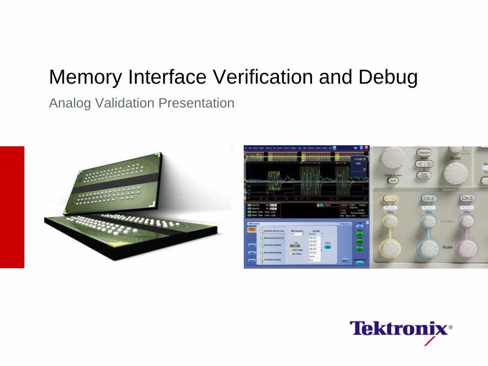
Memory Interface Verification and Debug Analog Validation Presentation
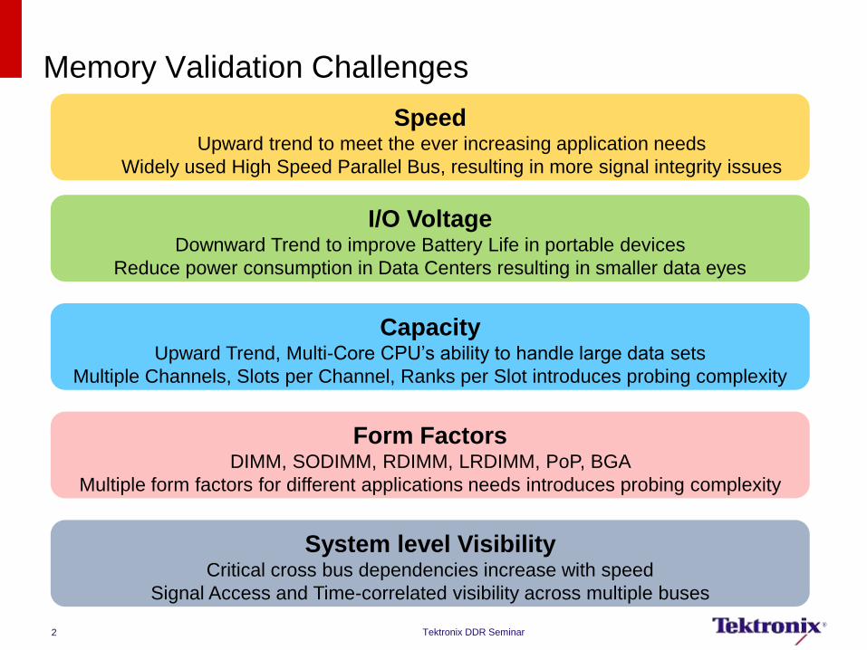
Memory Validation Challenges
Speed Upward trend to meet the ever increasing application needs
Widely used High Speed Parallel Bus, resulting in more signal integrity issues
I/O Voltage Downward Trend to improve Battery Life in portable devices
Reduce power consumption in Data Centers resulting in smaller data eyes
Form Factors DIMM, SODIMM, RDIMM, LRDIMM, PoP, BGA
Multiple form factors for different applications needs introduces probing complexity
System level Visibility Critical cross bus dependencies increase with speed
Signal Access and Time-correlated visibility across multiple buses
Capacity Upward Trend, Multi-Core CPU’s ability to handle large data sets
Multiple Channels, Slots per Channel, Ranks per Slot introduces probing complexity
Tektronix DDR Seminar 2
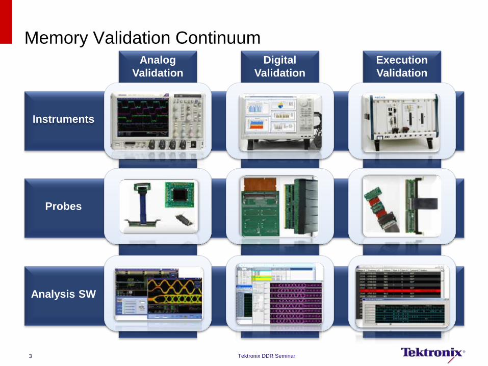
Memory Validation Continuum
Analysis SW
Analog
Validation
Instruments
Probes
3
Digital
Validation
Execution
Validation
Tektronix DDR Seminar
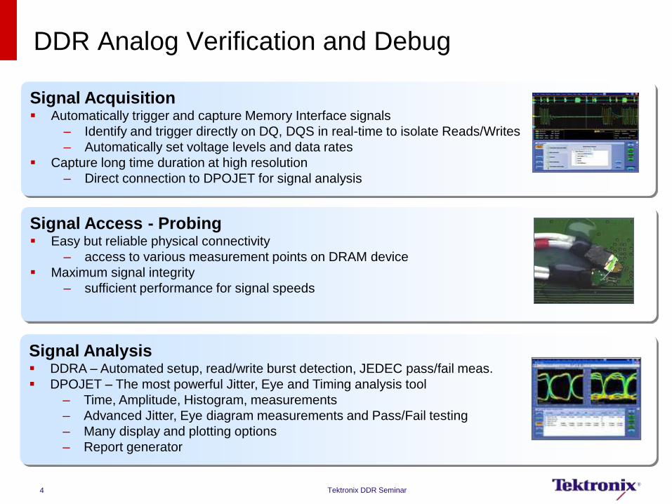
DDR Analog Verification and Debug
Signal Access - Probing Easy but reliable physical connectivity
‒ access to various measurement points on DRAM device
Maximum signal integrity
‒ sufficient performance for signal speeds
Signal Acquisition Automatically trigger and capture Memory Interface signals
‒ Identify and trigger directly on DQ, DQS in real-time to isolate Reads/Writes
‒ Automatically set voltage levels and data rates
Capture long time duration at high resolution
‒ Direct connection to DPOJET for signal analysis
Signal Analysis DDRA – Automated setup, read/write burst detection, JEDEC pass/fail meas.
DPOJET – The most powerful Jitter, Eye and Timing analysis tool
‒ Time, Amplitude, Histogram, measurements
‒ Advanced Jitter, Eye diagram measurements and Pass/Fail testing
‒ Many display and plotting options
‒ Report generator
4 Tektronix DDR Seminar
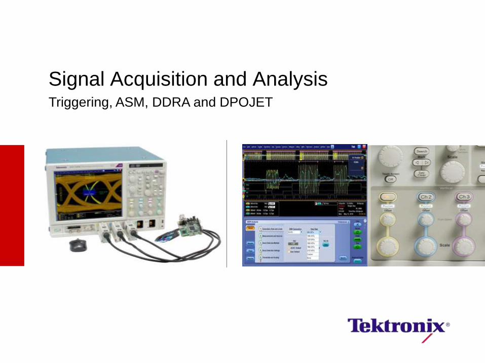
Signal Acquisition and Analysis Triggering, ASM, DDRA and DPOJET
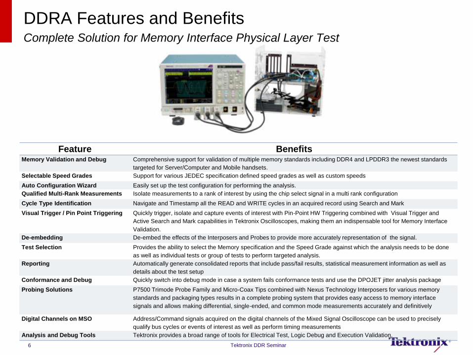
Feature Benefits Memory Validation and Debug Comprehensive support for validation of multiple memory standards including DDR4 and LPDDR3 the newest standards
targeted for Server/Computer and Mobile handsets.
Selectable Speed Grades Support for various JEDEC specification defined speed grades as well as custom speeds
Auto Configuration Wizard Easily set up the test configuration for performing the analysis.
Qualified Multi-Rank Measurements Isolate measurements to a rank of interest by using the chip select signal in a multi rank configuration
Cycle Type Identification Navigate and Timestamp all the READ and WRITE cycles in an acquired record using Search and Mark
Visual Trigger / Pin Point Triggering
Quickly trigger, isolate and capture events of interest with Pin-Point HW Triggering combined with Visual Trigger and
Active Search and Mark capabilities in Tektronix Oscilloscopes, making them an indispensable tool for Memory Interface
Validation.
De-embedding De-embed the effects of the Interposers and Probes to provide more accurately representation of the signal.
Test Selection Provides the ability to select the Memory specification and the Speed Grade against which the analysis needs to be done
as well as individual tests or group of tests to perform targeted analysis.
Reporting Automatically generate consolidated reports that include pass/fail results, statistical measurement information as well as
details about the test setup
Conformance and Debug Quickly switch into debug mode in case a system fails conformance tests and use the DPOJET jitter analysis package
Probing Solutions
P7500 Trimode Probe Family and Micro-Coax Tips combined with Nexus Technology Interposers for various memory
standards and packaging types results in a complete probing system that provides easy access to memory interface
signals and allows making differential, single-ended, and common mode measurements accurately and definitively
Digital Channels on MSO
Address/Command signals acquired on the digital channels of the Mixed Signal Oscilloscope can be used to precisely
qualify bus cycles or events of interest as well as perform timing measurements
Analysis and Debug Tools Tektronix provides a broad range of tools for Electrical Test, Logic Debug and Execution Validation.
DDRA Features and Benefits Complete Solution for Memory Interface Physical Layer Test
6 Tektronix DDR Seminar
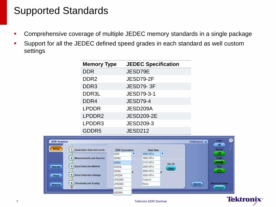
Supported Standards Comprehensive coverage of multiple JEDEC memory standards in a single package
Support for all the JEDEC defined speed grades in each standard as well custom
settings
Memory Type JEDEC Specification
DDR JESD79E
DDR2 JESD79-2F
DDR3 JESD79- 3F
DDR3L JESD79-3-1
DDR4 JESD79-4
LPDDR JESD209A
LPDDR2 JESD209-2E
LPDDR3 JESD209-3
GDDR5 JESD212
7 Tektronix DDR Seminar
www.tektronix.com/ddr
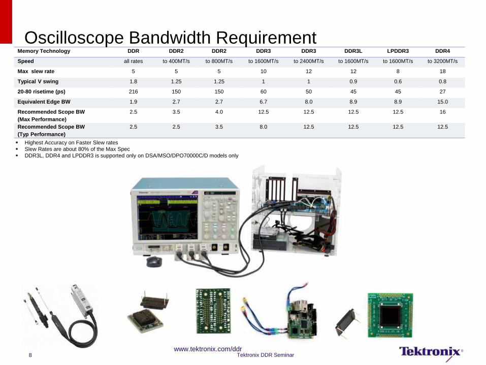
Memory Technology DDR DDR2 DDR2 DDR3 DDR3 DDR3L LPDDR3 DDR4
Speed all rates to 400MT/s to 800MT/s to 1600MT/s to 2400MT/s to 1600MT/s to 1600MT/s to 3200MT/s
Max slew rate 5 5 5 10 12 12 8 18
Typical V swing 1.8 1.25 1.25 1 1 0.9 0.6 0.8
20-80 risetime (ps) 216 150 150 60 50 45 45 27
Equivalent Edge BW 1.9 2.7 2.7 6.7 8.0 8.9 8.9 15.0
Recommended Scope BW
(Max Performance)
2.5 3.5 4.0 12.5 12.5 12.5 12.5 16
Recommended Scope BW
(Typ Performance)
2.5 2.5 3.5 8.0 12.5 12.5 12.5 12.5
Highest Accuracy on Faster Slew rates
Slew Rates are about 80% of the Max Spec
DDR3L, DDR4 and LPDDR3 is supported only on DSA/MSO/DPO70000C/D models only
Oscilloscope Bandwidth Requirement
8 Tektronix DDR Seminar
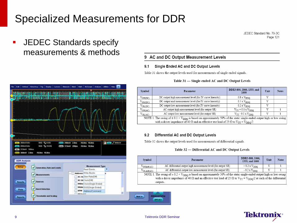
JEDEC Standards specify
measurements & methods
Specialized Measurements for DDR
9 Tektronix DDR Seminar

Test Setup and Configuration
All the tests are logically grouped based on the input source requirement
– READ
– WRITE
– CLOCK
– ADDR/CMD
Quickly set up the test configuration by selecting a complete group or individual tests
for targeted analysis.
Flexible input source requirement, inputs are not hardwired to a particular Oscilloscope
channel.
10 Tektronix DDR Seminar
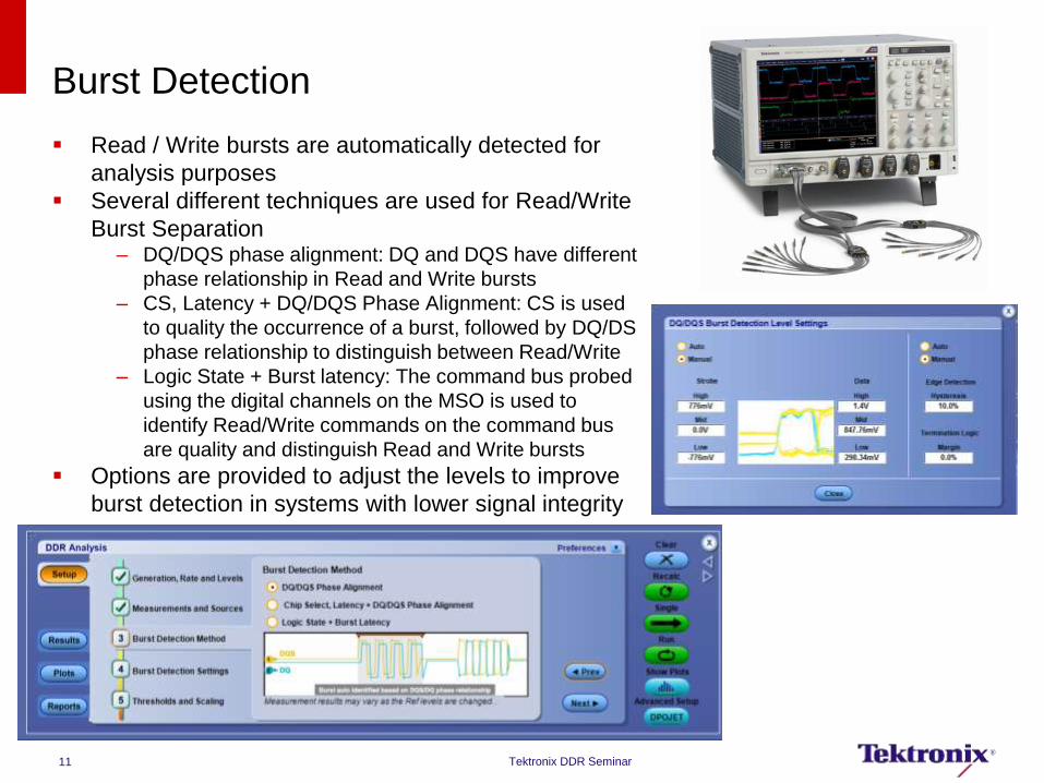
Burst Detection
Read / Write bursts are automatically detected for
analysis purposes
Several different techniques are used for Read/Write
Burst Separation – DQ/DQS phase alignment: DQ and DQS have different
phase relationship in Read and Write bursts
– CS, Latency + DQ/DQS Phase Alignment: CS is used
to quality the occurrence of a burst, followed by DQ/DS
phase relationship to distinguish between Read/Write
– Logic State + Burst latency: The command bus probed
using the digital channels on the MSO is used to
identify Read/Write commands on the command bus
are quality and distinguish Read and Write bursts
Options are provided to adjust the levels to improve
burst detection in systems with lower signal integrity
11 Tektronix DDR Seminar
12
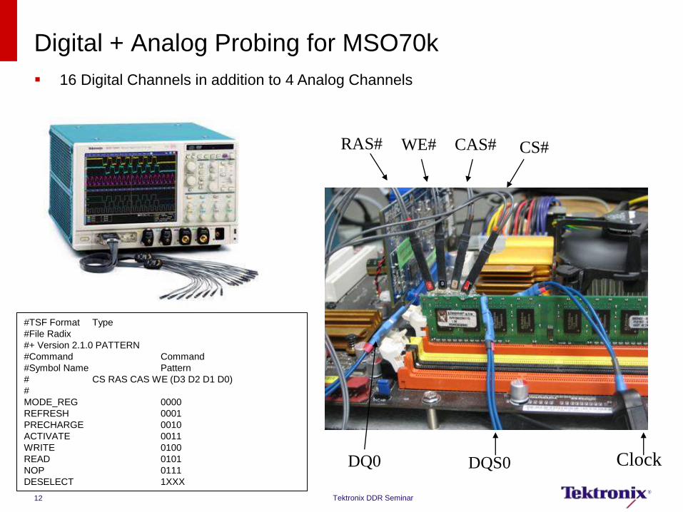
#TSF Format Type
#File Radix
#+ Version 2.1.0 PATTERN
#Command Command
#Symbol Name Pattern
# CS RAS CAS WE (D3 D2 D1 D0)
#
MODE_REG 0000
REFRESH 0001
PRECHARGE 0010
ACTIVATE 0011
WRITE 0100
READ 0101
NOP 0111
DESELECT 1XXX
Digital + Analog Probing for MSO70k
Clock DQS0 DQ0
RAS# WE# CAS# CS#
16 Digital Channels in addition to 4 Analog Channels
Tektronix DDR Seminar
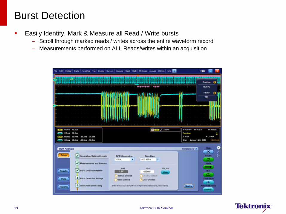
Burst Detection
Easily Identify, Mark & Measure all Read / Write bursts
– Scroll through marked reads / writes across the entire waveform record
– Measurements performed on ALL Reads/writes within an acquisition
13 Tektronix DDR Seminar
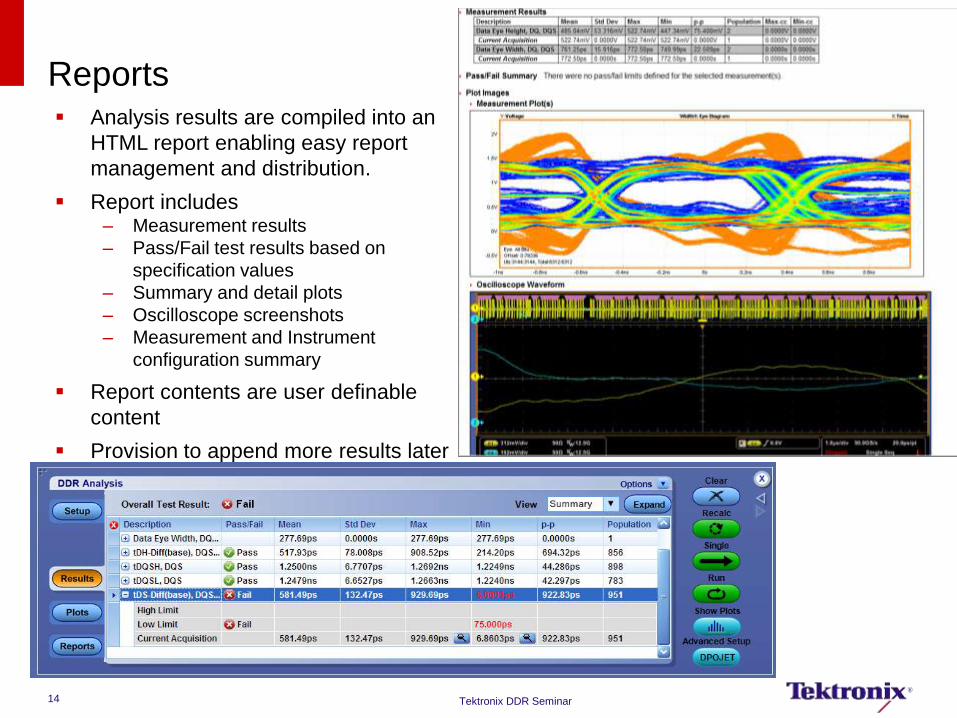
Reports Analysis results are compiled into an
HTML report enabling easy report
management and distribution.
Report includes – Measurement results
– Pass/Fail test results based on
specification values
– Summary and detail plots
– Oscilloscope screenshots
– Measurement and Instrument
configuration summary
Report contents are user definable
content
Provision to append more results later
Tektronix DDR Seminar 14

Beyond DDRA
Tektronix Oscilloscopes come with several tools
that aid in debug of Memory Interfaces
– DPOJET advanced Jitter analysis toolkit
– PinPoint Triggering
– Visual Trigger
– Mask Testing
– Advanced Search and Mark
15 Tektronix DDR Seminar
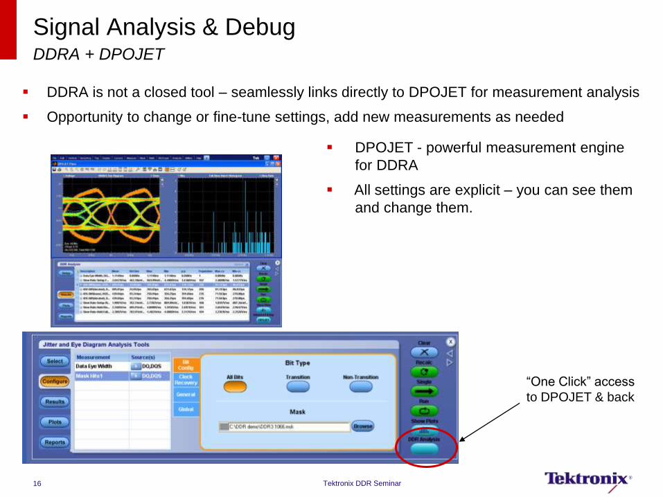
Signal Analysis & Debug DDRA + DPOJET
DDRA is not a closed tool – seamlessly links directly to DPOJET for measurement analysis
Opportunity to change or fine-tune settings, add new measurements as needed
“One Click” access
to DPOJET & back
DPOJET - powerful measurement engine
for DDRA
All settings are explicit – you can see them
and change them.
16 Tektronix DDR Seminar

17
DPOJET Debug Tools
“Find Worst Case Events” feature – Zoom to waveform from Min / Max for each measurement
Tektronix DDR Seminar
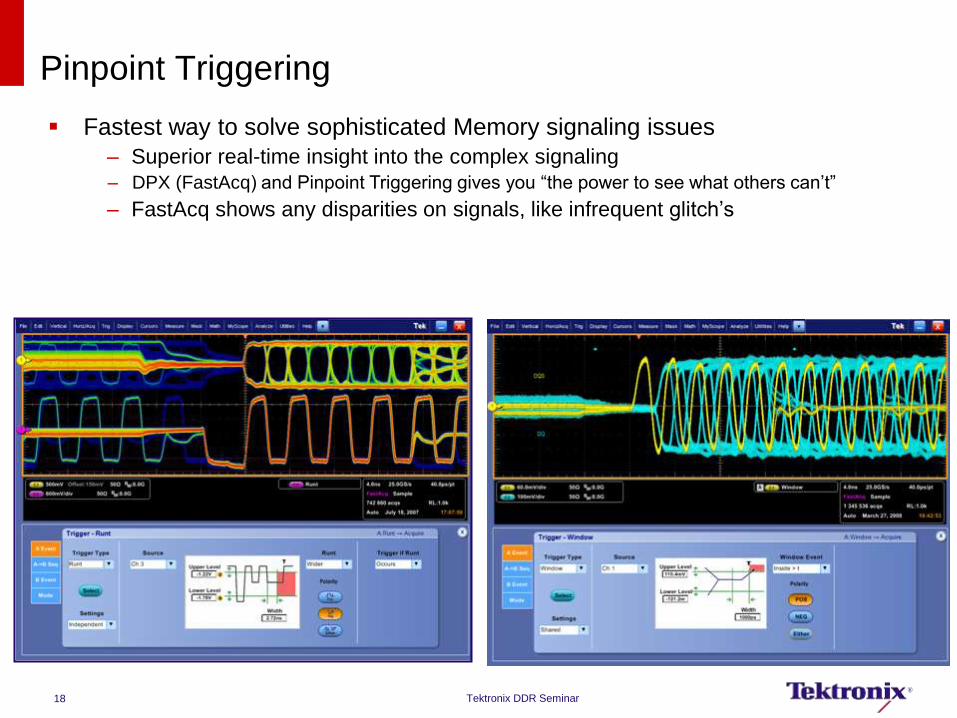
Pinpoint Triggering
Fastest way to solve sophisticated Memory signaling issues
– Superior real-time insight into the complex signaling
– DPX (FastAcq) and Pinpoint Triggering gives you “the power to see what others can’t”
– FastAcq shows any disparities on signals, like infrequent glitch’s
18 Tektronix DDR Seminar
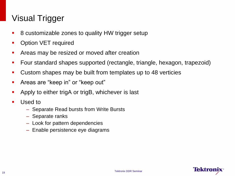
Visual Trigger
8 customizable zones to quality HW trigger setup
Option VET required
Areas may be resized or moved after creation
Four standard shapes supported (rectangle, triangle, hexagon, trapezoid)
Custom shapes may be built from templates up to 48 verticies
Areas are “keep in” or “keep out”
Apply to either trigA or trigB, whichever is last
Used to
– Separate Read bursts from Write Bursts
– Separate ranks
– Look for pattern dependencies
– Enable persistence eye diagrams
19 Tektronix DDR Seminar
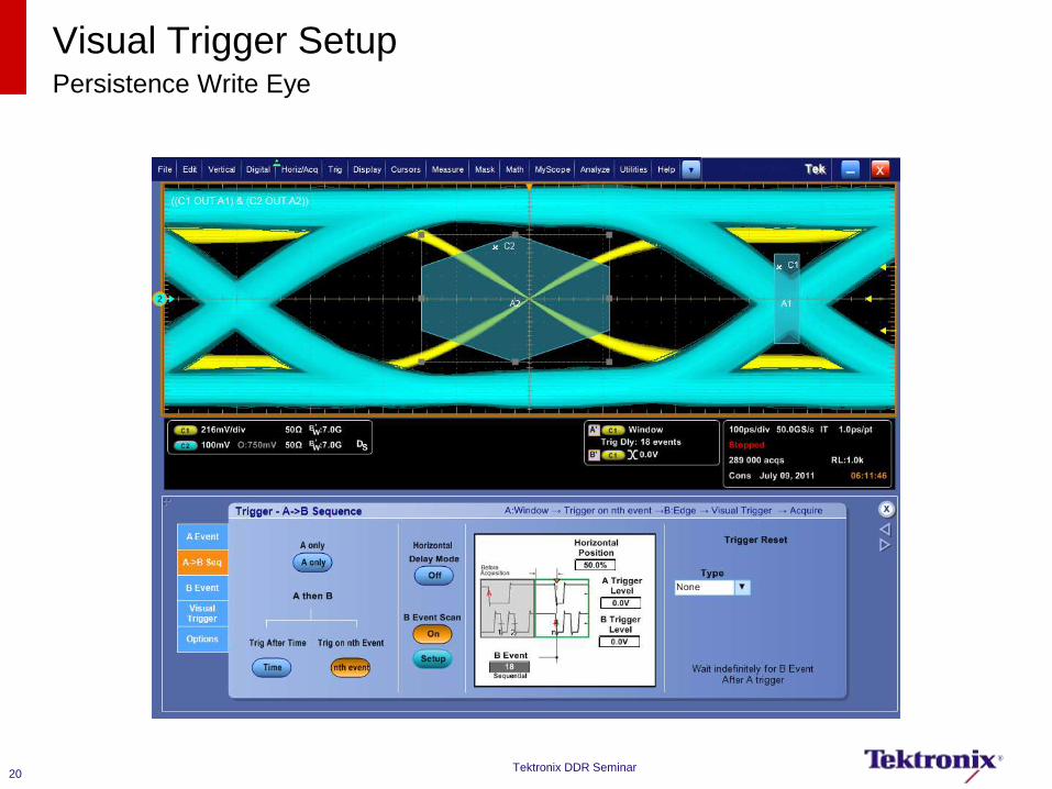
Visual Trigger Setup Persistence Write Eye
20 Tektronix DDR Seminar
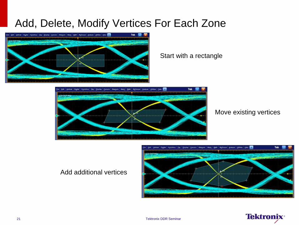
Add, Delete, Modify Vertices For Each Zone
Start with a rectangle
Move existing vertices
Add additional vertices
21 Tektronix DDR Seminar
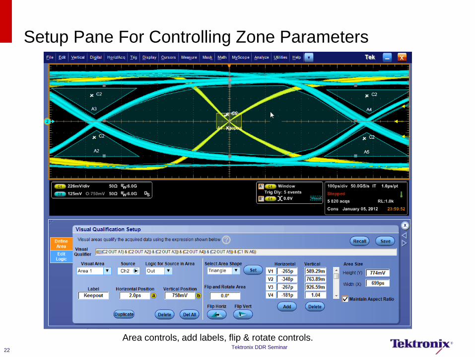
Setup Pane For Controlling Zone Parameters
Area controls, add labels, flip & rotate controls.
22 Tektronix DDR Seminar
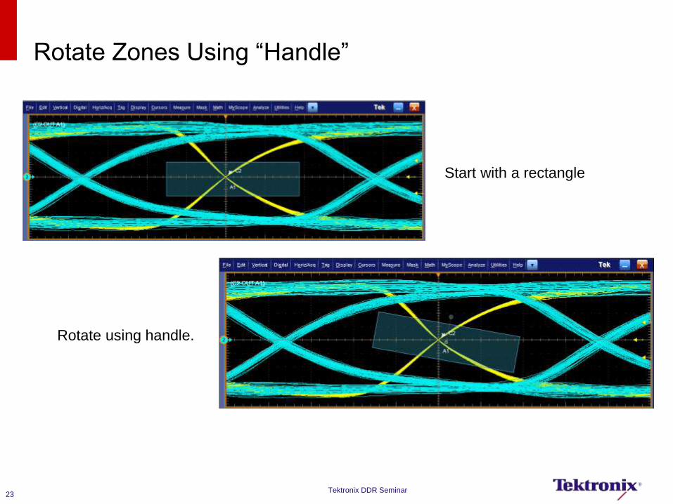
Rotate Zones Using “Handle”
Start with a rectangle
Rotate using handle.
23 Tektronix DDR Seminar
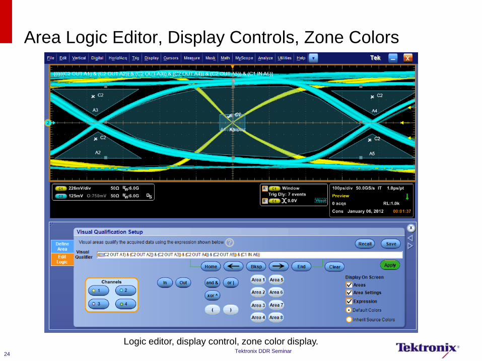
Area Logic Editor, Display Controls, Zone Colors
Logic editor, display control, zone color display.
24 Tektronix DDR Seminar
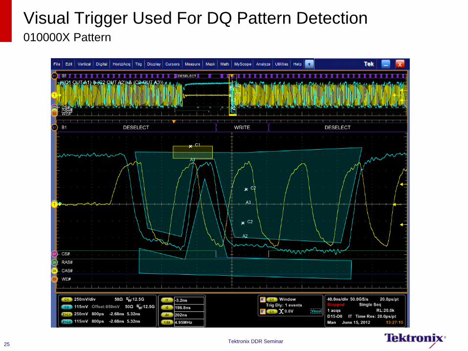
Visual Trigger Used For DQ Pattern Detection 010000X Pattern
25 Tektronix DDR Seminar

Eye Mask testing DRAM Input RX Mask
For DDR4 JEDEC is moving to a
mask based approach for DQ eye
measurement at Rx input
After the Eye is built using DDRA
Using the built in Mask
Measurement capability the
Pass/Fail results can be obtained.
26
Mask = 136mV x 125ps (0.2UI)
Tektronix DDR Seminar
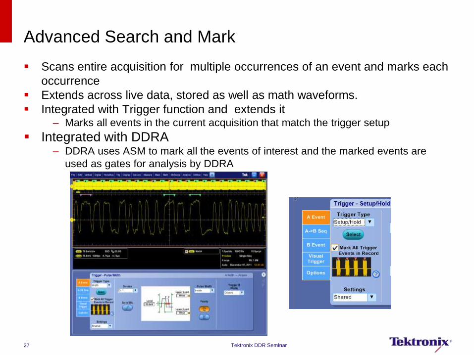
Advanced Search and Mark
Scans entire acquisition for multiple occurrences of an event and marks each
occurrence
Extends across live data, stored as well as math waveforms.
Integrated with Trigger function and extends it – Marks all events in the current acquisition that match the trigger setup
Integrated with DDRA – DDRA uses ASM to mark all the events of interest and the marked events are
used as gates for analysis by DDRA
27 Tektronix DDR Seminar
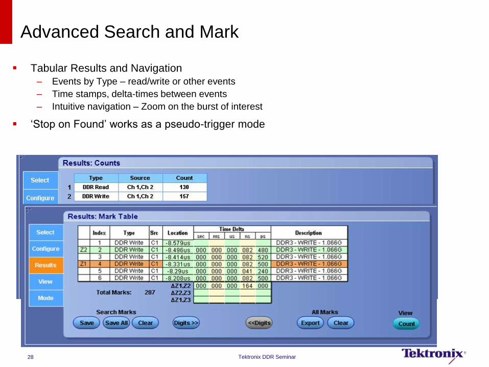
Advanced Search and Mark
Tabular Results and Navigation
– Events by Type – read/write or other events
– Time stamps, delta-times between events
– Intuitive navigation – Zoom on the burst of interest
‘Stop on Found’ works as a pseudo-trigger mode
28 Tektronix DDR Seminar
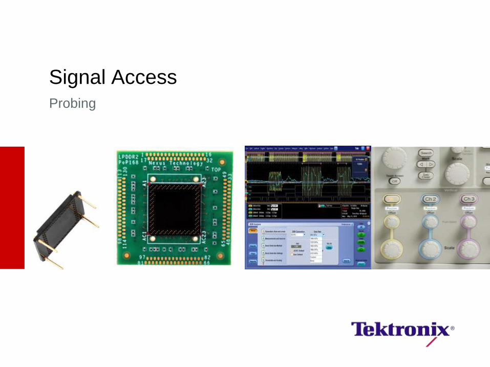
Signal Access Probing
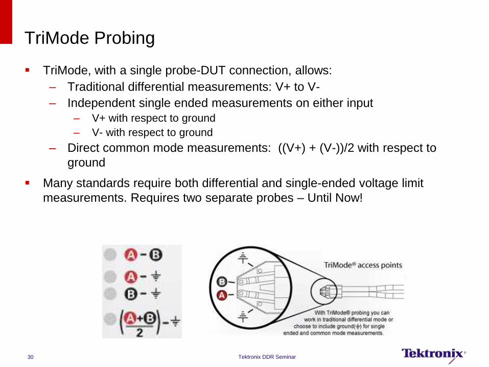
TriMode Probing
TriMode, with a single probe-DUT connection, allows:
– Traditional differential measurements: V+ to V-
– Independent single ended measurements on either input
– V+ with respect to ground
– V- with respect to ground
– Direct common mode measurements: ((V+) + (V-))/2 with respect to
ground
Many standards require both differential and single-ended voltage limit
measurements. Requires two separate probes – Until Now!
30 Tektronix DDR Seminar
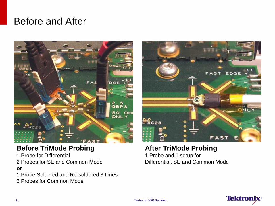
Before and After
Before TriMode Probing 1 Probe for Differential
2 Probes for SE and Common Mode
or
1 Probe Soldered and Re-soldered 3 times
2 Probes for Common Mode
After TriMode Probing 1 Probe and 1 setup for
Differential, SE and Common Mode
31 Tektronix DDR Seminar
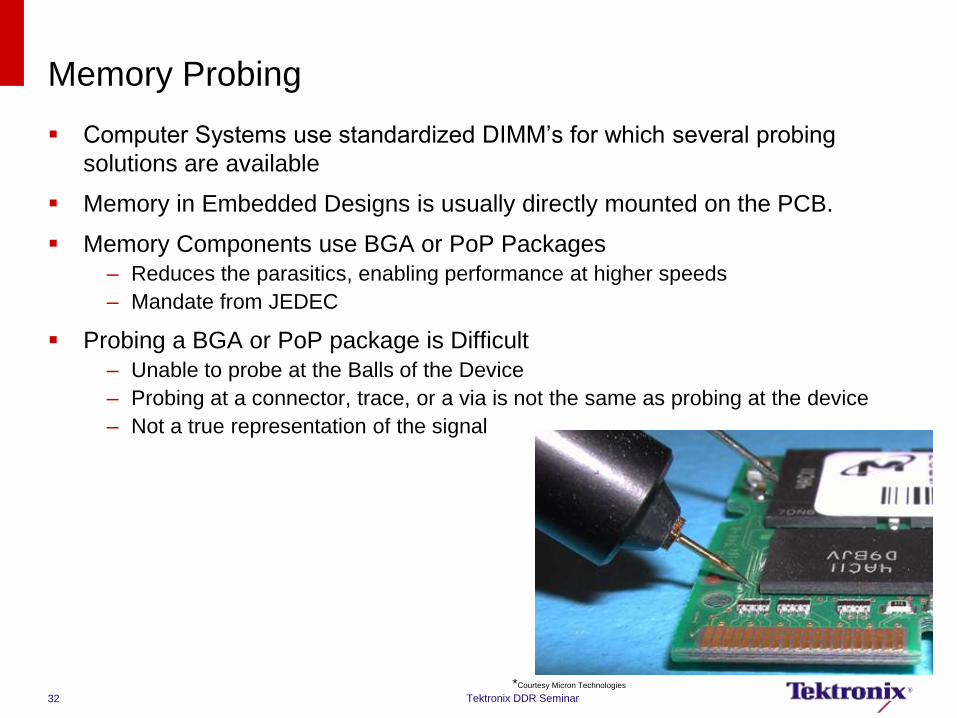
Memory Probing
Computer Systems use standardized DIMM’s for which several probing
solutions are available
Memory in Embedded Designs is usually directly mounted on the PCB.
Memory Components use BGA or PoP Packages
– Reduces the parasitics, enabling performance at higher speeds
– Mandate from JEDEC
Probing a BGA or PoP package is Difficult
– Unable to probe at the Balls of the Device
– Probing at a connector, trace, or a via is not the same as probing at the device
– Not a true representation of the signal
*Courtesy Micron Technologies
32 Tektronix DDR Seminar
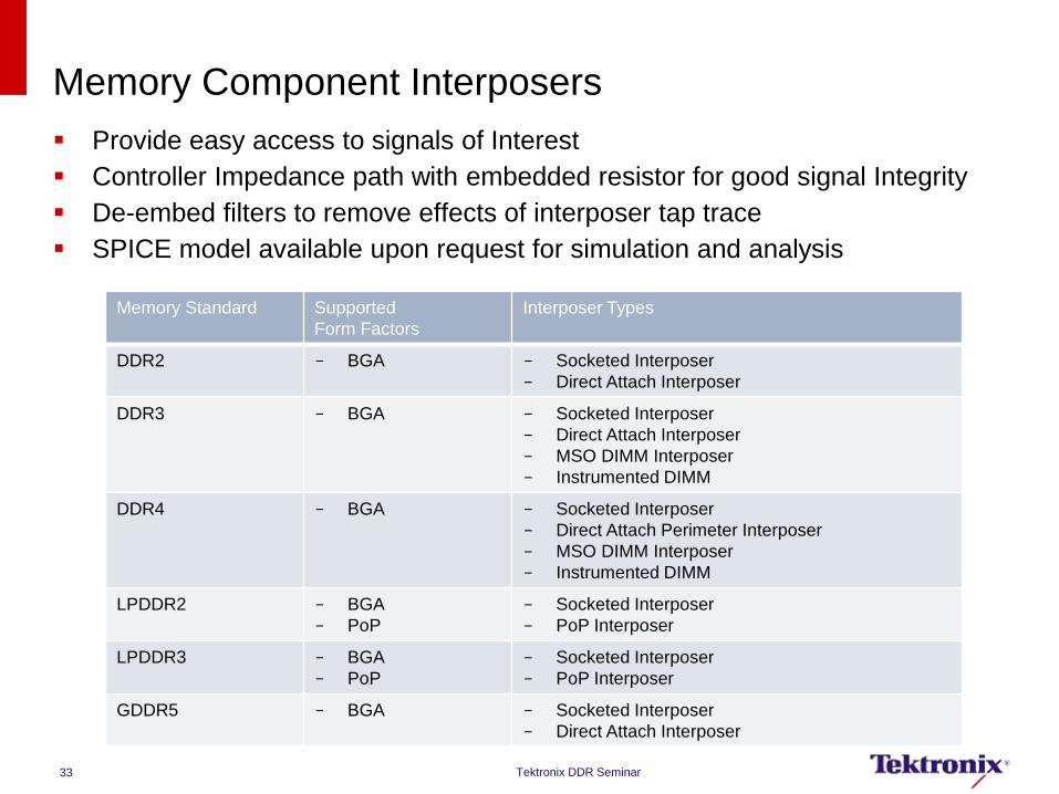
Memory Component Interposers
Memory Standard Supported
Form Factors
Interposer Types
DDR2 - BGA - Socketed Interposer
- Direct Attach Interposer
DDR3 - BGA
- Socketed Interposer
- Direct Attach Interposer
- MSO DIMM Interposer
- Instrumented DIMM
DDR4 - BGA - Socketed Interposer
- Direct Attach Perimeter Interposer
- MSO DIMM Interposer
- Instrumented DIMM
LPDDR2 - BGA
- PoP
- Socketed Interposer
- PoP Interposer
LPDDR3 - BGA
- PoP
- Socketed Interposer
- PoP Interposer
GDDR5 - BGA
- Socketed Interposer
- Direct Attach Interposer
Provide easy access to signals of Interest
Controller Impedance path with embedded resistor for good signal Integrity
De-embed filters to remove effects of interposer tap trace
SPICE model available upon request for simulation and analysis
33 Tektronix DDR Seminar
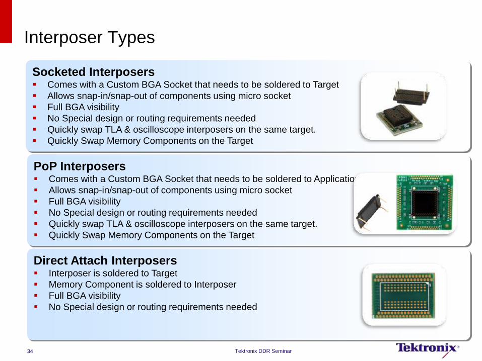
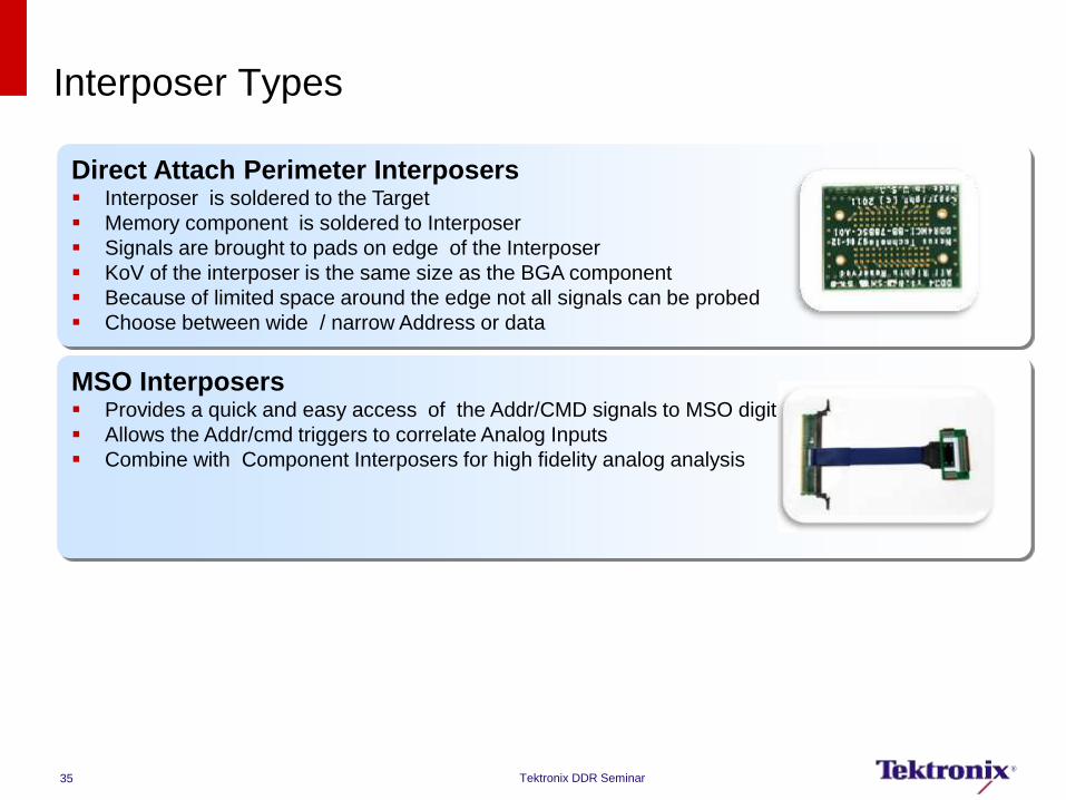
Interposer Types
Socketed Interposers Comes with a Custom BGA Socket that needs to be soldered to Target
Allows snap-in/snap-out of components using micro socket
Full BGA visibility
No Special design or routing requirements needed
Quickly swap TLA & oscilloscope interposers on the same target.
Quickly Swap Memory Components on the Target
PoP Interposers Comes with a Custom BGA Socket that needs to be soldered to Application Processor
Allows snap-in/snap-out of components using micro socket
Full BGA visibility
No Special design or routing requirements needed
Quickly swap TLA & oscilloscope interposers on the same target.
Quickly Swap Memory Components on the Target
Direct Attach Interposers Interposer is soldered to Target
Memory Component is soldered to Interposer
Full BGA visibility
No Special design or routing requirements needed
34 Tektronix DDR Seminar
Interposer Types
Direct Attach Perimeter Interposers Interposer is soldered to the Target
Memory component is soldered to Interposer
Signals are brought to pads on edge of the Interposer
KoV of the interposer is the same size as the BGA component
Because of limited space around the edge not all signals can be probed
Choose between wide / narrow Address or data
MSO Interposers Provides a quick and easy access of the Addr/CMD signals to MSO digital channel
Allows the Addr/cmd triggers to correlate Analog Inputs
Combine with Component Interposers for high fidelity analog analysis
35 Tektronix DDR Seminar
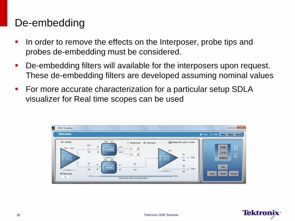
De-embedding
In order to remove the effects on the Interposer, probe tips and
probes de-embedding must be considered.
De-embedding filters will available for the interposers upon request.
These de-embedding filters are developed assuming nominal values
For more accurate characterization for a particular setup SDLA
visualizer for Real time scopes can be used
36 Tektronix DDR Seminar
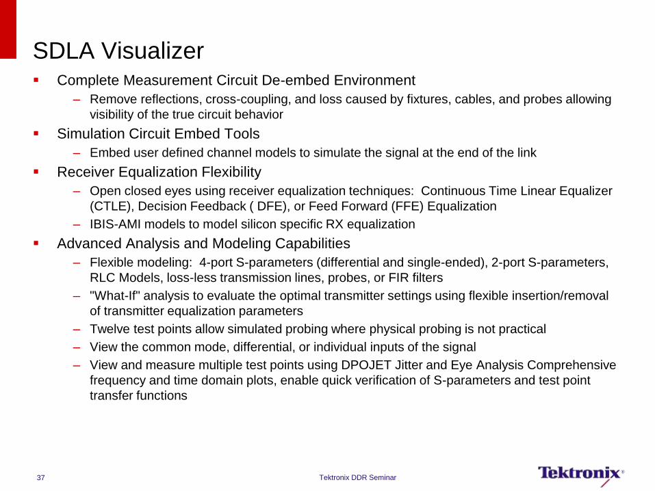
SDLA Visualizer Complete Measurement Circuit De-embed Environment
– Remove reflections, cross-coupling, and loss caused by fixtures, cables, and probes allowing
visibility of the true circuit behavior
Simulation Circuit Embed Tools
– Embed user defined channel models to simulate the signal at the end of the link
Receiver Equalization Flexibility
– Open closed eyes using receiver equalization techniques: Continuous Time Linear Equalizer
(CTLE), Decision Feedback ( DFE), or Feed Forward (FFE) Equalization
– IBIS-AMI models to model silicon specific RX equalization
Advanced Analysis and Modeling Capabilities
– Flexible modeling: 4-port S-parameters (differential and single-ended), 2-port S-parameters,
RLC Models, loss-less transmission lines, probes, or FIR filters
– "What-If" analysis to evaluate the optimal transmitter settings using flexible insertion/removal
of transmitter equalization parameters
– Twelve test points allow simulated probing where physical probing is not practical
– View the common mode, differential, or individual inputs of the signal
– View and measure multiple test points using DPOJET Jitter and Eye Analysis Comprehensive
frequency and time domain plots, enable quick verification of S-parameters and test point
transfer functions
37 Tektronix DDR Seminar
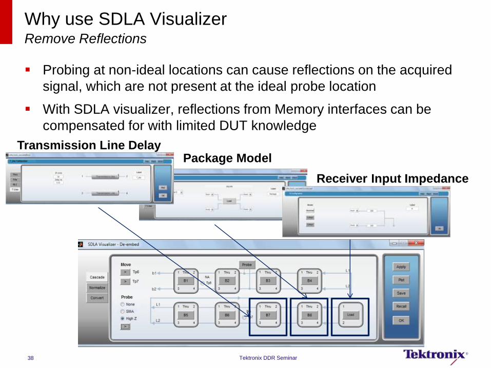
Why use SDLA Visualizer Remove Reflections
Probing at non-ideal locations can cause reflections on the acquired
signal, which are not present at the ideal probe location
With SDLA visualizer, reflections from Memory interfaces can be
compensated for with limited DUT knowledge
Tektronix DDR Seminar 38
Receiver Input Impedance
Package Model Transmission Line Delay

Remove Reflections Estimate Load Resistance and Transmission Line Delay
Use cursors to get ratio of reflected to
incident voltage.
Compute resistance as :
R = Z0 ( 1 + G ) / (1 - G)
Tune R to get best results. 220 ohms
was used
Tektronix DDR Seminar 39
G = (V2 – V1 ) / V1
G = (1.25 – 0.75 ) / 0.75
R = 200
Use cursor measurement to get delay
for round trip reflection.
Then divide by 2.
Td = 660ps / 2
Td = 330ps
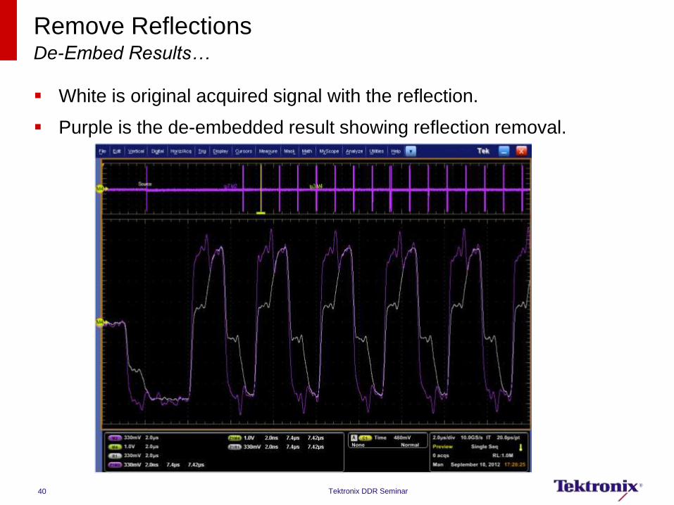
Remove Reflections De-Embed Results…
White is original acquired signal with the reflection.
Purple is the de-embedded result showing reflection removal.
Tektronix DDR Seminar 40
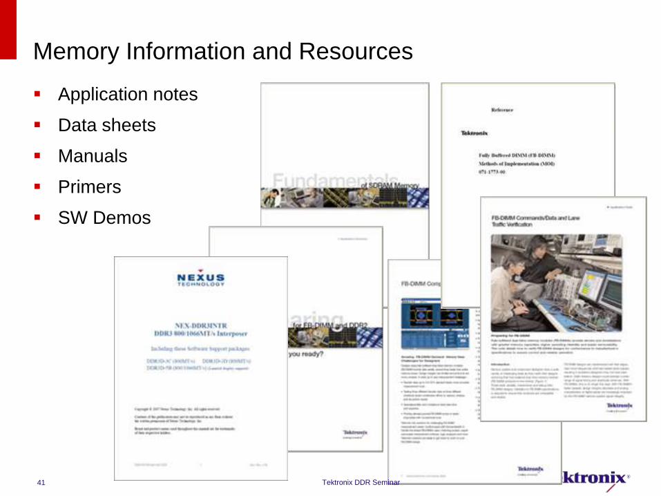
Memory Information and Resources
Application notes
Data sheets
Manuals
Primers
SW Demos
41 Tektronix DDR Seminar
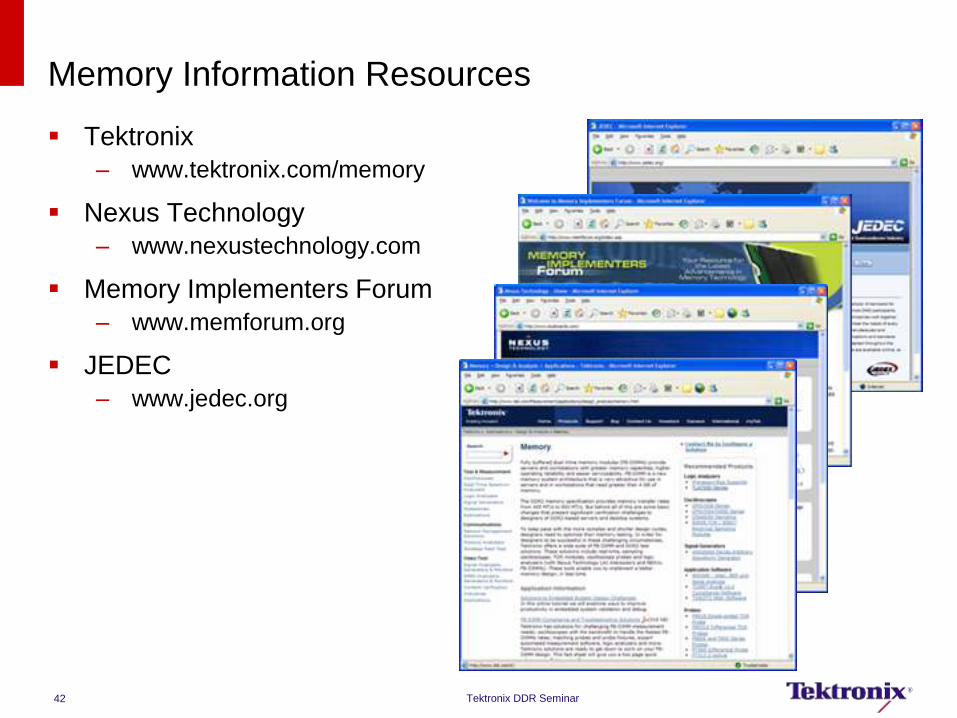
Memory Information Resources
Tektronix
– www.tektronix.com/memory
Nexus Technology
– www.nexustechnology.com
Memory Implementers Forum
– www.memforum.org
JEDEC
– www.jedec.org
42 Tektronix DDR Seminar
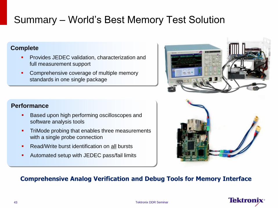
Performance
Based upon high performing oscilloscopes and
software analysis tools
TriMode probing that enables three measurements
with a single probe connection
Read/Write burst identification on all bursts
Automated setup with JEDEC pass/fail limits
Complete
Provides JEDEC validation, characterization and
full measurement support
Comprehensive coverage of multiple memory
standards in one single package
Summary – World’s Best Memory Test Solution
Comprehensive Analog Verification and Debug Tools for Memory Interface
43 Tektronix DDR Seminar
Thank You