Embed Size (px)
Citation preview
Dr. Tao Li 1
EEL 4744C: Microprocessor Applications
Lecture 10
Part 1
Analog Input & Output

Dr. Tao Li 2
• M&M: Chapter 11
Read Assignment

Dr. Tao Li 3
• To process continuous signals as functions oftime
• Advantages– free from noise (e.g. error resilient)– can be stored, retrieved, and manipulated by
computer (e.g. speech recognition)
• Disadvantages– loss of information– higher bandwidth requirement for transmission
Digitizing Signals

Dr. Tao Li 4
Data Acquisition System

Dr. Tao Li 5
• Transducers convert analog input to electrical signals(e.g. voltages or currents)
Transducer

Dr. Tao Li 6
• Signal conditioning: electrical isolation and buffering(e.g. protect from static discharges), amplification (e.g.produce necessary voltage for ADC), and bandwidthlimiting (e.g. low-pass filter to limit range of frequenciesfor digitization)
Signal Conditioning
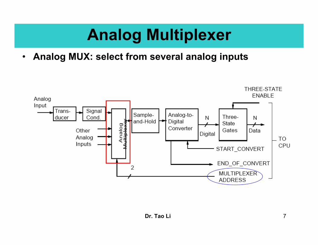
Dr. Tao Li 7
• Analog MUX: select from several analog inputs
Analog Multiplexer

Dr. Tao Li 8
• Sample-and-hold circuit holds signal steady while ADCconverts it– High-quality capacitor and high-speed semiconductor switch– Close switch for very short period, let capacitor charge, then
switch opened and voltage held for ADC during its conversiontime
– May be included within ADC device
Sample-and-Hold

Dr. Tao Li 9
• ADC converts sampled signal to digital values;has a word-size just like other digital devices
A/D Converter

Dr. Tao Li 10
• Shannon’s Theorem: sampling frequency must be atleast twice the signal frequency
• If not followed, then undersampled, which leads toaliasing and invalid signal reconstruction
• Signal conditioning circuit may include antialiasingfilter, helps here by attenuating frequencies above ½the sample freq.
• Nyquist frequency: the maximum frequency one cansample without aliasing (Nyquist frequency = fsample/2)
Sampling Theorem & Aliasing

Dr. Tao Li 11
• Normally interfaced to rest of system via parallel I/Ointerface circuit or parallel input port
• START_CONVERT control signal asserted by CPU tobegin the conversion
• END_CONVERT informs CPU when conversioncomplete (use via polling or interrupt)
A/D Conversion
Dr. Tao Li 12
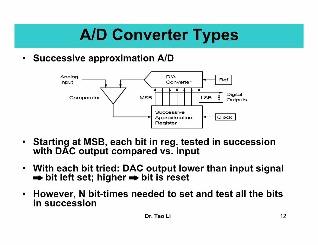
• Successive approximation A/D
• Starting at MSB, each bit in reg. tested in successionwith DAC output compared vs. input
• With each bit tried: DAC output lower than input signal⇒ bit left set; higher ⇒ bit is reset
• However, N bit-times needed to set and test all the bitsin succession
A/D Converter Types

Dr. Tao Li 13
• Has an up-down counter controlled by comparator
• If input signal higher or lower than DAC output, countercounts up or down, respectively
• Converter may quickly converge to correct digital valuewhen signal not changing quickly
Tracking A/D Converter

Dr. Tao Li 14
• Converter integrates input signal for period T1;afterwards, switch changed to minus ref. voltage andintegrator discharges to zero at constant rate; time todischarge is period T2 and gives a digital value
Integrating A/D Converter (Dual slope ADC)

Dr. Tao Li 15
• An array of 2N-1 parallel comparators that quicklyproduces output code in prop. time of comparators plusencoder/decoder logic; fast but costly
Parallel A/D Converter

Dr. Tao Li 16
• Has nearly the speed of flash ADC but lesscostly
Two Stage Parallel A/D Converter
Dr. Tao Li 17
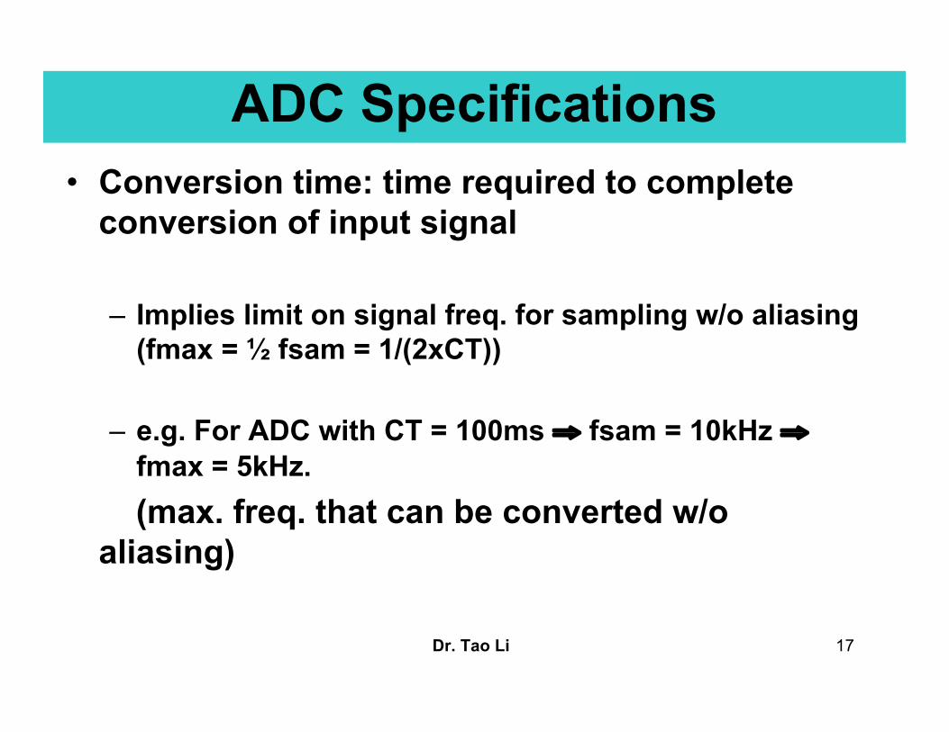
• Conversion time: time required to completeconversion of input signal
– Implies limit on signal freq. for sampling w/o aliasing(fmax = ½ fsam = 1/(2xCT))
– e.g. For ADC with CT = 100ms ⇒ fsam = 10kHz ⇒fmax = 5kHz.
(max. freq. that can be converted w/oaliasing)
ADC Specifications
Dr. Tao Li 18
• Resolution: several forms of term in use, suchas # of bits in ADC, smallest input signal forwhich ADC will produce a digital code
– full-scale signal ÷ 2N
– e.g. 8-bit ADC on 5V full-scale signal ⇒ res. is 5V/256= 19.5mV (0.4% of full scale value)
ADC Specifications

Dr. Tao Li 19
• Accuracy: ratio of smallest signal to measuredsignal; in %, describes how close measurementis to actual value– e.g. 8-bit ADC on 5V full-scale signal, accuracy w/
50mV signal is 19.5/50 = 39%
• Linearity: deviation in output codes vs. linefrom zero to full-scale; best is ± ½ of LSB
ADC Specifications

Dr. Tao Li 20
• Aperture time: time ADC is “looking” at inputsignal
– During this period, change in input signal may causeerror in output code
ADC Specifications
Dr. Tao Li 21
• Quantization error is fundamental in A/D conversiondue to resolution of ADC– Can be no less than ± ½ LSB
• Other sources of errors include:– Noise (desire peak-to-peak noise to be < ± ½ LSB; choose
appropriate ADC resolution or reduce the signal noise)
– Aliasing (include low-pass filter to attenuate freqs. aboveNyquist freq)
– Aperture time (if signal varies during this period, sample & holdcircuit achieve short aperture time))
ADC Errors
Dr. Tao Li 22
• Choose # of bits or resolution, speed orconversion time, type of digital code produced,etc
• Two ways to choose ADC resolution:– Find dynamic range of input signal to choose # of
bits• DR = Vmax / Vnoise , where Vmax is max. input signal,
Vnoise is peak-to-peak noise• For noise within ± ½ LSB, N ≥ log2 DR
– Choose based on resolution required in signal• N ≥ log2 Vmax / Vmin , where Vmin is required resolution
ADC Selection

Dr. Tao Li 23
• Choose ADC conversion time based on highest-frequency component sampled 2x or more
• Output code options for unipolar ADC (positivesignals) include unsigned binary and 1’scomplement; see Table 11-1
• Output code options for bipolar ADC (pos. &neg. signals) include 2’s complement, signed-magnitude, and offset binary; see Table 11-2
ADC Selection

Dr. Tao Li 24
• Example: consider ADC for ±5V peak-to-peakrange, 5mV peak-to-peak noise, and fmax =3kHz:– DR = 10V / 5mV = 2000– N ≥ log2 2000 ≥ 10.9 ⇒ N = 11 or more– Maximum conversion time is 1 / (2×3kHz) ≈ 167ms
ADC Selection

Dr. Tao Li 25
• DAC diagram
• Latch may be part of DAC or must beseparately interfaced
• Signal cond. block may be used to filter andsmooth the quantized output, and perhaps alsoisolation, voltage amplification, etc.
• Example of quantized DAC outputwaveform
D/A Conversion

Dr. Tao Li 26
• Basic DAC circuit is binary-weighted registerDAC– weighted current supplied to summing junction of
amplifier
D/A Converter Types

Dr. Tao Li 27
• R-2R ladder DAC circuit using single-pole,double-throw switches between ground andreference– binary-weighted current supplied to summing
junction
D/A Converter Types

Dr. Tao Li 28
• Resolution and linearity (same as before butw.r.t. output voltage)
• Settling time: time for output voltage to settlewithin specified error band (e.g. ± ½ LSB)
DAC Specifications

Dr. Tao Li 29
• Glitches: high-speed DACs may have problemswith glitches and settling time
• Glitch caused by asymmetrical switching in D/Aswitches (e.g. 1→0 switch faster than 0→1switch ⇒ glitch)
DAC Specifications
Dr. Tao Li 30
• Consider change in output on 8-bit DAC, from%10000000 to %01111111; would expect change from ½full-scale to one resolution less, but asymm. switchingcauses transitory sequence 10000000→00000000→01111111 ⇒ glitch on output signal!)
• Can be eliminated w/ sample-and-hold on DAC output,strobed to sample data after glitch and settling time
DAC Specifications

Dr. Tao Li 31
EEL 4744C: Microprocessor Applications
Lecture 10
Part 2
M68HC12 Analog Input
Dr. Tao Li 32
• SHE (old version): Chapter 12
• SHE (new version): Chapter 17
• Freescale HC12 Data Sheet: Chapter 17
Read Assignment

Dr. Tao Li 33
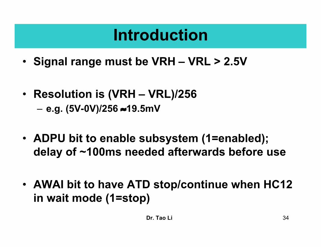
• 8-channel, multiplexed, 8-bit, successive approx. ADCwith sample-and-hold
• Linear to ±1 LSB accuracy in full temperature range w/no missing codes
• Both conversion time and S&H aperture time areprogrammable
• Uses VRH and VRL to optimize resolution over inputsignal range
• VRH usually set to input signal max. (but must be ≤ 6V);VRL to min. (but must be ≥ 0V)
Introduction
Dr. Tao Li 34
• Signal range must be VRH – VRL > 2.5V
• Resolution is (VRH – VRL)/256– e.g. (5V-0V)/256 ≈19.5mV
• ADPU bit to enable subsystem (1=enabled);delay of ~100ms needed afterwards before use
• AWAI bit to have ATD stop/continue when HC12in wait mode (1=stop)
Introduction

Dr. Tao Li 35
HC12 ADC Block Diagram
Analog Input Pins
Select which channels to convert
Built-in, Programmable Sample-and-Hold
Circuitry4/8 successive
conversions
A/D Power-upA/D Interrupt Flag and Enable

Dr. Tao Li 36
• A/D derives clock from P-clock; prescalar bitsPRS4-PRS0 for ÷2 (fastest) to ÷16 (slowest)– See Table 12-1
• Limits: max. and min. conversion freqs.permitted are 2MHz and 500kHz, respectively
• Final sample time stage selectable from 2-16clock periods (2,4,8,16) via SMP1:SMP0 bits– See Table 12-2
Introduction

Dr. Tao Li 37
Sampling & Conversion TimingATDCTL4 register controls the A/D Timing
Total conversion timeMin = 2 + 4 + 2 + 10 = 18
Max = 2 + 4 + 16 + 10 = 32
Prescaler select bits
Sample time select bits
(The maximum analog inputfrequencies)Nyquist Frequency =1/(2*total_conversion_time)= 1/(2*cycles*(1/ fad_clock)= 0.5* fad_clock/cycles
If fad_clock= 2MHz,The NyquistFrequency: 31.25~55.5 KHz
Dr. Tao Li 38
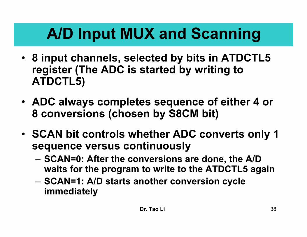
• 8 input channels, selected by bits in ATDCTL5register (The ADC is started by writing toATDCTL5)
• ADC always completes sequence of either 4 or8 conversions (chosen by S8CM bit)
• SCAN bit controls whether ADC converts only 1sequence versus continuously– SCAN=0: After the conversions are done, the A/D
waits for the program to write to the ATDCTL5 again– SCAN=1: A/D starts another conversion cycle
immediately
A/D Input MUX and Scanning

Dr. Tao Li 39
• MULT bit determines if 4/8 sequences done onsingle or successive channels
• Channel select bits CD-CA choose whichchannel (s) converted– Unused ones can be used for GP input via Port AD as
before
• See Table 12-3 for details
• The ADC has 8, 16-bit result registers (only thehigh-order 8 bits are used for HC12)
A/D Input MUX and Scanning

Dr. Tao Li 40
• ADC can generate interrupts when conversionsequence complete, or user may poll flag
• SCF (sequence complete flag) bit set when the 4/8conversion sequence is done
• Also, 8 conversion complete flags (CCF7-CCF0)associated with the A/D result registers– Set when current conversion writes into associated result
register
• These flags contained in 16-bit ATDSTAT status register
A/D Input Synchronization

Dr. Tao Li 41
• AFFC (A/D fast flag clear) bit controls howstatus flags are reset
– AFFC=0: 2-step process: (1) read status register; (2)if CCFn flag then read associated result register, or ifSCF then write to ATDCTL5 to start new conversion
– AFFC=1: fast mode: CCFn flag clears by readingassociated result register; SCF clears when firstresult register read
– Former typically used for polling, latter for interrupts
A/D Input Synchronization
Dr. Tao Li 42
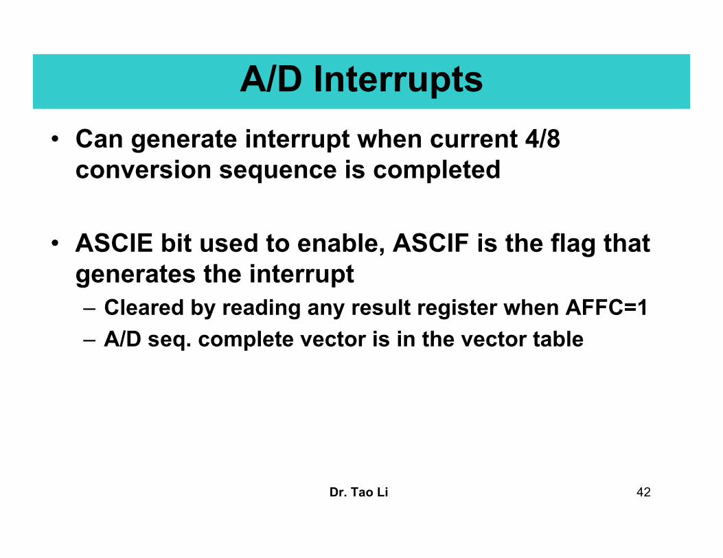
• Can generate interrupt when current 4/8conversion sequence is completed
• ASCIE bit used to enable, ASCIF is the flag thatgenerates the interrupt– Cleared by reading any result register when AFFC=1– A/D seq. complete vector is in the vector table
A/D Interrupts
Dr. Tao Li 43
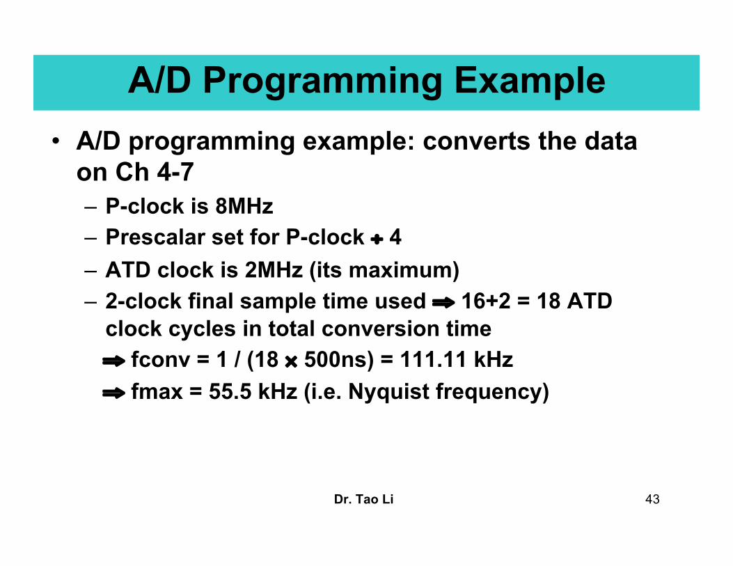
• A/D programming example: converts the dataon Ch 4-7– P-clock is 8MHz– Prescalar set for P-clock ÷ 4– ATD clock is 2MHz (its maximum)– 2-clock final sample time used ⇒ 16+2 = 18 ATD
clock cycles in total conversion time ⇒ fconv = 1 / (18 × 500ns) = 111.11 kHz ⇒ fmax = 55.5 kHz (i.e. Nyquist frequency)
A/D Programming Example

Dr. Tao Li 44
A/D Programming Example; A/D control registersATDCTL2: EQU $62ATDCTL4: EQU $64ATDCTL5: EQU $65ADR0H: EQU $70 ; Results registersADR1H: EQU $72ADR2H: EQU $74ADR3H: EQU $76ATDSTAT: EQU $66 ; A/D status registerSCF: EQU %10000000 ; Seq complete flagAFFC: EQU %01000000 ; Fast clearAWAI: EQU %00100000 ; A/D wait modeASCIE: EQU %00000010 ; SCF interrupt enableADPU: EQU %10000000 ; A/D power up bitSMP: EQU %01100000 ; SMP0 and SMP1 bitsPRS0: EQU %00000001 ; PRS0 bit; AD Mode: S8CM=0 4 conversion sequence; SCAN=0 Single conversion; MULT=1 4 conversions on channels 4-7; CD,CC,CB, CA=01xx Analog channel 4-7ADMODE: EQU %00010100

Dr. Tao Li 45
A/D Programming Example; Power up the A/D
bset ATDCTL2,ADPU; Generate a "short" delay > 100 microsec
ldaa #!200 ; 200 loops fordelay: nop ; 800 clock cycles
dbne a,delay; Now set up the A/D; Normal flag clearing, run in WAIT mode, no interrupts
bclr ATDCTL2,AFFC|AWAI|ASCIE; Select 2 clock sample time and divide by 4 prescaler:; Assume P clock is 8 MHz
bclr ATDCTL4,SMP ; Select 2 sample timebset ATDCTL4,PRS0 ; 2 MHz conversion freq
; Start the conversion by writing the scan select information to ATDCTL5loop: ldaa #ADMODE
staa ATDCTL5; And wait until conversion donespin: brclr ATDSTAT,SCF,spin; Get the channel 4 value
clra ; set A=0ldab ADR0H ; Channel 4 is here


![Perception Deception: Physical Adversarial Attack Challenges and … · 2019. 12. 21. · Dr. Tao Wei Dr. Yunhan Jia Dr. Zhenyu(Edward) Zhong edwardzhong [at] baidu DOT com Weilin](https://img.pdfslide.us/doc/110x75/60b65e55da6df575da620eae/perception-deception-physical-adversarial-attack-challenges-and-2019-12-21.jpg)