Embed Size (px)
Citation preview
ANALOG ELECTRONIC LAB (EE-222-F)
DEPARTMENT OF ELECTRICAL AND ELECTRONICS ENGINEERING DRONACHARY COLLEGE OF ENGINEERINGPage 1
ANALOG ELECTRONICS LAB
(EE-222-F)
IV SEMESTER
Electrical and Electronics Engineering
DEPARTMENT OF ELECTRICAL & ELECTRONICS DRONACHARAY COLLEGE OF ENGINEERING
KHENTAWAS, GURGAON-123506
ANALOG ELECTRONIC LAB (EE-222-F)
DEPARTMENT OF ELECTRICAL AND ELECTRONICS ENGINEERING DRONACHARY COLLEGE OF ENGINEERINGPage 2
ANALOG ELECTRONICS LAB LIST OF EXPERIMENTS
S.NO. Name of Experiment Page No.
1. To get familiar with working knowledge of the following Instruments. (a) CRO (b) Multimeter (c) Function generator (d) Regulated power supply (e) Active passive components (f) Bread Board
3-11
2. Study of V-I Characteristics of a Diode. 12-14
3(a). 3(b). 3(c).
To study and draw the characteristics of half wave and full wave rectifiers. To study and draw the characteristics of rectifier filter circuit. Study of Clipping & Clamping circuit.
15-17 18-21 22-25
4. To study zener diode characteristics.
26-29
5. To study zener diode as voltage regulator.
30-31
6(a).
6(b).
6(c).
To Study the characteristics of transistor in Common Base configuration. To plot and study the input and output characteristics of BJT in common-emitter configuration. Graphical determination of small signal hybrid parameter of BJT. Graphical determination of small signal hybrid parameter of bipolar junction transistor
32-34
35-36 37-39
7. To study and draw the characteristics of FET in common source configuration
40-42
8. Study characteristics of SCR.
43-44
9. Study of characteristics of DIAC. 45-46
10. To plot V-I characteristic of TRIAC.
47-49
11. To study and draw the characteristics of FET in common drain configuration.
50-52
12. To Study the Series and Shunt Voltage Regulator.
53
13. Study of frequency response of active filters HP, LP & BP.
54-59
ANALOG ELECTRONIC LAB (EE-222-F)
DEPARTMENT OF ELECTRICAL AND ELECTRONICS ENGINEERING DRONACHARY COLLEGE OF ENGINEERINGPage 3
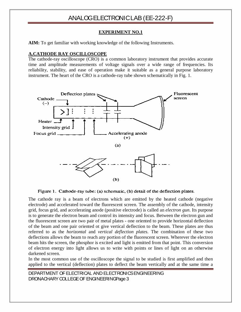
EXPERIMENT NO.1 AIM: To get familiar with working knowledge of the following Instruments. A.CATHODE RAY OSCILLOSCOPE The cathode-ray oscilloscope (CRO) is a common laboratory instrument that provides accurate time and amplitude measurements of voltage signals over a wide range of frequencies. Its reliability, stability, and ease of operation make it suitable as a general purpose laboratory instrument. The heart of the CRO is a cathode-ray tube shown schematically in Fig. 1.
The cathode ray is a beam of electrons which are emitted by the heated cathode (negative electrode) and accelerated toward the fluorescent screen. The assembly of the cathode, intensity grid, focus grid, and accelerating anode (positive electrode) is called an electron gun. Its purpose is to generate the electron beam and control its intensity and focus. Between the electron gun and the fluorescent screen are two pair of metal plates - one oriented to provide horizontal deflection of the beam and one pair oriented ot give vertical deflection to the beam. These plates are thus referred to as the horizontal and vertical deflection plates. The combination of these two deflections allows the beam to reach any portion of the fluorescent screen. Wherever the electron beam hits the screen, the phosphor is excited and light is emitted from that point. This conversion of electron energy into light allows us to write with points or lines of light on an otherwise darkened screen. In the most common use of the oscilloscope the signal to be studied is first amplified and then applied to the vertical (deflection) plates to deflect the beam vertically and at the same time a
ANALOG ELECTRONIC LAB (EE-222-F)
DEPARTMENT OF ELECTRICAL AND ELECTRONICS ENGINEERING DRONACHARY COLLEGE OF ENGINEERINGPage 4
voltage that increases linearly with time is applied to the horizontal (deflection) plates thus causing the beam to be deflected horizontally at a uniform (constant> rate. The signal applied to the vertical plates is thus displayed on the screen as a function of time. The horizontal axis serves as a uniform time scale. The linear deflection or sweep of the beam horizontally is accomplished by use of a sweep generator that is incorporated in the oscilloscope circuitry. The voltage output of such a generator is that of a saw tooth wave as shown in Fig. 2. Application of one cycle of this voltage difference, which increases linearly with time, to the horizontal plates causes the beam to be deflected linearly with time across the tube face. When the voltage suddenly falls to zero, as at points (a) (b) (c), etc...., the end of each sweep - the beam flies back to its initial position. The horizontal deflection of the beam is repeated periodically, the frequency of this periodicity is adjustable by external controls.
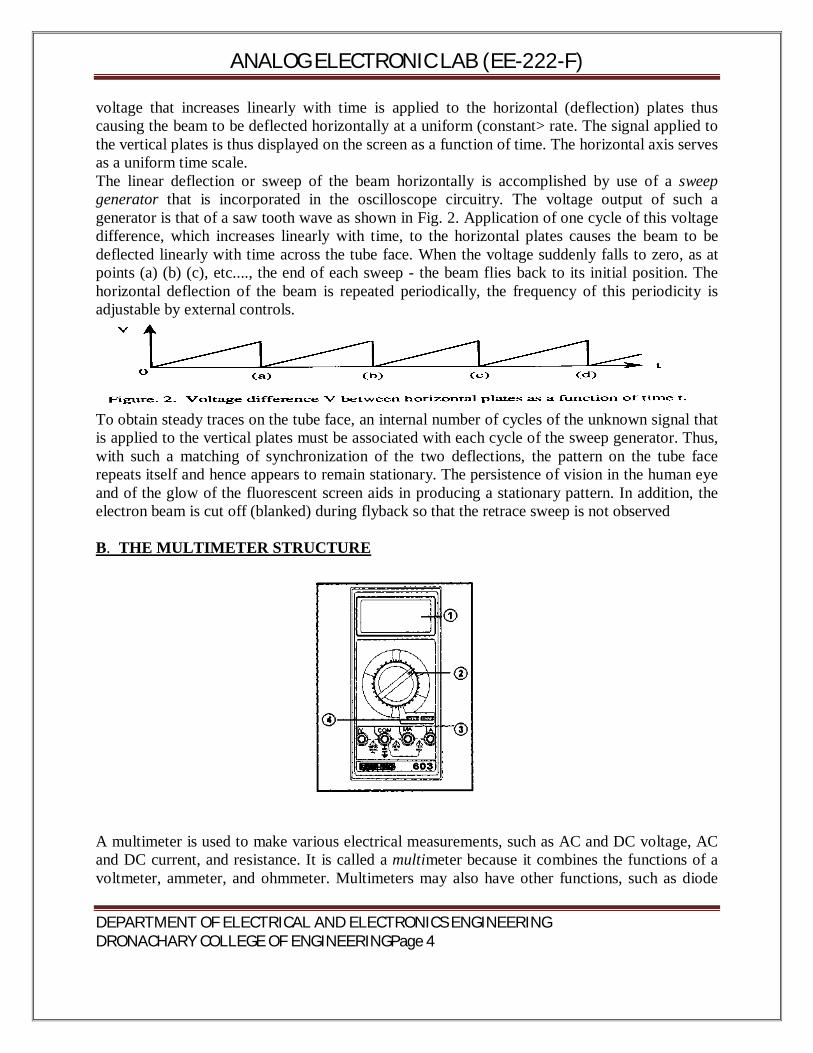
To obtain steady traces on the tube face, an internal number of cycles of the unknown signal that is applied to the vertical plates must be associated with each cycle of the sweep generator. Thus, with such a matching of synchronization of the two deflections, the pattern on the tube face repeats itself and hence appears to remain stationary. The persistence of vision in the human eye and of the glow of the fluorescent screen aids in producing a stationary pattern. In addition, the electron beam is cut off (blanked) during flyback so that the retrace sweep is not observed B. THE MULTIMETER STRUCTURE A multimeter is used to make various electrical measurements, such as AC and DC voltage, AC and DC current, and resistance. It is called a multimeter because it combines the functions of a voltmeter, ammeter, and ohmmeter. Multimeters may also have other functions, such as diode
ANALOG ELECTRONIC LAB (EE-222-F)
DEPARTMENT OF ELECTRICAL AND ELECTRONICS ENGINEERING DRONACHARY COLLEGE OF ENGINEERINGPage 5
and continuity tests. The descriptions and pictures that follow are specific to the Fluke 73 Series III Multimeter, but other multimeters are similar. Important note: The most common mistake when using a multimeter is not switching the test leads when switching between current sensing and any other type of sensing (voltage, resistance). It is critical that the test leads be in the proper jacks for the measurement you are making. Safety Information
Be sure the test leads and rotary switch are in the correct position for the desired measurement. Never use the meter if the meter or the test leads look damaged. Never measure resistance in a circuit when power is applied. Never touch the probes to a voltage source when a test lead is plugged into the 10 A or 300 mA
input jack. To avoid damage or injury, never use the meter on circuits that exceed 4800 watts. Never apply more than the rated voltage between any input jack and earth ground (600 V for the
Fluke 73). Be careful when working with voltages above 60 V DC or 30 V AC rms. Such voltages pose a
shock hazard. Keep your fingers behind the finger guards on the test probes when making measurements. To avoid false readings, which could lead to possible electric shock or personal injury, replace
the battery as soon as the battery indicator appears. C. FUNCTION GENERATOR A function generator is a device that can produce various patterns of voltage at a variety of frequencies and amplitudes. It is used to test the response of circuits to common input signals. The electrical leads from the device are attached to the ground and signal input terminals of the device under test.
ANALOG ELECTRONIC LAB (EE-222-F)
DEPARTMENT OF ELECTRICAL AND ELECTRONICS ENGINEERING DRONACHARY COLLEGE OF ENGINEERINGPage 6
Features and controls
Most function generators allow the user to choose the shape of the output from a small number of options.
-Square wave - The signal goes directly from high to low voltage. -Sine wave - The signal curves like a sinusoid from high to low voltage. -Triangle wave - The signal goes from high to low voltage at a fixed rate
The amplitude control on a function generator varies the voltage difference between the high and low voltage of the output signal.
The direct current (DC) offset control on a function generator varies the average voltage of a signal relative to the ground.
The frequency control of a function generator controls the rate at which output signal oscillates. On some function generators, the frequency control is a combination of different controls.
One set of controls chooses the broad frequency range (order of magnitude) and the other selects the precise frequency. This allows the function generator to handle the enormous variation in frequency scale needed for signals.
How to use a function generator? After powering on the function generator, the output signal needs to be configured to
the desired shape. Typically, this means connecting the signal and ground leads to an oscilloscope to check the controls.
Adjust the function generator until the output signal is correct, then attach the signal and ground leads from the function generator to the input and ground of the device under test.
ANALOG ELECTRONIC LAB (EE-222-F)
DEPARTMENT OF ELECTRICAL AND ELECTRONICS ENGINEERING DRONACHARY COLLEGE OF ENGINEERINGPage 7
For some applications, the negative lead of the function generator should attach to a negative input of the device, but usually attaching to ground is sufficient.
Conclusions A function generator is a device that can produce various patterns of voltage at a variety
of frequencies and amplitudes. D. REGULATED POWER SUPPLY Types of Power Supply There are many types of power supply. Most are designed to convert high voltage AC mains electricity to a suitable low voltage supply for electronics circuits and other devices. A power supply can by broken down into a series of blocks, each of which performs a particular function. For example a 5V regulated supply:
Each of the blocks is described in more detail below:
Transformer - steps down high voltage AC mains to low voltage AC. Rectifier - converts AC to DC, but the DC output is varying. Smoothing - smooths the DC from varying greatly to a small ripple. Regulator - eliminates ripple by setting DC output to a fixed voltage
1. POWER: Push button switch for supplying power to instrument. 2. OUTPUT ON: Push button for switching On / Off all the three output voltages. 3 & 6 V/mA (Push button): For switching the display from voltage to current reading or vice versa. When pushbuttons are pressed, the current supplied from the terminals 12 & 17 is displayed with a resolution of 1mA. In released position voltages across the terminals 12 & 17 are displayed with a resolution of 0.1 V. 4 & 7 DIGITAL DISPLAYS (7-Segment LED): Dual display with two 3-digit readout for output voltage and current. On the left side of the instrument the voltage and current readings for terminals 3 is indicated. The corresponding values for the terminals 4 are indicated on the right side of the display. 5 & 8 V & mA INDICATORS:
ANALOG ELECTRONIC LAB (EE-222-F)
DEPARTMENT OF ELECTRICAL AND ELECTRONICS ENGINEERING DRONACHARY COLLEGE OF ENGINEERINGPage 8
Two LEDs indicate the unit of the display. The mA LED flashes when the 0 – 30VDC output is used in constant current mode, or output current required is in excess of specified value, in CV mode. E.ACTIVE, PASSIVE COMPONENTS An electronic component is a basic electronic element and may be available in a discrete form (a discrete device or discrete component) having two or more electrical terminals (or leads). These are intended to be connected together, usually by soldering to a printed circuit board, in order to create an electronic circuit(a discrete circuit) with a particular function (for example an amplifier, radio receiver, or oscillator). Basic electronic components may be packaged discretely, as arrays or networks of like components, or integrated inside of packages such as semiconductor integrated circuits, hybrid integrated circuits, or thick film devices.
A component may be classified as passive or active. The strict physics definition treats passive components as ones that cannot supply energy themselves, whereas a battery would be seen as an active component since it truly acts as a source of energy.
Passive components are ones which cannot introduce net energy into the circuit they are connected to. They also cannot rely on a source of power except for what is available from the (AC) circuit they are connected to. As a consequence they are unable to amplify (increase the power of a signal), although they may well increase a voltage or current such as is done by a transformer or resonant circuit. Among passive components are familiar two-terminal components such as resistors, capacitors, inductors, and transformers.
Active components rely on a source of energy (usually from the DC circuit, which we have chosen to ignore) and are usually able to inject power into a circuit although this is not part of the definition[1]. This includes amplifying components such as transistors, triode vacuum tubes(valves), and tunnel diodes. Passive components can be further divided into lossless and lossy components:
ANALOG ELECTRONIC LAB (EE-222-F)
DEPARTMENT OF ELECTRICAL AND ELECTRONICS ENGINEERING DRONACHARY COLLEGE OF ENGINEERINGPage 9
Lossless components do not have a net power flow into or out of the component. This would include ideal capacitors, inductors, transformers, and the (theoretical) gyrator.
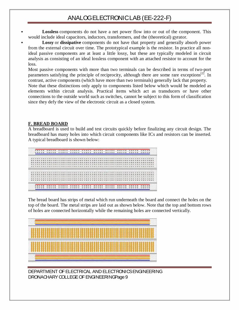
Lossy or dissipative components do not have that property and generally absorb power from the external circuit over time. The prototypical example is the resistor. In practice all non-ideal passive components are at least a little lossy, but these are typically modeled in circuit analysis as consisting of an ideal lossless component with an attached resistor to account for the loss. Most passive components with more than two terminals can be described in terms of two-port parameters satisfying the principle of reciprocity, although there are some rare exceptions[2]. In contrast, active components (which have more than two terminals) generally lack that property. Note that these distinctions only apply to components listed below which would be modeled as elements within circuit analysis. Practical items which act as transducers or have other connections to the outside world such as switches, cannot be subject to this form of classification since they defy the view of the electronic circuit as a closed system. F. BREAD BOARD A breadboard is used to build and test circuits quickly before finalizing any circuit design. The breadboard has many holes into which circuit components like ICs and resistors can be inserted. A typical breadboard is shown below:
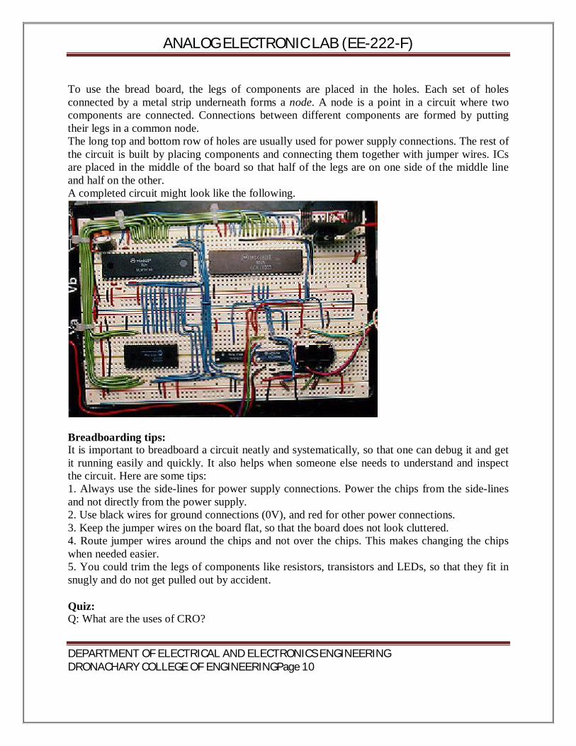
The bread board has strips of metal which run underneath the board and connect the holes on the top of the board. The metal strips are laid out as shown below. Note that the top and bottom rows of holes are connected horizontally while the remaining holes are connected vertically.
ANALOG ELECTRONIC LAB (EE-222-F)
DEPARTMENT OF ELECTRICAL AND ELECTRONICS ENGINEERING DRONACHARY COLLEGE OF ENGINEERINGPage 10
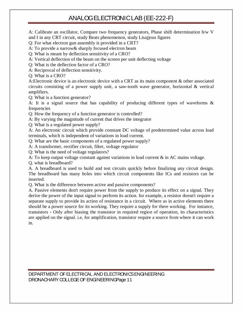
To use the bread board, the legs of components are placed in the holes. Each set of holes connected by a metal strip underneath forms a node. A node is a point in a circuit where two components are connected. Connections between different components are formed by putting their legs in a common node. The long top and bottom row of holes are usually used for power supply connections. The rest of the circuit is built by placing components and connecting them together with jumper wires. ICs are placed in the middle of the board so that half of the legs are on one side of the middle line and half on the other. A completed circuit might look like the following.
Breadboarding tips: It is important to breadboard a circuit neatly and systematically, so that one can debug it and get it running easily and quickly. It also helps when someone else needs to understand and inspect the circuit. Here are some tips: 1. Always use the side-lines for power supply connections. Power the chips from the side-lines and not directly from the power supply. 2. Use black wires for ground connections (0V), and red for other power connections. 3. Keep the jumper wires on the board flat, so that the board does not look cluttered. 4. Route jumper wires around the chips and not over the chips. This makes changing the chips when needed easier. 5. You could trim the legs of components like resistors, transistors and LEDs, so that they fit in snugly and do not get pulled out by accident. Quiz: Q: What are the uses of CRO?
ANALOG ELECTRONIC LAB (EE-222-F)
DEPARTMENT OF ELECTRICAL AND ELECTRONICS ENGINEERING DRONACHARY COLLEGE OF ENGINEERINGPage 11
A: Calibrate an oscillator, Compare two frequency generators, Phase shift determination b/w V and I in any CRT circuit, study Beats phenomenon, study Lisajjous figures Q: For what electron gun assembly is provided in a CRT? A: To provide a narrow& sharply focused electron beam Q: What is meant by deflection sensitivity of a CRO? A: Vertical deflection of the beam on the screen per unit deflecting voltage Q: What is the deflection factor of a CRO? A: Reciprocal of deflection sensitivity. Q: What is a CRO? A:Electronic device is an electronic device with a CRT as its main component & other associated circuits consisting of a power supply unit, a saw-tooth wave generator, horizontal & vertical amplifiers. Q: What is a function generator? A: It is a signal source that has capability of producing different types of waveforms & frequencies Q: How the frequency of a function generator is controlled? A: By varying the magnitude of current that drives the integrator Q: What is a regulated power supply? A: An electronic circuit which provide constant DC voltage of predetermined value across load terminals, which is independent of variations in load current. Q: What are the basic components of a regulated power supply? A: A transformer, rectifier circuit, filter, voltage regulator Q: What is the need of voltage regulators? A: To keep output voltage constant against variations in load current & in AC mains voltage. Q. what is breadboard? A. A breadboard is used to build and test circuits quickly before finalizing any circuit design. The breadboard has many holes into which circuit components like ICs and resistors can be inserted. Q. What is the difference between active and passive components? A. Passive elements don't require power from the supply to produce its effect on a signal. They derive the power of the input signal to perform its action. for example, a resistor doesn't require a separate supply to provide its action of resistance in a circuit. Where as in active elements there should be a power source for its working. They require a supply for there working. For instance, transistors - Only after biasing the transistor in required region of operation, its characteristics are applied on the signal. i.e, for amplification, transistor require a source from where it can work in.
ANALOG ELECTRONIC LAB (EE-222-F)
DEPARTMENT OF ELECTRICAL AND ELECTRONICS ENGINEERING DRONACHARY COLLEGE OF ENGINEERINGPage 12
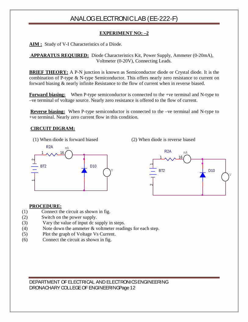
EXPERIMENT NO: –2 AIM : Study of V-I Characteristics of a Diode. APPARATUS REQUIRED: Diode Characteristics Kit, Power Supply, Ammeter (0-20mA), Voltmeter (0-20V), Connecting Leads. BRIEF THEORY: A P-N junction is known as Semiconductor diode or Crystal diode. It is the combination of P-type & N-type Semiconductor. This offers nearly zero resistance to current on forward biasing & nearly infinite Resistance to the flow of current when in reverse biased. Forward biasing: When P-type semiconductor is connected to the +ve terminal and N-type to –ve terminal of voltage source. Nearly zero resistance is offered to the flow of current. Reverse biasing: When P-type semiconductor is connected to the –ve terminal and N-type to +ve terminal. Nearly zero current flow in this condition. CIRCUIT DIGRAM: (1) When diode is forward biased (2) When diode is reverse biased
V
BT2
12
mAmA
V D10
R2A1 16
R2A1 16
BT2
12
D10
PROCEDURE:
(1) Connect the circuit as shown in fig. (2) Switch on the power supply. (3) Vary the value of input dc supply in steps. (4) Note down the ammeter & voltmeter readings for each step. (5) Plot the graph of Voltage Vs Current. (6) Connect the circuit as shown in fig.
ANALOG ELECTRONIC LAB (EE-222-F)
DEPARTMENT OF ELECTRICAL AND ELECTRONICS ENGINEERING DRONACHARY COLLEGE OF ENGINEERINGPage 13
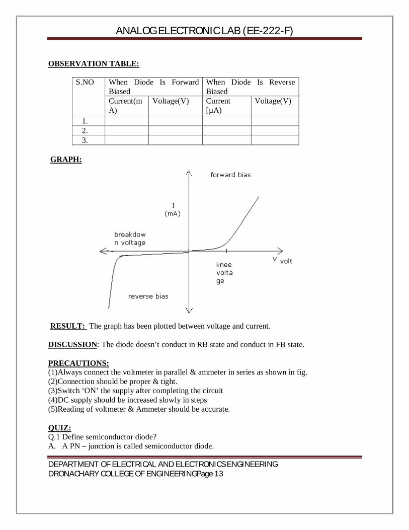
OBSERVATION TABLE:
S.NO When Diode Is Forward Biased
When Diode Is Reverse Biased
Current(mA)
Voltage(V) Current [µA)
Voltage(V)
1. 2. 3.
GRAPH:
RESULT: The graph has been plotted between voltage and current. DISCUSSION: The diode doesn’t conduct in RB state and conduct in FB state. PRECAUTIONS: (1)Always connect the voltmeter in parallel & ammeter in series as shown in fig. (2)Connection should be proper & tight. (3)Switch ‘ON’ the supply after completing the circuit (4)DC supply should be increased slowly in steps (5)Reading of voltmeter & Ammeter should be accurate. QUIZ: Q.1 Define semiconductor diode? A. A PN – junction is called semiconductor diode.
ANALOG ELECTRONIC LAB (EE-222-F)
DEPARTMENT OF ELECTRICAL AND ELECTRONICS ENGINEERING DRONACHARY COLLEGE OF ENGINEERINGPage 14
Q.2 Define depletion layer? A. The region having uncompensated acceptor and donor ions. Q.3 what do you mean by forward biased? A. When +ve terminal of battery is connected to P side & -ve terminal to N side of diode. Q.4 what do you mean by reverse biased? A. When +ve terminal of battery is connected to N side & -ve terminal to P side of diode. Q.5 Define Knee voltage? A. The forward voltage at which current through the junction starts increasing rapidly. Q.6 Define breakdown voltage? A. Reverse voltage at which PN junction breaks down with sudden rise in reverse current. Q.7 Define max. Forward current? A. It is highest instantaneous forward current that a PN junction can conduct without damage to Junction. Q.8 Define max. Power rating? A. Max. Power that can be dissipated at junction without damage to it.
ANALOG ELECTRONIC LAB (EE-222-F)
DEPARTMENT OF ELECTRICAL AND ELECTRONICS ENGINEERING DRONACHARY COLLEGE OF ENGINEERINGPage 15
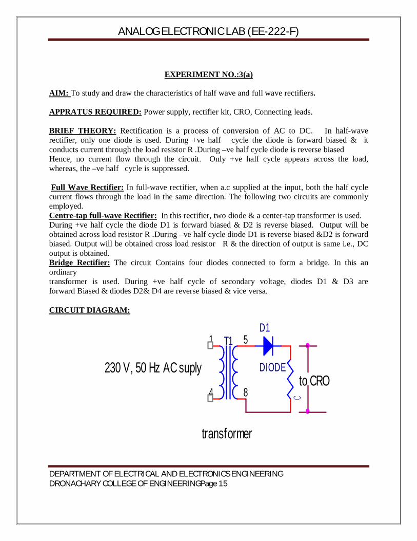
EXPERIMENT NO.:3(a) AIM: To study and draw the characteristics of half wave and full wave rectifiers. APPRATUS REQUIRED: Power supply, rectifier kit, CRO, Connecting leads. BRIEF THEORY: Rectification is a process of conversion of AC to DC. In half-wave rectifier, only one diode is used. During +ve half cycle the diode is forward biased & it conducts current through the load resistor R .During –ve half cycle diode is reverse biased Hence, no current flow through the circuit. Only +ve half cycle appears across the load, whereas, the –ve half cycle is suppressed. Full Wave Rectifier: In full-wave rectifier, when a.c supplied at the input, both the half cycle current flows through the load in the same direction. The following two circuits are commonly employed. Centre-tap full-wave Rectifier: In this rectifier, two diode & a center-tap transformer is used. During +ve half cycle the diode D1 is forward biased & D2 is reverse biased. Output will be obtained across load resistor R .During –ve half cycle diode D1 is reverse biased &D2 is forward biased. Output will be obtained cross load resistor R & the direction of output is same i.e., DC output is obtained. Bridge Rectifier: The circuit Contains four diodes connected to form a bridge. In this an ordinary transformer is used. During +ve half cycle of secondary voltage, diodes D1 & D3 are forward Biased & diodes D2& D4 are reverse biased & vice versa. CIRCUIT DIAGRAM:
transformer
to CRO
T11 5
4 8
D1
DIODE230 V, 50 Hz AC suply
C
ANALOG ELECTRONIC LAB (EE-222-F)
DEPARTMENT OF ELECTRICAL AND ELECTRONICS ENGINEERING DRONACHARY COLLEGE OF ENGINEERINGPage 16
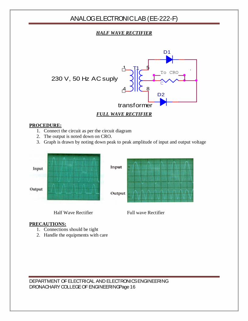
HALF WAVE RECTIFIER
To CRO
C230 V, 50 Hz AC suply
transformer
T11 5
4 8D2
D1
FULL WAVE RECTIFIER
PROCEDURE:
1. Connect the circuit as per the circuit diagram 2. The output is noted down on CRO. 3. Graph is drawn by noting down peak to peak amplitude of input and output voltage
Half Wave Rectifier Full wave Rectifier PRECAUTIONS:
1. Connections should be tight 2. Handle the equipments with care
ANALOG ELECTRONIC LAB (EE-222-F)
DEPARTMENT OF ELECTRICAL AND ELECTRONICS ENGINEERING DRONACHARY COLLEGE OF ENGINEERINGPage 17
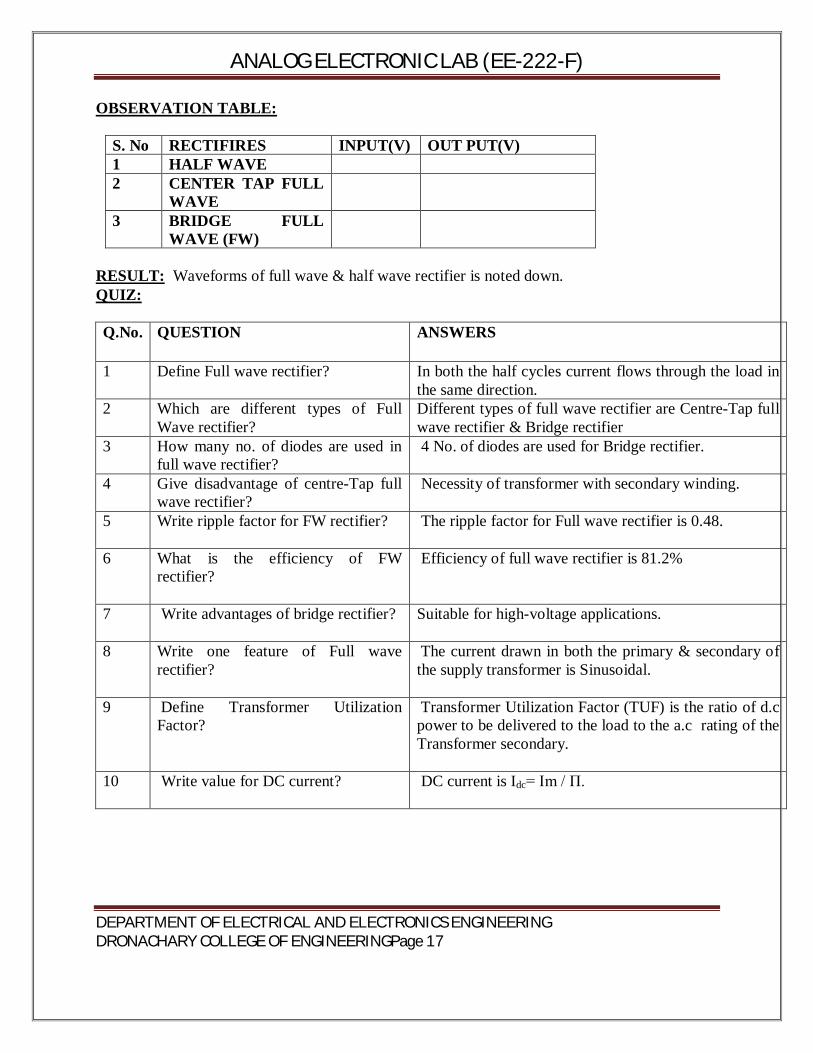
OBSERVATION TABLE:
S. No RECTIFIRES INPUT(V) OUT PUT(V) 1 HALF WAVE 2 CENTER TAP FULL
WAVE
3 BRIDGE FULL WAVE (FW)
RESULT: Waveforms of full wave & half wave rectifier is noted down. QUIZ: Q.No. QUESTION ANSWERS
1 Define Full wave rectifier? In both the half cycles current flows through the load in
the same direction. 2 Which are different types of Full
Wave rectifier? Different types of full wave rectifier are Centre-Tap full wave rectifier & Bridge rectifier
3 How many no. of diodes are used in full wave rectifier?
4 No. of diodes are used for Bridge rectifier.
4 Give disadvantage of centre-Tap full wave rectifier?
Necessity of transformer with secondary winding.
5 Write ripple factor for FW rectifier? The ripple factor for Full wave rectifier is 0.48.
6 What is the efficiency of FW rectifier?
Efficiency of full wave rectifier is 81.2%
7 Write advantages of bridge rectifier?
Suitable for high-voltage applications.
8 Write one feature of Full wave rectifier?
The current drawn in both the primary & secondary of the supply transformer is Sinusoidal.
9 Define Transformer Utilization Factor?
Transformer Utilization Factor (TUF) is the ratio of d.c power to be delivered to the load to the a.c rating of the Transformer secondary.
10 Write value for DC current?
DC current is Idc= Im / П.
ANALOG ELECTRONIC LAB (EE-222-F)
DEPARTMENT OF ELECTRICAL AND ELECTRONICS ENGINEERING DRONACHARY COLLEGE OF ENGINEERINGPage 18
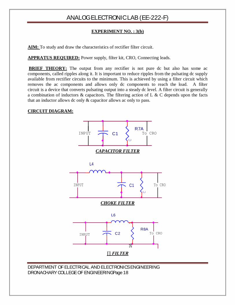
EXPERIMENT NO. : 3(b) AIM: To study and draw the characteristics of rectifier filter circuit. APPRATUS REQUIRED: Power supply, filter kit, CRO, Connecting leads. BRIEF THEORY: The output from any rectifier is not pure dc but also has some ac components, called ripples along it. It is important to reduce ripples from the pulsating dc supply available from rectifier circuits to the minimum. This is achieved by using a filter circuit which removes the ac components and allows only dc components to reach the load. A filter circuit is a device that converts pulsating output into a steady dc level. A filter circuit is generally a combination of inductors & capacitors. The filtering action of L & C depends upon the facts that an inductor allows dc only & capacitor allows ac only to pass. CIRCUIT DIAGRAM:
To CROINPUT C1C
R7A
CAPACITOR FILTER
INPUT C1
L4
C
To CRO
CHOKE FILTER
To CROR8A
116
C2INPUT
L6
∏ FILTER
ANALOG ELECTRONIC LAB (EE-222-F)
DEPARTMENT OF ELECTRICAL AND ELECTRONICS ENGINEERING DRONACHARY COLLEGE OF ENGINEERINGPage 19
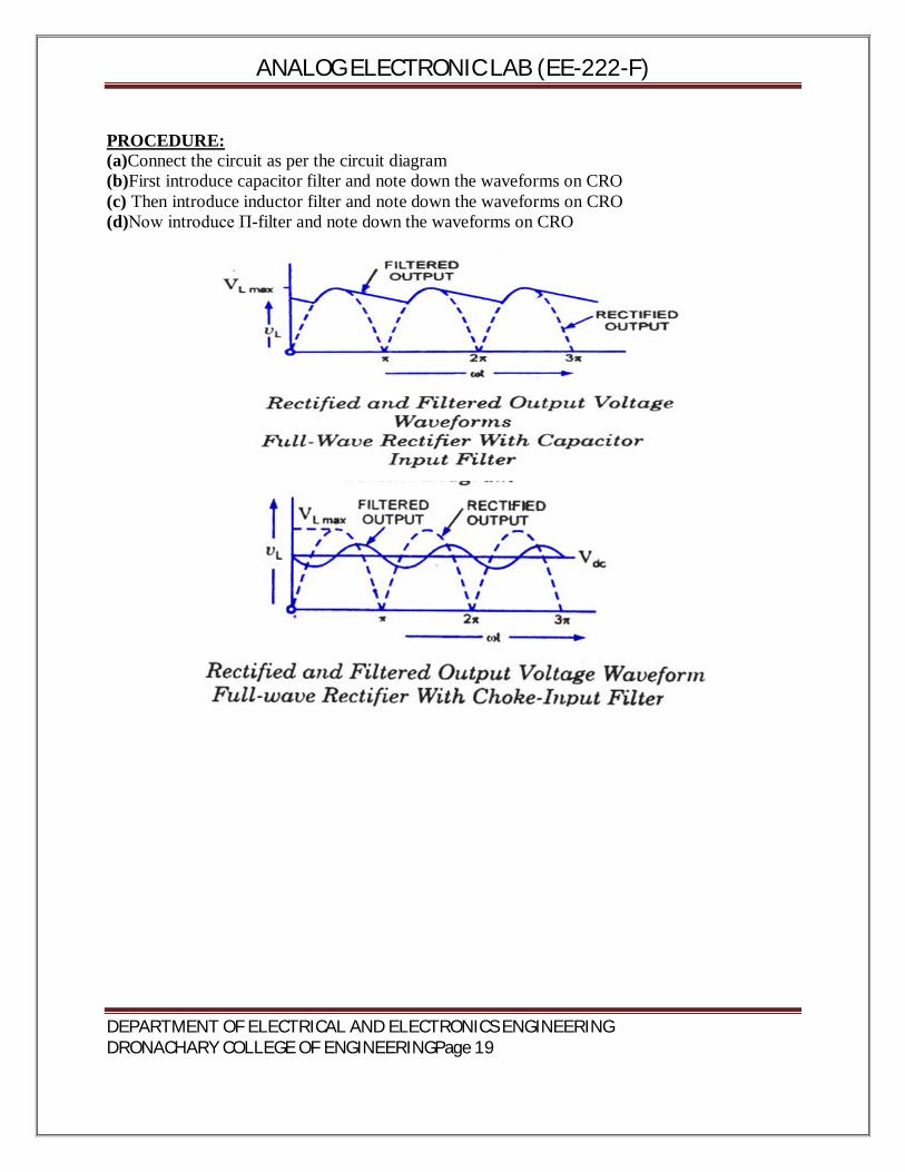
PROCEDURE: (a)Connect the circuit as per the circuit diagram (b)First introduce capacitor filter and note down the waveforms on CRO (c) Then introduce inductor filter and note down the waveforms on CRO (d)Now introduce П-filter and note down the waveforms on CRO
ANALOG ELECTRONIC LAB (EE-222-F)
DEPARTMENT OF ELECTRICAL AND ELECTRONICS ENGINEERING DRONACHARY COLLEGE OF ENGINEERINGPage 20
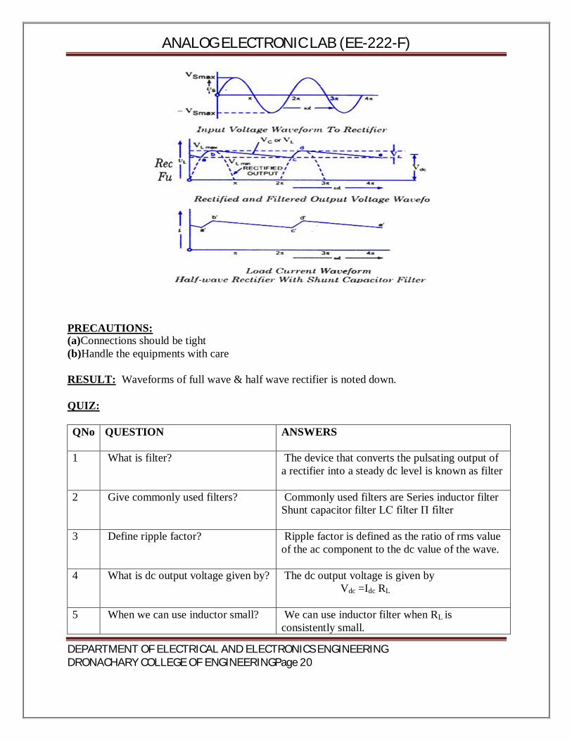
PRECAUTIONS: (a)Connections should be tight (b)Handle the equipments with care RESULT: Waveforms of full wave & half wave rectifier is noted down. QUIZ: QNo QUESTION ANSWERS
1 What is filter? The device that converts the pulsating output of
a rectifier into a steady dc level is known as filter
2 Give commonly used filters?
Commonly used filters are Series inductor filter Shunt capacitor filter LC filter П filter
3 Define ripple factor?
Ripple factor is defined as the ratio of rms value of the ac component to the dc value of the wave.
4 What is dc output voltage given by?
The dc output voltage is given by Vdc =Idc RL
5 When we can use inductor small?
We can use inductor filter when RL is consistently small.
ANALOG ELECTRONIC LAB (EE-222-F)
DEPARTMENT OF ELECTRICAL AND ELECTRONICS ENGINEERING DRONACHARY COLLEGE OF ENGINEERINGPage 21
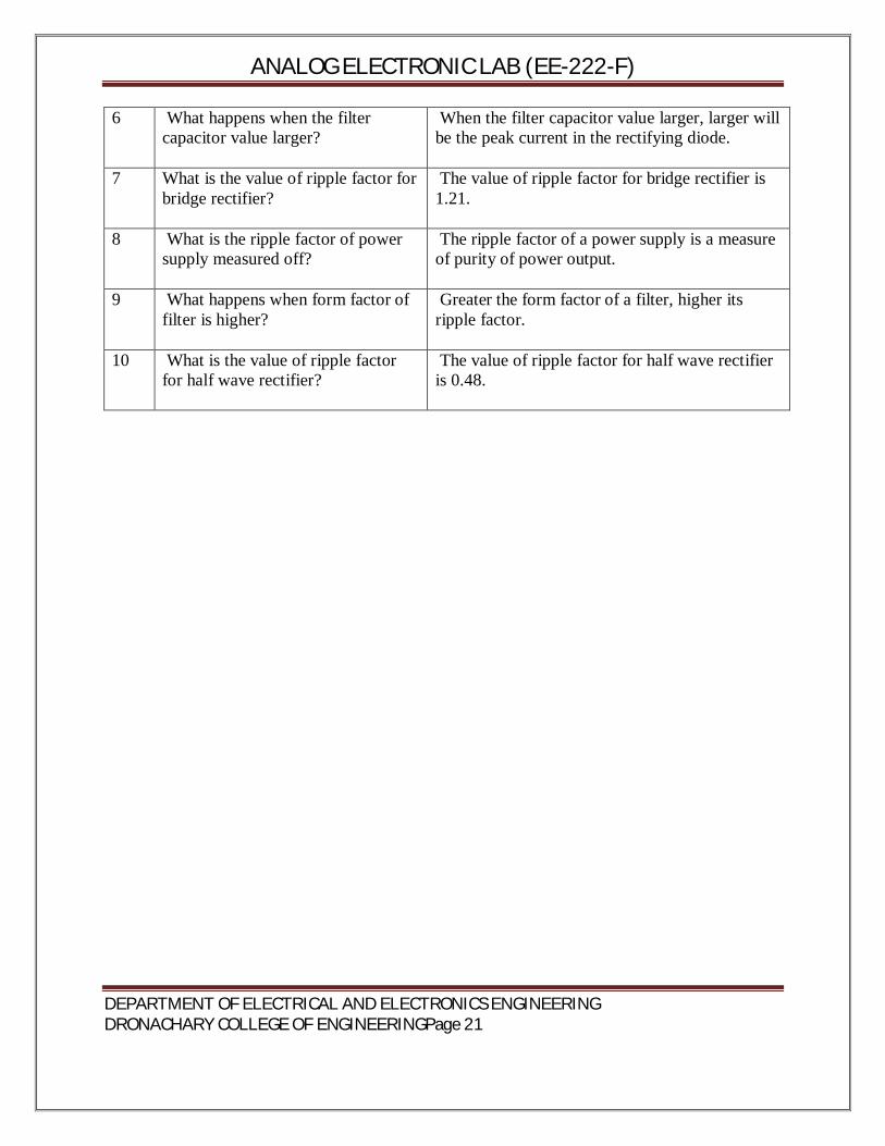
6 What happens when the filter capacitor value larger?
When the filter capacitor value larger, larger will be the peak current in the rectifying diode.
7 What is the value of ripple factor for bridge rectifier?
The value of ripple factor for bridge rectifier is 1.21.
8 What is the ripple factor of power supply measured off?
The ripple factor of a power supply is a measure of purity of power output.
9 What happens when form factor of filter is higher?
Greater the form factor of a filter, higher its ripple factor.
10 What is the value of ripple factor for half wave rectifier?
The value of ripple factor for half wave rectifier is 0.48.
ANALOG ELECTRONIC LAB (EE-222-F)
DEPARTMENT OF ELECTRICAL AND ELECTRONICS ENGINEERING DRONACHARY COLLEGE OF ENGINEERINGPage 22
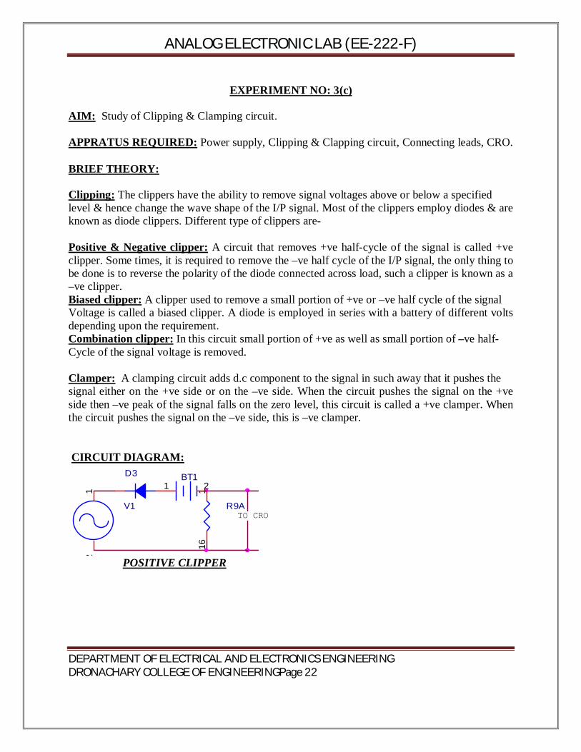
EXPERIMENT NO: 3(c)
AIM: Study of Clipping & Clamping circuit. APPRATUS REQUIRED: Power supply, Clipping & Clapping circuit, Connecting leads, CRO. BRIEF THEORY: Clipping: The clippers have the ability to remove signal voltages above or below a specified level & hence change the wave shape of the I/P signal. Most of the clippers employ diodes & are known as diode clippers. Different type of clippers are- Positive & Negative clipper: A circuit that removes +ve half-cycle of the signal is called +ve clipper. Some times, it is required to remove the –ve half cycle of the I/P signal, the only thing to be done is to reverse the polarity of the diode connected across load, such a clipper is known as a –ve clipper. Biased clipper: A clipper used to remove a small portion of +ve or –ve half cycle of the signal Voltage is called a biased clipper. A diode is employed in series with a battery of different volts depending upon the requirement. Combination clipper: In this circuit small portion of +ve as well as small portion of –ve half- Cycle of the signal voltage is removed. Clamper: A clamping circuit adds d.c component to the signal in such away that it pushes the signal either on the +ve side or on the –ve side. When the circuit pushes the signal on the +ve side then –ve peak of the signal falls on the zero level, this circuit is called a +ve clamper. When the circuit pushes the signal on the –ve side, this is –ve clamper. CIRCUIT DIAGRAM:
D3
TO CROR9A
116
V1
12
BT11 2
POSITIVE CLIPPER
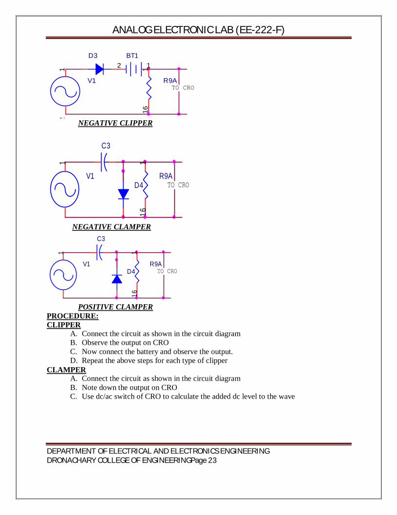
ANALOG ELECTRONIC LAB (EE-222-F)
DEPARTMENT OF ELECTRICAL AND ELECTRONICS ENGINEERING DRONACHARY COLLEGE OF ENGINEERINGPage 23
D3
TO CROR9A
116
V1
12
BT112
NEGATIVE CLIPPER
TO CROR9A
116
V1
12
D4
C3
NEGATIVE CLAMPER
TO CROR9A
116
V1
12
D4
C3
POSITIVE CLAMPER PROCEDURE: CLIPPER
A. Connect the circuit as shown in the circuit diagram B. Observe the output on CRO C. Now connect the battery and observe the output. D. Repeat the above steps for each type of clipper
CLAMPER A. Connect the circuit as shown in the circuit diagram B. Note down the output on CRO C. Use dc/ac switch of CRO to calculate the added dc level to the wave
ANALOG ELECTRONIC LAB (EE-222-F)
DEPARTMENT OF ELECTRICAL AND ELECTRONICS ENGINEERING DRONACHARY COLLEGE OF ENGINEERINGPage 24
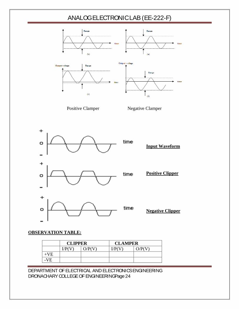
Positive Clamper Negative Clamper
Input Waveform Positive Clipper Negative Clipper
OBSERVATION TABLE:
CLIPPER CLAMPER I/P(V) O/P(V) I/P(V) O/P(V) +VE -VE
ANALOG ELECTRONIC LAB (EE-222-F)
DEPARTMENT OF ELECTRICAL AND ELECTRONICS ENGINEERING DRONACHARY COLLEGE OF ENGINEERINGPage 25
PRECAUTIONS:
A. Connection should be proper & tight. B. Switch ‘ON’ the supply after completing the circuit C. Handle the equipments with care
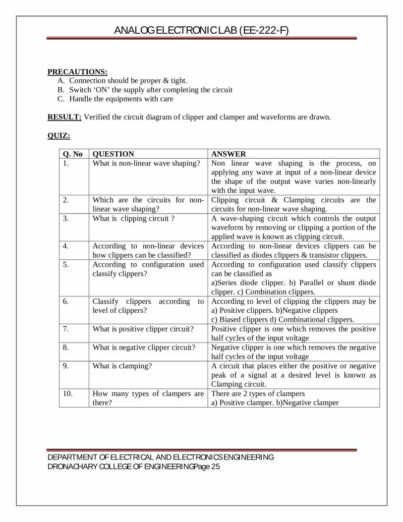
RESULT: Verified the circuit diagram of clipper and clamper and waveforms are drawn. QUIZ:
Q. No QUESTION ANSWER 1. What is non-linear wave shaping? Non linear wave shaping is the process, on
applying any wave at input of a non-linear device the shape of the output wave varies non-linearly with the input wave.
2. Which are the circuits for non-linear wave shaping?
Clipping circuit & Clamping circuits are the circuits for non-linear wave shaping.
3. What is clipping circuit ? A wave-shaping circuit which controls the output waveform by removing or clipping a portion of the applied wave is known as clipping circuit.
4. According to non-linear devices how clippers can be classified?
According to non-linear devices clippers can be classified as diodes clippers & transistor clippers.
5. According to configuration used classify clippers?
According to configuration used classify clippers can be classified as a)Series diode clipper. b) Parallel or shunt diode clipper. c) Combination clippers.
6. Classify clippers according to level of clippers?
According to level of clipping the clippers may be a) Positive clippers. b)Negative clippers c) Biased clippers d) Combinational clippers.
7. What is positive clipper circuit? Positive clipper is one which removes the positive half cycles of the input voltage
8. What is negative clipper circuit? Negative clipper is one which removes the negative half cycles of the input voltage
9. What is clamping? A circuit that places either the positive or negative peak of a signal at a desired level is known as Clamping circuit.
10. How many types of clampers are there?
There are 2 types of clampers a) Positive clamper. b)Negative clamper
ANALOG ELECTRONIC LAB (EE-222-F)
DEPARTMENT OF ELECTRICAL AND ELECTRONICS ENGINEERING DRONACHARY COLLEGE OF ENGINEERINGPage 26
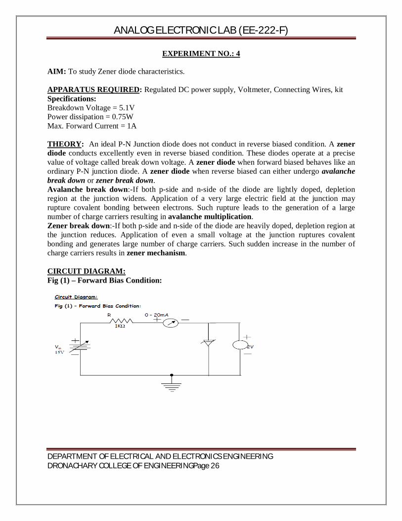
EXPERIMENT NO.: 4
AIM: To study Zener diode characteristics. APPARATUS REQUIRED: Regulated DC power supply, Voltmeter, Connecting Wires, kit Specifications: Breakdown Voltage = 5.1V Power dissipation = 0.75W Max. Forward Current = 1A THEORY: An ideal P-N Junction diode does not conduct in reverse biased condition. A zener diode conducts excellently even in reverse biased condition. These diodes operate at a precise value of voltage called break down voltage. A zener diode when forward biased behaves like an ordinary P-N junction diode. A zener diode when reverse biased can either undergo avalanche break down or zener break down. Avalanche break down:-If both p-side and n-side of the diode are lightly doped, depletion region at the junction widens. Application of a very large electric field at the junction may rupture covalent bonding between electrons. Such rupture leads to the generation of a large number of charge carriers resulting in avalanche multiplication. Zener break down:-If both p-side and n-side of the diode are heavily doped, depletion region at the junction reduces. Application of even a small voltage at the junction ruptures covalent bonding and generates large number of charge carriers. Such sudden increase in the number of charge carriers results in zener mechanism. CIRCUIT DIAGRAM: Fig (1) – Forward Bias Condition:
ANALOG ELECTRONIC LAB (EE-222-F)
DEPARTMENT OF ELECTRICAL AND ELECTRONICS ENGINEERING DRONACHARY COLLEGE OF ENGINEERINGPage 27
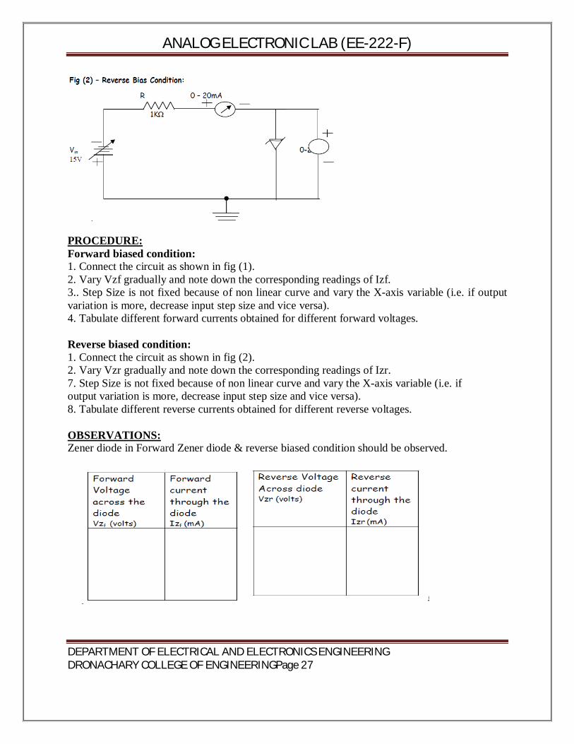
PROCEDURE: Forward biased condition: 1. Connect the circuit as shown in fig (1). 2. Vary Vzf gradually and note down the corresponding readings of Izf. 3.. Step Size is not fixed because of non linear curve and vary the X-axis variable (i.e. if output variation is more, decrease input step size and vice versa). 4. Tabulate different forward currents obtained for different forward voltages. Reverse biased condition: 1. Connect the circuit as shown in fig (2). 2. Vary Vzr gradually and note down the corresponding readings of Izr. 7. Step Size is not fixed because of non linear curve and vary the X-axis variable (i.e. if output variation is more, decrease input step size and vice versa). 8. Tabulate different reverse currents obtained for different reverse voltages. OBSERVATIONS: Zener diode in Forward Zener diode & reverse biased condition should be observed.
ANALOG ELECTRONIC LAB (EE-222-F)
DEPARTMENT OF ELECTRICAL AND ELECTRONICS ENGINEERING DRONACHARY COLLEGE OF ENGINEERINGPage 28
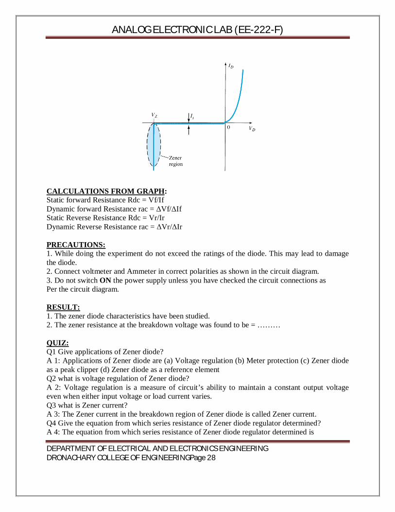
CALCULATIONS FROM GRAPH: Static forward Resistance Rdc = Vf/If Dynamic forward Resistance rac = ΔVf/ΔIf Static Reverse Resistance Rdc = Vr/Ir Dynamic Reverse Resistance rac = ΔVr/ΔIr PRECAUTIONS: 1. While doing the experiment do not exceed the ratings of the diode. This may lead to damage the diode. 2. Connect voltmeter and Ammeter in correct polarities as shown in the circuit diagram. 3. Do not switch ON the power supply unless you have checked the circuit connections as Per the circuit diagram. RESULT: 1. The zener diode characteristics have been studied. 2. The zener resistance at the breakdown voltage was found to be = ……… QUIZ: Q1 Give applications of Zener diode? A 1: Applications of Zener diode are (a) Voltage regulation (b) Meter protection (c) Zener diode as a peak clipper (d) Zener diode as a reference element Q2 what is voltage regulation of Zener diode? A 2: Voltage regulation is a measure of circuit’s ability to maintain a constant output voltage even when either input voltage or load current varies. Q3 what is Zener current? A 3: The Zener current in the breakdown region of Zener diode is called Zener current. Q4 Give the equation from which series resistance of Zener diode regulator determined? A 4: The equation from which series resistance of Zener diode regulator determined is
ANALOG ELECTRONIC LAB (EE-222-F)
DEPARTMENT OF ELECTRICAL AND ELECTRONICS ENGINEERING DRONACHARY COLLEGE OF ENGINEERINGPage 29
RS = VS-VOUT / IZMAX Where VS is source voltage, VOUT is output voltage & IZMAX is maximum current through Zener diode. Q5 Give advantages of Zener diode regulator over other regulators? A 5: Advantages of Zener diode regulator over other regulators are that they are smaller in size, lighter in weight and have longer life. Q6. What is Zener diode? A 6: Zener diode, also sometimes called the breakdown diode is a P-N junction diode specially designed for operation in the breakdown region in reverse bias condition. Q7 Give several methods used to manufacture of Zener diodes? A 7: several methods used to manufacture of Zener diodes are diffused structure, diffused and passivated structure and alloy diffused structure. Q8 In passivated structure of a Zener diode by which layer edges of the junction are covered? A 8: In passivated structure of a Zener diode; Silicon Dioxide layer edges of the junction are covered. Q9 Give the voltage range availability of Zener diodes? A 9: The voltage range availability of Zener diodes is 2.4v to 200v. Q10. What is Zener voltage? A 10: The voltage at which the Zener diode breaks down is called the Zener voltage.
ANALOG ELECTRONIC LAB (EE-222-F)
DEPARTMENT OF ELECTRICAL AND ELECTRONICS ENGINEERING DRONACHARY COLLEGE OF ENGINEERINGPage 30
EXPERIMENT NO.: 5 AIM: To study zener diode as voltage regulator. APPRATUS REQUIRED: Power Supply, Zener Diode, Two Voltmeter and connected leads Ammeter. BRIEF THEORY:- The Zener diode is operated in the breakdown or zener region, the voltage across it is substantially constant for a large current of current through it. This characteristic permits it to be used as a voltage regulator. As the lode Current increases, the Zener current decrease so that current through resistance Rs is constant. As out put voltage = Vin – Irs, and I is constant, Therefore, output Voltage remains unchanged. The input voltage Vin increase, more current will flow through the zener, the voltage drop across Rs will increase but lode voltage would remain constant. CIRCUIT DIAGRAM:
12
RL1
16
mA
V
1 16
0-15V
Vs
PROCEDURE: (a)Connect the circuit as per the circuit diagram (b)Keep load resistance constant (take maximum value of load resistance) (c)Vary input voltage and note down output voltage (d)Now keep input voltage constant and vary load resistance and note down corresponding voltmeter reading
(e)Plot the respective graph OBSERVATION TABLE:
S. No Vs( VOLT) V( VOLT) RL(E) V (VOLT) 1 2 3 4 5 6 7
ANALOG ELECTRONIC LAB (EE-222-F)
DEPARTMENT OF ELECTRICAL AND ELECTRONICS ENGINEERING DRONACHARY COLLEGE OF ENGINEERINGPage 31
8 9 10
PRECAUTIONS:
(a)Connections should be tight (b)Handle the equipments with care RESULT: Studied how Zener diode is used as a voltage regulator. QUIZ: QNo QUESTION ANSWERS 1 Give applications of Zener diode? Applications of Zener diode are
(a) Voltage regulation (b) Meter protection (c) Zener diode as a peak clipper (d) Zener diode as a reference element
2 What is voltage regulation of Zener diode?
Voltage regulation is a measure of circuit’s ability to maintain a constant output voltage even when either input voltage or load current varies.
3 What is Zener current? The Zener current in the breakdown region of Zener diode is called Zener current.
4 Give the equation from which series resistance of Zener diode regulator determined?
The equation from which series resistance of Zener diode regulator determined is
RS = VS-VOUT / IZMAX WhereVS is source voltage,VOUT is output voltage & IZMAX is
maximum current through Zener diode. 5 Give advantages of Zener diode
regulator over other regulators? Advantages of Zener diode regulator over other regulators are that they are smaller in size, lighter in weight and have longer life.
6 What is Zener diode? Zener diode, also sometimes called the breakdown diode ia a P-N junction diode specially designed for operation in the breakdown region in reverse bias condition.
7 Give several methods used to manufacture of Zener diodes?
several methods used to manufacture of Zener diodes are diffused structure, diffused and passivated structure and alloy diffused structure.
8 In passivated structure of a Zener diode by which layer edges of the junction are covered?
In passivated structure of a Zener diode; Silicon Dioxide layer edges of the junction are covered.
9 Give the voltage range availability of Zener diodes?
The voltage range availability of Zener diodes is 2.4v to 200v.
10 What is Zener voltage?
The voltage at which the Zener diode breaks down is called the Zener voltage.
ANALOG ELECTRONIC LAB (EE-222-F)
DEPARTMENT OF ELECTRICAL AND ELECTRONICS ENGINEERING DRONACHARY COLLEGE OF ENGINEERINGPage 32
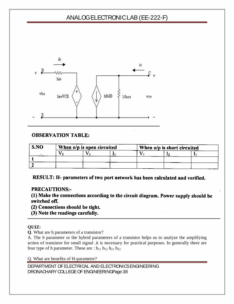
EXPERIMENT NO: 6(a)
AIM: To Study the characteristics of transistor in Common Base configuration. APPARATUS REQUIRED : Power supply, Transistor characteristics Kit, Connecting Leads, Voltmeter, Ammeter. BRIEF THEORY : Transistor is a semiconductor device consist of two p-n junctions. It has three terminals, to handle I/P and O/P four terminals are needed. Therefore, one terminal is made common. A transistor can be connected in three Ways CB, CE, and CC. Common base: Base is made common. I/P is connected between base & emitter and O/P is taken between base & collector. Input charact. The curve plotted between emitter current I & the emitter-base voltage constant collector-base voltage V. Output charact. The curve plotted between collector current I & collector-base voltage V constant emitter current I. . CIRCUIT DIAGRAM :
PROCEDURE: Input charact.
(a) Make the connection as per circuit diagram . (b) Switch ‘ON’ the supply & set V = 0V (c) Vary V in step & note down the emitter current I at each step . (d) Set V = 1V & again repeat the same procedure . (e) Draw the graph.
Output charact.
(a) Make the connection as per circuit diagram. (b) Set the value of I = 1mA
ANALOG ELECTRONIC LAB (EE-222-F)
DEPARTMENT OF ELECTRICAL AND ELECTRONICS ENGINEERING DRONACHARY COLLEGE OF ENGINEERINGPage 33
(c) Vary V in step & note down the collector current I at each step. (d) Set I = 2mA & repeat the same procedure. (e) Draw the graph .
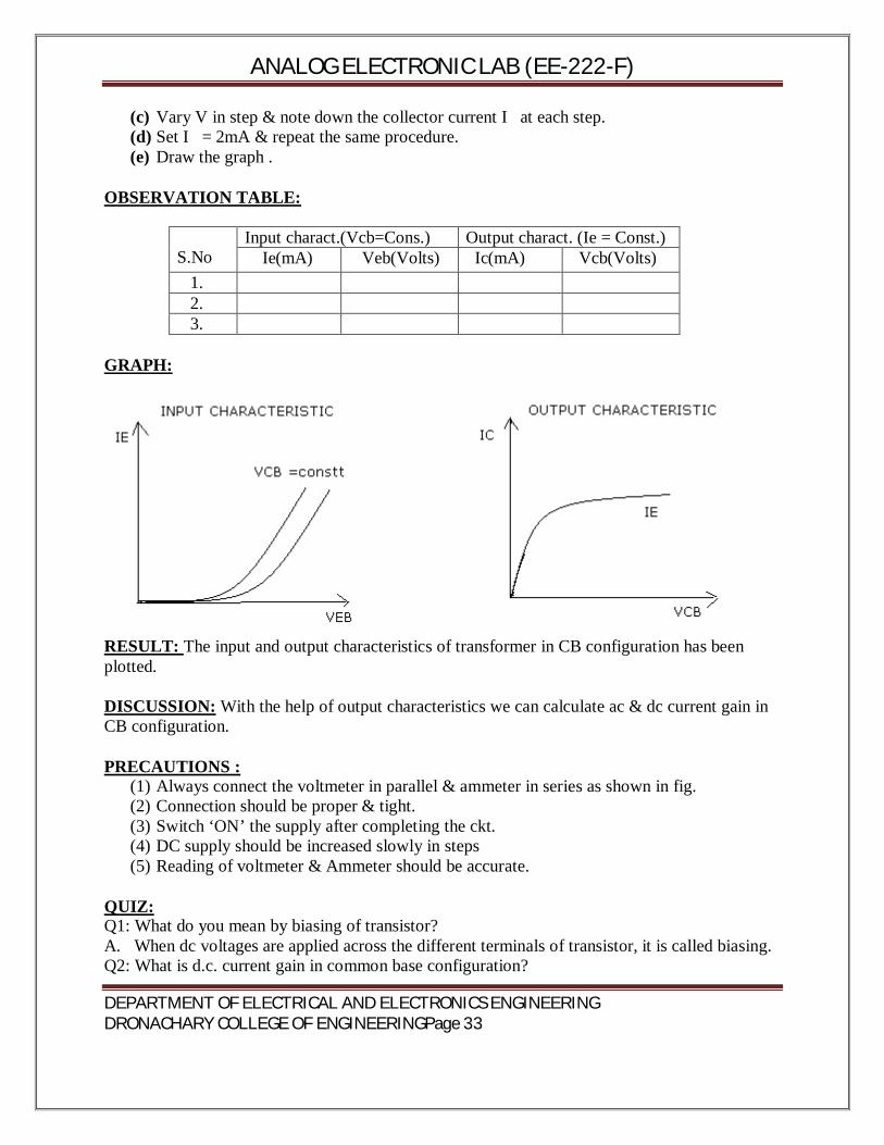
OBSERVATION TABLE:
S.No
Input charact.(Vcb=Cons.) Output charact. (Ie = Const.) Ie(mA) Veb(Volts) Ic(mA) Vcb(Volts)
1. 2. 3.
GRAPH:
RESULT: The input and output characteristics of transformer in CB configuration has been plotted. DISCUSSION: With the help of output characteristics we can calculate ac & dc current gain in CB configuration. PRECAUTIONS :
(1) Always connect the voltmeter in parallel & ammeter in series as shown in fig. (2) Connection should be proper & tight. (3) Switch ‘ON’ the supply after completing the ckt. (4) DC supply should be increased slowly in steps (5) Reading of voltmeter & Ammeter should be accurate.
QUIZ: Q1: What do you mean by biasing of transistor? A. When dc voltages are applied across the different terminals of transistor, it is called biasing. Q2: What is d.c. current gain in common base configuration?
ANALOG ELECTRONIC LAB (EE-222-F)
DEPARTMENT OF ELECTRICAL AND ELECTRONICS ENGINEERING DRONACHARY COLLEGE OF ENGINEERINGPage 34
A. It is ratio of collector current(Ic) to emitter current (Ie). Q3: What is typical value for d.c. current gain ? A. 0.99 Q4: What is a.c. current gain in CB confifuration? A. It is ratio of change in collector current to change in emitter current. Q5: What are input characteristics? A. These curves relate i/p current & i/p voltage for a given value of o/p voltage. Q6: What are output characteristics? A. Thes curves relate o/p voltage & o/p current for a given value of input current. Q7: Which configuration has highest voltage gain? A. Common Emitter. Q8: Which configuration is most widely used? A. Common Emitter. Q9: What is operating point? A. The zero signal values of Ic & Vce. Q10: Which reigon is heavily doped in Transistot? A. Emitter
ANALOG ELECTRONIC LAB (EE-222-F)
DEPARTMENT OF ELECTRICAL AND ELECTRONICS ENGINEERING DRONACHARY COLLEGE OF ENGINEERINGPage 35
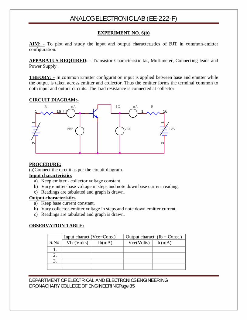
EXPERIMENT NO. 6(b) AIM: - To plot and study the input and output characteristics of BJT in common-emitter configuration. APPARATUS REQUIRED: - Transistor Characteristic kit, Multimeter, Connecting leads and Power Supply . THEORY: - In common Emitter configuration input is applied between base and emitter while the output is taken across emitter and collector. Thus the emitter forms the terminal common to doth input and output circuits. The load resistance is connected at collector. CIRCUIT DIAGRAM:-
R
12
12
VCE
R
12V
mA1 16
mAIC1 16
VBE
IB
PROCEDURE: (a)Connect the circuit as per the circuit diagram. Input characteristics
a) Keep emitter - collector voltage constant. b) Vary emitter-base voltage in steps and note down base current reading. c) Readings are tabulated and graph is drawn.
Output characteristics a) Keep base current constant. b) Vary collector-emitter voltage in steps and note down emitter current. c) Readings are tabulated and graph is drawn.
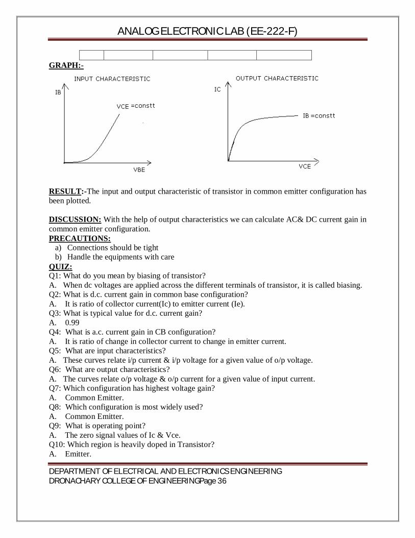
OBSERVATION TABLE:
S.No
Input charact.(Vce=Cons.) Output charact. (Ib = Const.) Vbe(Volts) Ib(mA) Vce(Volts) Ic(mA)
1. 2. 3.
ANALOG ELECTRONIC LAB (EE-222-F)
DEPARTMENT OF ELECTRICAL AND ELECTRONICS ENGINEERING DRONACHARY COLLEGE OF ENGINEERINGPage 36
GRAPH:-
RESULT:-The input and output characteristic of transistor in common emitter configuration has been plotted. DISCUSSION: With the help of output characteristics we can calculate AC& DC current gain in common emitter configuration. PRECAUTIONS:
a) Connections should be tight b) Handle the equipments with care
QUIZ: Q1: What do you mean by biasing of transistor? A. When dc voltages are applied across the different terminals of transistor, it is called biasing. Q2: What is d.c. current gain in common base configuration? A. It is ratio of collector current(Ic) to emitter current (Ie). Q3: What is typical value for d.c. current gain? A. 0.99 Q4: What is a.c. current gain in CB configuration? A. It is ratio of change in collector current to change in emitter current. Q5: What are input characteristics? A. These curves relate i/p current & i/p voltage for a given value of o/p voltage. Q6: What are output characteristics? A. The curves relate o/p voltage & o/p current for a given value of input current. Q7: Which configuration has highest voltage gain? A. Common Emitter. Q8: Which configuration is most widely used? A. Common Emitter. Q9: What is operating point? A. The zero signal values of Ic & Vce. Q10: Which region is heavily doped in Transistor? A. Emitter.
ANALOG ELECTRONIC LAB (EE-222-F)
DEPARTMENT OF ELECTRICAL AND ELECTRONICS ENGINEERING DRONACHARY COLLEGE OF ENGINEERINGPage 37
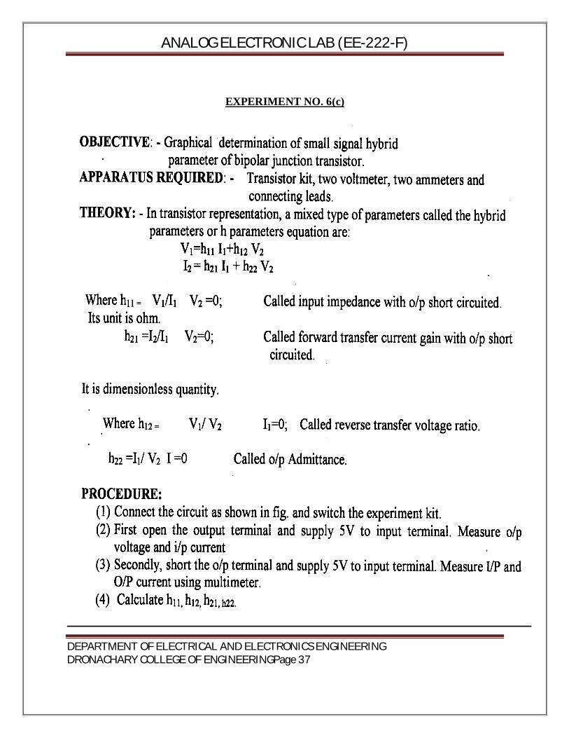
EXPERIMENT NO. 6(c)
ANALOG ELECTRONIC LAB (EE-222-F)
DEPARTMENT OF ELECTRICAL AND ELECTRONICS ENGINEERING DRONACHARY COLLEGE OF ENGINEERINGPage 38
QUIZ: Q. What are h parameters of a transistor? A. The h parameter or the hybrid parameters of a transistor helps us to analyze the amplifying action of transistor for small signal .it is necessary for practical purposes. In generally there are four type of h parameter. These are : h11 h12 h21 h22 Q. What are benefits of H-parameter?
ANALOG ELECTRONIC LAB (EE-222-F)
DEPARTMENT OF ELECTRICAL AND ELECTRONICS ENGINEERING DRONACHARY COLLEGE OF ENGINEERINGPage 39
A. Following are the advantages of h-parameters:- I. h-parameters are Real Numbers up to radio frequency
II. They are easy to measure III. They can be determined from transistor static characteristic curves IV. They are convenient to use in circuit analysis and design V. Easily convertible from one configuration to other
VI. Readily supplied by manufacturers Q. H parameter operates in which frequency? up to radio frequencies i.e 20-20khz Q. Which of the h-parameters corresponds to re in a common-base configuration? A. hib Q. Which of the following is referred to as the reverse transfer voltage ratio? A.hr Q.What is admittance? A. In electrical engineering, the admittance (Y) is a measure of how easily a circuit or device will allow a current to flow. It is defined as the inverse of the impedance (Z). The SI unit of admittance is the siemens (symbol S).
ANALOG ELECTRONIC LAB (EE-222-F)
DEPARTMENT OF ELECTRICAL AND ELECTRONICS ENGINEERING DRONACHARY COLLEGE OF ENGINEERINGPage 40
EXPERIMENT NO. : 7
AIM: To study and draw the characteristics of FET in common source configuration. APPRATUS REQUIRED: Power supply, FET characteristic Kit, connecting leads, two Multimeters. BRIEF THEORY: A FET is a three terminal semiconductor device in which current conduction is by one type of carries & is controlled by the effect of electric field. There are two types of FET namely JFET & MOSFET. Again, a JFET can either have N-channel or P-channel. A N-channel JFET has a N-type semiconductor bar, the two ends of which make the Drain & source terminal. On the two sides of this bar, P-N junction is made. This P region makes gate. Usually, these two gates are connected Together to form a single gate .The gate is given a –ve bias w.r.t source. The Drain is given +ve potential w.r.t source. CIRCUIT DIAGRAM:
D
12
12
VGS
mA
S
2
3
1
VDS
G
PROCEDURE: (a)Connect the circuit as per the circuit diagram Input characteristics (b)Keep drain-source voltage constant (c)Vary gate-source voltage in steps and note down drain current (d) Readings are tabulated and graph is drawn Output characteristics (a)Keep gate-source voltage constant (b)Vary drain-source voltage in steps and note down drain current. (c) Readings are tabulated and graph is drawn
ANALOG ELECTRONIC LAB (EE-222-F)
DEPARTMENT OF ELECTRICAL AND ELECTRONICS ENGINEERING DRONACHARY COLLEGE OF ENGINEERINGPage 41
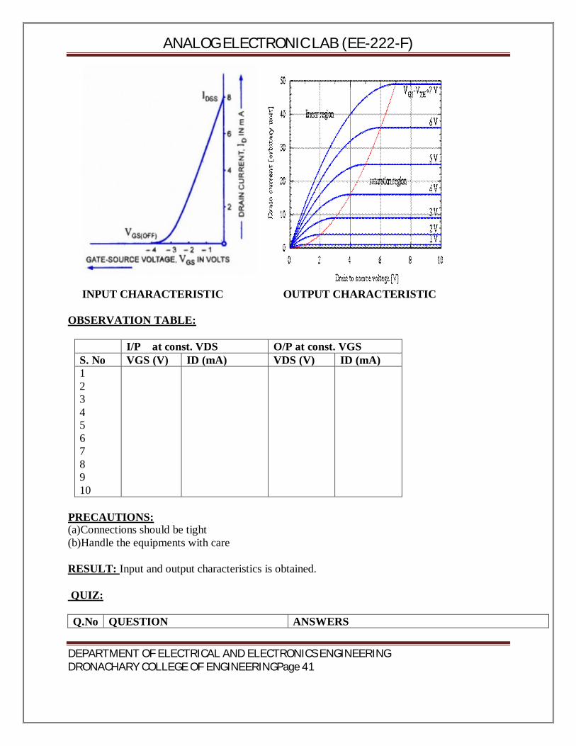
INPUT CHARACTERISTIC OUTPUT CHARACTERISTIC OBSERVATION TABLE:
I/P at const. VDS O/P at const. VGS S. No VGS (V) ID (mA) VDS (V) ID (mA) 1 2 3 4 5 6 7 8 9 10
PRECAUTIONS:
(a)Connections should be tight (b)Handle the equipments with care RESULT: Input and output characteristics is obtained. QUIZ: Q.No QUESTION ANSWERS
ANALOG ELECTRONIC LAB (EE-222-F)
DEPARTMENT OF ELECTRICAL AND ELECTRONICS ENGINEERING DRONACHARY COLLEGE OF ENGINEERINGPage 42
1 Define FET?
The field effect transistor is a semi-conductor device which depends for its operation on the control of current by an electric field.
2 How many types of FET’s are there? Two types (a) Junction field effect transistor (JFET). (b) Metal Oxide Semiconductor FET(MOSFET
3 Write advantages of FET over conventional Transistor?
Advantages are (a) Thermal stability. (b) Immunity to radiation (c) High input impedance.
4 Write one disadvantage of FET?
Main disadvantage is relatively small ‘Gain- Band Width ‘product.
5 Define Drain resistance? Drain resistance can be defined as ratio of drain to source voltage to drain current.
6 Define Tran conductance? Tran conductance can be defined as ratio of drain current to gate to source voltage.
7 Define transfer characteristic of FET?
The curve drawn between drain current and gate-source voltage for a given value of drain-source voltage.
8 Write applications of a FET?
Applications of FET are (A)Low noise amplifier (B) Buffer amplifier (C) Cascade amplifier (D) Analog switch (E)Chopper
9 How is Drain current controlled in JFET?
In JFET drain current is controlled by controlling the reverse bias given to its base.
10 Define pinch-off voltage?
The value of drain-source voltage at which channel is pinched off (i.e. all the free charges from the channel are removed) is called pinch-off voltage.
ANALOG ELECTRONIC LAB (EE-222-F)
DEPARTMENT OF ELECTRICAL AND ELECTRONICS ENGINEERING DRONACHARY COLLEGE OF ENGINEERINGPage 43
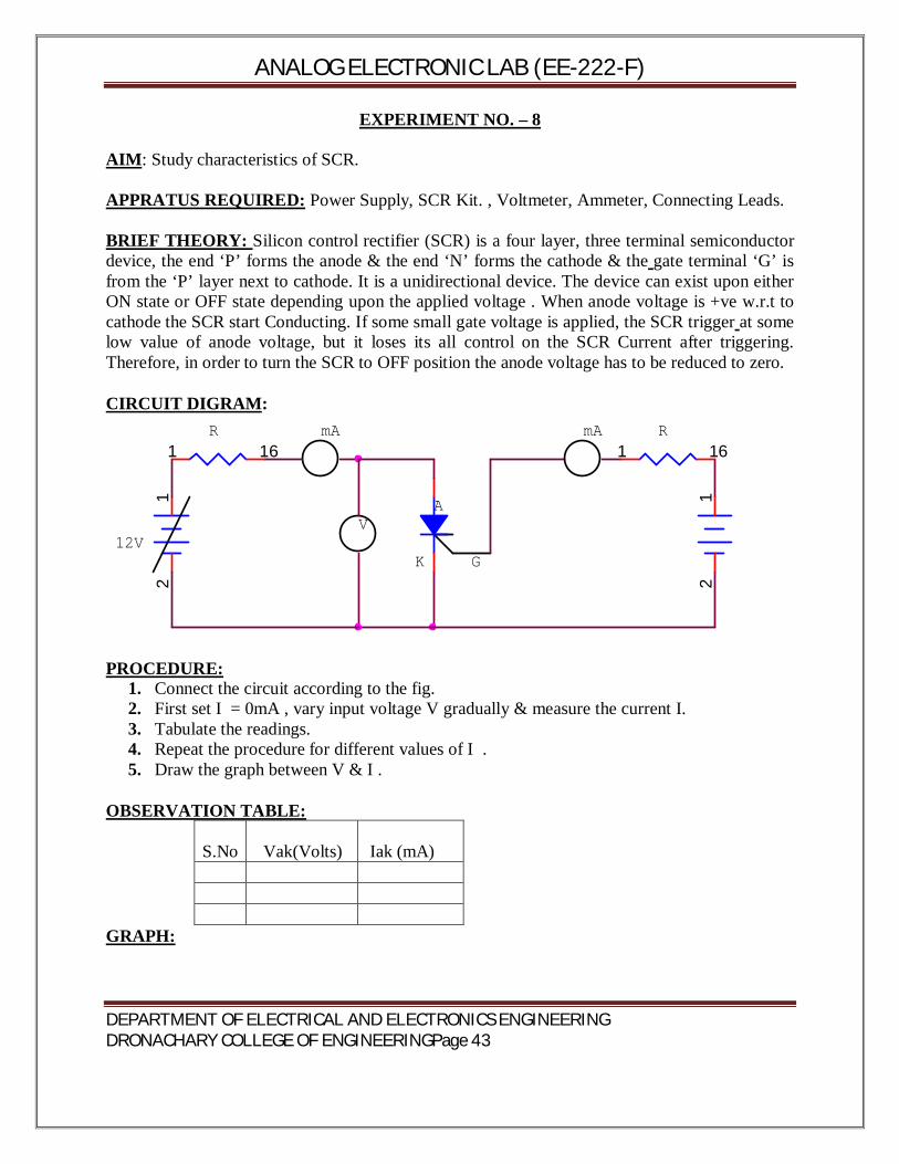
EXPERIMENT NO. – 8 AIM: Study characteristics of SCR. APPRATUS REQUIRED: Power Supply, SCR Kit. , Voltmeter, Ammeter, Connecting Leads. BRIEF THEORY: Silicon control rectifier (SCR) is a four layer, three terminal semiconductor device, the end ‘P’ forms the anode & the end ‘N’ forms the cathode & the gate terminal ‘G’ is from the ‘P’ layer next to cathode. It is a unidirectional device. The device can exist upon either ON state or OFF state depending upon the applied voltage . When anode voltage is +ve w.r.t to cathode the SCR start Conducting. If some small gate voltage is applied, the SCR trigger at some low value of anode voltage, but it loses its all control on the SCR Current after triggering. Therefore, in order to turn the SCR to OFF position the anode voltage has to be reduced to zero. CIRCUIT DIGRAM:
K G
12
mA
12V
12
1 16mA
A
R1 16
V
R
PROCEDURE:
1. Connect the circuit according to the fig. 2. First set I = 0mA , vary input voltage V gradually & measure the current I. 3. Tabulate the readings. 4. Repeat the procedure for different values of I . 5. Draw the graph between V & I .
OBSERVATION TABLE:
S.No
Vak(Volts)
Iak (mA)
GRAPH:
ANALOG ELECTRONIC LAB (EE-222-F)
DEPARTMENT OF ELECTRICAL AND ELECTRONICS ENGINEERING DRONACHARY COLLEGE OF ENGINEERINGPage 44
PRECAUTIONS:
1. Always connect the voltmeter in parallel & ammeter in series as shown in fig. 2. Connection should be proper & tight. 3. Switch ‘ON’ the supply after completing the circuit 4. DC supply should be increased slowly in steps 5. Reading of voltmeter & Ammeter should be accurate.
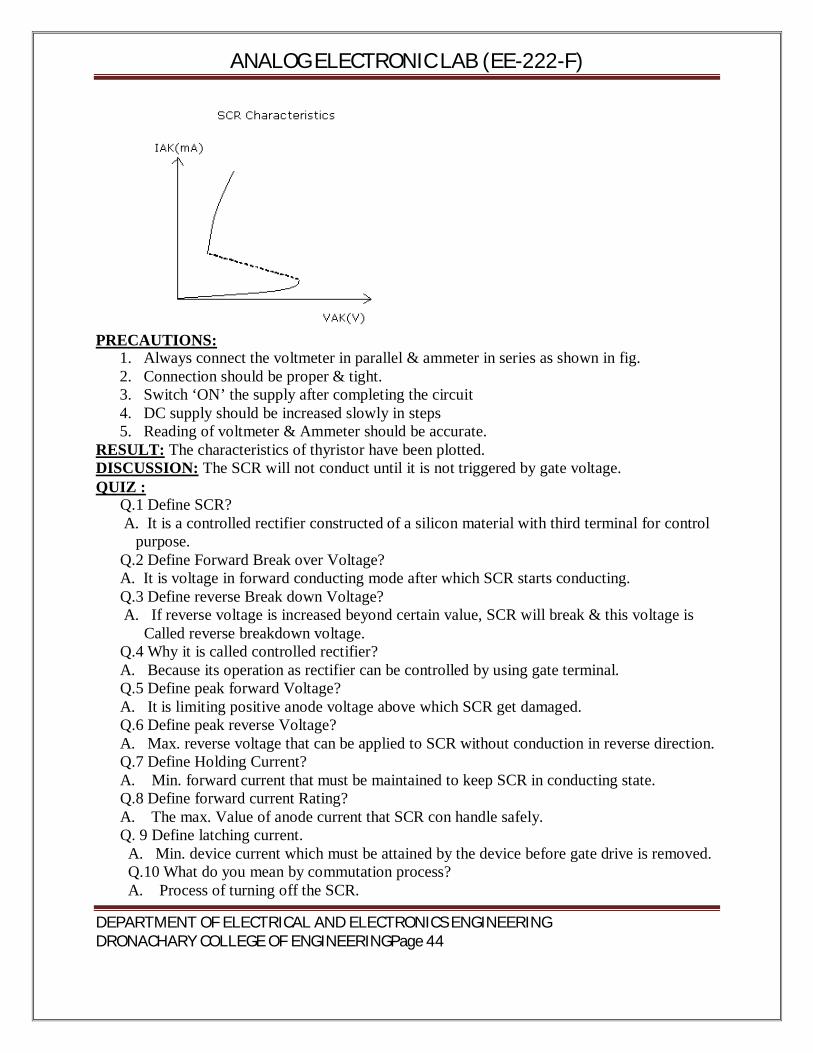
RESULT: The characteristics of thyristor have been plotted. DISCUSSION: The SCR will not conduct until it is not triggered by gate voltage. QUIZ : Q.1 Define SCR?
A. It is a controlled rectifier constructed of a silicon material with third terminal for control purpose.
Q.2 Define Forward Break over Voltage? A. It is voltage in forward conducting mode after which SCR starts conducting. Q.3 Define reverse Break down Voltage? A. If reverse voltage is increased beyond certain value, SCR will break & this voltage is Called reverse breakdown voltage. Q.4 Why it is called controlled rectifier? A. Because its operation as rectifier can be controlled by using gate terminal. Q.5 Define peak forward Voltage? A. It is limiting positive anode voltage above which SCR get damaged. Q.6 Define peak reverse Voltage? A. Max. reverse voltage that can be applied to SCR without conduction in reverse direction. Q.7 Define Holding Current? A. Min. forward current that must be maintained to keep SCR in conducting state. Q.8 Define forward current Rating? A. The max. Value of anode current that SCR con handle safely. Q. 9 Define latching current. A. Min. device current which must be attained by the device before gate drive is removed. Q.10 What do you mean by commutation process? A. Process of turning off the SCR.
ANALOG ELECTRONIC LAB (EE-222-F)
DEPARTMENT OF ELECTRICAL AND ELECTRONICS ENGINEERING DRONACHARY COLLEGE OF ENGINEERINGPage 45
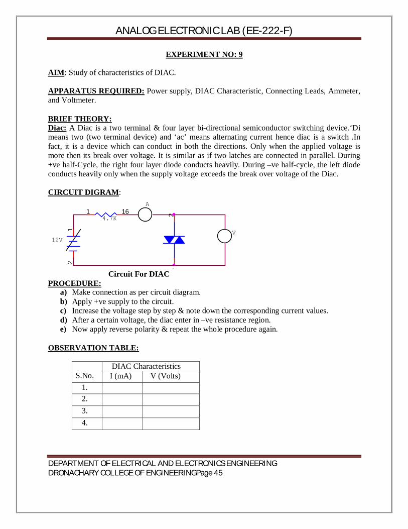
EXPERIMENT NO: 9 AIM: Study of characteristics of DIAC. APPARATUS REQUIRED: Power supply, DIAC Characteristic, Connecting Leads, Ammeter, and Voltmeter. BRIEF THEORY: Diac: A Diac is a two terminal & four layer bi-directional semiconductor switching device.‘Di means two (two terminal device) and ‘ac’ means alternating current hence diac is a switch .In fact, it is a device which can conduct in both the directions. Only when the applied voltage is more then its break over voltage. It is similar as if two latches are connected in parallel. During +ve half-Cycle, the right four layer diode conducts heavily. During –ve half-cycle, the left diode conducts heavily only when the supply voltage exceeds the break over voltage of the Diac. CIRCUIT DIGRAM:
A
12
12V
4.7K
12
1 16
V
Circuit For DIAC PROCEDURE:
a) Make connection as per circuit diagram. b) Apply +ve supply to the circuit. c) Increase the voltage step by step & note down the corresponding current values. d) After a certain voltage, the diac enter in –ve resistance region. e) Now apply reverse polarity & repeat the whole procedure again.
OBSERVATION TABLE:
S.No.
DIAC Characteristics I (mA) V (Volts)
1. 2. 3. 4.
ANALOG ELECTRONIC LAB (EE-222-F)
DEPARTMENT OF ELECTRICAL AND ELECTRONICS ENGINEERING DRONACHARY COLLEGE OF ENGINEERINGPage 46
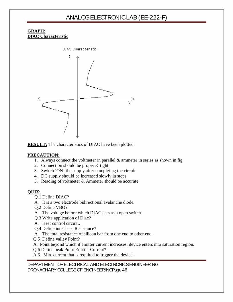
GRAPH: DIAC Characteristic
RESULT: The characteristics of DIAC have been plotted. PRECAUTION:
1. Always connect the voltmeter in parallel & ammeter in series as shown in fig. 2. Connection should be proper & tight. 3. Switch ‘ON’ the supply after completing the circuit 4. DC supply should be increased slowly in steps 5. Reading of voltmeter & Ammeter should be accurate.
QUIZ: Q.1 Define DIAC? A. It is a two electrode bidirectional avalanche diode. Q.2 Define VBO? A. The voltage before which DIAC acts as a open switch. Q.3 Write application of Diac? A. Heat control circuit.. Q.4 Define inter base Resistance? A. The total resistance of silicon bar from one end to other end. Q.5 Define valley Point?
A. Point beyond which if emitter current increases, device enters into saturation region. Q.6 Define peak Point Emitter Current? A.6 Min. current that is required to trigger the device.
ANALOG ELECTRONIC LAB (EE-222-F)
DEPARTMENT OF ELECTRICAL AND ELECTRONICS ENGINEERING DRONACHARY COLLEGE OF ENGINEERINGPage 47
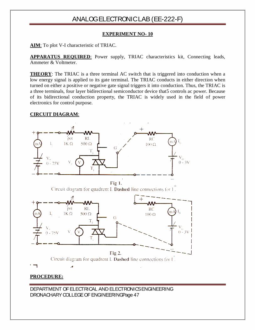
EXPERIMENT NO- 10 AIM: To plot V-I characteristic of TRIAC. APPARATUS REQUIRED: Power supply, TRIAC characteristics kit, Connecting leads, Ammeter & Voltmeter. THEORY: The TRIAC is a three terminal AC switch that is triggered into conduction when a low energy signal is applied to its gate terminal. The TRIAC conducts in either direction when turned on either a positive or negative gate signal triggers it into conduction. Thus, the TRIAC is a three terminals, four layer bidirectional semiconductor device that5 controls ac power. Because of its bidirectional conduction property, the TRIAC is widely used in the field of power electronics for control purpose. CIRCUIT DIAGRAM:
PROCEDURE:
ANALOG ELECTRONIC LAB (EE-222-F)
DEPARTMENT OF ELECTRICAL AND ELECTRONICS ENGINEERING DRONACHARY COLLEGE OF ENGINEERINGPage 48
(a) Make connection as per the circuit diagram. (b) Apply +ve supply to the circuit. (c) Increase the voltage step by step & note down the corresponding current values. (d) After a certain voltage, the TRIAC enters into the negative resistance region. (e) Now apply reserve polarity & repeat the whole procedure again.
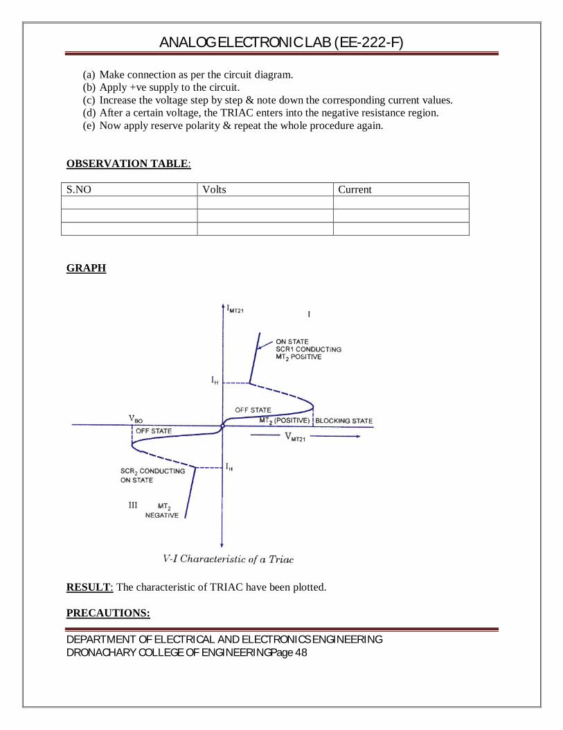
OBSERVATION TABLE: S.NO Volts Current GRAPH
RESULT: The characteristic of TRIAC have been plotted. PRECAUTIONS:
ANALOG ELECTRONIC LAB (EE-222-F)
DEPARTMENT OF ELECTRICAL AND ELECTRONICS ENGINEERING DRONACHARY COLLEGE OF ENGINEERINGPage 49
(a) Always connect the voltmeter in parallel & ammeter in series. (b) Connection should be proper & tight. (c) Switch ‘on’ the supply after completing the circuit. (d) DC supply should be increased slowly in steps. (e) Reading of voltmeter & ammeter should be accurate.
QUIZ/ANSWER: Q-1 Conduction take place in triac is bidirectional or unidirectional? Ans: Bidirectional. Q-2 Expanded form of the word abbreviated TRIAC ? Ans Triode and AC. Q-3 Name three terminal of TRIAc? Ans Main Terminal 1(MT1) ,Main Terminal 2 (MT2) and Gate ‘G’. Q-4 What are the ratings of TRIAC available in market? Ans Voltage 1200 and Current 300A(rms). Q-5 Give application of TRIAC? Ans TRIACS are extensively used in :-
A. Residential lamp –dimmers. B. Heat control C. Speed control of small single phase series and induction motor.
Q-6 Is TRIAc have a capability to work in rectifier mode? Ans: Yes Q-7 By what manner TRIAC is different from SCR? Ans 1. bidirectional conduction. 2. TRIAC is a combination of two SCRs connected in anti parallel. Q-8 How many layers are there in TRIAc? Ans 5 layers. Q-9 What is the symbol of TRIAC?
Ans Q-10 how TRIAC is differ from DIAC? Ans TRIAC have gate terminal and DIAc didn’t.
ANALOG ELECTRONIC LAB (EE-222-F)
DEPARTMENT OF ELECTRICAL AND ELECTRONICS ENGINEERING DRONACHARY COLLEGE OF ENGINEERINGPage 50
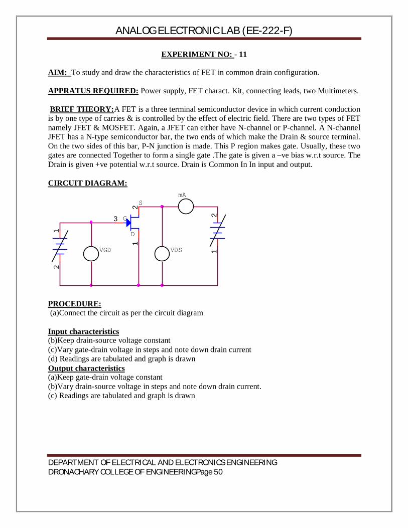
EXPERIMENT NO: - 11 AIM: To study and draw the characteristics of FET in common drain configuration. APPRATUS REQUIRED: Power supply, FET charact. Kit, connecting leads, two Multimeters. BRIEF THEORY:A FET is a three terminal semiconductor device in which current conduction is by one type of carries & is controlled by the effect of electric field. There are two types of FET namely JFET & MOSFET. Again, a JFET can either have N-channel or P-channel. A N-channel JFET has a N-type semiconductor bar, the two ends of which make the Drain & source terminal. On the two sides of this bar, P-N junction is made. This P region makes gate. Usually, these two gates are connected Together to form a single gate .The gate is given a –ve bias w.r.t source. The Drain is given +ve potential w.r.t source. Drain is Common In In input and output. CIRCUIT DIAGRAM:
D12
12
VGD
mAS2
3
1
VDS
G
PROCEDURE: (a)Connect the circuit as per the circuit diagram Input characteristics (b)Keep drain-source voltage constant (c)Vary gate-drain voltage in steps and note down drain current (d) Readings are tabulated and graph is drawn Output characteristics (a)Keep gate-drain voltage constant (b)Vary drain-source voltage in steps and note down drain current. (c) Readings are tabulated and graph is drawn
ANALOG ELECTRONIC LAB (EE-222-F)
DEPARTMENT OF ELECTRICAL AND ELECTRONICS ENGINEERING DRONACHARY COLLEGE OF ENGINEERINGPage 51
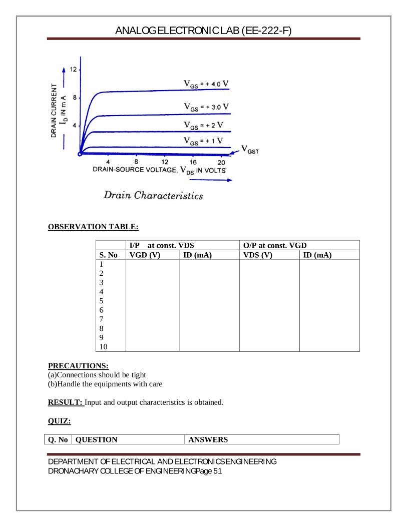
OBSERVATION TABLE:
I/P at const. VDS O/P at const. VGD S. No VGD (V) ID (mA) VDS (V) ID (mA) 1 2 3 4 5 6 7 8 9 10
PRECAUTIONS:
(a)Connections should be tight (b)Handle the equipments with care RESULT: Input and output characteristics is obtained. QUIZ: Q. No QUESTION ANSWERS
ANALOG ELECTRONIC LAB (EE-222-F)
DEPARTMENT OF ELECTRICAL AND ELECTRONICS ENGINEERING DRONACHARY COLLEGE OF ENGINEERINGPage 52
1 Which is the common log in common drain FET amplifier Between input and output.
Drain leg is common between input and output.
2 Define Pinch off voltage. The value of drain–source voltage at which channel is pinched off (i.e. all the free charges from the channel are removed)is called pinch–off voltage
3 Write advantages of FET over conventional Transistor.
Advantages are (a) Thermal stability. (b) Immunity to radiation. (c) High input impedance.
4 How much is the gain of common drain FET amplifier?
Gain of common drain amplifier is less than unity.
5 Define Drain resistance. Drain resistance can be defined as ratio of drain to source voltage to drain current.
6 Define Tran conductance. Tran conductance can be defined as ratio of drain current to gate to source voltage
ANALOG ELECTRONIC LAB (EE-222-F)
DEPARTMENT OF ELECTRICAL AND ELECTRONICS ENGINEERING DRONACHARY COLLEGE OF ENGINEERINGPage 53
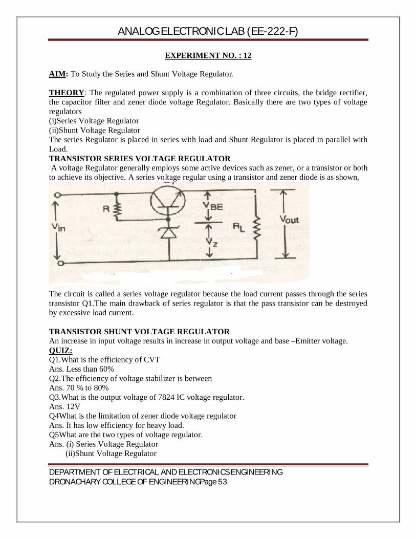
EXPERIMENT NO. : 12 AIM: To Study the Series and Shunt Voltage Regulator. THEORY: The regulated power supply is a combination of three circuits, the bridge rectifier, the capacitor filter and zener diode voltage Regulator. Basically there are two types of voltage regulators (i)Series Voltage Regulator (ii)Shunt Voltage Regulator The series Regulator is placed in series with load and Shunt Regulator is placed in parallel with Load. TRANSISTOR SERIES VOLTAGE REGULATOR A voltage Regulator generally employs some active devices such as zener, or a transistor or both to achieve its objective. A series voltage regular using a transistor and zener diode is as shown,
The circuit is called a series voltage regulator because the load current passes through the series transistor Q1.The main drawback of series regulator is that the pass transistor can be destroyed by excessive load current. TRANSISTOR SHUNT VOLTAGE REGULATOR An increase in input voltage results in increase in output voltage and base –Emitter voltage. QUIZ: Q1.What is the efficiency of CVT Ans. Less than 60% Q2.The efficiency of voltage stabilizer is between Ans. 70 % to 80% Q3.What is the output voltage of 7824 IC voltage regulator. Ans. 12V Q4What is the limitation of zener diode voltage regulator Ans. It has low efficiency for heavy load. Q5What are the two types of voltage regulator. Ans. (i) Series Voltage Regulator (ii)Shunt Voltage Regulator
ANALOG ELECTRONIC LAB (EE-222-F)
DEPARTMENT OF ELECTRICAL AND ELECTRONICS ENGINEERING DRONACHARY COLLEGE OF ENGINEERINGPage 54
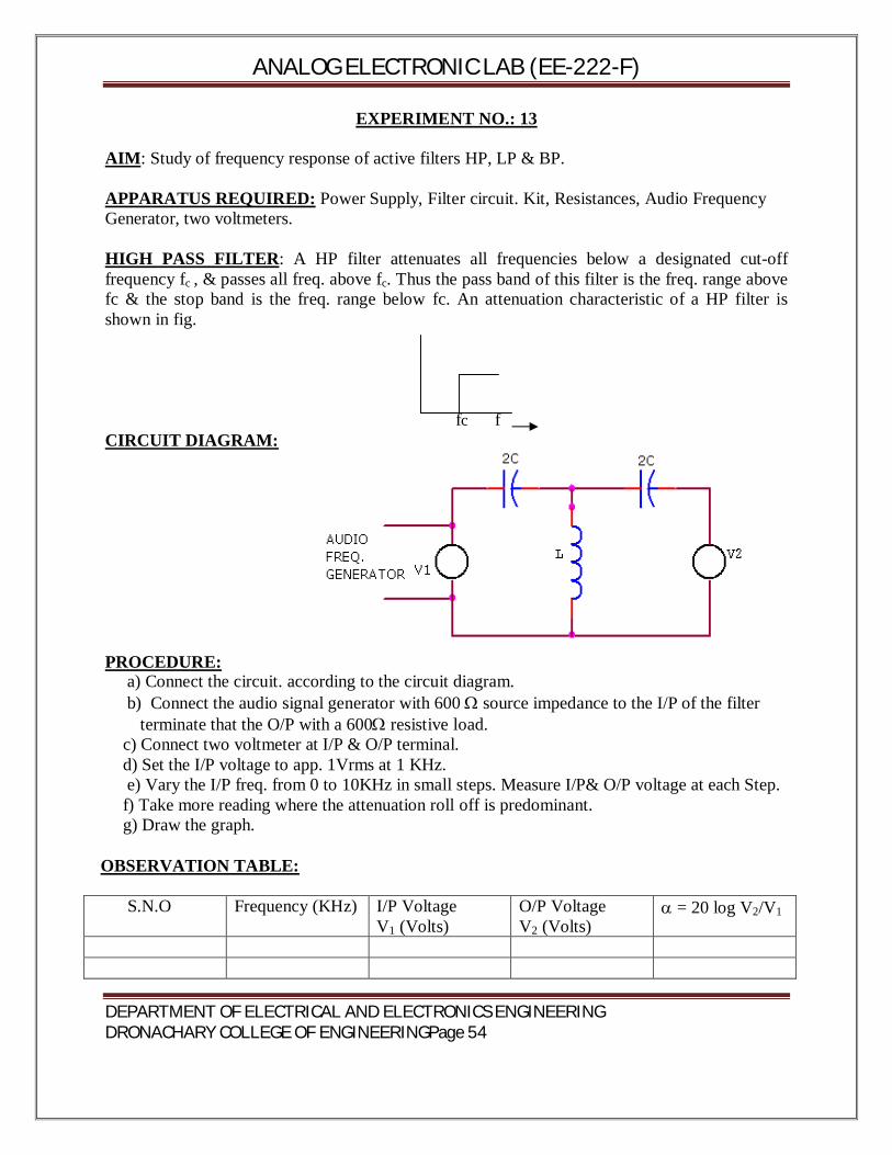
EXPERIMENT NO.: 13 AIM: Study of frequency response of active filters HP, LP & BP. APPARATUS REQUIRED: Power Supply, Filter circuit. Kit, Resistances, Audio Frequency Generator, two voltmeters. HIGH PASS FILTER: A HP filter attenuates all frequencies below a designated cut-off frequency fc , & passes all freq. above fc. Thus the pass band of this filter is the freq. range above fc & the stop band is the freq. range below fc. An attenuation characteristic of a HP filter is shown in fig.
fc f
CIRCUIT DIAGRAM:
PROCEDURE: a) Connect the circuit. according to the circuit diagram. b) Connect the audio signal generator with 600 source impedance to the I/P of the filter terminate that the O/P with a 600 resistive load. c) Connect two voltmeter at I/P & O/P terminal. d) Set the I/P voltage to app. 1Vrms at 1 KHz. e) Vary the I/P freq. from 0 to 10KHz in small steps. Measure I/P& O/P voltage at each Step. f) Take more reading where the attenuation roll off is predominant. g) Draw the graph.
OBSERVATION TABLE:
S.N.O Frequency (KHz) I/P Voltage V1 (Volts)
O/P Voltage V2 (Volts)
= 20 log V2/V1
ANALOG ELECTRONIC LAB (EE-222-F)
DEPARTMENT OF ELECTRICAL AND ELECTRONICS ENGINEERING DRONACHARY COLLEGE OF ENGINEERINGPage 55
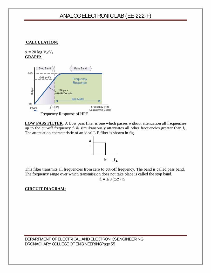
CALCULATION: = 20 log V2/V1 GRAPH:
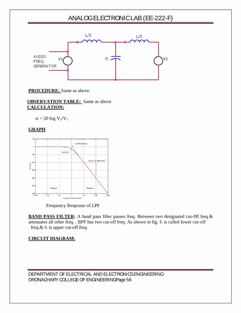
Frequency Response of HPF LOW PASS FILTER: A Low pass filter is one which passes without attenuation all frequencies up to the cut-off frequency fc & simultaneously attenuates all other frequencies greater than fc. The attenuation characteristic of an ideal L P filter is shown in fig. fc f This filter transmits all frequencies from zero to cut-off frequency. The band is called pass band. The frequency range over which transmission does not take place is called the stop band. fc = 1/ LC)½ CIRCUIT DIAGRAM:
ANALOG ELECTRONIC LAB (EE-222-F)
DEPARTMENT OF ELECTRICAL AND ELECTRONICS ENGINEERING DRONACHARY COLLEGE OF ENGINEERINGPage 56
PROCEDURE: Same as above.
OBSERVATION TABLE: Same as above CALCULATION: = 20 log V2/V1
GRAPH
Frequency Response of LPF BAND PASS FILTER: A band pass filter passes freq. Between two designated cut-0ff freq.& attenuates all other freq. . BPF has two cut-off freq. As shown in fig. f1 is called lower cut-off freq.& f2 is upper cut-off freq. CIRCUIT DIAGRAM:
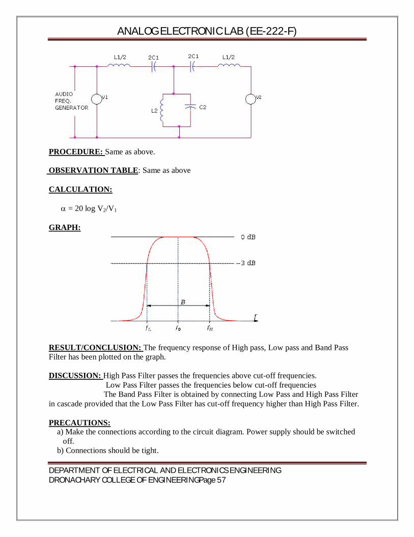
ANALOG ELECTRONIC LAB (EE-222-F)
DEPARTMENT OF ELECTRICAL AND ELECTRONICS ENGINEERING DRONACHARY COLLEGE OF ENGINEERINGPage 57
PROCEDURE: Same as above.
OBSERVATION TABLE: Same as above CALCULATION: = 20 log V2/V1 GRAPH:
RESULT/CONCLUSION: The frequency response of High pass, Low pass and Band Pass Filter has been plotted on the graph. DISCUSSION: High Pass Filter passes the frequencies above cut-off frequencies. Low Pass Filter passes the frequencies below cut-off frequencies The Band Pass Filter is obtained by connecting Low Pass and High Pass Filter in cascade provided that the Low Pass Filter has cut-off frequency higher than High Pass Filter.
PRECAUTIONS: a) Make the connections according to the circuit diagram. Power supply should be switched off. b) Connections should be tight.

ANALOG ELECTRONIC LAB (EE-222-F)
DEPARTMENT OF ELECTRICAL AND ELECTRONICS ENGINEERING DRONACHARY COLLEGE OF ENGINEERINGPage 58
c) Note the readings carefully. d) Take output carefully. e) Handle the CRO carefully. QUIZ/ANSWERS:
Q1 .Define Filter ?
A1. A filter is an electrical network that can transmit signals within a specified frequency range
Q2. Define Pass Band?
A2. The frequency range which is passed by the filter is called pass band
Q3. Define Stop Band? A3. The frequency range which is suppressed by the filter is called stop band.
Q4. Define Cut-Off frequency?
A4. The frequency that separates the pass band & attenuation band is known as the cut-off frequency.
Q5. Define High Pass Filter?
A5. A high pass filter attenuates all frequency below the cut-off frequency & allows to pass all other frequencies above the cut-off frequency
Q6. A high pass filter is one which a) passes all high freq. b)attenuates all low
freq. c)attenuates all freq. below designated cut-off freq. & passes all freq. above cut-off
A6. (c)
Q7. Where filter circuits are used ?
A7. Filter circuits are used in TV receivers, audio amplifiers etc
Q8.What are the units of attenuation? A8 . Decibles (dB) & Nepers. Q9. An ideal filter should have
a) Zero attenuation in the pass band b) Infinite attenuation in the pass band c) Zero attenuation in the attenuation band
A9. (a)
Q10.In the m-derived high pass filter, the resonant frequency is to be chosen so that it is a)Above the cut-off frequency b)Below the cut-off frequency c)None of the above
A10.(b)
Q11. Define Low Pass Filter?
A11.The low pass filter allows all frequencies up to the specified cut-off frequency to pass through it & attenuates all the other frequencies above the cut-off frequencies.
Q12. Define cut-off frequency?
A12. It demarcates the pass band & the stop band.
13. What is the freq. Range of Pass Band?
A13. The frequency range of pass band is from 0 to fc.
Q14. What is the freq. Range of Stop Band? A14. The frequency range of stop band is from
ANALOG ELECTRONIC LAB (EE-222-F)
DEPARTMENT OF ELECTRICAL AND ELECTRONICS ENGINEERING DRONACHARY COLLEGE OF ENGINEERINGPage 59
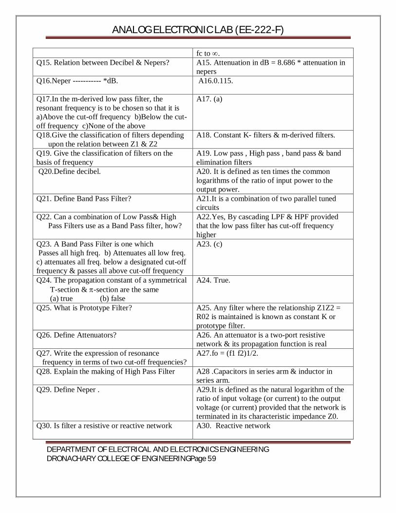
fc to . Q15. Relation between Decibel & Nepers?
A15. Attenuation in dB = 8.686 * attenuation in nepers
Q16.Neper ----------- *dB.
A16.0.115.
Q17.In the m-derived low pass filter, the resonant frequency is to be chosen so that it is a)Above the cut-off frequency b)Below the cut-off frequency c)None of the above
A17. (a)
Q18.Give the classification of filters depending upon the relation between Z1 & Z2
A18. Constant K- filters & m-derived filters.
Q19. Give the classification of filters on the basis of frequency
A19. Low pass , High pass , band pass & band elimination filters
Q20.Define decibel.
A20. It is defined as ten times the common logarithms of the ratio of input power to the output power.
Q21. Define Band Pass Filter?
A21.It is a combination of two parallel tuned circuits
Q22. Can a combination of Low Pass& High Pass Filters use as a Band Pass filter, how?
A22.Yes, By cascading LPF & HPF provided that the low pass filter has cut-off frequency higher
Q23. A Band Pass Filter is one which Passes all high freq. b) Attenuates all low freq. c) attenuates all freq. below a designated cut-off frequency & passes all above cut-off frequency
A23. (c)
Q24. The propagation constant of a symmetrical T-section & -section are the same (a) true (b) false
A24. True.
Q25. What is Prototype Filter?
A25. Any filter where the relationship Z1Z2 = R02 is maintained is known as constant K or prototype filter.
Q26. Define Attenuators?
A26. An attenuator is a two-port resistive network & its propagation function is real
Q27. Write the expression of resonance frequency in terms of two cut-off frequencies?
A27.fo = (f1 f2)1/2.
Q28. Explain the making of High Pass Filter A28 .Capacitors in series arm & inductor in series arm.
Q29. Define Neper .
A29.It is defined as the natural logarithm of the ratio of input voltage (or current) to the output voltage (or current) provided that the network is terminated in its characteristic impedance Z0.
Q30. Is filter a resistive or reactive network
A30. Reactive network
ANALOG ELECTRONIC LAB (EE-222-F)
DEPARTMENT OF ELECTRICAL AND ELECTRONICS ENGINEERING DRONACHARY COLLEGE OF ENGINEERINGPage 60