Embed Size (px)
Citation preview
4/11/2014 Seminar 1
T. R. Viswanathan
University of Texas at Austin
Analog Design Challenges in below 65nm CMOS
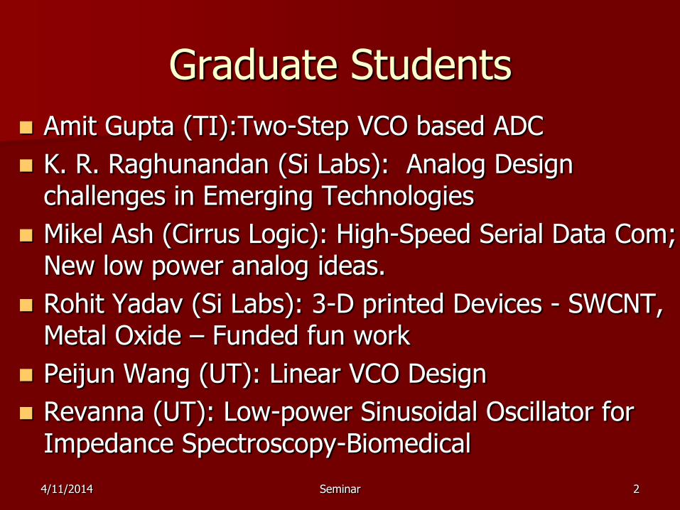
Graduate Students
Amit Gupta (TI):Two-Step VCO based ADC
K. R. Raghunandan (Si Labs): Analog Design challenges in Emerging Technologies
Mikel Ash (Cirrus Logic): High-Speed Serial Data Com; New low power analog ideas.
Rohit Yadav (Si Labs): 3-D printed Devices - SWCNT, Metal Oxide – Funded fun work
Peijun Wang (UT): Linear VCO Design
Revanna (UT): Low-power Sinusoidal Oscillator for Impedance Spectroscopy-Biomedical
4/11/2014 Seminar 2
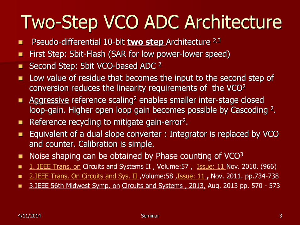
Two-Step VCO ADC Architecture Pseudo-differential 10-bit two step Architecture 2,3
First Step: 5bit-Flash (SAR for low power-lower speed)
Second Step: 5bit VCO-based ADC 2
Low value of residue that becomes the input to the second step of conversion reduces the linearity requirements of the VCO2
Aggressive reference scaling2 enables smaller inter-stage closed loop-gain. Higher open loop gain becomes possible by Cascoding 2.
Reference recycling to mitigate gain-error2.
Equivalent of a dual slope converter : Integrator is replaced by VCO and counter. Calibration is simple.
Noise shaping can be obtained by Phase counting of VCO3
1. IEEE Trans. on Circuits and Systems II , Volume:57 , Issue: 11 Nov. 2010. (966)
2.IEEE Trans. On Circuits and Sys. II ,Volume:58 ,Issue: 11 , Nov. 2011. pp.734-738
3.IEEE 56th Midwest Symp. on Circuits and Systems , 2013, Aug. 2013 pp. 570 - 573
4/11/2014 Seminar 3

Analog Design Challenges in
below 65nm CMOS High-speed Building Blocks (+,-,scale) using Class A-B CMOS
inverter: 6-bit resolution . Forget about op-amp and infinite-gain feedback at these speeds: Remember that the second world war was won without even the notion of an op-amp.
– Believe in this new mindset at these speeds. Think finite-Gain (2,4) with controlled feedback amplifiers for fast ADC. For example - Unity-Gain Buffer is a good starting point.
– Traditional use of a replica is not very effective because adjacent devices do not pretend to match. Multiplex the same device as replica when needed. Use S-C’s.
– Anti-alias Filter will need gm- control. Use V/I/T References
– We can do more energy-efficient ASP at GHz range
4/11/2014 Seminar 4

Transconductances
4/11/2014 Seminar 5
(b)
+
v
- gmv gmv
+
v
-
Transconductance Inverting
Transconductance
(a)
VSS
VSS
VDD
gmvv
VDD
v
VLT
gmv
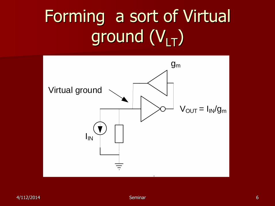
Forming a sort of Virtual ground (VLT)
4/112/2014 Seminar 6
gm
VOUT = IIN/gm
IIN
Virtual ground

Finite Voltage -Gain
4/11/2014 Seminar 7
2
1
2
1
VIN
VOUT = -VIN
VIN
VOUT = VIN
Voltage gain Av
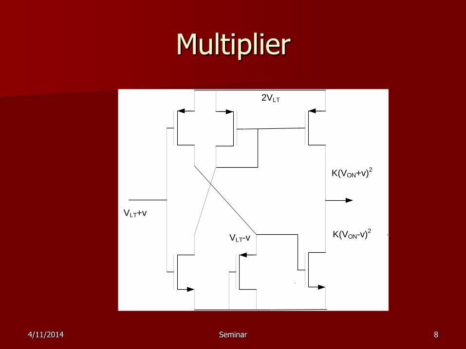
Multiplier
4/11/2014 Seminar 8
VLT+v
VLT-v
K(VON+v)2
K(VON-v)2
2VLT
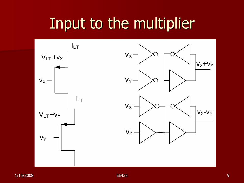
Input to the multiplier
1/15/2008 EE438 9
vX
vX
vY
vY
VLT +vX
vX
ILT
ILT
VLT +vY
vY
vX+vY
vX-vY
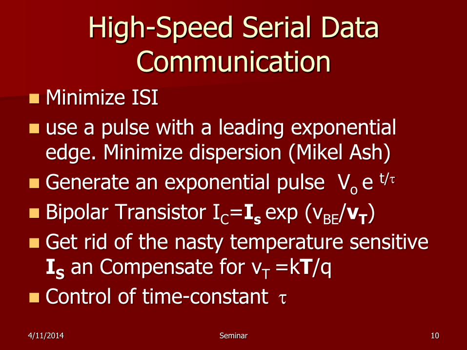
High-Speed Serial Data Communication
Minimize ISI
use a pulse with a leading exponential edge. Minimize dispersion (Mikel Ash)
Generate an exponential pulse Vo e t/t
Bipolar Transistor IC=Is exp (vBE/vT)
Get rid of the nasty temperature sensitive IS an Compensate for vT =kT/q
Control of time-constant t
4/11/2014 Seminar 10

Better BJT: IC= IREF exp(vIN/vT)
4/11/2014 Seminar 11
+ Vin
-
IREF
Ic= IREF exp (vin/vT)
vT ln(IREF/IS) + -
- vT
+
vT t/t
Ic= IS exp (vBE/vT)
+ VBE
_
VBE =Vin + vT ln(IREF/IS)
IS is gone!
PTAT Generator
IT
IC
T =nt

Impedance Spectroscopy
Identification of large molecules, DNA etc in liquid state. Also known as Cyclic Voltametry
Measure the real and imaginary parts of complex impedance.
Challenge: Low freq. resonance KHz to 5 MHz
Sinusoidal Oscillators: Sine and Cosine outputs
Hand held instruments like Blood Glucometer
Low-power :Throw away chip after a single test.
Two Designs are investigated, W-B and L-C
4/11/2014 Seminar 12
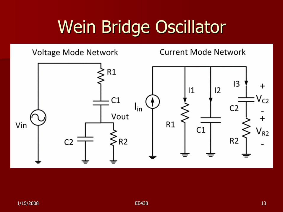
Wein Bridge Oscillator
1/15/2008 EE438 13
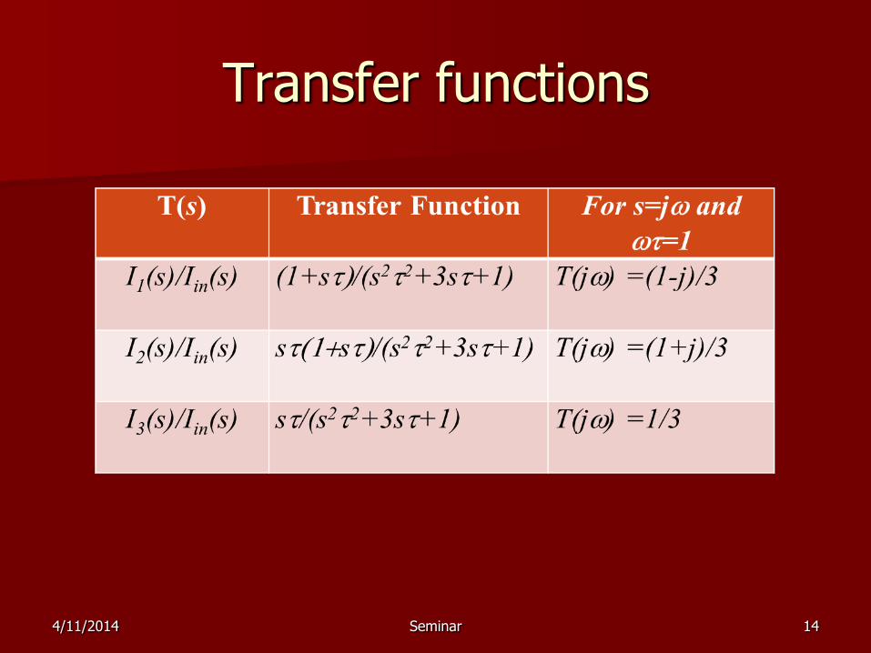
Transfer functions
4/11/2014 Seminar 14

Implementation
4/11/2014 Seminar 15
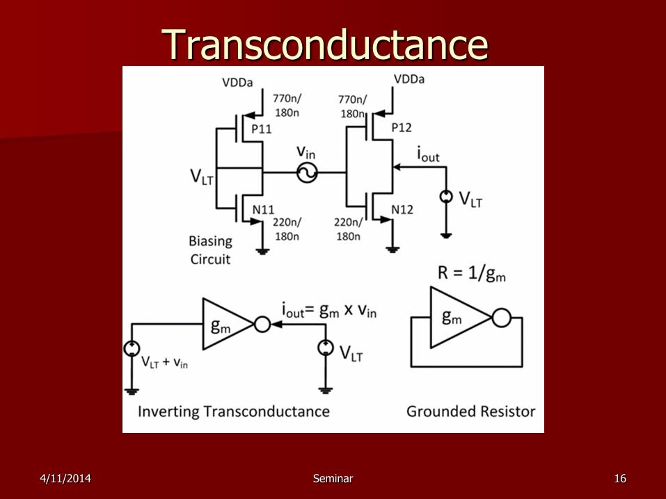
Transconductance
4/11/2014 Seminar 16
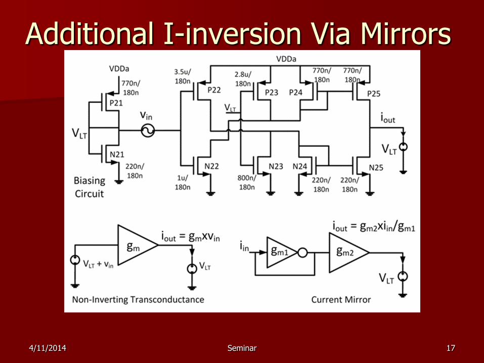
Additional I-inversion Via Mirrors
4/11/2014 Seminar 17

Both types of gm elements
4/11/2014 Seminar 18
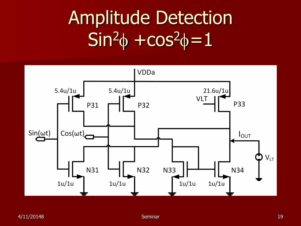
Amplitude Detection Sin2f +cos2f=1
4/11/20148 Seminar 19

Diode-Connected Squarer Gives Squareroot
4/11/2014 Seminar 20
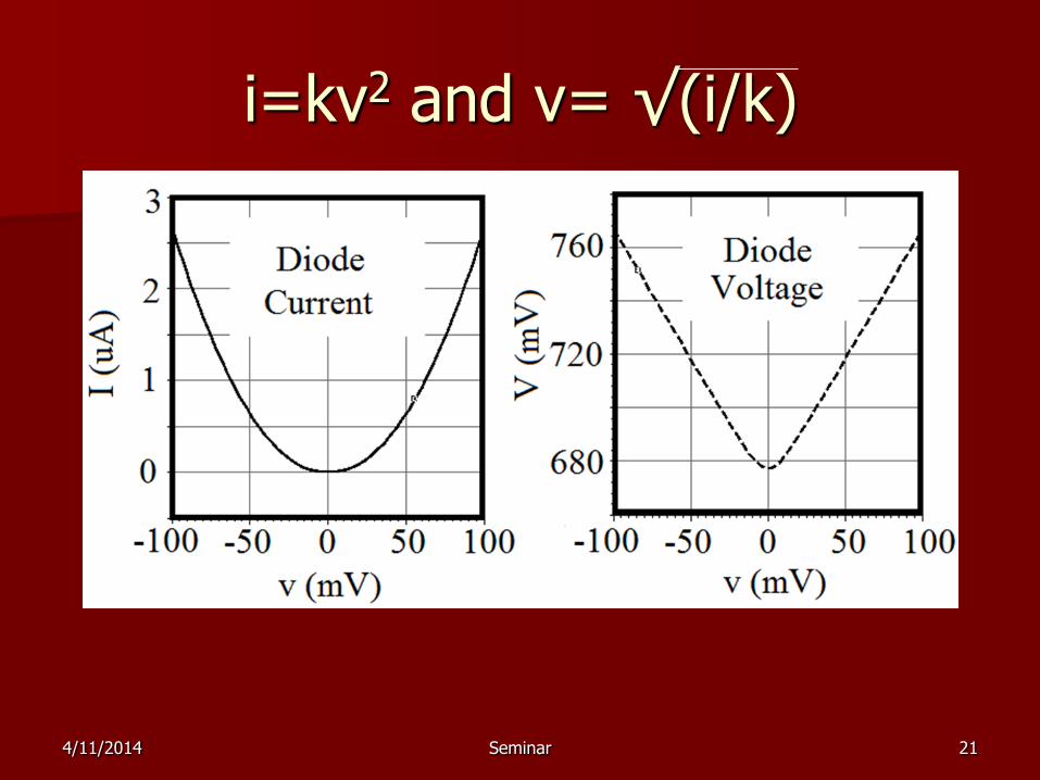
i=kv2 and v= √(i/k)
4/11/2014 Seminar 21

Sine and Cosine Outputs
4/11/2014 Seminar 22
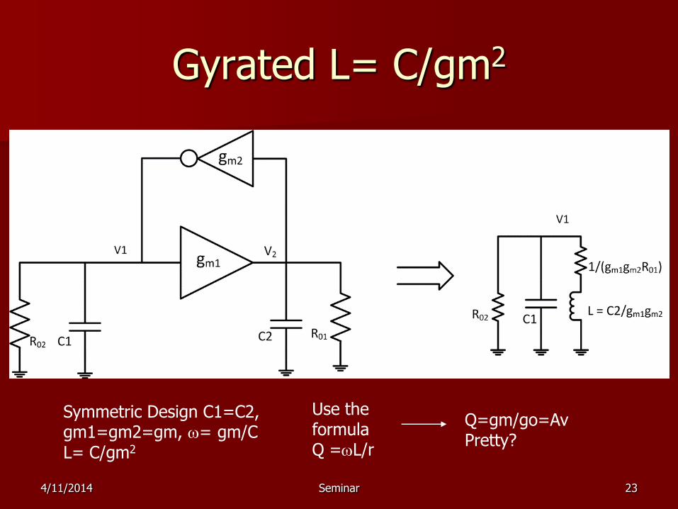
Gyrated L= C/gm2
4/11/2014 Seminar 23
Use the formula Q =wL/r
Symmetric Design C1=C2, gm1=gm2=gm, w= gm/C L= C/gm2
Q=gm/go=Av Pretty?
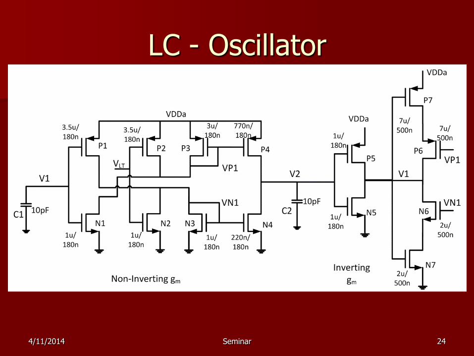
LC - Oscillator
4/11/2014 Seminar 24
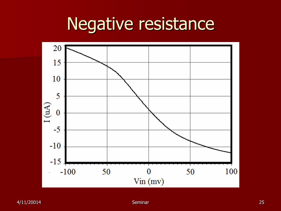
Negative resistance
4/11/20014 Seminar 25

Cap-Scaling by shunt Ai NFB
4/11/2014 Seminar 26

Controlled Oscillators for Low-Power ADC
A controlled- Oscillator with linear tuning characteristics quantizes phase which is proportional to the integral of the input. A key objective is to design an ICO with adequate linearity.( Peijun Wang)
Count the output frequency for a known period : Too slow
Both the operations of integration and quantization are performed by a simple controlled oscillator. In a traditional S-D converter we do this with an op-amp integrator and 1-b comparator
Low-power converters are needed for v/i- meters, Bio, Audio signals
In two-step converters the residue from the first step is converted with a VCO or Voltage to time converter.
4/11/2014 Seminar 27

ICO integrates and quantizes
4/11/2014 Seminar 28
Think that the Integrator with a rest switch to short C when VC reaches VREF (2p)
Counter quantizes Phase at 2p IIN
f 2p
When we want to integrate for a long time ( say one year) we abandon our inhibitions and jump into the digital world for obvious reasons. Living beings have built-in clocks (obviously not designed in Si Labs). Recently I found out that that the DNA is piezo-electric! Why do we integrate for a long time? ( think of 401K or 401 M). Generate gain (money grows without paying tax). Now we differentiate in the digital domain to get the signal and in that process shape the additive quantization noise.
+VC- VREF

Source-Coupled Multivibrator
4/11/2014 Seminar 29
(IIN/C)(T/2) = 2 IIN R
Rr Rr I cancels and f ∞ CR
(I/C)(T/2) = 2 l-1
We get linear current- control of Frequency
First Consider Resistive Loads
Substitute Active loads
11
1 1 1
2 1 2
Simple circuit Works at High frequencies 6-bit INL is obtainable Without calibration
There are many ways to clamp The voltage change across the load
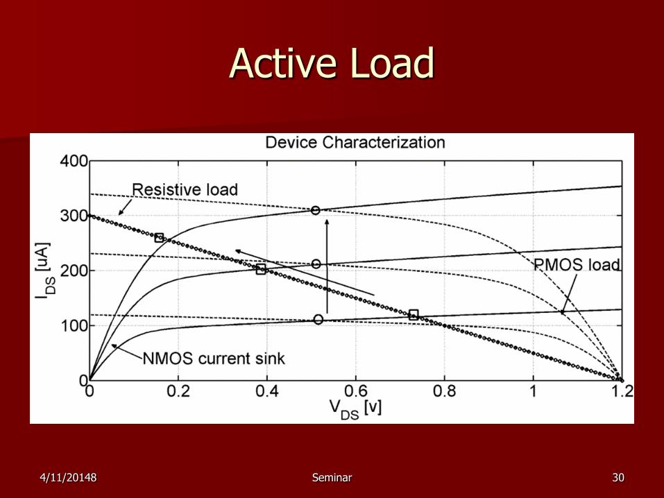
Active Load
4/11/20148 Seminar 30
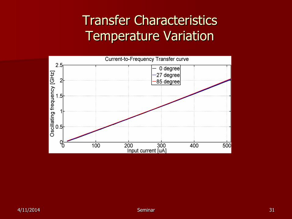
Transfer Characteristics Temperature Variation
4/11/2014 Seminar 31
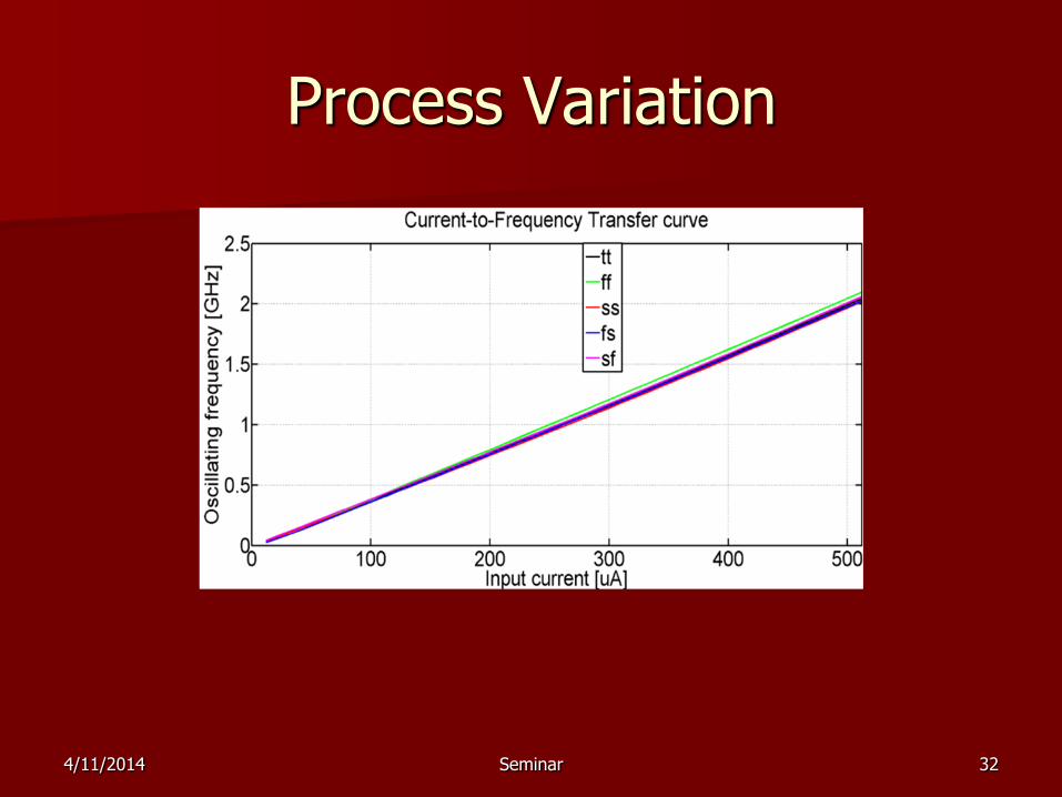
Process Variation
4/11/2014 Seminar 32
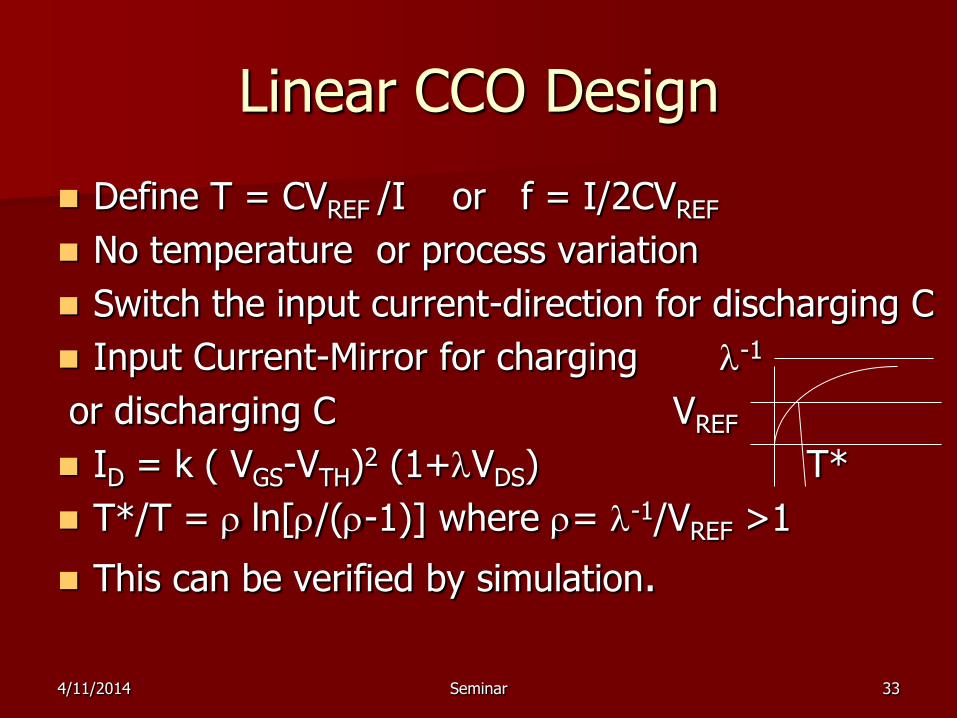
Linear CCO Design
Define T = CVREF /I or f = I/2CVREF
No temperature or process variation
Switch the input current-direction for discharging C
Input Current-Mirror for charging l-1
or discharging C VREF
ID = k ( VGS-VTH)2 (1+lVDS) T*
T*/T = r ln[r/(r-1)] where r= l-1/VREF >1
This can be verified by simulation.
4/11/2014 Seminar 33

Switching Delay
4/11/2014 Seminar 34

Model
f = 1/ (T + 2td)
td= c’/g = c’/ √(kIIN)
DV= (IIN/C) td = (IIN/C) [c’/ √(kIIN)]
DV=aVON where VON =√(IIN/k) and a= c’/C
DV is an offset in a differential pair or the VDS of a triode-operated output transistor of a current-mirror.
4/11/2014 Seminar 35
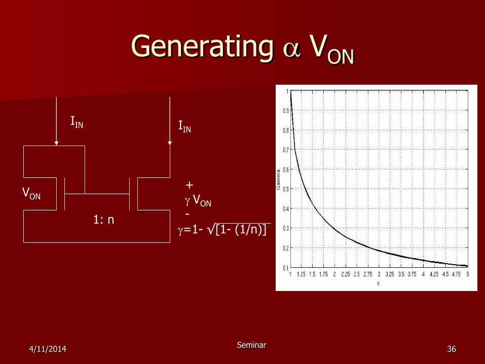
Generating a VON
4/11/2014 Seminar
36
VON
1: n
IIN IIN
+ g VON -
g=1- √[1- (1/n)]
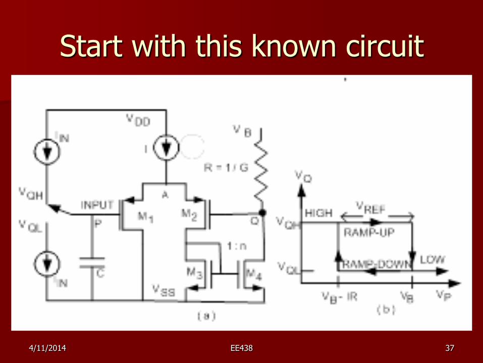
Start with this known circuit
4/11/2014 EE438 37
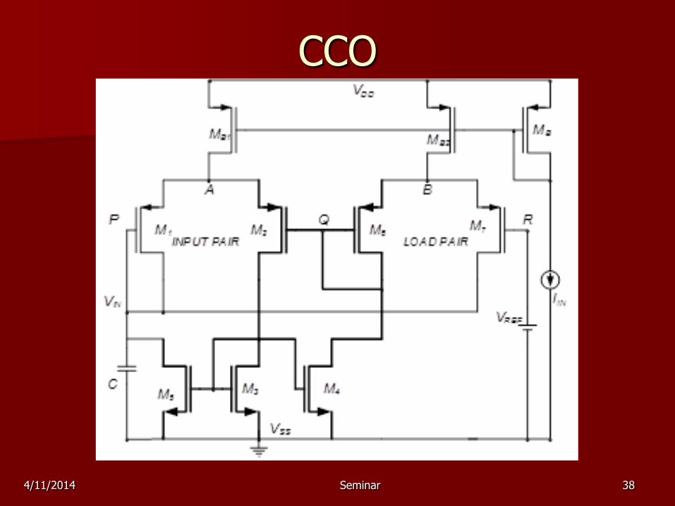
CCO
4/11/2014 Seminar 38
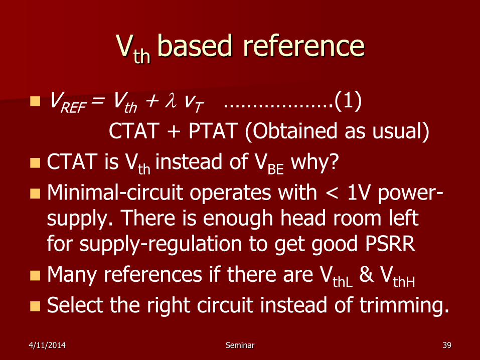
Vth based reference
VREF = Vth + l vT ……………….(1)
CTAT + PTAT (Obtained as usual)
CTAT is Vth instead of VBE why?
Minimal-circuit operates with < 1V power-supply. There is enough head room left for supply-regulation to get good PSRR
Many references if there are VthL & VthH
Select the right circuit instead of trimming.
4/11/2014 Seminar 39
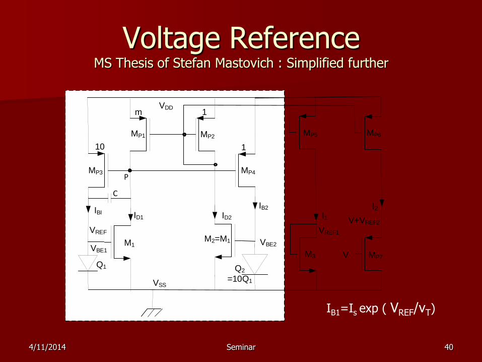
Voltage Reference MS Thesis of Stefan Mastovich : Simplified further
4/11/2014 Seminar 40
Q2
=10Q1
M2=M1
MP2
VDD
VSS
IB2
1
ID2
VBE2
I1
I2
MP4
1
V
V+VREF2
VREF1
MP5 MP6
M3 MP7
Q1
M1
MP1
10
IBI ID1
m
VBE1
MP3
VREF
P
C
IB1=Is exp ( VREF/vT)

How it works
+ FB for CM from VBE1 = –FB, from VBE2 for m>1
The currents balance at the node P giving
k (VBE1-Vth)2 = m k(VBE2-Vth)
2
VBE1-Vth = √m (VBE2-Vth)
VBE1- VBE2 = (VBE2 - Vth) (√m -1)
(gVPTAT)/(√m -1) +Vth = VBE2
VBE1= (gVPTAT) (√m) /(√m -1)
4/11/2014 Seminar 41

4/11/2014 seminar
42
m
(√m) /(√m -1)
PTAT Gain
Know more about signals
Signals vary in time in different ways.
When we sample and hold we collect only the instantaneous value.
We throw away its history
Know its history and use it to estimate where it is heading.
Controlled oversampling enables this.
New ADC designs use all the information in novel ways to reduce power.
4/11/2014 Seminar 43
SAR using VCO
A comparator performs some amplification a single-bit quantization.
– It has an amplifier and a latch
– What kind of an amplifier is it? Is it really algebraic? At high speeds it is more like a gm/c pseudo integrator
– What does a latch do? Vo e t/t
CCO Integrates and does multi-bit quantization.
4/11/2014 Seminar 44
Getting More Information to Simplify Search
Oversample with delayed clocks
This is not a clock- multiplexed ADC
Delay need not be exact fraction of Tclk
We estimate derivatives
This information is used to simplify the search
Can we reduce N to N/2 to obtain N-bits?
4/11/2014 Seminar 45