Embed Size (px)
Citation preview

ANALOG-BASEBAND ARCHITECTURES AND CIRCUITS FOR MULTISTANDARD AND LOW-VOLTAGE WIRELESS TRANSCEIVERS

ANALOG CIRCUITS AND SIGNAL PROCESSING SERIES
Consulting Editor: Mohammed Ismail. Ohio State University Titles in Series:
Pui-In Mak, Seng-Pan U, Rui Paulo Martins ISBN: 978-1-4020-6432-6
ULTRA LOW POWER CAPACITIVE SENSOR INTERFACES Bracke, W., Puers, R. (et al.)
BROADBAND OPTO-ELECTRICAL RECEIVERS IN STANDARD CMOS Hermans, C., Steyaert, M.
CMOS MULTI-CHANNEL SINGLE-CHIP RECEIVERS FOR MULTI-GIGABIT OPT… Muller, P., Leblebici, Y.
SWITCHED-CAPACITOR TECHNIQUES FOR HIGH-ACCURACY FILTER AND ADC… Quinn, P.J., Roermund, A.H.M.v.
LOW-FREQUENCY NOISE IN ADVANCED MOS DEVICES von Haartman, M., Östling, M.
Bourdi, Taoufik, Kale, Izzet
ANALOG CIRCUIT DESIGN TECHNIQUES AT 0.5V Chatterjee, S., Kinget, P., Tsividis, Y., Pun, K.P. ISBN-10: 0-387-69953-8
IQ CALIBRATION TECHNIQUES FOR CMOS RADIO TRANCEIVERS Chen, Sao-Jie, Hsieh, Yong-Hsiang ISBN-10: 1-4020-5082-8
FULL-CHIP NANOMETER ROUTING TECHNIQUES Ho, Tsung-Yi, Chang, Yao-Wen, Chen, Sao-Jie ISBN: 978-1-4020-6194-3
THE GM/ID DESIGN METHODOLOGY FOR CMOS ANALOG LOW POWER INTEGRATED CIRCUITS Jespers, Paul G.A. ISBN-10: 0-387-47100-6
PRECISION TEMPERATURE SENSORS IN CMOS TECHNOLOGY Pertijs, Michiel A.P., Huijsing, Johan H. ISBN-10: 1-4020-5257-X
CMOS CURRENT-MODE CIRCUITS FOR DATA COMMUNICATIONS Yuan, Fei ISBN: 0-387-29758-8
RF POWER AMPLIFIERS FOR MOBILE COMMUNICATIONS Reynaert, Patrick, Steyaert, Michiel ISBN: 1-4020-5116-6
Rudiakova, A.N., Krizhanovski, V.
CMOS CASCADE SIGMA-DELTA MODULATORS FOR SENSORS AND TELECOM del Río, R., Medeiro, F., Pérez-Verdú, B., de la Rosa, J.M., Rodríguez-Vázquez, A.
SIGMA DELTA A/D CONVERSION FOR SIGNAL CONDITIONING Philips, K., van Roermund, A.H.M.
CALIBRATION TECHNIQUES IN NYQUIST A/D CONVERTERS van der Ploeg, H., Nauta, B.
ADAPTIVE TECHNIQUES FOR MIXED SIGNAL SYSTEM ON CHIP Fayed, A., Ismail, M.
WIDE-BANDWIDTH HIGH-DYNAMIC RANGE D/A CONVERTERS Doris, Konstantinos, van Roermund, Arthur, Leenaerts, Domine
Pastre, Marc, Kayal, Maher Vol. 870, ISBN: 1-4020-4252-3
HIGH-SPEED PHOTODIODES IN STANDARD CMOS TECHNOLOGY Radovanovic, Sasa, Annema, Anne-Johan, Nauta, Bram Vol. 869, ISBN: 0-387-28591-1
ISBN: 978-1-4020-6231-5
ISBN: 978-1-4020-6221-6
ISBN: 978-1-4020-5911-7
ISBN: 978-1-4020-6257-5
ISBN: 978-1-4020-5909-4
ISBN: 978-1-4020-5927-8
ADVANCED DESIGN TECHNIQUES FOR RF POWER AMPLIFIERS
ISBN: 1-4020-4638-3
ISBN: 1-4020-4775-4
Vol. 874, ISBN: I-4020-4679-0
Vol. 873, ISBN: 1-4020-4634-0
Vol. 872, ISBN: 0-387-32154-3
Vol. 871, ISBN: 0-387-30415-0
WITH CASE STUDIES METHODOLOGY FOR THE DIGITAL CALIBRATION OF ANALOG CIRCUITS AND SYSTEMS:
MULTI-GIGAHERTZ APPLICATIONS CMOS SINGLE CHIP FAST FREQUENCY HOPPING SYNTHESIZERS FOR WIRELESS
LOW-VOLTAGE WIRELESS TRANSCEIVERS ANALOG-BASEBAND ARCHITECTURES AND CIRCUITS FOR MULTISTANDARD AND

ANALOG-BASEBAND ARCHITECTURES AND CIRCUITS FOR MULTISTANDARD AND LOW-VOLTAGE WIRELESS TRANSCEIVERS
Pui-In Mak
University of Macau, China
Seng-Pan U
University of Macau and Chipidea Microelectronics (Macau), Ltd., China
Rui Paulo Martins
University of Macau, China, and Technical University of Lisbon, Portugal

A C.I.P. Catalogue record for this book is available from the Library of Congress.
Published by Springer,
P.O. Box 17, 3300 AA Dordrecht, The Netherlands.
www.springer.com
Printed on acid-free paper
All Rights Reserved
No part of this work may be reproduced, stored in a retrieval system, or transmitted
in any form or by any means, electronic, mechanical, photocopying, microfilming, recording
or otherwise, without written permission from the Publisher, with the exception
of any material supplied specifically for the purpose of being entered
and executed on a computer system, for exclusive use by the purchaser of the work.
© 2007 Springer
ISBN 978-1-4020-6432-6 (HB)
ISBN 978-1-4020-6433-3 (e-book)

This book is dedicated to
Our Families

Contents
Dedication v
List of Abbreviations
1 INTRODUCTION 1 1. Evolution of wireless communications ............................................1 2. Wireless-IC design challenges and future prospects ........................2 3. Research objectives ..........................................................................4
3.1 Multistandard-compliant analog-baseband architectures .........4 3.2 Low-voltage analog-baseband functional blocks .....................5 3.3 A fully integrated multistandard-compliant low-voltage
analog-baseband platform for wideband applications ..............6 References ..............................................................................................6
2 TRANSCEIVER ARCHITECTURE SELECTION – REVIEW, STATE-OF-THE-ART SURVEY AND CASE STUDY 9
1. Introduction ......................................................................................9 2. Receiver (RX) architecture.............................................................10
2.1 Superheterodyne receiver .......................................................10 2.2 Image-rejection receiver – Hartley and Weaver.....................11 2.3 Zero-IF receiver......................................................................12 2.4 Low-IF receiver ......................................................................12
vii
Preface xi
Aknowledgments xv
xvii

viii Contents
2.5 Comparison of different receiver architectures ......................14 3. Transmitter (TX) architecture ........................................................14
3.1 Superheterodyne transmitter...................................................14 3.2 Direct-up transmitter ..............................................................15 3.3 Two-step-up transmitter .........................................................16 3.4 Comparison of different transmitter architectures..................17
4. RX and TX architectures for modern wireless communication systems ...........................................................................................17 4.1 GSM/DCS/PCS ......................................................................17 4.2 WCDMA (UMTS)..................................................................18 4.3 802.11x and HiperLAN 2 .......................................................19 4.4 Bluetooth (802.15.1), HomeRF, ZigBee (802.15.4)
and Ultra Wideband (802.15.3) ..............................................20 5. Survey of the state-of-the-art works for modern wireless
standards.........................................................................................21 6.
6.1 6.2 WPAN/WLAN transceivers for Bluetooth/802.11b...............25 6.3 WLAN transceivers for 802.11a/b/g ......................................28
7.
3 TWO-STEP CHANNEL SELECTION – A TECHNIQUE FOR
1. 2.
2.1 Conventional: fixed LORF
2.2 Conventional: varying LORF
2.3 Proposed two-step channel selection: coarse-varying LORF
3. 3.1 3.2 3.3 3.4 3.5
4. 5.
5.1 5.2
6.
Case study ......................................................................................23 Cellular receiver: GSM/DCS/PCS/WCDMA.........................23
Summary ........................................................................................31 References ............................................................................................32
MULTISTANDARD TRANSCEIVER FRONT-ENDS 41 Introduction ....................................................................................41 Conventional and proposed channel-selection schemes.................42
+ varying IF..................................42 + fixed IF..................................44
+ fine-varying IF ...........................................................44 Low-IF/zero-IF reconfigurable receiver design .............................49
System-design overview.........................................................49 Proposed receiver architecture................................................50 Step-1: RF AFE in low-IF mode ............................................52 Step-2: IF AFE in low-IF modes A and B..............................53Step-2: IF AFE in zero-IF mode.............................................54
Direct-up/two-step-up reconfigurable transmitter design...............55 Reconfigurable IF AFE design.......................................................56
Triple-mode channel-selection filter ......................................56 Multifunctional sampling-mixer scheme................................60
Summary ........................................................................................68 References ............................................................................................68

Contents ix
4 SYSTEM DESIGN OF A SIP RECEIVER FOR IEEE 802.11A/B/G
1. 2.
2.1 2.2 2.3 Proposed baseband-signal conditioning for cost-efficient
2.4 Proposed two-step channel-selection technique for radio
3. Translating the 802.11a, b and g standards to receiver design
4. 5. 6. 7.
5 1. 2. 3. 4. 5. 6. 7.
7.1 8.
8.1 8.2 Basic principle 2 – negative feedback for noise
8.3 8.4 Block-level design – convergent speed, stability
8.5 8.6
9. Series-switching mixer-quad, multi-phase I/Q generator
9.1 9.2 9.3 9.4
WLAN 71 Introduction ....................................................................................71 System design.................................................................................72
Proposed 3D stacked system partition for SiP integration .....72 Proposed flexible-IF reception for multistandardability.........75
reconfiguration .......................................................................76
front-end simplification ..........................................................78
specification ...................................................................................79 Gain plan ........................................................................................81 Specification of the analog baseband .............................................82 ADC requirement ...........................................................................84 Summary ........................................................................................85
References ............................................................................................86
LOW-VOLTAGE ANALOG-BASEBAND TECHNIQUES 89 Introduction ....................................................................................89 Operational amplifier (OpAmp) .....................................................90 CT level shifter...............................................................................91 Linear R-to-I converter...................................................................92 CT CMFB.......................................................................................93 Current switch ................................................................................94 MOS capacitor................................................................................95
Parallel-compensated depletion-mode MOS capacitor ..........96 Inside-OpAmp dc-offset canceler (DOC) ......................................99
Basic principle 1 – design for switchability ...........................99
and nonlinearity reduction ....................................................101 Basic principle 3 – negative feedback for area savings........101
and coverable range..............................................................103Transistor-level implementation...........................................105 Simulation results .................................................................107
and CSF (codesign) ......................................................................111 Basic principles of switching mixer .....................................111 Low-voltage switching mixer...............................................111 Low-voltage SS mixer-quad and I/Q generator....................113 Mismatch analysis ................................................................117

x Contents
9.5 9.6
10.1 Background – limitations of switched-resistor PGA
6 AN EXPERIMENTAL 1-V SIP RECEIVER ANALOG-BASEBAND
1. 2. 3. 4.
4.1 4.2 4.3
5. 6. 7.
7.1 7.2 7.3
8.
7 1. 2.
2.1 2.2
3.
Low-voltage CSF..................................................................118Design example and simulation results ................................119
10. SCR programmable-gain amplifier ..............................................120
in low-voltage operation.......................................................120 10.2 Operating principles .............................................................122 10.3 R-to-I conversion circuit.......................................................123 10.4 Feedback factor stabilization ................................................125 10.5 SCR PGA in 1-V and sub-1V operation...............................126 10.6 Linearity consideration.........................................................127 10.7 Noise consideration ..............................................................127 10.8 Design example ....................................................................129
11. Techniques reusability in advanced technology nodes.................137 12. Summary ......................................................................................139 References ..........................................................................................139
Introduction ..................................................................................143 Receiver architecture....................................................................143 Simulation methodology ..............................................................145 Circuit implementation.................................................................147
Preselect filter and DQDC and CLKGEN............................147 Channel-selection LPF, PGA and DOC scheme ..................148 Design of I/O circuitry..........................................................150
Simulation results .........................................................................151 Silicon implementation and test strategy......................................152 Experimental results .....................................................................156
SCR programmable-gain amplifier ......................................159 Analog-baseband IC .............................................................162
Summary ......................................................................................169 References ..........................................................................................169
CONCLUSIONS 171 Concluding remarks .....................................................................171 Benchmarks ..................................................................................173
Functional-block level ..........................................................173 Subsystem level ....................................................................174
Recommendations for future work...............................................175 References ..........................................................................................176
Double-quadrature-downconversion filter ...........................156
IC FOR IEEE 802.11A/B/G WLAN 143
Preface
The prospect of initializing a network-ubiquitous society in the years to come has led to the development of multistandard-compliant wireless transceivers for seamless roaming among multiple networks. To ensure a commercial success of such a development, the manufacturing cost and power consumption of the system chips have to be minimized. The use of an advanced technology and a high level of integration have continued to be the most effective ways for cost and power minimization, given that wireless chips integrate large amounts of digital logic for computation. Regrettably, entering into the nanoelectronics era, the thinner transistor gate oxide implicates great challenges in the design of the analog front-ends. While a low-voltage supply is imposed to maintain device reliability, a relatively large threshold voltage is also necessitated to limit the leakage current. Thus, transceiver architectures and circuits which will befit future full integration of multistandard wireless transceivers in sub-1V nanoscale CMOS processes must be highly reconfigurable and robustly operational underneath a low-voltage supply.
This book presents novel analog-baseband architectures and circuits that help realizing multistandard and low-voltage wireless transceivers. The main contents are presented from Chapter 2 to Chapter 6, as pictorially outlined in Figure 1.
Chapter 1 overviews the current wireless-IC developments and presents
the motivation and research objectives of this book.
xi

Figure 1. Outline of the book Chapter 2 studies the fundamental receiver and transmitter architectures
and reviews the physical layer (PHY) specifications of modern wireless
Preface xii

communication standards. A statistical summary (with 100+ references) of most exploitation transmitter, receiver and transceiver architectures for modern wireless communication systems has been surveyed. The references are collected from the solid-state circuit forums: ISSCC, CICC, VLSI and ESSCIRC, from 1997 to 2005. The final part presents case studies of the state-of-the-art multistandard receivers and trans-ceivers. Their achieved performances are compared in relation to their architectural choices and levels of block sharing.
Chapter 3 introduces a novel coarse-RF fine-IF (two-step) channel-
selection technique. Through the reconfiguration of receiver and trans-mitter analog basebands, it enables not only relaxation of the RF frequency synthesizer’s and local oscillator’s design specifications, but also an efficient multistandard compliance by synthesizing the low-IF/ zero-IF mode in the receiver; and the direct-up/two-step-up mode in the trans-mitter. The reconfiguration is mainly contributed by a triple-mode channel-select filter and a multifunctional sampling-mixer scheme.
Chapter 4 presents the system design of a system-in-a-package (SiP)
receiver analog baseband for IEEE 802.11a/b/g WLAN. It not only has the proposed two-step channel-selection technique reinforced, but also features globally a 3D-stack SiP floorplan for testability and routability, a flexible-IF (low-IF/zero-IF) reception capability and an area-efficient baseband-signal conditioning approach for different modes of operation.
Chapter 5 deals with the functional-block design of the above-men-
tioned receiver analog baseband with emphasis on reconfigurability, low-voltage supply, power and area savings. Methodical description of low-voltage circuit subblocks is given first, followed by the presentation of three novel functional blocks:
ing mixer-quad realizes a wideband mismatch-insensitive I/Q demo-dulation while offering the capabilities of clock-rate-defined IF reception, channel-selection filtering and sideband selection.
2. A switched-current-resistor programmable-gain amplifier provides a transient-free constant-bandwidth gain adjustment.
Preface
xiii
1. A double-quadrature-downconversion filter based on a series-switch-

3. An inside-OpAmp dc-offset canceler saves the silicon area required for realizing a large time constant on chip while maximizing its highpass-pole switchability for fast settling in dc-offset transients.
Chapter 6 summarizes the design issues, test strategy and experimental
results of a low-voltage receiver analog-baseband IC for IEEE 802.11a/ b/g WLAN. It is based on the system described in Chapter 4 and the low-voltage functional blocks presented in Chapter 5. A special test strategy enabled precision building-block and full subsystem characterization is also proposed.
Chapter 7 draws the relevant concluding remarks and benchmarks the
position of the described works to the state of the art. Timely future deve-lopments extending the current research are also suggested.
Pui-In Mak Seng-Pan U
Rui Paulo Martins
Preface xiv

Aknowledgments
We would like to thank Professor Kenneth W. Martin (University of Toronto), Professor Peter Chung-Yu Wu (National Chiao-Tung University), Professor Zhihua Wang (Tsinghua University), Professor Vai-Pan Iu (University of Macau) and Professor Ying-Duo Han (University of Macau) for examining the Ph.D. thesis of Pui-In Mak that is the basis of this book.
We acknowledge the Research Committee of University of Macau for the financial support, and the Macau Science and Technology Development Fund for funding a US patent application of this research.
We are very grateful to our colleagues, especially Ka-Hou Ao Ieong, in the Analog and Mixed-Signal VLSI Laboratory for fruitful discussions.
Finally, we send our heartfelt appreciation to our families, who endured our dedication to this book.
xv

List of Abbreviations
ΣΔ : Sigma-Delta 1/f : Flicker Noise 2SU : Two Step Up 3D : 3-Dimensional 3G/4G : 3rd/4th Generation A-BS : Analog-Baseband Sampling AC : Alternating Current ACPR : Adjacent Channel Power Ratio ADC (A/D) : Analog-to-Digital Converter A-DQS : Analog Double-Quadrature Sampling AFE : Analog Front-End AMPS : Advanced Mobile Phone System ANT : Antenna AWGN : Additive white Gaussian noise BB : Baseband BiCMOS : Bipolar Complementary Metal Oxide Semiconductor BPF : Bandpass Filter BSF : Band-Selection Filter BUF : Buffer BW : Bandwidth CCK : Complementary Code Keying CDMA : Code Division Multiple Access CF : Complex Filter
xvii

CICC : Custom Integrated Circuits Conference CG : Conversion Gain CLKGEN : Clock Generator CM : Common Mode CMFB : Common Mode Feedback CMOS : Complementary Metal Oxide Semiconductor CMRR : Common-Mode Rejection Ratio CQFP : Ceramic Quad Flat-Pack CS : Channel Spacing CSF : Channel-Selection Filter CSSF : Complex-Signal Spectral-Flow CT : Continuous-Time CV : Capacitance-Voltage DAC (D/A) : Digital-to-Analog Converter DC : Direct Current DCS : Digital Cellular System D-DQS : Digital Double-Quadrature Sampling DECT : Digital Enhanced Cordless Telecommunications DOC : DC-Offset Canceler DQDC : Double-Quadrature Downconverter DQDF : Double-Quadrature-Downconversion Filter DRC : Design Rule Check DSP : Digital Signal Processor DSSS : Direct-Sequence Spread Spectrum DU : Direct Up EDA : Electronics Design Automation EDGE : Enhanced Data rate for GSM Evolution EMI : Electromagnetic Interference ENOB : Effective Number of Bits ESD : Electrostatic Discharge ESSCIRC : European Solid-State Circuits Conference EVM : Error Vector Magnitude FET : Field Effect Transistor FFT : Fast Fourier Transform FHSS : Frequency-Hopping Spread Spectrum FS : Frequency Synthesizer
List of Abbreviationsxviii

GBW : Gain-Bandwidth Product GCA : Gain-Controllable Amplifier GPS : Global-Positioning System GSM : Global System for Mobile Communications HPF : Highpass Filter HD2/HD3 : Second-/Third-order Harmonic Distortion HIF : High Intermediate Frequency I : In Phase IC : Integrated Circuit I-CMFB : Input Common-Mode Feedback IEEE : Institute of Electrical and Electronics Engineering IF : Intermediate Frequency I/P : Input IM3 : Third-order Intermodulation Distortion IP3 : Third-order Intercept Point IRR : Image-Rejection Ratio ISM : Industrial, Scientific and Medical ISI : Intersymbol Interference ISSCC : International Solid-State Circuits Conference ITRS : International Technology Roadmap for Semiconductors I-to-V : Current-to-Voltage LC : Inductor-Capacitor LDO : Low-Dropout LIF : Low IF LNA : Low-Noise Amplifier LO : Local Oscillator LPF : Lowpass Filter LV : Low Voltage LVS : Layout versus Schematic MAC : Medium Access Control MEMS : Micro-Electro-Mechanical Systems MIMO : Multiple-Input Multiple-Output MIX : Mixer MOSFET : Metal-Oxide Semiconductor Field-Effect Transistor NF : Noise Figure O-CMFB : Output Common-Mode Feedback
List of Abbreviations xix

OFDM : Orthogonal Frequency-Division Multiplexing O/P : Output OpAmp : Operational Amplifier OSR : Oversampling Ratio OTA : Operational Transconductance Amplifier PCB : Printed-Circuit Board PCS : Personal Communication System PER : Packet-Error Rate PGA : Programmable-Gain Amplifier PGC : Programmable-Gain Control PHY : Physical Layer PLL : Phase-Locked Loop PM : Phase Margin PN : Pseudorandom Noise PSD : Power Spectrum Density PSS : Power Supply Sensitivity PVT : Process, Voltage and Temperature Q : Quadrature Phase/Quality Factor QAM : Quadrature Amplitude Modulation QPSK : Quadrature Phase-Shift Keying QVCO : Quadrature Voltage Control Oscillator RC : Resistor-Capacitor REF : Reference R-to-I : Resistor-to-Current RF : Radio Frequency RFID : Radio Frequency Identification RSSI : Receiver Signal Strength Indicator RX : Receiver SAW : Surface Acoustic Wave SC : Switched Capacitor SCR : Switched Current Resistor SFDR : Spurious-Free Dynamic Range S/H : Sample-and-Hold SiGe : Silicon Germanium SiP : System-in-Package SMD : Surface-Mount Device
List of Abbreviations xx

SNR : Signal-to-Noise Ratio SoC : System-on-Chip SS : Series Switching SU : Superheterodyne TDMA : Time Division Multiple Access THD : Total Harmonic Distortion TX : Transmitter TXR : Transceiver UWB : Ultra Wideband VCM : Common Mode Voltage VCO : Voltage Controlled Oscillator VGA : Variable-Gain Amplifier VLSI : Symposium on VLSI Circuits V-to-I : Voltage-to-Current WCDMA : Wideband Code Division Multiple Access WLAN : Wireless Local Area Network WPAN : Wireless Body Area Network ZIF : Zero IF
List of Abbreviations xxi
Chapter 1
INTRODUCTION
1. EVOLUTION OF WIRELESS COMMUNICATIONS
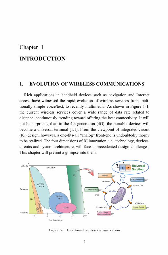
Rich applications in handheld devices such as navigation and Internet access have witnessed the rapid evolution of wireless services from tradi-tionally simple voice/text, to recently multimedia. As shown in Figure 1-1, the current wireless services cover a wide range of data rate related to distance, continuously trending toward offering the best connectivity. It will not be surprising that, in the 4th generation (4G), the portable devices will become a universal terminal [1.1]. From the viewpoint of integrated-circuit (IC) design, however, a one-fits-all “analog” front-end is undoubtedly thorny to be realized. The four dimensions of IC innovation, i.e., technology, devices, circuits and system architecture, will face unprecedented design challenges. This chapter will present a glimpse into them.
Figure 1-1. Evolution of wireless communications
1