Embed Size (px)
Citation preview

Analog and Digital Electronics
Daniel Adam Steck
Department of Physics, University of Oregon

Analog and Digital Electronics
Daniel Adam Steck
Department of Physics, University of Oregon

Copyright © 2015, by Daniel Adam Steck. All rights reserved.
This material may be distributed only subject to the terms and conditions set forth in the Open PublicationLicense, v1.0 or later (the latest version is available at http://www.opencontent.org/openpub/). Distri-bution of substantively modified versions of this document is prohibited without the explicit permission ofthe copyright holder. Distribution of the work or derivative of the work in any standard (paper) book formis prohibited unless prior permission is obtained from the copyright holder.
Original revision posted 28 January 2015.
This is revision 1.0.4, 1 August 2019.
Cite this document as:Daniel A. Steck, Analog and Digital Electronics, available online at http://steck.us/teaching (revision1.0.4, 1 August 2019).
Author contact information:Daniel SteckDepartment of Physics1274 University of OregonEugene, Oregon [email protected]

Acknowledgements
For comments and corrections, thanks to:
• Harrison Allen–Sutter (U. Oregon)
• Cameron Dennis (U. Oregon)
• Kyle Eichenberger (U. Oregon)
• Austin Ferrie (U. Oregon)
• Cody Jarrett (U. Oregon)
• Eric Torrence (U. Oregon)

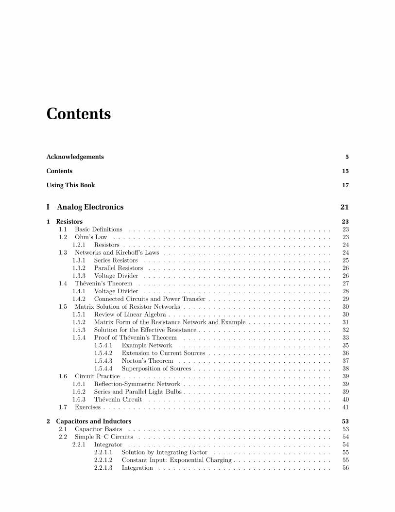
Contents
Acknowledgements 5
Contents 15
Using This Book 17
I Analog Electronics 21
1 Resistors 231.1 Basic Definitions . . . . . . . . . . . . . . . . . . . . . . . . . . . . . . . . . . . . . . . . . 231.2 Ohm’s Law . . . . . . . . . . . . . . . . . . . . . . . . . . . . . . . . . . . . . . . . . . . . 23
1.2.1 Resistors . . . . . . . . . . . . . . . . . . . . . . . . . . . . . . . . . . . . . . . . . . 241.3 Networks and Kirchoff’s Laws . . . . . . . . . . . . . . . . . . . . . . . . . . . . . . . . . . 24
1.3.1 Series Resistors . . . . . . . . . . . . . . . . . . . . . . . . . . . . . . . . . . . . . . 251.3.2 Parallel Resistors . . . . . . . . . . . . . . . . . . . . . . . . . . . . . . . . . . . . . 261.3.3 Voltage Divider . . . . . . . . . . . . . . . . . . . . . . . . . . . . . . . . . . . . . . 26
1.4 Thévenin’s Theorem . . . . . . . . . . . . . . . . . . . . . . . . . . . . . . . . . . . . . . . 271.4.1 Voltage Divider . . . . . . . . . . . . . . . . . . . . . . . . . . . . . . . . . . . . . . 281.4.2 Connected Circuits and Power Transfer . . . . . . . . . . . . . . . . . . . . . . . . . 29
1.5 Matrix Solution of Resistor Networks . . . . . . . . . . . . . . . . . . . . . . . . . . . . . . 301.5.1 Review of Linear Algebra . . . . . . . . . . . . . . . . . . . . . . . . . . . . . . . . . 301.5.2 Matrix Form of the Resistance Network and Example . . . . . . . . . . . . . . . . . 311.5.3 Solution for the Effective Resistance . . . . . . . . . . . . . . . . . . . . . . . . . . . 321.5.4 Proof of Thévenin’s Theorem . . . . . . . . . . . . . . . . . . . . . . . . . . . . . . 33
1.5.4.1 Example Network . . . . . . . . . . . . . . . . . . . . . . . . . . . . . . . 351.5.4.2 Extension to Current Sources . . . . . . . . . . . . . . . . . . . . . . . . . 361.5.4.3 Norton’s Theorem . . . . . . . . . . . . . . . . . . . . . . . . . . . . . . . 371.5.4.4 Superposition of Sources . . . . . . . . . . . . . . . . . . . . . . . . . . . . 38
1.6 Circuit Practice . . . . . . . . . . . . . . . . . . . . . . . . . . . . . . . . . . . . . . . . . . 391.6.1 Reflection-Symmetric Network . . . . . . . . . . . . . . . . . . . . . . . . . . . . . . 391.6.2 Series and Parallel Light Bulbs . . . . . . . . . . . . . . . . . . . . . . . . . . . . . . 391.6.3 Thévenin Circuit . . . . . . . . . . . . . . . . . . . . . . . . . . . . . . . . . . . . . 40
1.7 Exercises . . . . . . . . . . . . . . . . . . . . . . . . . . . . . . . . . . . . . . . . . . . . . . 41
2 Capacitors and Inductors 532.1 Capacitor Basics . . . . . . . . . . . . . . . . . . . . . . . . . . . . . . . . . . . . . . . . . 532.2 Simple R–C Circuits . . . . . . . . . . . . . . . . . . . . . . . . . . . . . . . . . . . . . . . 54
2.2.1 Integrator . . . . . . . . . . . . . . . . . . . . . . . . . . . . . . . . . . . . . . . . . 542.2.1.1 Solution by Integrating Factor . . . . . . . . . . . . . . . . . . . . . . . . 552.2.1.2 Constant Input: Exponential Charging . . . . . . . . . . . . . . . . . . . . 552.2.1.3 Integration . . . . . . . . . . . . . . . . . . . . . . . . . . . . . . . . . . . 56

8 Contents
2.2.2 Differentiator . . . . . . . . . . . . . . . . . . . . . . . . . . . . . . . . . . . . . . . 562.3 AC Signals and Complex Notation . . . . . . . . . . . . . . . . . . . . . . . . . . . . . . . 57
2.3.1 Complex Phase . . . . . . . . . . . . . . . . . . . . . . . . . . . . . . . . . . . . . . 572.3.2 Capacitive Reactance . . . . . . . . . . . . . . . . . . . . . . . . . . . . . . . . . . . 582.3.3 Inductive Reactance . . . . . . . . . . . . . . . . . . . . . . . . . . . . . . . . . . . . 592.3.4 Impedance . . . . . . . . . . . . . . . . . . . . . . . . . . . . . . . . . . . . . . . . . 592.3.5 Low-Pass Filter . . . . . . . . . . . . . . . . . . . . . . . . . . . . . . . . . . . . . . 592.3.6 Example Problem: Alternate Scaling . . . . . . . . . . . . . . . . . . . . . . . . . . 612.3.7 Example Problem: High-Pass Filter . . . . . . . . . . . . . . . . . . . . . . . . . . . 61
2.4 Phase . . . . . . . . . . . . . . . . . . . . . . . . . . . . . . . . . . . . . . . . . . . . . . . . 622.4.1 Example: Low-Pass Filter . . . . . . . . . . . . . . . . . . . . . . . . . . . . . . . . 63
2.5 Power . . . . . . . . . . . . . . . . . . . . . . . . . . . . . . . . . . . . . . . . . . . . . . . 642.6 Resonant Circuits . . . . . . . . . . . . . . . . . . . . . . . . . . . . . . . . . . . . . . . . . 65
2.6.1 Q Factor . . . . . . . . . . . . . . . . . . . . . . . . . . . . . . . . . . . . . . . . . . 662.6.1.1 Fundamental Definition . . . . . . . . . . . . . . . . . . . . . . . . . . . . 67
2.7 Coupled, Resonant Circuits . . . . . . . . . . . . . . . . . . . . . . . . . . . . . . . . . . . 682.8 Circuit Practice . . . . . . . . . . . . . . . . . . . . . . . . . . . . . . . . . . . . . . . . . . 72
2.8.1 Tesla Coil . . . . . . . . . . . . . . . . . . . . . . . . . . . . . . . . . . . . . . . . . 722.9 Exercises . . . . . . . . . . . . . . . . . . . . . . . . . . . . . . . . . . . . . . . . . . . . . . 73
3 Diodes 773.1 Ideal Diode . . . . . . . . . . . . . . . . . . . . . . . . . . . . . . . . . . . . . . . . . . . . 773.2 Vacuum Diodes . . . . . . . . . . . . . . . . . . . . . . . . . . . . . . . . . . . . . . . . . . 773.3 Semiconductor Diodes . . . . . . . . . . . . . . . . . . . . . . . . . . . . . . . . . . . . . . 783.4 Current–Voltage Characteristics . . . . . . . . . . . . . . . . . . . . . . . . . . . . . . . . . 80
3.4.1 Diode Law . . . . . . . . . . . . . . . . . . . . . . . . . . . . . . . . . . . . . . . . . 813.5 Zener Diodes . . . . . . . . . . . . . . . . . . . . . . . . . . . . . . . . . . . . . . . . . . . 823.6 Rectifier Circuits . . . . . . . . . . . . . . . . . . . . . . . . . . . . . . . . . . . . . . . . . 83
3.6.1 Half-Wave Rectifier . . . . . . . . . . . . . . . . . . . . . . . . . . . . . . . . . . . . 833.6.2 Full-Wave Rectifier . . . . . . . . . . . . . . . . . . . . . . . . . . . . . . . . . . . . 84
3.7 Schottky Diodes . . . . . . . . . . . . . . . . . . . . . . . . . . . . . . . . . . . . . . . . . . 853.8 Circuit Practice . . . . . . . . . . . . . . . . . . . . . . . . . . . . . . . . . . . . . . . . . . 86
3.8.1 Cockroft–Walton Multiplier . . . . . . . . . . . . . . . . . . . . . . . . . . . . . . . 863.9 Exercises . . . . . . . . . . . . . . . . . . . . . . . . . . . . . . . . . . . . . . . . . . . . . . 88
4 Bipolar Junction Transistors 914.1 Overview . . . . . . . . . . . . . . . . . . . . . . . . . . . . . . . . . . . . . . . . . . . . . . 914.2 Usage . . . . . . . . . . . . . . . . . . . . . . . . . . . . . . . . . . . . . . . . . . . . . . . . 924.3 Mechanism . . . . . . . . . . . . . . . . . . . . . . . . . . . . . . . . . . . . . . . . . . . . . 934.4 Packaging . . . . . . . . . . . . . . . . . . . . . . . . . . . . . . . . . . . . . . . . . . . . . 944.5 Transistor Switch . . . . . . . . . . . . . . . . . . . . . . . . . . . . . . . . . . . . . . . . . 95
4.5.1 Saturation Mode . . . . . . . . . . . . . . . . . . . . . . . . . . . . . . . . . . . . . 954.5.2 Forward-Active Mode . . . . . . . . . . . . . . . . . . . . . . . . . . . . . . . . . . . 964.5.3 Summary . . . . . . . . . . . . . . . . . . . . . . . . . . . . . . . . . . . . . . . . . . 96
4.6 Emitter Follower . . . . . . . . . . . . . . . . . . . . . . . . . . . . . . . . . . . . . . . . . 964.6.1 Input and Output Impedance . . . . . . . . . . . . . . . . . . . . . . . . . . . . . . 97
4.7 Transistor Current Source . . . . . . . . . . . . . . . . . . . . . . . . . . . . . . . . . . . . 994.7.1 Compliance . . . . . . . . . . . . . . . . . . . . . . . . . . . . . . . . . . . . . . . . 1004.7.2 Bias Network . . . . . . . . . . . . . . . . . . . . . . . . . . . . . . . . . . . . . . . 100
4.8 Common-Emitter Amplifier . . . . . . . . . . . . . . . . . . . . . . . . . . . . . . . . . . . 1024.9 Bias Network (AC Coupling) . . . . . . . . . . . . . . . . . . . . . . . . . . . . . . . . . . 1034.10 Transistor Differential Amplifier . . . . . . . . . . . . . . . . . . . . . . . . . . . . . . . . . 104
4.10.1 Differential-Only Input . . . . . . . . . . . . . . . . . . . . . . . . . . . . . . . . . . 106
Contents 9
4.10.2 Common-Mode-Only Input . . . . . . . . . . . . . . . . . . . . . . . . . . . . . . . . 1064.10.3 General Input and Common-Mode Rejection . . . . . . . . . . . . . . . . . . . . . . 1074.10.4 Improving the Differential Amplifier . . . . . . . . . . . . . . . . . . . . . . . . . . . 107
4.11 Ebers–Moll Model . . . . . . . . . . . . . . . . . . . . . . . . . . . . . . . . . . . . . . . . . 1084.11.1 Magnitudes . . . . . . . . . . . . . . . . . . . . . . . . . . . . . . . . . . . . . . . . 1094.11.2 Relation to β . . . . . . . . . . . . . . . . . . . . . . . . . . . . . . . . . . . . . . . 1094.11.3 Intrinsic Emitter Resistance . . . . . . . . . . . . . . . . . . . . . . . . . . . . . . . 1104.11.4 Current Mirror . . . . . . . . . . . . . . . . . . . . . . . . . . . . . . . . . . . . . . 110
4.11.4.1 Application to the Differential Amplifier . . . . . . . . . . . . . . . . . . . 1114.11.5 Other Refinements to the Transistor Model . . . . . . . . . . . . . . . . . . . . . . . 112
4.11.5.1 Temperature Dependence of the Base–Emitter Voltage . . . . . . . . . . . 1124.11.5.2 Early Effect . . . . . . . . . . . . . . . . . . . . . . . . . . . . . . . . . . . 1134.11.5.3 Miller Effect . . . . . . . . . . . . . . . . . . . . . . . . . . . . . . . . . . 1134.11.5.4 Variation of β . . . . . . . . . . . . . . . . . . . . . . . . . . . . . . . . . 114
4.12 Common-Emitter Amplifier Revisited: Emitter Degeneration . . . . . . . . . . . . . . . . 1144.13 Biasing the Push–Pull Pair . . . . . . . . . . . . . . . . . . . . . . . . . . . . . . . . . . . . 1164.14 Mathematical Modeling of DC BJT Behavior . . . . . . . . . . . . . . . . . . . . . . . . . 119
4.14.1 Ebers–Moll Model . . . . . . . . . . . . . . . . . . . . . . . . . . . . . . . . . . . . . 1194.14.2 Ebers–Moll–Early Model . . . . . . . . . . . . . . . . . . . . . . . . . . . . . . . . . 1214.14.3 Gummel–Poon Model . . . . . . . . . . . . . . . . . . . . . . . . . . . . . . . . . . . 121
4.15 Little-“h” Notation . . . . . . . . . . . . . . . . . . . . . . . . . . . . . . . . . . . . . . . . 1234.16 Circuit Practice . . . . . . . . . . . . . . . . . . . . . . . . . . . . . . . . . . . . . . . . . . 124
4.16.1 Transistor Switching an Inductive Load . . . . . . . . . . . . . . . . . . . . . . . . . 1244.16.2 Joule Thief . . . . . . . . . . . . . . . . . . . . . . . . . . . . . . . . . . . . . . . . . 1254.16.3 Solid-State Tesla Coil . . . . . . . . . . . . . . . . . . . . . . . . . . . . . . . . . . . 1264.16.4 Eric Clapton Signature Stratocaster Preamplifier . . . . . . . . . . . . . . . . . . . 1274.16.5 Op-Amp Internals . . . . . . . . . . . . . . . . . . . . . . . . . . . . . . . . . . . . . 127
4.17 Exercises . . . . . . . . . . . . . . . . . . . . . . . . . . . . . . . . . . . . . . . . . . . . . . 130
5 Field-Effect Transistors and Semiconductor Switching Devices 1395.1 JFET (Depletion-Mode FET) . . . . . . . . . . . . . . . . . . . . . . . . . . . . . . . . . . 1395.2 MOSFET (Enhancement-Mode FET) . . . . . . . . . . . . . . . . . . . . . . . . . . . . . . 1415.3 Quantitative FET Behavior . . . . . . . . . . . . . . . . . . . . . . . . . . . . . . . . . . . 142
5.3.1 Visualization . . . . . . . . . . . . . . . . . . . . . . . . . . . . . . . . . . . . . . . . 1435.4 Basic FET Circuits . . . . . . . . . . . . . . . . . . . . . . . . . . . . . . . . . . . . . . . . 146
5.4.1 JFET Current Source . . . . . . . . . . . . . . . . . . . . . . . . . . . . . . . . . . . 1465.4.2 JFET Source Follower . . . . . . . . . . . . . . . . . . . . . . . . . . . . . . . . . . 1465.4.3 JFET Common-Source Amplifier . . . . . . . . . . . . . . . . . . . . . . . . . . . . 1475.4.4 JFET Differential Amplifier . . . . . . . . . . . . . . . . . . . . . . . . . . . . . . . 1495.4.5 MOSFET Analog Switch . . . . . . . . . . . . . . . . . . . . . . . . . . . . . . . . . 150
5.5 Thyristors . . . . . . . . . . . . . . . . . . . . . . . . . . . . . . . . . . . . . . . . . . . . . 1515.5.1 SCRs . . . . . . . . . . . . . . . . . . . . . . . . . . . . . . . . . . . . . . . . . . . . 151
5.5.1.1 Example: Latching Switch with Power-Supply Fault Protection . . . . . . 1535.5.2 DIACs and TRIACs . . . . . . . . . . . . . . . . . . . . . . . . . . . . . . . . . . . . 153
5.5.2.1 Light Dimmer . . . . . . . . . . . . . . . . . . . . . . . . . . . . . . . . . 1545.6 IGBTs: Switching Very Large Voltages and Currents . . . . . . . . . . . . . . . . . . . . . 155
5.6.1 Driver Circuitry . . . . . . . . . . . . . . . . . . . . . . . . . . . . . . . . . . . . . . 1575.6.2 Inverter Circuits . . . . . . . . . . . . . . . . . . . . . . . . . . . . . . . . . . . . . . 158
5.6.2.1 Inverter-Based Tesla Coil . . . . . . . . . . . . . . . . . . . . . . . . . . . 1605.7 Circuit Practice . . . . . . . . . . . . . . . . . . . . . . . . . . . . . . . . . . . . . . . . . . 162
5.7.1 Touch Switch . . . . . . . . . . . . . . . . . . . . . . . . . . . . . . . . . . . . . . . 1625.7.2 JFET Op-Amp Internals . . . . . . . . . . . . . . . . . . . . . . . . . . . . . . . . . 163
5.8 Exercises . . . . . . . . . . . . . . . . . . . . . . . . . . . . . . . . . . . . . . . . . . . . . . 165
10 Contents
6 Vacuum Tubes 1676.1 Vacuum Diodes . . . . . . . . . . . . . . . . . . . . . . . . . . . . . . . . . . . . . . . . . . 167
6.1.1 Child–Langmuir Law . . . . . . . . . . . . . . . . . . . . . . . . . . . . . . . . . . . 1686.1.2 Vacuum Full-Wave Rectifier . . . . . . . . . . . . . . . . . . . . . . . . . . . . . . . 168
6.2 Vacuum Triodes . . . . . . . . . . . . . . . . . . . . . . . . . . . . . . . . . . . . . . . . . . 1696.2.1 Triode Voltage Ampifier (Common-Cathode Amplifier) . . . . . . . . . . . . . . . . 170
6.2.1.1 DC Bias . . . . . . . . . . . . . . . . . . . . . . . . . . . . . . . . . . . . . 1716.2.1.2 Naïve AC Analysis . . . . . . . . . . . . . . . . . . . . . . . . . . . . . . . 1726.2.1.3 Proper AC Analysis: Plate Resistance . . . . . . . . . . . . . . . . . . . . 173
6.2.2 Design Example: 12AX7 Preamplifier . . . . . . . . . . . . . . . . . . . . . . . . . . 1756.2.3 Phenomenological Triode Model . . . . . . . . . . . . . . . . . . . . . . . . . . . . . 175
6.3 Vacuum Tetrodes . . . . . . . . . . . . . . . . . . . . . . . . . . . . . . . . . . . . . . . . . 1776.4 Vacuum Pentodes and Beam Power Tubes . . . . . . . . . . . . . . . . . . . . . . . . . . . 178
6.4.1 Design Example: 6V6 Power Output Stage . . . . . . . . . . . . . . . . . . . . . . . 1806.4.2 Triode Connection . . . . . . . . . . . . . . . . . . . . . . . . . . . . . . . . . . . . . 183
6.5 Circuit Practice: Simple Tube Amplifier . . . . . . . . . . . . . . . . . . . . . . . . . . . . 1846.5.1 First Preamplifier Stage . . . . . . . . . . . . . . . . . . . . . . . . . . . . . . . . . 1856.5.2 Second Preamplifier Stage . . . . . . . . . . . . . . . . . . . . . . . . . . . . . . . . 1866.5.3 Power Amplifier Stage . . . . . . . . . . . . . . . . . . . . . . . . . . . . . . . . . . 1866.5.4 Feedback Loop . . . . . . . . . . . . . . . . . . . . . . . . . . . . . . . . . . . . . . . 1866.5.5 Power Supply . . . . . . . . . . . . . . . . . . . . . . . . . . . . . . . . . . . . . . . 187
7 Operational Amplifiers 1897.1 Op-Amp Basics . . . . . . . . . . . . . . . . . . . . . . . . . . . . . . . . . . . . . . . . . . 189
7.1.1 Usage: Open-Loop . . . . . . . . . . . . . . . . . . . . . . . . . . . . . . . . . . . . 1897.1.2 Usage: Closed-Loop . . . . . . . . . . . . . . . . . . . . . . . . . . . . . . . . . . . . 190
7.2 Op-Amp “Golden Rules” . . . . . . . . . . . . . . . . . . . . . . . . . . . . . . . . . . . . . 1907.3 Basic Op-Amp Circuits . . . . . . . . . . . . . . . . . . . . . . . . . . . . . . . . . . . . . . 190
7.3.1 Unity-Gain Buffer/Follower . . . . . . . . . . . . . . . . . . . . . . . . . . . . . . . 1907.3.2 Inverting Amplifier . . . . . . . . . . . . . . . . . . . . . . . . . . . . . . . . . . . . 191
7.3.2.1 Stability . . . . . . . . . . . . . . . . . . . . . . . . . . . . . . . . . . . . . 1927.3.3 Noninverting Amplifier . . . . . . . . . . . . . . . . . . . . . . . . . . . . . . . . . . 1937.3.4 Summing (Inverting) Amplifier . . . . . . . . . . . . . . . . . . . . . . . . . . . . . . 1937.3.5 Circuit Practice: Differential Amplifier . . . . . . . . . . . . . . . . . . . . . . . . . 194
7.4 Op-Amp Filters . . . . . . . . . . . . . . . . . . . . . . . . . . . . . . . . . . . . . . . . . . 1947.4.1 Op-Amp Differentiator . . . . . . . . . . . . . . . . . . . . . . . . . . . . . . . . . . 1957.4.2 Op-Amp Integrator . . . . . . . . . . . . . . . . . . . . . . . . . . . . . . . . . . . . 1957.4.3 Differentiator Issues . . . . . . . . . . . . . . . . . . . . . . . . . . . . . . . . . . . . 1967.4.4 Integrator Issues . . . . . . . . . . . . . . . . . . . . . . . . . . . . . . . . . . . . . . 1977.4.5 Sources of Integrator Error . . . . . . . . . . . . . . . . . . . . . . . . . . . . . . . . 198
7.4.5.1 Input Bias Current . . . . . . . . . . . . . . . . . . . . . . . . . . . . . . . 1987.4.5.2 Input Offset Voltage . . . . . . . . . . . . . . . . . . . . . . . . . . . . . . 200
7.4.6 Integrator Applications . . . . . . . . . . . . . . . . . . . . . . . . . . . . . . . . . . 2007.5 Instrumentation Amplifiers . . . . . . . . . . . . . . . . . . . . . . . . . . . . . . . . . . . . 201
7.5.1 “Classic” Instrumentation Amplifier . . . . . . . . . . . . . . . . . . . . . . . . . . . 2027.5.2 Instrumentation-Amplifier Applications . . . . . . . . . . . . . . . . . . . . . . . . . 203
7.5.2.1 Thermocouple Amplifier . . . . . . . . . . . . . . . . . . . . . . . . . . . . 2037.5.2.2 Differential Transmission for Noise Rejection . . . . . . . . . . . . . . . . 2047.5.2.3 AC-Coupled Inputs with High Impedance . . . . . . . . . . . . . . . . . . 205
7.6 Practical Considerations . . . . . . . . . . . . . . . . . . . . . . . . . . . . . . . . . . . . . 2067.6.1 Input-Bias Currents and Precision Amplifiers . . . . . . . . . . . . . . . . . . . . . 206
7.6.1.1 Inverting Amplifier . . . . . . . . . . . . . . . . . . . . . . . . . . . . . . . 2067.6.1.2 Balanced Input-Impedances: Inverting Amplifier . . . . . . . . . . . . . . 207

Contents 11
7.6.1.3 Balanced Input-Impedances: Noninverting Amplifier . . . . . . . . . . . . 2077.6.1.4 Input Offset Currents . . . . . . . . . . . . . . . . . . . . . . . . . . . . . 2087.6.1.5 Common-Mode Rejection Ratio . . . . . . . . . . . . . . . . . . . . . . . . 208
7.6.2 Power Supplies . . . . . . . . . . . . . . . . . . . . . . . . . . . . . . . . . . . . . . 2087.6.2.1 Power-Supply Rejection . . . . . . . . . . . . . . . . . . . . . . . . . . . . 2097.6.2.2 Power-Supply Bypass Capacitors . . . . . . . . . . . . . . . . . . . . . . . 209
7.7 Finite-Gain Analysis . . . . . . . . . . . . . . . . . . . . . . . . . . . . . . . . . . . . . . . 2117.7.1 Noninverting Amplifier . . . . . . . . . . . . . . . . . . . . . . . . . . . . . . . . . . 211
7.7.1.1 Gain Limits and Error . . . . . . . . . . . . . . . . . . . . . . . . . . . . . 2127.7.1.2 Insensitivity to Gain Variation . . . . . . . . . . . . . . . . . . . . . . . . 213
7.7.2 Feedback and Input Impedance . . . . . . . . . . . . . . . . . . . . . . . . . . . . . 2137.7.3 Feedback and Output Impedance . . . . . . . . . . . . . . . . . . . . . . . . . . . . 2147.7.4 Circuit Practice: Finite Gain in the Inverting Amplifier . . . . . . . . . . . . . . . . 215
7.8 Bandwidth . . . . . . . . . . . . . . . . . . . . . . . . . . . . . . . . . . . . . . . . . . . . . 2167.8.1 Slew Rate . . . . . . . . . . . . . . . . . . . . . . . . . . . . . . . . . . . . . . . . . 217
7.8.1.1 Slew Rate and Power-Boosted Op-Amps . . . . . . . . . . . . . . . . . . . 2177.8.2 Stability and Compensation . . . . . . . . . . . . . . . . . . . . . . . . . . . . . . . 219
7.8.2.1 Op-Amp Output and Capacitive Loads . . . . . . . . . . . . . . . . . . . 2207.9 Comparators . . . . . . . . . . . . . . . . . . . . . . . . . . . . . . . . . . . . . . . . . . . . 221
7.9.1 Schmitt Trigger . . . . . . . . . . . . . . . . . . . . . . . . . . . . . . . . . . . . . . 2227.10 Positive Feedback and Oscillator Circuits . . . . . . . . . . . . . . . . . . . . . . . . . . . . 223
7.10.1 Relaxation Oscillator . . . . . . . . . . . . . . . . . . . . . . . . . . . . . . . . . . . 2237.10.2 Buffered Phase-Shift Oscillator . . . . . . . . . . . . . . . . . . . . . . . . . . . . . . 224
7.11 Amplifier Noise Analysis . . . . . . . . . . . . . . . . . . . . . . . . . . . . . . . . . . . . . 2257.11.1 Sources of Noise . . . . . . . . . . . . . . . . . . . . . . . . . . . . . . . . . . . . . . 226
7.11.1.1 Johnson–Nyquist Noise . . . . . . . . . . . . . . . . . . . . . . . . . . . . 2267.11.1.2 “kT/C” Noise . . . . . . . . . . . . . . . . . . . . . . . . . . . . . . . . . . 2287.11.1.3 Shot Noise . . . . . . . . . . . . . . . . . . . . . . . . . . . . . . . . . . . 2287.11.1.4 1/f Noise . . . . . . . . . . . . . . . . . . . . . . . . . . . . . . . . . . . . 228
7.11.2 Estimation of Amplifier Noise . . . . . . . . . . . . . . . . . . . . . . . . . . . . . . 2297.11.2.1 Example: Precision Current Source . . . . . . . . . . . . . . . . . . . . . . 231
7.12 Circuit Practice . . . . . . . . . . . . . . . . . . . . . . . . . . . . . . . . . . . . . . . . . . 2357.12.1 Analog Computers . . . . . . . . . . . . . . . . . . . . . . . . . . . . . . . . . . . . 235
7.12.1.1 Proportional–Integral Amplifier . . . . . . . . . . . . . . . . . . . . . . . . 2357.12.1.2 Damped Harmonic Oscillator . . . . . . . . . . . . . . . . . . . . . . . . . 235
7.12.2 Gyrator . . . . . . . . . . . . . . . . . . . . . . . . . . . . . . . . . . . . . . . . . . . 2367.12.3 Guitar Preamp with Midrange Boost/Cut . . . . . . . . . . . . . . . . . . . . . . . 2387.12.4 Active Rectifiers . . . . . . . . . . . . . . . . . . . . . . . . . . . . . . . . . . . . . . 2417.12.5 Pulse-Area Stabilizer . . . . . . . . . . . . . . . . . . . . . . . . . . . . . . . . . . . 242
7.13 Exercises . . . . . . . . . . . . . . . . . . . . . . . . . . . . . . . . . . . . . . . . . . . . . . 244
8 PID Control 2618.1 Basics of Linear Control . . . . . . . . . . . . . . . . . . . . . . . . . . . . . . . . . . . . . 2618.2 Example: First-Order Plant, Proportional Control . . . . . . . . . . . . . . . . . . . . . . 262
8.2.1 General Result: Closed-Loop Transfer Function . . . . . . . . . . . . . . . . . . . . 2628.2.2 Frequency-Domain Solution . . . . . . . . . . . . . . . . . . . . . . . . . . . . . . . 2638.2.3 Time-Domain Solution . . . . . . . . . . . . . . . . . . . . . . . . . . . . . . . . . . 2638.2.4 Constant Input and Proportional Droop . . . . . . . . . . . . . . . . . . . . . . . . 263
8.3 Integral Control . . . . . . . . . . . . . . . . . . . . . . . . . . . . . . . . . . . . . . . . . . 2648.3.1 Example: First-Order Plant, Integral Control . . . . . . . . . . . . . . . . . . . . . 2648.3.2 Frequency Domain . . . . . . . . . . . . . . . . . . . . . . . . . . . . . . . . . . . . 264
8.4 Proportional–Integral (PI) Control . . . . . . . . . . . . . . . . . . . . . . . . . . . . . . . 2658.5 Proportional–Integral–Derivative (PID) Control . . . . . . . . . . . . . . . . . . . . . . . . 265
12 Contents
II Digital Electronics 267
9 Binary Logic and Logic Gates 2699.1 Binary Logic . . . . . . . . . . . . . . . . . . . . . . . . . . . . . . . . . . . . . . . . . . . . 2699.2 Binary Arithmetic . . . . . . . . . . . . . . . . . . . . . . . . . . . . . . . . . . . . . . . . 269
9.2.1 Unsigned Integers . . . . . . . . . . . . . . . . . . . . . . . . . . . . . . . . . . . . . 2699.2.1.1 Binary-Coded Decimal . . . . . . . . . . . . . . . . . . . . . . . . . . . . . 2709.2.1.2 Hexadecimal . . . . . . . . . . . . . . . . . . . . . . . . . . . . . . . . . . 270
9.2.2 Negative Values and Sign Conventions . . . . . . . . . . . . . . . . . . . . . . . . . 2709.2.2.1 Sign-Magnitude Convention . . . . . . . . . . . . . . . . . . . . . . . . . . 2709.2.2.2 Two’s Complement . . . . . . . . . . . . . . . . . . . . . . . . . . . . . . . 270
9.3 Logic Gates . . . . . . . . . . . . . . . . . . . . . . . . . . . . . . . . . . . . . . . . . . . . 2719.3.1 One-Input Gates . . . . . . . . . . . . . . . . . . . . . . . . . . . . . . . . . . . . . . 2719.3.2 Two-Input Gates . . . . . . . . . . . . . . . . . . . . . . . . . . . . . . . . . . . . . 272
9.3.2.1 AND and NAND . . . . . . . . . . . . . . . . . . . . . . . . . . . . . . . . 2729.3.2.2 OR and NOR . . . . . . . . . . . . . . . . . . . . . . . . . . . . . . . . . . 2729.3.2.3 Universal Gates . . . . . . . . . . . . . . . . . . . . . . . . . . . . . . . . . 2729.3.2.4 XOR and XNOR . . . . . . . . . . . . . . . . . . . . . . . . . . . . . . . . 272
9.3.3 More Complex Gates . . . . . . . . . . . . . . . . . . . . . . . . . . . . . . . . . . . 2739.4 Circuit Practice . . . . . . . . . . . . . . . . . . . . . . . . . . . . . . . . . . . . . . . . . . 2739.5 Exercises . . . . . . . . . . . . . . . . . . . . . . . . . . . . . . . . . . . . . . . . . . . . . . 274
10 Boolean Algebra 27710.1 Algebras and Boolean Algebra . . . . . . . . . . . . . . . . . . . . . . . . . . . . . . . . . . 27710.2 Boolean-Algebraic Theorems and Manipulations . . . . . . . . . . . . . . . . . . . . . . . . 278
10.2.1 De Morgan’s Theorems . . . . . . . . . . . . . . . . . . . . . . . . . . . . . . . . . . 27810.2.2 Absorption Theorems . . . . . . . . . . . . . . . . . . . . . . . . . . . . . . . . . . . 27810.2.3 Another Theorem . . . . . . . . . . . . . . . . . . . . . . . . . . . . . . . . . . . . . 27810.2.4 Example: XOR Gate . . . . . . . . . . . . . . . . . . . . . . . . . . . . . . . . . . . 278
10.2.4.1 NAND-Gate Realization . . . . . . . . . . . . . . . . . . . . . . . . . . . . 27910.2.5 Example: Algebraic Simplification . . . . . . . . . . . . . . . . . . . . . . . . . . . . 279
10.3 Karnaugh Maps . . . . . . . . . . . . . . . . . . . . . . . . . . . . . . . . . . . . . . . . . . 28010.3.1 Three-Input Example . . . . . . . . . . . . . . . . . . . . . . . . . . . . . . . . . . . 28010.3.2 Four-Input Example . . . . . . . . . . . . . . . . . . . . . . . . . . . . . . . . . . . . 28210.3.3 XOR Example . . . . . . . . . . . . . . . . . . . . . . . . . . . . . . . . . . . . . . . 28210.3.4 Race Hazards . . . . . . . . . . . . . . . . . . . . . . . . . . . . . . . . . . . . . . . 282
10.4 Circuit Practice . . . . . . . . . . . . . . . . . . . . . . . . . . . . . . . . . . . . . . . . . . 28410.4.1 Boolean-Algebra Theorems . . . . . . . . . . . . . . . . . . . . . . . . . . . . . . . . 28410.4.2 Karnaugh Map . . . . . . . . . . . . . . . . . . . . . . . . . . . . . . . . . . . . . . 284
10.5 Exercises . . . . . . . . . . . . . . . . . . . . . . . . . . . . . . . . . . . . . . . . . . . . . . 286
11 Physical Implementation of Logic Gates 29111.1 Simple Mechanical Switches . . . . . . . . . . . . . . . . . . . . . . . . . . . . . . . . . . . 29111.2 Diode Logic (DL) . . . . . . . . . . . . . . . . . . . . . . . . . . . . . . . . . . . . . . . . . 292
11.2.1 Diode Review . . . . . . . . . . . . . . . . . . . . . . . . . . . . . . . . . . . . . . . 29211.2.2 DL AND Gate . . . . . . . . . . . . . . . . . . . . . . . . . . . . . . . . . . . . . . . 29311.2.3 DL OR Gate . . . . . . . . . . . . . . . . . . . . . . . . . . . . . . . . . . . . . . . . 293
11.3 Resistor-Transistor Logic (RTL) . . . . . . . . . . . . . . . . . . . . . . . . . . . . . . . . . 29411.3.1 BJT Review . . . . . . . . . . . . . . . . . . . . . . . . . . . . . . . . . . . . . . . . 29411.3.2 RTL NOT Gate . . . . . . . . . . . . . . . . . . . . . . . . . . . . . . . . . . . . . . 29411.3.3 RTL NOR Gate . . . . . . . . . . . . . . . . . . . . . . . . . . . . . . . . . . . . . . 295
11.4 The Real Thing: Transistor-Transistor Logic (TTL) . . . . . . . . . . . . . . . . . . . . . . 29511.4.1 TTL Nomenclature . . . . . . . . . . . . . . . . . . . . . . . . . . . . . . . . . . . . 297

Contents 13
11.5 The Modern Thing: CMOS Logic . . . . . . . . . . . . . . . . . . . . . . . . . . . . . . . . 29711.5.1 MOSFET Review . . . . . . . . . . . . . . . . . . . . . . . . . . . . . . . . . . . . . 29711.5.2 NMOS . . . . . . . . . . . . . . . . . . . . . . . . . . . . . . . . . . . . . . . . . . . 29811.5.3 PMOS . . . . . . . . . . . . . . . . . . . . . . . . . . . . . . . . . . . . . . . . . . . 29911.5.4 CMOS . . . . . . . . . . . . . . . . . . . . . . . . . . . . . . . . . . . . . . . . . . . 30011.5.5 CMOS NAND and NOR . . . . . . . . . . . . . . . . . . . . . . . . . . . . . . . . . 30211.5.6 CMOS Nomenclature . . . . . . . . . . . . . . . . . . . . . . . . . . . . . . . . . . . 303
11.6 Circuit Practice . . . . . . . . . . . . . . . . . . . . . . . . . . . . . . . . . . . . . . . . . . 30311.6.1 Mystery RTL/DL Gate . . . . . . . . . . . . . . . . . . . . . . . . . . . . . . . . . . 30311.6.2 CMOS Level-Shifting Buffers . . . . . . . . . . . . . . . . . . . . . . . . . . . . . . . 304
11.7 Exercises . . . . . . . . . . . . . . . . . . . . . . . . . . . . . . . . . . . . . . . . . . . . . . 306
12 Multiplexers and Demultiplexers 30912.1 Multiplexers . . . . . . . . . . . . . . . . . . . . . . . . . . . . . . . . . . . . . . . . . . . . 309
12.1.1 Example: 74151 . . . . . . . . . . . . . . . . . . . . . . . . . . . . . . . . . . . . . . 30912.2 Demultiplexers . . . . . . . . . . . . . . . . . . . . . . . . . . . . . . . . . . . . . . . . . . 310
12.2.1 Example: 74138 . . . . . . . . . . . . . . . . . . . . . . . . . . . . . . . . . . . . . . 31012.3 Making a MUX . . . . . . . . . . . . . . . . . . . . . . . . . . . . . . . . . . . . . . . . . . 31012.4 Expanding a MUX (or DEMUX) . . . . . . . . . . . . . . . . . . . . . . . . . . . . . . . . 31112.5 Analog MUX/DEMUX . . . . . . . . . . . . . . . . . . . . . . . . . . . . . . . . . . . . . . 31212.6 Circuit Practice: Multiplexed Thermocouple Monitor . . . . . . . . . . . . . . . . . . . . . 31212.7 Exercises . . . . . . . . . . . . . . . . . . . . . . . . . . . . . . . . . . . . . . . . . . . . . . 316
13 Flip Flops 31913.1 Flip-Flop Construction: SR Flip Flop . . . . . . . . . . . . . . . . . . . . . . . . . . . . . . 319
13.1.1 Application: Debounced Switch . . . . . . . . . . . . . . . . . . . . . . . . . . . . . 32013.2 Clocked Flip-Flops . . . . . . . . . . . . . . . . . . . . . . . . . . . . . . . . . . . . . . . . 321
13.2.1 D-Type Flip-Flop . . . . . . . . . . . . . . . . . . . . . . . . . . . . . . . . . . . . . 32113.2.2 Edge-Triggered, D-Type Flip-Flop . . . . . . . . . . . . . . . . . . . . . . . . . . . . 32213.2.3 JK Flip-Flop (Edge-Triggered) . . . . . . . . . . . . . . . . . . . . . . . . . . . . . . 322
13.3 Counters . . . . . . . . . . . . . . . . . . . . . . . . . . . . . . . . . . . . . . . . . . . . . . 32313.3.1 Asynchronous (Ripple) Counter . . . . . . . . . . . . . . . . . . . . . . . . . . . . . 324
13.4 Memory and Registers . . . . . . . . . . . . . . . . . . . . . . . . . . . . . . . . . . . . . . 32413.4.1 Register . . . . . . . . . . . . . . . . . . . . . . . . . . . . . . . . . . . . . . . . . . 32413.4.2 Shift Register . . . . . . . . . . . . . . . . . . . . . . . . . . . . . . . . . . . . . . . 325
13.5 Sequential Logic and the State Machine . . . . . . . . . . . . . . . . . . . . . . . . . . . . 32513.5.1 Example: Synchronous, Divide-by-3 Counter . . . . . . . . . . . . . . . . . . . . . . 32613.5.2 State Diagrams . . . . . . . . . . . . . . . . . . . . . . . . . . . . . . . . . . . . . . 327
13.6 Memory . . . . . . . . . . . . . . . . . . . . . . . . . . . . . . . . . . . . . . . . . . . . . . 32813.6.1 Example: 8×1-bit RAM . . . . . . . . . . . . . . . . . . . . . . . . . . . . . . . . . 32913.6.2 Example: 6116 SRAM . . . . . . . . . . . . . . . . . . . . . . . . . . . . . . . . . . 33013.6.3 Other Memory Types . . . . . . . . . . . . . . . . . . . . . . . . . . . . . . . . . . . 331
13.7 State Machines with Memory . . . . . . . . . . . . . . . . . . . . . . . . . . . . . . . . . . 33113.7.1 Example: Divide-by-3-With-Hold Counter . . . . . . . . . . . . . . . . . . . . . . . 33213.7.2 General Considerations: Towards a Microprocessor . . . . . . . . . . . . . . . . . . 33313.7.3 Programmable ROM as Logic . . . . . . . . . . . . . . . . . . . . . . . . . . . . . . 33313.7.4 Programmable Logic Devices . . . . . . . . . . . . . . . . . . . . . . . . . . . . . . . 335
13.8 Circuit Practice . . . . . . . . . . . . . . . . . . . . . . . . . . . . . . . . . . . . . . . . . . 33613.8.1 Basic Flip-Flops . . . . . . . . . . . . . . . . . . . . . . . . . . . . . . . . . . . . . . 33613.8.2 Pulse-Area Stabilizer . . . . . . . . . . . . . . . . . . . . . . . . . . . . . . . . . . . 33713.8.3 Circuit Practice: Backwards Divide-by-3 Counter . . . . . . . . . . . . . . . . . . . 33913.8.4 Memory: RAM vs. ROM . . . . . . . . . . . . . . . . . . . . . . . . . . . . . . . . . 33913.8.5 Circuit Practice: Divide-by-2-or-3 Counter . . . . . . . . . . . . . . . . . . . . . . . 339
14 Contents
13.9 Exercises . . . . . . . . . . . . . . . . . . . . . . . . . . . . . . . . . . . . . . . . . . . . . . 341
14 Comparators 35314.1 Overview and Review . . . . . . . . . . . . . . . . . . . . . . . . . . . . . . . . . . . . . . . 353
14.1.1 Example: TL3016 . . . . . . . . . . . . . . . . . . . . . . . . . . . . . . . . . . . . . 35314.2 Open-Collector Output . . . . . . . . . . . . . . . . . . . . . . . . . . . . . . . . . . . . . . 35414.3 Schmitt Trigger . . . . . . . . . . . . . . . . . . . . . . . . . . . . . . . . . . . . . . . . . . 355
14.3.1 Example: Analog-to-Digital Clock-Signal Conversion . . . . . . . . . . . . . . . . . 35714.4 Circuit Practice . . . . . . . . . . . . . . . . . . . . . . . . . . . . . . . . . . . . . . . . . . 35814.5 Exercises . . . . . . . . . . . . . . . . . . . . . . . . . . . . . . . . . . . . . . . . . . . . . . 360
15 Pulse and Waveform Generation 36115.1 The Classic 555 Timer . . . . . . . . . . . . . . . . . . . . . . . . . . . . . . . . . . . . . . 361
15.1.1 Equivalent Circuit . . . . . . . . . . . . . . . . . . . . . . . . . . . . . . . . . . . . . 36115.1.2 Astable Multivibrator . . . . . . . . . . . . . . . . . . . . . . . . . . . . . . . . . . . 362
15.1.2.1 Frequency Modulation . . . . . . . . . . . . . . . . . . . . . . . . . . . . . 36415.1.2.2 Pulse-Width Modulation: LED Dimmer . . . . . . . . . . . . . . . . . . . 364
15.2 Monostable Multivibrators . . . . . . . . . . . . . . . . . . . . . . . . . . . . . . . . . . . . 36515.2.1 555 as a One-Shot . . . . . . . . . . . . . . . . . . . . . . . . . . . . . . . . . . . . . 365
15.2.1.1 The 74121 . . . . . . . . . . . . . . . . . . . . . . . . . . . . . . . . . . . . 36615.2.1.2 Combining One-Shots: Pulse Delay . . . . . . . . . . . . . . . . . . . . . . 367
15.3 Circuit Practice . . . . . . . . . . . . . . . . . . . . . . . . . . . . . . . . . . . . . . . . . . 36715.3.1 Duty-Cycle Control . . . . . . . . . . . . . . . . . . . . . . . . . . . . . . . . . . . . 36715.3.2 Astable Multivibrator . . . . . . . . . . . . . . . . . . . . . . . . . . . . . . . . . . . 368
15.4 Exercises . . . . . . . . . . . . . . . . . . . . . . . . . . . . . . . . . . . . . . . . . . . . . . 370
16 Digital–Analog Interfaces 37316.1 Digital-to-Analog Conversion . . . . . . . . . . . . . . . . . . . . . . . . . . . . . . . . . . 373
16.1.1 Resolution . . . . . . . . . . . . . . . . . . . . . . . . . . . . . . . . . . . . . . . . . 37316.1.2 DAC Circuitry . . . . . . . . . . . . . . . . . . . . . . . . . . . . . . . . . . . . . . . 37416.1.3 R–2R Ladder . . . . . . . . . . . . . . . . . . . . . . . . . . . . . . . . . . . . . . . 375
16.2 Analog-to-Digital Conversion . . . . . . . . . . . . . . . . . . . . . . . . . . . . . . . . . . 37616.2.1 Flash ADC . . . . . . . . . . . . . . . . . . . . . . . . . . . . . . . . . . . . . . . . . 37616.2.2 Successive Approximation . . . . . . . . . . . . . . . . . . . . . . . . . . . . . . . . 37716.2.3 Single/Dual-Slope ADC . . . . . . . . . . . . . . . . . . . . . . . . . . . . . . . . . . 379
16.3 Circuit Practice . . . . . . . . . . . . . . . . . . . . . . . . . . . . . . . . . . . . . . . . . . 38016.3.1 Computer-Interface DAC Controller . . . . . . . . . . . . . . . . . . . . . . . . . . . 38016.3.2 3-Bit ADC . . . . . . . . . . . . . . . . . . . . . . . . . . . . . . . . . . . . . . . . . 380
16.4 Exercises . . . . . . . . . . . . . . . . . . . . . . . . . . . . . . . . . . . . . . . . . . . . . . 381
17 Phase-Locked Loops 38517.1 Frequency Multiplier . . . . . . . . . . . . . . . . . . . . . . . . . . . . . . . . . . . . . . . 385
17.1.1 Feedback Loop . . . . . . . . . . . . . . . . . . . . . . . . . . . . . . . . . . . . . . . 38817.2 Example PLL . . . . . . . . . . . . . . . . . . . . . . . . . . . . . . . . . . . . . . . . . . . 38817.3 Other Applications . . . . . . . . . . . . . . . . . . . . . . . . . . . . . . . . . . . . . . . . 389
17.3.1 FM Demodulation . . . . . . . . . . . . . . . . . . . . . . . . . . . . . . . . . . . . . 38917.3.2 Direct Digital Synthesis . . . . . . . . . . . . . . . . . . . . . . . . . . . . . . . . . . 389
17.4 Dynamical Model . . . . . . . . . . . . . . . . . . . . . . . . . . . . . . . . . . . . . . . . . 38917.4.1 Equation of Motion . . . . . . . . . . . . . . . . . . . . . . . . . . . . . . . . . . . . 39017.4.2 Damping . . . . . . . . . . . . . . . . . . . . . . . . . . . . . . . . . . . . . . . . . . 390
17.5 Exercises . . . . . . . . . . . . . . . . . . . . . . . . . . . . . . . . . . . . . . . . . . . . . . 393

Contents 15
Appendices 395
Appendix A Homemade Printed Circuit Boards 397A.1 LED Blinker Circuit . . . . . . . . . . . . . . . . . . . . . . . . . . . . . . . . . . . . . . . 397A.2 PCB Fabrication . . . . . . . . . . . . . . . . . . . . . . . . . . . . . . . . . . . . . . . . . 398
A.2.1 LED-Blinker PCB . . . . . . . . . . . . . . . . . . . . . . . . . . . . . . . . . . . . . 398A.2.2 Presensitized PCBs . . . . . . . . . . . . . . . . . . . . . . . . . . . . . . . . . . . . 400A.2.3 Cutting to Size . . . . . . . . . . . . . . . . . . . . . . . . . . . . . . . . . . . . . . 400A.2.4 Exposure . . . . . . . . . . . . . . . . . . . . . . . . . . . . . . . . . . . . . . . . . . 400A.2.5 Developing . . . . . . . . . . . . . . . . . . . . . . . . . . . . . . . . . . . . . . . . . 401A.2.6 Etching . . . . . . . . . . . . . . . . . . . . . . . . . . . . . . . . . . . . . . . . . . . 402A.2.7 Drilling . . . . . . . . . . . . . . . . . . . . . . . . . . . . . . . . . . . . . . . . . . . 403A.2.8 Cleaning Up the Board Dimensions . . . . . . . . . . . . . . . . . . . . . . . . . . . 403A.2.9 Preparing to Solder . . . . . . . . . . . . . . . . . . . . . . . . . . . . . . . . . . . . 403A.2.10 Soldering . . . . . . . . . . . . . . . . . . . . . . . . . . . . . . . . . . . . . . . . . . 404A.2.11 Stuffing in Stages . . . . . . . . . . . . . . . . . . . . . . . . . . . . . . . . . . . . . 404A.2.12 Protection . . . . . . . . . . . . . . . . . . . . . . . . . . . . . . . . . . . . . . . . . 405
A.3 Characterizing the Circuit . . . . . . . . . . . . . . . . . . . . . . . . . . . . . . . . . . . . 405
Appendix B State-Machine Emulation of the 74LS502/3 Successive-Approximation Register 407B.1 74502 . . . . . . . . . . . . . . . . . . . . . . . . . . . . . . . . . . . . . . . . . . . . . . . . 407
B.1.1 General Emulation Notes . . . . . . . . . . . . . . . . . . . . . . . . . . . . . . . . . 408B.1.2 22V10 Emulation . . . . . . . . . . . . . . . . . . . . . . . . . . . . . . . . . . . . . 409
B.2 74503 . . . . . . . . . . . . . . . . . . . . . . . . . . . . . . . . . . . . . . . . . . . . . . . . 412B.2.1 ATF750C Emulation . . . . . . . . . . . . . . . . . . . . . . . . . . . . . . . . . . . 413
B.3 Testing the State Machines . . . . . . . . . . . . . . . . . . . . . . . . . . . . . . . . . . . . 416
Appendix C Gallery of Characteristic Curves 421C.1 Diodes . . . . . . . . . . . . . . . . . . . . . . . . . . . . . . . . . . . . . . . . . . . . . . . 422
C.1.1 Small-Signal Diodes . . . . . . . . . . . . . . . . . . . . . . . . . . . . . . . . . . . . 422C.1.2 Medium-Current Rectifiers . . . . . . . . . . . . . . . . . . . . . . . . . . . . . . . . 423C.1.3 High-Current Rectifiers . . . . . . . . . . . . . . . . . . . . . . . . . . . . . . . . . . 424
C.2 Bipolar Junction Transistors . . . . . . . . . . . . . . . . . . . . . . . . . . . . . . . . . . . 425C.2.1 Small-Signal BJTs . . . . . . . . . . . . . . . . . . . . . . . . . . . . . . . . . . . . . 425C.2.2 Power BJTs . . . . . . . . . . . . . . . . . . . . . . . . . . . . . . . . . . . . . . . . 427
C.3 MOSFETs . . . . . . . . . . . . . . . . . . . . . . . . . . . . . . . . . . . . . . . . . . . . . 429C.3.1 Small-Signal MOSFETs . . . . . . . . . . . . . . . . . . . . . . . . . . . . . . . . . . 429
Index 431

Using This Book
Assumptions and Background
Electronics, as far as an intermediate-level area of study for physics students, is unlike other traditionalphysics topics in that the level of mathematical sophistication involved is relatively low—things like V = IRare pretty standard fare. However, being good at electronics requires the ability to think intuitively, breakingcomplex problems down into manageable bits. Studying electronics is also a great way to develop this wayof thinking. Of course, it’s also a useful addition to your bag of tricks if you need to get stuff done in thelab.
Now more than ever, the modern state of electronics is a fast-moving field, with classic (not to mentionuseful) parts continually being “end-of-lifed.” The main focus here is on covering the fundamentals, ratherthan to try to keep up with the latest fashion. Studying classic circuits and components is useful in analyzingan enormous library of existing circuits and instruments. And once you master the basics, incorporatingmore modern components is a matter of relating them to the ones you already know. (You’ll always have todo this, no matter how “current” your training is.)
This book contains more than enough material for two ten-week quarters, one on analog electronics,and one on digital electronics; the level is aimed at senior physics undergraduate students, who have hadsome exposure to resistor, capacitors, and inductors in a freshman-level sequence in introductory physics(preferably calculus-based). Some experience with differential equations is handy, too.
Essential Topics: Analog Electronics
Among the topics covered here, there is a subset that is more or less essential for a course—leftover topicscan be incorporated in the time left. On the analog side, the essential topics are below. (A non-essentialtopic, for example, would be vacuum tubes: These days you can get pretty far in life not knowing how avacuum tube works. But they’re still a lot of fun.)
• Chapter 1: Resistors and Networks. Sections 1.1–1.4.2 (pp. 23–30).
• Chapter 2: Capacitors and Inductors. Sections 2.1–2.6.1.1 (pp. 53–68).
• Chapter 3: Diodes. Sections 3.1–3.6.2 (pp. 77–85).
• Chapter 4: Bipolar Transistors. Sections 4.1–4.11.4.1 (pp. 91–112).
• Chapter 5: Field-Effect Transistors. Sections 5–5.4.5 (pp. 139–151).
• Chapter 7: Op-Amps. Sections 7.1–7.10.2 (pp. 189–225).
In the list above, some of the topics included can even be considered only marginally essential. For example,JFETs could be covered in somewhat less depth (though MOSFETs are quite handy).
Essential Topics: Digital Electronics
On the digital side, the emphasis on old-school components and techniques is more evident. These days,much of the electronic “heavy lifting” is done on processors and microcontrollers, but programming these is
18 Contents
more a matter of programming than electronics (though they are well worth studying). The main philosophyhere is that it’s good to get some experience with the various basic types of chips. Anything more modern orcomplicated is then not hard to tackle, once armed with this background and the data sheet. In this sense,digital electronics is relatively simple compared to analog electronics. In analog circuit design, there is alot to worry about: impedance, loading, bandwidth, distortion, noise, etc. Digital electronics is often fairlyclose to the ideal of 1’s and 0’s. The compensation for this, of course, is that digital circuits are often waymore complicated, involving many parallel signals.
• Chapter 9: Binary Logic and Logic Gates. The whole chapter (pp. 269–273).
• Chapter 10: Boolean Algebra. The whole chapter (pp. 277–283).
• Chapter 11: Physical Implementation of Logic Gates. The whole chapter (pp. 291–303).
• Chapter 12: Multiplexers and Demultiplexers. The whole chapter (pp. 309–312).
• Chapter 13: Flip Flops. The whole chapter (pp. 319–335).
• Chapter 14: Comparators. The whole chapter (pp. 353–358).
• Chapter 15: Pulse and Waveform Generation. The whole chapter (pp. 361–367).
• Chapter 16: Digital–Analog Interfaces. The whole chapter (pp. 373–380).
Some of the essential topics here also straddle the line between analog and digital electronics, and in thissense it’s generally better to study analog electronics first, and then move on to digital. Digital circuits arefundamentally made up of analog components, of course, and so some analog considerations are necessaryparticularly in understanding the limits of digital circuits (as well as other more obvious areas, such as theimportant case of interfacing analog and digital signals).
Circuit Practice
Each chapter contains a “Circuit Practice” section near the end. These are exercises that are useful to cementthe material soon after going through it, and before tackling more difficult problems. The exercises rangefrom useful basic problems (slight variations on problems considered in the main text) to more complex,real-world circuits that serve as “reading exercises” (to, for example, recognize how some of the buildingblocks from the main text are used in real circuits, but also to get some experience in analyzing circuitsthat you might encounter inside or outside the laboratory). In some cases, where the practice problem isparticularly urgent, the circuit-practice problem may appear earlier in the chapter. In these cases you shouldcomplete the problem before proceeding with the following material.
In the classroom setting, these are particularly good as end-of-class exercises for the students to workthrough as review. The instructor can interact with the students individually as they work through theproblems, allowing for valuable feedback on how well the students are absorbing the material.
Exercises
It can be difficult to find electronics exercises suitable for the advanced physics undergraduate. There is amultitude of electronic-engineering texts, with a multitude of exercises in tow, but many of the problemsare thinly disguised copies of the same simple circuits with different numbers. Advanced physics undergradsare generally pretty capable of plugging in different numbers in a familiar problems, so the emphasis hereis on more substantial and sophisticated variations on the basics covered in the main text. The problemsrange from fairly straightforward variations to some relatively involved problems. On the analog side, theproblems are mostly restricted to circuit analysis, which is difficult enough; on the digital side, where life ismore straightforward, there are more circuit-design problems. Many problems here are quite “practical,” inthat they involve analyzing or designing useful circuit examples; but some are also useful in developing waysof thinking like a physicist. This follows on the philosophy of some of the material in the main text—the

Contents 19
proof of Thévenin’s theorem is not particularly useful in circuit design, for example, but it’s a useful exampleof the mathematical structure of resistor networks and of the analysis of constrained static systems.
Hopefully this book serves as a reasonably good reservoir of “physics-style” electronics exercises.
Further Reading
This book is far from complete, and there are many options for augmenting this material and filling in thegaps. A couple of standouts are worth mentioning, however.
• Paul Horowitz and Winfield Hill, The Art of Electronics, 3rd ed. (Cambridge, 2015) (https://
artofelectronics.net) (ISBN: 9780521809269).
• Dennis Barnaal, Analog Electronics for Scientific Application (Breton, 1982) (ISBN: 0534010156); alsoDennis Barnaal, Digital Electronics for Scientific Application (Waveland, 1982) (ISBN: 0881334219).
Horowitz and Hill is the towering classic of electronics, particularly among physicists. If you’re goingto work with or design circuits, or just want to be serious about electronics, this book needs to be at theready on your bookshelf. It covers in great detail all of the things you need to worry about when designing acircuit, and it also acts as a nice cookbook for useful, practical circuit ideas. The authors have made effortsto make it a “beginner-friendly” book, but because it contains so much good information, and it movesquickly and intuitively through many topics, it can be something of an intimidating firehose on the firstpass. (It can be better with a skilled teacher telling you what to read, and more importantly what not toread.) It’s now in the 3rd edition, but older 2nd editions are worth having too for the collections of circuitideas, and more importantly the “bad circuits” collections, which serve as a good barometer of the currentstate of your electronics expertise (for the 3rd edition they have been relegated to the web site, but so farit’s just not the same).
The Barnaal books, though now somewhat dated, are well-written and work well as introductory books.The level of the discourse and especially exercises is more appropriate for sophomore-level physics students,so it’s somewhat easier than what you’ll find right here. Being out of print for a while, these books canusually be had at a bargain, and are well worth picking up.
Other Hyperlinks and Navigating this Document
To make it easier to access information within and beyond this document, there are many hyperlinks through-out. To keep the document “pretty,” the hyperlinks are not highlighted in colors or boxes by default. Someof the more obvious ones are the spelled-out URLs, like http://steck.us, are clickable, as are the QR codesmentioned above. Some of the less obvious ones are:
• DOI (document object identifier) codes in article citations (for locating articles online).
• ISBN codes in book citations (these resolve to pages on amazon.com).
• Section titles in the Contents.
• Page numbers in the Index.
• Chapter, section, page, and equation numbers throughout the text.


Part I
Analog Electronics

Chapter 1
Resistors
1.1 Basic Definitions
Here, we’re going to breeze through a few fundamental notions in electromagnetism. At the most basic level,electronics studies the flow of “stuff,” or more specifically, charge (measured in Coulombs). The flow ofcharge is current (not “amperage”), defined by
I =dQ
dt.
(1.1)(current)
What causes charge to move around and form currents? It’s the potential associated with an electricfield. To move a charge between two points, say A and B, this requires some work (energy) W done againstthe force due to the field. Then the potential difference or voltage difference is
VAB =W
Q. (1.2)
That is, the work is proportional to the charge and to the difference in potential between the two points:
VAB := VA − VB . (1.3)
For a static electric field, it turns out that VAB is independent of the path that the charge takes betweenthe points, so we can represent this as a simple difference between the endpoint potentials. It’s importantto note that only differences in potential matter: if we raise both VA and VB by the same amount, the workto transport the charge isn’t affected. Finally, note that voltage/potential is measured in volts (V), whichis the same as joules per coulomb (J/C), as we can see from the work relation (1.2).
An electromotive force (EMF) is a special name for a voltage difference due to an energy source(say, a battery, or a power supply).
1.2 Ohm’s Law
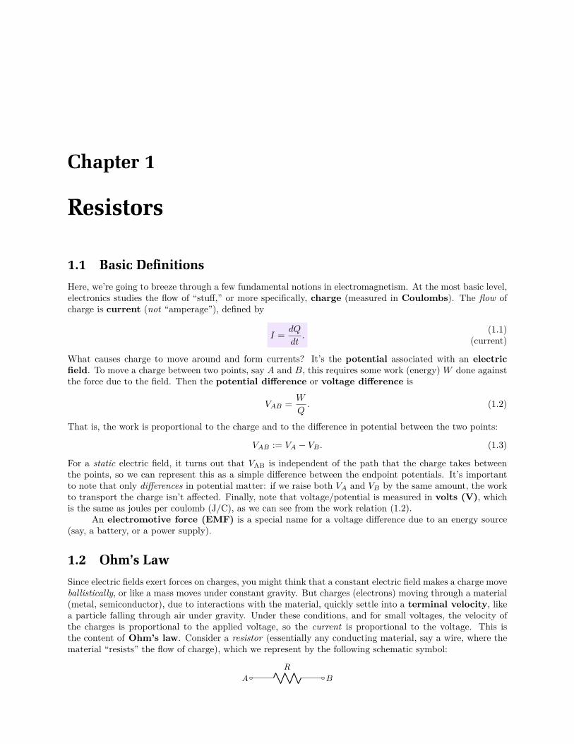
Since electric fields exert forces on charges, you might think that a constant electric field makes a charge moveballistically, or like a mass moves under constant gravity. But charges (electrons) moving through a material(metal, semiconductor), due to interactions with the material, quickly settle into a terminal velocity, likea particle falling through air under gravity. Under these conditions, and for small voltages, the velocity ofthe charges is proportional to the applied voltage, so the current is proportional to the voltage. This isthe content of Ohm’s law. Consider a resistor (essentially any conducting material, say a wire, where thematerial “resists” the flow of charge), which we represent by the following schematic symbol:
A
R
B

24 Chapter 1. Resistors
Here the resistance (measured in ohms or Ω) is R, and the resistor connects points A and B. Then Ohm’slaw states
VAB = IR.(1.4)
(Ohm’s law)
That is, for a fixed voltage, the current is inversely proportional to the resistance, which is sensible.The voltage (and hence, electric field) does work on the charges. The power is the rate of work, or
P =dW
dt. (1.5)
From Eq. (1.2), W = V Q (dropping subscripts on V ), and at constant voltage,
P = VdQ
dt= V I.
(1.6)(electrical power)
Of course, with Ohm’s law, we can also write
P = V I = I2R =V 2
R
(1.7)(electrical power)
for a few useful alternate forms of the electrical power
1.2.1 Resistors
Essentially anything short of a superconductor has resistance. Wires that carry current have resistance,but usually it’s desirable to keep their resistance small. But in virtually all electronic circuits, it’s useful tointroduce controlled quantities of resistance, and these are the electrical components we call resistors. A fewbasic types are:
1. wirewound resistors: are just wires wrapped around a form. These are usually expensive, but canbe precise (using thin wire to make a large resistor) or able to handle high power (using thick wireembedded in ceramic).
2. carbon film: are a thin layer of carbon deposited on some insulating form (usually a small cylinder).They’re cheap, but not particularly accurate in value. In the type with axial leads, these are usuallyrecognizable by their tan color.
3. metal film: are a thin layer of metal deposited on some insulating form (again, usually a smallcylinder). They’re more expensive than carbon, but more accurate. In the type with axial leads, theseare usually recognizable by a blue or blue/green color.
1.3 Networks and Kirchoff’s Laws
A simple circuit is any network of resistors, batteries, and wires (later to include more stuff!). There aretwo basic laws that govern the circuit if all we have is batteries and resistors, and these are called Kirchoff’slaws, on for current, and one for voltage.
1. The current law states that at any junction, the current going in to the junction must exactly balancethe current going out, for charge not to accumulate there:
∑
j
Iin,j =∑
j
Iout,j . (1.8)
We can also keep track of the sense of “in” and “out” by keeping track of the sign of the current (alwaysimportant to do!). Thus, for example, in the following junction,

1.3 Networks and Kirchoff’s Laws 25
I1 I2
I3
we should writeI1 + I2 + I3 = 0. (1.9)
On the other hand, if we draw the currents like this,
I1
I2
I3
then we should writeI1 − I2 + I3 = 0. (1.10)
2. The voltage law states that around a closed circuit or loop in a circuit, the EMFs must balance thevoltage drops, or
∑
j
Ej =∑
j
Vj , (1.11)
where the Ej are the EMFs, and the Vj are the voltage drops. For example, in the circuit below, theEMF is V due to the battery, so the voltage drop across the resistor must also be V .
V R
1.3.1 Series Resistors
Two resistors in series are the same as a single resistor, with an effective resistance that is the sum of theindividual resistors.
R1 R2
=
Reff = R1 + R2
Why? (Try to work this out on your own!)The idea is that any current I that flows through one must flow through the other. So the voltages
across the resistors are V1 = IR1 and V2 = IR2. Then the total drop across both resistors is
V = V1 + V2 = I(R1 + R2) =: IReff . (1.12)
Thus,Reff = R1 + R2 (1.13)
is the effective resistance of the series pair. Of course, this generalizes to multiple resistors.

26 Chapter 1. Resistors
1.3.2 Parallel Resistors
Two resistors in parallel also behave as a single resistor, as shown below.
R1
R2 =
Reff = R1‖R2
The shorthand notation here is1
R1‖R2:=
1
R1+
1
R2, (1.14)
so that more parallelism in resistors decreases resistance.Why is this? In this case, the voltage V is common to the two resistors. The currents are I1 = V/R1
and I2 = V/R2. But the total current through the pair must be I = I1 + I2, which satisfies I = V/Reff . Thismeans
V
Reff=
V
R1+
V
R2, (1.15)
and canceling the voltage gives1
Reff=
1
R1+
1
R2, (1.16)
which agrees with the shorthand above.
1.3.3 Voltage Divider
This is a useful combination of resistors that occurs all the time in circuits.
Vin
R1
R2
Vout
Here at the bottom of the circuit diagram, we are drawing the ground symbol, which means we are declaringthis point to be a fixed voltage (say, zero), and all other voltages are differences with respect to ground. (Inthe “ground” or “earth” pin on an ac power receptacle, this is literally the ground outside. Often the caseof electrical devices is connected to ground for safety, and in cars the entire chassis is ground.)
Now due to the input voltage Vin, some current flows in from the input. This must satisfy
I =Vin
R1 + R2. (1.17)
The same current flows through R2, so
Vout = IR2 =
(
R2
R1 + R2
)
Vin.(1.18)
(voltage divider)
The output voltage is reduced from the input by the ratio of R2 to the total resistance. This is important;you should memorize this. Especially if this is made from an adjustable resistor (potentiometer), thiscan be used to make an adjustable voltage source.
However, suppose we chain two voltage dividers, as follows.

1.4 Thévenin’s Theorem 27
Vin
R
R R
R
Vout
Is the output voltage just divided twice, or 1/4 the input voltage? Why not?
1.4 Thévenin’s Theorem
Thévenin’s theorem1 is very useful in analyzing passive networks. It says that any network of resistors andEMFs—if we interact with it only at two points—can be replaced by an equivalent circuit of a series EMFand resistor, as shown.
RThVTh
Vout
The EMF and resistance are called the Thévenin equivalent voltage and Thévenin equivalent resis-tance, respectively. This equivalent circuit is a direct consequence of the linearity of a passive network. Wewill defer the proof to Section 1.5.4 because it is fairly technical and not necessary for understanding it; fornow we’ll concentrate on making good use of it.
How do we find the Thévenin equivalent component values? A couple of observations:
1. If nothing is connected to the output, then Vout = VTh.
2. If the output is short-circuited,2 then Vout = 0 and VTh = RThIshort.
These allow you to infer the Thévenin values. The second rule is useful experimentally, provided shortingthe output does not destroy the circuit!
An alternate rule to find the Thévenin resistance, especially in analyzing a circuit on paper, isas follows.
2. (alternate rule) Replace all EMFs by short circuits, and compute the equivalent resistance at theoutput.
This is, in fact, typically the more useful version of rule 2.
1Named for L. Thévenin, “Extension de la loi d’Ohm aux circuits électromoteurs complexes,” Annales Télégraphiques(Troisieme série) 10, 222 (1883); L. Thévenin, “Sur un nouveau théorème d’électricité dynamique,” Comptes Rendus Heb-domadaires des Séances de l’Académie des Sciences 97, 159 (1883). For a historical overview as well as an English translationof part of Thévenin’s papers, see Don H. Johnson, “Origins of the Equivalent Circuit Concept: The Voltage-Source Equiva-lent,” Proceedings of the IEEE 91, 636 (2003) (doi: 10.1109/JPROC.2003.811716) https://pdfs.semanticscholar.org/b55d/
3f11daa8943d76fbe645b13020d4b1602648.pdf. The proof as mentioned by Johnson is a very brief version of the one we presentin Section 1.5.4.
2A “short circuit” or “short” is a direct, low-resistance path between two points in a circuit, like a piece of wire. It acts likea “shortcut” for current between the two points, compared to going through the regular, higher-resistance paths in the circuit.

28 Chapter 1. Resistors
1.4.1 Voltage Divider
Back to the voltage divider of Section 1.3.3.
Vin
R1
R2
Vout
1. We already found the Thévenin voltage as the unloaded-output voltage:
VTh =
(
R2
R1 + R2
)
Vin.(1.19)
(voltage divider, Thévenin voltage)
2. If we short the output (to ground), the current only flows through R1, so Ishort = Vin/R1. Then usingRTh = VTh/Ishort, we get
RTh =R1R2
R1 + R2= R1‖R2.
(voltage divider, Thévenin resistance) (1.20)
That is, the equivalent circuit is as below
RThVTh
Vout
The equivalent voltage is the divided voltage, and the equivalent resistance is the parallel resistance ofthe two resistors. This is important; you should memorize this. This result also follows directly fromthe alternative rule: replacing Vin with a short to ground just puts R1 and R2 in parallel from the point ofview of the output.
Now back to the example of two cascaded voltage dividers.
Vin
R
R R
R
Vout
1.4 Thévenin’s Theorem 29
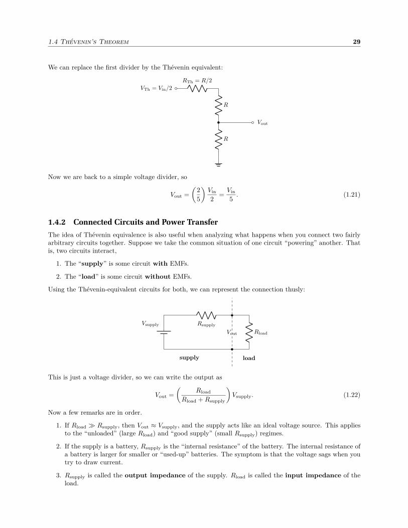
We can replace the first divider by the Thévenin equivalent:
VTh = Vin/2
RTh = R/2
R
R
Vout
Now we are back to a simple voltage divider, so
Vout =
(
2
5
)
Vin
2=
Vin
5. (1.21)
1.4.2 Connected Circuits and Power Transfer
The idea of Thévenin equivalence is also useful when analyzing what happens when you connect two fairlyarbitrary circuits together. Suppose we take the common situation of one circuit “powering” another. Thatis, two circuits interact,
1. The “supply” is some circuit with EMFs.
2. The “load” is some circuit without EMFs.
Using the Thévenin-equivalent circuits for both, we can represent the connection thusly:
RsupplyVsupply
Vout Rload
supply load
This is just a voltage divider, so we can write the output as
Vout =
(
Rload
Rload + Rsupply
)
Vsupply. (1.22)
Now a few remarks are in order.
1. If Rload ≫ Rsupply, then Vout ≈ Vsupply, and the supply acts like an ideal voltage source. This appliesto the “unloaded” (large Rload) and “good supply” (small Rsupply) regimes.
2. If the supply is a battery, Rsupply is the “internal resistance” of the battery. The internal resistance ofa battery is larger for smaller or “used-up” batteries. The symptom is that the voltage sags when youtry to draw current.
3. Rsupply is called the output impedance of the supply. Rload is called the input impedance of theload.

30 Chapter 1. Resistors
4. The impedance-matching condition answer, under what conditions is maximum power transferredfrom source to load? The power in the load is
Pload =V 2
out
Rload=
Rload
(Rload + Rsupply)2V 2
supply. (1.23)
Maximizing this viad
da
(
a
(a + b)2
)
=1
(a + b)2− 2a
(a + b)3= 0, (1.24)
which leads to a = b, we have the matching condition
Rload = Rsupply.(1.25)
(impedance-matching condition)
This is saying, for a fixed source impedance, the most power we can get out of the source and into theload is if the load impedance matches the supply impedance. In older tube amplifiers, this was an im-portant consideration. For efficient matching to different speaker loads, amplifier output transformerswould often have different “taps” for 4 Ω, 8 Ω, 16 Ω, etc. speakers.
1.5 Matrix Solution of Resistor Networks
Have a look at the XKCD comic “Circuit Diagram,”3 and enjoy (you’ll recognize more stuff here as youlearn more about electronics). Make sure to hover the cursor over the comic so you see the last joke.
Now look at part of the circuit labelled “Oh, so you think you’re such a whiz at EE 201?” (If you can’taccess the circuit for whatever reason, it is a rat’s next of resistors, and the idea is to find the equivalentresistance.) Randall Munroe was joking, but we’ll develop a systematic way to handle this kind of problem,which you can use to tackle that mess without much difficulty.
1.5.1 Review of Linear Algebra
First, we’re going to use some linear algebra (in practice, we will want the help of a computer), so let’sreview the notation. A matrix is a group of numbers indexed by two numbers. For example, we can writedown a 2× 2 matrix as
[
A11 A12
A21 A22
]
. (1.26)
We can refer to the whole matrix as A. We can also refer an element (one of the entries) of the matrix asAij . Note that i refers to the element’s row, while j refers to the element’s column. We can write a systemof linear equations as
[
A11 A12
A21 A22
] [
x1
x2
]
=
[
b1
b2
]
. (1.27)
This is just another way to write down the pair of equations
A11x1 + A12x2 = b1
A21x1 + A22x2 = b2
(1.28)
and the shorthand notation for the matrix form is
Ax = b, (1.29)
where x and b are vectors (i.e., n×1 matrices, or specifically here, 2×1 matrices). Under certain conditions,it is possible to solve for the xj in terms of the bi and the Aij (we’ll let a computer help here). Make sureyou understand the pattern of the matrix-vector multiplication in the equations above before you continue.
3http://xkcd.com/730/
1.5 Matrix Solution of Resistor Networks 31
1.5.2 Matrix Form of the Resistance Network and Example
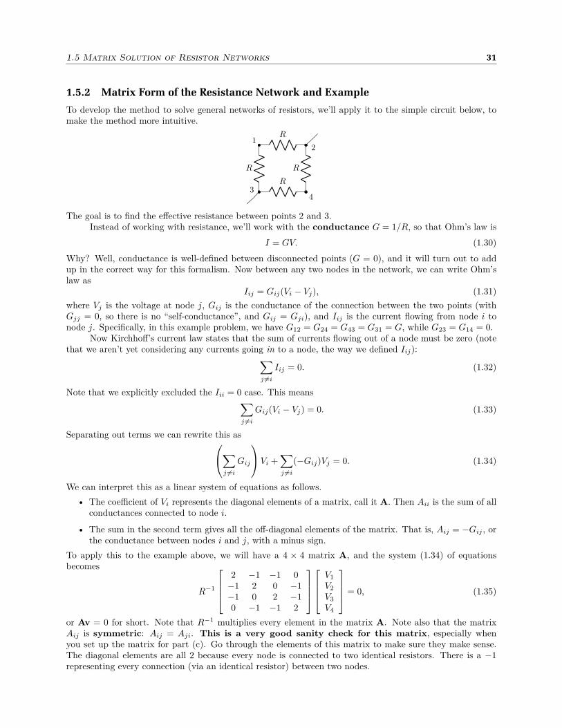
To develop the method to solve general networks of resistors, we’ll apply it to the simple circuit below, tomake the method more intuitive.
R
R
R
R
12
34
The goal is to find the effective resistance between points 2 and 3.Instead of working with resistance, we’ll work with the conductance G = 1/R, so that Ohm’s law is
I = GV. (1.30)
Why? Well, conductance is well-defined between disconnected points (G = 0), and it will turn out to addup in the correct way for this formalism. Now between any two nodes in the network, we can write Ohm’slaw as
Iij = Gij(Vi − Vj), (1.31)
where Vj is the voltage at node j, Gij is the conductance of the connection between the two points (withGjj = 0, so there is no “self-conductance”, and Gij = Gji), and Iij is the current flowing from node i tonode j. Specifically, in this example problem, we have G12 = G24 = G43 = G31 = G, while G23 = G14 = 0.
Now Kirchhoff’s current law states that the sum of currents flowing out of a node must be zero (notethat we aren’t yet considering any currents going in to a node, the way we defined Iij):
∑
j 6=i
Iij = 0. (1.32)
Note that we explicitly excluded the Iii = 0 case. This means∑
j 6=i
Gij(Vi − Vj) = 0. (1.33)
Separating out terms we can rewrite this as
∑
j 6=i
Gij
Vi +∑
j 6=i
(−Gij)Vj = 0. (1.34)
We can interpret this as a linear system of equations as follows.
• The coefficient of Vi represents the diagonal elements of a matrix, call it A. Then Aii is the sum of allconductances connected to node i.
• The sum in the second term gives all the off-diagonal elements of the matrix. That is, Aij = −Gij , orthe conductance between nodes i and j, with a minus sign.
To apply this to the example above, we will have a 4 × 4 matrix A, and the system (1.34) of equationsbecomes
R−1
2 −1 −1 0−1 2 0 −1−1 0 2 −10 −1 −1 2
V1
V2
V3
V4
= 0, (1.35)
or Av = 0 for short. Note that R−1 multiplies every element in the matrix A. Note also that the matrixAij is symmetric: Aij = Aji. This is a very good sanity check for this matrix, especially whenyou set up the matrix for part (c). Go through the elements of this matrix to make sure they make sense.The diagonal elements are all 2 because every node is connected to two identical resistors. There is a −1representing every connection (via an identical resistor) between two nodes.

32 Chapter 1. Resistors
1.5.3 Solution for the Effective Resistance
Unfortunately, the above matrix equation is not useful as is, because it is satisfied by Vi = V for any constantV . Physically, without any applied voltage, this circuit really doesn’t do much. But first, we’ll take care ofanother problem: the matrix A is singular, meaning one of the equations in the linear system is redundant.Physically, this is because the absolute voltage of the circuit is not defined (the equations, by construction,only determine voltage differences). We can fix this by explicitly tying one of the nodes to zero voltage.Since node 3 is one of the nodes of interest, let’s set
V3 = 0, (1.36)
which means we replace one of the equations in the linear system by this one. In matrix form, we will modifythe third row of the matrix as follows:
R−1
2 −1 −1 0−1 2 0 −10 0 1 00 −1 −1 2
V1
V2
V3
V4
= 0. (1.37)
To solve the other problem (i.e., to make the circuit do something), let’s introduce a current I, which flowsinto node 2. The same current I must flow out of node 3.
R
R
R
R
12
34
I
I
To handle this, we will modify Eq. (1.34) to say that the sum of currents flowing out of a node is equal tothe currents flowing into a node (counting the external currents I as inputs, with minus signs to properlyreflect their direction):
∑
j 6=i
Gij
Vi +∑
j 6=i
(−Gij)Vj = Iin,i. (1.38)
Here Iin,i is the current flowing in to node i. In our example problem, Iin,2 = I, while Iin,3 = −I. Nowwriting the linear system including these currents, we have
2 −1 −1 0−1 2 0 −10 0 1 00 −1 −1 2
V1
V2
V3
V4
=
0IR00
. (1.39)
Note that we kept the third row of the matrix to reflect V3 = 0, and we only introduced the current I atnode 2. This is a well-defined system of equations, which we can solve to obtain V2. The effective resistanceof the network is defined by
Reff =V2 − V3
I=
V2
I. (1.40)
When you solve the matrix equation, as you might expect, the result should be Reff = R. We will leave thedetails and the application to the XKCD problem to an exercise (Problem 1.20).
1.5 Matrix Solution of Resistor Networks 33
1.5.4 Proof of Thévenin’s Theorem
A slightly more general version of the above matrix formalism for resistor networks allows us to proveThévenin’s theorem. Recall that the theorem dealt with networks of resistors and EMFs; first let’s handlethe resistors and then put the EMFs in later.
But before proceeding it is useful to recast the above matrix formalism as an optimization problem.To do this, we can begin by noting that the resistor connecting nodes i and j dissipates a power
Pij = Iij(Vi − Vj) = Gij(Vi − Vj)2, (1.41)
where we used Eq. (1.31) in the last step. Summing over all resistors, we can then write the total power as
P =∑
i,j<i
Pij =∑
i,j<i
Gij(Vi − Vj)2 =∑
i,j≤i
Gij(Vi − Vj)2, (1.42)
where we are taking advantage of the definition Gjj = 0 for any j. So far, we are being careful to count anyresistor only once, but we are free to double-count provided we divide the result by two. Thus,
P (v) =1
2
∑
i,j
Gij(Vi − Vj)2, (1.43)
where we are explicitly regarding the power to be a function of the voltage “coordinate vector” v =(V1, V2, . . . , VN ). The solution corresponds to a minimum in P in the sense that the vanishing-gradientcondition ∇P (v) = 0 gives
∂P
∂Vi=∑
j
Gij(Vi − Vj) = 0. (1.44)
This is just the Kirchoff current law in the form (1.33), which we used to set up the matrix solution of ageneral resistor network above. Intuitively, the circuit voltages (and currents) will arrange themselves in sucha way as to minimize the power dissipated in the network, subject to any constraints on the network, suchas applied voltages. (Technically, we have only showed that the power is stationary with respect to voltagechanges, and thus could correspond to a saddle point or even a maximum, though minimization of poweris nicely intuitive.) It is the constraints that we will now have to deal with explicitly to tackle Thévenin’stheorem.
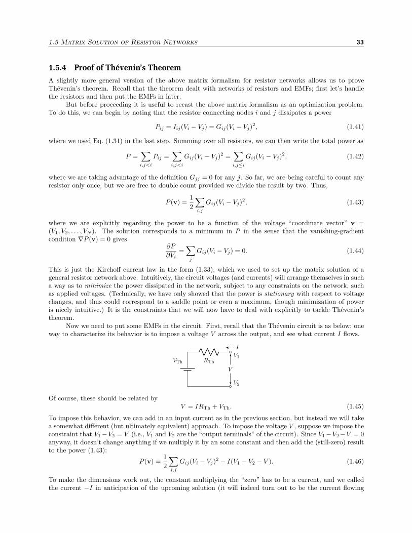
Now we need to put some EMFs in the circuit. First, recall that the Thévenin circuit is as below; oneway to characterize its behavior is to impose a voltage V across the output, and see what current I flows.
I
V1
V2
RThVTh
V
Of course, these should be related byV = IRTh + VTh. (1.45)
To impose this behavior, we can add in an input current as in the previous section, but instead we will takea somewhat different (but ultimately equivalent) approach. To impose the voltage V , suppose we impose theconstraint that V1−V2 = V (i.e., V1 and V2 are the “output terminals” of the circuit). Since V1−V2−V = 0anyway, it doesn’t change anything if we multiply it by an some constant and then add the (still-zero) resultto the power (1.43):
P (v) =1
2
∑
i,j
Gij(Vi − Vj)2 − I(V1 − V2 − V ). (1.46)
To make the dimensions work out, the constant multiplying the “zero” has to be a current, and we calledthe current −I in anticipation of the upcoming solution (it will indeed turn out to be the current flowing

34 Chapter 1. Resistors
via the output terminals). However, technically at this point it is an undetermined constant, and theconstraint equation V1 − V2 − V = 0 along with the ∇P (V) = 0 equations will allow us to determine I. Inoptimization-theory parlance, I is called a Lagrange multiplier.
To add in the other EMFs in the resistor network, the idea proceeds by adding constraints in the sameway. Suppose we add in a bunch of different EMFs Ek connecting various pairs of network nodes. Theseconstraints can be represented by vanishing constraint functions
fk(v) = Vσ(k) − Vτ(k) − Ek = 0, (1.47)
which imposes the EMF Ek between the σ(k)th and τ(k)th nodes, where σ(k) and τ(k) are indexing functionsthat simply track the node placement of the kth EMF. At most, with N total voltage nodes, there can beN−2 more constraint EMFs (in addition to the one we already imposed) without overconstraining the circuit.(We otherwise won’t worry about inconsistent constraints, and we can note that in the case where the outputnodes should be voltage-constrained by an EMF that is part of the circuit, the resulting Thévenin circuitis trivial, so we won’t worry about that case here.) Introducing extra Lagrange multipliers Ik, Eq. (1.46)becomes
P (v) =1
2
N∑
i,j=1
Gij(Vi − Vj)2 − I(V1 − V2 − V )−NC≤N−2∑
k=1
Ik(Vσ(k) − Vτ(k) − Ek). (1.48)
after implementing all the EMFs as constraints. Here NC ≤ N − 2 is the number of constraints (EMFs).Now differentiating Eq. (1.48) with respect to Vi leads to the system of equations
N∑
j=1
Gij(Vi − Vj)− I(δi,1 − δi,2)−NC≤N−2∑
k=1
Ik(δi,σ(k) − δi,τ(k)) = 0, (1.49)
where δnm is the Kronecker delta, satisfying δnn = 1 and δnm = 0 whenever n 6= m. If we rearrange the firstsum as in Eq. (1.34), this becomes
N∑
j=1
Gij
Vi +N∑
j=1
(−Gij)Vj −NC≤N−2∑
k=1
Ik(δi,σ(k) − δi,τ(k)) = I(δi,1 − δi,2), (1.50)
and comparison with Eq. (1.38) shows that the Lagrange multipliers indeed have the interpretation as extracurrents into the respective nodes. In particular the Ik are the currents supplied by the corresponding EMFsEk in order to maintain their imposed voltages within the network.
The N equations (1.50), along with the constraint equations (1.47) in the form
Vσ(k) − Vτ(k) = Ek, (1.51)
with V1−V2 = V , give N +NC +1 equations for the N +NC +2 variables (V, V1, . . . , VN , I, I1, . . . , INC). How-
ever, recall that the system represented by 1.50 is singular in the sense that one is redundant, correspondingphysically to the ambiguity of the absolute voltage. We can cure this by replacing one of the equations, sayi = 2, by the condition V2 = 0. Assuming this has been done, we can simply implement V1 − V2 = V byreplacing V1 by V , and the we can write the above N + NC remaining equations as
Gv = Ie1 + ǫ, (1.52)
where v has been extended to include the Lagrange-multiplier currents as v := (V, V2, . . . , VN , I1, . . . , INC);
G is a square matrix encoding the left-hand sides of the Kirchoff and EMF-constraint equations; e1 is theunit vector (1, 0, 0, . . . , 0); and ǫ := (0, 0, . . . , 0, E1, . . . , ENC
) This system has the solution
v = (G−1e1)I + G−1ǫ, (1.53)
Recall that the first equation is the equation determining V . Thus, the most relevant solution for ourpurposes is
V = e1 · (G−1e1)I + e1 · (G−1ǫ),(1.54)
(Thévenin’s theorem)
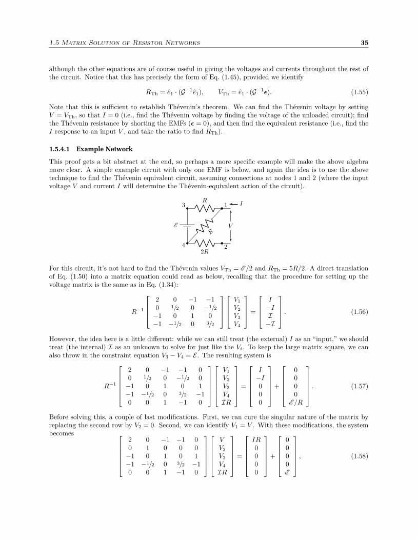
1.5 Matrix Solution of Resistor Networks 35
although the other equations are of course useful in giving the voltages and currents throughout the rest ofthe circuit. Notice that this has precisely the form of Eq. (1.45), provided we identify
RTh = e1 · (G−1e1), VTh = e1 · (G−1ǫ). (1.55)
Note that this is sufficient to establish Thévenin’s theorem. We can find the Thévenin voltage by settingV = VTh, so that I = 0 (i.e., find the Thévenin voltage by finding the voltage of the unloaded circuit); findthe Thévenin resistance by shorting the EMFs (ǫ = 0), and then find the equivalent resistance (i.e., find theI response to an input V , and take the ratio to find RTh).
1.5.4.1 Example Network
This proof gets a bit abstract at the end, so perhaps a more specific example will make the above algebramore clear. A simple example circuit with only one EMF is below, and again the idea is to use the abovetechnique to find the Thévenin equivalent circuit, assuming connections at nodes 1 and 2 (where the inputvoltage V and current I will determine the Thévenin-equivalent action of the circuit).
I
E
R
2R
R
3 1
4 2
V
For this circuit, it’s not hard to find the Thévenin values VTh = E /2 and RTh = 5R/2. A direct translationof Eq. (1.50) into a matrix equation could read as below, recalling that the procedure for setting up thevoltage matrix is the same as in Eq. (1.34):
R−1
2 0 −1 −10 1/2 0 −1/2
−1 0 1 0−1 −1/2 0 3/2
V1
V2
V3
V4
=
I−II−I
. (1.56)
However, the idea here is a little different: while we can still treat (the external) I as an “input,” we shouldtreat (the internal) I as an unknown to solve for just like the Vi. To keep the large matrix square, we canalso throw in the constraint equation V3 − V4 = E . The resulting system is
R−1
2 0 −1 −1 00 1/2 0 −1/2 0−1 0 1 0 1−1 −1/2 0 3/2 −10 0 1 −1 0
V1
V2
V3
V4
IR
=
I−I000
+
0000
E /R
. (1.57)
Before solving this, a couple of last modifications. First, we can cure the singular nature of the matrix byreplacing the second row by V2 = 0. Second, we can identify V1 = V . With these modifications, the systembecomes
2 0 −1 −1 00 1 0 0 0−1 0 1 0 1−1 −1/2 0 3/2 −10 0 1 −1 0
VV2
V3
V4
IR
=
IR0000
+
0000E
, (1.58)

36 Chapter 1. Resistors
and it’s ready to solve. Inverting the matrix G gives
G−1 =
5/2 1 2 2 1/2
0 1 0 0 02 1 2 2 12 1 2 2 0
1/2 0 1 0 −1/2
, (1.59)
and thus the solution
VV2
V3
V4
IR
= G−1
IR0000
+ G−1
0000E
= I
(5/2)R0
2R2R
(1/2)R
+
1/2
010−1/2
E . (1.60)
Reading off the top equation gives the Thévenin parameters,
V = I
(
5R
2
)
+E
2, (1.61)
so that RTh = 5R/2 and VTh = E /2, as expected. The other rows in the linear system give more information;for example the last equation gives I = IR/2− E /2 for the current through the EMF. The other rows giveV4 = 2IR and V3 = E + 2IR, which are both readily apparent from looking at the circuit diagram.
1.5.4.2 Extension to Current Sources
In the proof above, we only considered a network of EMFs (ideal voltage sources) and resistors. However,Thévenin’s theorem still works if you throw in a few current sources. We have already seen how to do thisin Eq. (1.38), where an external “input” current flows into one node and out another. In terms of the powerequation (1.48), we accomplished this same effect by inserting a constraint term −I(V1 − V2 − V ), whichconstrained V12 = V by imposing whatever input current I achieves this. The same idea can work to put inother current sources. Adding a term of the form −Is(Vi − Vj − Vij) does this if we view it correctly: if weregard Vij as an unknown, it will simply take on the value Vi − Vj while introducing the source current Is
between nodes i and j. The upshot is that Eq. (1.50) becomes
N∑
j=1
Gij
Vi +
N∑
j=1
(−Gij)Vj−NC≤N−2∑
k=1
Ik(δi,σ(k)−δi,τ(k)) = I(δi,1−δi,2)+
NI∑
k=1
Isk(δi,σ′(k)−δi,τ ′(k)), (1.62)
where there are NI current sources, with the kth source between nodes σ′(k) and τ ′(k). Note that thesecurrent sources are not real constraints; they simply redirect current through the circuit, and thus there isin principle no limit to how many current sources we can have.
These extra current sources can be collected in the same way as I, so that Eq. (1.52) becomes
Gv = Ie1 + ǫ + ι, (1.63)
where the ith entry in ι is the sum of all source currents into node i, minus the sum of all source currentsout of the same node. The matrix system has the more general solution
v = (G−1e1)I + G−1ǫ + G−1ι, (1.64)
and the first equation of this linear system is
V = e1 · (G−1e1)I + e1 · (G−1ǫ) + e1 · (G−1ι),
(Thévenin’s theorem with current sources) (1.65)

1.5 Matrix Solution of Resistor Networks 37
Thus, we have the same theorem, but with a modified Thévenin voltage:
RTh = e1 · (G−1e1), VTh = e1 · [G−1(ǫ + ι)]. (1.66)
Note that it looks like we are conflating units, especially in the Thévenin voltage, but note that by construc-tion the ǫ and ι vectors cannot have nonzero entries in the same position.
The procedure for handling current sources in applying Thévenin’s theorem is the same: To find theThévenin voltage, find the unloaded output voltage; to find the Thévenin resistance, find the resistance withall EMFs replaced by short circuits and all current sources replaced by open circuits (corresponding to azero currents).
1.5.4.3 Norton’s Theorem
Incidentally, there is another possible equivalent circuit that serves as an alternative to the Thévenin circuit.Consider the following circuit, analogous to the Thévenin circuit (p. 33).
I
V1
V2
RN
IN
V
Here, both the source current IN and the external current I flow through RN, and thus
V = IRN + INRN. (1.67)
Note that Eq. (1.65) has this form and thus the proof for Thévenin’s theorem also shows that this current-source circuit is also an equivalent representation, with the identifications
RN = e1 · (G−1e1), IN =e1 · [G−1(ǫ + ι)]
e1 · (G−1e1). (1.68)
This is called Norton’s theorem,4 and the procedure for finding the elements of the equivalent circuit isanalogous to the Thévenin procedure:
1. With the output short-circuited, calculate the output current Ishort, which is just IN.
2. With the output unloaded, compute the output voltage, which gives RN via Vout = V = INRN.
2. (alternate rule) Replace voltage sources by short circuits and current sources by open circuits, thencalculate the equivalent resistance across the output terminals to get RN.
In fact, comparing Eq. (1.67) to Eq. (1.45), it is easy to convert between a Thévenin and a Nortonequivalent circuit by identifying
RTh = RN, VTh = INRN.(1.69)
(Thévenin–Norton conversion)
In practice, the Thévenin circuit seems to be the more useful representation, but it’s still handy to knowabout the Norton equivalent.
4Named after E. L. Norton, “Design of finite networks for uniform frequency characteristic, Technical Report TM26?0?1860,Bell Laboratories, 1926. This theorem is also called the Mayer–Norton theorem, after H. F. Mayer, “Über das Ersatzschemader Verstärkerröhre,” Telegraphen- und Fernsprech-Technik 15, 335 (1926). For a nice history, see Don H. Johnson, “Ori-gins of the Equivalent Circuit Concept: The Current-Source Equivalent,” Proceedings of the IEEE 91, 817 (2003) (doi:10.1109/JPROC.2003.811795) https://pdfs.semanticscholar.org/8b43/8720d7d7773d2a2b599932648878c84d40e2.pdf.

38 Chapter 1. Resistors
1.5.4.4 Superposition of Sources
One final observation regarding Eq. (1.65) is in order here. The source vectors ǫ and ι for EMFs and currentsources, respectively, can be decomposed into sums of vectors, each corresponding to a single source. Thetotal effect on V is simply a sum over terms involving each source (including I). The interpretation of thisis, that if we know the value of V when we “turn on” only one source at a time, we can simply sum up allthese voltages to find the value of V when all the sources are present together. The same conclusion holdsfor the current between two nodes, assuming they are not connected by a voltage source. This is sometimescalled the superposition theorem, and is sometimes useful in analyzing linear circuits. (It is sometimesalso used as the justification for Thévenin’s theorem.)

1.6 Circuit Practice 39
1.6 Circuit Practice
Here are a few example circuits to analyze with solutions; try to work these out and test your understandingso far. (Try before looking at the solutions!)
1.6.1 Reflection-Symmetric Network
Given that all resistors here are equal and of resistance R, what is the equivalent resistance between A andB?
A
B
Solution. Notice that by symmetry, the voltage across the center resistance is zero, so the current flowingthrough it is zero, no matter what the voltage VAB . Thus, we can remove it from the circuit. The same goesfor the two other “equatorial” resistors. Thus, we have 4 parallel resistances of 2R, for a total resistanceR/2.
1.6.2 Series and Parallel Light Bulbs
Suppose the three bulbs in the circuit below are identical.
A
B
C
What is the relative brightness of the bulbs? Do bulbs B and C get brighter or dimmer when you removeA?
Solution. First, note that half the C current flows through A and B, while A and B drop half the voltageof C. So A and B are 1/4 as bright as C.
When A is removed, then B and C are equally bright. Less current flows overall, because the totalresistance is larger. C drops less voltage than it used to, B drops more than it used to. Clearly C should bedimmer, but B should be brighter, because it now has more voltage and more current (the drop in overallcurrent is outweighed by the factor of 2 this bulb gets by its neighbor disappearing).
To be careful, note in the original case that the voltage across C is (2/3)V , and across A and B it is(1/3)V , where V is the battery voltage. The current through C is (2/3)V/R, and half that flows throughA and B. In the new case, each bulb drops V/2, and current (1/2)V/R flows through each. Before, the Cpower was the product of voltage and current, or (4/9)V 2/R, and now it is (1/2)V 2/R, so this is dimmer.Before, the B power was (1/9)V 2/R, so this one gets brighter.
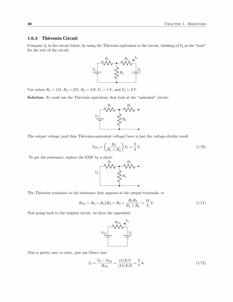
40 Chapter 1. Resistors
1.6.3 Thévenin Circuit
Compute I3 in the circuit below, by using the Thévenin equivalent to the circuit, thinking of V2 as the “load”for the rest of the circuit.
R1
R2
V1 V2
R3I3
Use values R1 = 1 Ω, R2 = 2 Ω, R3 = 4 Ω, V1 = 1 V, and V2 = 2 V.
Solution. To work out the Thévenin equivalent, first look at the “unloaded” circuit:
R1
R2
V1
R3
The output voltage (and thus Thévenin-equivalent voltage) here is just the voltage-divider result
VTh =
(
R2
R1 + R2
)
V1 =2
3V. (1.70)
To get the resistance, replace the EMF by a short:R1
R2
V1
R3
The Thévenin resistance is the resistance that appears at the output terminals, or
RTh = R3 + R1‖R2 = R3 +R1R2
R1 + R2=
14
3V. (1.71)
Now going back to the original circuit, we have the equivalent
VTh V2
RThI3
This is pretty easy to solve, just use Ohm’s law:
I3 =V2 − VTh
RTh=
(4/3) V
(14/3) Ω=
2
7A. (1.72)
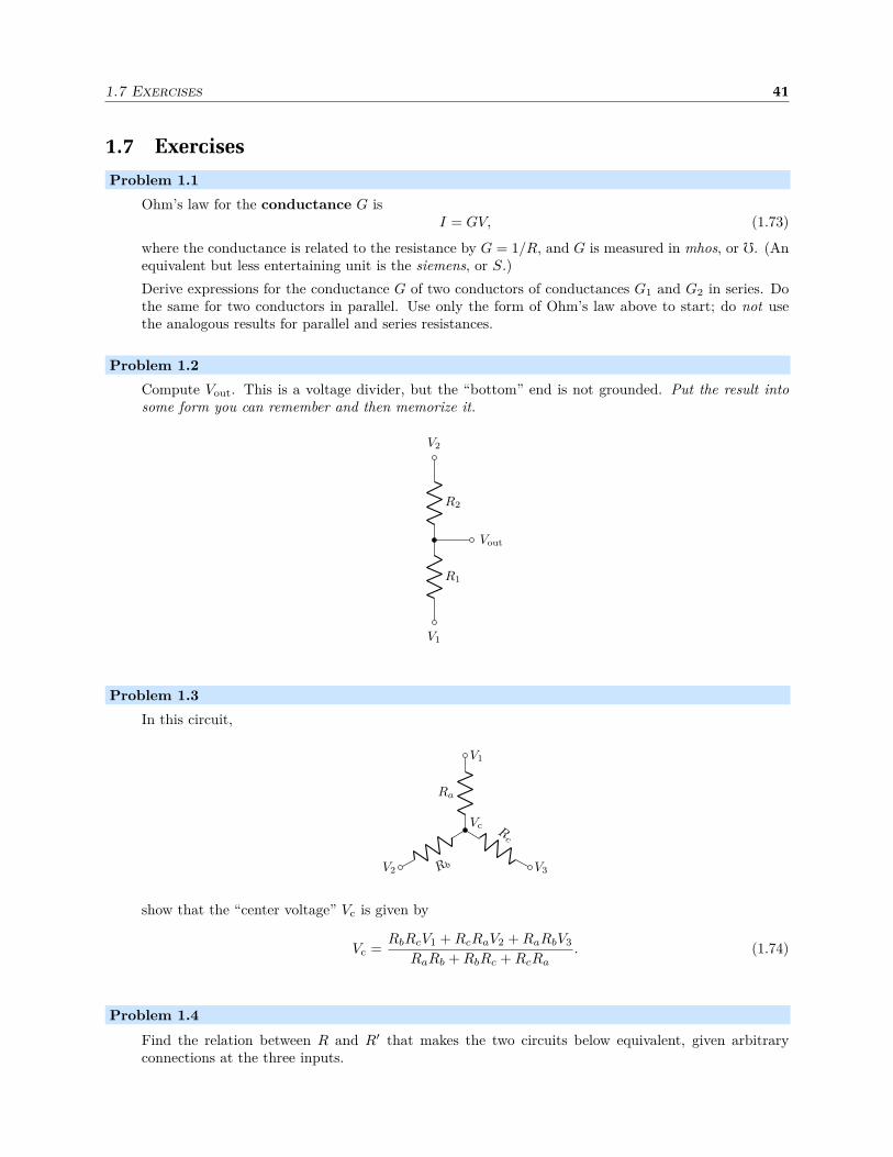
1.7 Exercises 41
1.7 Exercises
Problem 1.1
Ohm’s law for the conductance G isI = GV, (1.73)
where the conductance is related to the resistance by G = 1/R, and G is measured in mhos, or . (Anequivalent but less entertaining unit is the siemens, or S.)
Derive expressions for the conductance G of two conductors of conductances G1 and G2 in series. Dothe same for two conductors in parallel. Use only the form of Ohm’s law above to start; do not usethe analogous results for parallel and series resistances.
Problem 1.2
Compute Vout. This is a voltage divider, but the “bottom” end is not grounded. Put the result into
some form you can remember and then memorize it.
R2
R1
V2
V1
Vout
Problem 1.3
In this circuit,
Ra
V1
RbV2
Rc
V3
Vc
show that the “center voltage” Vc is given by
Vc =RbRcV1 + RcRaV2 + RaRbV3
RaRb + RbRc + RcRa. (1.74)
Problem 1.4
Find the relation between R and R′ that makes the two circuits below equivalent, given arbitraryconnections at the three inputs.
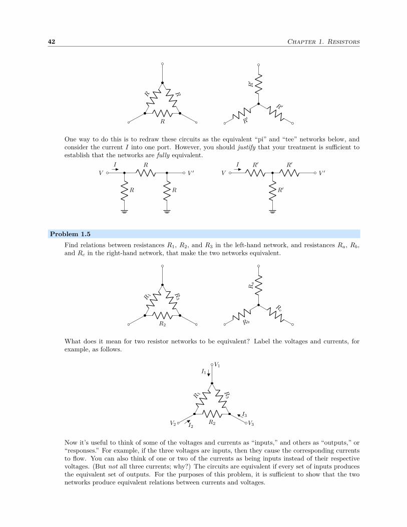
42 Chapter 1. Resistors
R
R
R
R′
R′
R ′
One way to do this is to redraw these circuits as the equivalent “pi” and “tee” networks below, andconsider the current I into one port. However, you should justify that your treatment is sufficient toestablish that the networks are fully equivalent.
I
V
R
R
R
V ′
I
V
R′
R′
R′
V ′
Problem 1.5
Find relations between resistances R1, R2, and R3 in the left-hand network, and resistances Ra, Rb,and Rc in the right-hand network, that make the two networks equivalent.
R1
R2
R3
Ra
Rb
Rc
What does it mean for two resistor networks to be equivalent? Label the voltages and currents, forexample, as follows.
R1
V1
R2V2
R3
V3
I1
I2
I3
Now it’s useful to think of some of the voltages and currents as “inputs,” and others as “outputs,” or“responses.” For example, if the three voltages are inputs, then they cause the corresponding currentsto flow. You can also think of one or two of the currents as being inputs instead of their respectivevoltages. (But not all three currents; why?) The circuits are equivalent if every set of inputs producesthe equivalent set of outputs. For the purposes of this problem, it is sufficient to show that the twonetworks produce equivalent relations between currents and voltages.
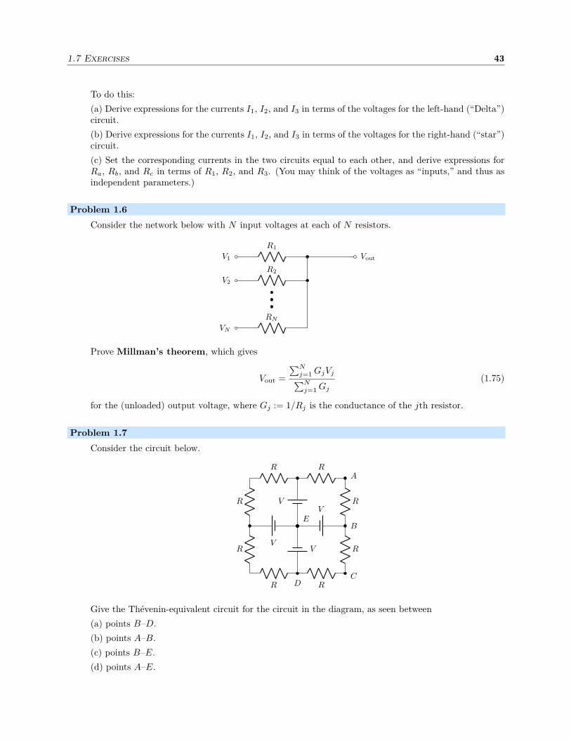
1.7 Exercises 43
To do this:
(a) Derive expressions for the currents I1, I2, and I3 in terms of the voltages for the left-hand (“Delta”)circuit.
(b) Derive expressions for the currents I1, I2, and I3 in terms of the voltages for the right-hand (“star”)circuit.
(c) Set the corresponding currents in the two circuits equal to each other, and derive expressions forRa, Rb, and Rc in terms of R1, R2, and R3. (You may think of the voltages as “inputs,” and thus asindependent parameters.)
Problem 1.6
Consider the network below with N input voltages at each of N resistors.
R1
R2
RN
VoutV1
V2
VN
Prove Millman’s theorem, which gives
Vout =
∑Nj=1 GjVj∑N
j=1 Gj
(1.75)
for the (unloaded) output voltage, where Gj := 1/Rj is the conductance of the jth resistor.
Problem 1.7
Consider the circuit below.
V
V
V
V
R
R
RR
R
R
R RA
B
CD
E
Give the Thévenin-equivalent circuit for the circuit in the diagram, as seen between
(a) points B–D.
(b) points A–B.
(c) points B–E.
(d) points A–E.
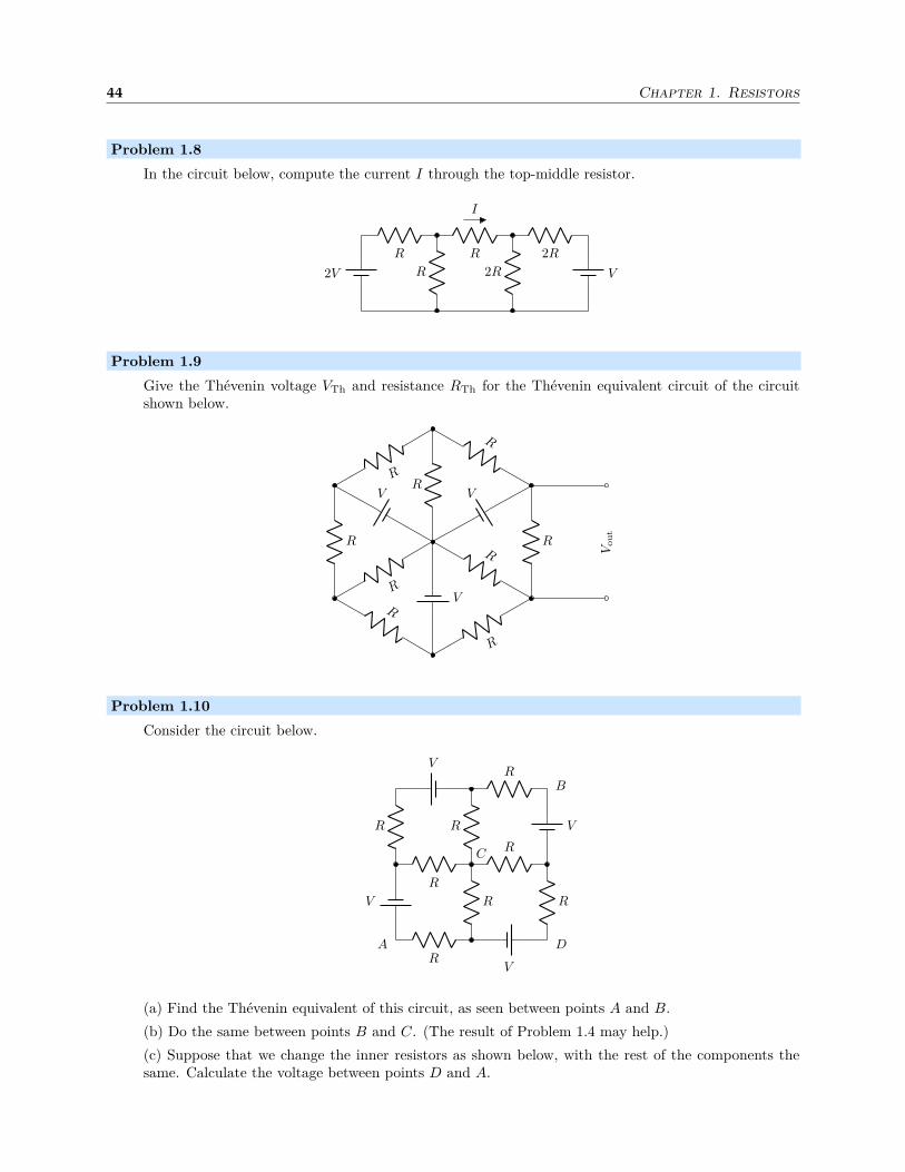
44 Chapter 1. Resistors
Problem 1.8
In the circuit below, compute the current I through the top-middle resistor.
V
2R
2R
R
R
R
2V
I
Problem 1.9
Give the Thévenin voltage VTh and resistance RTh for the Thévenin equivalent circuit of the circuitshown below.
R
R
R
VV
V
R
R
R
R
R
RV
ou
t
Problem 1.10
Consider the circuit below.
R
R
R
R
V
RV
R
V
RV
R
A
B
C
D
(a) Find the Thévenin equivalent of this circuit, as seen between points A and B.
(b) Do the same between points B and C. (The result of Problem 1.4 may help.)
(c) Suppose that we change the inner resistors as shown below, with the rest of the components thesame. Calculate the voltage between points D and A.
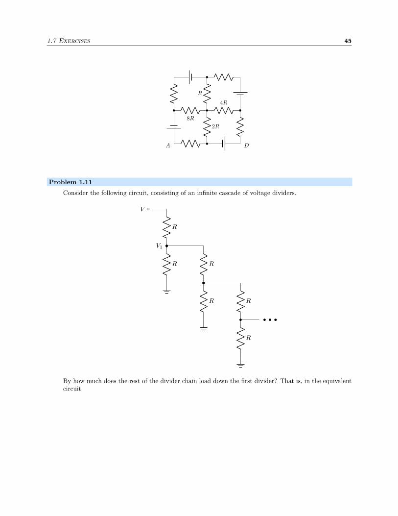
1.7 Exercises 45
R
2R
4R
8R
A D
Problem 1.11
Consider the following circuit, consisting of an infinite cascade of voltage dividers.
V
R
R R
R R
R
V1
By how much does the rest of the divider chain load down the first divider? That is, in the equivalentcircuit

46 Chapter 1. Resistors
V
R
Reff
V1
what is the value of Reff?
Hint: In the original divider chain, consider the second divider, along with the rest of the chain. This
part of the circuit is also equivalent to the same effective circuit. Now you have two different, equivalentcircuits in terms of R and Reff ; compute the resistance from the point V to ground in both circuits,equate, and solve for Reff .
Problem 1.12
Consider the circuit below, with 3 cascaded voltage dividers (not all the same).
V
R
R R/2
R R/2
R
Vout
(a) Compute Vout.
(b) Compute the current in each one of the resistors in the circuit, assuming no load connected to Vout.
Problem 1.13
Consider a network of 12 identical resistors of resistance R in the shape of a cube, as shown in thecircuit below. Compute the equivalent resistance between the two terminals shown at opposite cornersof the cube.

1.7 Exercises 47
R
R
R
R
R
R
R
RR
R
R
R
Hint: use symmetry, and analyze a current flowing between the two terminals. It also may (or maynot) help to identify which junctions are at equivalent potentials.
Problem 1.14
Consider the network below of 8 identical resistors and 4 identical voltage sources. With the twoindicated terminals as the output, give the Thévenin equivalent circuit. Explain your result.
V
R
V
R
V
R
V
RR
R
R
R
Problem 1.15
A “schmesistor” is a device that obeys “Schmohm’s law,”
V = I2S, (1.76)
where S is the “schmesistance.”
(a) Show that two schmesistors S1 and S2 in series behave like one schmesistor with schmesistanceSeff = S1 + S2.
(b) Show that two schmesistors S1 and S2 in parallel behave like one schmesistor with schmesistance
Seff =
(
1√S1
+1√S2
)−2
. (1.77)
(c) Describe the difficulty in using complex notation to analyze a circuit that includes schmesistors.
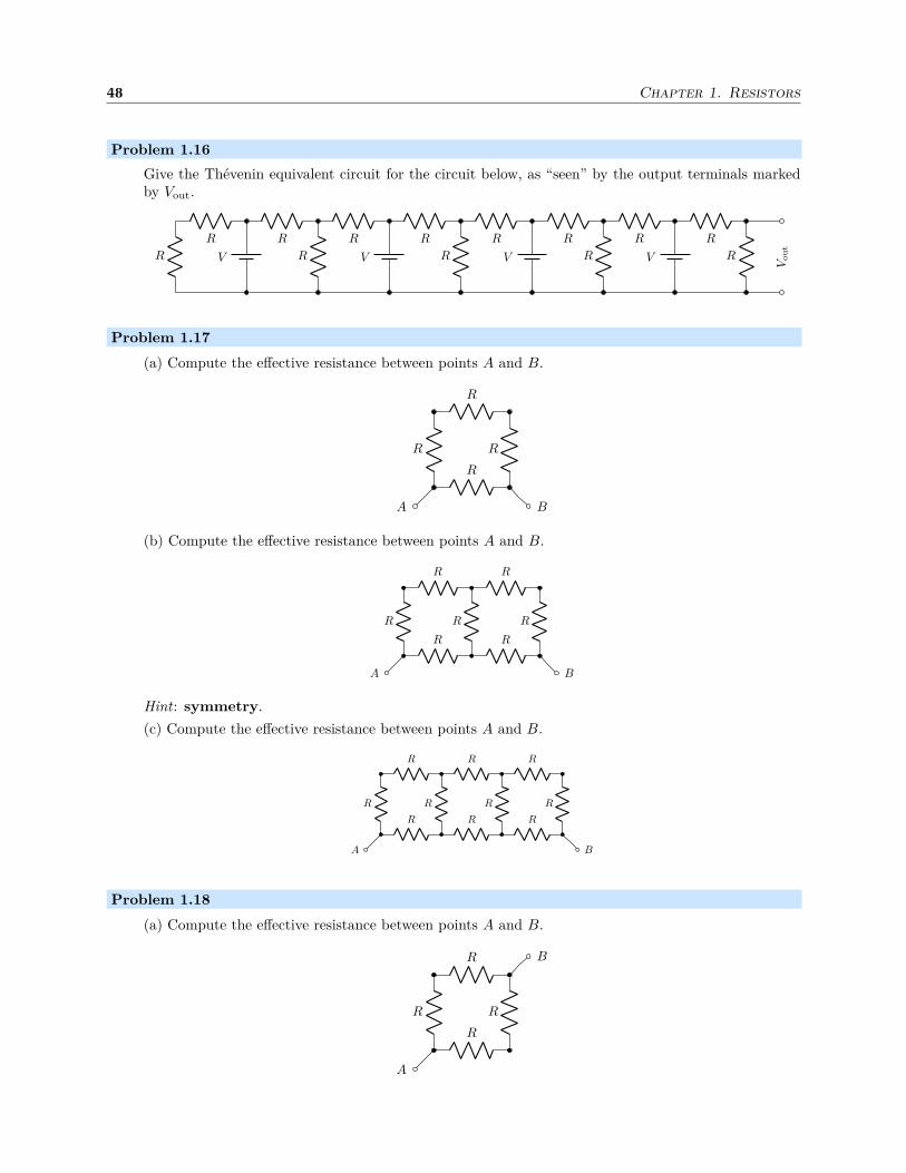
48 Chapter 1. Resistors
Problem 1.16
Give the Thévenin equivalent circuit for the circuit below, as “seen” by the output terminals markedby Vout.
Vo
ut
R
R
V
R
R
R
V
R
R
R
V
R
R
R
V
R
R
Problem 1.17
(a) Compute the effective resistance between points A and B.
R
R
R
R
A B
(b) Compute the effective resistance between points A and B.
R R R
R R
R R
A B
Hint: symmetry.
(c) Compute the effective resistance between points A and B.
R R R R
R R R
R R R
A B
Problem 1.18
(a) Compute the effective resistance between points A and B.
R
R
R
R
A
B
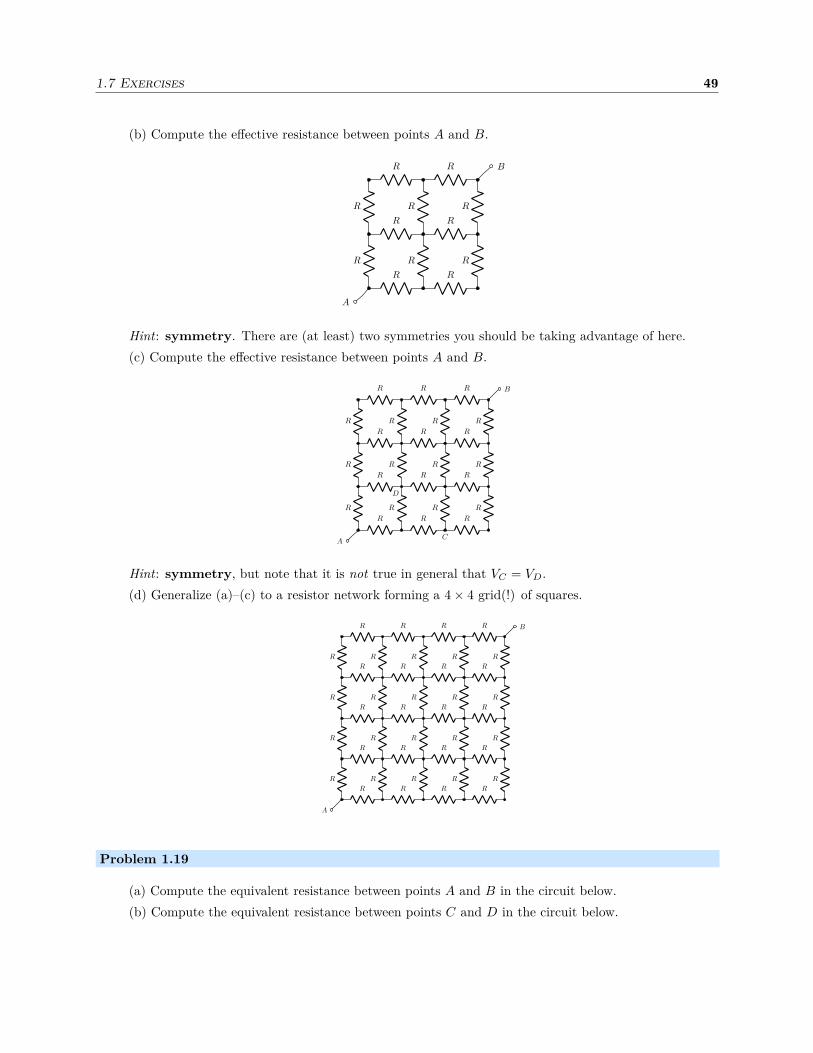
1.7 Exercises 49
(b) Compute the effective resistance between points A and B.
R
R
R
R
R
R
R R
R R
R R
A
B
Hint: symmetry. There are (at least) two symmetries you should be taking advantage of here.
(c) Compute the effective resistance between points A and B.
R
R
R
R
R
R
R
R
R
R
R
R
R R R
R R R
R R R
R R R
A
B
C
D
Hint: symmetry, but note that it is not true in general that VC = VD.
(d) Generalize (a)–(c) to a resistor network forming a 4× 4 grid(!) of squares.
R
R
R
R
R
R
R
R
R
R
R
R
R
R
R
R
R
R
R
R
R R R R
R R R R
R R R R
R R R R
R R R R
A
B
Problem 1.19
(a) Compute the equivalent resistance between points A and B in the circuit below.
(b) Compute the equivalent resistance between points C and D in the circuit below.

50 Chapter 1. Resistors
R
R
R
R
R R
R
R
R
R
R
R
R
R
R R R R
R
R R
R R R
R R R R
A
BC
D
Problem 1.20
Now back to the XKCD comic “Circuit Diagram.”5 The point of this problem is to apply the matrixmethod of Section 1.5 to solve this problem.
(a) Solve the example linear system in Eq. (1.39), using a computer, to obtain a value for V2, andthus for Reff . I will describe how you can do this in Mathematica as an example (which is obnoxiouslyexpensive but handy in that it will give exact results using this method), but a similar procedure willwork in some other software packages as well, such as the open-source Octave.6
First in a Mathematica window, type “A=”, and then under the menu Insert > Table/Matrix > New...,create a 4× 4 matrix. Then fill in the elements as above. Do the same thing to create a vector (4× 1matrix) for the currents (call it “II”, and use “IR” to represent IR in the vector; Mathematica reservesthe symbol “I” for
√−1). Finally, use LinearSolve[A, II] to obtain the solution vector v, and use
it to deduce the effective resistance.
(b) Modify the calculation to compute the effective resistance between nodes 3 and 4 in the sameexample circuit (reproduced below).
R
R
R
R
12
34
I
I
(c) Finally, modify the calculation to handle the XKCD mess.
The network is reproduced below, with nodes labeled (all 1-Ω resistors). You should set V11 = 0 andlet a current I flow into node 1 (and out node 11).
5http://xkcd.com/730/6http://octave.org

1.7 Exercises 51
12
34
5
6
7
89
10 11 12
1314


Chapter 2
Capacitors and Inductors
2.1 Capacitor Basics
A capacitor (an older, equivalent term is condensor) is, at minimum, a pair of conductors separated byvacuum or dielectric. The symbol itself depicts two parallel electrodes.
C
Generally, useful capacitors have a relatively large area to achieve a reasonably useful capacitance, so theyare something like a pair of planar conductors, with little separation. They may have stacks of many planarconductors to increase the area even further, and the stacks may be rolled up to save space and stored in acan or dipped in epoxy for robustness.
Capacitors act as devices to store charge, and in doing so they also store energy. The charge storedon the plates generates an electric field and thus a potential difference between the capacitor plates. Thepotential and charge are related by the capacitor law,
Q = CV,(2.1)
(capacitor law)
where C is the capacitance, measured in Farads (F), which characterizes the capacitor. Larger conductorareas, “stronger” dielectrics, and smaller electrode spacing all result in larger capacitance. (For example, afew twists to intertwine two pieces of insulated hookup wire makes a capacitor of a few pF.) Differentiatingthis relation at constant capacitance, and using I = dQ/dt, we find
I = CdV
dt,
(2.2)(capacitor charging)
which means that a current charges or discharges a capacitor, allowing it to build up or bleed off charge,thus changing the voltage.
There are many types of capacitors, and usually the different types are named according to theirdielectrics. A few of the most important are:
1. ceramic/monolithic: these tend to be cheap, and work reasonably well at high frequencies. Thecapacitances are fairly small in the overall spectrum, ranging from a ∼pF to about ∼0.1 µF.
2. electrolytic: generally this refers to aluminum electrolytic capacitors. In these capacitors, oneelectrode is aluminum foil, and the other is a liquid electrolyte. Under normal operation, an oxidelayer grows on the aluminum and acts as a thin dielectric layer. The foil can be coiled to give largesurface area, and the dielectric is very thin, so capacitances can be large, from ∼1 µF to ∼1 F or more,

54 Chapter 2. Capacitors and Inductors
though these tend not to work as well at high frequencies. These are polarized, meaning they canonly sustain voltage applied in one direction; the wrong voltage polarity can cause the insulating layerto break down, leading to failure of the capacitor.
3. tantalum: these are also electrolytic capacitors, with a sintered titanium pellet as one electrode, anda solid electrolyte as the other. These typically have intermediate capacitances in the range of ∼0.1 µFto ∼10 µF, and are fairly compact compared to aluminum electrolytics.
There are many other kinds of capacitors. Some examples include paper, mica, mylar, polystyrene, polypropy-lene, oil, and niobium electrolytic.
Like resistors, networked capacitors can combine to form equivalent single capacitors. Two capacitorsin parallel simply add their capacitances,
C1
C2 =
Ceff = C1 + C2
as resistors in series add. Two series capacitors add less straightforwardly,
C1 C2
=
C −1eff = C −1
1 + C −12
like two parallel resistors add.
2.2 Simple R–C Circuits
2.2.1 Integrator
Consider the simple R–C circuit below. It looks something like a voltage divider, with the lower resistorreplaced by a capacitor.
I
Vin
R
C
Vout
To analyze this (unloaded) circuit, note that all of the current I going through the resistor must also passthrough the capacitor. Applying Ohm’s law to determine the current,
Vin − Vout = IR, (2.3)
and then using the capacitor-charging law (2.2) to relate the current to the output voltage,
I = CdVout
dt. (2.4)
Solving for dVout/dt and eliminating I,
dVout(t)
dt= −Vout(t)
RC+
Vin(t)
RC.
(2.5)(differential equation for integrator)
Note that by comparing left- and right-hand sides here, we can see that RC must have the units of time forthe units to work out.
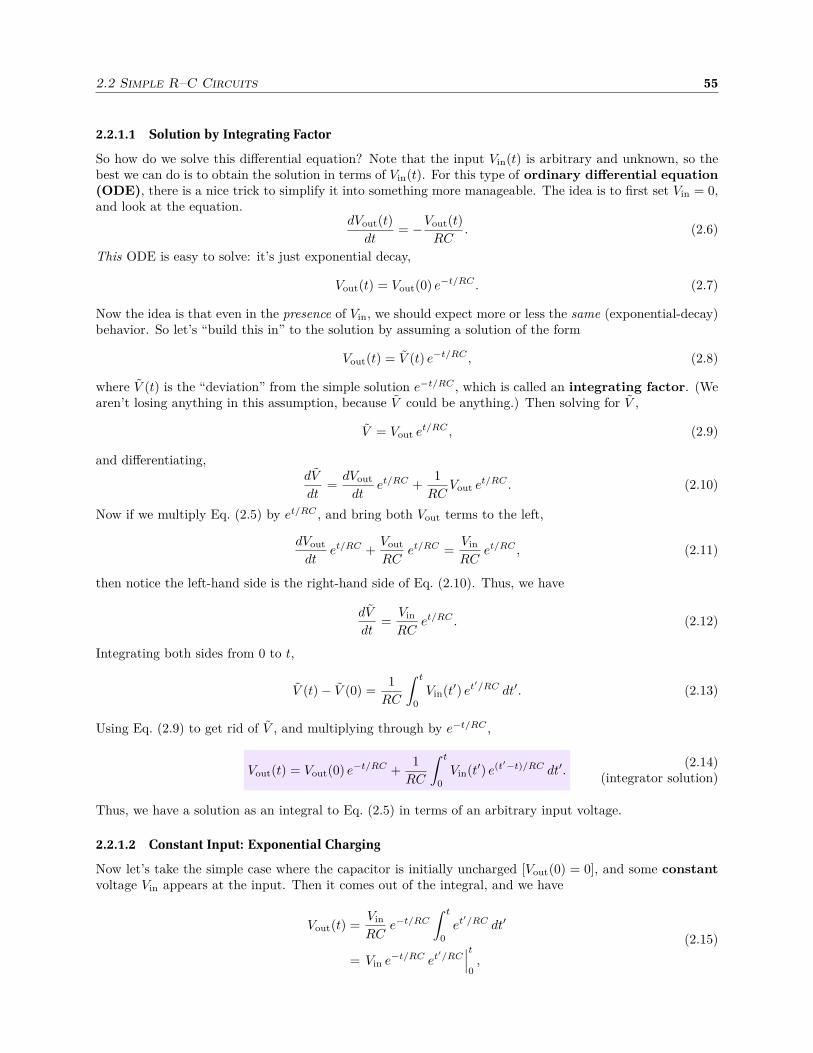
2.2 Simple R–C Circuits 55
2.2.1.1 Solution by Integrating Factor
So how do we solve this differential equation? Note that the input Vin(t) is arbitrary and unknown, so thebest we can do is to obtain the solution in terms of Vin(t). For this type of ordinary differential equation(ODE), there is a nice trick to simplify it into something more manageable. The idea is to first set Vin = 0,and look at the equation.
dVout(t)
dt= −Vout(t)
RC. (2.6)
This ODE is easy to solve: it’s just exponential decay,
Vout(t) = Vout(0) e−t/RC . (2.7)
Now the idea is that even in the presence of Vin, we should expect more or less the same (exponential-decay)behavior. So let’s “build this in” to the solution by assuming a solution of the form
Vout(t) = V (t) e−t/RC , (2.8)
where V (t) is the “deviation” from the simple solution e−t/RC , which is called an integrating factor. (Wearen’t losing anything in this assumption, because V could be anything.) Then solving for V ,
V = Vout et/RC , (2.9)
and differentiating,dV
dt=
dVout
dtet/RC +
1
RCVout et/RC . (2.10)
Now if we multiply Eq. (2.5) by et/RC , and bring both Vout terms to the left,
dVout
dtet/RC +
Vout
RCet/RC =
Vin
RCet/RC , (2.11)
then notice the left-hand side is the right-hand side of Eq. (2.10). Thus, we have
dV
dt=
Vin
RCet/RC . (2.12)
Integrating both sides from 0 to t,
V (t)− V (0) =1
RC
∫ t
0
Vin(t′) et′/RC dt′. (2.13)
Using Eq. (2.9) to get rid of V , and multiplying through by e−t/RC ,
Vout(t) = Vout(0) e−t/RC +1
RC
∫ t
0
Vin(t′) e(t′−t)/RC dt′.(2.14)
(integrator solution)
Thus, we have a solution as an integral to Eq. (2.5) in terms of an arbitrary input voltage.
2.2.1.2 Constant Input: Exponential Charging
Now let’s take the simple case where the capacitor is initially uncharged [Vout(0) = 0], and some constantvoltage Vin appears at the input. Then it comes out of the integral, and we have
Vout(t) =Vin
RCe−t/RC
∫ t
0
et′/RC dt′
= Vin e−t/RC et′/RC∣
∣
∣
t
0,
(2.15)

56 Chapter 2. Capacitors and Inductors
with final solution
Vout(t) = Vin
(
1− e−t/RC)
.(2.16)
(integrator solution, constant input)
This is an exponential rise from 0 to Vin, with time constant RC. That is, looking at e−t/RC when t = RC,this falls from unity to 1/e, or about 37%. So 1− e−t/RC , when t = RC, rises from 0 to 1 − 1/e, or about63%.
One important thing to note about this is that the capacitor tends to smooth the input. Here, wecan regard the problem as an input of a sudden voltage step at t = 0 [which is consistent with Vout(0) = 0],and the output is now smoothed over a time scale RC due to the exponential action of the R–C circuit.
2.2.1.3 Integration
This R–C circuit is called a passive integrator or integrator. The reason is as follows. Going back toEq. (2.5), if Vout ≪ Vin, then we can ignore the Vout term:
dVout(t)
dt≈ Vin(t)
RC. (2.17)
In this case, we can just integrate this equation directly from 0 to t:
Vout(t)− Vout(0) ≈ 1
RC
∫ t
0
Vin(t′) dt′. (2.18)
Thus, the output is the simple integral of the input signal, up to an offset and a factor of 1/RC. In thisregime, the capacitor simply stores up the charge that comes in from the resistor. If the capacitor charge,and hence voltage, becomes too large, then this reduces the voltage drop across the resistor, and the simpleintegral approximation breaks down.
2.2.2 Differentiator
We can get the other simple R–C circuit by interchanging the resistor and capacitor in the integrator, asshown below.
I
Vin
C
R
Vout
The capacitor charging equation here gives
I = Cd
dt
(
Vin − Vout
)
, (2.19)
while Ohm’s law gives
I =Vout
R. (2.20)
Eliminating I, we get
Vout
R= C
d
dt
(
Vin − Vout
)
.(2.21)
(differentiator ODE)

2.3 AC Signals and Complex Notation 57
which is the ODE for this circuit. This circuit is called a differentiator, for reasons analogous to what wesaw for the integrator. If Vout ≪ Vin, then the ODE reduces to
Vout
R≈ C
dVin
dt, (2.22)
and the output is approximately the derivative of the input.It is possible to write down a general solution to Eq. (2.21) for the differentiator output in terms of an
arbitrary input:
Vout(t) = Vin(t) +[
Vout(0)− Vin(0)]
e−t/RC − e−t/RC
RC
∫ t
0
Vin(t′) et′/RC dt′.
(differentiator solution) (2.23)The idea is fairly similar to the integrator (the same integrating-factor trick applies); we will leave this asan exercise.
2.3 AC Signals and Complex Notation
Suppose we have an ac signal (alternating-current signal), oscillating at a single frequency ω, described byvoltage:
V (t) = V0 cos ωt. (2.24)
Remember to distinguish angular frequencies from “regular frequencies.” Angular frequencies are usuallyrepresented by ω, and are measured in rad/s. “Regular” frequencies are usually represented by f or ν, andare measured in Hz or cycles/s. We can write
ω = 2πf(2.25)
(angular frequency)
to relate the two. In physics, using the angular frequency saves writing a bunch of factors of 2π, but whenquoting a physical value, it’s best to stick to regular frequencies. That, is you could quote an angularfrequency by saying “ω/2π = 100 Hz” instead of quoting the direct value of ω in rad/s.
As an example, let’s go back to the capacitor charging law,
I = CdV
dt. (2.26)
Then with the above ac signal, we have
I(t) = −ωCV0 sin ωt = ωCV0 cos(ωt + π/2), (2.27)
where in the last step, we changed the negative sine to a phase-shifted cosine. This makes the current easierto compare to the original voltage. In fact, we can see that the current leads the voltage in phase, becausethe current’s phase is larger by π/2 than the voltage’s phase. The shape of the current signal is otherwisethe same as the voltage, except for amplitude and phase.
2.3.1 Complex Phase
There is a nicer way to handle this monochromatic time dependence, and that is to introduce a complex-number notation. The idea is to represent the time dependence at frequency ω by a factor e−iωt.1 Thendefine a complex voltage
V = V0e−iωt. (2.28)
1Note that this is a common convention in physics; engineers usually use ejωt, where j = −i. The physics notation comesfrom the time dependence of a right-going plane wave, ei(kx−ωt).
58 Chapter 2. Capacitors and Inductors
The real (physical) voltage is just the real part of this, or
V (t) = Re[
V]
= Re[
V0e−iωt]
= V0 cos ωt, (2.29)
if V0 is real. The imaginary part, iV0 sin ωt, is “carried along” for mathematical convenience, and shouldbe dropped at the end of the calculation to get physical results. Thus, this works for linear circuits (in anonlinear circuit, a single frequency would be converted into other frequencies, so this analysis is best for acapacitor or resistor, but less so for a diode).
Why is this representation convenient? First, other phases are easy to represent as the phase of thecomplex coefficient V0. For example, we can write a phase φ as
V = V0e−iωt−iφ, (2.30)
and the real part of this isV (t) = V0 cos(ωt + φ), (2.31)
as we expect for this phase. However, if we absorb the phase φ into the complex voltage amplitude V0, thenV just looks like V0e−iωt.
The other nice thing about this complex notation is that derivatives, integrals, and their associatedphases are very easy to handle. We are assuming all time dependence is of the form e−iωt. Then a timederivative acts on the phase of any object like
d
dte−iωt−iφ =,−iωe−iωt−iφ. (2.32)
Since this always happens, we can formally identify
d
dt≡ −iω,
(2.33)(derivative for monochromatic signals)
provided we are discussing monochromatic signals. Then the capacitor-charging rule (2.26) becomes
I = −iωCV (2.34)
in complex notation.
2.3.2 Capacitive Reactance
We can interpret the complex form of the capacitor-charging rule in a powerful way. Solving for V , we find
V = Ii
ωC. (2.35)
In fact, this looks a lot like Ohm’s law, if we lump everything next to the I into an effective “resistance,”
XC :=i
ωC.
(2.36)(capacitive reactance)
This is called the capacitive reactance, and has the same units as resistance. It functions as somethinglike a resistance in the “Ohm’s law for capacitors,”
V = IXC ,(2.37)
(Ohm’s law for capacitors)
which is the same as Eqs. (2.35) and (2.26). However, because the reactance represents a derivative, itdepends on frequency. In fact, what this is saying is that capacitors have very high “resistance” at smallfrequencies (a capacitor is basically a broken wire, after all, and no current flows once the capacitor ischarged), but the capacitor acts like a short circuit at high frequencies, as we will see.
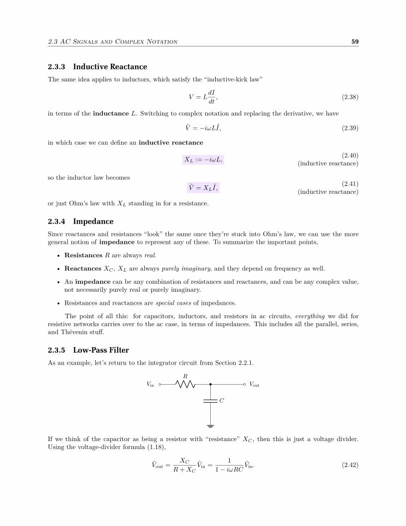
2.3 AC Signals and Complex Notation 59
2.3.3 Inductive Reactance
The same idea applies to inductors, which satisfy the “inductive-kick law”
V = LdI
dt, (2.38)
in terms of the inductance L. Switching to complex notation and replacing the derivative, we have
V = −iωLI, (2.39)
in which case we can define an inductive reactance
XL := −iωL,(2.40)
(inductive reactance)
so the inductor law becomes
V = XLI ,(2.41)
(inductive reactance)
or just Ohm’s law with XL standing in for a resistance.
2.3.4 Impedance
Since reactances and resistances “look” the same once they’re stuck into Ohm’s law, we can use the moregeneral notion of impedance to represent any of these. To summarize the important points,
• Resistances R are always real.
• Reactances XC , XL are always purely imaginary, and they depend on frequency as well.
• An impedance can be any combination of resistances and reactances, and can be any complex value,not necessarily purely real or purely imaginary.
• Resistances and reactances are special cases of impedances.
The point of all this: for capacitors, inductors, and resistors in ac circuits, everything we did forresistive networks carries over to the ac case, in terms of impedances. This includes all the parallel, series,and Thévenin stuff.
2.3.5 Low-Pass Filter
As an example, let’s return to the integrator circuit from Section 2.2.1.
Vin
R
C
Vout
If we think of the capacitor as being a resistor with “resistance” XC , then this is just a voltage divider.Using the voltage-divider formula (1.18),
Vout =XC
R + XCVin =
1
1− iωRCVin. (2.42)

60 Chapter 2. Capacitors and Inductors
This is a linear relation between the input and output voltage amplitudes, so to simplify the discussion abit, let’s define the transfer function
T (ω) :=Vout
Vin
,(2.43)
(transfer function)
which for the low-pass filter is
T (ω) =1
1− iωRC
(2.44)(transfer function)
from Eq. (2.42). To simplify even more, we can also consider the amplitude transfer function, whichdiscards the phase information:
T (ω) :=
∣
∣
∣
∣
Vout
Vin
∣
∣
∣
∣
.(2.45)
(amplitude transfer function)
Then for the low-pass filter, from Eq. (2.42) we have
T (ω) =1
√
1 + (ωRC)2.
(amplitude transfer function, low-pass filter) (2.46)Looking at the asymptotics of the low-pass filter, note that
• As ω −→ 0 (ω ≪ 1/RC), note that T (ω) −→ 1, which means that the integrator does not change thesignal at low frequencies.
• For large ω (ω ≫ 1/RC), T (ω) ∼ i/ωRC. Note that i = eiπ/2, and so ie−iωt = e−i(ωt−π/2). Thismeans the output phase lags the input phase by 90. Also, the output amplitude is reduced by afactor ω−1. This power-law behavior appears as a straight line on a log–log plot, with slope −1.
• The high-frequency scaling of ω−1 is usually called −6 dB/octave. Remember that decibels aredefined such that the ratio of two powers in decibels is of the form 10 log10(P/P0), and the ratioof two amplitudes is 20 log10(V/V0). One octave means a doubling of frequency (from the musicalterm), and ω−1 scaling means that doubling the frequency cuts the amplitude in half. In dB, this is20 log10(1/2) = −6 dB.
• The transition point between the low- and high-frequency behavior is called the 3-dB point, ormore properly, the −3-dB point. The convention is to define the transition point as the point whereT (ω) drops from 1 to 1/
√2 (so that the power transferred drops to 1/2). Then 20 log(1/
√2) = −3 dB.
We can find the corresponding frequency by setting T (ω3 dB) = 1/√
2, which has the solution
ω3 dB =1
RC, f3 dB =
1
2πRC.
(2.47)(3-dB frequency)
All this is summarized in the plot below.
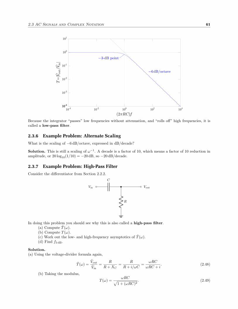
2.3 AC Signals and Complex Notation 61
(2pRC)f10-4 10410-2 100 102
To=
o|Vouto/
Vin
o|
101
10-4
100
10-1
10-2
10-3
10-4
-6odB/octave
-3-dB point
Because the integrator “passes” low frequencies without attenuation, and “rolls off” high frequencies, it iscalled a low-pass filter.
2.3.6 Example Problem: Alternate Scaling
What is the scaling of −6 dB/octave, expressed in dB/decade?
Solution. This is still a scaling of ω−1. A decade is a factor of 10, which means a factor of 10 reduction inamplitude, or 20 log10(1/10) = −20 dB, so −20 dB/decade.
2.3.7 Example Problem: High-Pass Filter
Consider the differentiator from Section 2.2.2.
Vin
C
R
Vout
In doing this problem you should see why this is also called a high-pass filter.(a) Compute T (ω).(b) Compute T (ω).(c) Work out the low- and high-frequency asymptotics of T (ω).(d) Find f3 dB.
Solution.(a) Using the voltage-divider formula again,
T (ω) =Vout
Vin
=R
R + XC=
R
R + i/ωC=
ωRC
ωRC + i. (2.48)
(b) Taking the modulus,
T (ω) =ωRC
√
1 + (ωRC)2. (2.49)
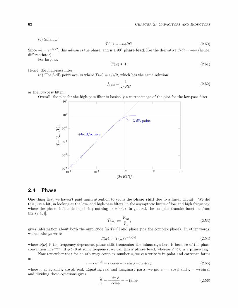
62 Chapter 2. Capacitors and Inductors
(c) Small ω:T (ω) ∼ −iωRC. (2.50)
Since −i = e−iπ/2, this advances the phase, and is a 90 phase lead, like the derivative d/dt = −iω (hence,differentiator).
For large ω:T (ω) ≈ 1. (2.51)
Hence, the high-pass filter.(d) The 3-dB point occurs where T (ω) = 1/
√2, which has the same solution
f3 dB =1
2πRC(2.52)
as the low-pass filter.Overall, the plot for the high-pass filter is basically a mirror image of the plot for the low-pass filter.
(2pRC)f10-4 10410-2 100 102
To=
o|Vou
to/V
ino|
101
10-4
100
10-1
10-2
10-3
10-4
+6odB/octave
-3-dB point
2.4 Phase
One thing that we haven’t paid much attention to yet is the phase shift due to a linear circuit. (We didthis just a bit, in looking at the low- and high-pass filters, in the asymptotic limits of low and high frequency,where the phase shift ended up being nothing or ±90.) In general, the complex transfer function [fromEq. (2.43)],
T (ω) :=Vout
Vin
, (2.53)
gives information about both the amplitude [in T (ω)] and phase (via the complex phase). In other words,we can always write
T (ω) := T (ω) e−iφ(ω), (2.54)
where φ(ω) is the frequency-dependent phase shift (remember the minus sign here is because of the phaseconvention in e−iωt. If φ > 0 at some frequency, we call this a phase lead, whereas φ < 0 is a phase lag.
Now remember that for an arbitrary complex number z, we can write it in polar and cartesian formsas
z = r e−iφ = r cos φ− ir sin φ =: x + iy, (2.55)
where r, φ, x, and y are all real. Equating real and imaginary parts, we get x = r cos φ and y = −r sin φ,and dividing these equations gives
y
x= − sin φ
cos φ= − tan φ. (2.56)

2.4 Phase 63
Solving for φ gives
φ = − tan−1 y
x, (2.57)
remembering that tan x is an odd function. Now x and y are respectively the real and imaginary parts ofT (ω), so
φ(ω) = − tan−1
(
Im[T (ω)]
Re[T (ω)]
)
.(2.58)
(phase shift of linear circuit)
Thus, we have the phase shift at any frequency in terms of the complex transfer function.
2.4.1 Example: Low-Pass Filter
In the low-pass filter, we had from Eq. (2.44)
T (ω) =1
1− iωRC. (2.59)
Multiplying upstairs and downstairs by 1 + iωRC, we can rewrite this as
T (ω) =1 + iωRC
1 + (ωRC)2. (2.60)
Now the real and imaginary parts are more obvious, and if we put these into Eq. (2.58), we get
φ(ω) = − tan−1(ωRC).(2.61)
(phase shift, low-pass filter)
How does this behave? In the extreme limits:
• For small frequencies [ω ≪ (RC)−1], φ ≈ −ωRC, which is a small (close to 0) phase lag.
• For large frequencies [ω ≫ (RC)−1], φ ≈ −π/2, which is a 90 phase lag.
In between, the phase lag moves smoothly between 0 and 90, as shown in the plot below.
(2pRC)f10-4 10410-2 100 102
f (
deg
rees
)
0
-90
-45
The high-pass filter is very similar, but the phase is 90 for small frequencies (in the “stop band”), andchanges to 0 for large frequencies (in the “pass band”).
64 Chapter 2. Capacitors and Inductors
2.5 Power
Now we arrive at the real meaning of why capacitors and inductors seem a lot like resistors, but with“imaginary resistance.” Remember that the power dissipated in a circuit is P = IV . This is still true in anac circuit, but
P (t) = I(t) V (t) (2.62)
is the instantaneous power. This can either be positive or negative; positive means dissipating energy orperhaps storing energy in a capacitor or inductor, while negative means we are getting some stored energyback.
What we’re interested in here is the time-averaged behavior, so we know the net effect of everythingthat happens over a cycle. So let’s assume a monochromatic voltage and a current, with a possible phaseshift φ in the current. In real notation, we have
V (t) = V0(cos ωt)
I(t) = I0 cos(ωt + φ).(2.63)
Then the power, time-averaged over one period T = 2π/ω is
〈P 〉 =1
T
∫ T
0
V (t) I(t) dt. (2.64)
Expanding the cosine in the current using the sum-angle formula,
I(t) = I0[cos(ωt) cos(φ)− sin(ωt) sin(φ)] (2.65)
and using this with the above expression for V (t), we get
〈P 〉 =I0V0
T
∫ T
0
[cos2(ωt) cos(φ)− cos(ωt) sin(ωt) sin(φ)] dt. (2.66)
In the second term the cos(ωt) sin(ωt) = (1/2) sin(2ωt) averages to zero. In the first term cos2(ωt) =(1/2) + (1/2) cos(2ωt), which averages to just 1/2. Thus,
〈P 〉 =1
2I0V0 cos(φ). (2.67)
Now to simplify this a bit more, we want to compare this to time-averaged values of V (t) and I(t) separately.It doesn’t make sense to time average them directly, because they average to zero. But we can compute therms or root-mean-square values. This just means: square it, time-average it, take the square root, done.For the voltage, if we square it,
V 2(t) = V 20 cos2 ωt, (2.68)
then average it,1
T
∫ T
0
V 2(t) dt =V 2
0
2, (2.69)
then take the square root, we get the rms voltage:
Vrms =V0√
2.
(2.70)(rms voltage)
Similarly, for current,
Irms =I0√
2.
(2.71)(rms current)

2.6 Resonant Circuits 65
Note that these two rms expressions are valid only for sine waves. Then we can rewrite Eq. (2.67) as
〈P 〉 = IrmsVrms cos(φ).(2.72)
(rms current)
It is common to define the power factor as
power factor :=〈P 〉
IrmsVrms= cos(φ).
(2.73)(power factor)
What does this mean? Breaking this down into cases:
• cos φ = 1 (φ = 0): this occurs for a purely resistive load; the maximum power is dissipated here.
• cos φ = 0 (|φ| = π/2): this is a purely reactive (capacitive or inductive) load, no power is dissipated (itis only stored and retrieved over each cycle).
• 0 < cos φ < 1 (0 < |φ| < π/2): there is some reactive component to the load impedance, so some poweris dissipated, but not as much as for an equivalently large but real impedance.
• cos φ < 0 (|φ| > π/2): it’s also possible to have a negative power factor, which means the “load” is infact a generator or EMF source.
Light bulbs and toasters are good examples of resistive loads. An example of a capacitive load is a piezospeaker or buzzer. Examples of inductive (reactive) loads are electric motors or lighting transformers orballasts for fluorescent lights (the “magnetic” kind, not the “electronic” kind). Inductive loads are importantin high-power applications, and the problem is that the power factor can be very small, so that large voltagesand currents are needed to drive a motor. This isn’t efficient, because the large voltages and currents causewasted power to be dissipated elsewhere. A trick to help here is to “correct” the phase of the load impedanceby connecting a parallel capacitor, which increases the power factor. It is common in air-conditioningcompressor motors to have two capacitors, a “start” capacitor and a “run” capacitor. The start capacitorincreases the parallel capacitance and hence the power factor when the motor first powers on, to give themotor extra startup torque.
2.6 Resonant Circuits
As another example of mixed impedances, we can consider a resonant filter with a resistor, inductor, andcapacitor, as shown below.
Vin
LC
R
Vout
Resonant LC circuits like this are also often called tank circuits. To analyze this, let’s lump the seriesinductor and capacitor together into a single element, of impedance
ZLC = XL + XC = −iωL +i
ωC
= − iL
ω
(
ω2 +1
LC
)
= − iL
ω
(
ω2 − ω 20
)
,
(2.74)

66 Chapter 2. Capacitors and Inductors
where we have defined the resonant (LC) frequency
ω0 :=1√LC
.(2.75)
(LC frequency)
Then we can treat what is left as a voltage divider. The transfer function is
T (ω) =R
R + ZLC
=R
R− (iL/ω)(ω2 − ω 20 )
=iωR/L
(ω2 − ω 20 ) + iωR/L
.
(2.76)
Defining the damping constant
γ :=R
L, (2.77)
the transfer function becomes
T (ω) =iωγ
(ω2 − ω 20 ) + iωγ
.(2.78)
(transfer function, RLC circuit)
This is the same as the response function for a damped harmonic oscillator, with resonant frequency ω0 anddamping rate γ.
T (ω) =ωγ
√
(ω2 − ω 20 )2 + ω2γ2
.
(amplitude transfer function, RLC circuit) (2.79)Note that on resonance (ω = ω0), T (ω = ω0) = 1 [and in fact T (ω = ω0) = 1, so the signal is transmittedwithout amplitude reduction or any phase shift. Away from resonance, T (ω) < 1, leading to a transmission“peak” around ω0.
2.6.1 Q Factor
A common way to quantify the width of the resonance peak is the Q factor. The idea is to find the −3 dBpoints of the resonance peaks (compared to the peak) as a measure of the width. Thus, setting T (ω) = 1/
√2,
1√2
=ωγ
√
(ω2 − ω 20 )2 + ω2γ2
, (2.80)
we can square this and rearrange to find
(ω2 − ω 20 )2 = ω2γ2. (2.81)
This is the square of a quadratic equations, with four solutions
ω = ±√
(γ/2)2 + ω20 ±
γ
2. (2.82)
We only want the positive solutions, because T (ω) ≥ 0, and T (ω) has the same sign as ω. Thus,
ω3dB =√
(γ/2)2 + ω20 ±
γ
2. (2.83)
If we define the width of the peak to be the difference between the −3-dB points,
δω3dB = γ.(2.84)
(full width at half maximum)
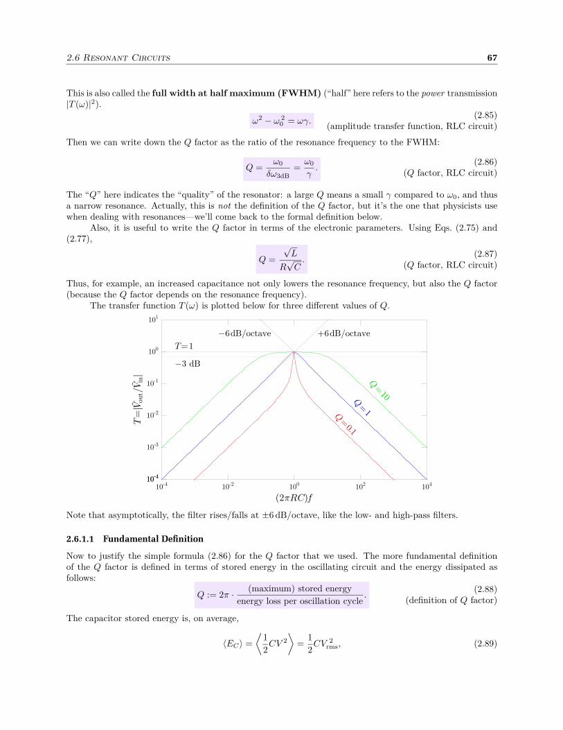
2.6 Resonant Circuits 67
This is also called the full width at half maximum (FWHM) (“half” here refers to the power transmission|T (ω)|2).
ω2 − ω 20 = ωγ.
(2.85)(amplitude transfer function, RLC circuit)
Then we can write down the Q factor as the ratio of the resonance frequency to the FWHM:
Q =ω0
δω3dB=
ω0
γ.
(2.86)(Q factor, RLC circuit)
The “Q” here indicates the “quality” of the resonator: a large Q means a small γ compared to ω0, and thusa narrow resonance. Actually, this is not the definition of the Q factor, but it’s the one that physicists usewhen dealing with resonances—we’ll come back to the formal definition below.
Also, it is useful to write the Q factor in terms of the electronic parameters. Using Eqs. (2.75) and(2.77),
Q =
√L
R√
C.
(2.87)(Q factor, RLC circuit)
Thus, for example, an increased capacitance not only lowers the resonance frequency, but also the Q factor(because the Q factor depends on the resonance frequency).
The transfer function T (ω) is plotted below for three different values of Q.
(2pRC)f10-4 10410-2 100 102
To=
o|Vou
to/V
ino|
101
10-4
100
10-1
10-2
10-3
10-4
-6odB/octave +6odB/octave
Qo=
o1
Qo=
o10
Qo=
o0.1
-3 dB
To=o1
Note that asymptotically, the filter rises/falls at ±6 dB/octave, like the low- and high-pass filters.
2.6.1.1 Fundamental Definition
Now to justify the simple formula (2.86) for the Q factor that we used. The more fundamental definitionof the Q factor is defined in terms of stored energy in the oscillating circuit and the energy dissipated asfollows:
Q := 2π · (maximum) stored energy
energy loss per oscillation cycle.
(2.88)(definition of Q factor)
The capacitor stored energy is, on average,
〈EC〉 =
⟨
1
2CV 2
⟩
=1
2CV 2
rms, (2.89)
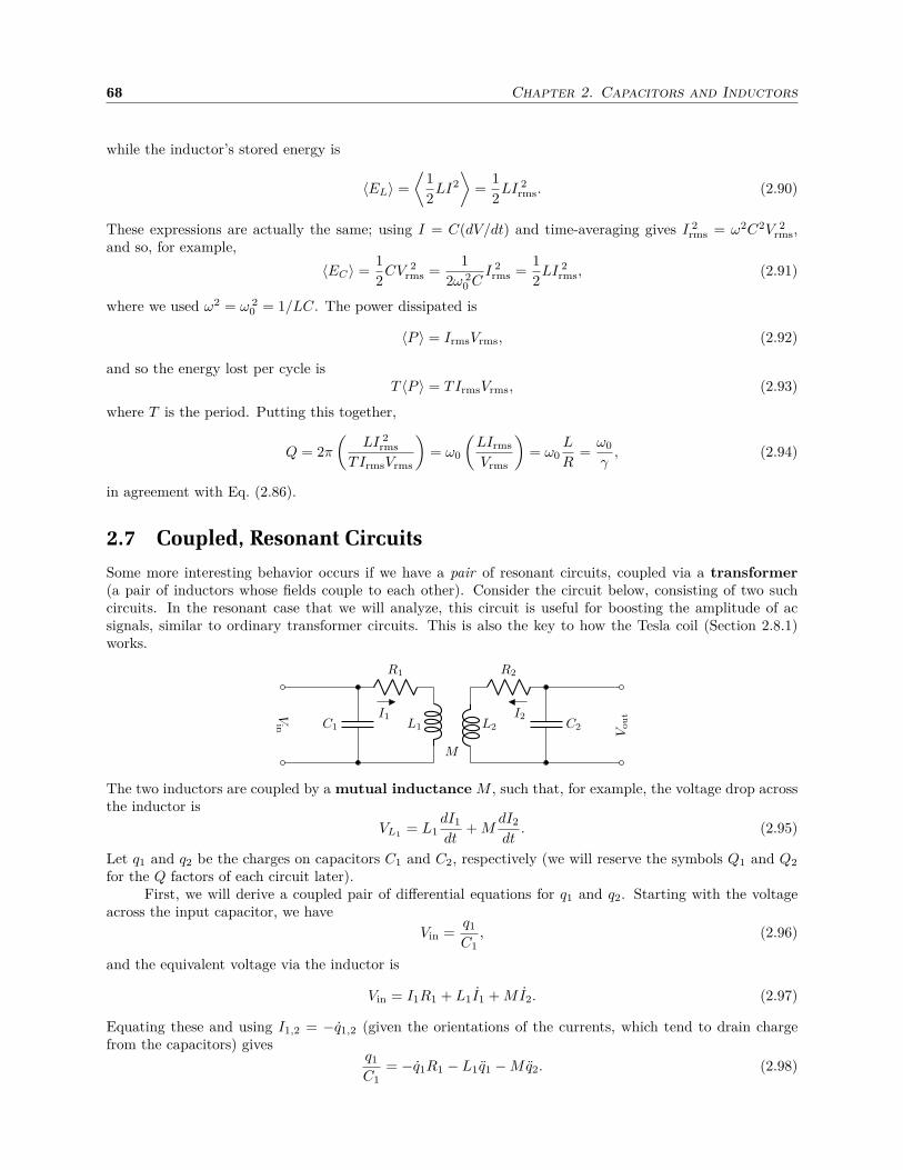
68 Chapter 2. Capacitors and Inductors
while the inductor’s stored energy is
〈EL〉 =
⟨
1
2LI2
⟩
=1
2LI 2
rms. (2.90)
These expressions are actually the same; using I = C(dV/dt) and time-averaging gives I 2rms = ω2C2V 2
rms,and so, for example,
〈EC〉 =1
2CV 2
rms =1
2ω 20 C
I 2rms =
1
2LI 2
rms, (2.91)
where we used ω2 = ω 20 = 1/LC. The power dissipated is
〈P 〉 = IrmsVrms, (2.92)
and so the energy lost per cycle isT 〈P 〉 = TIrmsVrms, (2.93)
where T is the period. Putting this together,
Q = 2π
(
LI 2rms
TIrmsVrms
)
= ω0
(
LIrms
Vrms
)
= ω0L
R=
ω0
γ, (2.94)
in agreement with Eq. (2.86).
2.7 Coupled, Resonant Circuits
Some more interesting behavior occurs if we have a pair of resonant circuits, coupled via a transformer(a pair of inductors whose fields couple to each other). Consider the circuit below, consisting of two suchcircuits. In the resonant case that we will analyze, this circuit is useful for boosting the amplitude of acsignals, similar to ordinary transformer circuits. This is also the key to how the Tesla coil (Section 2.8.1)works.
L1C1
R1
Vin
M
L2
R2
C2
Vo
utI1 I2
The two inductors are coupled by a mutual inductance M , such that, for example, the voltage drop acrossthe inductor is
VL1= L1
dI1
dt+ M
dI2
dt. (2.95)
Let q1 and q2 be the charges on capacitors C1 and C2, respectively (we will reserve the symbols Q1 and Q2
for the Q factors of each circuit later).First, we will derive a coupled pair of differential equations for q1 and q2. Starting with the voltage
across the input capacitor, we have
Vin =q1
C1, (2.96)
and the equivalent voltage via the inductor is
Vin = I1R1 + L1I1 + MI2. (2.97)
Equating these and using I1,2 = −q1,2 (given the orientations of the currents, which tend to drain chargefrom the capacitors) gives
q1
C1= −q1R1 − L1q1 −Mq2. (2.98)
2.7 Coupled, Resonant Circuits 69
Then simplifying, we have
ω 21 q1 + γ1q1 + q1 +
M
L1q2 = 0
ω 22 q2 + γ2q2 + q2 +
M
L2q1 = 0,
(2.99)
where we have written the matching equation for the output circuit. Here, the resonant frequencies of thecircuits are
ω1,2 :=1
√
L1,2C1,2
, (2.100)
and the damping rates are
γ1,2 :=R1,2
L1,2. (2.101)
Considering a sinusoidal input signal at frequency ω, The differential equations (2.99) also apply to complexcharges q1,2(t), with time dependence of the form
q1,2(t) = q1,2 e−iωt. (2.102)
This convention allows us to eliminate the derivatives in the coupled ODEs. That is, in complex notation,we just replace every derivative by (−iω), so that
ω 21 q1 − iωγ1q1 − ω2q1 − ω2 M
L1q2 = 0
ω 22 q2 +−iωγ2q2 − ω2q2 − ω2 M
L2q1 = 0.
(2.103)
These equations become(
ω 21 − ω2 − iωγ1
)
q1 − ω2 M
L1q2 = 0
(
ω 22 − ω2 − iωγ2
)
q2 − ω2 M
L2q1 = 0.
(2.104)
after a bit of simplification. Note that in matrix form, we can rewrite these equations as
(
ω 21 − ω2 − iωγ1
)
−ω2(M/L1)
−ω2(M/L2)(
ω 22 − ω2 − iωγ2
)
[
q1
q2
]
= 0.(2.105)
(evolution equations)
For any matrix equation of the form[
A BC D
] [
x1
x2
]
= 0 (2.106)
to hold the determinant of the 2x2 matrix must vanish; i.e., AD −BC = 0. Thus, we must have
(ω 21 − ω2 − iωγ1)(ω 2
2 − ω2 − iωγ2) = ω4k2,(2.107)
(frequency condition)
where
k :=M√L1L2
(2.108)
is the coupling coefficient for the inductor pair (satisfying 0 ≤ k ≤ 1). This is a quartic equation in ω; thephysical solutions determine the oscillation frequencies of the coupled-oscillator system. For now, note thatin the limit of zero coupling k and zero damping γ1,2, the solutions to this equation are ω = ±ω0 (note thatthe frequencies will appear as positive/negative pairs; the interpretation is that only the positive solutionis physical). In the more general case, there will be two physical frequencies, and in general the system

70 Chapter 2. Capacitors and Inductors
will oscillate at both frequencies simultaneously—because this is a linear system, the general solution is asuperposition of the individual frequencies.
The general condition (2.107) is somewhat cumbersome to analyze in general, so we will simplify tothe ideal-resonator limit, where R1,2 = 0 (and thus γ1,2 = 0), for matched resonators (ω1 = ω2 =: ω0). Inthis case, Eq. (2.107) becomes
(ω 20 − ω2)2 = ω4k2. (2.109)
Again, this condition has four solutions, but the only two positive (and thus physical) frequencies are
ω± =ω0√1± k
. (2.110)
Now Eqs. (2.104) become(
ω 20 − ω 2
±
)
q1 = ω 2±
M
L1q2
(
ω 20 − ω 2
±
)
q2 = ω 2±
M
L2q1
(2.111)
at the permitted frequencies. Dividing these equations gives
∣
∣
∣
∣
q1
q2
∣
∣
∣
∣
=
√
L2
L1. (2.112)
Using q1,2 = C1,2V1,2, we then have a circuit voltage “gain” of
G :=
∣
∣
∣
∣
Vout
Vin
∣
∣
∣
∣
=q2C1
q1C2=
√L1C1√L2C2
=
√
C1
C2=
√
L2
L1.
(2.113)(resonant “gain”)
Here, we used L1C1 = L2C2, since the resonances are matched (ω1 = ω2). This shows that the coupledresonances have a large step-up effect in voltage if the inductance of the second coil is large. Recall that for anideal solenoid L ∝ N2, so that the gain appears to be just N2/N1, as we might expect for a transformer circuit.However, note that there are extra geometric factors involved that may differ between the two inductors thatobscure this interpretation. Note also that this solution is independent of the coupling coefficient k—a sideeffect of the coincident circuit resonances.
Besides the step-up, there is some dynamical behavior. Recall that the oscillation frequencies are ω±,and so the general solution is
q1(t) = Ae−iω+t + Be−iω−t, (2.114)
for example, for the part of the solution applyling to the first circuit. If we assume that q1(0) = q0 is real,then the coefficients are real and equal, and we can assume a real solution of the form
q1(t) =q0
2
(
cos ω+t + cos ω−t)
. (2.115)
Now to obtain a more precise version of Eq. (2.112), note that Eq. (2.110) may be written as ω2/ω 20 = 1±k,
and so the matrix equation (2.105) may be rewritten
[
±k −M/L1
−M/L2 ±k
] [
q1
q2
]
= 0, (2.116)
corresponding to frequencies ω±. This means that at frequency ω±, ±kq1 = (M/L1)q2, so
q2 = ±kL1
Mq1 = ±
√
L1
L2q1 = ±Gq1. (2.117)
Thus the solution for q2 corresponding to Eq. (2.115) is
q2(t) =q0G
2
(
cos ω+t− cos ω−t)
, (2.118)
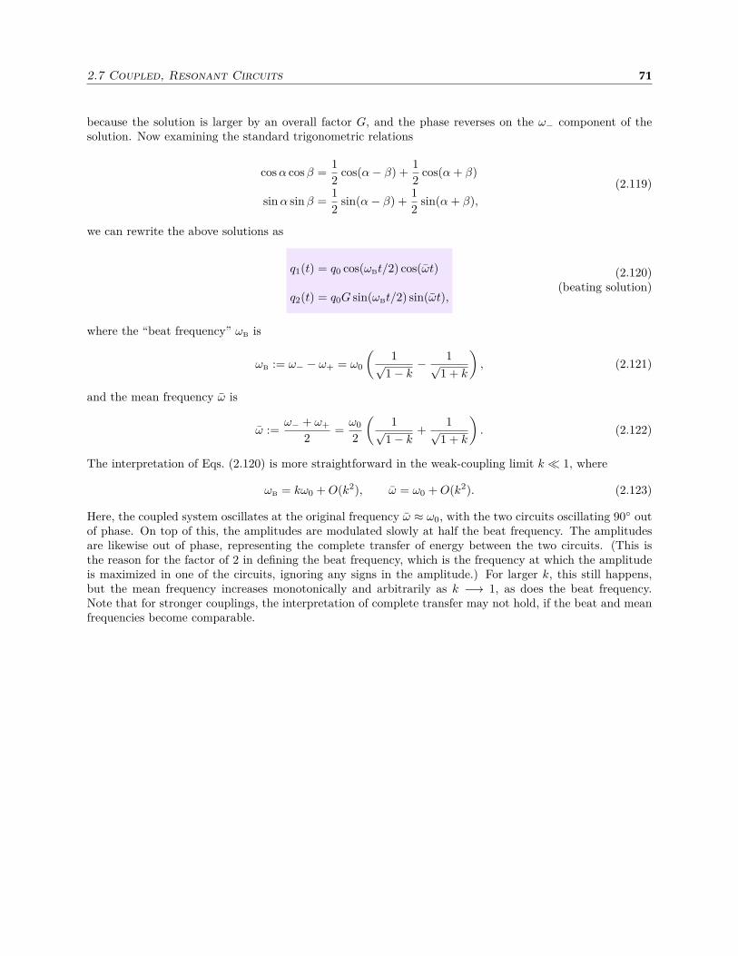
2.7 Coupled, Resonant Circuits 71
because the solution is larger by an overall factor G, and the phase reverses on the ω− component of thesolution. Now examining the standard trigonometric relations
cos α cos β =1
2cos(α− β) +
1
2cos(α + β)
sin α sin β =1
2sin(α− β) +
1
2sin(α + β),
(2.119)
we can rewrite the above solutions as
q1(t) = q0 cos(ωBt/2) cos(ωt)
q2(t) = q0G sin(ωBt/2) sin(ωt),
(2.120)(beating solution)
where the “beat frequency” ωB is
ωB := ω− − ω+ = ω0
(
1√1− k
− 1√1 + k
)
, (2.121)
and the mean frequency ω is
ω :=ω− + ω+
2=
ω0
2
(
1√1− k
+1√
1 + k
)
. (2.122)
The interpretation of Eqs. (2.120) is more straightforward in the weak-coupling limit k ≪ 1, where
ωB = kω0 + O(k2), ω = ω0 + O(k2). (2.123)
Here, the coupled system oscillates at the original frequency ω ≈ ω0, with the two circuits oscillating 90 outof phase. On top of this, the amplitudes are modulated slowly at half the beat frequency. The amplitudesare likewise out of phase, representing the complete transfer of energy between the two circuits. (This isthe reason for the factor of 2 in defining the beat frequency, which is the frequency at which the amplitudeis maximized in one of the circuits, ignoring any signs in the amplitude.) For larger k, this still happens,but the mean frequency increases monotonically and arbitrarily as k −→ 1, as does the beat frequency.Note that for stronger couplings, the interpretation of complete transfer may not hold, if the beat and meanfrequencies become comparable.
72 Chapter 2. Capacitors and Inductors
2.8 Circuit Practice
2.8.1 Tesla Coil
A nice example of a resonant circuit is the Tesla coil. There are many variations, but the simplest circuitis below. The idea is to put in a fairly “low” voltage (line voltage), and generate an output voltage as largeas possible, preferably at least hundreds of kV or even MV.
Here we will go through a basic tesla coil circuit to give you some experience in “reading” a morecomplex circuit diagram.
120 V ∼kV
spark gap
pri
mar
y
seco
ndar
y
Vout
Typical designs use a neon-sign transformer in the first stage to boost the voltage to ∼6 kV or more. Thisdrives an RLC circuit (the “R” is the wire resistance), which oscillates at a tunable resonant frequency (bytuning the variable inductor). A spark gap also interrupts the RLC circuit; the nonlinear sparking increasesdI/dt to help get a larger output voltage in the secondary transformer. The secondary coil is just a longair-core coil with many turns, with a large electrode on top. The capacitance of the secondary circuit is thecapacitance due to the windings of the coil, as well as the output terminal (the other electrode being ground).So the secondary circuit is also an RLC oscillator. The primary is tuned to resonate with the secondary. Theoscillators are generally tuned to radio frequencies (hundreds of kHz), which makes the output (relatively)safe for humans.
The coupled-oscillator analysis of Section 2.7 applies here, such that the voltage step-up factor canbe written as either
√
Cprimary/Csecondary or√
Lsecondary/Lprimary. Thus, for example, a large primarycapacitance leads to a large output voltage. A simple, heuristic derivation of this same result comes fromnoting that the maximum energy stored in the primary capacitor has the form E1 = (1/2)CprimaryV 2
1 . Ifwe assume all the energy is transferred to the secondary, then we can equate this to the analogous relationfor the secondary capacitance energy, obtaining that V2/V1 =
√
Cprimary/Csecondary. However, note thatthis circuit does not act as a simple transformer—for example, on resonance the secondary circuit acts as aquarter-wave antenna (so that the node of a standing wave occurs at ground, and an antinode occurs at theoutput terminal), so that the voltage and current are not constant through the secondary winding.

2.9 Exercises 73
2.9 Exercises
Problem 2.1
Use the capacitor law Q = CV to show that the effective capacitance of two parallel capacitors isCeff = C1 + C2, where C1 and C2 are the capacitances of the individual capacitors.
Problem 2.2
Show that the effective capacitance Ceff of two capacitors C1 and C2 in series is given by C −1eff =
C −11 + C −1
2 .
Problem 2.3
Consider the differentiator circuit shown below, where Vin(t) is an arbitrary input voltage.
C
Vin
R
Vout
(a) Show that the differential equation for this circuit is given by
dVout
dt= −Vout
RC+
dVin
dt. (2.124)
(We did this in class.)
(b) Use the integrating-factor trick that we used for the integrator circuit (i.e., define V := Voutet/RC ,
simplify the equation, and integrate from 0 to t) to find the general solution
Vout(t) = Vin(t) +[
Vout(0)− Vin(0)]
e−t/RC − e−t/RC
RC
∫ t
0
Vin(t′) et′/RC dt′. (2.125)
(c) Write down the solution in the case where Vin is turned on suddenly to a constant value from 0,just after t = 0. Give a brief, qualitative description of the solution (use a sketch if you need to).
Note: the reason for assuming the turn-on comes just after t = 0 is a bit technical, but it’s necessaryto get the boundary terms in the general solution to come out right. Basically, the “leading edge” ofthe input signal is an “interesting” part of the signal (the most interesting, actually), and so we mustmake sure to capture it in our interval of integration. Equivalently, we could have taken out integrationrange from −∞ to t, taking our boundary condition to be Vin(−∞) = 0.
Another note: From your solution here, you should see the reason why this circuit is called a “dc block.”
Problem 2.4
Consider the LR circuit below.
L
R
Vin(t) Vout(t)
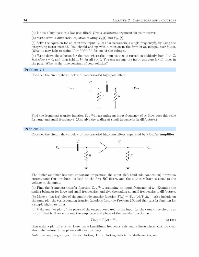
74 Chapter 2. Capacitors and Inductors
(a) Is this a high-pass or a low-pass filter? Give a qualitative argument for your answer.
(b) Write down a differential equation relating Vin(t) and Vout(t).
(c) Solve the equation for an arbitrary input Vin(t) (not necessarily a single frequency!), by using theintegrating-factor method. You should end up with a solution in the form of an integral over Vin(t).(Hint: it may help to define V := V e(R/L)t for one of the voltages.
(d) Write down the solution for the case where the input voltage is turned on suddenly from 0 to V0
just after t = 0, and then held at V0 for all t > 0. You can assume the input was zero for all times inthe past. What is the time constant of your solution?
Problem 2.5
Consider the circuit shown below of two cascaded high-pass filters.
Vin
C
R
C
R
Vout
Find the (complex) transfer function Vout/Vin, assuming an input frequency of ω. How does this scalefor large and small frequency? (Also give the scaling at small frequencies in dB/octave.)
Problem 2.6
Consider the circuit shown below of two cascaded high-pass filters, separated by a buffer amplifier.
Vin
C
R
C
R
Vout
The buffer amplifier has two important properties: the input (left-hand-side connection) draws nocurrent (and thus produces no load on the first RC filter), and the output voltage is equal to thevoltage at the input.
(a) Find the (complex) transfer function Vout/Vin, assuming an input frequency of ω. Examine thescaling behavior for large and small frequencies, and give the scaling at small frequencies in dB/octave.
(b) Make a (log-log) plot of the amplitude transfer function T (ω) = |Vout(ω)/Vin(ω)|. Also include onthe same plot the corresponding transfer functions from the Problem 2.5, and the transfer function fora simple high-pass filter.
(c) Make another plot of the phase of the output compared to the input for the same three circuits asin (b). That is, if we write out the amplitude and phase of the transfer function as
T (ω) = T (ω) e−iφ, (2.126)
then make a plot of φ vs. ω. Here, use a logarithmic frequency axis, and a linear phase axis. Be clearabout the nature of the phase shift (lead vs. lag).
Note: use any program you like for plotting. For a plotting tutorial in Mathematica, see
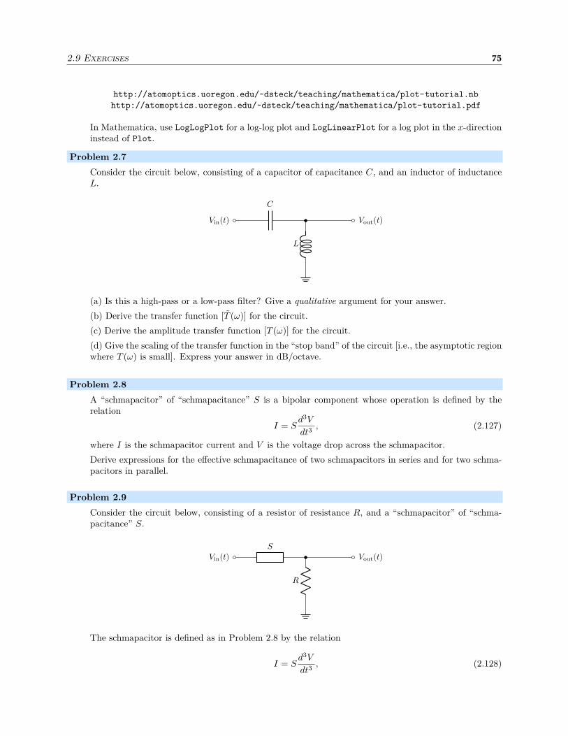
2.9 Exercises 75
http://atomoptics.uoregon.edu/~dsteck/teaching/mathematica/plot-tutorial.nb
http://atomoptics.uoregon.edu/~dsteck/teaching/mathematica/plot-tutorial.pdf
In Mathematica, use LogLogPlot for a log-log plot and LogLinearPlot for a log plot in the x-directioninstead of Plot.
Problem 2.7
Consider the circuit below, consisting of a capacitor of capacitance C, and an inductor of inductanceL.
C
L
Vin(t) Vout(t)
(a) Is this a high-pass or a low-pass filter? Give a qualitative argument for your answer.
(b) Derive the transfer function [T (ω)] for the circuit.
(c) Derive the amplitude transfer function [T (ω)] for the circuit.
(d) Give the scaling of the transfer function in the “stop band” of the circuit [i.e., the asymptotic regionwhere T (ω) is small]. Express your answer in dB/octave.
Problem 2.8
A “schmapacitor” of “schmapacitance” S is a bipolar component whose operation is defined by therelation
I = Sd3V
dt3, (2.127)
where I is the schmapacitor current and V is the voltage drop across the schmapacitor.
Derive expressions for the effective schmapacitance of two schmapacitors in series and for two schma-pacitors in parallel.
Problem 2.9
Consider the circuit below, consisting of a resistor of resistance R, and a “schmapacitor” of “schma-pacitance” S.
S
R
Vin(t) Vout(t)
The schmapacitor is defined as in Problem 2.8 by the relation
I = Sd3V
dt3, (2.128)

76 Chapter 2. Capacitors and Inductors
where I is the schmapacitor current and V is the voltage drop across the schmapacitor.
(a) Is this a high-pass or a low-pass filter? Give a qualitative argument for your answer.
(b) Derive the transfer function [T (ω)] for the circuit.
(c) Derive the amplitude transfer function [T (ω)] for the circuit.
(d) Give the scaling of the transfer function in the “stop band” of the circuit [i.e., the asymptotic regionwhere T (ω) is small]. Express your answer in dB/octave.
(e) What is the asymptotic phase in the stop band? Is it a phase lead or a phase lag?
(f) Derive an expression for the −3-dB frequency f3dB of the circuit.
Problem 2.10
Consider the RLC circuit below.
Vin(t)
C
LR
Vout(t)
(a) Derive the transfer function T (ω) for the circuit.
(b) Derive the amplitude transfer function [T (ω)] for the circuit.
(c) What is the behavior of T (ω) for small and large frequencies? What happens at ω = 1/√
LC? Basedon your answers, give a qualitative description of how this circuit functions as a frequency-dependentfilter.
Problem 2.11
A “schmesonator” is a bipolar component defined by the relation
V (t) = S1dI(t)
dt+ S2
∫ t
t0
I(t′) dt′, (2.129)
where S1 and S2 are constant parameters, and t0 is the time at which the schmesonator circuit is“schmactivated.”
Derive an expression for the schmesonative reactance (i.e., the impedance of the schmesonator assumingvoltage and current oscillate at frequency ω).

Chapter 3
Diodes
3.1 Ideal Diode
Diodes are useful circuit elements: in the simplest sense, they act as one-way valves or “trapdoors” forelectrons and thus for electrical current. Schematically, the following symbol represents them:
I−→anode cathode
The two terminals are called the anode and cathode. The rules that govern the ideal diode are as follows:
1. If Vanode > Vcathode, then the diode acts like a short circuit: lots of current can flow. In this case,the diode is said to be forward-biased.
2. If Vanode ≤ Vcathode, then the diode acts like an open circuit: no current flows at all. In this case,the diode is said to be reverse-biased.
Of course, the situation with real diodes is more complicated, and we’ll get to that. For now, a goodmnemonic to remember the direction of current flow is that the diode symbol makes an “arrow” in thedirection of the current flow (towards the cathode). Also, in the lab, a typical “signal diode” (for mA-levelcurrents) looks schematically like this:
anode cathode
There is usually a band (not always dark) that marks the cathode end; you can think of the band as beinga “minus sign” that marks the cathode.
The diode is obviously a nonlinear device, since voltage is not simply proportional to current. SinceOhm’s law V = IR does not hold in a simple way with constant R, so a diode is an example of a non-Ohmicdevice.
3.2 Vacuum Diodes
The name of the diode comes from the original vacuum-tube realization of a diode, which has two electrodes(hence, the “di”). The cathode is a heated electrode that “boils off” electrons; whether the electrons make itto the anode—and hence whether current flows—is determined by the relative voltage on the anode, becausethe anode with either repel or attract the electrons from the cathode. (Think about it to see that the currentflows only with the correct voltage polarity.)
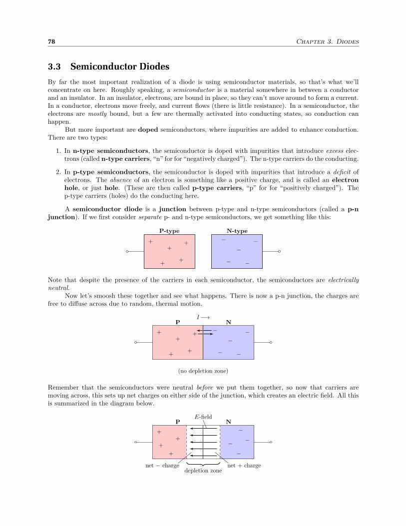
78 Chapter 3. Diodes
3.3 Semiconductor Diodes
By far the most important realization of a diode is using semiconductor materials, so that’s what we’llconcentrate on here. Roughly speaking, a semiconductor is a material somewhere in between a conductorand an insulator. In an insulator, electrons, are bound in place, so they can’t move around to form a current.In a conductor, electrons move freely, and current flows (there is little resistance). In a semiconductor, theelectrons are mostly bound, but a few are thermally activated into conducting states, so conduction canhappen.
But more important are doped semiconductors, where impurities are added to enhance conduction.There are two types:
1. In n-type semiconductors, the semiconductor is doped with impurities that introduce excess elec-trons (called n-type carriers, “n” for for “negatively charged”). The n-type carriers do the conducting.
2. In p-type semiconductors, the semiconductor is doped with impurities that introduce a deficit ofelectrons. The absence of an electron is something like a positive charge, and is called an electronhole, or just hole. (These are then called p-type carriers, “p” for for “positively charged”). Thep-type carriers (holes) do the conducting here.
A semiconductor diode is a junction between p-type and n-type semiconductors (called a p-njunction). If we first consider separate p- and n-type semiconductors, we get something like this:
P-type N-type
+
+
++
+
−
−
−−
−
Note that despite the presence of the carriers in each semiconductor, the semiconductors are electrically
neutral.Now let’s smoosh these together and see what happens. There is now a p-n junction, the charges are
free to diffuse across due to random, thermal motion.
(no depletion zone)
I−→P N
+
+
++
+
−
−
−−
−
Remember that the semiconductors were neutral before we put them together, so now that carriers aremoving across, this sets up net charges on either side of the junction, which creates an electric field. All thisis summarized in the diagram below.
depletion zone
E-field
net + chargenet − charge
P N
+
+
++ −
−
−
−
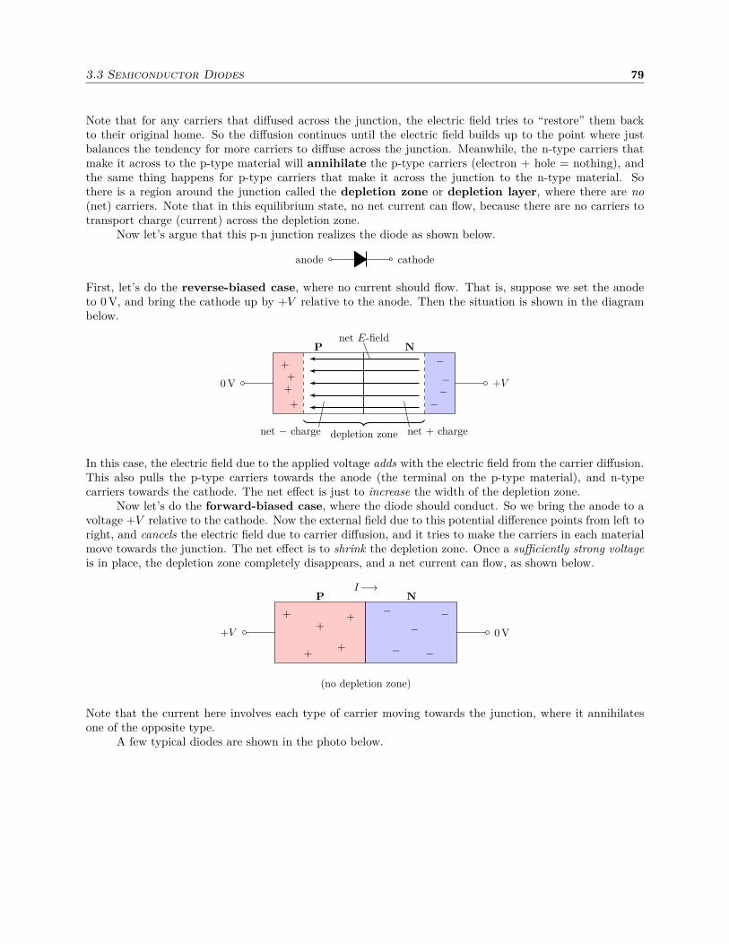
3.3 Semiconductor Diodes 79
Note that for any carriers that diffused across the junction, the electric field tries to “restore” them backto their original home. So the diffusion continues until the electric field builds up to the point where justbalances the tendency for more carriers to diffuse across the junction. Meanwhile, the n-type carriers thatmake it across to the p-type material will annihilate the p-type carriers (electron + hole = nothing), andthe same thing happens for p-type carriers that make it across the junction to the n-type material. Sothere is a region around the junction called the depletion zone or depletion layer, where there are no
(net) carriers. Note that in this equilibrium state, no net current can flow, because there are no carriers totransport charge (current) across the depletion zone.
Now let’s argue that this p-n junction realizes the diode as shown below.
anode cathode
First, let’s do the reverse-biased case, where no current should flow. That is, suppose we set the anodeto 0 V, and bring the cathode up by +V relative to the anode. Then the situation is shown in the diagrambelow.
depletion zone
net E-field
net + chargenet − charge
0 V
P
+V
N
+
+
++ −
−
−
−
In this case, the electric field due to the applied voltage adds with the electric field from the carrier diffusion.This also pulls the p-type carriers towards the anode (the terminal on the p-type material), and n-typecarriers towards the cathode. The net effect is just to increase the width of the depletion zone.
Now let’s do the forward-biased case, where the diode should conduct. So we bring the anode to avoltage +V relative to the cathode. Now the external field due to this potential difference points from left toright, and cancels the electric field due to carrier diffusion, and it tries to make the carriers in each materialmove towards the junction. The net effect is to shrink the depletion zone. Once a sufficiently strong voltage
is in place, the depletion zone completely disappears, and a net current can flow, as shown below.
(no depletion zone)
I−→
+V
P
0 V
N
+
+
++
+
−
−
−−
−
Note that the current here involves each type of carrier moving towards the junction, where it annihilatesone of the opposite type.
A few typical diodes are shown in the photo below.

80 Chapter 3. Diodes
From left to right, these are: 1N914B (signal diode), 1N4001 (1-A, general-purpose rectifier), MR752 (6-A,200-V rectifier), GI754 (6-A, 400-V rectifier). All cathodes point to the upper-right-hand corner.
3.4 Current–Voltage Characteristics
All these effects lead to a more complicated relation between voltage and current. Below is a schematic plotof the V –I relation for a diode.
I
V
reverse breakdown
reverse leakage
forward conduction
This is the forward current I plotted against the forward voltage V ; negative values of course indicate thatthe voltage/current are going in the reverse-biased direction. There are a few features to notice here.
1. Forward conduction. As the diode is forward-biased, the forward current rapidly (in fact, exponen-tially) increases. But for any forward current, there is a forward voltage drop—remember this isneeded to squish the depletion region down to nothing so the diode can conduct. A handy number toremember for quick calculations is 0.7 V for the voltage drop, for forward-biased silicon diodes. Thedrop is somewhat more for high-power diodes, somewhat less for Schottky and germanium diodes. Forexample, the common 1N914 (silicon signal diode) has a forward voltage drop of 0.7 V at 10 mA, drop-ping to 0.6 V at 1 mA and going up to 0.9 V at 100 mA. The 1N5711 Schottky diode (small-signal diode,rated for 15-mA maximum current) has a similar drop of about 0.7 V at 10 mA, but a comparativelylower drop of 0.4 V at 1 mA. These numbers are all temperature-dependent, but the values here are at25C, and vary from device to device.
2. Reverse leakage. When the diode is reverse-biased, the current is not completely blocked, but somecurrent flows. This is roughly constant over a wide range of reverse-bias voltages, and is usually labelled
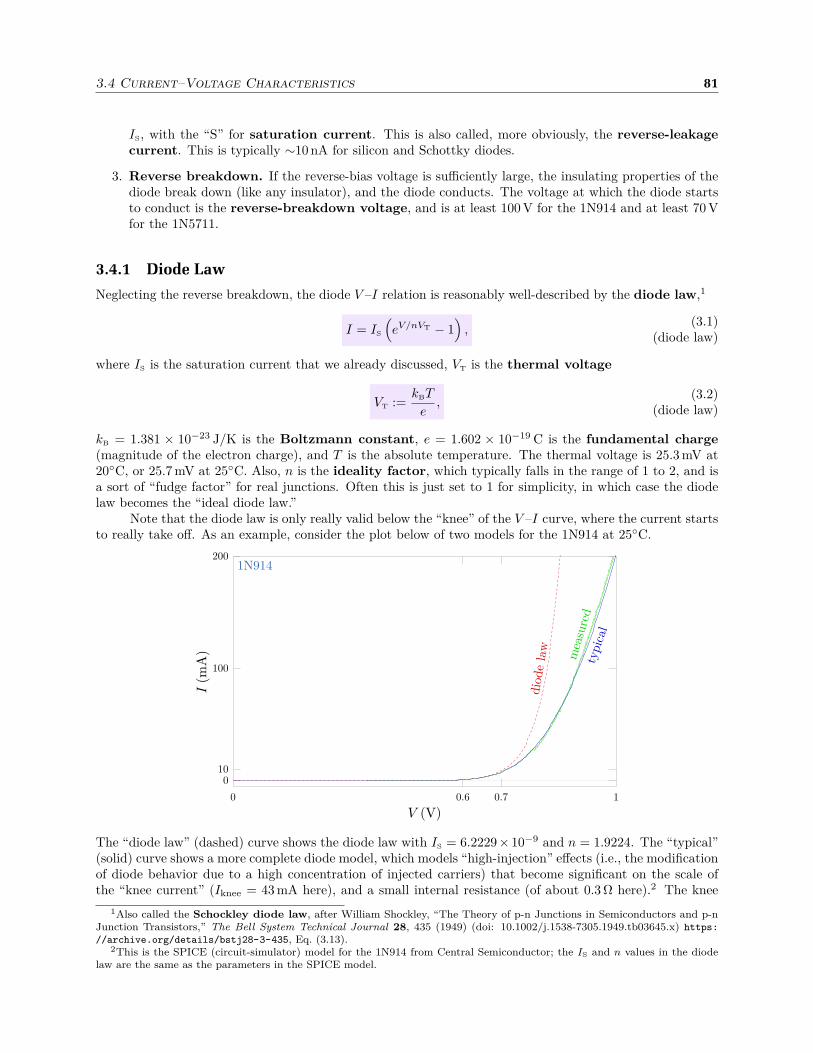
3.4 Current–Voltage Characteristics 81
IS, with the “S” for saturation current. This is also called, more obviously, the reverse-leakagecurrent. This is typically ∼10 nA for silicon and Schottky diodes.
3. Reverse breakdown. If the reverse-bias voltage is sufficiently large, the insulating properties of thediode break down (like any insulator), and the diode conducts. The voltage at which the diode startsto conduct is the reverse-breakdown voltage, and is at least 100 V for the 1N914 and at least 70 Vfor the 1N5711.
3.4.1 Diode Law
Neglecting the reverse breakdown, the diode V –I relation is reasonably well-described by the diode law,1
I = IS
(
eV/nVT − 1)
,(3.1)
(diode law)
where IS is the saturation current that we already discussed, VT is the thermal voltage
VT :=kBT
e,
(3.2)(diode law)
kB = 1.381 × 10⁻²³ J/K is the Boltzmann constant, e = 1.602 × 10⁻¹⁹ C is the fundamental charge(magnitude of the electron charge), and T is the absolute temperature. The thermal voltage is 25.3 mV at20C, or 25.7 mV at 25C. Also, n is the ideality factor, which typically falls in the range of 1 to 2, and isa sort of “fudge factor” for real junctions. Often this is just set to 1 for simplicity, in which case the diodelaw becomes the “ideal diode law.”
Note that the diode law is only really valid below the “knee” of the V –I curve, where the current startsto really take off. As an example, consider the plot below of two models for the 1N914 at 25C.
dio
de
law
typic
al
mea
sure
d
1N914
V(V)0 10.6 0.7
I(
mA
)
0
200
100
10
The “diode law” (dashed) curve shows the diode law with IS = 6.2229× 10⁻⁹ and n = 1.9224. The “typical”(solid) curve shows a more complete diode model, which models “high-injection” effects (i.e., the modificationof diode behavior due to a high concentration of injected carriers) that become significant on the scale ofthe “knee current” (Iknee = 43 mA here), and a small internal resistance (of about 0.3 Ω here).2 The knee
1Also called the Schockley diode law, after William Shockley, “The Theory of p-n Junctions in Semiconductors and p-nJunction Transistors,” The Bell System Technical Journal 28, 435 (1949) (doi: 10.1002/j.1538-7305.1949.tb03645.x) https:
//archive.org/details/bstj28-3-435, Eq. (3.13).2This is the SPICE (circuit-simulator) model for the 1N914 from Central Semiconductor; the IS and n values in the diode
law are the same as the parameters in the SPICE model.
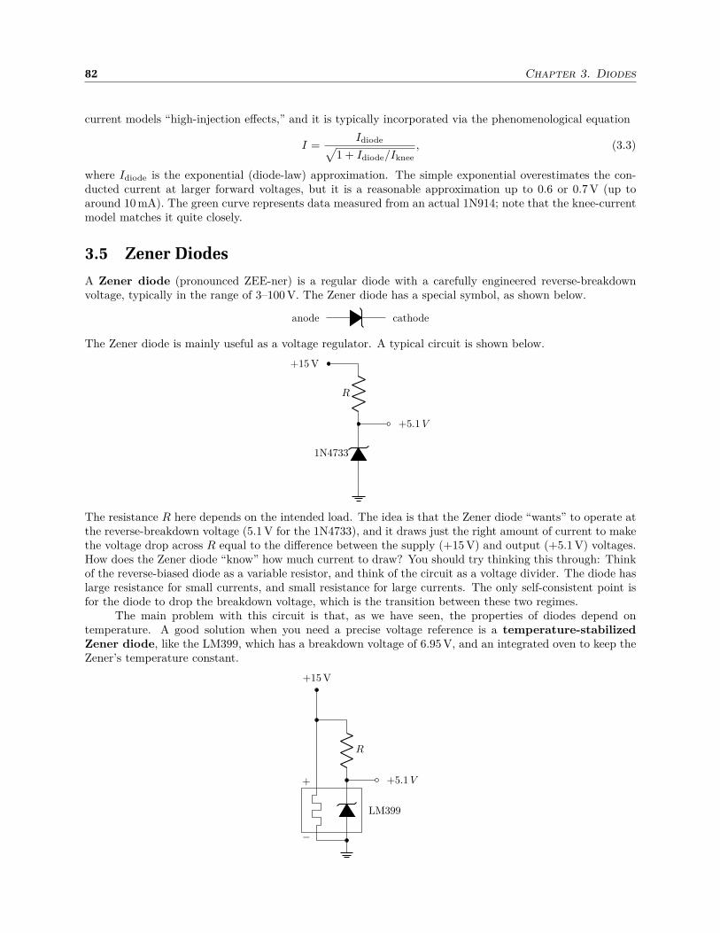
82 Chapter 3. Diodes
current models “high-injection effects,” and it is typically incorporated via the phenomenological equation
I =Idiode
√
1 + Idiode/Iknee
, (3.3)
where Idiode is the exponential (diode-law) approximation. The simple exponential overestimates the con-ducted current at larger forward voltages, but it is a reasonable approximation up to 0.6 or 0.7 V (up toaround 10 mA). The green curve represents data measured from an actual 1N914; note that the knee-currentmodel matches it quite closely.
3.5 Zener Diodes
A Zener diode (pronounced ZEE-ner) is a regular diode with a carefully engineered reverse-breakdownvoltage, typically in the range of 3–100 V. The Zener diode has a special symbol, as shown below.
anode cathode
The Zener diode is mainly useful as a voltage regulator. A typical circuit is shown below.
R
+15 V
1N4733
+5.1 V
The resistance R here depends on the intended load. The idea is that the Zener diode “wants” to operate atthe reverse-breakdown voltage (5.1 V for the 1N4733), and it draws just the right amount of current to makethe voltage drop across R equal to the difference between the supply (+15 V) and output (+5.1 V) voltages.How does the Zener diode “know” how much current to draw? You should try thinking this through: Thinkof the reverse-biased diode as a variable resistor, and think of the circuit as a voltage divider. The diode haslarge resistance for small currents, and small resistance for large currents. The only self-consistent point isfor the diode to drop the breakdown voltage, which is the transition between these two regimes.
The main problem with this circuit is that, as we have seen, the properties of diodes depend ontemperature. A good solution when you need a precise voltage reference is a temperature-stabilizedZener diode, like the LM399, which has a breakdown voltage of 6.95 V, and an integrated oven to keep theZener’s temperature constant.
LM399
+
−
R
+15 V
+5.1 V

3.6 Rectifier Circuits 83
The extra two connections are the power-supply leads for the oven heater. Note that this circuit can drawlarge (up to 200 mA) for the first few seconds after the circuit is turned on, while the oven temperaturestabilizes. You can then obtain other reference voltages using a voltage divider or an op-amp circuit tomultiply the voltage by a known factor—something we will get to later.
3.6 Rectifier Circuits
3.6.1 Half-Wave Rectifier
One of the main uses of a diode is as a rectifier, or something that changes an alternating-current (ac)signal into a direct-current (dc) signal. This is especially useful for changing the line voltage (120 V in theU.S.) into a dc voltage (e.g., for a power supply), after stepping the line voltage down (or up) by some factorusing a transformer. The simplest example of a rectifier circuit is the half-wave rectifier, which uses onlya single diode.
RloadVin
Here, the supply (with amplitude Vin) creates a voltage across the load (represented schematically here by aload resistor Rload); since current only flows in one direction, the supply can only impose a positive voltageacross the resistor, and the voltage during forward conduction is always a diode drop below the voltage ofthe power supply.
V
t
VinVino-o0.7oV
This is not very much like a dc voltage, and not a very good dc power supply. The trick to getting a betterdc signal is to add a smoothing capacitor across the load, as in the schematic below.
RloadVin Cfilter
Then the circuit charges the capacitor through the diode to a maximum of Vin, less the diode drop. Whenthe rectified voltage falls away, the capacitor “props up” the output voltage, which decays exponentially witha 1/e time of RloadCfilter. The net result is shown below.
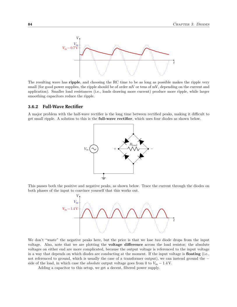
84 Chapter 3. Diodes
V
t
VinVino-o0.7oV
The resulting wave has ripple, and choosing the RC time to be as long as possible makes the ripple verysmall (for good power supplies, the ripple should be of order mV or tens of mV, depending on the current andapplication). Smaller load resistances (i.e., loads drawing more current) produce more ripple, while largersmoothing capacitors reduce the ripple.
3.6.2 Full-Wave Rectifier
A major problem with the half-wave rectifier is the long time between rectified peaks, making it difficult toget small ripple. A solution to this is the full-wave rectifier, which uses four diodes as shown below.
Rload
Vin + −
This passes both the positive and negative peaks, as shown below. Trace the current through the diodes onboth phases of the input to convince yourself that this works out.
V
t
Vin
Vino-o1.4oV
We don’t “waste” the negative peaks here, but the price is that we lose two diode drops from the inputvoltage. Also, note that we are plotting the voltage difference across the load resistor; the absolutevoltages on either end are more complicated, because the output voltage is referenced to the input voltagein a way that depends on which diodes are conducting at the moment. If the input voltage is floating (i.e.,not referenced to ground, which is usually the case of a transformer output), we can instead ground the −side of the load, in which case the absolute output voltage goes from 0 to Vin − 1.4 V.
Adding a capacitor to this setup, we get a decent, filtered power supply.
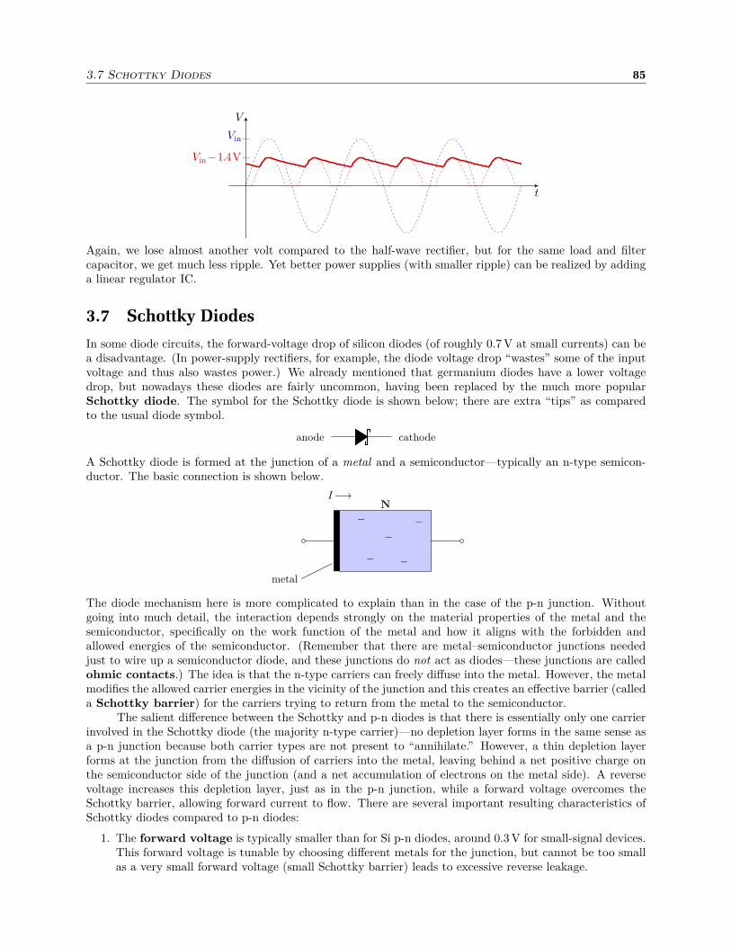
3.7 Schottky Diodes 85
V
t
Vin
Vino-o1.4oV
Again, we lose almost another volt compared to the half-wave rectifier, but for the same load and filtercapacitor, we get much less ripple. Yet better power supplies (with smaller ripple) can be realized by addinga linear regulator IC.
3.7 Schottky Diodes
In some diode circuits, the forward-voltage drop of silicon diodes (of roughly 0.7 V at small currents) can bea disadvantage. (In power-supply rectifiers, for example, the diode voltage drop “wastes” some of the inputvoltage and thus also wastes power.) We already mentioned that germanium diodes have a lower voltagedrop, but nowadays these diodes are fairly uncommon, having been replaced by the much more popularSchottky diode. The symbol for the Schottky diode is shown below; there are extra “tips” as comparedto the usual diode symbol.
anode cathode
A Schottky diode is formed at the junction of a metal and a semiconductor—typically an n-type semicon-ductor. The basic connection is shown below.
I−→
metal
N
−
−
−−
−
The diode mechanism here is more complicated to explain than in the case of the p-n junction. Withoutgoing into much detail, the interaction depends strongly on the material properties of the metal and thesemiconductor, specifically on the work function of the metal and how it aligns with the forbidden andallowed energies of the semiconductor. (Remember that there are metal–semiconductor junctions neededjust to wire up a semiconductor diode, and these junctions do not act as diodes—these junctions are calledohmic contacts.) The idea is that the n-type carriers can freely diffuse into the metal. However, the metalmodifies the allowed carrier energies in the vicinity of the junction and this creates an effective barrier (calleda Schottky barrier) for the carriers trying to return from the metal to the semiconductor.
The salient difference between the Schottky and p-n diodes is that there is essentially only one carrierinvolved in the Schottky diode (the majority n-type carrier)—no depletion layer forms in the same sense asa p-n junction because both carrier types are not present to “annihilate.” However, a thin depletion layerforms at the junction from the diffusion of carriers into the metal, leaving behind a net positive charge onthe semiconductor side of the junction (and a net accumulation of electrons on the metal side). A reversevoltage increases this depletion layer, just as in the p-n junction, while a forward voltage overcomes theSchottky barrier, allowing forward current to flow. There are several important resulting characteristics ofSchottky diodes compared to p-n diodes:
1. The forward voltage is typically smaller than for Si p-n diodes, around 0.3 V for small-signal devices.This forward voltage is tunable by choosing different metals for the junction, but cannot be too smallas a very small forward voltage (small Schottky barrier) leads to excessive reverse leakage.

86 Chapter 3. Diodes
2. Reverse leakage is typically worse in Schottky diodes.
3. Reverse breakdown also typically occurs at lower voltages in Schottky diodes.
4. A main advantage of Schottky diodes is fast switching or fast reverse recovery. The idea is thatwhen a p-n diode goes from reverse to forward bias, there is a delay before forward conduction starts,because the minority carriers on each side of the junction (e.g., the n-type carriers in the p-type region)must be returned to their original side so that conduction can begin. Because Schottky diodes only usemajority carriers, there is no such issue with “minority carrier storage,” and so their reverse recoveryis much faster. For example, the p-n reverse recovery times range from 4 ns (1N914 small-signal diode)to 30 µs (1N4011, 1-A rectifier). The 1N5711 small-signal Schottky diode specifies a 1-ns maximumreverse recovery time, and the 1N5819 small-signal Schottky does not even specify a maximum recoverytime (just advertising “extremely fast switching”).
Other than the differences noted here, Schottky diodes are functionally equivalent to p-n diodes, andare available in anything ranging from small-signal diodes to high-current power rectifiers.
3.8 Circuit Practice
3.8.1 Cockroft–Walton Multiplier
Explain how the circuit below, the Cockcroft-Walton multiplier, works. The multiplier is driven by anac source of amplitude Vin, and each “stage” of the multiplier consists of two capacitors and two diodes.The output after N stages is (in steady state) a dc voltage of 2NV . Three stages are shown in the examplebelow.
Vin
2Vin 4Vin
6Vin
Assume ideal capacitors and diodes (and think about why it is reasonable to ignore the forward voltage dropof the diodes in this kind of circuit).
Solution. The idea in multiplying voltages is to get high voltages, so the input ac voltage would be of theorder of 1 kV, in which case a diode drop of 0.7 V makes little difference.
To analyze the circuit, we will first trace the voltages when the input voltage has swung low. Currentflows across the first diode to charge the first capacitor.
I
Vin
−Vin 0
Then, on the positive-voltage phase, the absolute voltage of the first capacitor increases, but the voltageacross it stays the same. Current flows to charge the second capacitor.
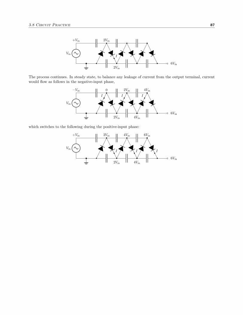
3.8 Circuit Practice 87
IVin
2Vin
6Vin
+Vin 2Vin
The process continues. In steady state, to balance any leakage of current from the output terminal, currentwould flow as follows in the negative-input phase,
I I I
Vin
−Vin
2Vin 4Vin
6Vin
0 2Vin 4Vin
which switches to the following during the positive-input phase:
I I IVin
+Vin
2Vin 4Vin
6Vin
2Vin 4Vin 6Vin
88 Chapter 3. Diodes
3.9 Exercises
Problem 3.1
Every diode has some intrinsic capacitance.
(a) What is the origin of this capacitance in a p–n junction diode? Be brief.
(b) If the diode is reverse-biased, does the capacitance increase, decrease, or stay the same withincreasing reverse voltage? More importantly: Why? (Be brief.)
Problem 3.2
Consider the zener-diode voltage regulator shown below.
R
+15 V
1N4738
Vout
Suppose you design this circuit to drive (supply) a load resistance RL.
(a) What is Vout?
(b) If R = 1 kΩ, what is the smallest RL that the circuit can handle without “sagging” the outputvoltage?
(c) What should be the power rating of the resistor R? Be explicit about your assumptions.
Problem 3.3
Consider the half-wave rectifier circuit shown below. The ac input voltage to the circuit is a 60 Hzsignal from a power transformer.
MR752
47000 µF RL
Vout
+6.3 V (rms)
(a) What is the peak output voltage across the load resistor, assuming RL = 10 Ω? Account for thevoltage drop across the diode (look it up!).
(b) Estimate the voltage ripple, assuming the same load resistance.
Problem 3.4
Sketch the analogous full-wave-rectifier-bridge circuit to the circuit in Problem 3.3, and repeat thecalculations.
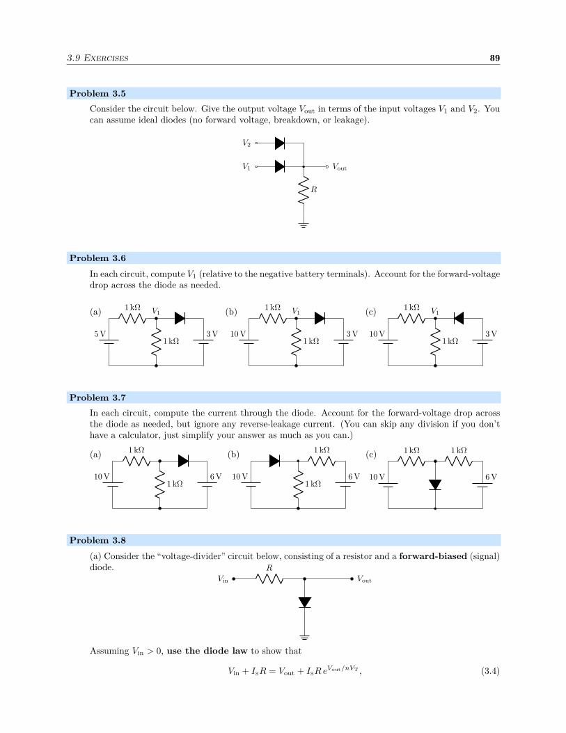
3.9 Exercises 89
Problem 3.5
Consider the circuit below. Give the output voltage Vout in terms of the input voltages V1 and V2. Youcan assume ideal diodes (no forward voltage, breakdown, or leakage).
V1
V2
R
Vout
Problem 3.6
In each circuit, compute V1 (relative to the negative battery terminals). Account for the forward-voltagedrop across the diode as needed.
(a)1 kΩ
1 kΩ5 V 3 V
V1 (b)1 kΩ
1 kΩ10 V 3 V
V1 (c)1 kΩ
1 kΩ10 V 3 V
V1
Problem 3.7
In each circuit, compute the current through the diode. Account for the forward-voltage drop acrossthe diode as needed, but ignore any reverse-leakage current. (You can skip any division if you don’thave a calculator, just simplify your answer as much as you can.)
(a)1 kΩ
1 kΩ10 V 6 V
(b)
1 kΩ10 V 6 V
1 kΩ(c) 1 kΩ
10 V 6 V
1 kΩ
Problem 3.8
(a) Consider the “voltage-divider” circuit below, consisting of a resistor and a forward-biased (signal)diode. R
Vin Vout
Assuming Vin > 0, use the diode law to show that
Vin + ISR = Vout + ISR eVout/nVT , (3.4)

90 Chapter 3. Diodes
which determines Vout in terms of Vin, R, and T .
(b) Does the idea of a Thévenin-equivalent circuit make sense for this circuit? If yes, give the Thévenin-equivalent voltage and resistance. If no, explain briefly why not.
(c) Does Vout increase or decrease with T? (Assume R, IS, and n are independent of temperature.)
(d) Obtain an explicit solution to the relation you derived in (a) as follows. Rearrange the equation tocombine the parts that depend on Vout in the form x ex, where
x =Vin − Vout + ISR
nVT. (3.5)
That is, you should obtain an equation of the form x ex = y, where y is independent of Vout. Then usethe defining relation
W (z) eW (z) = z (3.6)
of the Lambert W function to show that
Vout = Vin + ISR− (nVT ) W
(
ISR
nVTe(Vin+ISR)/nVT
)
(3.7)
is the explicit solution of the relation (3.4).

Chapter 4
Bipolar Junction Transistors
4.1 Overview
A bipolar junction transistor (BJT) is our first example of a device that is both nonlinear and active—active, in the sense that the device should be “powered,” or to say it another way, it uses one signal tomodify another signal. At first, it’s a bit counterintuitive to have a device with three terminals, but roughlyspeaking, you can think of it functionally as having a pair of input terminals and a pair of output terminals,but one terminal is “shared” between the input and the output.
BJTs come in two flavors: NPN and PNP, which refers to the stack of doped semiconductors that formthe transistor. The schematic construction of the NPN transistor is shown below: the name just gives theorder of the layers from top to bottom (or bottom to top).
N
N
P
collector
emitter
base
−
−
−−
−
++
−
−
−−
−
That is, the NPN transistor is a p-type semiconductor sandwiched in between two n-type semiconductors.However, the important thing is that the inner p-type layer is thin and lightly doped. The light dopingmeans that there are relatively few p-type carriers in the p-type layer. The PNP transistor is pretty muchthe same thing, except for interchanging p-type and n-type layers. All the analysis here will go through tothat case under this interchange, provided we also reverse all the currents and voltage differences. Thus we’llstick to the NPN case here (which is the more common case; usually, PNPs are only found when they arepaired in some way with an NPN, in part because NPNs are easier to make well).
The schematic symbols for NPN and PNP transistors are shown below.
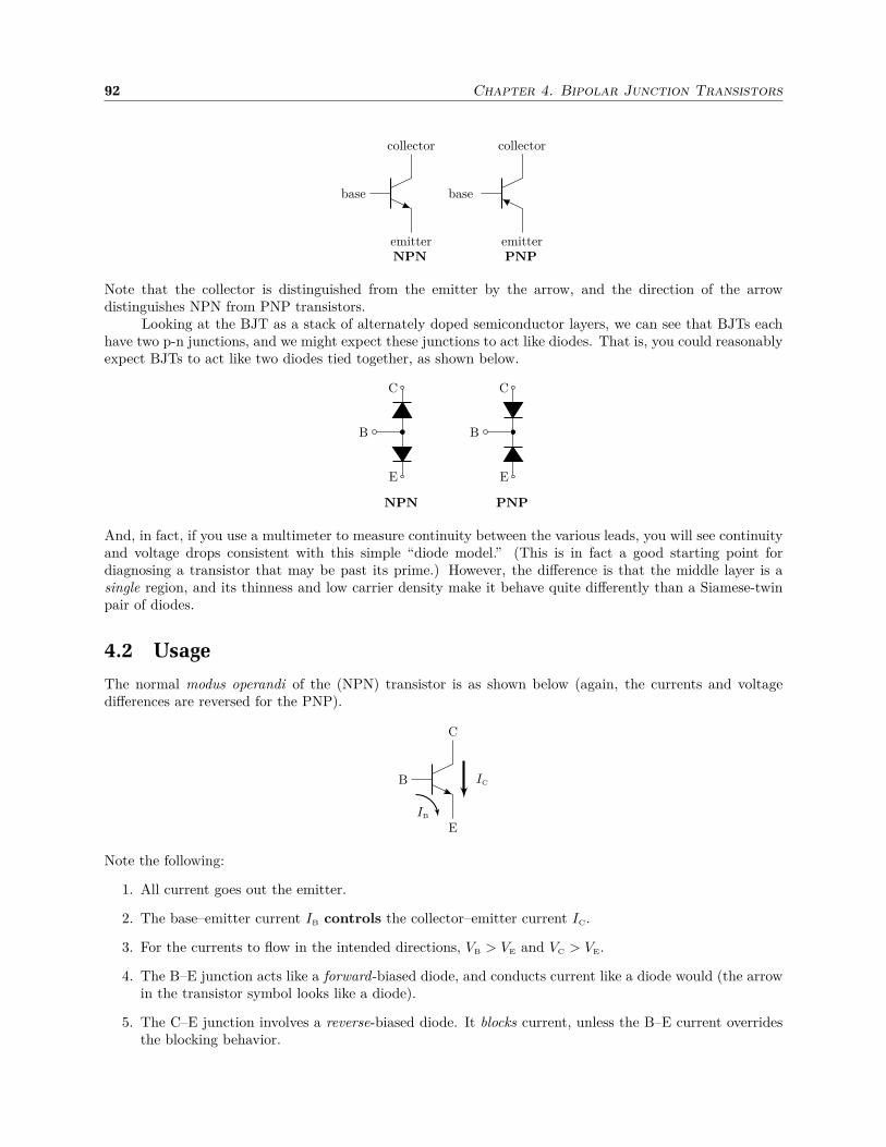
92 Chapter 4. Bipolar Junction Transistors
base
collector
emitterNPN
base
collector
emitterPNP
Note that the collector is distinguished from the emitter by the arrow, and the direction of the arrowdistinguishes NPN from PNP transistors.
Looking at the BJT as a stack of alternately doped semiconductor layers, we can see that BJTs eachhave two p-n junctions, and we might expect these junctions to act like diodes. That is, you could reasonablyexpect BJTs to act like two diodes tied together, as shown below.
B
C
E
NPN
B
C
E
PNP
And, in fact, if you use a multimeter to measure continuity between the various leads, you will see continuityand voltage drops consistent with this simple “diode model.” (This is in fact a good starting point fordiagnosing a transistor that may be past its prime.) However, the difference is that the middle layer is asingle region, and its thinness and low carrier density make it behave quite differently than a Siamese-twinpair of diodes.
4.2 Usage
The normal modus operandi of the (NPN) transistor is as shown below (again, the currents and voltagedifferences are reversed for the PNP).
B
C
E
IC
IB
Note the following:
1. All current goes out the emitter.
2. The base–emitter current IB controls the collector–emitter current IC.
3. For the currents to flow in the intended directions, VB > VE and VC > VE.
4. The B–E junction acts like a forward-biased diode, and conducts current like a diode would (the arrowin the transistor symbol looks like a diode).
5. The C–E junction involves a reverse-biased diode. It blocks current, unless the B–E current overridesthe blocking behavior.
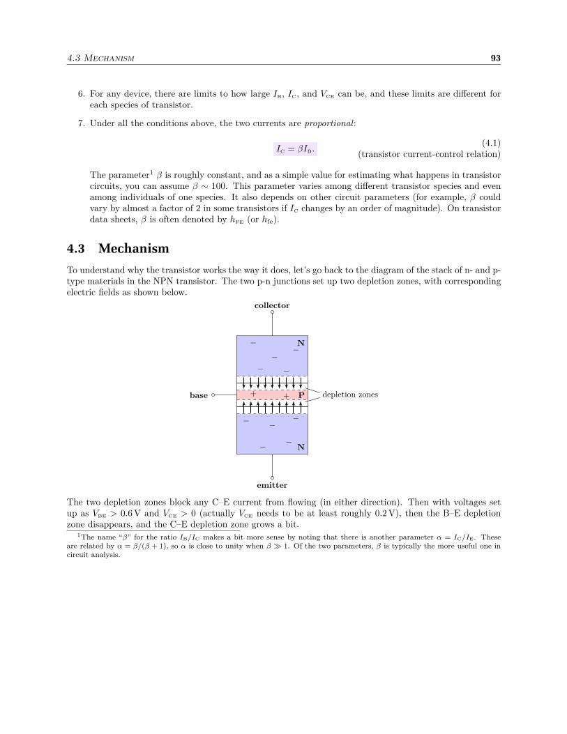
4.3 Mechanism 93
6. For any device, there are limits to how large IB, IC, and VCE can be, and these limits are different foreach species of transistor.
7. Under all the conditions above, the two currents are proportional:
IC = βIB.(4.1)
(transistor current-control relation)
The parameter1 β is roughly constant, and as a simple value for estimating what happens in transistorcircuits, you can assume β ∼ 100. This parameter varies among different transistor species and evenamong individuals of one species. It also depends on other circuit parameters (for example, β couldvary by almost a factor of 2 in some transistors if IC changes by an order of magnitude). On transistordata sheets, β is often denoted by hFE (or hfe).
4.3 Mechanism
To understand why the transistor works the way it does, let’s go back to the diagram of the stack of n- and p-type materials in the NPN transistor. The two p-n junctions set up two depletion zones, with correspondingelectric fields as shown below.
depletion zones
N
N
P
collector
emitter
base
−
−
−−
−
+ +
−
−−
−
−
The two depletion zones block any C–E current from flowing (in either direction). Then with voltages setup as VBE > 0.6 V and VCE > 0 (actually VCE needs to be at least roughly 0.2 V), then the B–E depletionzone disappears, and the C–E depletion zone grows a bit.
1The name “β” for the ratio IB/IC makes a bit more sense by noting that there is another parameter α = IC/IE. Theseare related by α = β/(β + 1), so α is close to unity when β ≫ 1. Of the two parameters, β is typically the more useful one incircuit analysis.
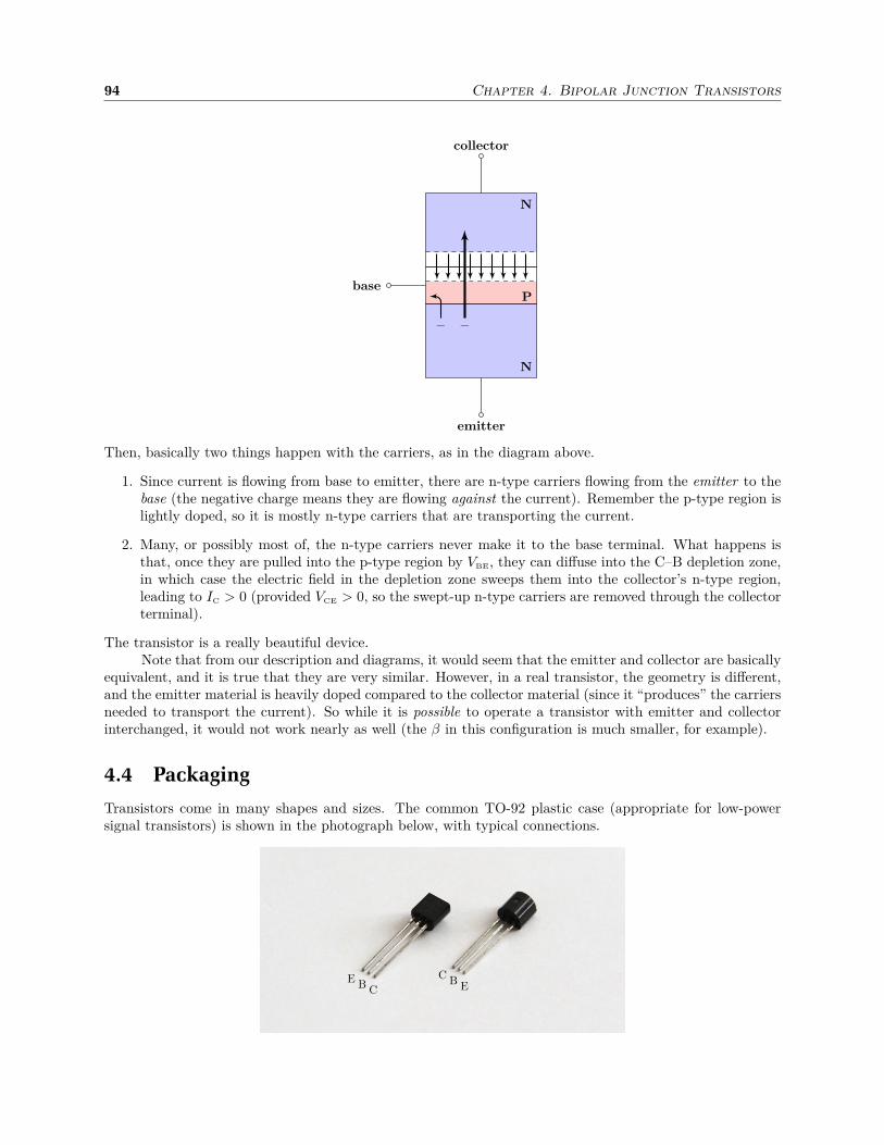
94 Chapter 4. Bipolar Junction Transistors
− −
N
N
P
collector
emitter
base
Then, basically two things happen with the carriers, as in the diagram above.
1. Since current is flowing from base to emitter, there are n-type carriers flowing from the emitter to thebase (the negative charge means they are flowing against the current). Remember the p-type region islightly doped, so it is mostly n-type carriers that are transporting the current.
2. Many, or possibly most of, the n-type carriers never make it to the base terminal. What happens isthat, once they are pulled into the p-type region by VBE, they can diffuse into the C–B depletion zone,in which case the electric field in the depletion zone sweeps them into the collector’s n-type region,leading to IC > 0 (provided VCE > 0, so the swept-up n-type carriers are removed through the collectorterminal).
The transistor is a really beautiful device.Note that from our description and diagrams, it would seem that the emitter and collector are basically
equivalent, and it is true that they are very similar. However, in a real transistor, the geometry is different,and the emitter material is heavily doped compared to the collector material (since it “produces” the carriersneeded to transport the current). So while it is possible to operate a transistor with emitter and collectorinterchanged, it would not work nearly as well (the β in this configuration is much smaller, for example).
4.4 Packaging
Transistors come in many shapes and sizes. The common TO-92 plastic case (appropriate for low-powersignal transistors) is shown in the photograph below, with typical connections.
E B C
C B E
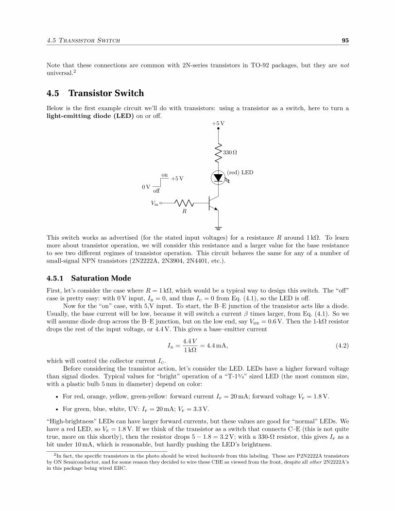
4.5 Transistor Switch 95
Note that these connections are common with 2N-series transistors in TO-92 packages, but they are not
universal.2
4.5 Transistor Switch
Below is the first example circuit we’ll do with transistors: using a transistor as a switch, here to turn alight-emitting diode (LED) on or off.
off
on
0 V
+5 V
R
Vin
+5 V
330 Ω
(red) LED
This switch works as advertised (for the stated input voltages) for a resistance R around 1 kΩ. To learnmore about transistor operation, we will consider this resistance and a larger value for the base resistanceto see two different regimes of transistor operation. This circuit behaves the same for any of a number ofsmall-signal NPN transistors (2N2222A, 2N3904, 2N4401, etc.).
4.5.1 Saturation Mode
First, let’s consider the case where R = 1 kΩ, which would be a typical way to design this switch. The “off”case is pretty easy: with 0 V input, IB = 0, and thus IC = 0 from Eq. (4.1), so the LED is off.
Now for the “on” case, with 5,V input. To start, the B–E junction of the transistor acts like a diode.Usually, the base current will be low, because it will switch a current β times larger, from Eq. (4.1). So wewill assume diode drop across the B–E junction, but on the low end, say VBE = 0.6 V. Then the 1-kΩ resistordrops the rest of the input voltage, or 4.4 V. This gives a base–emitter current
IB =4.4 V
1 kΩ= 4.4 mA, (4.2)
which will control the collector current IC.Before considering the transistor action, let’s consider the LED. LEDs have a higher forward voltage
than signal diodes. Typical values for “bright” operation of a “T-13⁄4” sized LED (the most common size,with a plastic bulb 5 mm in diameter) depend on color:
• For red, orange, yellow, green-yellow: forward current IF = 20 mA; forward voltage VF = 1.8 V.
• For green, blue, white, UV: IF = 20 mA; VF = 3.3 V.
“High-brightness” LEDs can have larger forward currents, but these values are good for “normal” LEDs. Wehave a red LED, so VF = 1.8 V. If we think of the transistor as a switch that connects C–E (this is not quitetrue, more on this shortly), then the resistor drops 5− 1.8 = 3.2 V; with a 330-Ω resistor, this gives IF as abit under 10 mA, which is reasonable, but hardly pushing the LED’s brightness.
2In fact, the specific transistors in the photo should be wired backwards from this labeling. These are P2N2222A transistorsby ON Semiconductor, and for some reason they decided to wire these CBE as viewed from the front, despite all other 2N2222A’sin this package being wired EBC.

96 Chapter 4. Bipolar Junction Transistors
But what does the transistor want to do? Eq. (4.1) says that IC should be β times IB; assumingβ ∼ 100, then IC ∼ 440 mA. But, as we found out, with the LED and resistor voltage drops, IC can’tpossibly be this high (the transistor can’t have a negative voltage drop, for example). In fact, the transistordrop VCE can’t be less than about 0.2 V, so the resistor actually drops about 3.0 V. With the 330-Ω resistor,this gives IC = IF ≈ 9.1 mA.
This mode of transistor operation is called saturation mode: as a switch, the transistor is “wideopen,” and the current IC is limited by external elements (here, LED and 330-Ω resistor), not the transistor.Of course, the current-limiting resistor could be reduced somewhat (say, to 150 Ω) for a brighter LED here.[The term “saturation” comes from the base region being saturated by (minority) carriers from both thecollector and emitter regions; note that in saturation the base–collector junction is also slightly forward-biased.)
The important thing to notice in this example is that a high-impedance source (1 kΩ, from the baseresistor, plus any impedance of the input voltage source) controls a higher-current load via the transistor.
4.5.2 Forward-Active Mode
Now suppose R = 100 kΩ in the same circuit. Then the base current is two orders of magnitude smaller, or44 µA. The transistor tries to set IC ∼ 100IB = 4.4 mA, and now this is certainly possible for the transistor.Just to double check, the voltage drop across the 330-Ω resistor is 330 Ω × 4.4 mA = 1.5 V. Then removingthe resistor and LED drops, VCE = 5 V − 1.8 V − 1.5 V = 1.7 V. Now it is the transistor that is regulatingthe current via its voltage drop. This is called the forward-active mode of the transistor, and it is inthis regime that the transistor can act as an amplifier with some gain (the saturation mode is a kind of“infinite-gain” amplification).
4.5.3 Summary
Let’s just summarize the difference between saturation and forward-active modes in the switching circuit,because this can be a bit confusing the first time through, and it’s important to understand the differenceintuitively.
In forward-active mode, the base current IB controlled the collector current IC (and thus the LEDcurrent) via the relation IC = βIB. The transistor “regulates” IC by adjusting the voltage VCE to the properamount. We know the current is set by the voltage drop across the 330-Ω resistor: the larger the resistordrop, the larger the current. This means that VCE is smaller for larger currents, because more of the supplyvoltage must be taken up by the resistor.
In saturation mode, the transistor relation doesn’t hold. That’s because the base current makes thetransistor “want” more current than the 330-Ω resistor will allow. The transistor normally tries to drivemore current by reducing VCE, but it can’t do so below zero (or more precisely, below about 0.2 V if IC > 0),so IC < βIB.
So you can really think of the transistor relation as being more like IC ≤ βIB. Both the transistor andan external element (resistor) will want to limit the current; whichever wants less current is the one thatwins.
4.6 Emitter Follower
As our second transistor circuit, we’ll continue with a transistor in forward-active mode. Below is theemitter follower, where the output voltage is intended to “follow,” or match, the input voltage. It is anamplifier in the sense of being an amplifier for current.
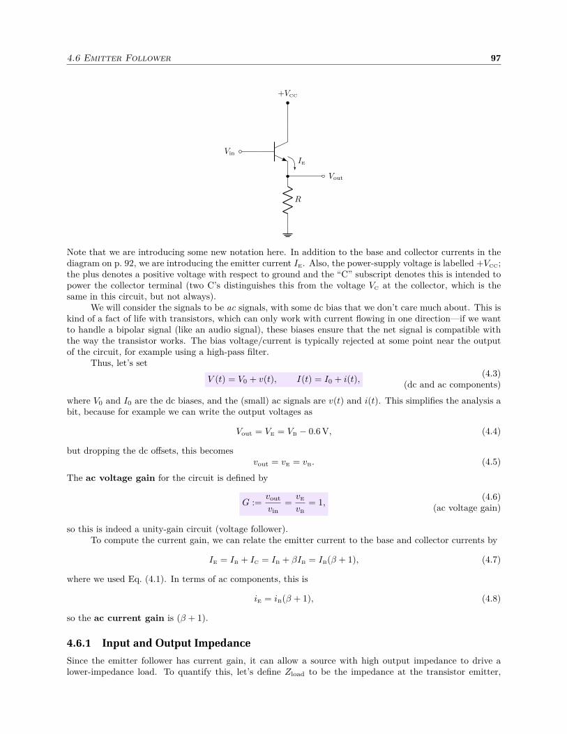
4.6 Emitter Follower 97
IE
Vin
R
+VCC
Vout
Note that we are introducing some new notation here. In addition to the base and collector currents in thediagram on p. 92, we are introducing the emitter current IE. Also, the power-supply voltage is labelled +VCC;the plus denotes a positive voltage with respect to ground and the “C” subscript denotes this is intended topower the collector terminal (two C’s distinguishes this from the voltage VC at the collector, which is thesame in this circuit, but not always).
We will consider the signals to be ac signals, with some dc bias that we don’t care much about. This iskind of a fact of life with transistors, which can only work with current flowing in one direction—if we wantto handle a bipolar signal (like an audio signal), these biases ensure that the net signal is compatible withthe way the transistor works. The bias voltage/current is typically rejected at some point near the outputof the circuit, for example using a high-pass filter.
Thus, let’s set
V (t) = V0 + v(t), I(t) = I0 + i(t),(4.3)
(dc and ac components)
where V0 and I0 are the dc biases, and the (small) ac signals are v(t) and i(t). This simplifies the analysis abit, because for example we can write the output voltages as
Vout = VE = VB − 0.6 V, (4.4)
but dropping the dc offsets, this becomesvout = vE = vB. (4.5)
The ac voltage gain for the circuit is defined by
G :=vout
vin=
vE
vB
= 1,(4.6)
(ac voltage gain)
so this is indeed a unity-gain circuit (voltage follower).To compute the current gain, we can relate the emitter current to the base and collector currents by
IE = IB + IC = IB + βIB = IB(β + 1), (4.7)
where we used Eq. (4.1). In terms of ac components, this is
iE = iB(β + 1), (4.8)
so the ac current gain is (β + 1).
4.6.1 Input and Output Impedance
Since the emitter follower has current gain, it can allow a source with high output impedance to drive alower-impedance load. To quantify this, let’s define Zload to be the impedance at the transistor emitter,

98 Chapter 4. Bipolar Junction Transistors
which is R in parallel with any other load impedance attached to the Vout terminal. Then we can calculate
iB =iE
β + 1=
vE
Zload(β + 1)=
vB
Zload(β + 1). (4.9)
Here, we used the current gain (4.8), then vE = iER, then vE = vB. Then we can define the input impedanceof the amplifier by
Zin :=vin
iin.
(4.10)(input impedance, definition)
Writing the input voltage and current in terms of the base voltage and current,
Zin =vB
iB
, (4.11)
and then using Eq. (4.9),
Zin = Zload(β + 1).(4.12)
(input impedance, emitter follower)
We can interpret this as follows: Without the transistor, the input vin would have to “drive” the loadimpedance (the resistor R and other connected stuff) directly, as shown below
vin
Zload = R‖(other loads)
The effect of the transistor is to multiply the resistor value by (β + 1), so effectively the impedance is about100 times larger, and thus much easier to drive—the transistor is supplying most of the current via thecollector, so the voltage source driving the resistor doesn’t have to supply much current at all. Thus, theequivalent circuit with the transistor is shown below.
vin
Zin = (β + 1)Zload
vB
Of course, we can think of this (Thévenin) equivalent circuit because the transistor is acting as a linearamplifier.
We can also define an output impedance as
Zout :=vout
iout.
(4.13)(output impedance, definition)
Manipulating this a bit,
Zout =vin
iE
=vin
iB(β + 1), (4.14)
and then defining the source impedance
Zsource :=vin
iB
(4.15)(impedance of input source)
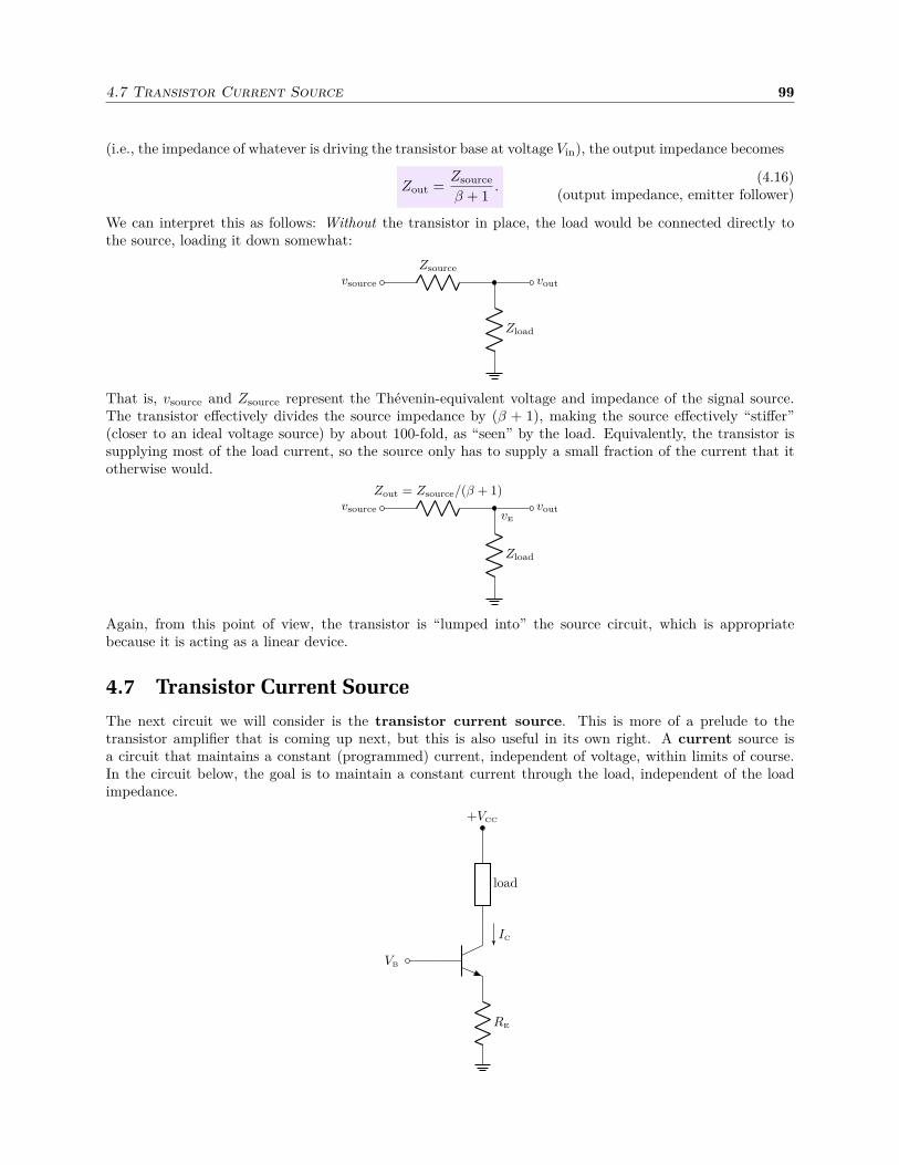
4.7 Transistor Current Source 99
(i.e., the impedance of whatever is driving the transistor base at voltage Vin), the output impedance becomes
Zout =Zsource
β + 1.
(4.16)(output impedance, emitter follower)
We can interpret this as follows: Without the transistor in place, the load would be connected directly tothe source, loading it down somewhat:
vsource
Zsource
vout
Zload
That is, vsource and Zsource represent the Thévenin-equivalent voltage and impedance of the signal source.The transistor effectively divides the source impedance by (β + 1), making the source effectively “stiffer”(closer to an ideal voltage source) by about 100-fold, as “seen” by the load. Equivalently, the transistor issupplying most of the load current, so the source only has to supply a small fraction of the current that itotherwise would.
vsource
Zout = Zsource/(β + 1)vout
Zload
vE
Again, from this point of view, the transistor is “lumped into” the source circuit, which is appropriatebecause it is acting as a linear device.
4.7 Transistor Current Source
The next circuit we will consider is the transistor current source. This is more of a prelude to thetransistor amplifier that is coming up next, but this is also useful in its own right. A current source isa circuit that maintains a constant (programmed) current, independent of voltage, within limits of course.In the circuit below, the goal is to maintain a constant current through the load, independent of the loadimpedance.
IC
VB
RE
load
+VCC
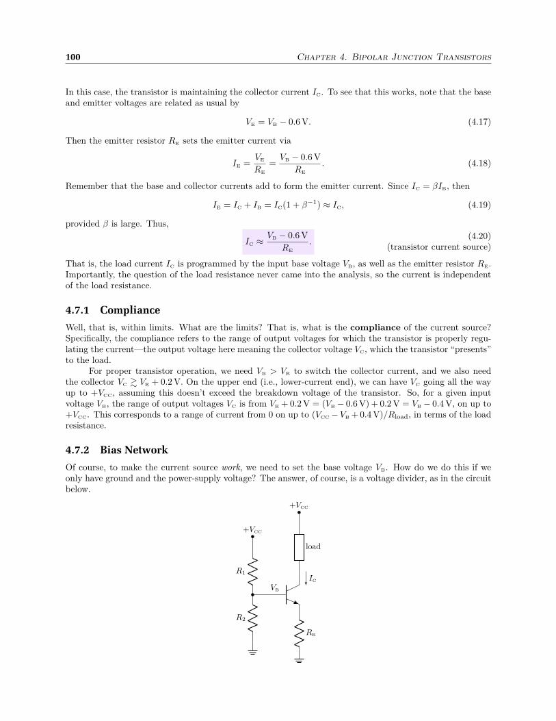
100 Chapter 4. Bipolar Junction Transistors
In this case, the transistor is maintaining the collector current IC. To see that this works, note that the baseand emitter voltages are related as usual by
VE = VB − 0.6 V. (4.17)
Then the emitter resistor RE sets the emitter current via
IE =VE
RE
=VB − 0.6 V
RE
. (4.18)
Remember that the base and collector currents add to form the emitter current. Since IC = βIB, then
IE = IC + IB = IC(1 + β−1) ≈ IC, (4.19)
provided β is large. Thus,
IC ≈VB − 0.6 V
RE
.(4.20)
(transistor current source)
That is, the load current IC is programmed by the input base voltage VB, as well as the emitter resistor RE.Importantly, the question of the load resistance never came into the analysis, so the current is independentof the load resistance.
4.7.1 Compliance
Well, that is, within limits. What are the limits? That is, what is the compliance of the current source?Specifically, the compliance refers to the range of output voltages for which the transistor is properly regu-lating the current—the output voltage here meaning the collector voltage VC, which the transistor “presents”to the load.
For proper transistor operation, we need VB > VE to switch the collector current, and we also needthe collector VC & VE + 0.2 V. On the upper end (i.e., lower-current end), we can have VC going all the wayup to +VCC, assuming this doesn’t exceed the breakdown voltage of the transistor. So, for a given inputvoltage VB, the range of output voltages VC is from VE + 0.2 V = (VB − 0.6 V) + 0.2 V = VB − 0.4 V, on up to+VCC. This corresponds to a range of current from 0 on up to (VCC−VB + 0.4 V)/Rload, in terms of the loadresistance.
4.7.2 Bias Network
Of course, to make the current source work, we need to set the base voltage VB. How do we do this if weonly have ground and the power-supply voltage? The answer, of course, is a voltage divider, as in the circuitbelow.
IC
R1
+VCC
R2
VB
RE
load
+VCC
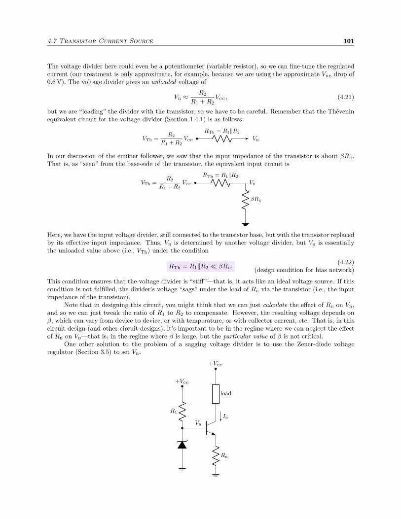
4.7 Transistor Current Source 101
The voltage divider here could even be a potentiometer (variable resistor), so we can fine-tune the regulatedcurrent (our treatment is only approximate, for example, because we are using the approximate VBE drop of0.6 V). The voltage divider gives an unloaded voltage of
VB ≈R2
R1 + R2VCC, (4.21)
but we are “loading” the divider with the transistor, so we have to be careful. Remember that the Théveninequivalent circuit for the voltage divider (Section 1.4.1) is as follows:
VTh =R2
R1 + R2VCC
RTh = R1‖R2
VB
In our discussion of the emitter follower, we saw that the input impedance of the transistor is about βRE.That is, as “seen” from the base-side of the transistor, the equivalent input circuit is
VTh =R2
R1 + R2VCC
RTh = R1‖R2
VB
βRE
Here, we have the input voltage divider, still connected to the transistor base, but with the transistor replacedby its effective input impedance. Thus, VB is determined by another voltage divider, but VB is essentiallythe unloaded value above (i.e., VTh) under the condition
RTh = R1‖R2 ≪ βRE.(4.22)
(design condition for bias network)
This condition ensures that the voltage divider is “stiff”—that is, it acts like an ideal voltage source. If thiscondition is not fulfilled, the divider’s voltage “sags” under the load of RE via the transistor (i.e., the inputimpedance of the transistor).
Note that in designing this circuit, you might think that we can just calculate the effect of RE on VB,and so we can just tweak the ratio of R1 to R2 to compensate. However, the resulting voltage depends onβ, which can vary from device to device, or with temperature, or with collector current, etc. That is, in thiscircuit design (and other circuit designs), it’s important to be in the regime where we can neglect the effectof RE on VB—that is, in the regime where β is large, but the particular value of β is not critical.
One other solution to the problem of a sagging voltage divider is to use the Zener-diode voltageregulator (Section 3.5) to set VB.
IC
R1
+VCC
VB
RE
load
+VCC
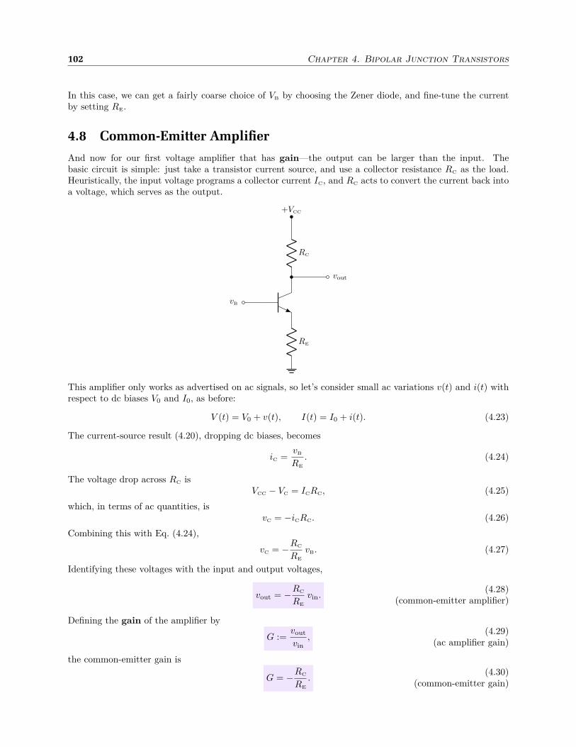
102 Chapter 4. Bipolar Junction Transistors
In this case, we can get a fairly coarse choice of VB by choosing the Zener diode, and fine-tune the currentby setting RE.
4.8 Common-Emitter Amplifier
And now for our first voltage amplifier that has gain—the output can be larger than the input. Thebasic circuit is simple: just take a transistor current source, and use a collector resistance RC as the load.Heuristically, the input voltage programs a collector current IC, and RC acts to convert the current back intoa voltage, which serves as the output.
vB
RE
RC
+VCC
vout
This amplifier only works as advertised on ac signals, so let’s consider small ac variations v(t) and i(t) withrespect to dc biases V0 and I0, as before:
V (t) = V0 + v(t), I(t) = I0 + i(t). (4.23)
The current-source result (4.20), dropping dc biases, becomes
iC =vB
RE
. (4.24)
The voltage drop across RC isVCC − VC = ICRC, (4.25)
which, in terms of ac quantities, isvC = −iCRC. (4.26)
Combining this with Eq. (4.24),
vC = −RC
RE
vB. (4.27)
Identifying these voltages with the input and output voltages,
vout = −RC
RE
vin.(4.28)
(common-emitter amplifier)
Defining the gain of the amplifier by
G :=vout
vin,
(4.29)(ac amplifier gain)
the common-emitter gain is
G = −RC
RE
.(4.30)
(common-emitter gain)

4.9 Bias Network (AC Coupling) 103
Then we see that the gain is negative, meaning the input ac signal is inverted at the output, and the ratioof collector and emitter resistors controls the gain.
For the sample-circuit numbers, we have G = −10.
4.9 Bias Network (AC Coupling)
As in the current source, we need an input network to set the dc bias. A nonzero bias is critical for theamplification of the ac signal: the B–E junction can only conduct in the forward direction, and so the inputsignal can’t cross through zero and still be amplified without a lot of distortion.
R1
+VCC
R2
C
vin
RE
RC
+VCC
vout
Here, the voltage divider sets the bias voltage, and the input capacitor only passes the ac part of the inputsignal.
Let’s go through the different parts of the circuit, and work out all the relevant parameters. As aconcrete example, we will use the parameters:
VCC = 15 V,
R1 = 56 kΩ,
R2 = 5.6 kΩ,
C = 0.1 µF,
RE = 330 Ω,
RC = 3.3 kΩ.
(4.31)
1. AC input impedance. The input circuit is a high-pass filter, with capacitance C. The Théveninresistance is the parallel resistance of R1 and R2, but we must also include the input impedance βRE
of the amplifier as an additional parallel resistance. Thus, at high frequencies when the capacitor actsas a short-circuit, the input impedance of the circuit is the Thévenin resistance, or R1‖R2‖βRE.
For this circuit, R1‖R2 = 5.1 kΩ. Also, βRE ≈ 100 kΩ, which is much larger than R1‖R2, soR1‖R2‖βRE ≈ R1‖R2 = 5.1 kΩ.
2. High-pass input. The corner frequency of the input network is
f3dB =1
2π(R1‖R2‖βRE)C.
(4.32)(input corner frequency)
For the circuit here, f3dB = 310 Hz.

104 Chapter 4. Bipolar Junction Transistors
3. Loading condition. It is good practice for the input impedance of the transistor to have negligibleeffect. That is, we should have
βRE ≫ R1‖R2, (4.33)
in which case the input impedance and corner frequency of the input network do not depend on β (andthus on temperature, etc.).
For the sample numbers here, we have already seen that we satisfy this condition.
4. Gain. From Eq. (4.30), the gain of the amplifier is
G = −RC
RE
. (4.34)
5. Output impedance. Because the transistor acts like a current source (with I insensitive to V ), thetransistor effectively presents a very large impedance at the output—a large change in voltage causeslittle change in the current. Thus the impedance at the output is the Thévenin resistance at that point,or the parallel impedance of the the collector with RC. Thus, we can take the output impedance of theamplifier to be approximately RC.
In this example, the output impedance of the amplifier is 3.3 kΩ.
6. Bias points. The bias at the input is just the voltage-divider voltage, including any correction fromβRE, which we usually want to ignore. In the circuit here, the 15 V supply is divided down to 1.36 V.
Why does this make sense? It’s important to note that the bias at the input isn’t critical in the senseof needing to be near the middle of the supply range. If we are doing a lot of amplification and wantto avoid clipping, though, the output should be close to the center of the supply. Let’s see if thisis the case. The emitter voltage is VE = VB − 0.6 V = 0.76 V. This programs a collector currentIC ≈ (VB − 0.6 V)/RE = 2.3 mA, from Eq. (4.20). Then the voltage drop across RC is 7.6 V which isabout half of VCC. Notice how the matching ratios of R1 to R2 and RC to RE lead to a sensible biasvoltage here, but because the (fixed) voltage VBE enters here, this rule does not always apply.
4.10 Transistor Differential Amplifier
Now we come to a more sophisticated transistor amplifier, the transistor differential amplifier. Schemat-ically, a differential amplifier has the following form:
−
+
Vout = A(Vin+ − Vin−)
Vin+
Vin−
That is, the output is the difference of the inputs (the signs at the inputs tell you which is subtracted fromwhich), and multiplied by the voltage gain factor A.
Why is a differential amplifier useful? For example:
1. In the transmission of signals, differential amplifiers give you noise immunity— if you transmit asignal on two lines (signal and ground), the same noise appears on each line, and gets cancelled out bya differential amplifier on the receiving end.
2. Differential amplifiers offer a straightforward way to implement negative feedback, which is a niceway to achieve close-to-ideal behavior in nearly every respect. We will go over this in much more detailwhen we get to op-amps.
The simplest realization of a differential amplifier uses two transistors. To understand this, first recallthe common-emitter amplifier.
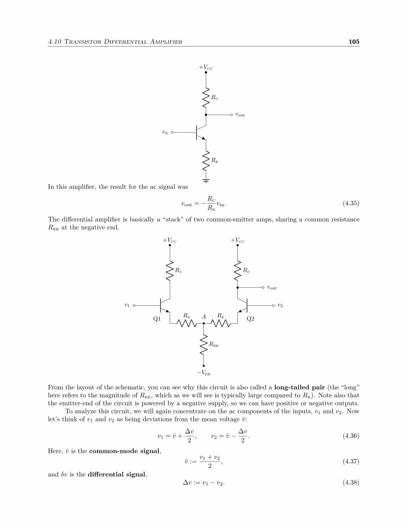
4.10 Transistor Differential Amplifier 105
vB
RE
RC
+VCC
vout
In this amplifier, the result for the ac signal was
vout = −RC
RE
vin. (4.35)
The differential amplifier is basically a “stack” of two common-emitter amps, sharing a common resistanceREE at the negative end.
Q1 Q2
v1 v2
RE REA
REE
−VEE
RC
+VCC
RC
+VCC
vout
From the layout of the schematic, you can see why this circuit is also called a long-tailed pair (the “long”here refers to the magnitude of REE, which as we will see is typically large compared to RE). Note also thatthe emitter-end of the circuit is powered by a negative supply, so we can have positive or negative outputs.
To analyze this circuit, we will again concentrate on the ac components of the inputs, v1 and v2. Nowlet’s think of v1 and v2 as being deviations from the mean voltage v:
v1 = v +∆v
2, v2 = v − ∆v
2. (4.36)
Here, v is the common-mode signal,
v :=v1 + v2
2, (4.37)
and δv is the differential signal,∆v := v1 − v2. (4.38)
106 Chapter 4. Bipolar Junction Transistors
Ideally, a differential amplifier responds only to the differential signal, and is insensitive to the common-modesignal.
4.10.1 Differential-Only Input
We will show that the circuit responds linearly to the inputs, so we can treat the differential and common-mode signals separately, just add them together to handle an arbitrary input signal. So first, let’s concentrateon only the differential signal. That is, setting v = 0, we have
v1 =∆v
2, v2 = −∆v
2. (4.39)
Then, just as in the emitter follower,vE1 = vB1 = v1, (4.40)
and similarlyvE2 = v2. (4.41)
At point A in the circuit, ignoring dc offsets, we have a 50% voltage divider between vE1 and vE2, so thevoltage is the average of these:
vA =vE1 + vE2
2=
v1 + v2
2= 0. (4.42)
We can interpret this as follows: The point A acts like the “ground” point for the two common-emitteramplifiers in this circuit. Since this point is stable with respect to differential inputs, the common-emitterresults carry through here, and in particular for the right-hand common-emitter amp,
vout = −RC
RE
v2, (4.43)
or in terms of the differential signal,
vout =RC
2RE
∆v.(4.44)
(differential response)
Note that the minus sign disappeared here, which is why it is sensible to take the output from the right-handtransistor. Thus, we have
Gdiff := − RC
2RE
.(4.45)
(differential gain factor)
as the differential gain factor for the amplifier.
4.10.2 Common-Mode-Only Input
Now we can focus on just the common-mode signal. That is, we take ∆v = 0, so that
v1 = v2 = v. (4.46)
Then applying Kirchoff’s law to the currents at point A,
iEE = iE1 + iE2 =: 2iE, (4.47)
since the two emitter currents are the same. Here, iE1 and iE2 are the (ac components of the) currents outeach emitter (both equal to iE), and iEE is the current through REE. Then applying Ohm’s law at point A,
vA = iEEREE = 2iEREE, (4.48)
and now Ohm’s law across either emitter resistor gives
iE =vE − vA
RE
=v − 2iEREE
RE
, (4.49)
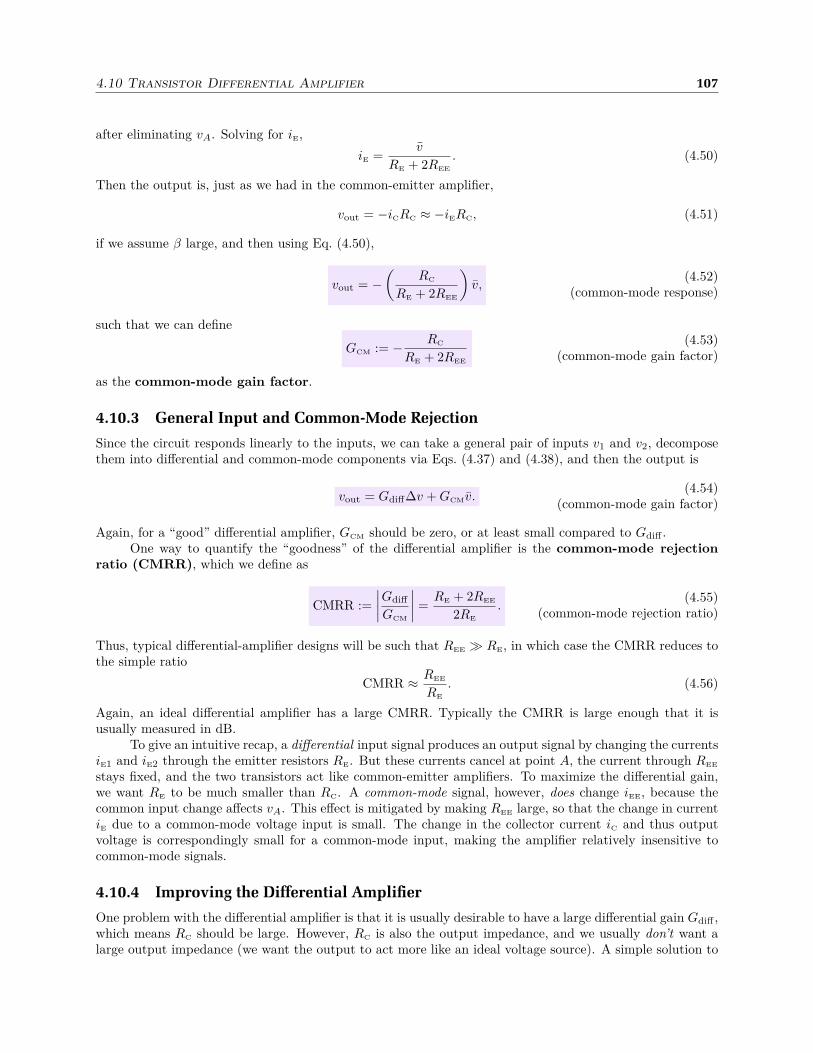
4.10 Transistor Differential Amplifier 107
after eliminating vA. Solving for iE,
iE =v
RE + 2REE
. (4.50)
Then the output is, just as we had in the common-emitter amplifier,
vout = −iCRC ≈ −iERC, (4.51)
if we assume β large, and then using Eq. (4.50),
vout = −(
RC
RE + 2REE
)
v,(4.52)
(common-mode response)
such that we can define
GCM := − RC
RE + 2REE
(4.53)(common-mode gain factor)
as the common-mode gain factor.
4.10.3 General Input and Common-Mode Rejection
Since the circuit responds linearly to the inputs, we can take a general pair of inputs v1 and v2, decomposethem into differential and common-mode components via Eqs. (4.37) and (4.38), and then the output is
vout = Gdiff∆v + GCMv.(4.54)
(common-mode gain factor)
Again, for a “good” differential amplifier, GCM should be zero, or at least small compared to Gdiff .One way to quantify the “goodness” of the differential amplifier is the common-mode rejection
ratio (CMRR), which we define as
CMRR :=
∣
∣
∣
∣
Gdiff
GCM
∣
∣
∣
∣
=RE + 2REE
2RE
.(4.55)
(common-mode rejection ratio)
Thus, typical differential-amplifier designs will be such that REE ≫ RE, in which case the CMRR reduces tothe simple ratio
CMRR ≈ REE
RE
. (4.56)
Again, an ideal differential amplifier has a large CMRR. Typically the CMRR is large enough that it isusually measured in dB.
To give an intuitive recap, a differential input signal produces an output signal by changing the currentsiE1 and iE2 through the emitter resistors RE. But these currents cancel at point A, the current through REE
stays fixed, and the two transistors act like common-emitter amplifiers. To maximize the differential gain,we want RE to be much smaller than RC. A common-mode signal, however, does change iEE, because thecommon input change affects vA. This effect is mitigated by making REE large, so that the change in currentiE due to a common-mode voltage input is small. The change in the collector current iC and thus outputvoltage is correspondingly small for a common-mode input, making the amplifier relatively insensitive tocommon-mode signals.
4.10.4 Improving the Differential Amplifier
One problem with the differential amplifier is that it is usually desirable to have a large differential gain Gdiff ,which means RC should be large. However, RC is also the output impedance, and we usually don’t want alarge output impedance (we want the output to act more like an ideal voltage source). A simple solution to
108 Chapter 4. Bipolar Junction Transistors
this is to buffer the output using an emitter follower, which will reduce the effective output impedance by afactor of β.
One trick to improving the CMRR comes from the observation from Eq. (4.55) that is that REE shouldbe large for a high CMRR. The idea is to replace REE by a current source, forcing iEE to be constant in thecommon-mode analysis above. This could be, for example, the transistor current source from Section 4.7, asshown in the diagram below.
v+ v−
RE RE
RC
+VCC
RC
+VCC
vout
REE
−VEE
R1
+VCC
−VEE
VB
Intuitively, a current source is like a very large REE, because it yields a small (essentially zero) change iniEE due to a change in vA. In fact one way to view the current source is that it regulates vA precisely tomaintain a constant iEE. In doing so, it prevents any change in collector currents due to a common-modeinput, and thus the circuit is insensitive to v. In the circuit above, note that the Zener diode sets the inputvoltage to the current source, which sets the current in combination with REE (the dc current through REE
should be set to give the desired dc voltage bias, typically 0 V, at the output).Finally, note that we can obtain a good CMRR by having RE ≪ REE. In fact, why can’t we just set
RE = 0? We can replace the resistors RE by shorts, but still these resistances will not be zero. In this case,the resistances will be the intrinsic resistance re of the transistors, to which we will return below.
4.11 Ebers–Moll Model
So far, we have been understanding transistor circuits using the crude current-control model, centeredon the equation [Eq. (4.1)]
IC = βIB, (4.57)
with β roughly constant. The crudeness is, of course, that β is not constant. Usually we try to design insuch a way that this doesn’t matter, but it is still useful to develop a better model of the transistor.
Recall the diode law (3.1), relating the diode current and voltage:
I = IS
(
eV/nVT − 1)
. (4.58)
Here, IS is the saturation current (reverse leakage current), n is the ideality, VT is the thermal voltage
VT :=kBT
e, (4.59)
4.11 Ebers–Moll Model 109
kB = 1.381 × 10⁻²³ J/K is the Boltzmann constant, and e = 1.602 × 10⁻¹⁹ C is the fundamental charge.The base–emitter junction of the transistor works much like a diode (recall that the collector current arisesas a “side effect” of the base–emitter current, since carriers headed initially towards the base are sweptinto the collector), and so a similar law serves as a simple model of transistor operation, the Ebers–Mollequation:3
IC = IS
(
eVBE/nVT − 1)
.(4.60)
(Ebers–Moll equation)
This relates the collector current IC to the base–emitter voltage VBE = VB − VE, via a transistor saturationcurrent IS. Unlike the current-control view of the β model of the transistor, the Ebers–Moll equation gives avoltage-control view of transistor operation. The control of IC via IB is only indirect, since IB is controlledby VBE via diode-like conduction. Thus, the transistor is a transconductance device (meaning a devicethat converts voltage to current). The Ebers–Moll model turns out to be accurate over a wide range ofcurrents, typically from nA–mA. Note that in what follows, we will drop the ideality factor n to simplifynotation somewhat without significantly affecting the calculations.
4.11.1 Magnitudes
To compare with what we know before, for a typical circuit analysis we assumed VBE ≈ 0.6 V, which is muchbigger than the thermal voltage VT (25.69 mV at 25C). Thus the exponential in the Ebers–Moll equation islarge compared to the 1, and so Eq. (4.60) becomes (setting n ≈ 1 to simplify the discussion)
IC ≈ IS eVBE/VT (4.61)
andIC ≫ IS. (4.62)
(To give a sense of scale for this latter statement, IS ≈ 1.75 pA for the common 2N4401, so this condition iscertainly fulfilled for typical transistor circuits when the B–E junction is forward-biased.) This also meansthat, as in the diode, that VBE is relatively insensitive to variations in the collector current, if we think aboutthe relation in a “backwards” way. That is, if IC changes by a factor of 10, and VBE changes by ∆VBE, then
10 ≈ e∆VBE/VT , (4.63)
so that the voltage change is∆VBE ≈ VT log 10, (4.64)
which is about 59 mV at 25.
4.11.2 Relation to β
Then how to we recover the current-control relation (4.57)? If we think of the base-emitter junction as adiode, then we simply apply the diode law (4.58) to obtain
IB = ISE
(
eVBE/nVT − 1)
, (4.65)
where ISE is the saturation current of the base–emitter junction. Then solving this for VBE,
VBE = nVT log
(
IB
ISE
+ 1
)
, (4.66)
and putting this into the Ebers–Moll equation (assuming the same ideality in both relations), we find
IC =
(
IS
ISE
)
IB. (4.67)
3J. J. Ebers and J. L. Moll, “Large-Signal Behavior of Junction Transistors,” Proceedings of the IRE 42, 1761 (1954) (doi:10.1109/JRPROC.1954.274797).
110 Chapter 4. Bipolar Junction Transistors
This has the form of the transistor β relation (4.57), with a β of IS/ISE. Note, however, that β is temperaturedependent and somewhat dependent on current, which is not reflected in this simple derivation (for example,we assumed that the same ideality n applies in both the B–E diode law and the Ebers–Moll equation, buteven a slight difference in ideality leads to imperfect cancellation of the exponential factors and thus somedependence on VBE and T ).
4.11.3 Intrinsic Emitter Resistance
The Ebers–Moll equation is also useful in establishing an intrinsic emitter resistance of the transistor.For small ac signals, the intrinsic resistance in the emitter is defined by
vBE = iEre. (4.68)
More generally, we can regard the resistance to be defined by the I–V slope
1
re:=
dIE
dVBE
,(4.69)
(intrinsic emitter resistance: definition)
thinking of the current as a response to the voltage. That is, an ac emitter current iE modulates the base-emitter voltage vBE by an amount controlled by re (the “little r” emphasizes that this resistance applies toac voltages or small voltage changes, not to large dc voltages). Given that these ac signals are small, thisrelation is given by the derivative of the vBE–iE relation, or the Ebers–Moll equation. We can calculate thisvia
1
re=
iE
vBE
≈ iC
vBE
, (4.70)
since we assume β is large, as usual. Then at some bias collector current IC,
1
re≈ dIC
dVBE
. (4.71)
Differentiating Eq. (4.61), this becomes1
re≈ IC
nVT
, (4.72)
or
re ≈nVT
IC
≈ 25.3 mV
IC
at 20C(4.73)
(intrinsic emitter resistance)
if n ≈ 1. This gives a useful expression for the intrinsic resistance of the transistor, which depends on bothcurrent and temperature.
4.11.4 Current Mirror
A good example of a simple transistor circuit that can best be understood via the Ebers–Moll equation isthe current mirror. Essentially, Ip in the circuit below is the “program current,” and the mirror “copies”the current through the load, independent of the load impedance (within limits, of course). For example,the program current can be set with a resistor connecting the programming terminal (collector of Q1) toground. This circuit is shown using PNP transistors, but can also work with NPN transistors if the voltagesare reversed.

4.11 Ebers–Moll Model 111
IC
Iload ≈ IpIp
+VCC +VCC
Q1 Q2
How does this work? IC ≈ Ip for Q1 if we assume a large value of β. Then this sets VBE via the Ebers–Mollequation, and thus VB for Q1. The transistor bases are connected, so this also sets VB for Q2, and thus VBE forQ2, since Q2’s emitter is connected to the same supply as Q1’s. Then, since Q2 satisfies the same Ebers–Mollequation as Q1, Q2’s collector current must be the same as Q1’s. Note that we didn’t need the exact form
of the Ebers–Moll equation, just that it relates IC to VBE, and that it is the same for both transistors. Thisis only the case if the two transistors are identical and at the same temperature; if these conditions are nottrue, the analysis is more complicated. In practice, to make sure the properties and temperature match, thecurrent mirror could be implemented using a matched transistor pair in a monolithic package.
Note that we ignored the base current in the above treatment. The base–collector connection on Q1
shunts the base current for both transistors through Ip. Thus, a better expression for the load current is
(
1 +2
β
)
Iload = Ip, (4.74)
since the program current is the load current plus two base currents. This correction leads to a 2% or lessdiscrepancy between the program and load currents. (There are also some nice tricks for better balancingthis basic current mirror.)
This is a circuit that is used, for example, as a common building block in integrated circuits. Forexample, the (now obsolete) OPA622 op-amp uses an external resistor connected to internal current mirrorsto set the quiescent current (current when the circuit is idling)—this allows the user to set the trade offbetween power efficiency and high speed.4
4.11.4.1 Application to the Differential Amplifier
The current mirror is also useful in one more refinement of the transistor differential amplifier, continuingthe discussion from Section 4.10.4. In order to build an amplifier with very high differential gain, fromEq. (4.45) we should have RC ≫ RE. One strategy that we discussed before is to set the external RE = 0,which replaces RE by the intrinsic emitter resistance re. However, RC should be as large as possible. Thescheme that we discussed for making REE effectively large was to replace the resistor by a current source,making the effective resistance very high. A similar strategy works for the collector resistors RC, which canbe replaced by a PNP current mirror as in the circuit shown below (where in seeking a high gain we havealso omitted the emitter resistors RE). One other difference compared to the previous differential amplifierin Section 4.10.4 is that we have replaced REE by one half of an NPN current mirror (instead of a transistorcurrent source). The resistor Rbias sets the total dc current for the PNP current mirror, and thus it sets theoutput bias level.
4See http://pdf1.alldatasheet.com/datasheet-pdf/view/137153/BURR-BROWN/OPA622/+037275VvyRSCEuybTFVZKhE.+/
datasheet.pdf. This is a good exercise: find the current mirrors in the schematic diagram, Fig. 2 (p. 10).

112 Chapter 4. Bipolar Junction Transistors
v+ v−
vout
−VEE−VEE
Rbias
+VCC
+VCC +VCC
The current mirror is rather flexible in terms of the common-mode currents through the signal-inputtransistors, but it fights differences in these currents (i.e., the currents iE in the previous analysis of Sec-tion 4.10.2). Thus, the current mirror gives a very large effective value of RC, but only for differential
currents—the common-mode current is determined by the current-source transistor at the bottom of thediagram, as before. This circuit is a simple version of what you might find in an operational amplifier(op-amp), which we will study in much more detail in Chapter 7. Generally speaking, it’s much betterto use this kind of high-gain differential amplifier in the form of a pre-packaged op-amp, where the detailsof the circuit have already been carefully engineered and characterized. For example, this circuit has highoutput impedance (because the output only “sees” the collectors of two transistors), and in normal use theoutput would be buffered so it can drive a practical load.
4.11.5 Other Refinements to the Transistor Model
The BJT models that we have considered so far (the “β model” and the Ebers–Moll model) are fairly simple,5
although they are quite useful for circuit-design purposes. To close out our discussion of BJTs, we will notesome other complications that are useful to keep in mind.
4.11.5.1 Temperature Dependence of the Base–Emitter Voltage
First, remember that due to the diode-like nature of the BJT, the “input voltage” VBE depends on temper-ature. We can get idea of the strength of this dependence by getting the temperature slope from the diodelaw. For example, differentiating the diode law in the form (4.66) gives
dVBE
dT=
VT
Tlog
(
IB
IS
+ 1
)
=VBE
T. (4.75)
Assuming VBE ≈ 0.6 V, this is about 2 mV/C at 25C. However, this is wrong! It turns out that IS increases
exponentially with temperature, which tends to counteract the temperature dependence in VT. The neteffect is that
dVBE
dT≈ −2.1 mV/C, (4.76)
5For comparison, see for example the much more detailed model of J. M. Early, “Design Theory of Junction Transistors,”Bell Labs Technical Journal 32, 1271 (1953) (archive: bstj32-6-1271) (doi: 10.1002/j.1538-7305.1953.tb01462.x).
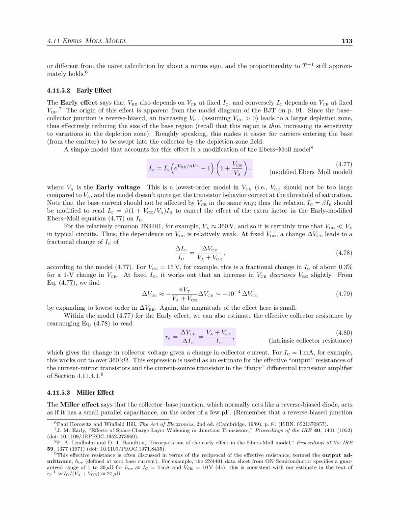
4.11 Ebers–Moll Model 113
or different from the naïve calculation by about a minus sign, and the proportionality to T −1 still approxi-mately holds.6
4.11.5.2 Early Effect
The Early effect says that VBE also depends on VCE at fixed IC, and conversely IC depends on VCE at fixedVBE.7 The origin of this effect is apparent from the model diagram of the BJT on p. 91. Since the base–collector junction is reverse-biased, an increasing VCE (assuming VCE > 0) leads to a larger depletion zone,thus effectively reducing the size of the base region (recall that this region is thin, increasing its sensitivityto variations in the depletion zone). Roughly speaking, this makes it easier for carriers entering the base(from the emitter) to be swept into the collector by the depletion-zone field.
A simple model that accounts for this effect is a modification of the Ebers–Moll model8
IC = IS
(
eVBE/nVT − 1)
(
1 +VCE
VA
)
,(4.77)
(modified Ebers–Moll model)
where VA is the Early voltage. This is a lowest-order model in VCE (i.e., VCE should not be too largecompared to VA, and the model doesn’t quite get the transistor behavior correct at the threshold of saturation.Note that the base current should not be affected by VCE in the same way; thus the relation IC = βIB shouldbe modified to read IC = β(1 + VCE/VA)IB to cancel the effect of the extra factor in the Early-modifiedEbers–Moll equation (4.77) on IB.
For the relatively common 2N4401, for example, VA ≈ 360 V, and so it is certainly true that VCE ≪ VA
in typical circuits. Thus, the dependence on VCE is relatively weak. At fixed VBE, a change ∆VCE leads to afractional change of IC of
∆IC
IC
=∆VCE
VA + VCE
, (4.78)
according to the model (4.77). For VCE = 15 V, for example, this is a fractional change in IC of about 0.3%for a 1-V change in VCE. At fixed IC, it works out that an increase in VCE decreases VBE slightly. FromEq. (4.77), we find
∆VBE ≈ −nVT
VA + VCE
∆VCE ∼ −10−4 ∆VCE (4.79)
by expanding to lowest order in ∆VBE. Again, the magnitude of the effect here is small.Within the model (4.77) for the Early effect, we can also estimate the effective collector resistance by
rearranging Eq. (4.78) to read
rc =∆VCE
∆IC
=VA + VCE
IC
,(4.80)
(intrinsic collector resistance)
which gives the change in collector voltage given a change in collector current. For IC = 1 mA, for example,this works out to over 360 kΩ. This expression is useful as an estimate for the effective “output” resistances ofthe current-mirror transistors and the current-source transistor in the “fancy” differential transistor amplifierof Section 4.11.4.1.9
4.11.5.3 Miller Effect
The Miller effect says that the collector–base junction, which normally acts like a reverse-biased diode, actsas if it has a small parallel capacitance, on the order of a few pF. (Remember that a reverse-biased junction
6Paul Horowitz and Winfield Hill, The Art of Electronics, 2nd ed. (Cambridge, 1989), p. 81 (ISBN: 0521370957).7J. M. Early, “Effects of Space-Charge Layer Widening in Junction Transistors,” Proceedings of the IRE 40, 1401 (1952)
(doi: 10.1109/JRPROC.1952.273969).8F. A. Lindholm and D. J. Hamilton, “Incorporation of the early effect in the Ebers-Moll model,” Proceedings of the IRE
59, 1377 (1971) (doi: 10.1109/PROC.1971.8435).9This effective resistance is often discussed in terms of the reciprocal of the effective resistance, termed the output ad-
mittance, hoe (defined at zero base current). For example, the 2N4401 data sheet from ON Semiconductor specifies a guar-anteed range of 1 to 30 µ for hoe at IC = 1 mA and VCE = 10 V (dc); this is consistent with our estimate in the text ofr−1
c ≈ IC/(VA + VCE) ≈ 27 µ.
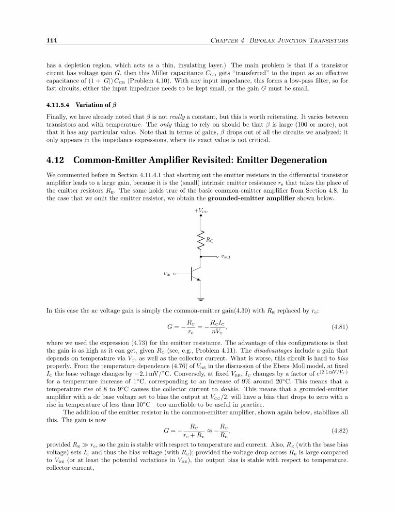
114 Chapter 4. Bipolar Junction Transistors
has a depletion region, which acts as a thin, insulating layer.) The main problem is that if a transistorcircuit has voltage gain G, then this Miller capacitance CCB gets “transferred” to the input as an effectivecapacitance of (1 + |G|) CCB (Problem 4.10). With any input impedance, this forms a low-pass filter, so forfast circuits, either the input impedance needs to be kept small, or the gain G must be small.
4.11.5.4 Variation of β
Finally, we have already noted that β is not really a constant, but this is worth reiterating. It varies betweentransistors and with temperature. The only thing to rely on should be that β is large (100 or more), notthat it has any particular value. Note that in terms of gains, β drops out of all the circuits we analyzed; itonly appears in the impedance expressions, where its exact value is not critical.
4.12 Common-Emitter Amplifier Revisited: Emitter Degeneration
We commented before in Section 4.11.4.1 that shorting out the emitter resistors in the differential transistoramplifier leads to a large gain, because it is the (small) intrinsic emitter resistance re that takes the place ofthe emitter resistors RE. The same holds true of the basic common-emitter amplifier from Section 4.8. Inthe case that we omit the emitter resistor, we obtain the grounded-emitter amplifier shown below.
vin
RC
+VCC
vout
In this case the ac voltage gain is simply the common-emitter gain(4.30) with RE replaced by re:
G = −RC
re= −RCIC
nVT
, (4.81)
where we used the expression (4.73) for the emitter resistance. The advantage of this configurations is thatthe gain is as high as it can get, given RC (see, e.g., Problem 4.11). The disadvantages include a gain thatdepends on temperature via VT, as well as the collector current. What is worse, this circuit is hard to bias
properly. From the temperature dependence (4.76) of VBE in the discussion of the Ebers–Moll model, at fixedIC the base voltage changes by −2.1 mV/C. Conversely, at fixed VBE, IC changes by a factor of e(2.1 mV/VT)
for a temperature increase of 1C, corresponding to an increase of 9% around 20C. This means that atemperature rise of 8 to 9C causes the collector current to double. This means that a grounded-emitteramplifier with a dc base voltage set to bias the output at VCC/2, will have a bias that drops to zero with arise in temperature of less than 10C—too unreliable to be useful in practice.
The addition of the emitter resistor in the common-emitter amplifier, shown again below, stabilizes allthis. The gain is now
G = − RC
re + RE
≈ −RC
RE
, (4.82)
provided RE ≫ re, so the gain is stable with respect to temperature and current. Also, RE (with the base biasvoltage) sets IC and thus the bias voltage (with RE); provided the voltage drop across RE is large comparedto VBE (or at least the potential variations in VBE), the output bias is stable with respect to temperature.collector current,
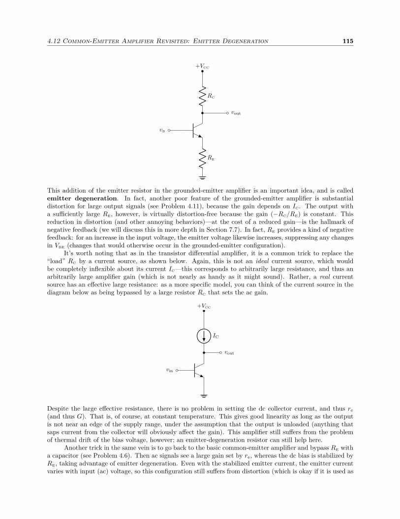
4.12 Common-Emitter Amplifier Revisited: Emitter Degeneration 115
vB
RE
RC
+VCC
vout
This addition of the emitter resistor in the grounded-emitter amplifier is an important idea, and is calledemitter degeneration. In fact, another poor feature of the grounded-emitter amplifier is substantialdistortion for large output signals (see Problem 4.11), because the gain depends on IC. The output witha sufficiently large RE, however, is virtually distortion-free because the gain (−RC/RE) is constant. Thisreduction in distortion (and other annoying behaviors)—at the cost of a reduced gain—is the hallmark ofnegative feedback (we will discuss this in more depth in Section 7.7). In fact, RE provides a kind of negativefeedback: for an increase in the input voltage, the emitter voltage likewise increases, suppressing any changesin VBE (changes that would otherwise occur in the grounded-emitter configuration).
It’s worth noting that as in the transistor differential amplifier, it is a common trick to replace the“load” RC by a current source, as shown below. Again, this is not an ideal current source, which wouldbe completely inflexible about its current IC—this corresponds to arbitrarily large resistance, and thus anarbitrarily large amplifier gain (which is not nearly as handy as it might sound). Rather, a real currentsource has an effective large resistance: as a more specific model, you can think of the current source in thediagram below as being bypassed by a large resistor RC that sets the ac gain.
vin
IC
+VCC
vout
Despite the large effective resistance, there is no problem in setting the dc collector current, and thus re
(and thus G). That is, of course, at constant temperature. This gives good linearity as long as the outputis not near an edge of the supply range, under the assumption that the output is unloaded (anything thatsaps current from the collector will obviously affect the gain). This amplifier still suffers from the problemof thermal drift of the bias voltage, however; an emitter-degeneration resistor can still help here.
Another trick in the same vein is to go back to the basic common-emitter amplifier and bypass RE witha capacitor (see Problem 4.6). Then ac signals see a large gain set by re, whereas the dc bias is stabilized byRE, taking advantage of emitter degeneration. Even with the stabilized emitter current, the emitter currentvaries with input (ac) voltage, so this configuration still suffers from distortion (which is okay if it is used as

116 Chapter 4. Bipolar Junction Transistors
a high-gain amplifier within a negative-feedback loop). When improved linearity via emitter degeneration isstill desirable at ac frequencies, the circuit below is a common amplifier.
vB
RE
RC
+VCC
vout
C
R′E
At ac frequencies the emitter resistance is RE‖R′E
(which is just R′E
if R′E≪ RE). This circuit allows
the amount of emitter degeneration to be set independently at ac and dc by choosing the two resistorsappropriately.
4.13 Biasing the Push–Pull Pair
The single-transistor amplifiers that we have studied so far have required a dc bias to keep the desired acsignal away from the lower power supply. In high-power circuits, this is typically a bad thing: the quiescent(dc) current, which is flowing even when there is no ac signal, wastes a lot of power. Thus a high-poweremitter follower is typically not a good idea (not without a huge heatsink, anyway).
One attempt to improve this is to stack a complementary pair of emitter followers, in a push–pullcurrent amplifier, as shown below.
Vin Vout
+VCC
−VEE
The idea is that, when Vout is connected to ground via a load, the NPN transistor conducts when Vin > 0, andthe PNP takes over when Vin < 0. The basic problem with this circuit is that to make one of the transistorsconduct, the emitter (output) voltage must be a diode drop closer to ground than the base (input) voltage.That is, a graph of the output voltage responding to input voltage looks schematically as in the graph below,if we assume the simple model that the forward-biased base–emitter voltage drop is 0.6 V.

4.13 Biasing the Push–Pull Pair 117
Vout
Vin0.6 V-0.6 V
The problem in using this as an amplifier is that it leads to crossover distortion, because the base-emitterdrop changes as the signal crosses through zero. If you put a relatively large (compared to 0.6 V) sine waveinto the input, the output shows the crossover distortion whenever the signal is crossing through zero.
V
t
VinVinVin
Vout
Yeesh, that’s not good.One solution to this problem is to “bias” the transistor bases into conduction: basically, boost the
NPN’s base by 0.6 V, and “unboost” the PNP’s base by −0.6 V. Then with a 0-V input, both transistorsare just at the edge of conduction, but in opposition so their currents cancel. This wastes a bit of power atidle, but largely removes the problem with crossover distortion. The uncorrected amplifier is called a class-B amplifier, while the bias-corrected amplifier is called a class-AB amplifier (the less-efficient emitterfollower is a class-A amplifier.
One method of biasing the push–pull pair is to use a voltage divider to generate the ±0.6-V bias points.Variable resistances can allow the bias points to be fine-tuned. Another common technique is to generatethe bias voltages that match the base–emitter bias junctions using another pair of junctions, such as diodes.The basic scheme is shown below.
Vin Vout
+VCC
−VEE
The forward-biased diodes act as part of a stiff voltage divider that set the appropriate bias points; thechoice of resistors will affect the impedance seen by the signal source at the input (these could be replaced

118 Chapter 4. Bipolar Junction Transistors
by current sources to have high effective input impedance while selecting the proper current to match thetransistor VBE’s). A common variation on the above idea is to use matching biasing transistors in place ofthe diodes, as shown below.
Vin Vout
+VCC
−VEE
This better matches the bias voltages to the base–emitter drops, but is probably only practical for signal-levelcircuits (this is a common trick in the internals of an op-amp, for example).
The one remaining problem is the temperature stability of the bias in high-current applications. Theoutput power transistors heat up as they deliver power to the load; this causes their VBE’s to drop. If thelow-power bias diodes are thermally decoupled from the power transistors, the fixed bias voltage causesthe quiescent current to increase, just as we saw in the grounded-emitter amplifier in Section 4.12. Thiscan lead to thermal runaway, where the increased quiescent current leads to more heating, which leadsto yet more quiescent current, and so on. The solution, as in the grounded-emitter amplifier, is to addemitter-degeneration resistors, as shown below.

4.14 Mathematical Modeling of DC BJT Behavior 119
Vin Vout
+VCC
−VEE
This increases the voltage drop from the transistor bases to Vout—the idea is that the voltage drop acrossthe (relatively small) emitter resistors should be large compared to the anticipated change in VBE due totemperature changes (i.e., larger than ∼100 mV, but not too much larger). Extra (small) resistors have alsobeen added to correspondingly boost the bias voltages in the diode chain; adjustable resistors here are usefulin setting the quiescent current (which should be something bigger than zero so that both transistors are inslight conduction, ready to “take over” the signal when it crosses through zero).
4.14 Mathematical Modeling of DC BJT Behavior
The basic design equations that we have used so far are the basic Ebers–Moll model (4.60), along with thecurrent-gain equation:
IC = IS
(
eVBE/nVT − 1)
IB = IC/β.(4.83)
We have also inserted some rough voltage drops as appropriate, such as VBE ≈ 0.6 V when the base is forward-biased with respect to the emitter, and VCE ≈ 0.2 V in saturation. Here we will briefly discuss more detailedmathematical modeling of the transistors, and as a by-product discuss the BJT “characteristic curves” thatare used in diagnosis and characterization of transistors, and were in the past used for graphical design oftransistor circuits.
4.14.1 Ebers–Moll Model
The main issue with the model equations (4.83) are that they are too simplistic for certain circumstances.For example, they predict that IC is completely independent of VCE, so they cannot correctly handle anysaturation behavior (without inserting a saturation voltage by hand). However, the same diode-law treatmentof the base–emitter junction applies to the other junctions, so we can write the more detailed Ebers–Moll
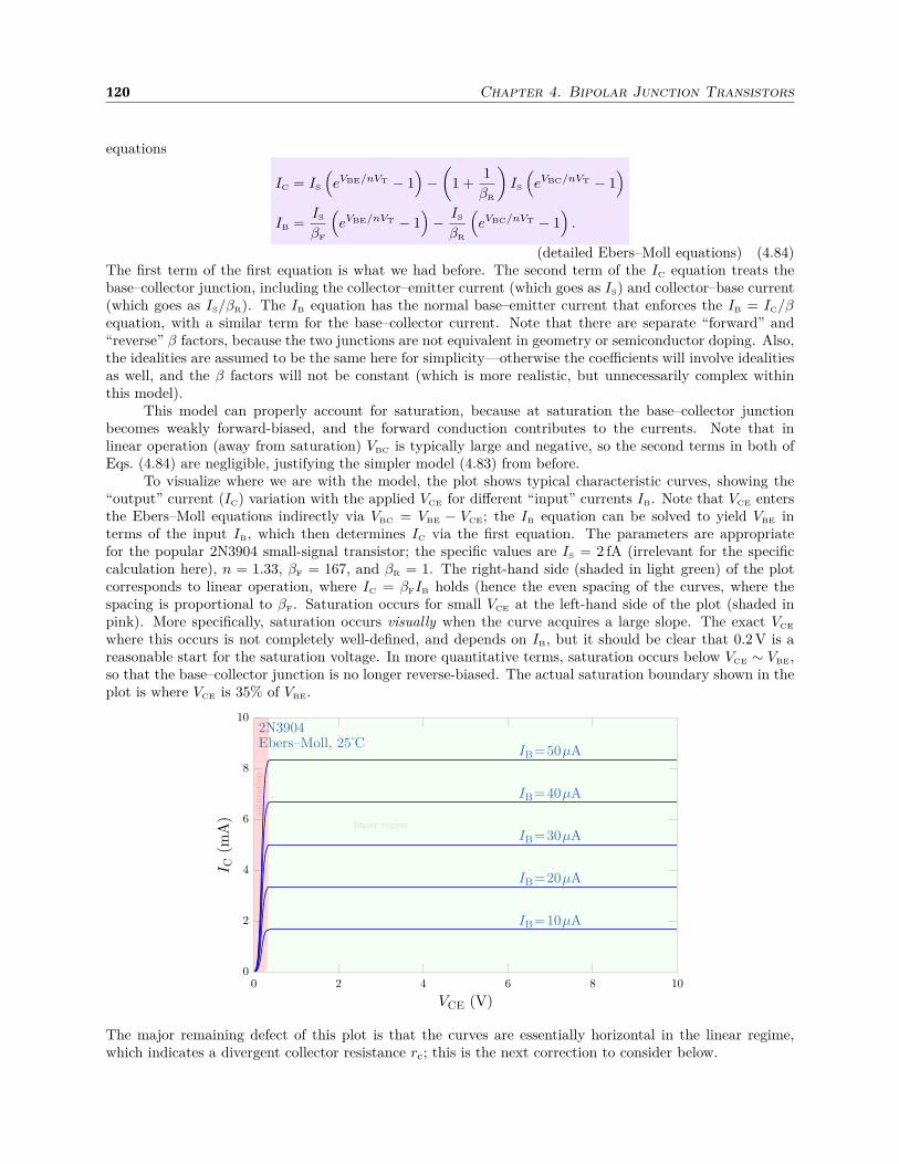
120 Chapter 4. Bipolar Junction Transistors
equations
IC = IS
(
eVBE/nVT − 1)
−(
1 +1
βR
)
IS
(
eVBC/nVT − 1)
IB =IS
βF
(
eVBE/nVT − 1)
− IS
βR
(
eVBC/nVT − 1)
.
(detailed Ebers–Moll equations) (4.84)The first term of the first equation is what we had before. The second term of the IC equation treats thebase–collector junction, including the collector–emitter current (which goes as IS) and collector–base current(which goes as IS/βR). The IB equation has the normal base–emitter current that enforces the IB = IC/βequation, with a similar term for the base–collector current. Note that there are separate “forward” and“reverse” β factors, because the two junctions are not equivalent in geometry or semiconductor doping. Also,the idealities are assumed to be the same here for simplicity—otherwise the coefficients will involve idealitiesas well, and the β factors will not be constant (which is more realistic, but unnecessarily complex withinthis model).
This model can properly account for saturation, because at saturation the base–collector junctionbecomes weakly forward-biased, and the forward conduction contributes to the currents. Note that inlinear operation (away from saturation) VBC is typically large and negative, so the second terms in both ofEqs. (4.84) are negligible, justifying the simpler model (4.83) from before.
To visualize where we are with the model, the plot shows typical characteristic curves, showing the“output” current (IC) variation with the applied VCE for different “input” currents IB. Note that VCE entersthe Ebers–Moll equations indirectly via VBC = VBE − VCE; the IB equation can be solved to yield VBE interms of the input IB, which then determines IC via the first equation. The parameters are appropriatefor the popular 2N3904 small-signal transistor; the specific values are IS = 2 fA (irrelevant for the specificcalculation here), n = 1.33, βF = 167, and βR = 1. The right-hand side (shaded in light green) of the plotcorresponds to linear operation, where IC = βFIB holds (hence the even spacing of the curves, where thespacing is proportional to βF. Saturation occurs for small VCE at the left-hand side of the plot (shaded inpink). More specifically, saturation occurs visually when the curve acquires a large slope. The exact VCE
where this occurs is not completely well-defined, and depends on IB, but it should be clear that 0.2 V is areasonable start for the saturation voltage. In more quantitative terms, saturation occurs below VCE ∼ VBE,so that the base–collector junction is no longer reverse-biased. The actual saturation boundary shown in theplot is where VCE is 35% of VBE.
satu
rati
on
linear region
VCE (V)0 102 4 6 8
IC (
mA
)
10
0
2
4
6
8
IBo=o10omA
IBo=o20omA
IBo=o30omA
IBo=o40omA
IBo=o50omA
2N3904Ebers–Moll, 25 C
The major remaining defect of this plot is that the curves are essentially horizontal in the linear regime,which indicates a divergent collector resistance rc; this is the next correction to consider below.
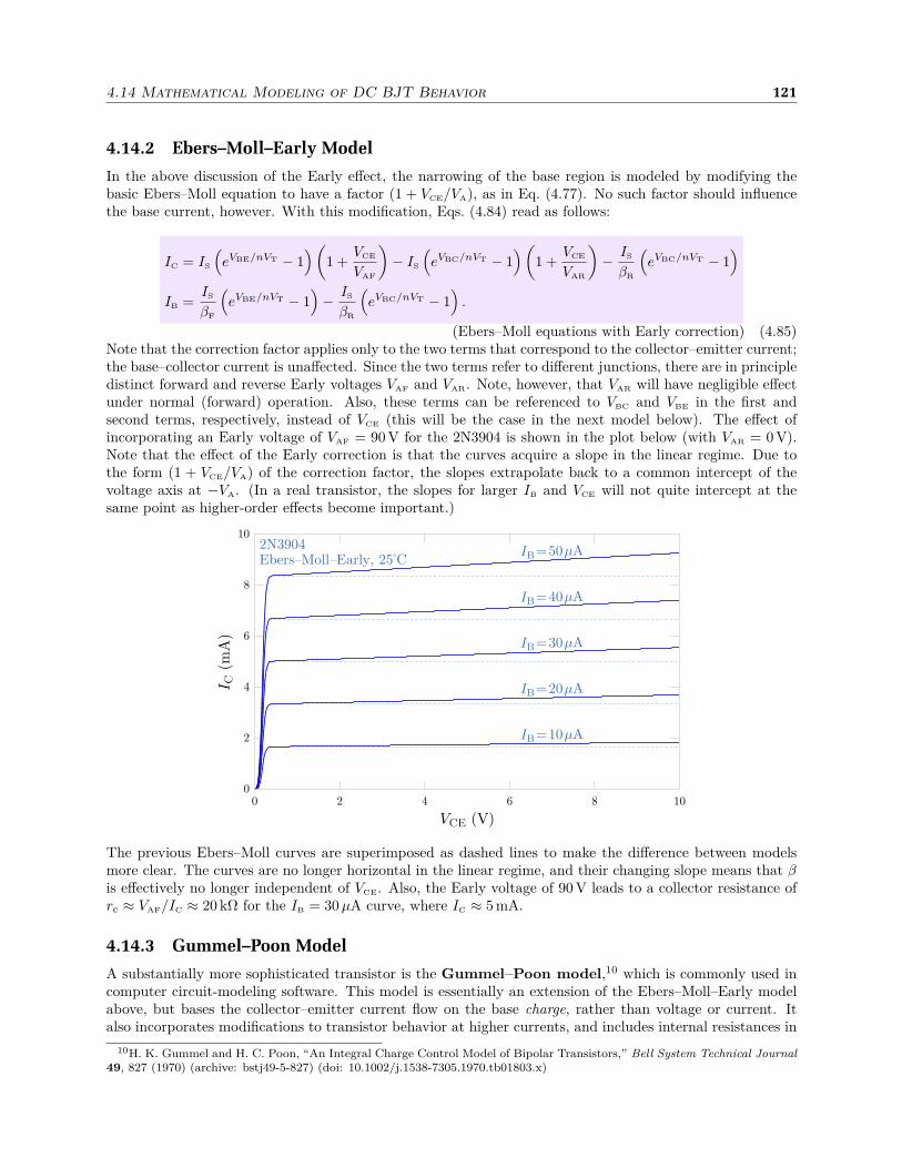
4.14 Mathematical Modeling of DC BJT Behavior 121
4.14.2 Ebers–Moll–Early Model
In the above discussion of the Early effect, the narrowing of the base region is modeled by modifying thebasic Ebers–Moll equation to have a factor (1 + VCE/VA), as in Eq. (4.77). No such factor should influencethe base current, however. With this modification, Eqs. (4.84) read as follows:
IC = IS
(
eVBE/nVT − 1)
(
1 +VCE
VAF
)
− IS
(
eVBC/nVT − 1)
(
1 +VCE
VAR
)
− IS
βR
(
eVBC/nVT − 1)
IB =IS
βF
(
eVBE/nVT − 1)
− IS
βR
(
eVBC/nVT − 1)
.
(Ebers–Moll equations with Early correction) (4.85)Note that the correction factor applies only to the two terms that correspond to the collector–emitter current;the base–collector current is unaffected. Since the two terms refer to different junctions, there are in principledistinct forward and reverse Early voltages VAF and VAR. Note, however, that VAR will have negligible effectunder normal (forward) operation. Also, these terms can be referenced to VBC and VBE in the first andsecond terms, respectively, instead of VCE (this will be the case in the next model below). The effect ofincorporating an Early voltage of VAF = 90 V for the 2N3904 is shown in the plot below (with VAR = 0 V).Note that the effect of the Early correction is that the curves acquire a slope in the linear regime. Due tothe form (1 + VCE/VA) of the correction factor, the slopes extrapolate back to a common intercept of thevoltage axis at −VA. (In a real transistor, the slopes for larger IB and VCE will not quite intercept at thesame point as higher-order effects become important.)
VCE (V)0 102 4 6 8
IC (
mA
)
10
0
2
4
6
8
IBo=o10omA
IBo=o20omA
IBo=o30omA
IBo=o40omA
IBo=o50omA2N3904Ebers–Moll–Early, 25 C
The previous Ebers–Moll curves are superimposed as dashed lines to make the difference between modelsmore clear. The curves are no longer horizontal in the linear regime, and their changing slope means that βis effectively no longer independent of VCE. Also, the Early voltage of 90 V leads to a collector resistance ofrc ≈ VAF/IC ≈ 20 kΩ for the IB = 30 µA curve, where IC ≈ 5 mA.
4.14.3 Gummel–Poon Model
A substantially more sophisticated transistor is the Gummel–Poon model,10 which is commonly used incomputer circuit-modeling software. This model is essentially an extension of the Ebers–Moll–Early modelabove, but bases the collector–emitter current flow on the base charge, rather than voltage or current. Italso incorporates modifications to transistor behavior at higher currents, and includes internal resistances in
10H. K. Gummel and H. C. Poon, “An Integral Charge Control Model of Bipolar Transistors,” Bell System Technical Journal49, 827 (1970) (archive: bstj49-5-827) (doi: 10.1002/j.1538-7305.1970.tb01803.x)
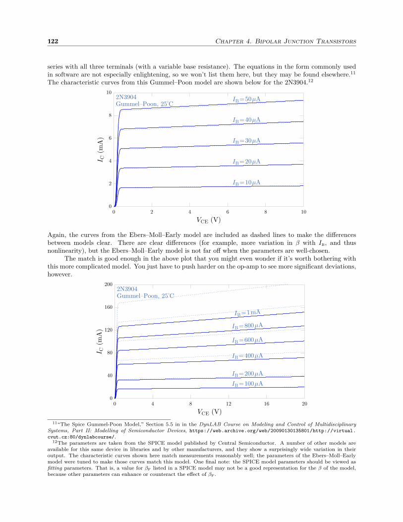
122 Chapter 4. Bipolar Junction Transistors
series with all three terminals (with a variable base resistance). The equations in the form commonly usedin software are not especially enlightening, so we won’t list them here, but they may be found elsewhere.11
The characteristic curves from this Gummel–Poon model are shown below for the 2N3904.12
VCE (V)0 102 4 6 8
IC (
mA
)10
0
2
4
6
8
IBo=o10omA
IBo=o20omA
IBo=o30omA
IBo=o40omA
IBo=o50omA2N3904Gummel–Poon, 25 C
Again, the curves from the Ebers–Moll–Early model are included as dashed lines to make the differencesbetween models clear. There are clear differences (for example, more variation in β with IB, and thusnonlinearity), but the Ebers–Moll–Early model is not far off when the parameters are well-chosen.
The match is good enough in the above plot that you might even wonder if it’s worth bothering withthis more complicated model. You just have to push harder on the op-amp to see more significant deviations,however.
VCE (V)0 204 8 12 16
IC (
mA
)
200
0
40
80
120
160
IBo=o100omA
IBo=o200omA
IBo=o400omA
IBo=o600omA
IBo=o800omA
IBo=o1omA
2N3904Gummel–Poon, 25 C
11“The Spice Gummel-Poon Model,” Section 5.5 in in the DynLAB Course on Modeling and Control of MultidisciplinarySystems, Part II: Modelling of Semiconductor Devices, https://web.archive.org/web/20090130135801/http://virtual.
cvut.cz:80/dynlabcourse/.12The parameters are taken from the SPICE model published by Central Semiconductor. A number of other models are
available for this same device in libraries and by other manufacturers, and they show a surprisingly wide variation in theiroutput. The characteristic curves shown here match measurements reasonably well; the parameters of the Ebers–Moll–Earlymodel were tuned to make those curves match this model. One final note: the SPICE model parameters should be viewed asfitting parameters. That is, a value for βF listed in a SPICE model may not be a good representation for the β of the model,because other parameters can enhance or counteract the effect of βF.
4.15 Little-“h” Notation 123
This plot is getting closer to the limits of this transistor, which is rated for a maximum IC of 200 mA, anda maximum VCE of 40 V (at IB = 0). One physical feature still typically missing from the more completemodels is breakdown at high VCE (and reverse breakdown), but this is not a big issue provided you respectthe device limits published in the data sheet!
4.15 Little-“h” Notation
In the development of the BJT here, we have stuck to a few relatively simple parameters, such as β, maybean Early voltage, and of course the various input and output currents and voltages. We have also brieflymentioned a couple of other parameters, like hFE and hfe (p. 93), and hoe (Section 4.11.5.2). This notationis widespread in transistor data sheets, and so it’s worth explaining this briefly.
The idea is that for any of the basic transistor-amplifier circuits that we have studied, there is areinput and output voltages, as well as input and output currents. Mostly we have stuck to relating input andoutput voltages, but the currents can also influence or be caused by the voltages. Suppose we consider verygenerally how Vin, Iin, Vout, and Iout are interrelated. For not-very-obvious reasons it is conventional to takeIin and Vout as given, and the other variables to be functions of these:
Vin = Vin(Iin, Vout)
Iout = Iout(Iin, Vout).(4.86)
Considering small variations ∆Vin and ∆Iout of the “outputs” due to small variations δIin and δVout of the“inputs” gives, by the chain rule,
∆Vin =∂Vin
∂Iin∆Iin +
∂Vin
∂Vout∆Vout
∆Iout =∂Iout
∂Iin∆Iin +
∂Iout
∂Vout∆Vout.
(4.87)
It is then conventional to represent the partial derivatives with “constants” with labels of the form hxy.The “h” comes from this being the “hybrid model” of the transistor. The different possible values for the ysubscript are:
• e: for the common-emitter amplifier (Section 4.8); this is the option most commonly found in datasheets.
• c: for the common-collector amplifier (i.e., the emitter follower, Section 4.6)
• b: for the common-base amplifier (see Problem 4.3)
The basic idea is that a BJT has three terminals; one will act as an input, another an output, and the thirda common voltage reference for the other two (i.e., ground). This leaves three sensible options for transistorconfigurations, corresponding to grounding one of each of three terminals (the input and output are fixedby requiring that the transistor have some amplifying action).
The first subscript x then takes on four different values to denote one of the partial derivatives inEqs. (4.87);
• i: for the input impedance ∂Vin/∂Iin
• r: for the reverse voltage ratio or voltage feedback ratio ∂Vin/∂Vout
• f: for the forward current ratio or small-signal current gain ∂Iout/∂Iin
• o: for the output admittance ∂Iout/∂Vout

124 Chapter 4. Bipolar Junction Transistors
Thus, for a common-emitter amplifier, Eqs. (4.87) become
vin = hieiin + hrevout
iout = hfeiin + hoevout,
(hybrid-model equations, common-emitter configuration) (4.88)if we use ac notation for the changes in voltage and current instead of the “delta” notation of Eqs. (4.87).For the common-emitter amplifier, iin = iB and iout = iC: the “output current” of the amplifier is thecurrent flowing into the “output,” which is the collector, as shown below. (Note that since these parameterscharacterize only the transistor, the reference circuit omits any external resistances, but we assume it to bebiased properly to work as an amplifier.)
iout
iin
vin
vout
Thus, the second equation is just the transistor law if we identify β = hfe (recall that the second term is anEarly-effect correction due to vCE, which is small because the collector’s intrinsic resistance rc is large).
The lower-case subscripts indicate that these are ac quantities (i.e., they refer to partial derivatives atsome nonzero bias values of Iin and Vout). These are sometimes reported as dc quantities, in which case thesubscripts are written in upper cases. The analogous relations to Eqs. (4.88) for the dc case would then be
Vin = hIEIin + hREVout
Iout = hFEIin + hOEVout.(4.89)
For our purposes, we have been referring to both hFE and hfe interchangeably as β, although they are notthe same.
To give some sense of typical values, for the 2N4401,13 at a (dc) bias current IC = 1 mA, VCE = 10 V,and a signal frequency of 1 kHz, the guaranteed range of each parameter is listed below.
parameter min value max value
hie (input impedance) 1 kΩ 15 kΩ
hre (reverse voltage ratio) 10−5 8× 10⁻⁴
hfe (forward current gain) 40 500
hoe (output admittance) 1 µ 30 µ
Note that the intrinsic emitter resistance re is a useful parameter that doesn’t appear among these param-eters. However, in the common-emitter configuration, you can view the input impedance as the emitterresistance, but amplified by roughly a factor of β [Eq. (4.12)]. Thus, we can estimate re based on the aboveparameters via hie ≈ hfere. Taking typical values (“unit 1” from the data-sheet plots) of hfe ≈ 200 andhie ≈ 5.5 kΩ, this gives re ≈ 28 Ω at IC = 1 mA. This agrees with the prediction of re = nVT/IC ≈ 28.3 Ωfrom the Ebers–Moll model (at 25C and assuming n = 1.1).
4.16 Circuit Practice
4.16.1 Transistor Switching an Inductive Load
Consider the circuit below, where an NPN transistor switches an inductive load (electromagnet, motor, etc.).
13as specified by ON Semiconductor, http://www.onsemi.com/pub/Collateral/2N4401-D.PDF
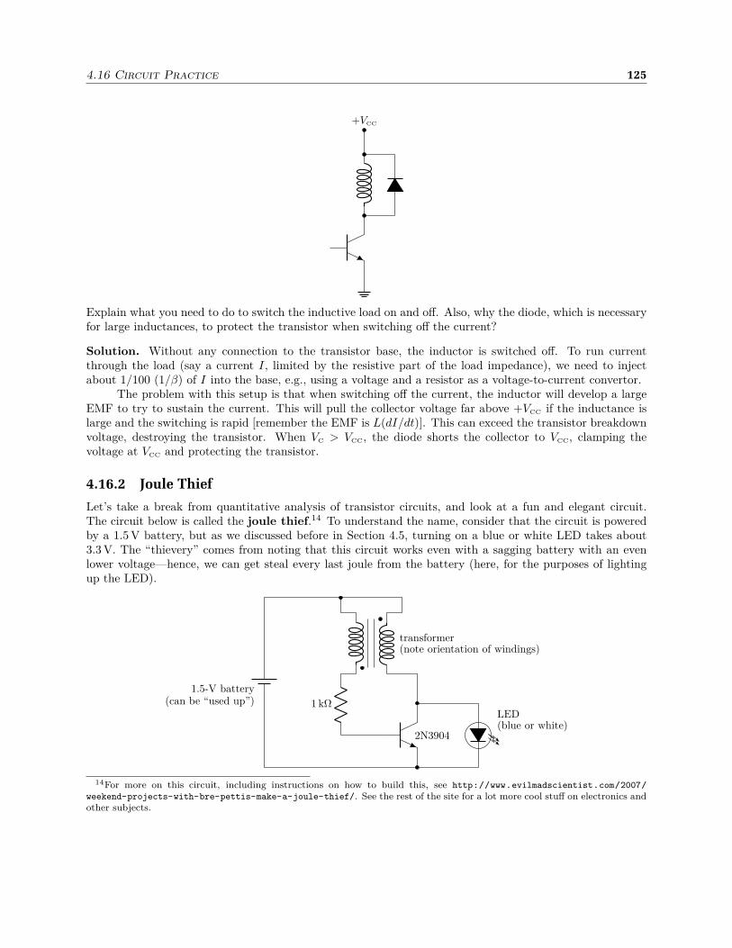
4.16 Circuit Practice 125
+VCC
Explain what you need to do to switch the inductive load on and off. Also, why the diode, which is necessaryfor large inductances, to protect the transistor when switching off the current?
Solution. Without any connection to the transistor base, the inductor is switched off. To run currentthrough the load (say a current I, limited by the resistive part of the load impedance), we need to injectabout 1/100 (1/β) of I into the base, e.g., using a voltage and a resistor as a voltage-to-current convertor.
The problem with this setup is that when switching off the current, the inductor will develop a largeEMF to try to sustain the current. This will pull the collector voltage far above +VCC if the inductance islarge and the switching is rapid [remember the EMF is L(dI/dt)]. This can exceed the transistor breakdownvoltage, destroying the transistor. When VC > VCC, the diode shorts the collector to VCC, clamping thevoltage at VCC and protecting the transistor.
4.16.2 Joule Thief
Let’s take a break from quantitative analysis of transistor circuits, and look at a fun and elegant circuit.The circuit below is called the joule thief.14 To understand the name, consider that the circuit is poweredby a 1.5 V battery, but as we discussed before in Section 4.5, turning on a blue or white LED takes about3.3 V. The “thievery” comes from noting that this circuit works even with a sagging battery with an evenlower voltage—hence, we can get steal every last joule from the battery (here, for the purposes of lightingup the LED).
2N3904
1 kΩLED(blue or white)
1.5-V battery(can be “used up”)
transformer(note orientation of windings)
14For more on this circuit, including instructions on how to build this, see http://www.evilmadscientist.com/2007/
weekend-projects-with-bre-pettis-make-a-joule-thief/. See the rest of the site for a lot more cool stuff on electronics andother subjects.

126 Chapter 4. Bipolar Junction Transistors
Your exercise here is to trace through the circuit and explain how it works. Just treat the transistor as aswitch; no need to do any calculations. Also, as a hint, note that inductors are fairly rare in circuits; usuallythey show up either as filters (as in the outputs of switching power supplies for computers), or—as is thecase here—they are around to give an inductive kick when they are interrupted (like the spark-plug coil ingasoline-powered car engines).
Solution. Suppose we start with the transistor off. Current starts flowing from the battery, but it can’tgo into the collector. The only path it has is into the base; the resistor is there to make sure we don’toverdo the current. This base current turns on the transistor, so a much larger current can start to flow intothe collector. As the current flows through the secondary of the transformer to the collector, the opposite
current is induced in the primary (note the primary and secondary are wound/oriented oppositely). Thisinduced current opposes and thus interrupts the base current, switching off the transistor. This interruptsthe collector current, interrupting the relatively large current in the transformer secondary. This leads toan inductive kick, and the collector voltage builds up potentially far above the battery voltage (recall thesame thing happens for a transistor switching off an inductive load, as in Section 4.16.1). The collector thusbuilds up to a sufficiently high voltage that the LED turns on, dumping the inductive kick. Then we areback to the initial state, and the process repeats.
4.16.3 Solid-State Tesla Coil
Here is another good circuit to practice qualitative reading of transistor operation.
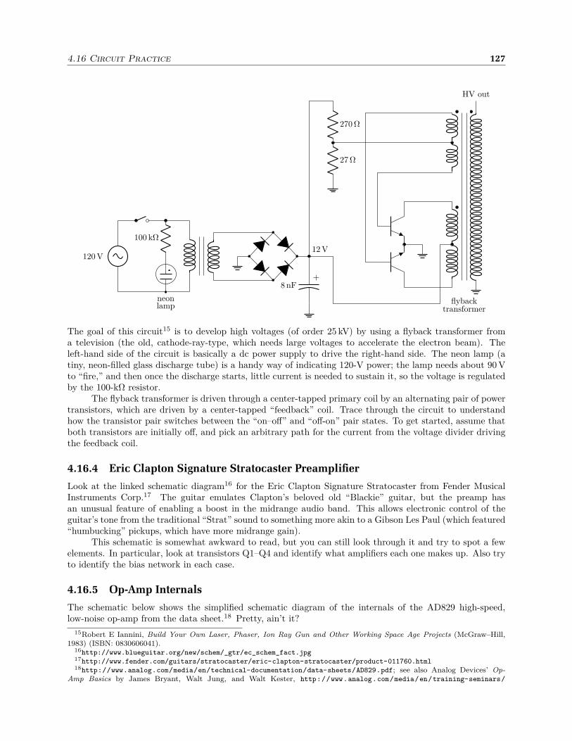
4.16 Circuit Practice 127
120 V
neonlamp
100 kΩ
8 nF+
HV out
flybacktransformer
12 V
270 Ω
27 Ω
The goal of this circuit15 is to develop high voltages (of order 25 kV) by using a flyback transformer froma television (the old, cathode-ray-type, which needs large voltages to accelerate the electron beam). Theleft-hand side of the circuit is basically a dc power supply to drive the right-hand side. The neon lamp (atiny, neon-filled glass discharge tube) is a handy way of indicating 120-V power; the lamp needs about 90 Vto “fire,” and then once the discharge starts, little current is needed to sustain it, so the voltage is regulatedby the 100-kΩ resistor.
The flyback transformer is driven through a center-tapped primary coil by an alternating pair of powertransistors, which are driven by a center-tapped “feedback” coil. Trace through the circuit to understandhow the transistor pair switches between the “on–off” and “off-on” pair states. To get started, assume thatboth transistors are initially off, and pick an arbitrary path for the current from the voltage divider drivingthe feedback coil.
4.16.4 Eric Clapton Signature Stratocaster Preamplifier
Look at the linked schematic diagram16 for the Eric Clapton Signature Stratocaster from Fender MusicalInstruments Corp.17 The guitar emulates Clapton’s beloved old “Blackie” guitar, but the preamp hasan unusual feature of enabling a boost in the midrange audio band. This allows electronic control of theguitar’s tone from the traditional “Strat” sound to something more akin to a Gibson Les Paul (which featured“humbucking” pickups, which have more midrange gain).
This schematic is somewhat awkward to read, but you can still look through it and try to spot a fewelements. In particular, look at transistors Q1–Q4 and identify what amplifiers each one makes up. Also tryto identify the bias network in each case.
4.16.5 Op-Amp Internals
The schematic below shows the simplified schematic diagram of the internals of the AD829 high-speed,low-noise op-amp from the data sheet.18 Pretty, ain’t it?
15Robert E Iannini, Build Your Own Laser, Phaser, Ion Ray Gun and Other Working Space Age Projects (McGraw–Hill,1983) (ISBN: 0830606041).
16http://www.blueguitar.org/new/schem/_gtr/ec_schem_fact.jpg17http://www.fender.com/guitars/stratocaster/eric-clapton-stratocaster/product-011760.html18http://www.analog.com/media/en/technical-documentation/data-sheets/AD829.pdf; see also Analog Devices’ Op-
Amp Basics by James Bryant, Walt Jung, and Walt Kester, http://www.analog.com/media/en/training-seminars/
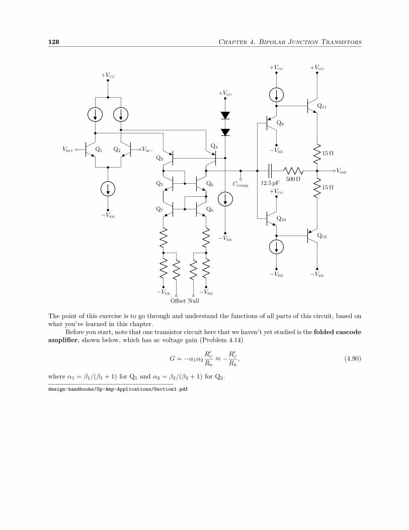
128 Chapter 4. Bipolar Junction Transistors
Q1 Q2Vin+ Vin−
−VEE
+VCC
Q5 Q6
Q7 Q8
Q3
Q4
−VEE −VEE
Offset Null
+VCC
−VEE
Q9
Q10
−VEE
+VCC
−VEE
+VCC
Ccomp
Q11
Q12
15 Ω
15 Ω12.5 pF
500 Ω
+VCC
−VEE
Vout
The point of this exercise is to go through and understand the functions of all parts of this circuit, based onwhat you’ve learned in this chapter.
Before you start, note that one transistor circuit here that we haven’t yet studied is the folded cascodeamplifier, shown below, which has ac voltage gain (Problem 4.14)
G = −α1α2R′
C
RE
≈ −R′C
RE
, (4.90)
where α1 = β1/(β1 + 1) for Q1 and α2 = β2/(β2 + 1) for Q2.
design-handbooks/Op-Amp-Applications/Section1.pdf

4.16 Circuit Practice 129
Q1 Q2
RC
+VCC
RE R′C
vout
vin Vbias
That is, this circuit behaves fairly similarly to the common-emitter amplifier, but with two transistors insteadof one (functioning something like a common-emitter amp cascaded with a common-base amp). The mainadvantages of this circuit are that it suppresses the Miller and Early effects.Solution. Q1 and Q2 form a transistor differential amplifier; the current source to −VEE acts as the “longtail,” or an effectively large REE, while the other two current sources appear to act as large RC resistances(the RE resistors are omitted for high gain based on the transistor re). But this is a little more complicated,because Q3 and Q4 are part of the differential amplifier two; the “transistors” involved in the differentialamplifier are actually folded-cascode amplifiers instead of common-emitter amplifiers as we originally learnedthe differential amplifier. The main benefit is probably the reduced Miller effect for high speed of the inputstage. The two-diode network in series with the current source is the bias circuit for the two cascode circuits(biased close to VCC to allow a wide swing voltage for the cascode outputs), and the “loads” of the cascodecircuits is the pair of current mirrors formed by Q5 with Q6 and Q7 with Q8. The current mirror is a goodload to replace RC resistors to obtain high gain in a differential amplifier, but here the mirror is the loadat the outputs of the of the folded-cascode circuits rather than the directly at the collectors of the inputtransistors. Why the stacked mirrors? Recall that there is some error in the current mirror associated withthe small base currents flowing through only one of the emitters; this trick of stacking two current mirrors inopposite senses cancels this base-current error, and is called an improved Wilson current mirror. Theresistors to −VEE provide some emitter degeneration increase the effective collector impedance at the output(the collector of Q6). Of course it also gives a method of trimming the balance of the current mirror usingthe offset-null pins (where a potentiometer with wiper connected to −VEE would be connected).
Now the output of the current mirror drives a push-pull output stage, with complementary outputpair Q11 and Q12. The output transistors have emitter-degeneration resistors for thermal stability. Q9 andQ10 function to bias the bases of the output transistors, but also serve as first-stage emitter followers (withhigh effective RE), so the output current is boosted in two stages (for good output current while minimizingloading effects on the current mirror; the data sheet specifies a current gain of 40 000 for the output stage).The Ccomp is a terminal for an external compensation capacitor (to ground), which can roll off the amplifiergain at high frequencies for stability. The remaining R–C pair is a little more complicated. Note that atlow frequencies, this capacitor is “bootstrapped”, meaning that the voltage on either side of the capacitorshould be the same, in which case the capacitor is irrelevant. At higher frequencies, when the output of thepush–pull stage lags the input (especially with a capacitive load connected), this R–C network provides a(negative) feedback path to the push–pull input, which effectively also rolls off the gain of this output stageat high frequencies (again, to help ensure stability).

130 Chapter 4. Bipolar Junction Transistors
4.17 Exercises
Problem 4.1
In the circuit below, for what range of resistances RC will the transistor be saturated?
+15 V
10 kΩ
RC
Assume β = 100.
Problem 4.2
Consider the following transistor circuit. Consider VCC, RB, and RC to be fixed. For what range ofinput voltage Vin is the transistor saturated?
RB
Vin
RC
+VCC
Problem 4.3
Consider the transistor circuit below. Assume the input is biased such that the transistor worksnormally, and ignore any internal resistances in the transistor. For the calculations in this problem,you may assume β ≫ 1.
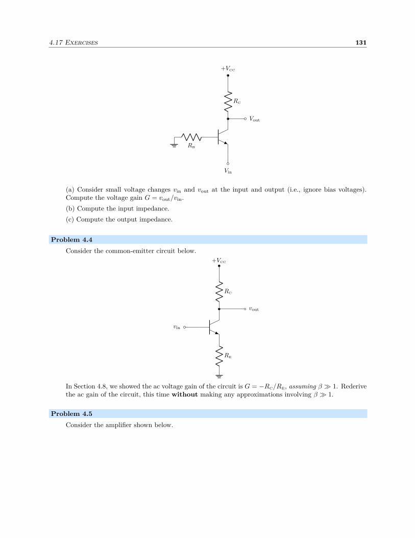
4.17 Exercises 131
RB
+VCC
Vin
RC
Vout
(a) Consider small voltage changes vin and vout at the input and output (i.e., ignore bias voltages).Compute the voltage gain G = vout/vin.
(b) Compute the input impedance.
(c) Compute the output impedance.
Problem 4.4
Consider the common-emitter circuit below.
vin
RE
RC
+VCC
vout
In Section 4.8, we showed the ac voltage gain of the circuit is G = −RC/RE, assuming β ≫ 1. Rederivethe ac gain of the circuit, this time without making any approximations involving β ≫ 1.
Problem 4.5
Consider the amplifier shown below.
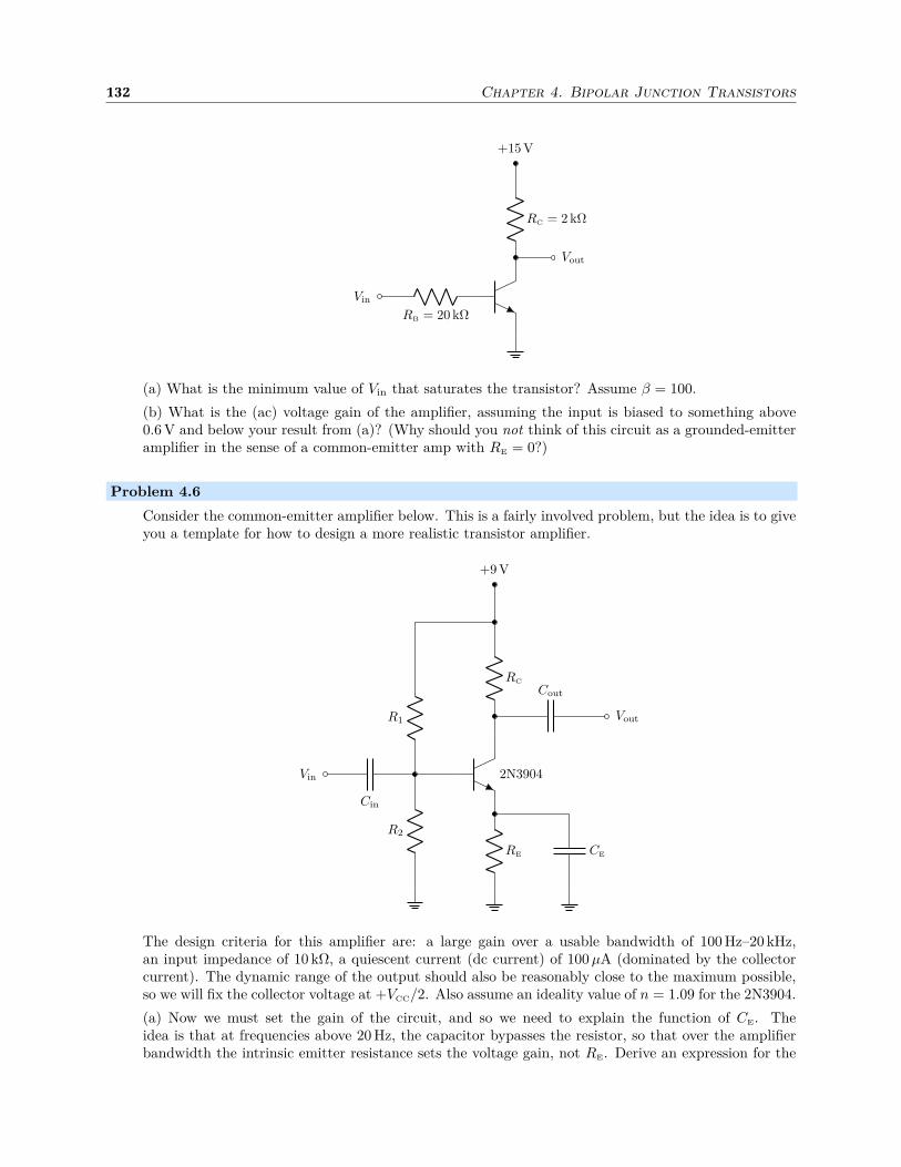
132 Chapter 4. Bipolar Junction Transistors
RB = 20 kΩ
Vin
RC = 2 kΩ
+15 V
Vout
(a) What is the minimum value of Vin that saturates the transistor? Assume β = 100.
(b) What is the (ac) voltage gain of the amplifier, assuming the input is biased to something above0.6 V and below your result from (a)? (Why should you not think of this circuit as a grounded-emitteramplifier in the sense of a common-emitter amp with RE = 0?)
Problem 4.6
Consider the common-emitter amplifier below. This is a fairly involved problem, but the idea is to giveyou a template for how to design a more realistic transistor amplifier.
2N3904
Cin
Vin
R1
R2
Cout
Vout
RE CE
RC
+9 V
The design criteria for this amplifier are: a large gain over a usable bandwidth of 100 Hz–20 kHz,an input impedance of 10 kΩ, a quiescent current (dc current) of 100 µA (dominated by the collectorcurrent). The dynamic range of the output should also be reasonably close to the maximum possible,so we will fix the collector voltage at +VCC/2. Also assume an ideality value of n = 1.09 for the 2N3904.
(a) Now we must set the gain of the circuit, and so we need to explain the function of CE. Theidea is that at frequencies above 20 Hz, the capacitor bypasses the resistor, so that over the amplifierbandwidth the intrinsic emitter resistance sets the voltage gain, not RE. Derive an expression for the
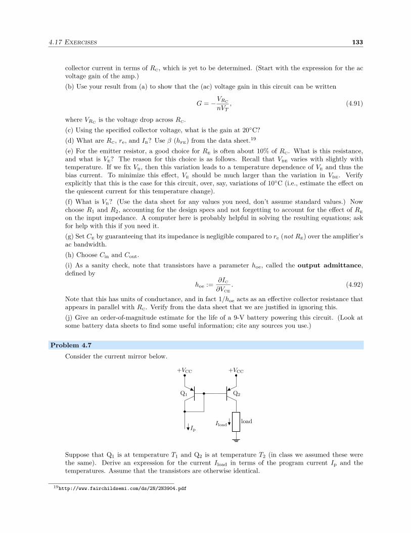
4.17 Exercises 133
collector current in terms of RC, which is yet to be determined. (Start with the expression for the acvoltage gain of the amp.)
(b) Use your result from (a) to show that the (ac) voltage gain in this circuit can be written
G = −VRC
nVT, (4.91)
where VRCis the voltage drop across RC.
(c) Using the specified collector voltage, what is the gain at 20C?
(d) What are RC, re, and IB? Use β (hFE) from the data sheet.19
(e) For the emitter resistor, a good choice for RE is often about 10% of RC. What is this resistance,and what is VE? The reason for this choice is as follows. Recall that VBE varies with slightly withtemperature. If we fix VB, then this variation leads to a temperature dependence of VE and thus thebias current. To minimize this effect, VE should be much larger than the variation in VBE. Verifyexplicitly that this is the case for this circuit, over, say, variations of 10C (i.e., estimate the effect onthe quiescent current for this temperature change).
(f) What is VB? (Use the data sheet for any values you need, don’t assume standard values.) Nowchoose R1 and R2, accounting for the design specs and not forgetting to account for the effect of RE
on the input impedance. A computer here is probably helpful in solving the resulting equations; askfor help with this if you need it.
(g) Set CE by guaranteeing that its impedance is negligible compared to re (not RE) over the amplifier’sac bandwidth.
(h) Choose Cin and Cout.
(i) As a sanity check, note that transistors have a parameter hoe, called the output admittance,defined by
hoe :=∂IC
∂VCE
. (4.92)
Note that this has units of conductance, and in fact 1/hoe acts as an effective collector resistance thatappears in parallel with RC. Verify from the data sheet that we are justified in ignoring this.
(j) Give an order-of-magnitude estimate for the life of a 9-V battery powering this circuit. (Look atsome battery data sheets to find some useful information; cite any sources you use.)
Problem 4.7
Consider the current mirror below.
Q1 Q2
+VCC +VCC
loadIp
Iload
Suppose that Q1 is at temperature T1 and Q2 is at temperature T2 (in class we assumed these werethe same). Derive an expression for the current Iload in terms of the program current Ip and thetemperatures. Assume that the transistors are otherwise identical.
19http://www.fairchildsemi.com/ds/2N/2N3904.pdf

134 Chapter 4. Bipolar Junction Transistors
Problem 4.8
The circuit below is a variation on the transistor current mirror. Compute Iload, assuming that thethree transistors are identical.
IC
Iload = ?Ip
+VCC +VCC
Q2 Q3Q1
Problem 4.9
Consider the circuit below.
β = 100
0.1 µF
Vin
100 kΩ
10 kΩ
Vout
1 kΩ
10 kΩ
+15 V
(a) What is the input impedance at high frequencies?
(b) What is the dc bias level of Vout?
(c) How does the intrinsic emitter resistance enter into the analysis of this circuit? For the specificcomponent values here, how much does it affect the quantities you calculated in (a) and (b)?
Problem 4.10
Consider the common-emitter amplifier shown below, assumed to be biased as needed for the circuitto work normally as an amplifier. Recall that the Miller effect refers to an intrinsic capacitancethat appears across the reverse-biased base–collector junction, shown as capacitance C in the left-handdiagram.

4.17 Exercises 135
vin
RE
RC
+VCC
vout
C
vin
RE
RC
+VCC
vout
Ceff
The reason that the Miller capacitance is a serious problem in a high-gain circuit is that seen as aneffective input capacitance Ceff as shown in the right-hand diagram, the effective capacitance is
Ceff =(
1 + |G|)
C, (4.93)
where G ≈ −RC/RE is the ac voltage gain of the amplifier.
Show that this statement is true by considering the change q in the charge Q on the capacitor due toa change vin in the input voltage.
Problem 4.11
Consider the grounded-emitter amplifier (i.e., a common-emitter amplifier with RE = 0) shownbelow.
2N4401Vin
RC = 10 kΩ
+10 V
Vout
(a) What is the minimum value of Vin that saturates the transistor? Assume a transistor temperatureof 20C, with parameters ICS = 1.75 pA and n = 1.1.20
(b) Suppose you set the dc bias of Vin to 0.54 V. What is the (ac) voltage gain of the amplifier? (Recallthat in this configuration, the gain is limited by the intrinsic emitter resistance.)
(c) Note that, in practice, this circuit has some drawbacks. The emitter resistance varies with IC, andthus with Vin. That means that both the gain and the input impedance of the transistor depend onVin, leading to distortion in the output signal. To see this distortion explicitly, make a plot of the(dc) output voltage Vout as a function of the (dc) input Vin, assuming Vin to be a 36-mV triangle wave
20The parameters in this problem are from the 2N4401 model in LTspice (http://www.linear.com/solutions/ltspice).
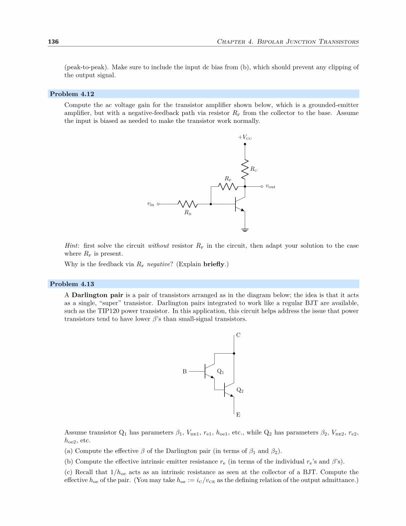
136 Chapter 4. Bipolar Junction Transistors
(peak-to-peak). Make sure to include the input dc bias from (b), which should prevent any clipping ofthe output signal.
Problem 4.12
Compute the ac voltage gain for the transistor amplifier shown below, which is a grounded-emitteramplifier, but with a negative-feedback path via resistor RF from the collector to the base. Assumethe input is biased as needed to make the transistor work normally.
RB
vin
RC
+VCC
vout
RF
Hint: first solve the circuit without resistor RF in the circuit, then adapt your solution to the casewhere RF is present.
Why is the feedback via RF negative? (Explain briefly.)
Problem 4.13
A Darlington pair is a pair of transistors arranged as in the diagram below; the idea is that it actsas a single, “super” transistor. Darlington pairs integrated to work like a regular BJT are available,such as the TIP120 power transistor. In this application, this circuit helps address the issue that powertransistors tend to have lower β’s than small-signal transistors.
Q1
Q2
C
E
B
Assume transistor Q1 has parameters β1, VBE1, re1, hoe1, etc., while Q2 has parameters β2, VBE2, re2,hoe2, etc.
(a) Compute the effective β of the Darlington pair (in terms of β1 and β2).
(b) Compute the effective intrinsic emitter resistance re (in terms of the individual re’s and β’s).
(c) Recall that 1/hoe acts as an intrinsic resistance as seen at the collector of a BJT. Compute theeffective hoe of the pair. (You may take hoe := iC/vCE as the defining relation of the output admittance.)

4.17 Exercises 137
(d) Derive an effective Ebers–Moll equation for the pair, noting that some of the effective “constants”may not be completely constant. Assume the same temperature, ideality, and forward saturationcurrent for both transistors.
Problem 4.14
Consider the folded cascode amplifier shown below. Here, Vbias is an externally imposed, constantbias voltage.
Q1 Q2
RC
+VCC
RE R′C
vout
vin Vbias
(a) Derive an expression for the ac voltage gain.
(b) Explain why this circuit does not suffer from the Miller effect (Problem 4.10). Be brief.
(c) Explain why this circuit is not subject to the Early effect (Section 4.11.5.2). Be brief.

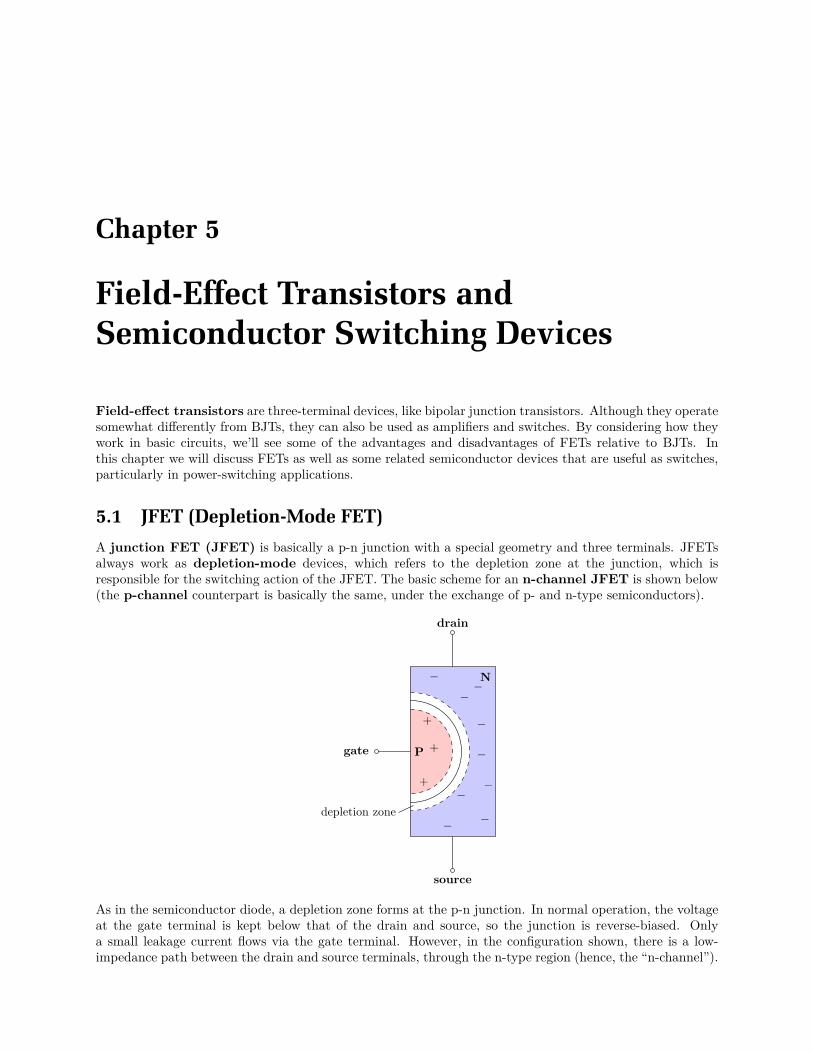
Chapter 5
Field-Effect Transistors andSemiconductor Switching Devices
Field-effect transistors are three-terminal devices, like bipolar junction transistors. Although they operatesomewhat differently from BJTs, they can also be used as amplifiers and switches. By considering how theywork in basic circuits, we’ll see some of the advantages and disadvantages of FETs relative to BJTs. Inthis chapter we will discuss FETs as well as some related semiconductor devices that are useful as switches,particularly in power-switching applications.
5.1 JFET (Depletion-Mode FET)
A junction FET (JFET) is basically a p-n junction with a special geometry and three terminals. JFETsalways work as depletion-mode devices, which refers to the depletion zone at the junction, which isresponsible for the switching action of the JFET. The basic scheme for an n-channel JFET is shown below(the p-channel counterpart is basically the same, under the exchange of p- and n-type semiconductors).
N
P
drain
source
gate
+
−
−−
−
+ −
−
+
−−
−
depletion zone
As in the semiconductor diode, a depletion zone forms at the p-n junction. In normal operation, the voltageat the gate terminal is kept below that of the drain and source, so the junction is reverse-biased. Onlya small leakage current flows via the gate terminal. However, in the configuration shown, there is a low-impedance path between the drain and source terminals, through the n-type region (hence, the “n-channel”).
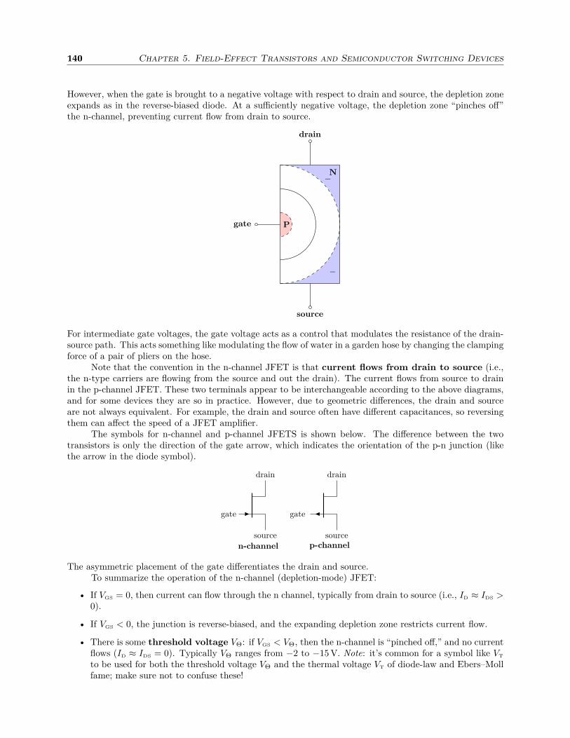
140 Chapter 5. Field-Effect Transistors and Semiconductor Switching Devices
However, when the gate is brought to a negative voltage with respect to drain and source, the depletion zoneexpands as in the reverse-biased diode. At a sufficiently negative voltage, the depletion zone “pinches off”the n-channel, preventing current flow from drain to source.
N
P
drain
source
gate
−
−
For intermediate gate voltages, the gate voltage acts as a control that modulates the resistance of the drain-source path. This acts something like modulating the flow of water in a garden hose by changing the clampingforce of a pair of pliers on the hose.
Note that the convention in the n-channel JFET is that current flows from drain to source (i.e.,the n-type carriers are flowing from the source and out the drain). The current flows from source to drainin the p-channel JFET. These two terminals appear to be interchangeable according to the above diagrams,and for some devices they are so in practice. However, due to geometric differences, the drain and sourceare not always equivalent. For example, the drain and source often have different capacitances, so reversingthem can affect the speed of a JFET amplifier.
The symbols for n-channel and p-channel JFETS is shown below. The difference between the twotransistors is only the direction of the gate arrow, which indicates the orientation of the p-n junction (likethe arrow in the diode symbol).
gate
drain
source
n-channel
gate
drain
sourcep-channel
The asymmetric placement of the gate differentiates the drain and source.To summarize the operation of the n-channel (depletion-mode) JFET:
• If VGS = 0, then current can flow through the n channel, typically from drain to source (i.e., ID ≈ IDS >0).
• If VGS < 0, the junction is reverse-biased, and the expanding depletion zone restricts current flow.
• There is some threshold voltage VΘ: if VGS < VΘ, then the n-channel is “pinched off,” and no currentflows (ID ≈ IDS = 0). Typically VΘ ranges from −2 to −15 V. Note: it’s common for a symbol like VT
to be used for both the threshold voltage VΘ and the thermal voltage VT of diode-law and Ebers–Mollfame; make sure not to confuse these!

5.2 MOSFET (Enhancement-Mode FET) 141
• The forward-biased case VGS > 0 doesn’t normally happen. You may as well just use a diode.
• The JFET is thus a transconductance device, where a voltage controls a current (like the BJT,from the standpoint of the Ebers–Moll equation).
5.2 MOSFET (Enhancement-Mode FET)
A second major class of FETs is the metal-oxide-semiconductor FET (MOSFET), also called theinsulated-gate FET (IGFET). The names refer to the gate terminal, which is connected to a metalconducting layer, and insulated by an oxide layer from the semiconductor regions of the MOSFET. SomeMOSFETs behave as depletion-mode devices, but these are relatively rare. Here we will focus on the muchmore common case of enhancement-mode MOSFETs. The basic scheme for an n-channel MOSFETis shown below (note that the body is a p-type semiconductor, unlike the n-channel JFET; the operatingprinciple is quite different).
PN
N
drain
source
gate
body
−−−−−
−−
−
−
oxide insulator
metal layer
induced n-channel
The drain and source terminals connect to n-type regions, which are embedded in the p-type substrate orbody. In principle MOSFETs have a separate body connection, but these are not always explicitly available(often the body and source terminals are combined into one terminal). The idea here is that if no voltageis applied to the gate, no drain–source current can flow because it will be blocked by one reverse-biasedp-n junction. However, when a positive control voltage (with respect to drain and source) the gate’s E-fieldpulls n-type carriers out of the p-type substrate (the p-type carriers are the majority carrier in the p-typesemiconductor, but n-type carriers are also present as the minority carrier). The n-type carriers bunchedagainst the gate insulator form an effective n-channel, or induced n-channel, that bridges the drain andsource. The diagram shows the induced n-channel as being somewhat asymmetric, as appropriate if VDS > 0.
The symbols for n-channel and p-channel enhancement-mode MOSFETS are shown below. Again,there are extra body connections, but often these are internally shorted to the source.
gatebody
drain
source
n-channel
gatebody
drain
sourcep-channel
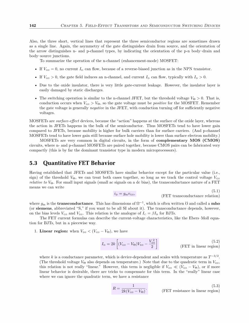
142 Chapter 5. Field-Effect Transistors and Semiconductor Switching Devices
Also, the three short, vertical lines that represent the three semiconductor regions are sometimes drawnas a single line. Again, the asymmetry of the gate distinguishes drain from source, and the orientation ofthe arrow distinguishes n- and p-channel types, by indicating the orientation of the p-n body–drain andbody–source junctions.
To summarize the operation of the n-channel (enhancement-mode) MOSFET:
• If VGS = 0, no current ID can flow, because of a reverse-biased junction as in the NPN transistor.
• If VGS > 0, the gate field induces an n-channel, and current ID can flow, typically with ID > 0.
• Due to the oxide insulator, there is very little gate-current leakage. However, the insulator layer iseasily damaged by static discharges.
• The switching operation is similar to the n-channel JFET, but the threshold voltage VΘ > 0. That is,conduction occurs when VGS > VΘ, so the gate voltage must be positive for the MOSFET. Rememberthe gate voltage is generally negative in the JFET, with conduction turning off for sufficiently negativevoltages.
MOSFETs are surface-effect devices, because the “action” happens at the surface of the oxide layer, whereasthe action in JFETs happens in the bulk of the semiconductor. Thus MOSFETs tend to have lower gaincompared to JFETs, because mobility is higher for bulk carriers than for surface carriers. (And p-channelMOSFETs tend to have lower gain still because surface hole mobility is lower than surface electron mobility.)
MOSFETs are very common in digital circuits, in the form of complementary MOS (CMOS)circuits, where n- and p-channel MOSFETs are paired together, because CMOS pairs can be fabricated verycompactly (this is by far the dominant transistor type in modern microprocessors).
5.3 Quantitative FET Behavior
Having established that JFETs and MOSFETs have similar behavior except for the particular value (i.e.,sign) of the threshold VΘ, we can treat both cases together, so long as we track the control voltage VGS
relative to VΘ. For small input signals (small ac signals on a dc bias), the transconductance nature of a FETmeans we can write
iD = gmvGS,(5.1)
(FET transconductance relation)
where gm is the transconductance. This has dimensions of Ω−1, which is often written and called a mho(or siemens, abbreviated “S,” if you want to be all SI about it). The transconductance depends, however,on the bias levels VGS and VDS. This relation is the analogue of IC = βIB for BJTs.
The FET current formulas can describe the current-voltage characteristics, like the Ebers–Moll equa-tion for BJTs, but in a piecewise way.
1. Linear region: when VDS < (VGS − VΘ), we have
ID = 2k
[
(VGS − VΘ)VDS −V 2
DS
2
]
(5.2)(FET in linear region)
where k is a conductance parameter, which is device-dependent and scales with temperature as T −3/2.(The threshold voltage VΘ also depends on temperature.) Note that due to the quadratic term in VDS,this relation is not really “linear.” However, this term is negligible if VDS ≪ (VGS − VΘ), or if morelinear behavior is desirable, there are tricks to compensate for this term. In the “really” linear casewhere we can ignore the quadratic term, we have a resistance
R =1
2k(VGS − VΘ).
(5.3)(FET resistance in linear region)

5.3 Quantitative FET Behavior 143
This says that the FET in this regime is useful as a voltage-controlled resistor, for example to controlvariable gain or attenuation in a circuit.
Also in the linear region, the transconductance is
gm = 2kVDS,(5.4)
(FET transconductance in linear region)
using Eq. (5.1) in the form gm = ∂ID/∂VGS.
2. Saturation or quadratic region: when VDS > (VGS − VΘ). In this region, ID is independent of VDS,in some sense like the saturated BJT where the transistor no longer directly modulates the collectorcurrent. In this region,
ID = k(VGS − VΘ)2,(5.5)
(FET in saturation region)
and differentiating again to find gm,
gm = 2k(VGS − VΘ) = 2√
kID.
(FET transconductance in saturation region) (5.6)As useful observation in this region is thus to use gm ∝
√ID, so that gm can be found at different ID
even when it is only known at one point.
3. Subthreshold region: when ID is small, because the gate voltage is close to or below the VΘ. Thesimplest model for this region is that the current decreases linearly until VGS goes below VΘ, and atthat point the current ceases. A more careful model in this region gives diode-law-like behavior
ID = I0 e(VGS−VΘ)/nVT ,(5.7)
(FET in subthreshold region)
where VT is the thermal voltage from the diode law and Ebers–Moll equations. Note that in a JFET,drain current via the gate can become significant. Then gm is given by
gm =I0
nVT
e(VGS−VΘ)/nVT =ID
nVT
,
(FET transconductance in subthreshold region) (5.8)according to the exponential law.
5.3.1 Visualization
It’s much easier to understand the modeling relations as given above by visualizing them. As with thecharacteristic curves for BJTs (Section 4.14), there are standard characteristic curves for FETs. One exampleshown below is for the BF256B, a radio-frequency, small-signal, n-channel (depletion-mode) JFET. Againthe control signal VGS labels the different curves, and the results give the drain current ID as it varies withapplied drain–source voltage VDS.
144 Chapter 5. Field-Effect Transistors and Semiconductor Switching Devices
linear regionsaturation region
VDS (V)0 102 4 6 8
ID (
mA
)
10
0
5
IDSS
VGSo=o0
VGSo=o-0.4oV
VGSo=o-0.8oV
VGSo=o-1.2oV
VGSo=o-1.6oVVGSo=o-2.0oV
BF256B
For this transistor model1 the threshold is VΘ = −2.3 V (but ranges from −0.5 V to −8 V in the data sheet!);also IDSS ranges from 6 to 13 mA in the data sheet.2 Recall that the boundary between the linear andsaturation regions is given by the condition VGS−VΘ = VDS, although these labels are unfortunately reversedfrom what you might expect after looking at an analogous diagram of BJT characteristic curves (where recallthat saturation occurs to the left and linearity occurs to the right). In the FET case, the “linearity” of thelinear region refers to the linear behavior for small VDS (and small ID, where the device acts as a variableresistor across the drain–source connections (controlled by VGS). In the saturation region, the drain currentis insensitive to the applied VDS, but is modulated quadratically with VGS (hence this is also the quadraticregion). Note that Eq. (5.5) predicts no dependence on VDS, but the SPICE-model equations used in theplot allow some linear variation in this region [otherwise, the equations are basically (5.2) and (5.5)]. Thesubthreshold region is not shown (and not commonly included in SPICE models), but would occur along thebottom edge of the plot. Also, for large enough VDS, the JFET will of course eventually break down (pastthe right-hand edge of the plot), causing the characteristic curves to turn sharply upward; this effect is alsonot illustrated here.
As a somewhat different example, the characteristic curves for the J111 n-channel JFET (designed forswitching larger currents) is shown below. In this model,3 VΘ = −5.36 V, and IDSS is much larger, almost100 mA. The behavior is generally similar to that of the 2N3819, but on a larger scale of ID and VGS. Notealso the larger slopes in the saturation region, particularly as VGS approaches zero.
1The parameters are from the SPICE model from the MicroSim libarary, http://ppd.fnal.gov/experiments/cdms/old_
files/electronics/FLIP/3U/QampDiscrete/proto/schematics_layouts/JFET.LIB.2https://www.fairchildsemi.com/datasheets/BF/BF256B.pdf3The parameters here are from the Philips SPICE model; see http://web.rfoe.net:8000/ziliaoxiazai/PHILIPS/models/
spicespar/data/j111.html.

5.3 Quantitative FET Behavior 145
VDS (V)0 102 4 6 8
ID (
mA
)
120
0
20
40
60
80
100IDSS
VGSo=o0
VGSo=o-1oV
VGSo=o-2oV
VGSo=o-3oV
VGSo=o-4oVVGSo=o-5oV
J111
To show just one more example, the characteristic curves of a popular small-signal (n-channel, enhancement-mode) MOSFET are shown in the plot below.
thermal overload
VDS (V)0 51 2 3 4
ID (
mA
)
400
0
100
200
300
VGSo=o1.5oV
VGSo=o2oV
VGSo=o2.5oV
VGSo=o3oV
VGSo=o3.5oV
VGSo=o4oV2N7000
The basic feature of enhancement mode is apparent, because now all the curves correspond to positive VGS
(the model used to make this plot assumed VΘ = 1 V. The modeling for a MOSFET is considerably morecomplex than that of a JFET,4 although the basic shape of the curves is the same. Note the much larger“gain” (i.e., transconductance, or amount of current modulated by a gate-voltage change) compared to theJFET in the plots above; recall that this is not very characteristic of an enhancement-mode device (whichrelies on lower surface mobility vs. larger bulk mobility). In fact, this small-signal transistor is only ratedfor 350 mW, so much of the plot corresponds to a potentially fried MOSFET (shaded “thermal overload”region). One final curious feature is that in the saturation regime, the curves look quite level, but actuallydecrease slightly with increasing VDS—this indicates a large, but negative effective saturation impedance asseen at the drain (in the grounded-source amplifier).
4See, for example, the HSPICE MOSFET Models Manual (http://www.ece.tamu.edu/~spalermo/ecen474/hspice_mosfet.
pdf), which goes into many possibilities. The plot here assumes a “LEVEL 3” model, with parameters published by SupertexInc.

146 Chapter 5. Field-Effect Transistors and Semiconductor Switching Devices
5.4 Basic FET Circuits
Now let’s see how to apply FETs in some basic circuits. Many of the JFET circuits here have analogues toBJT circuits, and analyzing these will both introduce analysis techniques for FET circuits and highlight thedifferences as compared to BJTs.
5.4.1 JFET Current Source
A simple JFET circuit is the JFET current source, show below.
Iload = IDSS
load
+VDD
The idea is to operate the JFET in the saturation region, where ID is independent of VDS, allowing the JFETto adjust the load voltage to regulate its current. Since the gate and source are shorted (and grounded),VGS = 0. Then using Eq. (5.5), we find the constant current
ID = kV 2Θ =: IDSS,
(5.9)(JFET regulated current)
where IDSS is the drain current at zero gate–source voltage (i.e., effectively the maximum JFET current).Looking at the characteristic curves above for the 2N3819, you can indeed see that ID is relatively
insensitive to VDS above about 2 V in this application, so it makes a fairly good current source (the effectiveresistance with the slope in the plot as shown is 38 kΩ). From looking at the characteristic curves of the J111JFET above, it is apparent that it is not especially good as a current source (with an effective resistance ofabout 7 kΩ). From looking at these same plots, it is apparent that it is also possible to vary the regulatedcurrent by reducing VGS (say, by inserting a resistor, especially a variable resistor, between the JFET sourceand ground).
The advantage of this circuit, compared to the BJT current source, is its simplicity. The disadvantage ismore serious: IDSS varies significantly between devices. However, it is possible to get hand-picked FETs withparticular values of IDSS, called current-regulator diodes (something like Zener diodes, but for currentinstead of voltage). A good example is the 1N5283–1N5314 series, which covers a nominal current range of0.22–4.70 mA.5
5.4.2 JFET Source Follower
The next circuit is the JFET analogue of the BJT emitter follower.
5https://www.centralsemi.com/get_document.php?cmp=1&mergetype=pd&mergepath=pd&pdf_id=1N5283-5314.PDF
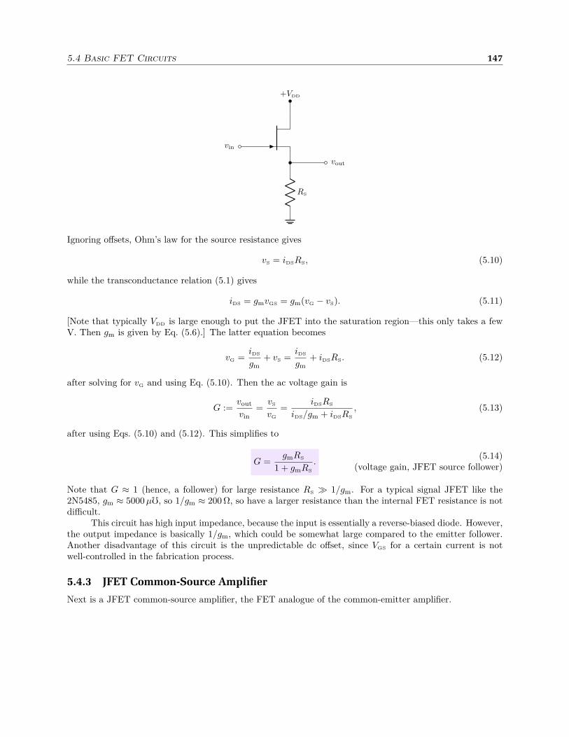
5.4 Basic FET Circuits 147
RS
vout
vin
+VDD
Ignoring offsets, Ohm’s law for the source resistance gives
vS = iDSRS, (5.10)
while the transconductance relation (5.1) gives
iDS = gmvGS = gm(vG − vS). (5.11)
[Note that typically VDD is large enough to put the JFET into the saturation region—this only takes a fewV. Then gm is given by Eq. (5.6).] The latter equation becomes
vG =iDS
gm+ vS =
iDS
gm+ iDSRS. (5.12)
after solving for vG and using Eq. (5.10). Then the ac voltage gain is
G :=vout
vin=
vS
vG
=iDSRS
iDS/gm + iDSRS
, (5.13)
after using Eqs. (5.10) and (5.12). This simplifies to
G =gmRS
1 + gmRS
.(5.14)
(voltage gain, JFET source follower)
Note that G ≈ 1 (hence, a follower) for large resistance RS ≫ 1/gm. For a typical signal JFET like the2N5485, gm ≈ 5000 µ, so 1/gm ≈ 200 Ω, so have a larger resistance than the internal FET resistance is notdifficult.
This circuit has high input impedance, because the input is essentially a reverse-biased diode. However,the output impedance is basically 1/gm, which could be somewhat large compared to the emitter follower.Another disadvantage of this circuit is the unpredictable dc offset, since VGS for a certain current is notwell-controlled in the fabrication process.
5.4.3 JFET Common-Source Amplifier
Next is a JFET common-source amplifier, the FET analogue of the common-emitter amplifier.

148 Chapter 5. Field-Effect Transistors and Semiconductor Switching Devices
C
vin
RG
RD
+VDD
vout
Here, RG maintains the dc bias of VGS at ground, but allows ac modulation of the gate via the capacitor C.If VGS = 0, the quiescent current is ID = IDSS, as in the JFET current source (thus assuming that VDD
is large enough to put the JFET into saturation). Then the output is biased at
Vout = VDD − IDRD. (5.15)
This bias level may be adjusted by introducing a source resistor, thus lowering VGS and decreasing IDS, thoughbiasing this amplifier is more difficult than its BJT counterpart, due to large variation among particulardevices in the JFET’s ID at a given VGS.
For small ac signals,vout = vD = −iDRD. (5.16)
Then using the transconductance relation (5.1),
iD = gmvGS = gmvin, (5.17)
we havevout = −gmRDvin, (5.18)
which implies a voltage gain
G = −gmRD.(5.19)
(voltage gain, grounded-source amplifier)
So for example, if RD = 1 kΩ and for the 2N5485, 1/gm = 200 Ω, then G = −5, which is not a huge gain.By contrast, in the common-emitter amplifier, using the intrinsic emitter resistance re = 25 Ω at IC = 1 mA,the gain is about 8× larger (because re is eight times smaller than 1/gm). So the advantage of the JFET ishigh input impedance (good for input stages of amplifiers, especially op-amps), the advantage of the BJT isbetter speed (due to lower capacitance) and amplification.
The idea is basically the same if we also add a source resistor (which could be useful for setting the dcbias, as we noted above), as shown below.

5.4 Basic FET Circuits 149
RS
C
vin
RG
RD
+VDD
vout
The analysis is a combination of the analysis of the grounded-source amplifier above and that of the sourcefollower in the previous section. The result is
G = − gmRD
1 + gmRS
= − RD
RS + g−1m
.
(voltage gain, common-source amplifier) (5.20)The last expression here makes the parallel to the BJT more clear—this amplifier is closely analogous to theBJT common-emitter amplifier [see Eq. (4.82)], where 1/gm plays the role of the intrinsic emitter resistancere. Like the common-emitter case, RS acts as a “source-degeneration” resistor [see Section 4.12], reducingthe gain, and it dominates the effect of gm if it is large enough, so that the gain simplifies to G = −RD/RS.
5.4.4 JFET Differential Amplifier
A straightforward generalization of the BJT differential amplifier of Section 4.10 is its JFET counterpart.The advantage is high input impedance, while the main disadvantage is difficulty in designing and tuningthe circuit due to the intrinsic uncertainty in the JFET device parameters.
v+ v−RS RS
RSS
−VSS
RD
+VDD
RD
+VDD
vout
The analysis here is closely analogous to that of the BJT case, so we will only sketch the idea. Assuming apurely differential (ac) input ∆v := v+ − v−, the voltage drop across RSS is fixed, so the two transistors act
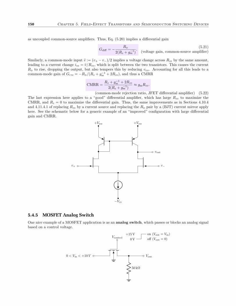
150 Chapter 5. Field-Effect Transistors and Semiconductor Switching Devices
as uncoupled common-source amplifiers. Thus, Eq. (5.20) implies a differential gain
Gdiff = − RD
2(RS + g−1m )
.(5.21)
(voltage gain, common-source amplifier)
Similarly, a common-mode input v := (v+− v−)/2 implies a voltage change across RSS by the same amount,leading to a current change iSS = v/RSS, which is split between the two transistors. This causes the currentRD to rise, dropping the output, but also tempers this by reducing vGS. Accounting for all this leads to acommon-mode gain of GCM = −RD/(RS + g−1
m + 2RSS), and thus a CMRR
CMRR =RS + g−1
m + 2RSS
2(RS + g−1m )
≈ gmRSS.
(common-mode rejection ratio, JFET differential amplifier) (5.22)The last expression here applies to a “good” differential amplifier, which has large RSS to maximize theCMRR, and RS = 0 to maximize the differential gain. Thus, the same improvements as in Sections 4.10.4and 4.11.4.1 of replacing RSS by a current source and replacing the RD pair by a (BJT) current mirror applyhere. See the schematic below for a generic example of an “improved” configuration with large differentialgain and CMRR.
v+ v−
vout
−VSS
+VDD +VDD
5.4.5 MOSFET Analog Switch
One nice example of a MOSFET application is as an analog switch, which passes or blocks an analog signalbased on a control voltage.
Vcontrol
0 < Vin < +10 V Vout
50 kΩ
off (Vout = 0)
on (Vout = Vin)
0 V
+15 V
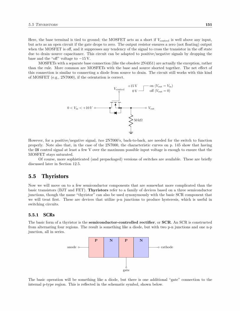
5.5 Thyristors 151
Here, the base terminal is tied to ground; the MOSFET acts as a short if Vcontrol is well above any input,but acts as an open circuit if the gate drops to zero. The output resistor ensures a zero (not floating) outputwhen the MOSFET is off, and it suppresses any tendency of the signal to cross the transistor in the off statedue to drain–source capacitance. This circuit can be adapted to positive/negative signals by dropping thebase and the “off” voltage to −15 V.
MOSFETs with a separate base connection (like the obsolete 2N4351) are actually the exception, ratherthan the rule. More common are MOSFETs with the base and source shorted together. The net effect ofthis connection is similar to connecting a diode from source to drain. The circuit still works with this kindof MOSFET (e.g., 2N7000), if the orientation is correct.
Vcontrol
0 < Vin < +10 V Vout
50 kΩ
off (Vout = 0)
on (Vout = Vin)
0 V
+15 V
However, for a positive/negative signal, two 2N7000’s, back-to-back, are needed for the switch to functionproperly. Note also that, in the case of the 2N7000, the characteristic curves on p. 145 show that havingthe ON control signal at least a few V over the maximum possible input voltage is enough to ensure that theMOSFET stays saturated.
Of course, more sophisticated (and prepackaged) versions of switches are available. These are brieflydiscussed later in Section 12.5.
5.5 Thyristors
Now we will move on to a few semiconductor components that are somewhat more complicated than thebasic transistors (BJT and FET). Thyristors refer to a family of devices based on a three semiconductorjunctions, though the name “thyristor” can also be used synonymously with the basic SCR component thatwe will treat first. These are devices that utilize p-n junctions to produce hysteresis, which is useful inswitching circuits.
5.5.1 SCRs
The basic form of a thyristor is the semiconductor-controlled rectifier, or SCR. An SCR is constructedfrom alternating four regions. The result is something like a diode, but with two p-n junctions and one n-pjunction, all in series.
P N P N
anode cathode
gate
The basic operation will be something like a diode, but there is one additional “gate” connection to theinternal p-type region. This is reflected in the schematic symbol, shown below.

152 Chapter 5. Field-Effect Transistors and Semiconductor Switching Devices
gate
anode cathode
Thinking of the p-n junctions as diode-type junctions is only useful in understanding the “OFF” state; ineither direction there is a reverse-biased diode, so no current can flow. However, to understand the switchingbehavior of the SCR, it helps to think of the p-n-p stack to the left as a PNP transistor, and the n-p-n stackto the right as an NPN transistor. Since the inner two regions are common to each transistor, the transistorsare interconnected as shown in the equivalent circuit below.
gate
anode
cathode
Again, if no current is initially flowing in the circuit, then both transistors are OFF, and no current canflow from anode to cathode, because the current would have to pass via the collector of one or the othertransistor.
However, if a (sufficiently large) anode–cathode current is already flowing in the circuit, then thecollector current of the NPN transistor ensures the PNP transistor is ON (since the current comes via theemitter–base junction), and the collector current of the PNP transistor flows through the base–emitterjunction of the NPN transistor, ensuring that it is ON.
As an aside, note that although this transistor model is a useful way to understand how an SCR works,an SCR can’t necessarily be replaced by two transistors. For example, the collector leakage current of oneof the transistors could supply sufficient base current to turn the other ON, in which case this SCR OFF statewouldn’t work as described above.
So now we see that there are two possible states, where current is flowing or not, and the states areself-sustaining (the current-flowing state of course requiring a sufficient forward voltage). Then the questionis, how can we transition between the states? In particular, if no current is flowing, how can we get thecurrent started? There are two useful answers to this in practice:
1. Inject some gate current (flowing from gate to cathode). This turns on the NPN transistor, whichturns on the PNP transistor, and the SCR transitions to the conducting state.
2. Bring the forward voltage sufficiently high that the reverse-biased junction breaks down. Just beforethe breakdown, the forward voltage can be quite high (hundreds of volts), but after breakdown, theforward voltage will become much smaller, on the order of a volt. Note that a gate current will reducethe breakdown voltage, and a gate current above a switching threshold brings the breakdown voltageto essentially zero.
To make a transition in the other direction, or that is, to stop the conduction, the only way is to bring theforward current to zero (or equivalently, drop the forward voltage to zero). This “resets” the SCR into thenon-conducting state, assuming there is no gate current is off.
As an example, the small-signal S401E SCR has 1-A maximum (rms) current, 400-V off voltage (ineither direction), a gate trigger current guaranteed to be in the range of 1–10 mA, a 1.6-V maximum forward-conduction voltage, and a maximum gate forward voltage of 1.5 V.
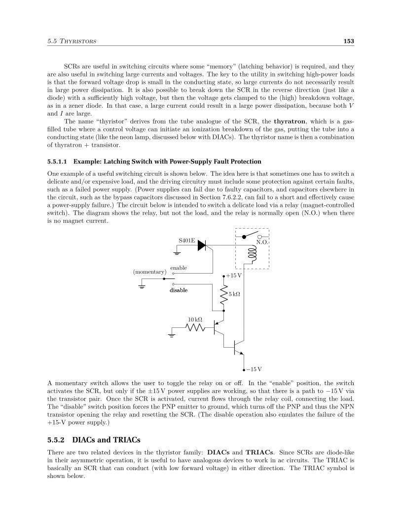
5.5 Thyristors 153
SCRs are useful in switching circuits where some “memory” (latching behavior) is required, and theyare also useful in switching large currents and voltages. The key to the utility in switching high-power loadsis that the forward voltage drop is small in the conducting state, so large currents do not necessarily resultin large power dissipation. It is also possible to break down the SCR in the reverse direction (just like adiode) with a sufficiently high voltage, but then the voltage gets clamped to the (high) breakdown voltage,as in a zener diode. In that case, a large current could result in a large power dissipation, because both Vand I are large.
The name “thyristor” derives from the tube analogue of the SCR, the thyratron, which is a gas-filled tube where a control voltage can initiate an ionization breakdown of the gas, putting the tube into aconducting state (like the neon lamp, discussed below with DIACs). The thyristor name is then a combinationof thyratron + transistor.
5.5.1.1 Example: Latching Switch with Power-Supply Fault Protection
One example of a useful switching circuit is shown below. The idea here is that sometimes one has to switch adelicate and/or expensive load, and the driving circuitry must include some protection against certain faults,such as a failed power supply. (Power supplies can fail due to faulty capacitors, and capacitors elsewhere inthe circuit, such as the bypass capacitors discussed in Section 7.6.2.2, can fail to a short and effectively causea power-supply failure.) The circuit below is intended to switch a delicate load via a relay (magnet-controlledswitch). The diagram shows the relay, but not the load, and the relay is normally open (N.O.) when thereis no magnet current.
enable
disabledisable
(momentary)
S401E N.O.
5 kΩ
+15 V
10 kΩ
−15 V
A momentary switch allows the user to toggle the relay on or off. In the “enable” position, the switchactivates the SCR, but only if the ±15 V power supplies are working, so that there is a path to −15 V viathe transistor pair. Once the SCR is activated, current flows through the relay coil, connecting the load.The “disable” switch position forces the PNP emitter to ground, which turns off the PNP and thus the NPNtransistor opening the relay and resetting the SCR. (The disable operation also emulates the failure of the+15-V power supply.)
5.5.2 DIACs and TRIACs
There are two related devices in the thyristor family: DIACs and TRIACs. Since SCRs are diode-likein their asymmetric operation, it is useful to have analogous devices to work in ac circuits. The TRIAC isbasically an SCR that can conduct (with low forward voltage) in either direction. The TRIAC symbol isshown below.

154 Chapter 5. Field-Effect Transistors and Semiconductor Switching Devices
gate
This component is basically equivalent to two SCRs, oppositely oriented and wired in parallel, with a commongate, as shown below.
gate
The idea is similar with a DIAC, but this component has no gate; the intent is for this device to conduct bybringing the voltage above threshold (in either direction), to break down the device into conduction.
While it’s useful to think of both devices as a combination of two SCRs, they are fabricated in a simpler wayas a single stack of junctions. For example, the DIAC, because it doesn’t need a gate connection, can befabricated as a p-n-p stack. The symmetry of the stack allows for symmetric-breakdown operation. DIACsare typically fabricated with breakdown voltages in the range of 32–40 V. Gas-discharge lamps can also workin a similar way to DIACs. For example, the small NE-2 neon lamp has a breakdown voltage of 90 V (i.e.,it does not conduct until the voltage exceeds 90 V in either direction), and the discharge-state (i.e., lit)voltage drops to around 60 V when the lamp conducts. The nominal conduction current is about 0.5 mA,so if used as a lamp across 120 V ac, a dropping resistor of around 100 kΩ is necessary to limit the lampcurrent. However, for switching applications, a neon lamp can function in place of a DIAC, for example inthe dimmer circuit to follow.
5.5.2.1 Light Dimmer
One of the most important applications of thyristor devices is in dimmers for ac lighting circuits. There area number of designs, but a common DIAC–TRIAC design is shown below.
load C
R2
R1
dim
bright
As each “pulse” (of either sign) from the ac source begins, the TRIAC is initially off, and the voltage beginsto charge the capacitor via R1 + R2. Once the capacitor charges to the breakdown voltage of the DIAC(around 30 V), it conducts, and discharges the capacitor via R2 through the TRIAC gate, causing it toconduct. The TRIAC continues to conduct until the end of the pulse, supplying current to the load duringthe last part of the cycle, and the capacitor also discharges and resets before the next voltage pulse. Thenet result is that the load is only on for part of each cycle; the voltage presented to the load is illustratedbelow.
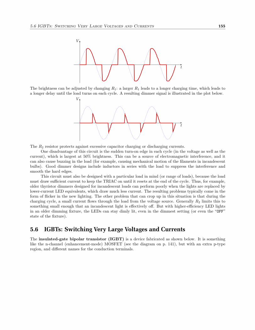
5.6 IGBTs: Switching Very Large Voltages and Currents 155
V
t
The brightness can be adjusted by changing R1: a larger R1 leads to a longer charging time, which leads toa longer delay until the load turns on each cycle. A resulting dimmer signal is illustrated in the plot below.
V
t
The R2 resistor protects against excessive capacitor charging or discharging currents.One disadvantage of this circuit is the sudden turn-on edge in each cycle (in the voltage as well as the
current), which is largest at 50% brightness. This can be a source of electromagnetic interference, and itcan also cause buzzing in the load (for example, causing mechanical motion of the filaments in incandescentbulbs). Good dimmer designs include inductors in series with the load to suppress the interference andsmooth the hard edges.
This circuit must also be designed with a particular load in mind (or range of loads), because the loadmust draw sufficient current to keep the TRIAC on until it resets at the end of the cycle. Thus, for example,older thyristor dimmers designed for incandescent loads can perform poorly when the lights are replaced bylower-current LED equivalents, which draw much less current. The resulting problems typically come in theform of flicker in the new lighting. The other problem that can crop up in this situation is that during thecharging cycle, a small current flows through the load from the voltage source. Generally R2 limits this tosomething small enough that an incandescent light is effectively off. But with higher-efficiency LED lightsin an older dimming fixture, the LEDs can stay dimly lit, even in the dimmest setting (or even the “OFF”state of the fixture).
5.6 IGBTs: Switching Very Large Voltages and Currents
The insulated-gate bipolar transistor (IGBT) is a device fabricated as shown below. It is somethinglike the n-channel (enhancement-mode) MOSFET (see the diagram on p. 141), but with an extra p-typeregion, and different names for the conduction terminals.
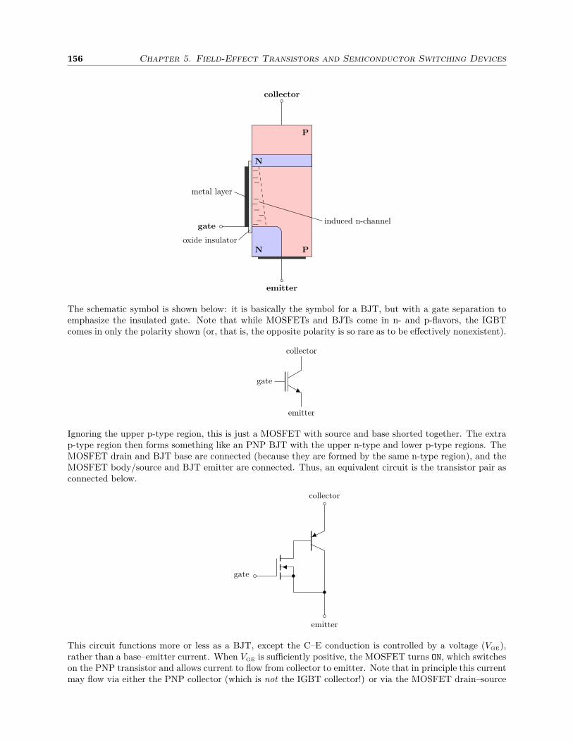
156 Chapter 5. Field-Effect Transistors and Semiconductor Switching Devices
P
N
N P
collector
emitter
gate −−−−−
−−
−
−
oxide insulator
metal layer
induced n-channel
The schematic symbol is shown below: it is basically the symbol for a BJT, but with a gate separation toemphasize the insulated gate. Note that while MOSFETs and BJTs come in n- and p-flavors, the IGBTcomes in only the polarity shown (or, that is, the opposite polarity is so rare as to be effectively nonexistent).
gate
collector
emitter
Ignoring the upper p-type region, this is just a MOSFET with source and base shorted together. The extrap-type region then forms something like an PNP BJT with the upper n-type and lower p-type regions. TheMOSFET drain and BJT base are connected (because they are formed by the same n-type region), and theMOSFET body/source and BJT emitter are connected. Thus, an equivalent circuit is the transistor pair asconnected below.
gate
collector
emitter
This circuit functions more or less as a BJT, except the C–E conduction is controlled by a voltage (VGE),rather than a base–emitter current. When VGE is sufficiently positive, the MOSFET turns ON, which switcheson the PNP transistor and allows current to flow from collector to emitter. Note that in principle this currentmay flow via either the PNP collector (which is not the IGBT collector!) or via the MOSFET drain–source
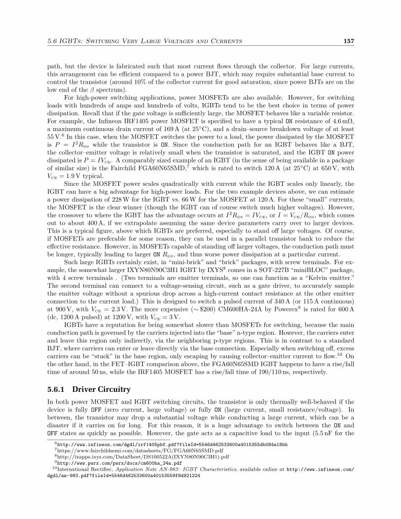
5.6 IGBTs: Switching Very Large Voltages and Currents 157
path, but the device is fabricated such that most current flows through the collector. For large currents,this arrangement can be efficient compared to a power BJT, which may require substantial base current tocontrol the transistor (around 10% of the collector current for good saturation, since power BJTs are on thelow end of the β spectrum).
For high-power switching applications, power MOSFETs are also available. However, for switchingloads with hundreds of amps and hundreds of volts, IGBTs tend to be the best choice in terms of powerdissipation. Recall that if the gate voltage is sufficiently large, the MOSFET behaves like a variable resistor.For example, the Infineon IRF1405 power MOSFET is specified to have a typical ON resistance of 4.6 mΩ,a maximum continuous drain current of 169 A (at 25C), and a drain–source breakdown voltage of at least55 V.6 In this case, when the MOSFET switches the power to a load, the power dissipated by the MOSFETis P = I2RDS while the transistor is ON. Since the conduction path for an IGBT behaves like a BJT,the collector–emitter voltage is relatively small when the transistor is saturated, and the IGBT ON powerdissipated is P = IVCE. A comparably sized example of an IGBT (in the sense of being available in a packageof similar size) is the Fairchild FGA60N65SMD,7 which is rated to switch 120 A (at 25C) at 650 V, withVCE = 1.9 V typical.
Since the MOSFET power scales quadratically with current while the IGBT scales only linearly, theIGBT can have a big advantage for high-power loads. For the two example devices above, we can estimatea power dissipation of 228 W for the IGBT vs. 66 W for the MOSFET at 120 A. For these “small” currents,the MOSFET is the clear winner (though the IGBT can of course switch much higher voltages). However,the crossover to where the IGBT has the advantage occurs at I2RDS = IVCE, or I = VCE/RDS, which comesout to about 400 A, if we extrapolate assuming the same device parameters carry over to larger devices.This is a typical figure, above which IGBTs are preferred, especially to stand off large voltages. Of course,if MOSFETs are preferable for some reason, they can be used in a parallel transistor bank to reduce theeffective resistance. However, in MOSFETs capable of standing off larger voltages, the conduction path mustbe longer, typically leading to larger ON RDS, and thus worse power dissipation at a particular current.
Such large IGBTs certainly exist, in “mini-brick” and “brick” packages, with screw terminals. For ex-ample, the somewhat larger IXYN80N90C3H1 IGBT by IXYS8 comes in a SOT-227B “miniBLOC” package,with 4 screw terminals . (Two terminals are emitter terminals, so one can function as a “Kelvin emitter.”The second terminal can connect to a voltage-sensing circuit, such as a gate driver, to accurately samplethe emitter voltage without a spurious drop across a high-current contact resistance at the other emitterconnection to the current load.) This is designed to switch a pulsed current of 340 A (or 115 A continuous)at 900 V, with VCE = 2.3 V. The more expensive (∼ $200) CM600HA-24A by Powerex9 is rated for 600 A(dc, 1200 A pulsed) at 1200 V, with VCE = 3 V.
IGBTs have a reputation for being somewhat slower than MOSFETs for switching, because the mainconduction path is governed by the carriers injected into the “base” n-type region. However, the carriers enterand leave this region only indirectly, via the neighboring p-type regions. This is in contrast to a standardBJT, where carriers can enter or leave directly via the base connection. Especially when switching off, excesscarriers can be “stuck” in the base region, only escaping by causing collector–emitter current to flow.10 Onthe other hand, in the FET–IGBT comparison above, the FGA60N65SMD IGBT happens to have a rise/falltime of around 50 ns, while the IRF1405 MOSFET has a rise/fall time of 190/110 ns, respectively.
5.6.1 Driver Circuitry
In both power MOSFET and IGBT switching circuits, the transistor is only thermally well-behaved if thedevice is fully OFF (zero current, large voltage) or fully ON (large current, small resistance/voltage). Inbetween, the transistor may drop a substantial voltage while conducting a large current, which can be adisaster if it carries on for long. For this reason, it is a huge advantage to switch between the ON andOFF states as quickly as possible. However, the gate acts as a capacitive load to the input (5.5 nF for the
6http://www.infineon.com/dgdl/irf1405pbf.pdf?fileId=5546d462533600a4015355db084a18bb7https://www.fairchildsemi.com/datasheets/FG/FGA60N65SMD.pdf8http://ixapps.ixys.com/DataSheet/DS100522A(IXYN80N90C3H1).pdf9http://www.pwrx.com/pwrx/docs/cm600ha_24a.pdf
10International Rectifier, Application Note AN-983: IGBT Characteristics, available online at http://www.infineon.com/
dgdl/an-983.pdf?fileId=5546d462533600a40153559f8d921224

158 Chapter 5. Field-Effect Transistors and Semiconductor Switching Devices
IRF1405, 2.9 nF for the FGA60N65SMD, 4.6 nF for the IXYN80N90C3H1), and to change the gate voltagerapidly requires a large, transient current. Thus, such high-power devices typically require special gate-driver circuitry, typically consisting of a pair of smaller FETs or BJTs acting as a fast push-pull buffer.These parts are conveniently packaged in some integrated gate-driver IC’s; one example with a relativelylarge current capability is the UCC37321/UCC37322 by TI,11 which can drive a 9-A peak current, with theoutput switching between ground and a maximum power supply voltage of +15 V (the UCC37321 inverts theinput signal in the sense of a logic inversion, as in Section 9.3.1, while the UCC37322 performs no inversion).An driver example driving up to 340 A (pulsed) current through a load at high voltage via a power IGBT isshown below.
UCC37322
5 Ω
+15 V
Vin
+5 V
0 V OFF
ON
IN
ENB
Venable
load
+340 V
IXYN80N90C3H1
1.5KE400A
P6KE20CA
1N5819
The driver takes a TTL-compatible input (see Section 11.4), but the ON level can also be up to +15 V. Thedriver also has an ENABLE input, which forces the output LOW, close to 0 V (this is also true on the invertingUCC37321), independent of the input voltage.
A number of other components ensure proper operation and protection of the switching transistor.First, the 5-Ω gate resistor limits the gate current to 15 V/5 Ω = 3 A in the worst case of a short to ground,ignoring the effects of capacitance, etc. The data sheet implies a minimum value of 2 Ω for this resistance,and gives specifications for up to 15 Ω. This resistance limits the current into the gate capacitance, easingdemands on the driver and helping to control against voltage overshoot. The 1N5819 Schottky diodes onthe driver output clamp the output voltage to the power-supply range, preventing output overshoot; theSchottky diodes are fast and have a (relatively) small forward voltage. There is also a transient-voltagesuppressor (TVS) on the IGBT gate, which is basically two back-to-back Zener diodes. The P6KE20CATVS break down if the voltage exceeds 20 V in either direction (and is rated for 600 W), protecting agains gateovervoltages (which can come from capacitive coupling via the IGBT as well as from the driver). Finally,as with many IGBTs, the IXYN80N90C3H1 incorporates an internal reverse C–E diode, so that it onlystands off voltage in one direction—the device is not designed to stand off high reverse voltages, so the diodeoffers protection in the event of (intentional or unintentional) reverse transient voltages. However, it is goodpractice to include another (unidirectional) TVS to protect against reverse and overvoltage transients. The1.5KE400A TVS acts as a fast Zener diode that breaks down at 400 V and can handle 1.5 kW.
5.6.2 Inverter Circuits
One important application of power MOSFET and IGBT switching circuits is the inverter, which is usedto convert dc to ac signals. An example of a half-bridge inverter is shown below, where a push–pull pairof MOSFETs switches one side of a load between ±V , giving a square-wave ac signal of amplitude V .
11http://www.ti.com/lit/ds/symlink/ucc27322.pdf
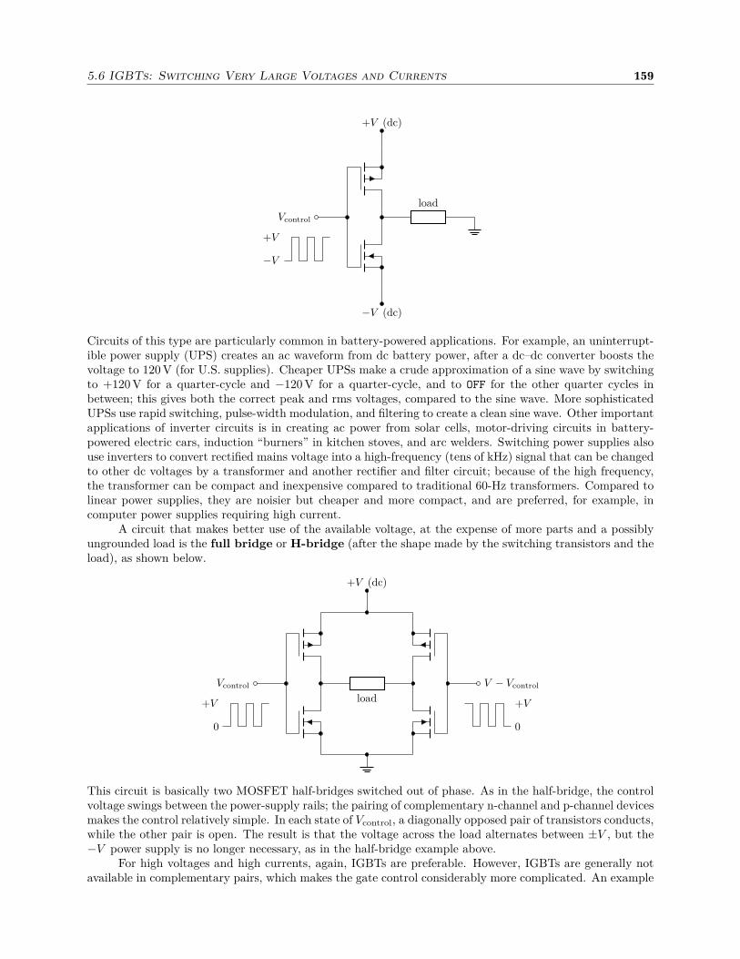
5.6 IGBTs: Switching Very Large Voltages and Currents 159
+V (dc)
−V (dc)
load
Vcontrol
+V
−V
Circuits of this type are particularly common in battery-powered applications. For example, an uninterrupt-ible power supply (UPS) creates an ac waveform from dc battery power, after a dc–dc converter boosts thevoltage to 120 V (for U.S. supplies). Cheaper UPSs make a crude approximation of a sine wave by switchingto +120 V for a quarter-cycle and −120 V for a quarter-cycle, and to OFF for the other quarter cycles inbetween; this gives both the correct peak and rms voltages, compared to the sine wave. More sophisticatedUPSs use rapid switching, pulse-width modulation, and filtering to create a clean sine wave. Other importantapplications of inverter circuits is in creating ac power from solar cells, motor-driving circuits in battery-powered electric cars, induction “burners” in kitchen stoves, and arc welders. Switching power supplies alsouse inverters to convert rectified mains voltage into a high-frequency (tens of kHz) signal that can be changedto other dc voltages by a transformer and another rectifier and filter circuit; because of the high frequency,the transformer can be compact and inexpensive compared to traditional 60-Hz transformers. Compared tolinear power supplies, they are noisier but cheaper and more compact, and are preferred, for example, incomputer power supplies requiring high current.
A circuit that makes better use of the available voltage, at the expense of more parts and a possiblyungrounded load is the full bridge or H-bridge (after the shape made by the switching transistors and theload), as shown below.
+V (dc)
load
Vcontrol
+V
0
V − Vcontrol
0
+V
This circuit is basically two MOSFET half-bridges switched out of phase. As in the half-bridge, the controlvoltage swings between the power-supply rails; the pairing of complementary n-channel and p-channel devicesmakes the control relatively simple. In each state of Vcontrol, a diagonally opposed pair of transistors conducts,while the other pair is open. The result is that the voltage across the load alternates between ±V , but the−V power supply is no longer necessary, as in the half-bridge example above.
For high voltages and high currents, again, IGBTs are preferable. However, IGBTs are generally notavailable in complementary pairs, which makes the gate control considerably more complicated. An example
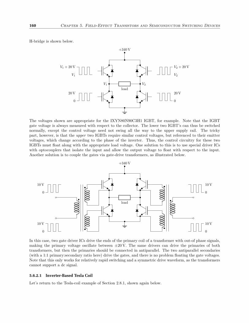
160 Chapter 5. Field-Effect Transistors and Semiconductor Switching Devices
H-bridge is shown below.
+340 V
V1
load
V2
20 V
0
V1
V1 + 20 V
0
20 V
V2 + 20 V
V2
The voltages shown are appropriate for the IXYN80N90C3H1 IGBT, for example. Note that the IGBTgate voltage is always measured with respect to the collector. The lower two IGBT’s can thus be switchednormally, except the control voltage need not swing all the way to the upper supply rail. The trickypart, however, is that the upper two IGBTs require similar control voltages, but referenced to their emittervoltages, which change according to the phase of the inverter. Thus, the control circuitry for these twoIGBTs must float along with the appropriate load voltage. One solution to this is to use special driver ICswith optocouplers that isolate the input and allow the output voltage to float with respect to the input.Another solution is to couple the gates via gate-drive transformers, as illustrated below.
+340 V
load
10 V
0
0
10 V
10 V
0
0
10 V
In this case, two gate driver ICs drive the ends of the primary coil of a transformer with out-of phase signals,making the primary voltage oscillate between ±20 V. The same drivers can drive the primaries of bothtransformers, but then the primaries should be connected in antiparallel. The two antiparallel secondaries(with a 1:1 primary:secondary ratio here) drive the gates, and there is no problem floating the gate voltages.Note that this only works for relatively rapid switching and a symmetric drive waveform, as the transformerscannot support a dc signal.
5.6.2.1 Inverter-Based Tesla Coil
Let’s return to the Tesla-coil example of Section 2.8.1, shown again below.
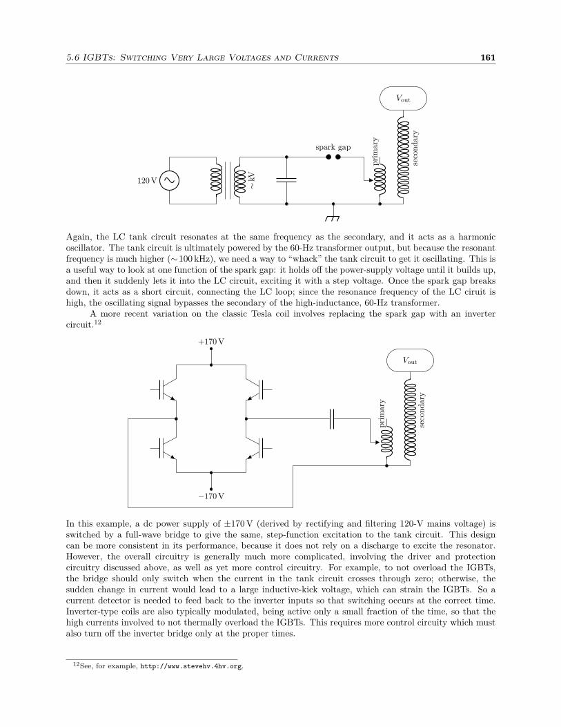
5.6 IGBTs: Switching Very Large Voltages and Currents 161
120 V ∼kV
spark gap
pri
mar
y
seco
ndar
y
Vout
Again, the LC tank circuit resonates at the same frequency as the secondary, and it acts as a harmonicoscillator. The tank circuit is ultimately powered by the 60-Hz transformer output, but because the resonantfrequency is much higher (∼100 kHz), we need a way to “whack” the tank circuit to get it oscillating. This isa useful way to look at one function of the spark gap: it holds off the power-supply voltage until it builds up,and then it suddenly lets it into the LC circuit, exciting it with a step voltage. Once the spark gap breaksdown, it acts as a short circuit, connecting the LC loop; since the resonance frequency of the LC ciruit ishigh, the oscillating signal bypasses the secondary of the high-inductance, 60-Hz transformer.
A more recent variation on the classic Tesla coil involves replacing the spark gap with an invertercircuit.12
−170 V
+170 V
pri
mar
y
seco
ndar
y
Vout
In this example, a dc power supply of ±170 V (derived by rectifying and filtering 120-V mains voltage) isswitched by a full-wave bridge to give the same, step-function excitation to the tank circuit. This designcan be more consistent in its performance, because it does not rely on a discharge to excite the resonator.However, the overall circuitry is generally much more complicated, involving the driver and protectioncircuitry discussed above, as well as yet more control circuitry. For example, to not overload the IGBTs,the bridge should only switch when the current in the tank circuit crosses through zero; otherwise, thesudden change in current would lead to a large inductive-kick voltage, which can strain the IGBTs. So acurrent detector is needed to feed back to the inverter inputs so that switching occurs at the correct time.Inverter-type coils are also typically modulated, being active only a small fraction of the time, so that thehigh currents involved to not thermally overload the IGBTs. This requires more control circuity which mustalso turn off the inverter bridge only at the proper times.
12See, for example, http://www.stevehv.4hv.org.

162 Chapter 5. Field-Effect Transistors and Semiconductor Switching Devices
5.7 Circuit Practice
5.7.1 Touch Switch
Starting in the 1980’s, table lamps with a “touch base” became popular. The idea is, when you touch ametallic base, the lamp toggles between on and off (or between off, on, and two dim states). The key to theoperation of this circuit is that the human body acts as an efficient antenna for 60-Hz radiation, which canbe coupled into a metallic plate (or even a “dangling” wire) and into a circuit. The circuit below shows howthe coupled radiation can be rectified and used as a switch.
1N5711
100 kΩ
1N5711
touch
plate 0.1 µF10 MΩ
50 kΩ
+5 V
1 kΩ
+5 V1 kΩ
+5 V
2N4401BF256B
touch = onno touch = off
• How does this circuit work?
• What is the function of the 10-MΩ resistor?
• Note that Schottky diodes have a small forward voltage (about 0.2 V), to make the circuit moresensitive.
• How would you have to modify the circuit to use a MOSFET in place of the JFET, and can you thinkof an advantage of this circuit over that one?
• To add in some digital electronics, what can you add to the circuit to toggle the LED between ON andOFF on each touch?
• How should this circuit be modified to control a 120-V incandescent lamp?
Solution. When nobody is touching the plate, there is essentially no signal at the input; then the FET isON (the default state), which means the npn base is at low voltage. Thus, the npn transistor is OFF, so theconnection to the LED is pulled to +5 V, so the LED is off. (Strictly, the 1-kΩ resistor at the collector isnot necessary, but it allows the circuit to work if the LED is replaced by something else, such as a relay,discussed below.
When touching the plate, 60-Hz radiation is coupled in, and rectified by the diode network (Schottkydiodes with small forward voltages) to pass only the negative parts of the signal. The first diode (to ground)discards the positive half of the signal, which shouldn’t make it through the second diode anyway; so it seemslike this first diode might not really be necessary. However, this first diode gives a path to ground for thepositive part of the input signal (so the diode network is basically a charge pump, transferring charge fromthe capacitor to ground via the diodes). This process charges the capacitor to negative voltage; when this
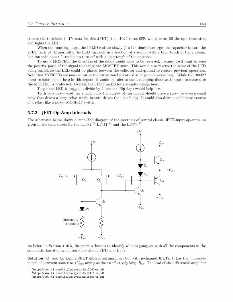
5.7 Circuit Practice 163
crosses the threshold (−4 V max for this JFET), the JFET turns OFF, which turns ON the npn transistor,and lights the LED.
When the touching stops, the 10-MΩ resistor slowly (1-s 1/e time) discharges the capacitor to turn theJFET back ON. Empirically, the LED turns off in a fraction of a second with a brief touch of the antenna,but can take about 2 seconds to turn off with a long tough of the antenna.
To use a MOSFET, the direction of the diode would have to be reversed, because we’d want to keepthe positive parts of the signal to change the MOSFET state. This would also reverse the sense of the LEDbeing on/off, so the LED could be placed between the collector and ground to restore previous operation.Note that MOSFETs are more sensitive to destruction by static discharge and overvoltage. While the 100-kΩinput resistor should help in this regard, it would be safer to use a clamping diode at the gate to make surethe MOSFET is protected. Overall, the JFET makes for a simpler design here.
To get the LED to toggle, a divide-by-2 counter (flip-flop) would help here.To drive a heavy load like a light bulb, the output of this circuit should drive a relay (or even a small
relay that drives a large relay, which in turn drives the light bulp). It could also drive a solid-state versionof a relay, like a power-MOSFET switch.
5.7.2 JFET Op-Amp Internals
The schematic below shows a simplified diagram of the internals of several classic JFET-input op-amps, asgiven in the data sheets for the TL082,13 LF411,14 and the LF353.15
Q1 Q2
+VCC
Q3
D1
−VEE
(internallytrimmed)
−VEE
Vin− Vin+
Q4
Q6
Q5
D2
D3
Vout
−VEE
−VEE
+VCC
+VCC
As before in Section 4.16.5, the exercise here is to identify what is going on with all the components in theschematic, based on what you know about FETs and BJTs.
Solution. Q1 and Q2 form a JFET differential amplifier, but with p-channel JFETs. It has the “improve-ment” of a current source to +VCC, acting as the an effectively large RSS. The load of the differential amplifier
13http://www.ti.com/lit/ds/symlink/tl082-n.pdf14http://www.ti.com/lit/ds/symlink/lf411-n.pdf15http://www.ti.com/lit/ds/symlink/lf353-n.pdf
164 Chapter 5. Field-Effect Transistors and Semiconductor Switching Devices
is a current mirror, here shown as Q3 and D1 (which sets VBE for Q3, and is implemented internally as atransistor as in the usual current mirror in Section 4.11.4. Note that all of the rest of the transistors areBJT’s, to get the high gain desired in an op-amp (recall that JFETs have inherently lower gain comparedto BJT’s because g−1
m tends to be a fair bit larger than re in a comparable device).The two resistors (of the order of a couple kΩ) that appear as a load in addition to the current mirror
allows the voltage offset (i.e., the symmetry of the differential amplifier) to be trimmed. But they alsoimprove the behavior of the current mirror. For example, if they drop something on the order of a coupleof tenths of a volt, they greatly reduce the sensitivity of the current mirror to imbalances in the VBE’s ofthe transistors (due to temperature difference or manufacturing variation). Also according to the Earlyeffect, where VBE varies with VCE, the resistors temper this effect, which would otherwise cause a mismatchof the mirrored current due to varying voltage at the output of this stage. This effectively increases the(differential) output resistance of the current mirror.
The differential amplifier drives a grounded-emitter gain stage (Q4, with a current source as a largeeffective collector resistance RC). A compensation capacitor limits the bandwidth of the op-amp at thisstage. The diodes bias the push-pull complementary emitter-follower pair (Q5 and Q6), which boost thecurrent drive at the output.
Note that because the JFET inputs act as reverse-biased diodes, they can withstand a wide range ofdifferential input voltages. However, they can’t be taken below −VEE, because this would forward-bias theJFET “diodes,” causing them to conduct.
The actual innards of the op-amps are considerably more complicated; detailed diagrams appear inthe data sheets referenced above.
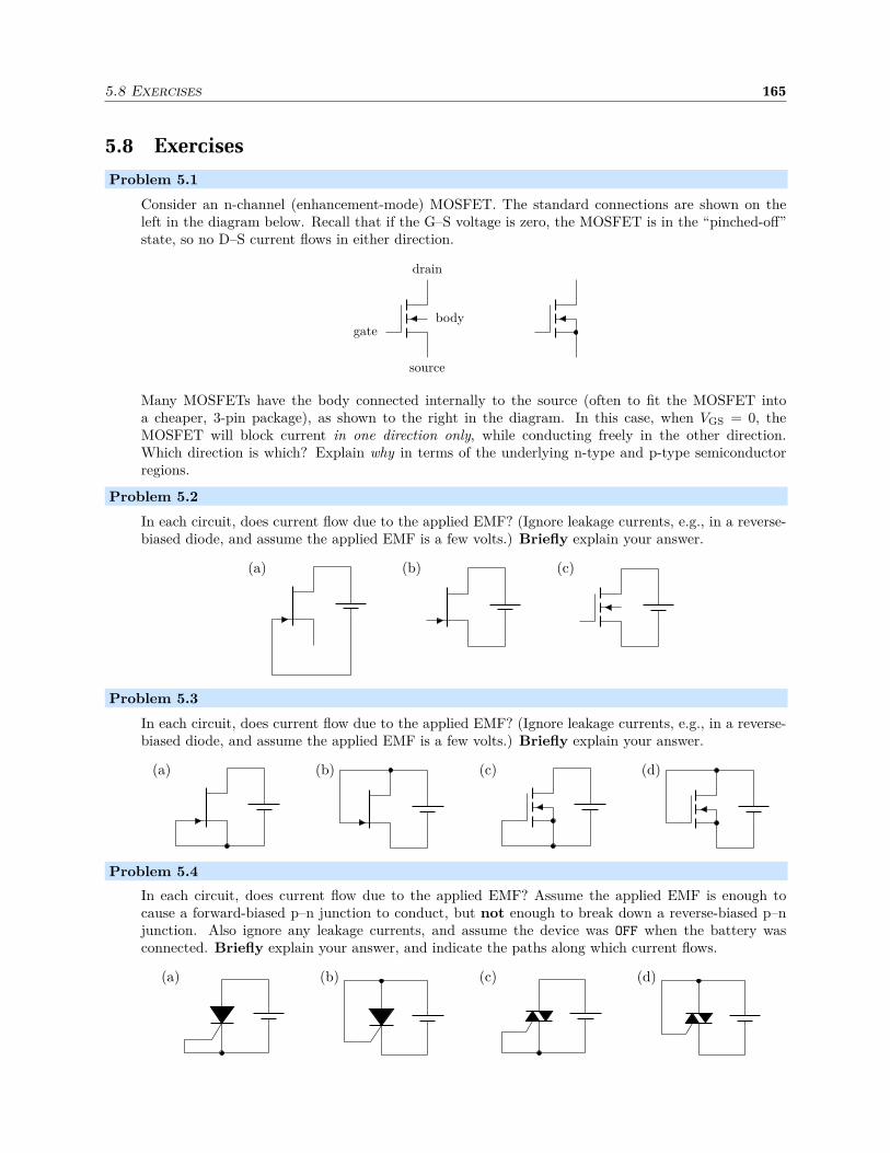
5.8 Exercises 165
5.8 Exercises
Problem 5.1
Consider an n-channel (enhancement-mode) MOSFET. The standard connections are shown on theleft in the diagram below. Recall that if the G–S voltage is zero, the MOSFET is in the “pinched-off”state, so no D–S current flows in either direction.
gate
source
drain
body
Many MOSFETs have the body connected internally to the source (often to fit the MOSFET intoa cheaper, 3-pin package), as shown to the right in the diagram. In this case, when VGS = 0, theMOSFET will block current in one direction only, while conducting freely in the other direction.Which direction is which? Explain why in terms of the underlying n-type and p-type semiconductorregions.
Problem 5.2
In each circuit, does current flow due to the applied EMF? (Ignore leakage currents, e.g., in a reverse-biased diode, and assume the applied EMF is a few volts.) Briefly explain your answer.
(a) (b) (c)
Problem 5.3
In each circuit, does current flow due to the applied EMF? (Ignore leakage currents, e.g., in a reverse-biased diode, and assume the applied EMF is a few volts.) Briefly explain your answer.
(a) (b) (c) (d)
Problem 5.4
In each circuit, does current flow due to the applied EMF? Assume the applied EMF is enough tocause a forward-biased p–n junction to conduct, but not enough to break down a reverse-biased p–njunction. Also ignore any leakage currents, and assume the device was OFF when the battery wasconnected. Briefly explain your answer, and indicate the paths along which current flows.
(a) (b) (c) (d)

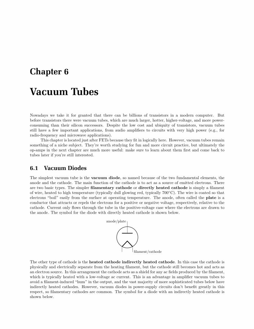
Chapter 6
Vacuum Tubes
Nowadays we take it for granted that there can be billions of transistors in a modern computer. Butbefore transistors there were vacuum tubes, which are much larger, hotter, higher-voltage, and more power-consuming than their silicon successors. Despite the low cost and ubiquity of transistors, vacuum tubesstill have a few important applications, from audio amplifiers to circuits with very high power (e.g., forradio-frequency and microwave applications).
This chapter is located just after FETs because they fit in logically here. However, vacuum tubes remainsomething of a niche subject. They’re worth studying for fun and more circuit practice, but ultimately theop-amps in the next chapter are much more useful: make sure to learn about them first and come back totubes later if you’re still interested.
6.1 Vacuum Diodes
The simplest vacuum tube is the vacuum diode, so named because of the two fundamental elements, theanode and the cathode. The main function of the cathode is to act as a source of emitted electrons. Thereare two basic types. The simpler filamentary cathode or directly heated cathode is simply a filamentof wire, heated to high temperature (typically dull glowing red, typically 700C). The wire is coated so thatelectrons “boil” easily from the surface at operating temperature. The anode, often called the plate is aconductor that attracts or repels the electrons for a positive or negative voltage, respectively, relative to thecathode. Current only flows through the tube in the positive-voltage case where the electrons are drawn tothe anode. The symbol for the diode with directly heated cathode is shown below.
anode/plate
filament/cathode
The other type of cathode is the heated cathode indirectly heated cathode. In this case the cathode isphysically and electrically separate from the heating filament, but the cathode still becomes hot and acts asan electron source. In this arrangement the cathode acts as a shield for any ac fields produced by the filament,which is typically heated with a low-voltage ac current. This is an advantage in amplifier vacuum tubes toavoid a filament-induced “hum” in the output, and the vast majority of more sophisticated tubes below haveindirectly heated cathodes. However, vacuum diodes in power-supply circuits don’t benefit greatly in thisrespect, so filamentary cathodes are common. The symbol for a diode with an indirectly heated cathode isshown below.

168 Chapter 6. Vacuum Tubes
anode/plate
filamentcathode
6.1.1 Child–Langmuir Law
For either cathode type, as the cathode temperature increases, the density of emitted electrons increases,leading to an increased current in forward conduction mode. However this increase does not continueindefinitely: the electrons themselves will modify the electric field between the cathode and anode, and thenet effect is that the current is limited to
I =4ǫ0A
9
√
2e
me
V 3/2
d2. (6.1)
This expression, called the Child–Langmuir Law,1 assumes parallel, identical plates for the anode andcathode, where A is the anode (cathode) area, e is the electron-charge magnitude, me is the electron mass,V is the diode forward voltage, and d is the anode–cathode distance. This scaling of I ∝ V 3/2 holds in othergeometries, but the proportionality factor is geometry-dependent.2 This law can act as a rough guide to thevoltage–current characteristics of a vacuum tube, although it is not accurate enough for quantitative designpurposes. However, it is clear from this law that the turn-on of a vacuum tube with voltage is much less“sudden” than the semiconductor diode, which turns on exponentially with forward voltage.
6.1.2 Vacuum Full-Wave Rectifier
In semiconductor full-wave rectifier circuits, it is typical to use a full-wave bridge consisting of four diodes(see Section 3.6.2). However, vacuum diodes are more complicated and expensive, so such an arrangementis rare. However, to economize on the number of vacuum tubes, a common variation on the vacuum diodeis the vacuum full-wave rectifier. This is the same as a vacuum diode, but with two anodes, forming abridge of two diodes. The schematic symbol is shown below.
anode/plate 1 anode/plate 2
filament/cathode
A common, low-power rectifier tube is the 5Y3, a directly heated full-wave rectifier. The part number inthis case has a typical numbering that is happily informative: the “5” says the filament operates at 5 V, andthe trailing “3” says that there are three elements (two anodes and one cathode). The “Y” is a symbol todifferentiate the tube. The part is often listed as, for example, 5Y3GT, where the “GT” indicates a “glasstube” envelope. The 5Y3 operates with 2 A of filament current, can stand off 1400 V of reverse voltage, andcan handle 400 mA max forward current (in steady state, rising to 2.5 A max transient current). In typical
1C. D. Child, “Discharge From Hot CaO,” Physical Review (Series I), 32, 492 (1911) (doi: 10.1103/PhysRevSeriesI.32.492);Irving Langmuir, “The Effect of Space Charge and Residual Gases on Thermionic Currents in High Vacuum,” Physical Review2, 450 (1913) (doi: 10.1103/PhysRev.2.450).
2For example, for long. coaxial cylinders, the relation becomes I = (8πǫ0L/9)√
2e/meV 3/2/rβ2, where L is the cylinderlength, V is the potential at the radius r, and β is a dimensionless factor of order unity. See Irving Langmuir and Katharine B.Blodgett, “Currents Limited by Space Charge between Coaxial Cylinders,” Physical Review 22, 347 (1923) (doi: 10.1103/Phys-Rev.22.347).
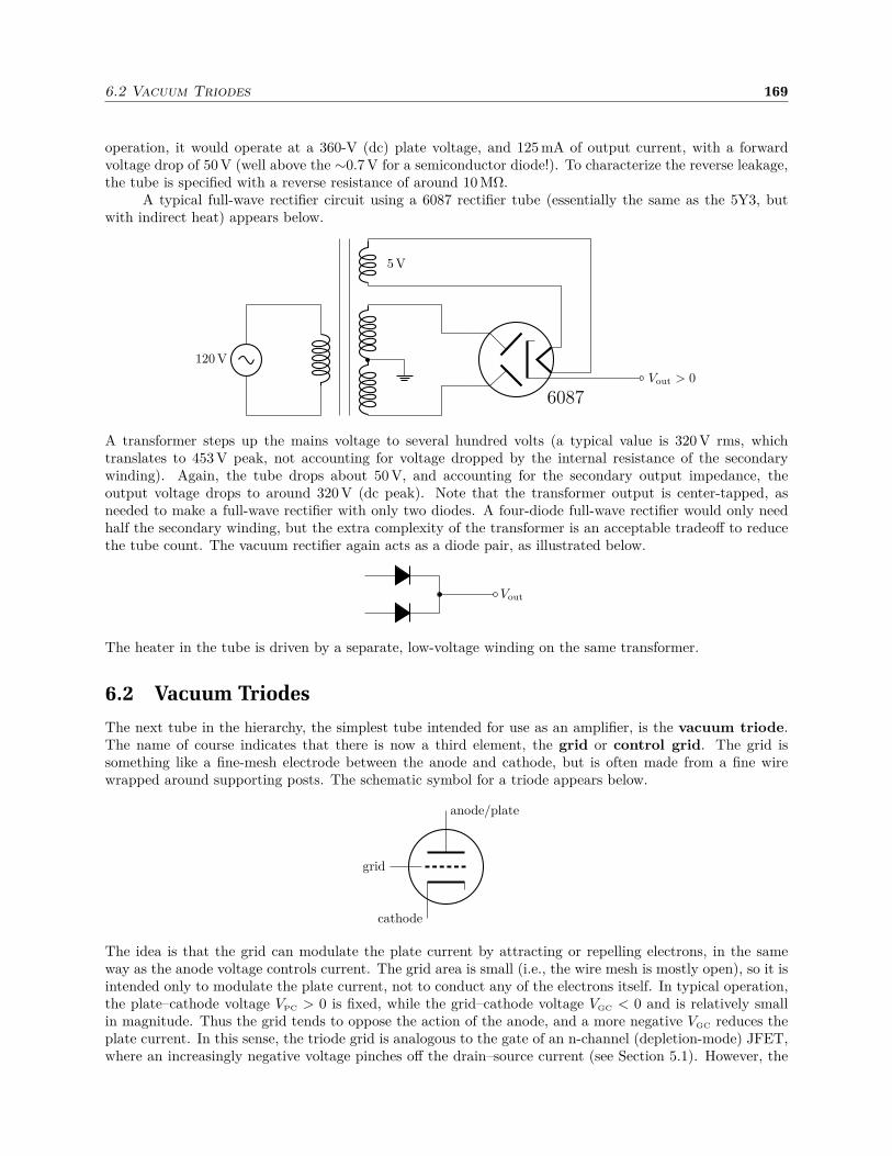
6.2 Vacuum Triodes 169
operation, it would operate at a 360-V (dc) plate voltage, and 125 mA of output current, with a forwardvoltage drop of 50 V (well above the ∼0.7 V for a semiconductor diode!). To characterize the reverse leakage,the tube is specified with a reverse resistance of around 10 MΩ.
A typical full-wave rectifier circuit using a 6087 rectifier tube (essentially the same as the 5Y3, butwith indirect heat) appears below.
Vout > 0
120 V
5 V
6087
A transformer steps up the mains voltage to several hundred volts (a typical value is 320 V rms, whichtranslates to 453 V peak, not accounting for voltage dropped by the internal resistance of the secondarywinding). Again, the tube drops about 50 V, and accounting for the secondary output impedance, theoutput voltage drops to around 320 V (dc peak). Note that the transformer output is center-tapped, asneeded to make a full-wave rectifier with only two diodes. A four-diode full-wave rectifier would only needhalf the secondary winding, but the extra complexity of the transformer is an acceptable tradeoff to reducethe tube count. The vacuum rectifier again acts as a diode pair, as illustrated below.
Vout
The heater in the tube is driven by a separate, low-voltage winding on the same transformer.
6.2 Vacuum Triodes
The next tube in the hierarchy, the simplest tube intended for use as an amplifier, is the vacuum triode.The name of course indicates that there is now a third element, the grid or control grid. The grid issomething like a fine-mesh electrode between the anode and cathode, but is often made from a fine wirewrapped around supporting posts. The schematic symbol for a triode appears below.
anode/plate
grid
cathode
The idea is that the grid can modulate the plate current by attracting or repelling electrons, in the sameway as the anode voltage controls current. The grid area is small (i.e., the wire mesh is mostly open), so it isintended only to modulate the plate current, not to conduct any of the electrons itself. In typical operation,the plate–cathode voltage VPC > 0 is fixed, while the grid–cathode voltage VGC < 0 and is relatively smallin magnitude. Thus the grid tends to oppose the action of the anode, and a more negative VGC reduces theplate current. In this sense, the triode grid is analogous to the gate of an n-channel (depletion-mode) JFET,where an increasingly negative voltage pinches off the drain–source current (see Section 5.1). However, the
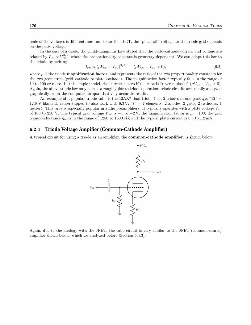
170 Chapter 6. Vacuum Tubes
scale of the voltages is different, and, unlike for the JFET, the “pinch-off” voltage for the triode grid dependson the plate voltage.
In the case of a diode, the Child–Langmuir Law stated that the plate–cathode current and voltage are
related by IPC ∝ V3/2
PC , where the proportionality constant is geometry-dependent. We can adapt this law tothe triode by writing
IPC ∝ (µVGC + VPC)3/2 (µVGC + VPC > 0), (6.2)
where µ is the triode magnification factor, and represents the ratio of the two proportionality constants forthe two geometries (grid–cathode to plate–cathode). The magnification factor typically falls in the range of10 to 100 or more. In this simple model, the current is zero if the tube is “reverse-biased” (µVGC + VPC < 0).Again, the above triode law only acts as a rough guide to triode operation; triode circuits are usually analyzedgraphically or on the computer for quantitatively accurate results.
An example of a popular triode tube is the 12AX7 dual triode (i.e., 2 triodes in one package; “12” =12.6-V filament, center-tapped to also work with 6.3 V; “7” = 7 elements: 2 anodes, 2 grids, 2 cathodes, 1heater). This tube is especially popular in audio preamplifiers. It typically operates with a plate voltage VPC
of 100 to 250 V. The typical grid voltage VGC is −1 to −2 V; the magnification factor is µ = 100; the gridtransconductance gm is in the range of 1250 to 1600 µ; and the typical plate current is 0.5 to 1.2 mA.
6.2.1 Triode Voltage Ampifier (Common-Cathode Amplifier)
A typical circuit for using a triode as an amplifier, the common-cathode amplifier, is shown below.
RP
+VPP
vout
C
vin
RG
RC
Again, due to the analogy with the JFET, the tube circuit is very similar to the JFET (common-source)amplifier shown below, which we analyzed before (Section 5.4.3).

6.2 Vacuum Triodes 171
RS
C
vin
RG
RD
+VDD
vout
In both cases, the grid/gate is biased at 0 V, and the cathode/source resistor functions to elevate the cath-ode/source voltage so the grid gate is biased slightly negative with respect to the cathode/source. In thevacuum-tube case, this is called a cathode-biased amplifier.
The common-cathode amplifier will generally also drive a load, which we can regard as having aThévenin resistance RL. The net effect is that RP should be replaced by RP‖RL, and the supply voltage VPP
should be replaced by the appropriate linear combination of the supply voltage and the Thévenin voltage ofthe load. By using RP and VPP, the following analysis also handles a loaded amplifier if these modificationsare kept in mind.
6.2.1.1 DC Bias
As an example of tube-amplifier analysis, we will work through the analysis of the triode amplifier here. Theplate power supply +VPP, powers the arrangement, supplies plate–cathode current, and as a result it againsets up the bias voltage for the grid. In traditional lingo, the plate power supply is called the “B+ voltage,”in reference to the three elements A, B, and C of the triode (“A” being the cathode and “C” being the grid),and the A, B, and C batteries that were used to power the early circuits.
To begin, the dc current is determined by the power-supply voltage, which must be dropped acrossthe plate and cathode resistors as well as the tube itself along the plate–cathode path:
VPP − VPC = IPC(RP + RC). (6.3)
This is called a “load-line equation,” because when written as a relation for the the plate current IPC as afunction of the plate–cathode voltage VPC, this becomes the equation for a line with slope −1/(RP + RC)and intercept VPP/(RP + RC):
IPC =VPP − VPC
RP + RC
. (6.4)
This current then determines the grid bias point via
VGC = −VC = −IPCRC. (6.5)
Finally, the tube itself has a response current IPC(VGC, VPC) to the grid and plate voltages. In general, thisresponse function does not have a simple form, so the design is often done graphically on a plot of IPC vs.VPC for various values of VGC. The load line and grid-bias relations are superimposed on this plot, and theintersection of the two determines the operating point. However, we can do this using the Child–LangmuirLaw (6.2) to illustrate the process algebraically (at the cost of accuracy):
IPC = a(µVGC + VPC)3/2. (6.6)
Using Eqs. (6.3) and (6.5) to eliminate the voltages, the result is
IPC = a[
VPP −[
(µ + 1)RC + RP
]
IPC
]3/2
. (6.7)
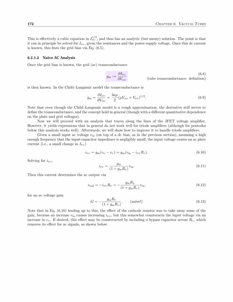
172 Chapter 6. Vacuum Tubes
This is effectively a cubic equation in I1/3PC , and thus has an analytic (but messy) solution. The point is that
it can in principle be solved for IPC, given the resistances and the power-supply voltage. Once this dc currentis known, this fixes the grid bias via Eq. (6.5).
6.2.1.2 Naïve AC Analysis
Once the grid bias is known, the grid (ac) transconductance
gm :=∂IPC
∂VGC
(6.8)(tube transconductance: definition)
is then known. In the Child–Langmuir model the transconductance is
gm =∂IPC
∂VGC
=3aµ
2(µVGC + VPC)1/2. (6.9)
Note that even though the Child–Langmuir model is a rough approximation, the derivative still serves todefine the transconductance, and the concept hold in general (though with a different quantitative dependenceon the plate and grid voltages).
Now we will proceed with an analysis that traces along the lines of the JFET voltage amplifier.However, it yields expressions that in general do not work well for triode amplifiers (although for pentodesbelow this analysis works well). Afterwards, we will show how to improve it to handle triode amplifiers.
Given a small input ac voltage vin (on top of a dc bias, as in the previous section), assuming a highenough frequency that the input-capacitor impedance is negligibly small, the input voltage causes an ac platecurrent (i.e., a small change in IPC)
iPC = gm(vG − vC) = gm(vin − iPCRC). (6.10)
Solving for iPC,
iPC =gm
(1 + gmRC)vin. (6.11)
Then this current determines the ac output via
vout = −iPCRP = − gmRP
(1 + gmRC)vin, (6.12)
for an ac voltage gain
G = − gmRP
(1 + gmRC). (naïve!) (6.13)
Note that in Eq. (6.10) leading up to this, the effect of the cathode resistor was to take away some of thegain, because an increase vin causes increasing iPC, but this somewhat counteracts the input voltage via anincrease in vC. If desired, this effect may be counteracted by including a bypass capacitor across RC, whichremoves its effect for ac signals, as shown below.
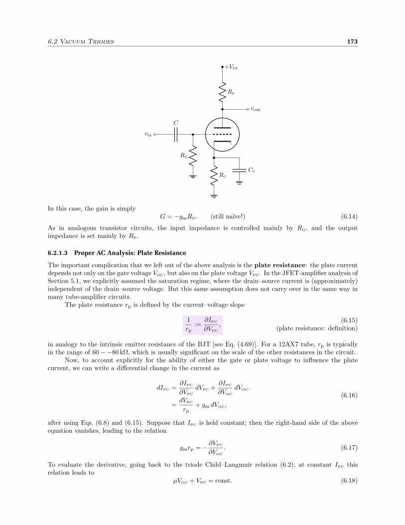
6.2 Vacuum Triodes 173
RP
+VPP
vout
C
vin
RG
RC
CC
In this case, the gain is simplyG = −gmRP. (still naïve!) (6.14)
As in analogous transistor circuits, the input impedance is controlled mainly by RG, and the outputimpedance is set mainly by RP.
6.2.1.3 Proper AC Analysis: Plate Resistance
The important complication that we left out of the above analysis is the plate resistance: the plate currentdepends not only on the gate voltage VGC, but also on the plate voltage VPC. In the JFET-amplifier analysis ofSection 5.1, we explicitly assumed the saturation regime, where the drain–source current is (approximately)independent of the drain–source voltage. But this same assumption does not carry over in the same way inmany tube-amplifier circuits.
The plate resistance rp is defined by the current–voltage slope
1
rp:=
∂IPC
∂VPC
,(6.15)
(plate resistance: definition)
in analogy to the intrinsic emitter resistance of the BJT [see Eq. (4.69)]. For a 12AX7 tube, rp is typicallyin the range of 60−−80 kΩ, which is usually significant on the scale of the other resistances in the circuit.
Now, to account explicitly for the ability of either the gate or plate voltage to influence the platecurrent, we can write a differential change in the current as
dIPC =∂IPC
∂VPC
dVPC +∂IPC
∂VGC
dVGC
=dVPC
rp+ gm dVGC,
(6.16)
after using Eqs. (6.8) and (6.15). Suppose that IPC is held constant; then the right-hand side of the aboveequation vanishes, leading to the relation
gmrp = −∂VPC
∂VGC
. (6.17)
To evaluate the derivative, going back to the triode Child–Langmuir relation (6.2), at constant IPC thisrelation leads to
µVGC + VPC = const. (6.18)
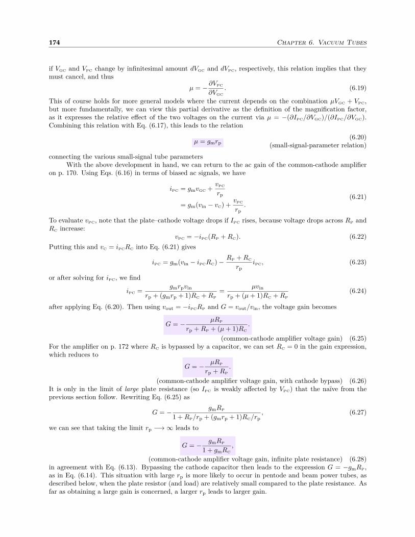
174 Chapter 6. Vacuum Tubes
if VGC and VPC change by infinitesimal amount dVGC and dVPC, respectively, this relation implies that theymust cancel, and thus
µ = −∂VPC
∂VGC
. (6.19)
This of course holds for more general models where the current depends on the combination µVGC + VPC,but more fundamentally, we can view this partial derivative as the definition of the magnification factor,as it expresses the relative effect of the two voltages on the current via µ = −(∂IPC/∂VGC)/(∂IPC/∂VGC).Combining this relation with Eq. (6.17), this leads to the relation
µ = gmrp(6.20)
(small-signal-parameter relation)
connecting the various small-signal tube parametersWith the above development in hand, we can return to the ac gain of the common-cathode amplifier
on p. 170. Using Eqs. (6.16) in terms of biased ac signals, we have
iPC = gmvGC +vPC
rp
= gm(vin − vC) +vPC
rp.
(6.21)
To evaluate vPC, note that the plate–cathode voltage drops if IPC rises, because voltage drops across RP andRC increase:
vPC = −iPC(RP + RC). (6.22)
Putting this and vC = iPCRC into Eq. (6.21) gives
iPC = gm(vin − iPCRC)− RP + RC
rpiPC, (6.23)
or after solving for iPC, we find
iPC =gmrpvin
rp + (gmrp + 1)RC + RP
=µvin
rp + (µ + 1)RC + RP
(6.24)
after applying Eq. (6.20). Then using vout = −iPCRP and G = vout/vin, the voltage gain becomes
G = − µRP
rp + RP + (µ + 1)RC
.
(common-cathode amplifier voltage gain) (6.25)For the amplifier on p. 172 where RC is bypassed by a capacitor, we can set RC = 0 in the gain expression,which reduces to
G = − µRP
rp + RP
.
(common-cathode amplifier voltage gain, with cathode bypass) (6.26)It is only in the limit of large plate resistance (so IPC is weakly affected by VPC) that the naïve from theprevious section follow. Rewriting Eq. (6.25) as
G = − gmRP
1 + RP/rp + (gmrp + 1)RC/rp, (6.27)
we can see that taking the limit rp −→∞ leads to
G = − gmRP
1 + gmRC
,
(common-cathode amplifier voltage gain, infinite plate resistance) (6.28)in agreement with Eq. (6.13). Bypassing the cathode capacitor then leads to the expression G = −gmRP,as in Eq. (6.14). This situation with large rp is more likely to occur in pentode and beam power tubes, asdescribed below, when the plate resistor (and load) are relatively small compared to the plate resistance. Asfar as obtaining a large gain is concerned, a larger rp leads to larger gain.

6.2 Vacuum Triodes 175
6.2.2 Design Example: 12AX7 Preamplifier
As a specific example, consider a preamplifier stage made from (half of) a 12AX7, with
• RP = 100 kΩ,
• RC = 1.5 kΩ,
• RG = 1 MΩ (the grid resistor only really matters for the input impedance and to ensure a proper gridbias),
• VPP = 330 V, and
• model values of a = 1.89× 10⁻⁶ A/V3/2 and µ = 100 for the 12AX7 (see the next section),
a numerical solution of Eq. (6.7) yieldsIPC ≈ 1.04 mA, (6.29)
which leads to a grid bias from Eq. (6.5) of
VGC = −1.57 V, (6.30)
a tube plate–cathode voltage from Eq. (6.3) of
VPC = 224 V, (6.31)
and a grid transconductance from Eq. (6.9) of
gm = 2330 µ. (6.32)
Note that the transconductance falls above the range quoted for the 12AX7 in the first part of Section 6.2.With µ = 100 by assumption and
rp = µ/gm = 43.0 kΩ (6.33)
from Eq. (6.20), the amplifier gain isG = −34, (6.34)
from Eq. (6.25) [G = −52 from the naïve expression (6.13)], or if the cathode resistor is bypassed, the gainis
G = −70 (6.35)
[G = 233 from the naïve expression (6.14)]. Again, these values should not be taken too seriously, given thesimple Child–Langmuir model, although we will see below that they aren’t too bad in this example.
6.2.3 Phenomenological Triode Model
It is possible to model the triode behavior more accurately than via the Child–Langmuir model. Koren, forexample, proposed the following phenomenological model for a triode:3
V1 =VPC
kP
log
1 + exp
[
kP
(
µ−1 +VGC
√
kVB + V 2PC
)]
IPC =V x
1
kG
[
1 + sgn(V1)]
.
(6.36)
Note that when V 2PC≫ kVB, kP(µ−1 + VGC/VPC) ≫ 1, and x = 3/2, these equations reduce to the Child–
Langmuir Law (6.6) in the form IPC = (VPC/µ + VGC)3/22/kG, so that we can identify a = 2/kGµ3/2.
3Norman L. Koren, “Improved vacuum tube models for SPICE simulations. Part 1: Models and example,” http://www.
normankoren.com/Audio/Tubemodspice_article.html (update 2003).
176 Chapter 6. Vacuum Tubes
Koren’s parameters for the 12AX7 read as follows:
µ = 100
kG = 1060 Vx/A
kP = 600 V
kVB = 300√
V
x = 1.4.
(6.37)
Then solving Eqs. (6.36) numerically, along with the load-line equation (6.4) and the grid-bias equation (6.5),we find
IPC = 1.07 mA
VPC = 221 V
VGC = −1.61 V.
(6.38)
To “seed” the root-finding process, the Child–Langmuir results from the previous section may be used asinitial guesses. While the previous results are fairly close (they were within a few percent of these values),it is evident that using the better model makes a difference in the design results. Now the transconductancefollows from differentiating Eqs. (6.36),
gm =∂IPC
∂VGC
= 1880 µ, (6.39)
and Eq. (6.20) gives
rp =µ
gm= 53.3 kΩ, (6.40)
which is somewhat low compared to the RCA specification4 Eq. (6.25) then leads to a circuit gain of
G = −33 (6.41)
with the feedback from RC, orG = −65 (6.42)
with RC bypassed. The Child–Langmuir versions of the gain values were more than 10% from the correctvalues.
So is this accuracy typical for the Child–Langmuir model? To see this, and to also see how to do thiscalculation graphically (in case only graphical tube data are available from a data sheet), the plot belowshows the plate IPC–VPC characteristics for various gate voltages, shown as the solid curves (from the Korenmodel). The accompanying dashed curves show the Child–Langmuir predictions by comparison; note thatthese agree in some regions, but not in others.
4Available at http://drtube.com/datasheets/12ax7-rca1962.pdf, see the plot on the last page.
6.3 Vacuum Tetrodes 177
VPC (V)0 400100 200 300
IPC (
mA
)
5
0
1
2
3
4
VGCo=
o0oV
-0.5oV
-1.0oV
-1.5oV
-2.0oV
-2.5oV
-3.0oV
12AX7
load line
grid bias
oper
atin
g po
int
To solve this system, the next step is to draw in the load line (6.3), which is independent of any tubecharacteristics. Then, draw in the grid-bias curve (6.5) by drawing the point on each curve of constant VGC
that satisfies Eq. (6.5) (i.e., by tracing along the curve to the proper current IPC = −VGC/RC). Then theidea is to fill in the curve; while it is not a straight line, a straight line is a reasonably good approximationnear any point. The intersection of the load line and the grid-bias curve determine the (dc) operating pointof the circuit, and the slope of the grid-bias curve at the operating point gives the transconductance gm.Alternately, it is possible to more directly obtain the ac amplifier gain, in the case of a bypassed RC: acchanges in the grid voltage don’t affect the bias, so one can follow the load line to find the change in IPC fora change in VGC, and convert to a gain via RP.
From this diagram it is evident that the circuit happens to operate in the region where the Child–Langmuir model works reasonably well. For tubes in a push–pull circuit, which operate near zero currentwhen the output signal crosses through zero, the simple model makes for a much poorer approximation. Notethat the model (6.36) is not perfect either: compared to the RCA data sheet, for example,5 the VGC = 0curve has a “kink” with the opposite curvature for small VPC. However, this model is probably reasonablefor estimates in practical designs.
6.3 Vacuum Tetrodes
While the triode can work well, it has an issue, the Miller capacitance between the plate and grid. Thisis analogous to the Miller effect in bipolar transistors that we mentioned before in Section 4.11.5.3, but ofcourse the vacuum-tube version came first. The Miller capacitance can cause a loss of bandwidth, but evenworse, it can cause instability in high-gain circuits, because it acts as a feedback coupling between the high-current output and the sensitive input of an amplifier stage. One solution to this was to introduce a secondgrid, called the screen grid (also called grid #2, with the control grid going by the cheeky alternativegrid #1). The resulting tube is the tetrode, in reference to the fourth element. The schematic symbol forthe tetrode is shown below.
anode/plate
control grid (grid #1)screen grid (grid #2)
cathode
5http://www.r-type.org/pdfs/12ax7.pdf

178 Chapter 6. Vacuum Tubes
The screen grid sits between the plate and the control grid. The idea is to have a positive, fixed potential ofthe screen grid, VG2C > 0, but still negative with respect to the plate (VG2C < VPC). Typically this voltage isset via a voltage divider from the plate voltage, and is preferably also bypassed to ground with a capacitor.The control grid is still biased negative (VG1C < 0). Since the screen grid is at fixed potential, it acts asa shield (hence the name “screen,” in reference to electrical screening), breaking the capacitive couplingbetween plate and control grid. The new grid can reduce the control-grid–plate capacitance from several pFto below 0.01 pF.
Since VG2C > 0, the screen grid also attracts electrons from the cathode, which we will see can be aproblem. However, this has an advantage, since the screen grid shields somewhat the effect of the anode onthe cathode electrons. The net effect is that the plate current IPC is relatively insensitive to the plate voltageVPC (for sufficiently large VPC), which can be a useful property.
6.4 Vacuum Pentodes and Beam Power Tubes
The tetrode, alas, has yet another problem, related to secondary emission, which is the emission ofelectrons from the anode due to cathode electrons striking it. In diodes and triodes, secondary-emissionelectrons are simply attracted back to the anode, and so don’t affect things much (except through space-charge effects). However, in tetrodes, the secondary electrons are attracted to the screen, especially if thescreen grid is biased above the plate. The net effect is the reduce the plate current and overall gain of thecircuit, and it reduces the useful range of VPC.
The solution is to add yet another grid, the suppressor grid or grid #3, forming the pentode. Thesuppressor grid site between the screen grid and plate; usually it is shorted to the cathode, and it functionsto repel secondary electrons. The pentode diagram is shown below.
anode/plate
control grid (grid #1)screen grid (grid #2)
suppressor grid (grid #3)
cathode
The design of tetrode and pentode circuits is essentially the same as in triode circuits, with the extracomplication of the additional freedom of choosing extra grid voltages, and of more complicated mathematicalmodels for the tube characteristics.
An alternative solution to the suppressor grid comes in the beam power tube. This is generally; apentode, with grid #3 replaced by a beam-forming electrode. (Confusingly, data sheets can refer to thesame beam power tubes as tetrodes or pentodes.) The schematic symbol appears below.
anode/plate
control grid (grid #1)screen grid (grid #2)
cathode
beam-forming electrode
Like the suppressor grid, the beam-forming electrode is typically shorted to the cathode, and serves to directthe cathode electrons in a beam onto a particular part of the plate. Because of the controlled electron impacton the plate, such tubes can handle high currents. It also serves to suppress secondary electrons in the sameway as the suppressor grid. Famous examples of beam power tubes are the 6V6 at lower powers and the6L6 at somewhat higher powers (“6” = 6 elements: cathode, heater, plate, control grid, screen grid, beam-forming electrode). For comparison to the 12AX7 preamplifier tube, the 6V6 in typical operattion has a
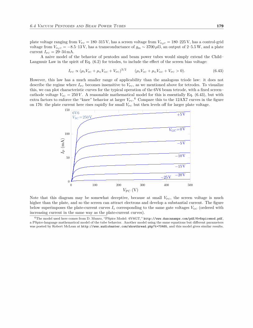
6.4 Vacuum Pentodes and Beam Power Tubes 179
plate voltage ranging from VPC = 180–315 V, has a screen voltage from VG2C = 180–225 V, has a control-gridvoltage from VG1C = −8.5–13 V, has a transconductance of gm ∼ 3700 µ, an output of 2–5.5 W, and a platecurrent IPC = 29–34 mA.
A naive model of the behavior of pentodes and beam power tubes would simply extend the Child–Langmuir Law in the spirit of Eq. (6.2) for triodes, to include the effect of the screen bias voltage:
IPC ∝ (µSVSC + µGVGC + VPC)3/2 (µSVSC + µGVGC + VPC > 0). (6.43)
However, this law has a much smaller range of applicability than the analogous triode law: it does notdescribe the regime where IPC becomes insensitive to VPC, as we mentioned above for tetrodes. To visualizethis, we can plot characteristic curves for the typical operation of the 6V6 beam tetrode, with a fixed screen–cathode voltage VSC = 250 V . A reasonable mathematical model for this is essentially Eq. (6.43), but withextra factors to enforce the “knee” behavior at larger VPC.6 Compare this to the 12AX7 curves in the figureon 176: the plate current here rises rapidly for small VPC but then levels off for larger plate voltage.
VPC (V)0 500100 200 300 400
IP (
mA
)
150
0
100
50
+5oV
VGCo=o0oV
-5oV
-10oV
-15oV
-20oV-25oV
6V6VSCo=o250oV
Note that this diagram may be somewhat deceptive, because at small VPC, the screen voltage is muchhigher than the plate, and so the screen can attract electrons and develop a substantial current. The figurebelow superimposes the plate-current curves IS corresponding to the same gate voltages VGC (ordered withincreasing current in the same way as the plate-current curves).
6The model used here comes from D. Munro, “PSpice Model: 6V6GT,” http://www.duncanamps.com/pdf/6v6spicemod.pdf,a PSpice-language mathematical model of the tube behavior. Another model using the same equations but different parameterswas posted by Robert McLean at http://www.audiobanter.com/showthread.php?t=70465, and this model gives similar results.
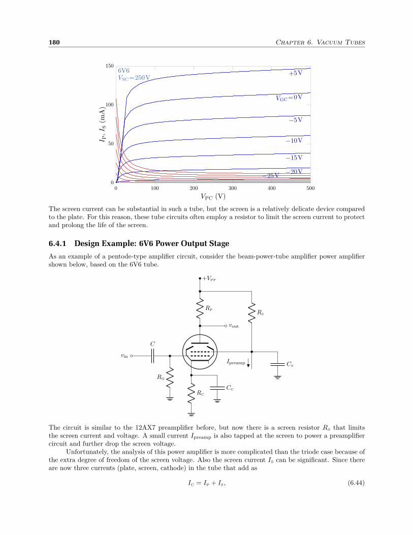
180 Chapter 6. Vacuum Tubes
VPC (V)0 500100 200 300 400
I P,I S
(m
A)
150
0
100
50
+5oV
VGCo=o0oV
-5oV
-10oV
-15oV
-20oV-25oV
6V6VSCo=o250oV
The screen current can be substantial in such a tube, but the screen is a relatively delicate device comparedto the plate. For this reason, these tube circuits often employ a resistor to limit the screen current to protectand prolong the life of the screen.
6.4.1 Design Example: 6V6 Power Output Stage
As an example of a pentode-type amplifier circuit, consider the beam-power-tube amplifier power amplifiershown below, based on the 6V6 tube.
RP
+VPP
vout
C
vin
RG
RC
CC
RS
Ipreamp CS
The circuit is similar to the 12AX7 preamplifier before, but now there is a screen resistor RS that limitsthe screen current and voltage. A small current Ipreamp is also tapped at the screen to power a preamplifiercircuit and further drop the screen voltage.
Unfortunately, the analysis of this power amplifier is more complicated than the triode case because ofthe extra degree of freedom of the screen voltage. Also the screen current IS can be significant. Since thereare now three currents (plate, screen, cathode) in the tube that add as
IC = IP + IS, (6.44)

6.4 Vacuum Pentodes and Beam Power Tubes 181
the load-line graphical analysis is more complicated because the voltage drops across RP and RC arise dueto different currents:
VPP − VPC = IPRP + ICRC. (6.45)
This leads to a load “line” which isn’t a line anymore, because IS is not simply related to IP:
VPP − IPRP − ICRC = VPC. (6.46)
Further, IS determines the ground-referenced screen voltage via
VS = VPP − (IS + Ipreamp)RS, (6.47)
but the screen–cathode voltage is also determined by the cathode bias:
VSC = VS − ICRC. (6.48)
We still have the plate and control-grid bias voltages, as in the triode case:
VPC = VP − ICRC
VGC = −ICRC.(6.49)
This leads to a relatively complicated coupled system of equations. The graphical analysis in particular iscomplicated by the need to consult graphs of both the plate and cathode currents to even set the properbias. In practice, crude approximations such as assuming IS to be a fixed fraction of IC are sufficient forapproximate design work. But if a mathematical model of the tube is available, it is more convenientnowadays to let a compute grind out the numerical solution of these equations.
As an example, suppose we assume the following parameter set:
• RP = 284.2 Ω (i.e., the dc resistance of the primary coil of an output transformer),
• RC = 470 Ω,
• RS = 1 kΩ,
• RG = 220 kΩ (again, the grid resistor only really matters for the input impedance and to tie the gridto ground; the grid current is negligible provided it is biased negative with respect to the cathode),
• VPP = 360 V, and
• Ipreamp = 2 mA to power a small preamplifier.
The numerical solution to the above equations, including the 6V6 model, gives
IP = 43.6 mA
IS = 3.75 mA
IC = 47.3 mA
VPC = 325 V
VGC = −22.2 V
VS = 354 V
VP = 347 V.
(6.50)
To check the tube operation, these results imply power dissipations of
PP = VPCIP = 14.2 W
PP = VSCIS = 1.25 W(6.51)

182 Chapter 6. Vacuum Tubes
at the plate and screen, respectively. The 6V6 has specified maximum powers of 12 W and 2 W, respectively,so this design is pushing the limits of the plate power. (If the plate power exceeds the specification by toomuch, the tube will “red plate,” or the anode will glow red with heat, dramatically shortening the tube’slife.)
All this and more is illustrated in the plot below. The characteristic curves for this arrangementare shown as solid curves; the dashed curves show the corresponding characteristics when VSC is held at aconstant 330 V, illustrating the importance of numerically solving for the correct VSC in the analysis.
VPC (V)0 500100 200 300 400
IP (
mA
)
100
50
0
VGCo=o-10oV
-15oV
-20oV
-25oV
-30oV
-35oV
6V6RSo=o1okW,VPPo=o360oVRCo=o470oW,Ipreampo=o2omA
load lin
eac load line
grid bias
operating point
The (dc) load curve is plotted from Eq. (6.46); the dashed counterpart is the load line obtained by ignoringthe small contribution of IS. Clearly the screen current makes a difference, but here it doesn’t change muchto ignore it.
The grid-bias curve is more difficult to construct graphically here because it only intersects one char-acteristic curve (for VGC = −20 V). The plotted points are separated by ∆VGC = 0.1 V, from VGC = −19 V to−22.5 V, from left to right. Recall that this curve is determined by the cathode current, which is determinedby the plate and screen voltages. The intersection with the load line again gives the operation point.
A different, ac load line is also shown. Since RP corresponds to the primary winding of an outputtransformer, it has a different ac response than the dc resistance. The plotted curve assumes a nominalac impedance of 7 kΩ. This load line shows how changes to the gate voltage translate into output-currentchanges. Note that if VGC rises much above −10 V, the curves bunch together, resulting in clipping of thesignal; the same is true if VGC goes below −35 V or so.
Computing the ac gain directly is somewhat easier than setting the dc bias, because the bypass ca-pacitors allow us to assume that the cathode voltage VC and screen voltages VS and VSC are fixed. Thetransconductance can be evaluated by numerically differentiating the tube model. The result here is
gm =∂IP
∂VGC
= 4330 µ, (6.52)
which is similar to values specified in the data sheet. The plate resistance then follows from adapting thedefinition (6.15) to read
1
rp:=
∂IP
∂VPC
. (6.53)
This derivative can be evaluated numerically as well, and comes to
rp = 72.5 kΩ. (6.54)
Because of the extra dependence on the screen voltage, the relation gmrp = µ of Eq. (6.20) no longer holdsexactly. For example, the 6V6 model assumes a grid µ of 390 (and a screen µ of 43), but gmrp = 314 fromthe numerical calculations

6.4 Vacuum Pentodes and Beam Power Tubes 183
The ac voltage gain from Eq. (6.26) is then
G = −gmrpZP
rp + ZP
= −27.7, (6.55)
after restoring gmrp in place of µ and taking RP to be the ac impedance ZP. Note that the “naïve” resultG = −gmZP from Eq. (6.14) works reasonably well here, predicting G = −30.3, because the plate resistanceis indeed substantially larger than the plate impedance, by more than a factor of 20. In any case, the gainhere is lower than in the triode preamplifier example.
6.4.2 Triode Connection
The characteristic curves in the triode-amplifier example of Section 6.2.3 appeared quite different from thebeam-power-tetrode example of Section 6.4.1. Roughly speaking the triode is operated in a regime where itbehaves like a variable resistor, controlled by the grid voltage. This is evident in the gain expressions (6.25)and (6.26), where the plate resistance (along with the magnification) determine the tube’s contribution tothe amplifier gain. The pentode-type circuits, however, when the screen is held at a fixed potential, aredifferent: they typically run in a regime with large plate resistance, making the tube output behave morelike a current source (since the plate current is insensitive to VPC). In this regime the tube’s contribution tothe amplifier gain comes in the form of the transconductance, as in Eq. (6.28).
Pentodes (and beam power tubes) work well enough, but sometimes triode characteristics are moredesirable, for example for their distortion or low-noise properties. One common trick for achieving this witha pentode-type tube is the triode connection, where the screen is shorted to the plate (typically this isdone via a resistor of ∼100 Ω, which limits screen current and suppresses high-frequency instabilities).
As an example, consider the same power-amplifier stage as in the previous section, but with a triode-connected 6V6 (with a direct plate–screen short for simplicity). The analysis is essentially the same, exceptEq. (6.47) is replaced by the condition VS = VP. The dc operating point turns out to be nearly the same (allthe values below are within a few percent of the previous values):
IP = 42.7 mA
IS = 3.68 mA
IC = 46.4 mA
VPC = 326 V
VGC = −21.8 V
VS = 348 V
VP = 348 V.
(6.56)
The characteristic curves are shown below, with the same load curves, and the appropriate grid-bias curve.
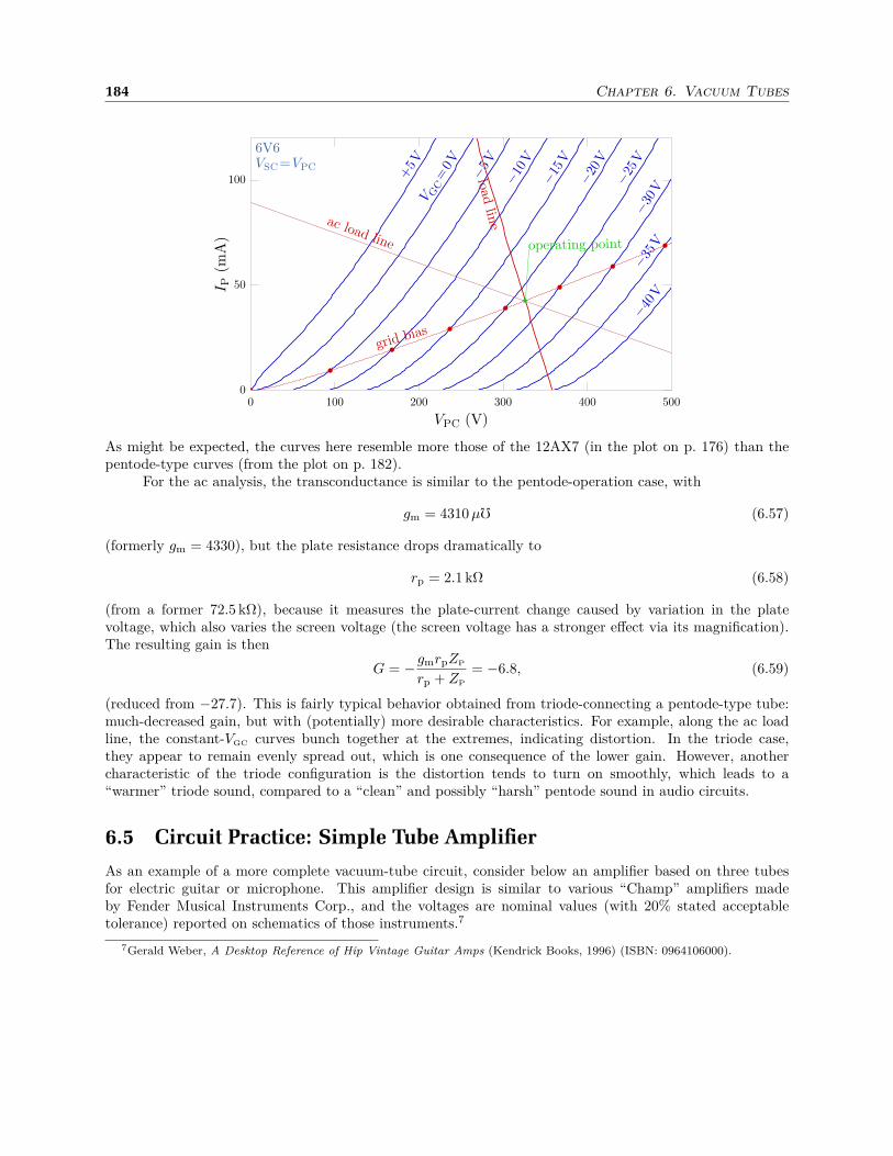
184 Chapter 6. Vacuum Tubes
load lin
e
VPC (V)0 500100 200 300 400
IP (
mA
)
100
50
0+
5oV
V GCo=
o0oV
-5oV
-10oV
-15oV
-20oV
-25oV
-30oV
-35oV
-40
oV
6V6VSCo=oVPC
grid bias
ac load line operating point
As might be expected, the curves here resemble more those of the 12AX7 (in the plot on p. 176) than thepentode-type curves (from the plot on p. 182).
For the ac analysis, the transconductance is similar to the pentode-operation case, with
gm = 4310 µ (6.57)
(formerly gm = 4330), but the plate resistance drops dramatically to
rp = 2.1 kΩ (6.58)
(from a former 72.5 kΩ), because it measures the plate-current change caused by variation in the platevoltage, which also varies the screen voltage (the screen voltage has a stronger effect via its magnification).The resulting gain is then
G = −gmrpZP
rp + ZP
= −6.8, (6.59)
(reduced from −27.7). This is fairly typical behavior obtained from triode-connecting a pentode-type tube:much-decreased gain, but with (potentially) more desirable characteristics. For example, along the ac loadline, the constant-VGC curves bunch together at the extremes, indicating distortion. In the triode case,they appear to remain evenly spread out, which is one consequence of the lower gain. However, anothercharacteristic of the triode configuration is the distortion tends to turn on smoothly, which leads to a“warmer” triode sound, compared to a “clean” and possibly “harsh” pentode sound in audio circuits.
6.5 Circuit Practice: Simple Tube Amplifier
As an example of a more complete vacuum-tube circuit, consider below an amplifier based on three tubesfor electric guitar or microphone. This amplifier design is similar to various “Champ” amplifiers madeby Fender Musical Instruments Corp., and the voltages are nominal values (with 20% stated acceptabletolerance) reported on schematics of those instruments.7
7Gerald Weber, A Desktop Reference of Hip Vintage Guitar Amps (Kendrick Books, 1996) (ISBN: 0964106000).
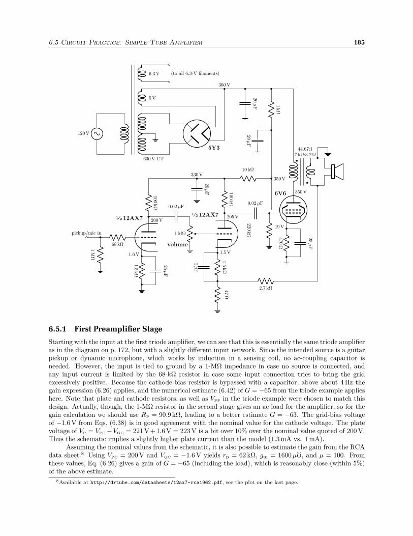
6.5 Circuit Practice: Simple Tube Amplifier 185
1⁄2 12AX7
100kΩ
68 kΩ
1M
Ω
pickup/mic in
1.5kΩ
25µ
F
0.02 µF
1 MΩ
volume
1⁄2 12AX7
100kΩ
1.5kΩ
47Ω
2µ
F
6V6
2.7 kΩ
44.67:17 kΩ:3.2 Ω
0.02 µF
220kΩ
470Ω
25µ
F
120 V
5 V
6.3 V (to all 6.3-V filaments)
5Y3
630 V CT20
µF 1kΩ
20µ
F10 kΩ
20µ
F
360 V
350 V
350 V330 V
200 V205 V
1.6 V 1.5 V
19 V
6.5.1 First Preamplifier Stage
Starting with the input at the first triode amplifier, we can see that this is essentially the same triode amplifieras in the diagram on p. 172, but with a slightly different input network. Since the intended source is a guitarpickup or dynamic microphone, which works by induction in a sensing coil, no ac-coupling capacitor isneeded. However, the input is tied to ground by a 1-MΩ impedance in case no source is connected, andany input current is limited by the 68-kΩ resistor in case some input connection tries to bring the gridexcessively positive. Because the cathode-bias resistor is bypassed with a capacitor, above about 4 Hz thegain expression (6.26) applies, and the numerical estimate (6.42) of G = −65 from the triode example applieshere. Note that plate and cathode resistors, as well as VPP in the triode example were chosen to match thisdesign. Actually, though, the 1-MΩ resistor in the second stage gives an ac load for the amplifier, so for thegain calculation we should use RP = 90.9 kΩ, leading to a better estimate G = −63. The grid-bias voltageof −1.6 V from Eqs. (6.38) is in good agreement with the nominal value for the cathode voltage. The platevoltage of VP = VPC−VGC = 221 V + 1.6 V = 223 V is a bit over 10% over the nominal value quoted of 200 V.Thus the schematic implies a slightly higher plate current than the model (1.3 mA vs. 1 mA).
Assuming the nominal values from the schematic, it is also possible to estimate the gain from the RCAdata sheet.8 Using VPC = 200 V and VGC = −1.6 V yields rp = 62 kΩ, gm = 1600 µ, and µ = 100. Fromthese values, Eq. (6.26) gives a gain of G = −65 (including the load), which is reasonably close (within 5%)of the above estimate.
8Available at http://drtube.com/datasheets/12ax7-rca1962.pdf, see the plot on the last page.

186 Chapter 6. Vacuum Tubes
6.5.2 Second Preamplifier Stage
The second-stage preamplifier, after the volume control, is essentially identical to the first, except for theaddition of the 47-Ω resistor and the feedback path from the output transformer. We will save the feedbackfor later, but the extra resistance yields modified values of VPC = 226 V (vs. 225 V) and VGC = −1.59 V (vs.−1.61 V). Again, these are close to the nominal values. The gain expression (6.25) gives G = −54, usingRP = 68.8 kΩ (including the 220-kΩ input resistor of the power stage) and RC = 47 Ω. The data sheet forthese conditions gives rp = 60 kΩ, gm = 1650 µ, and µ = 101, giving a gain of G = −52.
6.5.3 Power Amplifier Stage
The power-amplifier stage is intended to match the prototype power-amplifier circuit of Section section:6V6amp,including the 1 mA of current that supplies each preamplifier stage. The output transformer acts as a load;the transformer is a Hammond 1750C.9 The primary dc resistance is specified as 284.2 Ω, but can varyconsiderably (one example measured 267 Ω). The transformer specifies an ac impedance ratio of 7000 : 3.2,which means that a 3.2-Ω speaker load appears as a 7-kΩ load at the 6V6 plate. (The ac impedances arenominal values, varying widely with frequency because of the frequency response of the transformer andespecially of the speaker.) The ac gain for this stage is G = −27.7.
6.5.4 Feedback Loop
The main remaining feature of the circuit, besides the power supply, is the 2.7-kΩ resistor connecting thetransformer secondary to the cathode resistor chain of the second premplifier stage. This provides overallnegative feedback in the circuit. That the feedback is negative is not entirely obvious, and so it’s worthquickly tracing it through. When the input voltage on the second preamp increases; the input to power tubegoes down (owing to the negative gain of the common-cathode amp); the plate voltage on power tube goesup; this reduces current in output-transformer primary (i.e., the change in current points towards the dot);this increases current in secondary (i.e., the change in current again points to dot); and finally this increasescathode voltage at the preamp, which counteracts effect of input (in a way similar to an unbypassed cathoderesistor).
To work out the feedback gain, note that the transformer voltage ratio is ηT =√
3.2/7000. (Recallthat the voltage ratio of a transformer is the same as the turns ratio, while the current ratio is the inverse ofthe turns ratio; hence the impedance Z = V/I ratio is the square of the turns ratio.) Then the net open-loopgain from the input to the second preamplifier to speaker is
Gnet = ηTGpre,2Gpower =√
3.2/7000× (−54)× (−27.7) = 32, (6.60)
where Gpre,2 is the voltage gain of the second preamplifier, and Gpower is the voltage gain of the power-amplifier stage. To account for the effect of the feedback, we can replace the 47-Ω and 2.7-kΩ resistors bythe Rf = 46 Ω parallel (Thévenin) resistance and a Thévenin voltage of vf = ηdivGnetvin, where vin is theinput to the second preamplifier stage, and ηdiv = 0.0171 is the voltage-divider ratio due to the 47-Ω and2.7-kΩ resistors.
With this modification, Eq. (6.23) is modified to read (setting RC = 0 since it is bypassed with acapacitor
iPC = gm(vin − vC)− RP + Rf
rpiPC
= gm(vin − iPCRf − vf)−RP + Rf
rpiPC
= gm(vin − iPCRf − ηdivGnetvin)− RP + Rf
rpiPC.
(6.61)
Solving for iPC gives
iPC =gm(1− ηdivGnet) vin
1 + gmRf + (RP + Rf)/rp. (6.62)
9The transformer data sheet: http://www.hammondmfg.com/pdf/EDB1750C.pdf.

6.5 Circuit Practice: Simple Tube Amplifier 187
Then with vout = −iPCRP the closed-loop ac voltage gain for the preamplifier becomes
Gpre,2,CL = − µ(1− ηdivGnet)RP
rp + (µ + 1)Rf + RP
= −24, (6.63)
again using the parameters gm = 1880 µ, ηdiv = 0.0171, Gnet = 32, RP = 68.8 kΩ, RC = 1.5 kΩ, rp =5.19 kΩ, µ = 100, and Rf = 46 Ω. The preamplifier-stage gain here is reduced from the open-loop value ofGpre,2 = −54. The reduction in gain is of course accompanied by a slight improvement in gain flatness withfrequency and reduction in distortion (see Section 7.7). However, the improvements are not extreme, sincethe change in gain is only a factor of 2.
With the negative feedback, the gain from the second preamplifier input to the speaker after thevolume control is then Gnet,CL = ηTGpre,2,CLGpower = 14. The gain including the first preamplifier stage(Gpre,1 = −63), when the volume control is maximized, is G = 900 (dropping the sign, which doesn’t matteranymore). The gain from first input to the transformer primary (i.e., the 6V6 plate voltage) is 4.2× 10⁴.
To give a sense of scale of this voltage, a 10-mV input signal gives a much larger signal at the inputof the power tube of (10 mV) × 24 × 63 = 15 V. This is comparable to the gate bias voltage of the 6V6.Thus, at the maximum gain setting, the amplifier is already at the threshold of overdriving the input of thepower tube, leading to distortion. The distortion can be desirable for electric-guitar amplifiers, and is easilyattainable here: maagnetic pickups for electric guitars have typical maximum signal levels in the range of100–500 mV. Dynamic microphones tend to have smaller, mV-level signals, which would lead to much lessdistortion in this circuit.
6.5.5 Power Supply
The power supply is a straightforward variation of the full-wave rectifier on p. 169. However, the voltageis not entirely obvious. The plate winding of the power transformer10 is specified at 630 V, center-tapped,for 100 mA load current. This results in 315 V to either anode of the 5Y3, but this is rms: the peak anodevoltage is 445 V. The rectifier tube drops 50 V at 125 mA dc forward current, but this does not explain the360 V nominal output voltage in the diagram. The transformer data sheet, however, conveniently specifiesa 363 V (dc) output using a 5Y3 tube at 100 mA, implying a larger voltage drop than suggested by the GEdata sheet.11 The answer to this is on page 4 of the 5Y3 data sheet, which shows the loaded, rectified outputvoltage, which has more “sag” when filtered by a capacitor: the plot on the data sheet shows about 340 Vdc output for a 100-mA dc output current and 315-V rms input (with a 20-µF filter capacitor), and about380 V output for a 50-mA dc output. These numbers are reasonably consistent with the nominal voltage inthe schematic, and reflect differences in characteristics of tubes available from different manufacturers.
The rectifier output is then filtered by a 20-µF capacitor, as in the 5Y3 data sheet, and this suppliesthe plate voltage for the 6V6. A 1-kΩ resistor feeds the screen from the same voltage, as we analyzed inthe 6V6 power-amplifier example. This drops the screen voltage down to the plate-voltage level. The screenvoltage is also bypassed by another 20-µF capacitor, decoupling the screen and plate. The screen voltagethen supplies the 2 mA to the 12AX7 plates, with an appropriate voltage drop across a 10-kΩ resistor. Thepreamplifier plate voltages are bypassed by yet another another 20-µF capacitor, decoupling the preamplifiertubes from the power tube and from each other.
10Magnetic Components 40-18027, http://www.classictone.net/40-18027.pdf.11http://www.r-type.org/pdfs/5y3gt.pdf

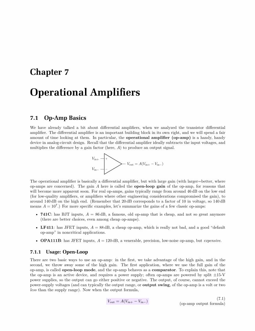
Chapter 7
Operational Amplifiers
7.1 Op-Amp Basics
We have already talked a bit about differential amplifiers, when we analyzed the transistor differentialamplifier. The differential amplifier is an important building block in its own right, and we will spend a fairamount of time looking at them. In particular, the operational amplifier (op-amp) is a handy, handydevice in analog-circuit design. Recall that the differential amplifier ideally subtracts the input voltages, andmultiplies the difference by a gain factor (here, A) to produce an output signal.
−
+
Vout = A(Vin+ − Vin−)
Vin+
Vin−
The operational amplifier is basically a differential amplifier, but with large gain (with larger=better, whereop-amps are concerned). The gain A here is called the open-loop gain of the op-amp, for reasons thatwill become more apparent soon. For real op-amps, gains typically range from around 46 dB on the low end(for low-quality amplifiers, or amplifiers where other engineering considerations compromised the gain), toaround 140 dB on the high end. (Remember that 20 dB corresponds to a factor of 10 in voltage, so 140 dBmeans A = 107.) For more specific examples, let’s summarize the gains of a few classic op-amps:
• 741C: has BJT inputs, A = 86 dB, a famous, old op-amp that is cheap, and not so great anymore(there are better choices, even among cheap op-amps).
• LF411: has JFET inputs, A = 88 dB, a cheap op-amp, which is really not bad, and a good “defaultop-amp” in noncritical applications.
• OPA111B: has JFET inputs, A = 120 dB, a venerable, precision, low-noise op-amp, but expensive.
7.1.1 Usage: Open-Loop
There are two basic ways to use an op-amp: in the first, we take advantage of the high gain, and in thesecond, we throw away some of the high gain. The first application, where we use the full gain of theop-amp, is called open-loop mode, and the op-amp behaves as a comparator. To explain this, note thatthe op-amp is an active device, and requires a power supply; often op-amps are powered by split ±15-Vpower supplies, so the output can go either positive or negative. The output, of course, cannot exceed thepower-supply voltages (and can typically the output range, or output swing, of the op-amp is a volt or twoless than the supply range). Now when the output formula,
Vout = A(Vin+ − Vin−)(7.1)
(op-amp output formula)
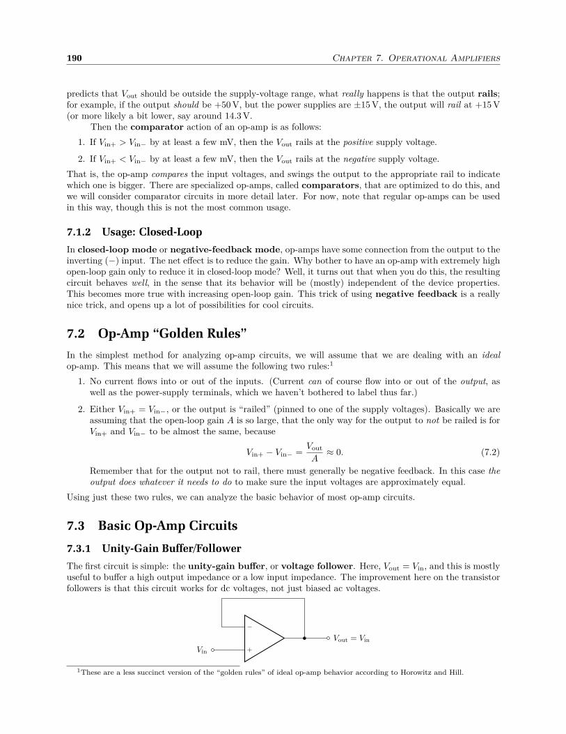
190 Chapter 7. Operational Amplifiers
predicts that Vout should be outside the supply-voltage range, what really happens is that the output rails;for example, if the output should be +50 V, but the power supplies are ±15 V, the output will rail at +15 V(or more likely a bit lower, say around 14.3 V.
Then the comparator action of an op-amp is as follows:
1. If Vin+ > Vin− by at least a few mV, then the Vout rails at the positive supply voltage.
2. If Vin+ < Vin− by at least a few mV, then the Vout rails at the negative supply voltage.
That is, the op-amp compares the input voltages, and swings the output to the appropriate rail to indicatewhich one is bigger. There are specialized op-amps, called comparators, that are optimized to do this, andwe will consider comparator circuits in more detail later. For now, note that regular op-amps can be usedin this way, though this is not the most common usage.
7.1.2 Usage: Closed-Loop
In closed-loop mode or negative-feedback mode, op-amps have some connection from the output to theinverting (−) input. The net effect is to reduce the gain. Why bother to have an op-amp with extremely highopen-loop gain only to reduce it in closed-loop mode? Well, it turns out that when you do this, the resultingcircuit behaves well, in the sense that its behavior will be (mostly) independent of the device properties.This becomes more true with increasing open-loop gain. This trick of using negative feedback is a reallynice trick, and opens up a lot of possibilities for cool circuits.
7.2 Op-Amp “Golden Rules”
In the simplest method for analyzing op-amp circuits, we will assume that we are dealing with an ideal
op-amp. This means that we will assume the following two rules:1
1. No current flows into or out of the inputs. (Current can of course flow into or out of the output, aswell as the power-supply terminals, which we haven’t bothered to label thus far.)
2. Either Vin+ = Vin−, or the output is “railed” (pinned to one of the supply voltages). Basically we areassuming that the open-loop gain A is so large, that the only way for the output to not be railed is forVin+ and Vin− to be almost the same, because
Vin+ − Vin− =Vout
A≈ 0. (7.2)
Remember that for the output not to rail, there must generally be negative feedback. In this case the
output does whatever it needs to do to make sure the input voltages are approximately equal.
Using just these two rules, we can analyze the basic behavior of most op-amp circuits.
7.3 Basic Op-Amp Circuits
7.3.1 Unity-Gain Buffer/Follower
The first circuit is simple: the unity-gain buffer, or voltage follower. Here, Vout = Vin, and this is mostlyuseful to buffer a high output impedance or a low input impedance. The improvement here on the transistorfollowers is that this circuit works for dc voltages, not just biased ac voltages.
−
+
Vout = Vin
Vin
1These are a less succinct version of the “golden rules” of ideal op-amp behavior according to Horowitz and Hill.
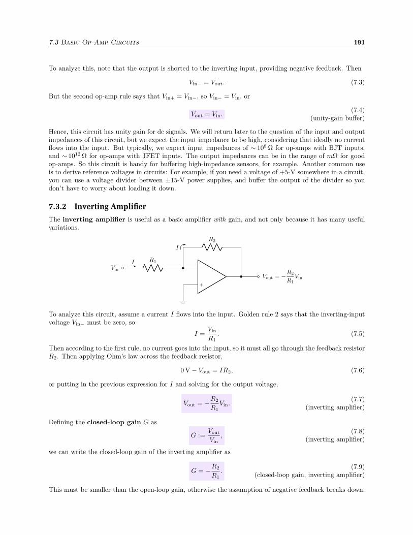
7.3 Basic Op-Amp Circuits 191
To analyze this, note that the output is shorted to the inverting input, providing negative feedback. Then
Vin− = Vout. (7.3)
But the second op-amp rule says that Vin+ = Vin−, so Vin− = Vin, or
Vout = Vin.(7.4)
(unity-gain buffer)
Hence, this circuit has unity gain for dc signals. We will return later to the question of the input and outputimpedances of this circuit, but we expect the input impedance to be high, considering that ideally no currentflows into the input. But typically, we expect input impedances of ∼ 108 Ω for op-amps with BJT inputs,and ∼ 1012 Ω for op-amps with JFET inputs. The output impedances can be in the range of mΩ for goodop-amps. So this circuit is handy for buffering high-impedance sensors, for example. Another common useis to derive reference voltages in circuits: For example, if you need a voltage of +5-V somewhere in a circuit,you can use a voltage divider between ±15-V power supplies, and buffer the output of the divider so youdon’t have to worry about loading it down.
7.3.2 Inverting Amplifier
The inverting amplifier is useful as a basic amplifier with gain, and not only because it has many usefulvariations.
I
I−
+
Vout = −R2
R1Vin
R2
R1
Vin
To analyze this circuit, assume a current I flows into the input. Golden rule 2 says that the inverting-inputvoltage Vin− must be zero, so
I =Vin
R1. (7.5)
Then according to the first rule, no current goes into the input, so it must all go through the feedback resistorR2. Then applying Ohm’s law across the feedback resistor,
0 V− Vout = IR2, (7.6)
or putting in the previous expression for I and solving for the output voltage,
Vout = −R2
R1Vin.
(7.7)(inverting amplifier)
Defining the closed-loop gain G as
G :=Vout
Vin,
(7.8)(inverting amplifier)
we can write the closed-loop gain of the inverting amplifier as
G = −R2
R1.
(7.9)(closed-loop gain, inverting amplifier)
This must be smaller than the open-loop gain, otherwise the assumption of negative feedback breaks down.

192 Chapter 7. Operational Amplifiers
7.3.2.1 Stability
Now it’s useful to try to get an idea of how feedback works in this circuit to maintain the advertised outputvoltage. An alternative to the above derivation is to think of R1 and R2 as forming a voltage divider withoutput Vin−; the voltage divider is unloaded because no current flows into the inverting input. Hence
Vin− = VinR2
R1 + R2+ Vout
R1
R1 + R2. (7.10)
Since the op-amp inputs must be equal, we can just set Vin− = 0, obtaining again the result (7.7). Butsuppose instead that the output has some small error ǫ, so that
Vout = −R2
R1Vin + ǫ. (7.11)
Putting this back into the voltage-divider result (7.10), the new voltage at the
Vin− =R1
R1 + R2ǫ, (7.12)
where notice that any contribution from Vin cancelled.For the op-amp to work properly, it should be stable: that is, the op-amp should tend to remove errors
like this. To see if this is the case, let’s substitute this new input voltage into the (finite-gain) output formula(7.1), which says Vout = A(Vin+ − Vin−):
∆Vout = − R1
R1 + R2A ǫ, (7.13)
We are notating this as a change in the output voltage, because this merely represents the tendency of theop-amp’s output. Since A is large, this is a strong tendency for the op-amp to move its output in oppositionto ǫ (so if ǫ is a small, positive error, the op-amp will feel a strong “desire” to reduce it’s voltage). Thus,any deviation away from ǫ = 0 makes the op-amp want to drive the output towards ǫ = 0, correcting theerror. So not only does the inverting amplifier satisfy the golden rules, but it is stable, in that the op-ampwill correct for deviations away from this value.
For now, though, this example allows us to be a little more precise about what we mean by “negativefeedback.” If we had instead build the inverting amplifier with the op-amp inputs swapped, the golden ruleswould still predict the same output voltage. However, the stability analysis would have led to the sameexpression (7.12), but for Vin+ instead of Vin−, and the op-amp’s desired change in Vout in Eq. (7.12) wouldhave had the opposite sign. This would mean that the op-amp would tend to strongly reinforce any smallerror, running away until the output rails.
One of the main powers of negative feedback is robustness to deviations (ǫ) from the proper output(e.g., due to power-supply noise). If the feedback is positive instead of negative (as in the “backwards”inverting amplifier), then more complicated behaviors like oscillation may result; we will return to this usefulcase later. In fact, even in the stability analysis above, it may seem that the zealous tendency of the op-ampto correct itself may lead to an overshooting output and thus an oscillation. In practice, if the op-amp’sresponse is quick enough, the circuit will move quickly to equilibrium (as the tendency of the op-amp toself-correct will disappear as ǫ −→ 0). However, a delayed between an output change and the input responsecan certainly lead to oscillation. Again, we will treat this later in terms of the varying frequency responseof the op-amp circuit.
One final note is in order here, because technically there is some sleight of hand in the above derivation.Since we are using the finite gain op-amp equation Vout = A(Vin+−Vin−) to analyze the stability, we shouldhave used the same relation to determine the output Vout in the first place. We will come back to this kind ofsolution later in Section 7.7, but for now it is sufficient to note that the result of redoing the correct analysisis that with the input error ǫ, we would have found that Vout is the expected solution plus the amplifiederror (see Problem 7.18 for an example). The “cheat” in the above derivation is in assuming that the outputsignal represented the change in output. However, this simple approach is usually sufficient to determinethe (dc) amplifier stability, provided we’re careful with the interpretation.
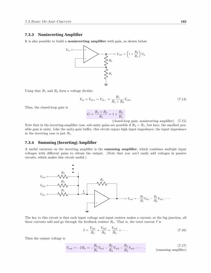
7.3 Basic Op-Amp Circuits 193
7.3.3 Noninverting Amplifier
It is also possible to build a noninverting amplifier with gain, as shown below.
−
+
Vout =
(
1 +R2
R1
)
Vin
R2
R1
Vin
Using that R1 and R2 form a voltage divider,
Vin = Vin+ = Vin− =R1
R1 + R2Vout. (7.14)
Thus, the closed-loop gain is
G =R1 + R2
R1= 1 +
R2
R1.
(closed-loop gain, noninverting amplifier) (7.15)Note that in the inverting-amplifier case, sub-unity gains are possible if R2 < R1, but here, the smallest pos-sible gain is unity. Like the unity-gain buffer, this circuit enjoys high input impedance; the input impedancein the inverting case is just R1.
7.3.4 Summing (Inverting) Amplifier
A useful variation on the inverting amplifier is the summing amplifier, which combines multiple inputvoltages with different gains to obtain the output. (Note that you can’t easily add voltages in passivecircuits, which makes this circuit useful.)
I−
+
Vout = −RF
R1Vin1 −
RF
R2Vin2 − · · ·
RF
R1
Vin1
R2
Vin2
R3
Vin3
The key to this circuit is that each input voltage and input resistor makes a current; at the big junction, allthese currents add and go through the feedback resistor RF. That is, the total current I is
I =Vin1
R1+
Vin2
R2+
Vin3
R3+ · · · . (7.16)
Then the output voltage is
Vout = −IRF = −RF
R1Vin1 −
RF
R2Vin2 −
RF
R3Vin3 − · · · .
(7.17)(summing amplifier)
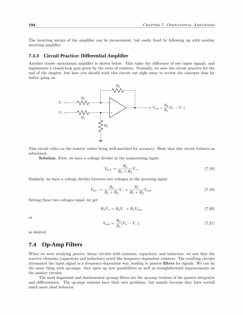
194 Chapter 7. Operational Amplifiers
The inverting nature of the amplifier can be inconvenient, but easily fixed by following up with anotherinverting amplifier.
7.3.5 Circuit Practice: Differential Amplifier
Another classic operational amplifier is shown below. This takes the difference of two input signals, andimplements a closed-loop gain given by the ratio of resistors. Normally, we save the circuit practice for theend of the chapter, but here you should work this circuit out right away to review the concepts thus farbefore going on.
−
+
Vout =R2
R1(V+ − V−)
R2
R1
V−
R1
V+
R2
This circuit relies on the resistor values being well-matched for accuracy. Show that this circuit behaves asadvertised.
Solution. First, we have a voltage divider at the noninverting input:
Vin+ =R2
R1 + R2V+. (7.18)
Similarly, we have a voltage divider between two voltages at the inverting input:
Vin− =R2
R1 + R2V− +
R1
R1 + R2Vout. (7.19)
Setting these two voltages equal, we get
R2V+ = R2V− + R1Vout, (7.20)
or
Vout =R2
R1(V+ − V−), (7.21)
as desired.
7.4 Op-Amp Filters
When we were studying passive, linear circuits with resistors, capacitors, and inductors, we saw that thereactive elements (capacitors and inductors) acted like frequency-dependent resistors. The resulting circuitsattenuated the input signal in a frequency-dependent way, leading to passive filters for signals. We can dothe same thing with op-amps: they open up new possibilities as well as straightforward improvements onthe passive circuits.
The most important and fundamental op-amp filters are the op-amp versions of the passive integratorand differentiator. The op-amp versions have their own problems, but mainly because they have overallmuch more ideal behavior.
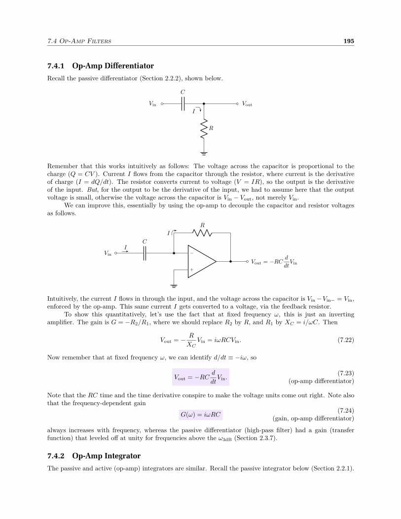
7.4 Op-Amp Filters 195
7.4.1 Op-Amp Differentiator
Recall the passive differentiator (Section 2.2.2), shown below.
I
Vin
C
R
Vout
Remember that this works intuitively as follows: The voltage across the capacitor is proportional to thecharge (Q = CV ). Current I flows from the capacitor through the resistor, where current is the derivativeof charge (I = dQ/dt). The resistor converts current to voltage (V = IR), so the output is the derivativeof the input. But, for the output to be the derivative of the input, we had to assume here that the outputvoltage is small, otherwise the voltage across the capacitor is Vin − Vout, not merely Vin.
We can improve this, essentially by using the op-amp to decouple the capacitor and resistor voltagesas follows.
I
I−
+
Vout = −RCd
dtVin
R
C
Vin
Intuitively, the current I flows in through the input, and the voltage across the capacitor is Vin−Vin− = Vin,enforced by the op-amp. This same current I gets converted to a voltage, via the feedback resistor.
To show this quantitatively, let’s use the fact that at fixed frequency ω, this is just an invertingamplifier. The gain is G = −R2/R1, where we should replace R2 by R, and R1 by XC = i/ωC. Then
Vout = − R
XCVin = iωRCVin. (7.22)
Now remember that at fixed frequency ω, we can identify d/dt ≡ −iω, so
Vout = −RCd
dtVin.
(7.23)(op-amp differentiator)
Note that the RC time and the time derivative conspire to make the voltage units come out right. Note alsothat the frequency-dependent gain
G(ω) = iωRC(7.24)
(gain, op-amp differentiator)
always increases with frequency, whereas the passive differentiator (high-pass filter) had a gain (transferfunction) that leveled off at unity for frequencies above the ω3dB (Section 2.3.7).
7.4.2 Op-Amp Integrator
The passive and active (op-amp) integrators are similar. Recall the passive integrator below (Section 2.2.1).
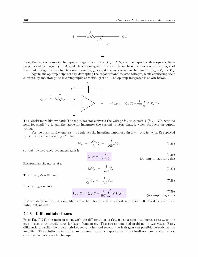
196 Chapter 7. Operational Amplifiers
I
Vin
R
C
Vout
Here, the resistor converts the input voltage to a current (Vin = IR), and the capacitor develops a voltageproportional to charge (Q = CV ), which is the integral of current. Hence the output voltage is the integral ofthe input voltage. But we had to assume small Vout, so that the voltage across the resistor is Vin−Vout ≈ Vin.
Again, the op-amp helps here by decoupling the capacitor and resistor voltages, while connecting theircurrents, by maintaing the inverting input at virtual ground. The op-amp integrator is shown below.
I
I−
+
Vout(t) = Vout(0)− 1
RC
∫ t
0
dt′ Vin(t′)
C
R
Vin
This works more like we said: The input resistor converts the voltage Vin to current I (Vin = IR, with noneed for small Vout), and the capacitor integrates the current to store charge, which produces an outputvoltage.
For the quantitative analysis, we again use the inverting-amplifier gain G = −R2/R1, with R2 replacedby XC , and R1 replaced by R. Then
Vout = −XC
RVin = − i
ωRCVin, (7.25)
so that the frequency-dependent gain is
G(ω) = − i
ωRC.
(7.26)(op-amp integrator gain)
Rearranging the factor of ω,
− iωVout = − 1
RCVin. (7.27)
Then using d/dt ≡ −iω,d
dtVout = − 1
RCVin. (7.28)
Integrating, we have
Vout(t) = Vout(0)− 1
RC
∫ t
0
dt′ Vin(t′).(7.29)
(op-amp integrator)
Like the differentiator, this amplifier gives the integral with an overall minus sign. It also depends on theinitial output state.
7.4.3 Differentiator Issues
From Eq. (7.24), the main problem with the differentiator is that it has a gain that increases as ω, so thegain becomes arbitrarily large for large frequencies. This causes potential problems in two ways. First,differentiators suffer from bad high-frequency noise, and second, the high gain can possibly de-stabilize theamplifier. The solution is to add an extra, small, parallel capacitance in the feedback look, and an extra,small, series resistance in the input.
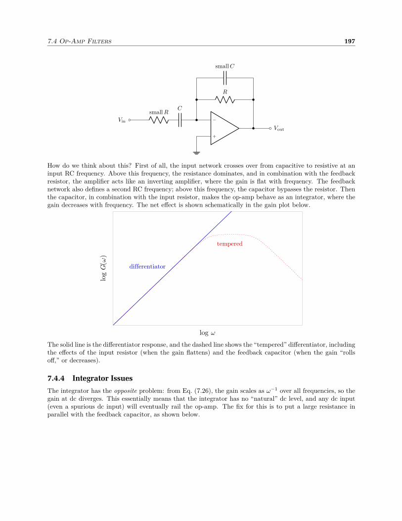
7.4 Op-Amp Filters 197
−
+
Vout
R
small C
Csmall R
Vin
How do we think about this? First of all, the input network crosses over from capacitive to resistive at aninput RC frequency. Above this frequency, the resistance dominates, and in combination with the feedbackresistor, the amplifier acts like an inverting amplifier, where the gain is flat with frequency. The feedbacknetwork also defines a second RC frequency; above this frequency, the capacitor bypasses the resistor. Thenthe capacitor, in combination with the input resistor, makes the op-amp behave as an integrator, where thegain decreases with frequency. The net effect is shown schematically in the gain plot below.
log w
log G
(w)
differentiator
tempered
The solid line is the differentiator response, and the dashed line shows the “tempered” differentiator, includingthe effects of the input resistor (when the gain flattens) and the feedback capacitor (when the gain “rollsoff,” or decreases).
7.4.4 Integrator Issues
The integrator has the opposite problem: from Eq. (7.26), the gain scales as ω−1 over all frequencies, so thegain at dc diverges. This essentially means that the integrator has no “natural” dc level, and any dc input(even a spurious dc input) will eventually rail the op-amp. The fix for this is to put a large resistance inparallel with the feedback capacitor, as shown below.

198 Chapter 7. Operational Amplifiers
−
+
Vout
C
large R
R
Vin
The feedback network then defines an RC frequency (a small frequency, since the resistance is large), belowwhich the resistor dominates the feedback impedance, and the op-amp acts as an inverting amplifier. Thislevels the low-frequency gain to some finite value, as illustrated schematically below.
log w
log G
(w)
differentiator
tempered
This shows the normal −6-dB scaling of the integrator as the solid line, with the dashed line showing the“tempered” behavior with the feedback resistor rolling off the low-frequency gain.
7.4.5 Sources of Integrator Error
We have mentioned that the basic integrator is very sensitive to spurious dc inputs, due to the divergent dcgain. What are these spurious dc offsets? There are two main sources for op-amps: input bias current, andinput offset voltage.
7.4.5.1 Input Bias Current
In the ideal op-amp we stated the golden rule that no current flows into the inputs. However, this isn’t quite
true. The idea behind the input bias current is that in fact a small current flows into (or out of) the inputs,which makes sense, as the op-amp inputs drive internal transistors, which either require current to work orallow a bit of leakage current to flow. For BJT-input op-amps, the input bias current is ∼10 nA, while forJFET-input op-amps, the input bias current is ∼ 10 pA. For example, the precision OPA602C with JFETinputs has a 1-pA input bias current (compared to the 741C with BJT inputs at 500 nA). Thus, JFET-inputop-amps are the clear winner in this regard. To some extent, it is possible to compensate for the input biascurrent by injecting a small, adjustable current at the inverting input.
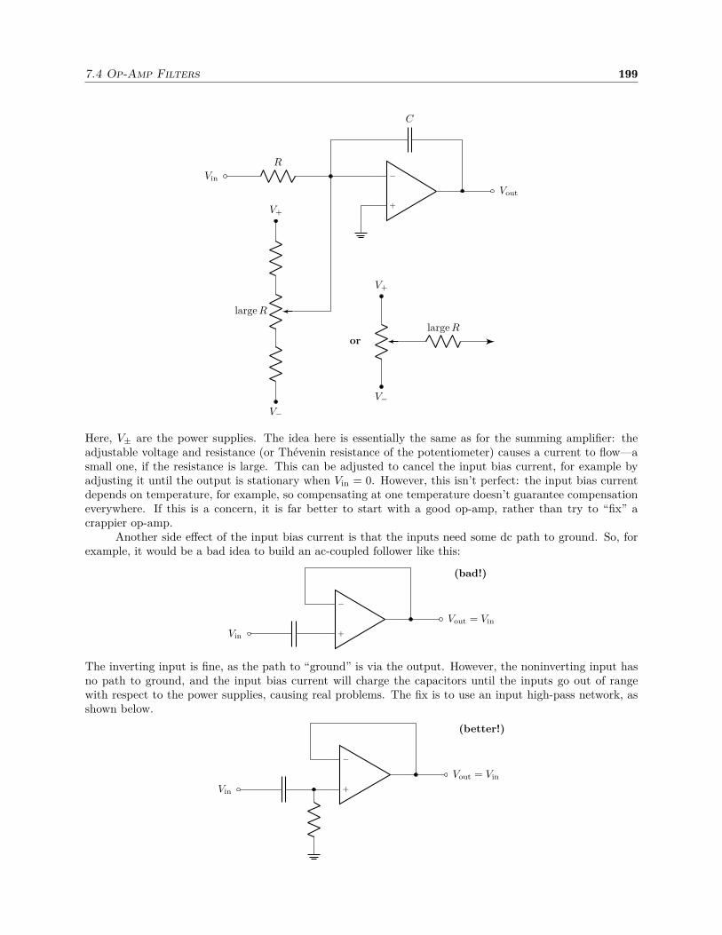
7.4 Op-Amp Filters 199
−
+
Vout
C
R
Vin
large R
V−
V+
or
V−
V+
large R
Here, V± are the power supplies. The idea here is essentially the same as for the summing amplifier: theadjustable voltage and resistance (or Thévenin resistance of the potentiometer) causes a current to flow—asmall one, if the resistance is large. This can be adjusted to cancel the input bias current, for example byadjusting it until the output is stationary when Vin = 0. However, this isn’t perfect: the input bias currentdepends on temperature, for example, so compensating at one temperature doesn’t guarantee compensationeverywhere. If this is a concern, it is far better to start with a good op-amp, rather than try to “fix” acrappier op-amp.
Another side effect of the input bias current is that the inputs need some dc path to ground. So, forexample, it would be a bad idea to build an ac-coupled follower like this:
(bad!)
−
+
Vout = Vin
Vin
The inverting input is fine, as the path to “ground” is via the output. However, the noninverting input hasno path to ground, and the input bias current will charge the capacitors until the inputs go out of rangewith respect to the power supplies, causing real problems. The fix is to use an input high-pass network, asshown below.
(better!)
−
+
Vout = Vin
Vin
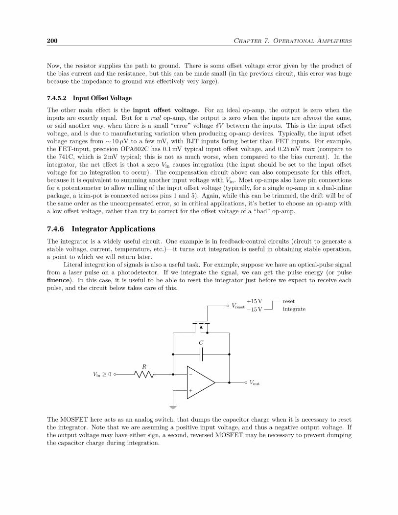
200 Chapter 7. Operational Amplifiers
Now, the resistor supplies the path to ground. There is some offset voltage error given by the product ofthe bias current and the resistance, but this can be made small (in the previous circuit, this error was hugebecause the impedance to ground was effectively very large).
7.4.5.2 Input Offset Voltage
The other main effect is the input offset voltage. For an ideal op-amp, the output is zero when theinputs are exactly equal. But for a real op-amp, the output is zero when the inputs are almost the same,or said another way, when there is a small “error” voltage δV between the inputs. This is the input offsetvoltage, and is due to manufacturing variation when producing op-amp devices. Typically, the input offsetvoltage ranges from ∼ 10 µV to a few mV, with BJT inputs faring better than FET inputs. For example,the FET-input, precision OPA602C has 0.1 mV typical input offset voltage, and 0.25 mV max (compare tothe 741C, which is 2 mV typical; this is not as much worse, when compared to the bias current). In theintegrator, the net effect is that a zero Vin causes integration (the input should be set to the input offsetvoltage for no integration to occur). The compensation circuit above can also compensate for this effect,because it is equivalent to summing another input voltage with Vin. Most op-amps also have pin connectionsfor a potentiometer to allow nulling of the input offset voltage (typically, for a single op-amp in a dual-inlinepackage, a trim-pot is connected across pins 1 and 5). Again, while this can be trimmed, the drift will be ofthe same order as the uncompensated error, so in critical applications, it’s better to choose an op-amp witha low offset voltage, rather than try to correct for the offset voltage of a “bad” op-amp.
7.4.6 Integrator Applications
The integrator is a widely useful circuit. One example is in feedback-control circuits (circuit to generate astable voltage, current, temperature, etc.)—it turns out integration is useful in obtaining stable operation,a point to which we will return later.
Literal integration of signals is also a useful task. For example, suppose we have an optical-pulse signalfrom a laser pulse on a photodetector. If we integrate the signal, we can get the pulse energy (or pulsefluence). In this case, it is useful to be able to reset the integrator just before we expect to receive eachpulse, and the circuit below takes care of this.
−
+
Vout
C
Vreset
R
Vin ≥ 0
integrate
reset
−15 V
+15 V
The MOSFET here acts as an analog switch, that dumps the capacitor charge when it is necessary to resetthe integrator. Note that we are assuming a positive input voltage, and thus a negative output voltage. Ifthe output voltage may have either sign, a second, reversed MOSFET may be necessary to prevent dumpingthe capacitor charge during integration.

7.5 Instrumentation Amplifiers 201
7.5 Instrumentation Amplifiers
Recall the op-amp differential amplifier, shown below, from Section 7.3.5.
−
+
Vout =R2
R1(V+ − V−)
R2
R1
V−
R1
V+
R2
This circuit works fine, but has some disadvantages:
• This circuit does not have high input impedances, especially for large gains. Specifically, you shouldconvince yourself that the noninverting input has an input impedance R1 + R2, while the invertinginput has an input impedance R1. But, for example, if R1 = 1 kΩ and R2 = 10 kΩ, so that G = 10,the input impedance is at worst 1 kΩ.
• The circuit requires accurately matched resistor pairs to achieve a high CMRR. To obtain a CMRRof 80 dB, the resistors must have a tolerance of around 0.01% at G = 1; resistors this accurate aretypically wirewound, but these don’t work well at high frequencies.
• Any source impedances add to the input R1’s. That is, the sources must act as ideal voltage sources,otherwise the gain and CMRR may be affected. For example, if R1 = 1 kΩ, the source impedance mustbe 10 Ω or less for 1% gain accuracy. Even worse, the source impedances must be matched to ensuregood CMRR.
The main solution to these problems, especially that of source impedances interacting with the resistancesin the op-amp circuit, is to simply buffer the inputs. A differential amplifier with buffered (high-impedance)inputs is called an instrumentation amplifier, and the basic circuit is shown below.
−
+
Vout =R2
R1(V+ − V−)
R2
R2
−
+
−
+
R1
R1
V−
V+
The point is that this entire circuit should come in a single package, with laser-trimmed (matched) resistornetworks, for good performance and to make life easy. This also guarantees that any errors in the matchedresistor pairs due to temperature drifts is kept to a minimum.
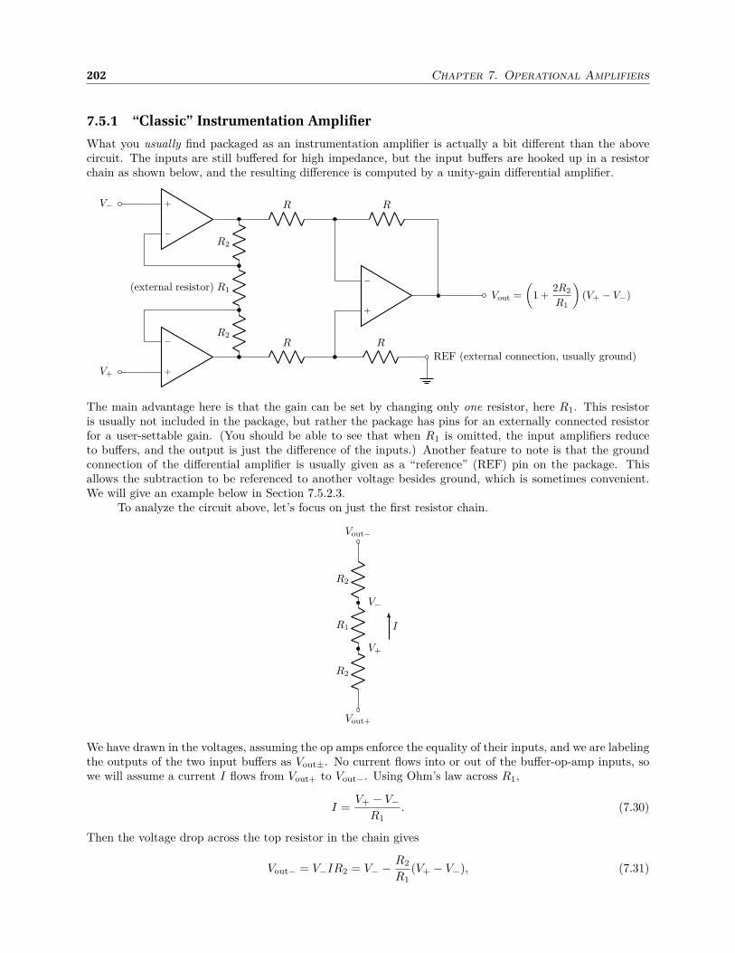
202 Chapter 7. Operational Amplifiers
7.5.1 “Classic” Instrumentation Amplifier
What you usually find packaged as an instrumentation amplifier is actually a bit different than the abovecircuit. The inputs are still buffered for high impedance, but the input buffers are hooked up in a resistorchain as shown below, and the resulting difference is computed by a unity-gain differential amplifier.
−
+
Vout =
(
1 +2R2
R1
)
(V+ − V−)
R
R
REF (external connection, usually ground)
−
+
−
+R
R
V−
V+
R2
(external resistor) R1
R2
The main advantage here is that the gain can be set by changing only one resistor, here R1. This resistoris usually not included in the package, but rather the package has pins for an externally connected resistorfor a user-settable gain. (You should be able to see that when R1 is omitted, the input amplifiers reduceto buffers, and the output is just the difference of the inputs.) Another feature to note is that the groundconnection of the differential amplifier is usually given as a “reference” (REF) pin on the package. Thisallows the subtraction to be referenced to another voltage besides ground, which is sometimes convenient.We will give an example below in Section 7.5.2.3.
To analyze the circuit above, let’s focus on just the first resistor chain.
Vout+
R2
R1
R2
Vout−
V+
V−
I
We have drawn in the voltages, assuming the op amps enforce the equality of their inputs, and we are labelingthe outputs of the two input buffers as Vout±. No current flows into or out of the buffer-op-amp inputs, sowe will assume a current I flows from Vout+ to Vout−. Using Ohm’s law across R1,
I =V+ − V−
R1. (7.30)
Then the voltage drop across the top resistor in the chain gives
Vout− = V−IR2 = V− −R2
R1(V+ − V−), (7.31)

7.5 Instrumentation Amplifiers 203
and across the bottom resistor in the chain,
Vout+ = V + +IR2 = V+ +R2
R1(V+ − V−). (7.32)
Now the differential amplifier takes the difference between Vout+ and Vout−, so
Vout = Vout+ − Vout− = (V+ − V−) +2R2
R1(V+ − V−), (7.33)
or
Vout =
(
1 +2R2
R1
)
(V+ − V−).(7.34)
(instrumentation-amplifier output)
As a gain, this reads
G =
(
1 +2R2
R1
)
.(7.35)
(instrumentation-amplifier gain)
Thus we see again if R1 is omitted (R1 =∞), the gain is unity, while other values can serve to increase thegain above unity.
A good example of an instrumentation amplifier is the INA128 from Burr-Brown, one of a family of“INAXXX” instrumentation amplifiers. In the INA128, the internal R2 resistors are 50 kΩ, so the externalresistor RG (i.e., R1), sets the gain via
G = 1 +50 kΩ
RG
. (7.36)
The CMRR is 86 dB at unity gain (RG = ∞), and 125 dB at G = 100. The input impedance is ∼ 1010 Ω,and the input bias current is 2 nA. These cost ∼$8 each, depending on the grade (quality) and package.
7.5.2 Instrumentation-Amplifier Applications
7.5.2.1 Thermocouple Amplifier
The instrumentation amplifier turns out to be really useful in a number of applications, particularly inamplifying high-source-impedance sensors that require high gain. On example, shown below, is a simplisticthermocouple amplifier.
−
+
INA128
REF
RG (set for G = 100)
Voutthermocouple junction
10 kΩ
A thermocouple is a junction of two dissimilar metals that develops a voltage that is related (in annonlinear way) to the temperature. Typical signal levels from thermocouples range from ∼10 µV to 100 µV,so significant gain is useful here. Note that this circuit is simplistic in the sense that it is only usefulfor measuring relative temperature changes. Absolute calibration requires more information, because thethermocouple wires must make a transition to copper on the way to the amplifier, and these copper junctions(and their temperature) contribute to the output voltage. The underlying physical mechanism is the Seebeckeffect: a temperature gradient over the length of a wire (of a single material) causes charges to migratecreating a potential difference from one end to the other. The voltage is material dependent, so using twodifferent wires in the thermocouple junction gives information about the temperature difference between the
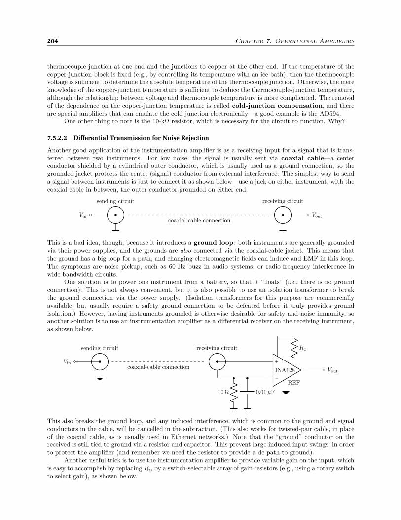
204 Chapter 7. Operational Amplifiers
thermocouple junction at one end and the junctions to copper at the other end. If the temperature of thecopper-junction block is fixed (e.g., by controlling its temperature with an ice bath), then the thermocouplevoltage is sufficient to determine the absolute temperature of the thermocouple junction. Otherwise, the mereknowledge of the copper-junction temperature is sufficient to deduce the thermocouple-junction temperature,although the relationship between voltage and thermocouple temperature is more complicated. The removalof the dependence on the copper-junction temperature is called cold-junction compensation, and thereare special amplifiers that can emulate the cold junction electronically—a good example is the AD594.
One other thing to note is the 10-kΩ resistor, which is necessary for the circuit to function. Why?
7.5.2.2 Differential Transmission for Noise Rejection
Another good application of the instrumentation amplifier is as a receiving input for a signal that is trans-ferred between two instruments. For low noise, the signal is usually sent via coaxial cable—a centerconductor shielded by a cylindrical outer conductor, which is usually used as a ground connection, so thegrounded jacket protects the center (signal) conductor from external interference. The simplest way to senda signal between instruments is just to connect it as shown below—use a jack on either instrument, with thecoaxial cable in between, the outer conductor grounded on either end.
Voutcoaxial-cable connection
Vin
sending circuit receiving circuit
This is a bad idea, though, because it introduces a ground loop: both instruments are generally groundedvia their power supplies, and the grounds are also connected via the coaxial-cable jacket. This means thatthe ground has a big loop for a path, and changing electromagnetic fields can induce and EMF in this loop.The symptoms are noise pickup, such as 60-Hz buzz in audio systems, or radio-frequency interference inwide-bandwidth circuits.
One solution is to power one instrument from a battery, so that it “floats” (i.e., there is no groundconnection). This is not always convenient, but it is also possible to use an isolation transformer to breakthe ground connection via the power supply. (Isolation transformers for this purpose are commerciallyavailable, but usually require a safety ground connection to be defeated before it truly provides groundisolation.) However, having instruments grounded is otherwise desirable for safety and noise immunity, soanother solution is to use an instrumentation amplifier as a differential receiver on the receiving instrument,as shown below.
−
+
INA128
REF
RG
Vout
0.01 µF10 Ω
coaxial-cable connectionVin
sending circuit receiving circuit
This also breaks the ground loop, and any induced interference, which is common to the ground and signalconductors in the cable, will be cancelled in the subtraction. (This also works for twisted-pair cable, in placeof the coaxial cable, as is usually used in Ethernet networks.) Note that the “ground” conductor on thereceived is still tied to ground via a resistor and capacitor. This prevent large induced input swings, in orderto protect the amplifier (and remember we need the resistor to provide a dc path to ground).
Another useful trick is to use the instrumentation amplifier to provide variable gain on the input, whichis easy to accomplish by replacing RG by a switch-selectable array of gain resistors (e.g., using a rotary switchto select gain), as shown below.

7.5 Instrumentation Amplifiers 205
∞Ω (G = 1)
49.9 kΩ (G = 2)
12.1 kΩ (G = 5)
4.99 kΩ (G = 10)
RG
A logarithmic spacing of gains (1, 2, 5, 10, 20, 50, 100, . . . ) covers a wide gain range in a useful way.
7.5.2.3 AC-Coupled Inputs with High Impedance
Sometimes it is useful to have an ac-coupled input, but with high input impedance. For example, we mayhave a sensor with a weak signal and high source impedance that requires large amplification, but if it hasa large dc bias, a large gain would take the dc bias out of range. If we just use a capacitor to block dc onthe input, this is bad, remember, because we need a dc path to ground on each input.
−
+
An improvement is to introduce a resistor, which makes a high-pass filter. The resistor prevents problemsfrom input bias currents.
−
+
R
However, in the pass band, the input impedance is limited to R, which will not be nearly as good as a“bare” input on a decent op-amp. A clever solution is to use an integrator to feed back the output of aninstrumentation amplifier to the reference input.
−
+
−
+
INA128
REF
Vout
CR
Assume for simplicity that the instrumentation amplifier is set for unity gain, so
Vout = V+ − V− + VREF. (7.37)
That is, the reference voltage is the reference for ground, so the amplifier sets Vout − VREF to the differenceV+ − V−. Note that the only steady state occurs when the integrator is at steady state, which is when theintegrator input (Vout) is zero. If Vout 6= 0, the integrator will build up a voltage until it cancels the steadyoutput voltage on a time scale RC (with negative feedback due to the inverting nature of the integrator).

206 Chapter 7. Operational Amplifiers
High-frequency signals are not affected by the integrator, because the integrator has no time to “catch up”to the rapidly changing output (which is saying that the integrator gain is suppressed at high frequencies as1/ω). To make this input switchable between ac and dc, a switch can short across the capacitor to changethe instrumentation amplifier to dc mode.
7.6 Practical Considerations
In this section, we will deal some more with some deviations of op-amps from their ideal behavior, and afew common tricks to mitigate these effects.
7.6.1 Input-Bias Currents and Precision Amplifiers
Before, when we were dealing with integrating amplifiers (Section 7.4.4), we talked about input-bias currentsand how they can cause problems by charging up the integrating capacitor, even with a zero input voltage.We also talked about how it is critical to have a dc path to ground for each input to prevent similar chargingproblems. However, input bias currents can still cause problems (albeit usually less serious) in “regular”op-amp circuits like inverting and noninverting amplifiers.
7.6.1.1 Inverting Amplifier
For example, let’s return to the inverting amplifier (Section 7.3.2).
−
+
Vout = −R2
R1Vin
R2
R1
Vin
As a numerical example, consider a 741C (a lower-grade op-amp that will make such problems obvious),with a worst-case input bias current of 0.5 µA. If we take R1 = 10 kΩ and R2 = 1 MΩ (for G = −100), thenthe inverting input sees a Thévenin-equivalent input resistance of RTh = R1‖R2 ≈ 10 kΩ. The input biascurrent then leads to a bias voltage of (0.5 µA)(10 kΩ) = 5 mV at the input. With a gain of (−100), thisleads to an output bias voltage of 5 V worst-case, which is pretty bad! (That is, for Vin = 0, it is permissibleaccording to the 741C’s specs to have |Vout| as much as 5 V.)
How do we get around this? There are a few approaches:
• Since this is a dc-bias issue, this is no problem for ac circuits—just make sure to design for zero dcgain in the circuit (using a blocking capacitor, for instance).
• The main problem in the example was an underwhelming performer of an op-amp (by modern stan-dards, anyway). Of course, we can do better, and recall that FET-input op-amps are superior toBJT-input op-amps in terms of bias currents. Precision BJT-input op-amps are a good option, too.For example, the FET-input LF411 has Ibias ≈ 0.2 nA, so the output error is only 0.2 mV in the aboveexample.
• For BJT-input op-amps, or in high-precision circuits, we can also reduce errors by balancing inputimpedances, which is best illustrated by a few examples.

7.6 Practical Considerations 207
7.6.1.2 Balanced Input-Impedances: Inverting Amplifier
To balance the input impedances of the inverting amplifier, recall that the problem came from the invertinginput “seeing” an effective source impedance of R1‖R2. We can simply insert an equivalent source impedanceon the noninverting input as shown below.
−
+
Vout = −R2
R1Vin
R2
R1
Vin
R1‖R2
This resistor does nothing for an ideal op-amp, because no current flows through the resistor (and thus theresistor drops no voltage), but for a real op-amp, this trick reduces bias errors. Of course, all this assumesVin acts like an ideal voltage source (i.e., it has a source impedance much smaller than R1), otherwise thesource impedance of Vin must also enter into the compensation scheme.
7.6.1.3 Balanced Input-Impedances: Noninverting Amplifier
Similar balancing tricks are possible for noninverting amplifiers. Recall the basic noninverting amplifier(Section 7.3.3), shown below.
−
+
Vout =
(
1 +R2
R1
)
Vin
R2
R1
Vin
Here, the inverting input sees a source impedance of R1‖R2, due to the voltage divider. Thus, it is again asimple matter to insert an equivalent source impedance for the other input.
−
+
Vout =
(
1 +R2
R1
)
Vin
R2
R1
R1‖R2
Vin
Balancing input impedances is a bit trickier for ac-coupled amplifiers. A good example is shown below.
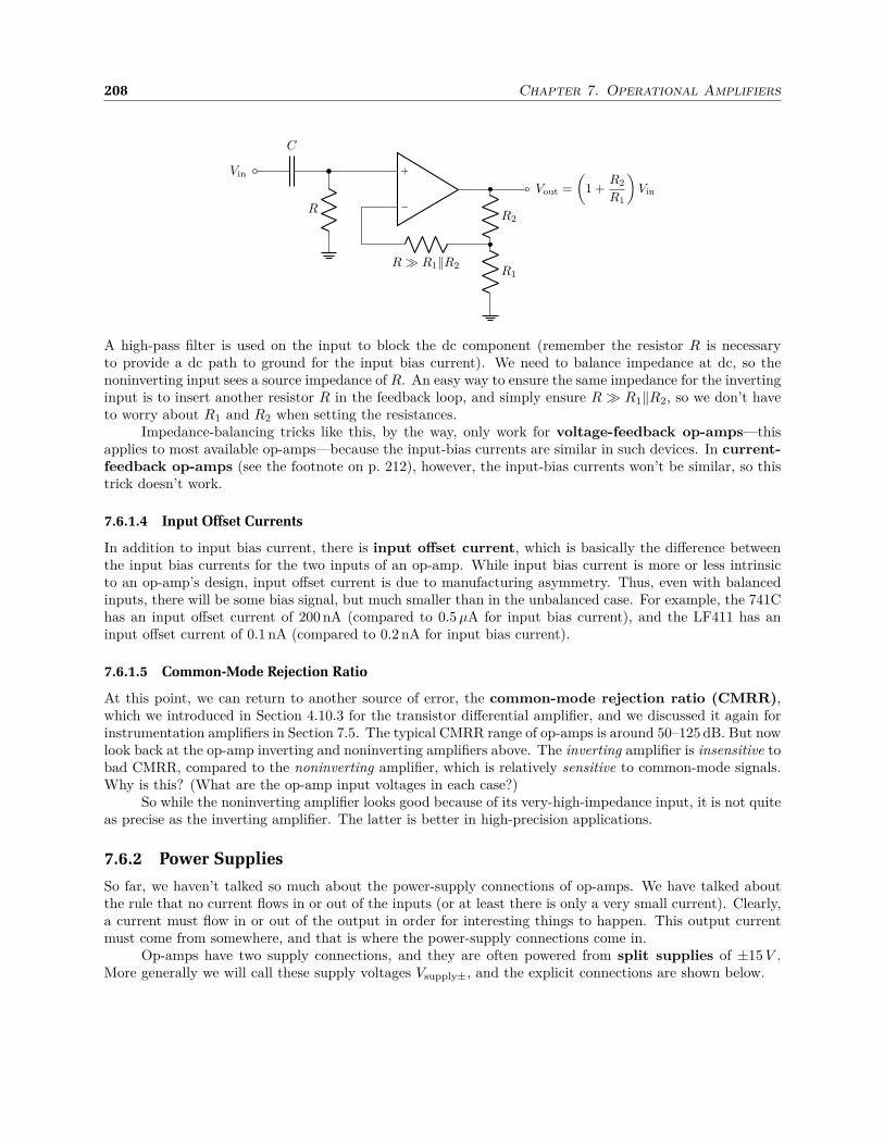
208 Chapter 7. Operational Amplifiers
−
+
Vout =
(
1 +R2
R1
)
Vin
R2
R1R≫ R1‖R2
C
Vin
R
A high-pass filter is used on the input to block the dc component (remember the resistor R is necessaryto provide a dc path to ground for the input bias current). We need to balance impedance at dc, so thenoninverting input sees a source impedance of R. An easy way to ensure the same impedance for the invertinginput is to insert another resistor R in the feedback loop, and simply ensure R≫ R1‖R2, so we don’t haveto worry about R1 and R2 when setting the resistances.
Impedance-balancing tricks like this, by the way, only work for voltage-feedback op-amps—thisapplies to most available op-amps—because the input-bias currents are similar in such devices. In current-feedback op-amps (see the footnote on p. 212), however, the input-bias currents won’t be similar, so thistrick doesn’t work.
7.6.1.4 Input Offset Currents
In addition to input bias current, there is input offset current, which is basically the difference betweenthe input bias currents for the two inputs of an op-amp. While input bias current is more or less intrinsicto an op-amp’s design, input offset current is due to manufacturing asymmetry. Thus, even with balancedinputs, there will be some bias signal, but much smaller than in the unbalanced case. For example, the 741Chas an input offset current of 200 nA (compared to 0.5 µA for input bias current), and the LF411 has aninput offset current of 0.1 nA (compared to 0.2 nA for input bias current).
7.6.1.5 Common-Mode Rejection Ratio
At this point, we can return to another source of error, the common-mode rejection ratio (CMRR),which we introduced in Section 4.10.3 for the transistor differential amplifier, and we discussed it again forinstrumentation amplifiers in Section 7.5. The typical CMRR range of op-amps is around 50–125 dB. But nowlook back at the op-amp inverting and noninverting amplifiers above. The inverting amplifier is insensitive tobad CMRR, compared to the noninverting amplifier, which is relatively sensitive to common-mode signals.Why is this? (What are the op-amp input voltages in each case?)
So while the noninverting amplifier looks good because of its very-high-impedance input, it is not quiteas precise as the inverting amplifier. The latter is better in high-precision applications.
7.6.2 Power Supplies
So far, we haven’t talked so much about the power-supply connections of op-amps. We have talked aboutthe rule that no current flows in or out of the inputs (or at least there is only a very small current). Clearly,a current must flow in or out of the output in order for interesting things to happen. This output currentmust come from somewhere, and that is where the power-supply connections come in.
Op-amps have two supply connections, and they are often powered from split supplies of ±15 V .More generally we will call these supply voltages Vsupply±, and the explicit connections are shown below.
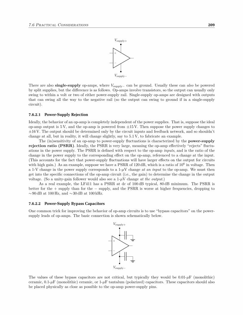
7.6 Practical Considerations 209
−
+
Vsupply−
Vsupply+
There are also single-supply op-amps, where Vsupply− can be ground. Usually these can also be poweredby split supplies, but the difference is as follows. Op-amps involve transistors, so the output can usually onlyswing to within a volt or two of either power-supply rail. Single-supply op-amps are designed with outputsthat can swing all the way to the negative rail (so the output can swing to ground if in a single-supplycircuit).
7.6.2.1 Power-Supply Rejection
Ideally, the behavior of an op-amp is completely independent of the power supplies. That is, suppose the idealop-amp output is 5 V, and the op-amp is powered from ±15 V. Then suppose the power supply changes to±16 V. The output should be determined only by the circuit inputs and feedback network, and so shouldn’tchange at all, but in reality, it will change slightly, say to 5.1 V, to fabricate an example.
The (in)sensitivity of an op-amp to power-supply fluctuations is characterized by the power-supplyrejection ratio (PSRR). Ideally, the PSRR is very large, meaning the op-amp effectively “rejects” fluctu-ations in the power supply. The PSRR is defined with respect to the op-amp inputs, and is the ratio of thechange in the power supply to the corresponding effect on the op-amp, referenced to a change at the input.(This accounts for the fact that power-supply fluctuations will have larger effects on the output for circuitswith high gain.) As an example, suppose we have a PSRR of 120 dB, which is a ratio of 106 in voltage. Thena 1-V change in the power supply corresponds to a 1-µV change at an input to the op-amp. We must thenget into the specific connections of the op-amp circuit (i.e., the gain) to determine the change in the outputvoltage. (So a unity-gain follower would also see a 1-µV change at the output.)
As a real example, the LF411 has a PSRR at dc of 100 dB typical, 80 dB minimum. The PSRR isbetter for the + supply than for the − supply, and the PSRR is worse at higher frequencies, dropping to∼90 dB at 100 Hz, and ∼30 dB at 100 kHz.
7.6.2.2 Power-Supply Bypass Capacitors
One common trick for improving the behavior of op-amp circuits is to use “bypass capacitors” on the power-supply leads of op-amps. The basic connection is shown schematically below.
−
+
Vsupply−
Vsupply+
The values of these bypass capacitors are not critical, but typically they would be 0.01-µF (monolithic)ceramic, 0.1-µF (monolithic) ceramic, or 1-µF tantalum (polarized) capacitors. These capacitors should alsobe placed physically as close as possible to the op-amp power-supply pins.
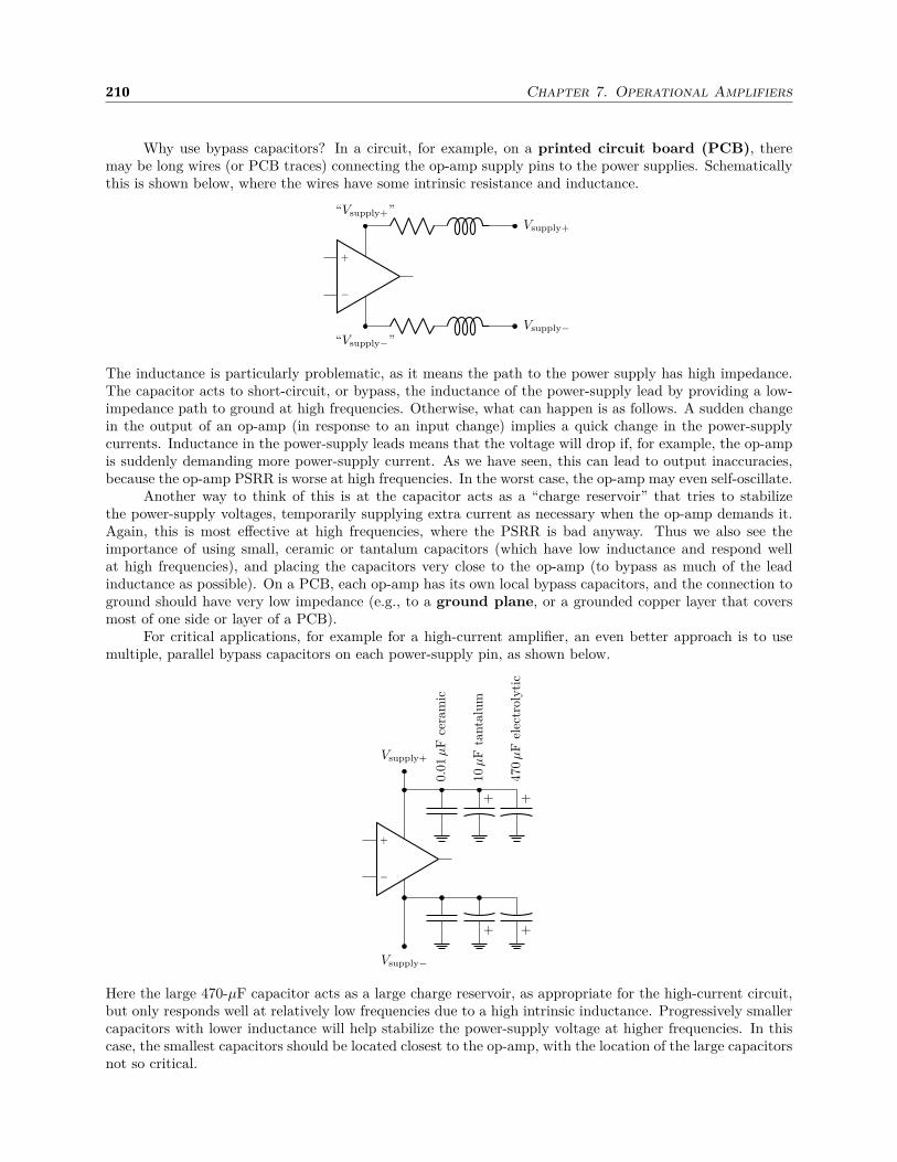
210 Chapter 7. Operational Amplifiers
Why use bypass capacitors? In a circuit, for example, on a printed circuit board (PCB), theremay be long wires (or PCB traces) connecting the op-amp supply pins to the power supplies. Schematicallythis is shown below, where the wires have some intrinsic resistance and inductance.
−
+
“Vsupply−”
“Vsupply+”
Vsupply−
Vsupply+
The inductance is particularly problematic, as it means the path to the power supply has high impedance.The capacitor acts to short-circuit, or bypass, the inductance of the power-supply lead by providing a low-impedance path to ground at high frequencies. Otherwise, what can happen is as follows. A sudden changein the output of an op-amp (in response to an input change) implies a quick change in the power-supplycurrents. Inductance in the power-supply leads means that the voltage will drop if, for example, the op-ampis suddenly demanding more power-supply current. As we have seen, this can lead to output inaccuracies,because the op-amp PSRR is worse at high frequencies. In the worst case, the op-amp may even self-oscillate.
Another way to think of this is at the capacitor acts as a “charge reservoir” that tries to stabilizethe power-supply voltages, temporarily supplying extra current as necessary when the op-amp demands it.Again, this is most effective at high frequencies, where the PSRR is bad anyway. Thus we also see theimportance of using small, ceramic or tantalum capacitors (which have low inductance and respond wellat high frequencies), and placing the capacitors very close to the op-amp (to bypass as much of the leadinductance as possible). On a PCB, each op-amp has its own local bypass capacitors, and the connection toground should have very low impedance (e.g., to a ground plane, or a grounded copper layer that coversmost of one side or layer of a PCB).
For critical applications, for example for a high-current amplifier, an even better approach is to usemultiple, parallel bypass capacitors on each power-supply pin, as shown below.
−
+
Vsupply−
++
Vsupply+
++
0.01
µF
cera
mic
10
µF
tanta
lum
470
µF
elec
trol
yti
c
Here the large 470-µF capacitor acts as a large charge reservoir, as appropriate for the high-current circuit,but only responds well at relatively low frequencies due to a high intrinsic inductance. Progressively smallercapacitors with lower inductance will help stabilize the power-supply voltage at higher frequencies. In thiscase, the smallest capacitors should be located closest to the op-amp, with the location of the large capacitorsnot so critical.

7.7 Finite-Gain Analysis 211
Another good approach for a low-current, or low-level, precision op-amp circuit is as shown below.
−
+
10 Ω
Vsupply−
10 Ω
Vsupply+
0.1 µF
0.1 µF
The idea is to add extra resistance to the power-supply lines, before the bypass capacitor. Obviously, thistrick is limited to low-current circuits, so the voltage drop due to the 10-Ω resistor is small. This resistorenhances the effect of the bypass capacitor and gives improved isolation from power-supply fluctuations.This is an especially useful technique if high- and low-current amplifiers coexist in the same circuit, wherefeedback from the high-current to low-current amplifiers may cause the circuit to self-oscillate. Even better isto make sure the high-current and low-current ICs do not share the same power-supply lines (they should useseparate lines, connected only at a point where the supply voltage is regulated, for example, by a 3-terminalregulator).
7.7 Finite-Gain Analysis
So far, we have assumed that the open-loop gain A of the op-amp is arbitrarily large. We have mainlymade this assumption via the rule that the input voltages are the same in negative-feedback mode. In areal op-amp, this open-loop gain is high, but finite, ranging from about ∼50–146 dB. So now let’s relax theassumption of infinite open-loop gain to (1) see what the effects are, and (2) to see why having a large gainis a good thing in an op-amp.
7.7.1 Noninverting Amplifier
As a first example, let’s return to the noninverting-amplifier circuit of Section 7.3.3, shown below.
−
+
Vout
R2
R1
Vin
212 Chapter 7. Operational Amplifiers
Recall that the result with infinite open-loop gain was
Vout =
(
1 +R2
R1
)
Vin. (7.38)
But now, we will use the op-amp rule2
Vout = A(Vin+ − Vin−), (7.39)
where A is the open-loop gain, instead of just assuming Vin+ = Vin−. To simplify notation a bit, let’s definethe voltage-divider fraction
η :=R1
R1 + R2, (7.40)
so that the divided output voltage ηVout is fed back to the inverting input,
Vin− = ηVout. (7.41)
Also, we have the inputVin = Vin+, (7.42)
so putting these equations into the op-amp rule (7.39), we have
Vout = A(Vin − ηVout). (7.43)
Solving for the output voltage, we have
Vout =A
1 + ηAVin,
(noninverting amplifier, finite open-loop gain) (7.44)which defines the closed-loop gain
G =A
1 + ηA.
(closed-loop gain, noninverting amplifier with finite open-loop gain) (7.45)Note that in the limit ηA≫ 1, this expression reduces to the original formula
G∞ = η−1 = 1 + R2/R1, (7.46)
so this analysis reproduces the ideal-op-amp limit.
7.7.1.1 Gain Limits and Error
Notice that G ≤ A, so that the open-loop gain A limits the closed-loop gain G—negative feedback can onlyreduce the gain. Additionally, G < G∞, so the ideal closed-loop gain always limits the real closed-loop gain.More specifically, assuming A to be large (A≫ Ginfty),
G =A
1 + ηA=
η−1
1 + (ηA)−1=
G∞
1 + G∞/A≈ G∞
(
1− G∞
A
)
. (7.47)
Then the fractional “error” in the gain isδG
G∞
≈ −G∞
A. (7.48)
2This voltage rule applies to voltage-feedback op-amps, and thus applies to most op-amps. There is another class of op-amps called current-feedback op-amps, which are sensitive to a small input current between the inputs. That is, Eq. (7.39)is replaced by Vout = ZAIin, where Iin is the input bias current flowing from the + input to the − input of the op-amp, andZA is the (large) open-loop transimpedance. For more information, see James Karki, “Voltage Feedback Vs Current FeedbackOp Amps,” Texas Instruments Application Report (1998) http://www.ti.com/lit/an/slva051/slva051.pdf.
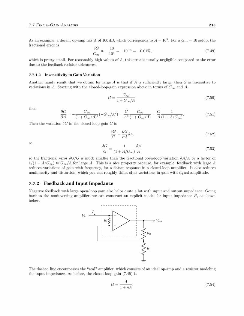
7.7 Finite-Gain Analysis 213
As an example, a decent op-amp has A of 100 dB, which corresponds to A = 105. For a G∞ = 10 setup, thefractional error is
δG
G∞
≈ − 10
105= −10−4 = −0.01%, (7.49)
which is pretty small. For reasonably high values of A, this error is usually negligible compared to the errordue to the feedback-resistor tolerances.
7.7.1.2 Insensitivity to Gain Variation
Another handy result that we obtain for large A is that if A is sufficiently large, then G is insensitive tovariations in A. Starting with the closed-loop-gain expression above in terms of G∞ and A,
G =G∞
1 + G∞/A, (7.50)
then∂G
∂A= − G∞
(1 + G∞/A)2(−G∞/A2) =
G
A2
G∞
(1 + G∞/A)=
G
A
1
(1 + A/G∞). (7.51)
Then the variation δG in the closed-loop gain G is
δG
G=
∂G
∂AδA, (7.52)
soδG
G=
1
(1 + A/G∞)
δA
A, (7.53)
so the fractional error δG/G is much smaller than the fractional open-loop variation δA/A by a factor of1/(1 + A/G∞) ≈ G∞/A for large A. This is a nice property because, for example, feedback with large Areduces variations of gain with frequency, for a flatter response in a closed-loop amplifier. It also reducesnonlinearity and distortion, which you can roughly think of as variations in gain with signal amplitude.
7.7.2 Feedback and Input Impedance
Negative feedback with large open-loop gain also helps quite a bit with input and output impedance. Goingback to the noninverting amplifier, we can construct an explicit model for input impedance Ri as shownbelow.
−
+
Vout
R2
R1
Vin
Ri
I
The dashed line encompasses the “real” amplifier, which consists of an ideal op-amp and a resistor modelingthe input impedance. As before, the closed-loop gain (7.45) is
G =A
1 + ηA. (7.54)
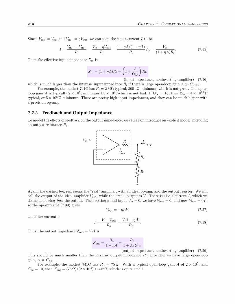
214 Chapter 7. Operational Amplifiers
Since, Vin+ = Vin, and Vin− = ηVout, we can take the input current I to be
I =Vin+ − Vin−
Ri=
Vin − ηVout
Ri=
1− ηA/(1 + ηA)
RiVin =
Vin
(1 + ηA)Ri. (7.55)
Then the effective input impedance Zin is
Zin = (1 + ηA)Ri =
(
1 +A
G∞
)
Ri,
(input impedance, noninverting amplifier) (7.56)which is much larger than the intrinsic input impedance Ri if there is large open-loop gain A≫ Ginfty.
For example, the modest 741C has Ri = 2 MΩ typical, 300 kΩ minimum, which is not great. The open-loop gain A is typically 2 × 10⁵, minimum 1.5 × 10⁴, which is not bad. If G∞ = 10, then Zin = 4 × 10¹⁰ Ωtypical, or 5× 10⁸ Ω minimum. These are pretty high input impedances, and they can be much higher witha precision op-amp.
7.7.3 Feedback and Output Impedance
To model the effects of feedback on the output impedance, we can again introduce an explicit model, includingan output resistance Ro.
−
+
V
R2
R1
Vin Ro
Vout
I
Again, the dashed box represents the “real” amplifier, with an ideal op-amp and the output resistor. We willcall the output of the ideal amplifier Vout, while the “real” output is V . There is also a current I, which wedefine as flowing into the output. Then setting a null input Vin = 0, we have Vin+ = 0, and now Vin− = ηV ,so the op-amp rule (7.39) gives
Vout = −ηAV. (7.57)
Then the current is
I =V − Vout
Ro=
V (1 + ηA)
Ro. (7.58)
Thus, the output impedance Zout = V/I is
Zout =Ro
1 + ηA=
Ro
1 + A/G∞
.
(output impedance, noninverting amplifier) (7.59)This should be much smaller than the intrinsic output impedance Ro, provided we have large open-loopgain, A≫ G∞.
For example, the modest 741C has Ro = 75 Ω. With a typical open-loop gain A of 2 × 10⁵, andG∞ = 10, then Zout = (75 Ω)/(2× 104) ≈ 4 mΩ, which is quite small.

7.7 Finite-Gain Analysis 215
7.7.4 Circuit Practice: Finite Gain in the Inverting Amplifier
For practice in dealing with finite op-amp gain, consider the noninverting amplifier, with finite open-loopgain A. (Again, it’s best to do this before continuing, so we won’t defer this until the end of the chapter.)
−
+
Vout
R2
R1
Vin
Show the following:(a) The finite-A gain is
G = − (1− η)A
1 + ηA, η :=
R1
R1 + R2.
(closed-loop gain, inverting amplifier with finite open-loop gain) (7.60)(b) Take the A −→∞ limit of Eq. (7.60) and show that
G∞ = −R2
R1.
(closed-loop gain, inverting amplifier with infinite open-loop gain) (7.61)(c) The input impedance is
Zin = R1 +R2
1 + A.
(input impedance, inverting amplifier with finite open-loop gain) (7.62)(Ignore any intrinsic input impedance of the op-amp, which we will assume is much larger than R1.)(d) The output impedance is
Zout =Ro
1 + ηA,
(input impedance, inverting amplifier with finite open-loop gain) (7.63)where Ro is the intrinsic output impedance of the op-amp, as in the noninverting case.
Solution.(a) First, the noninverting input has Vin+ = 0. The inverting input has a voltage determined by a voltagedivider between Vin and Vout:
Vin− = ηVout + (1− η)Vin. (7.64)
Remember η = R1/(R1 +R2), so as a sanity check, η −→ 1, Vin− becomes connected to Vout, and as η −→ 0,Vin− becomes connected to Vin, which makes sense. Then using Eq. (7.39),
Vout = −ηAVout − (1− η)AVin. (7.65)
Solving for Vout,
Vout = − (1− η)A
(1 + ηA)Vin. (7.66)
This is the result we wanted, with G the coefficient of Vin.(b) As A −→∞, G = −(1− η)A/(1 + ηA) −→ −(1− η)/η = −R2/R1.(c) Suppose a current I flows into the Vin terminal. Then
I =Vin − Vin−
R1=
Vin − ηVout − (1− η)Vin
R1=
η(Vin − Vout)
R1=
η[(1 + ηA) + (1− η)A]
(1 + ηA)R1Vin =
η(1 + A)
(1 + ηA)R1Vin,
(7.67)
216 Chapter 7. Operational Amplifiers
where we used the solution (7.66). Then Zin = Vin/I, so
Zin =(1 + ηA)R1
η(1 + A)=
R1
η(1 + A)+
AR1
(1 + A)=
R1 + R2
(1 + A)+
AR1
(1 + A)=
R2
(1 + A)+ R1. (7.68)
Note that this reduces to R1 as A −→∞.(d) Here, we set Vin = 0 and call the output V , with a current I going into the output terminal. Vout isthe output voltage of the ideal op-amp, before the intrinsic resistor Ro, as in the noninverting case. ThenVin− = ηV , and
Vout = A(Vin+ − Vin−) = −AVin− = −ηAV. (7.69)
So the current is
I =V − Vout
Ro=
1 + ηA
RoV, (7.70)
and so the output impedance Zout = V/I is
Zout =Ro
1 + ηA. (7.71)
Note that this decreases to zero as A −→∞.
7.8 Bandwidth
The bandwidth of an amplifier refers to the frequency range over which the response (gain) is reasonablyflat. For electronic amplifiers, one characteristic is that the gain must fall off above some frequency—noamplifier can work at arbitrarily high frequencies.
Recall that the closed-loop gain G and the open-loop gain A are related, in that the latter bounds theformer:
G ≤ A. (7.72)
Now let’s consider the frequency dependence of the gain. In particular, the open-loop gain A(ω) typicallyhas a “one-pole response,” like that of a low-pass filter:
A(ω) =A0
√
1 + (ω/ω3 dB)2. (7.73)
Here, the cutoff frequency ω3 dB = 1/RC for a low-pass filter, where R and C are typically set by intrinsictransistor resistance and stray or added (internal) capacitance in the-op-amp. Note that asymptotically,
A(ω) ∼ 1
ω(7.74)
for large ω, for a scaling of −6 dB/octave.Then the closed-loop gain is bounded by the open-loop gain, so that as the open-loop gain falls off,
so does the closed-loop gain. This is illustrated schematically below for two different dc gains G and anopen-loop gain A(ω).

7.8 Bandwidth 217
logo(w)
logo(g
ain
)
A0/w
A0Ao(w)
closed loop, largeG
Go(w)
closed loop, smallerG
Go(w)
Note that as the dc gain becomes smaller, the bandwidth (frequency range over which the gain is roughlyconstant) becomes wider. Since A cuts off as ω−1, the closed-loop gain G(ω) meets A(ω) at a frequencythat scales in the same way as ω−1. That is, the bandwidth scales as 1/G0, where G0 is the dc gain. Saiddifferently, the product of the dc gain G0 and the bandwidth is a constant, and this is often quoted asthe gain–bandwidth product (GBWP), or the unity-gain bandwidth. For example, the 741C hasa GBWP of 1.5 MHz. Generally speaking, op-amps tend to be slow, especially at high gains, compared todiscrete transistors.
7.8.1 Slew Rate
A concept closely related to bandwidth is the slew rate, which is the maximum rate of change of the output.Intuitively, this should be proportional to the GBWP, but this is somewhat more complicated because thesame signal, but with different amplitudes, would involve different slew rates, even if they have the samefrequency spectrum. So for rapidly changing signals, an op-amp with a particular slew rate may be able tofollow the signal at low amplitudes, but it may be harder for the op-amp to follow the same signal at largeramplitudes.
As a concrete example, the 741C has a modest slew rate of 0.5 V/µs. Slew rates can be much high; forexample, the BUF634 unity-gain buffer has a slew rate of 2000 V/µs.
Generally speaking, the speed of an op-amp (either in terms of slew rate or GBWP) is controlled bythe internal capacitance, which is usually fixed by an internal compensation capacitor, but also by intrinsicemitter resistance. Recalling that re ∝ 1/IC, generally speaking, a larger quiescent current (idling current)for an op-amp gives a higher slew rate or a wider GBWP. There is thus a trade-off between power andspeed—some op-amps, like the OPA602, have a programmable quiescent current so the user can chooseexactly where to make this trade-off.
7.8.1.1 Slew Rate and Power-Boosted Op-Amps
There are certain circuits where the slew rate of an op-amp is critical to its performance. One example isa “power-boosted” op-amp, where transistors are used to boost the output current capacity of an op-amp.The motivation for this circuit comes from the following “push-pull” current amplifier that we studied inSection 4.13.

218 Chapter 7. Operational Amplifiers
Vin Vout
+VCC
−VEE
To review, this is basically a stacked pair of emitter followers. The potential advantage is operation withinput signals of either polarity. The problem, though, is that one of the transistors will conduct, and theemitter (output) voltage must be a diode drop closer to zero than the base (input) voltage. That is, a graphof the output voltage responding to input voltage is schematically as in the graph below, if we assume thesimple model that the base-emitter voltage drop is a constant 0.6 V (or less).
Vout
Vin0.6 V-0.6 V
The problem in using this as an amplifier is that it leads to crossover distortion, because the base-emitterdrop changes as the signal crosses through zero. An example is shown in the graph below of crossoverdistortion of an input sine wave.
V
t
VinVinVin
Vout
One nice solution, at least in principle, is to use an op-amp, and enclose the push-pull transistor pair in thefeedback loop of the op-amp, as in the circuit below. Note the addition of a base–emitter resistor (of theorder 1 kΩ or so), which provides a feedback path when neither transistor is conducting—remember thatomitting the negative-feedback path is a good way to annoy an op-amp.

7.8 Bandwidth 219
−
+Vin
VoutVB
+VCC
−VEE
This circuit acts as a unity-gain buffer with high current-driving capacity, because the op-amp does whateverit needs to do to ensure that Vout is the same as Vin. And to do this, it must “undo” the crossover distortion,so the base voltage VB in this circuit must respond to the input as in the graph below.
VB
Vin
0.6 V
-0.6 V
This response combined with the crossover distortion results in, in principle, a distortion-free output.However, the problem with this conclusion is that it assumes that the op-amp has a long time to settle
to the “correct” value. But with a rapidly changing input signal, the op-amp must jump discontinuously by1.2 V when the input signal crosses through zero, which in practice can be problematic. This can lead tolarger distortion and “glitching” with faster input signals.
The solution to this problem that we discussed before in Section 4.13 is to bias the transistors intoconduction. However, the design of the bias-corrected circuit can be involved, especially to avoid thermalproblems and proper selection and matching of bias voltages. A handier way (but with more limited options)to solve this problem is to use a high-current buffer amplifier, where engineers have already taken care of theeffort of properly biasing the push-pull pair. One example is the circuit below, which can handle 250-mAoutput signals via a BUF634 unity-gain buffer.
−
+
BUF634
precision op-amp
Vout
Vin
The idea is to use a precision op-amp, and take the feedback from the output of the BUF634. This way,we get the high-current capacity of the “slave” BUF634, combined with the precision of the “master” op-amp. One caveat, which we will explore in more depth, is that the buffer amplifier must have a much widerbandwidth than the master op-amp.
7.8.2 Stability and Compensation
So far, we have talked about the frequency-dependent gain, but the frequency-dependent phase is also critical.As we have noted, for most purposes we can regard an op-amp as having a gain behavior similar to a low-pass

220 Chapter 7. Operational Amplifiers
filter.Recall that for an RC filter, the relative phase of the output is 0 in the limit ω −→ 0, and changes
to a 90 phase lag as ω −→ ∞. If we have multiple, cascaded filters, at high frequencies, intuitively we canthink of having a 90 phase per “pole”, or roughly speaking, per RC pair. This can pose a problem forop-amp circuits that require negative feedback. Due to phase shifts and time delays in the feedback loopat high frequencies can add up to a 180 phase shift. However, negative feedback in combination with aphase shift of 180 (or in fact anything between 90 and 270) is in fact positive feedback. This can turninto unstable behavior (oscillation) if the gain of the circuit exceeds unity in the frequency range where thefeedback becomes positive feedback.
Thus comes the idea of compensation. Most op-amps include an internal capacitor to “roll off” thegain, and in particular to ensure that the gain is less than unity at frequencies where large phase shiftsmay cause problems. There are also uncompensated op-amps, which need an external capacitor or anappropriate reactive load to achieve stability. An example is the inverting amplifier below, with an explicitcompensation capacitor to cut off the gain at high frequencies.
−
+
Vout
R2
compensation C
R1
Vin
Another example is a variation on the BUF634 buffered op-amp circuit from the previous section. If theslave buffer amplifier is slower than the master op-amp, this may cause a problem because the phase shiftdue to the slower buffer may cause the master to become unstable or oscillate. A solution to use a slowbuffer is the circuit below.
−
+
precision op-ampslow buffer
Vout
R
Vin
C
For small frequencies (ω ≪ ω3 dB = 1/RC), the feedback comes from the buffer output, while at high fre-quencies (ω ≫ ω3 dB = 1/RC), the feedback comes from the output of the master op-amp. This arrangementavoids problems with the phase shift and maintains stability of the amplifier.
7.8.2.1 Op-Amp Output and Capacitive Loads
To examine a problematic situation in a bit more detail, let’s return to the bandwidth argument of Section 7.8,but now keep the complex phase in the open-loop gain:
A(ω) =A0
1− iω/ω3 dB. (7.75)
Again, this response has the form of a low-pass filter [Eq. (2.44)], where the op-amp response “rolls off” dueto a single capacitor. Then, taking the example of the noninverting amplifier of Section 7.7.3, the op-amp
7.9 Comparators 221
output impedance (7.59) becomes
Zout(ω) =Ro
1 + A(ω)/G∞
=Ro(1− iω/ω3 dB)
1 + A0/G∞ − iω/ω3 dB.
(output impedance, noninverting amplifier) (7.76)Since typically A0 ≫ G∞, we can consider the intermediate range of frequencies between ω3 dB and (A0/G∞) ω3 dB,where the impedance reduces to
Zout(ω) =Ro(−iω/ω3 dB)
A0/G∞
= −iωRoG∞
ω3 dBA0
(
1≪ ω
ω3 dB≪ A0
G∞
)
. (7.77)
This has the form of an inductive reactance [see Eq. (2.40)], with effective inductance
Leff =RoG∞
ω3 dBA0. (7.78)
This inductive regime can span a wide range. With ω3 dB/2π ∼ 100 Hz, Ro ∼ 100 Ω, A0 ∼ 106, and G∞ = 10,this works out to a frequency range of ∼100 Hz to ∼10 MHz, with an effective inductance of ∼1.6 µH.
Outside this frequency band, the output impedance is simply resistive. For small frequencies, we have
Zout(ω) =Ro
1 + A0/G∞
(
ω
ω3 dB≪ 1 <
A0
G∞
)
, (7.79)
while for very large frequencies,
Zout(ω) = Ro
(
1 <A0
G∞
≪ ω
ω3 dB
)
. (7.80)
Note that in practice, other stray capacitances will become important in the high-frequency range.The inductive output of the op-amp in the regime of Eq. (7.77) can give rise to problems if the output
of the op-amp drives a capacitive load. Then Leff and the capacitance form a resonant circuit. This can leadto a resonant peak in the gain profile at frequency
ω0 =1√
LeffC=
√
ω3 dBA0
RoCG∞
. (7.81)
For the same parameters, this would lead to a resonance at ω/2π ∼ 100 kHz for a load capacitance C = 1 µF.If the effect of the resonance is sufficiently strong (i.e., sufficiently large Q), the circuit can become unstableand oscillate near this resonance frequency.
7.9 Comparators
Recall that op-amps are basically high-gain differential amplifiers.
−
+
Vout = A(Vin+ − Vin−)
Vin+
Vin−
We have mostly concentrated on closed-loop operation (feedback from output to the inverting input), whichforces the inputs to have basically the same voltage. In open-loop operation (no feedback), the inputs arenot the same, and if they are different by even a small amount (∼mV), the output rails one way or theother to reflect the difference. This open-loop operation is useful in some contexts, and op-amps that arespecifically designed for this purpose are called comparators.
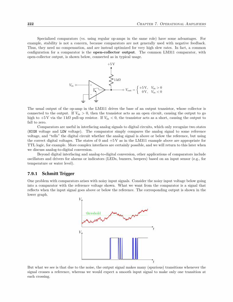
222 Chapter 7. Operational Amplifiers
Specialized comparators (vs. using regular op-amps in the same role) have some advantages. Forexample, stability is not a concern, because comparators are not generally used with negative feedback.Thus, they need no compensation, and are instead optimized for very high slew rates. In fact, a commonconfiguration for a comparator is the open-collector output. The common LM311 comparator, withopen-collector output, is shown below, connected as in typical usage.
−
+
Vout =
+5 V, Vin > 00 V, Vin < 0
1 kΩ
+5 V
Vin
The usual output of the op-amp in the LM311 drives the base of an output transistor, whose collector isconnected to the output. If Vin > 0, then the transistor acts as an open circuit, causing the output to gohigh to +5 V via the 1 kΩ pull-up resistor. If Vin < 0, the transistor acts as a short, causing the output tofall to zero.
Comparators are useful in interfacing analog signals to digital circuits, which only recognize two states(HIGH voltage and LOW voltage). The comparator simply compares the analog signal to some referencevoltage, and “tells” the digital circuit whether the analog signal is above or below the reference, but usingthe correct digital voltages. The states of 0 and +5 V as in the LM311 example above are appropriate forTTL logic, for example. More complex interfaces are certainly possible, and we will return to this later whenwe discuss analog-to-digital conversion.
Beyond digital interfacing and analog-to-digital conversion, other applications of comparators includeoscillators and drivers for alarms or indicators (LEDs, buzzers, beepers) based on an input sensor (e.g., fortemperature or water level).
7.9.1 Schmitt Trigger
One problem with comparators arises with noisy input signals. Consider the noisy input voltage below goinginto a comparator with the reference voltage shown. What we want from the comparator is a signal thatreflects when the input signal goes above or below the reference. The corresponding output is shown in thelower graph.
V
t
threshold
V
t
But what we see is that due to the noise, the output signal makes many (spurious) transitions whenever thesignal crosses a reference, whereas we would expect a smooth input signal to make only one transition ateach crossing.
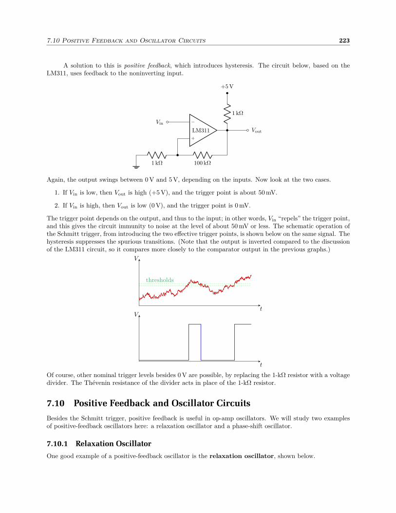
7.10 Positive Feedback and Oscillator Circuits 223
A solution to this is positive feedback, which introduces hysteresis. The circuit below, based on theLM311, uses feedback to the noninverting input.
−
+
LM311 Vout
1 kΩ
+5 V
Vin
100 kΩ1 kΩ
Again, the output swings between 0 V and 5 V, depending on the inputs. Now look at the two cases.
1. If Vin is low, then Vout is high (+5 V), and the trigger point is about 50 mV.
2. If Vin is high, then Vout is low (0 V), and the trigger point is 0 mV.
The trigger point depends on the output, and thus to the input; in other words, Vin “repels” the trigger point,and this gives the circuit immunity to noise at the level of about 50 mV or less. The schematic operation ofthe Schmitt trigger, from introducing the two effective trigger points, is shown below on the same signal. Thehysteresis suppresses the spurious transitions. (Note that the output is inverted compared to the discussionof the LM311 circuit, so it compares more closely to the comparator output in the previous graphs.)
V
t
thresholds
V
t
Of course, other nominal trigger levels besides 0 V are possible, by replacing the 1-kΩ resistor with a voltagedivider. The Thévenin resistance of the divider acts in place of the 1-kΩ resistor.
7.10 Positive Feedback and Oscillator Circuits
Besides the Schmitt trigger, positive feedback is useful in op-amp oscillators. We will study two examplesof positive-feedback oscillators here: a relaxation oscillator and a phase-shift oscillator.
7.10.1 Relaxation Oscillator
One good example of a positive-feedback oscillator is the relaxation oscillator, shown below.
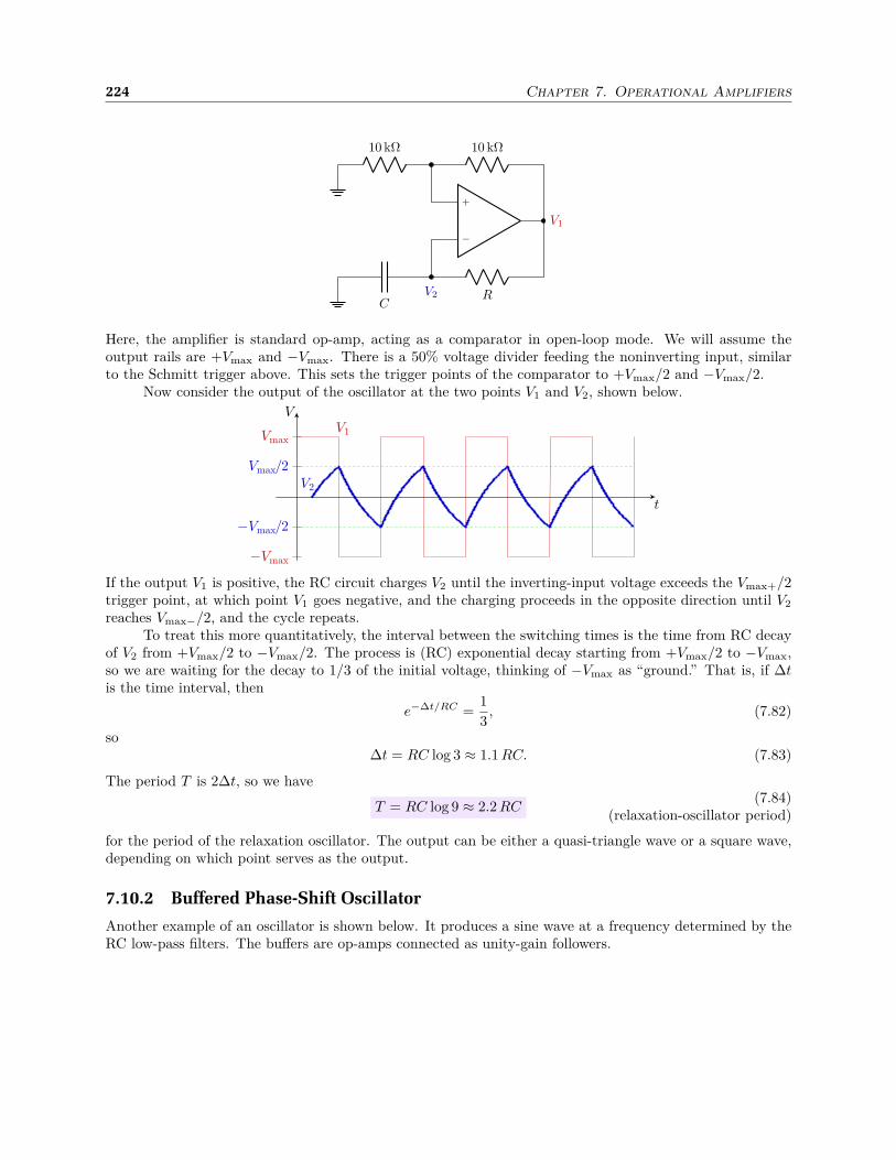
224 Chapter 7. Operational Amplifiers
−
+
V1
10 kΩ10 kΩ
RC
V2
Here, the amplifier is standard op-amp, acting as a comparator in open-loop mode. We will assume theoutput rails are +Vmax and −Vmax. There is a 50% voltage divider feeding the noninverting input, similarto the Schmitt trigger above. This sets the trigger points of the comparator to +Vmax/2 and −Vmax/2.
Now consider the output of the oscillator at the two points V1 and V2, shown below.
V
t
Vmax
/2
-Vmax
/2
Vmax
-Vmax
V1
V2
If the output V1 is positive, the RC circuit charges V2 until the inverting-input voltage exceeds the Vmax+/2trigger point, at which point V1 goes negative, and the charging proceeds in the opposite direction until V2
reaches Vmax−/2, and the cycle repeats.To treat this more quantitatively, the interval between the switching times is the time from RC decay
of V2 from +Vmax/2 to −Vmax/2. The process is (RC) exponential decay starting from +Vmax/2 to −Vmax,so we are waiting for the decay to 1/3 of the initial voltage, thinking of −Vmax as “ground.” That is, if ∆tis the time interval, then
e−∆t/RC =1
3, (7.82)
so∆t = RC log 3 ≈ 1.1 RC. (7.83)
The period T is 2∆t, so we have
T = RC log 9 ≈ 2.2 RC(7.84)
(relaxation-oscillator period)
for the period of the relaxation oscillator. The output can be either a quasi-triangle wave or a square wave,depending on which point serves as the output.
7.10.2 Buffered Phase-Shift Oscillator
Another example of an oscillator is shown below. It produces a sine wave at a frequency determined by theRC low-pass filters. The buffers are op-amps connected as unity-gain followers.
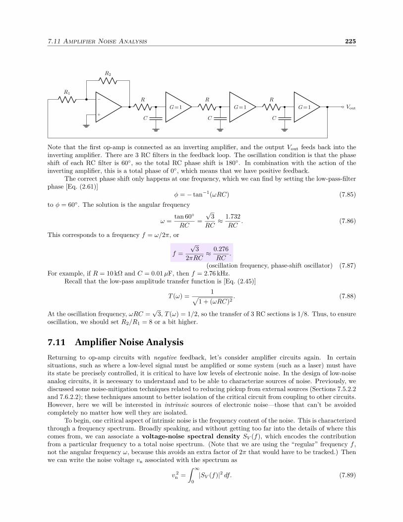
7.11 Amplifier Noise Analysis 225
−
+
R2
R1
G=1 G=1 G=1
R
C
R
C
R
C
Vout
Note that the first op-amp is connected as an inverting amplifier, and the output Vout feeds back into theinverting amplifier. There are 3 RC filters in the feedback loop. The oscillation condition is that the phaseshift of each RC filter is 60, so the total RC phase shift is 180. In combination with the action of theinverting amplifier, this is a total phase of 0, which means that we have positive feedback.
The correct phase shift only happens at one frequency, which we can find by setting the low-pass-filterphase [Eq. (2.61)]
φ = − tan−1(ωRC) (7.85)
to φ = 60. The solution is the angular frequency
ω =tan 60
RC=
√3
RC≈ 1.732
RC. (7.86)
This corresponds to a frequency f = ω/2π, or
f =
√3
2πRC≈ 0.276
RC.
(oscillation frequency, phase-shift oscillator) (7.87)For example, if R = 10 kΩ and C = 0.01 µF, then f = 2.76 kHz.
Recall that the low-pass amplitude transfer function is [Eq. (2.45)]
T (ω) =1
√
1 + (ωRC)2. (7.88)
At the oscillation frequency, ωRC =√
3, T (ω) = 1/2, so the transfer of 3 RC sections is 1/8. Thus, to ensureoscillation, we should set R2/R1 = 8 or a bit higher.
7.11 Amplifier Noise Analysis
Returning to op-amp circuits with negative feedback, let’s consider amplifier circuits again. In certainsituations, such as where a low-level signal must be amplified or some system (such as a laser) must haveits state be precisely controlled, it is critical to have low levels of electronic noise. In the design of low-noiseanalog circuits, it is necessary to understand and to be able to characterize sources of noise. Previously, wediscussed some noise-mitigation techniques related to reducing pickup from external sources (Sections 7.5.2.2and 7.6.2.2); these techniques amount to better isolation of the critical circuit from coupling to other circuits.However, here we will be interested in intrinsic sources of electronic noise—those that can’t be avoidedcompletely no matter how well they are isolated.
To begin, one critical aspect of intrinsic noise is the frequency content of the noise. This is characterizedthrough a frequency spectrum. Broadly speaking, and without getting too far into the details of where thiscomes from, we can associate a voltage-noise spectral density SV (f), which encodes the contributionfrom a particular frequency to a total noise spectrum. (Note that we are using the “regular” frequency f ,not the angular frequency ω, because this avoids an extra factor of 2π that would have to be tracked.) Thenwe can write the noise voltage vn associated with the spectrum as
v 2n =
∫ ∞
0
|SV (f)|2 df. (7.89)
226 Chapter 7. Operational Amplifiers
That is, the voltage noise should be thought of as a (hopefully small), fluctuating voltage signal; vn charac-terizes its size in the root-mean-square sense as
vn =
√
v2(t) , (7.90)
where v(t) is the explicit, time-dependent noise signal, and the bar ( ) denotes a time average. FromEq. (7.89), the dimensions of SV (ω) must be V/
√Hz, an odd-looking unit that commonly comes up in noise
analysis (and op-amp data sheets). Correspondingly, one can write down an analogous relation for the rmscurrent noise in in terms of a noise spectrum SI(f) as
i 2n =
∫ ∞
0
|SI(f)|2 df, (7.91)
where SI(f) is measured in A/√
Hz. If the voltage refers to a difference across a pure resistance R, thenthe two noise quantities are related by vn = inR. More generally, however, if there is a frequency-dependentimpedance Z(f), we should instead write
SV (f) = SI(f)Z(f), (7.92)
because it is the noise spectra that are related, with the impedance affecting each frequency differently.It’s worth elaborating on a couple of details before continuing. First, from Eq. (7.92), evidently the
spectra may be complex functions. There are some subtleties in handling this properly, but for our purposesthis is irrelevant; any complex phase will get discarded in computing the magnitude of the noise signals inEqs. (7.89) or (7.91). The second, related detail is in the squaring of the spectrum before we sum over thecontributions of different frequencies. There are a couple of useful ways to think about this. First, sincethese are noise fluctuations associated with different frequencies, the signals at different frequencies shouldnot have any special phase relation, and so it is the power or energy of the different components that shouldadd, not the voltage or current. [More mundanely, adding different frequency components and then squaringto find the energy only gives extra “cross” terms of the form sin(2πf1t) sin(2πf2t), which average to zeroafter enough time if f1 6= f2.] However, it is also worth noting that this adding of squared signals mirrorswhat happens when you combine independent, random quantities: they add in quadrature. To see whatwe mean by this, consider two random variables X1 and X2. For simplicity, suppose they have zero mean(but a similar argument carries through for nonzero mean): X1 = X2 = 0. Then the variance of the sumX1 + X2 is
(X1 + X2)2 = X 21 + X 2
2 + 2X1X2 = X 21 + X 2
2 + 2X1 X2 = X 21 + X 2
2 , (7.93)
where we used X1X2 = X1 X2 for independent random variables. This means that the variances of randomvariables add. (This is the same idea behind error-propagation, adding independent contributions to thetotal statistical error.) In the case of summing over a spectrum in Eq. (7.89), you can think of each frequencycomponent as something like a random variable, because it is a quantity varying sinusoidally, but with somerandom phase. The total fluctuation at any time is the sum over all of these “random” contributions, butthese contribution should be added in quadrature to characterize their magnitude.
7.11.1 Sources of Noise
There are many intrinsic sources of noise, but we will discuss only the most important ones to worry about(at least for intrinsic noise).
7.11.1.1 Johnson–Nyquist Noise
One of the most important sources of noise in circuits is associated with thermal motion of electrons inresistive materials. The associated noise goes by the name of Johnson noise or Johnson–Nyquist noise.3
3Johnson noise is so named after the first person to measure it: J. B. Johnson, “Thermal Agitation of Electricity inConductors,” Physical Review Letters 32, 97 (1928) (doi: 10.1103/PhysRev.32.97). It is also called Johnson–Nyquist noise,named additionally after the first to describe it theoretically: H. Nyquist, “Thermal Agitation of Electric Charge in Conductors,”Physical Review Letters 32, 110 (1928) (doi: 10.1103/PhysRev.32.110).
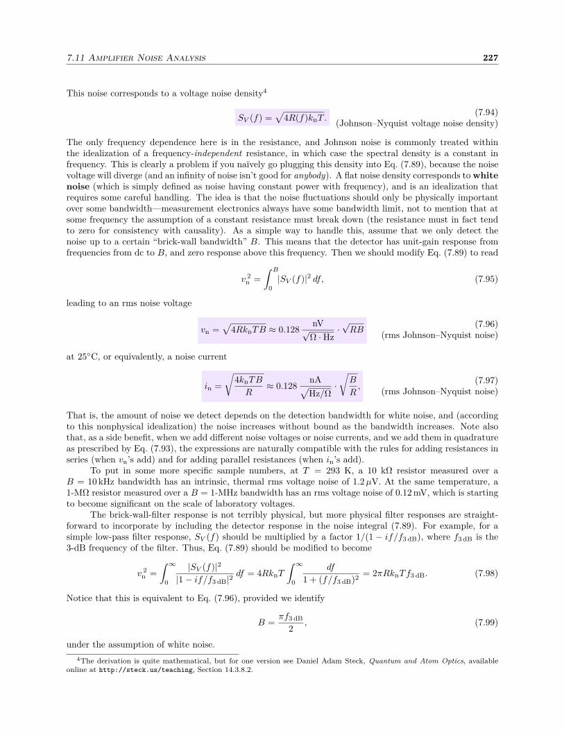
7.11 Amplifier Noise Analysis 227
This noise corresponds to a voltage noise density4
SV (f) =√
4R(f)kBT .(7.94)
(Johnson–Nyquist voltage noise density)
The only frequency dependence here is in the resistance, and Johnson noise is commonly treated withinthe idealization of a frequency-independent resistance, in which case the spectral density is a constant infrequency. This is clearly a problem if you naïvely go plugging this density into Eq. (7.89), because the noisevoltage will diverge (and an infinity of noise isn’t good for anybody). A flat noise density corresponds to whitenoise (which is simply defined as noise having constant power with frequency), and is an idealization thatrequires some careful handling. The idea is that the noise fluctuations should only be physically importantover some bandwidth—measurement electronics always have some bandwidth limit, not to mention that atsome frequency the assumption of a constant resistance must break down (the resistance must in fact tendto zero for consistency with causality). As a simple way to handle this, assume that we only detect thenoise up to a certain “brick-wall bandwidth” B. This means that the detector has unit-gain response fromfrequencies from dc to B, and zero response above this frequency. Then we should modify Eq. (7.89) to read
v 2n =
∫ B
0
|SV (f)|2 df, (7.95)
leading to an rms noise voltage
vn =√
4RkBTB ≈ 0.128nV√
Ω ·Hz·√
RB(7.96)
(rms Johnson–Nyquist noise)
at 25C, or equivalently, a noise current
in =
√
4kBTB
R≈ 0.128
nA√
Hz/Ω·√
B
R,
(7.97)(rms Johnson–Nyquist noise)
That is, the amount of noise we detect depends on the detection bandwidth for white noise, and (accordingto this nonphysical idealization) the noise increases without bound as the bandwidth increases. Note alsothat, as a side benefit, when we add different noise voltages or noise currents, and we add them in quadratureas prescribed by Eq. (7.93), the expressions are naturally compatible with the rules for adding resistances inseries (when vn’s add) and for adding parallel resistances (when in’s add).
To put in some more specific sample numbers, at T = 293 K, a 10 kΩ resistor measured over aB = 10 kHz bandwidth has an intrinsic, thermal rms voltage noise of 1.2 µV. At the same temperature, a1-MΩ resistor measured over a B = 1-MHz bandwidth has an rms voltage noise of 0.12 mV, which is startingto become significant on the scale of laboratory voltages.
The brick-wall-filter response is not terribly physical, but more physical filter responses are straight-forward to incorporate by including the detector response in the noise integral (7.89). For example, for asimple low-pass filter response, SV (f) should be multiplied by a factor 1/(1 − if/f3 dB), where f3 dB is the3-dB frequency of the filter. Thus, Eq. (7.89) should be modified to become
v 2n =
∫ ∞
0
|SV (f)|2|1− if/f3 dB|2
df = 4RkBT
∫ ∞
0
df
1 + (f/f3 dB)2= 2πRkBTf3 dB. (7.98)
Notice that this is equivalent to Eq. (7.96), provided we identify
B =πf3 dB
2, (7.99)
under the assumption of white noise.
4The derivation is quite mathematical, but for one version see Daniel Adam Steck, Quantum and Atom Optics, availableonline at http://steck.us/teaching, Section 14.3.8.2.

228 Chapter 7. Operational Amplifiers
7.11.1.2 “kT/C” Noise
Another noise that is basically just Johnson noise is associated with capacitance. Consider an R–C low-passfilter, and recall that the filter’s corner frequency is, from Eq. (2.47),
f3 dB =1
2πRC. (7.100)
Putting this into Eq. (7.98) gives
vn =
√
kBT
C≈ 64.2 nV ·
√µF√
C.
(7.101)(kBT/C noise)
at 25C. Surprisingly, the dependence on the resistance cancels completely out, so the result is effectivelyassociated with only the capacitance. But, of course, some kind of resistance must be present to generatethe noise—reactances don’t generate Johnson noise, only resistive impedances. Intuitively, a larger resis-tance creates more noise, but the noise is filtered to a narrower bandwidth by the smaller cutoff frequency.Importantly, larger capacitances are associated with lower noise,
7.11.1.3 Shot Noise
Another type of noise is associated with flowing current: you might think of electrical current as a smoothflow (like the flow of water), but the current itself is the motion of discrete charge carriers. So if you sit ata certain point on a wire and watch current flowing past (to the extent this is possible), with the “smoothcurrent,” the charge that passes by you rises linearly with time: Q(t) = It. However, counting the discretepassage of electrons instead, Q(t) rises in little jumps, and it’s only the average slope that works out to I.This intrinsic noise in the current is called shot noise, and to a good approximation shot noise behaves aswhite noise (provided many carriers are passing by in any given observation time). The current shot noiseis5
in =√
2|eI|B,(7.102)
(current shot-noise)
where e is the electron charge, I is the (mean) current, and B is again the brick-wall bandwidth. Thisexpression assumes that the electrons in the current arrive independently; if electron motion is correlated,this can affect the magnitude of the shot noise. Shot noise is an important effect in, for example, vacuumtubes and in semiconductor-junction devices, or in any sitation that is sensitive to current noise.
Shot noise applies in other situations where there is a mean flow of discrete particles. For example,laser light comes in discrete photons of energy ~ω, where ω is the optical frequency. Adapting the formula(7.102) gives
δP =√
2~ωPB(7.103)
(optical shot-noise)
as the rms power fluctuation, given a mean optical power P .
7.11.1.4 1/f Noise
Another important class of noise is 1/f noise, which has a spectral density of the form
SV (f) =
√
k
f,
(7.104)(1/f noise density)
for some constant k. Note that the noise is so named because the noise power density (i.e., SV 2). Thisnoise, also called pink noise or flicker noise, was first noticed as a component of the shot noise in a
5For more details, see Daniel Adam Steck, Quantum and Atom Optics, available online at http://steck.us/teaching,Section 17.5.3.1.
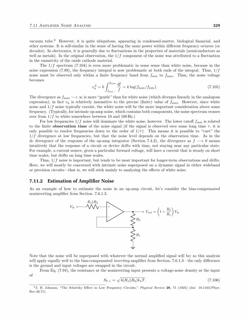
7.11 Amplifier Noise Analysis 229
vacuum tube.6 However, it is quite ubiquitous, appearing in condensed-matter, biological financial, andother systems. It is self-similar in the sense of having the same power within different frequency octaves (ordecades). In electronics, it is generally due to fluctuations in the properties of materials (semiconductors aswell as metals). In the original observation, the 1/f component of the noise was attributed to a fluctuationin the emissivity of the oxide cathode material.
The 1/f spectrum (7.104) is even more problematic in some sense than white noise, because in thenoise expression (7.89), the frequency integral is now problematic at both ends of the integral. Thus, 1/fnoise must be observed only within a finite frequency band from fmin to fmax. Thus, the noise voltagebecomes
v 2n = k
∫ fmax
fmin
df
f= k log(fmax/fmin). (7.105)
The divergence as fmax −→∞ is more “gentle” than for white noise (which diverges linearly in the analogousexpression); in fact vn is relatively insensitive to the precise (finite) value of fmax. However, since whitenoise and 1/f noise typically coexist, the white noise will be the more important consideration above somefrequency. (Typically, for intrinsic op-amp noise, which contains both components, the noise spectrum crossesover from 1/f to white somewhere between 10 and 100 Hz.)
For low frequencies 1/f noise will dominate the white noise, however. The lower cutoff fmin is relatedto the finite observation time of the noise signal (if the signal is observed over some long time τ , it isonly possible to resolve frequencies down to the order of 1/τ). This means it is possible to “cure” the1/f divergence at low frequencies, but that the noise level depends on the observation time. As in thedc divergence of the response of the op-amp integrator (Section 7.4.2), the divergence as f −→ 0 meansintuitively that the response of a circuit or device drifts with time, not staying near any particular state.For example, a current source, given a particular forward voltage, will have a current that is steady on shorttime scales, but drifts on long time scales.
Thus, 1/f noise is important, but tends to be most important for longer-term observations and drifts.Here, we will mostly be concerned with intrinsic noise superposed on a dynamic signal in either widebandor precision circuits—that is, we will stick mainly to analyzing the effects of white noise.
7.11.2 Estimation of Amplifier Noise
As an example of how to estimate the noise in an op-amp circuit, let’s consider the bias-compensatednoninverting amplifier from Section. 7.6.1.3.
−
+
Vout =
(
1 +R2
R1
)
Vin
R2
R1
R1‖R2
Vin
Note that the noise will be superposed with whatever the normal amplified signal will be; so this analysiswill apply equally well to the bias-compensated inverting amplifier from Section. 7.6.1.3—the only differenceis the ground and input voltages are swapped in the circuit.
From Eq. (7.94), the resistance at the noninverting input presents a voltage-noise density at the inputof
SV + =√
4(R1‖R2)kBT . (7.106)
6J. B. Johnson, “The Schottky Effect in Low Frequency Circuits,” Physical Review 26, 71 (1925) (doi: 10.1103/Phys-Rev.26.71).

230 Chapter 7. Operational Amplifiers
The Thévenin equivalent circuit for the voltage divider presents the same resistance to the inverting input,so we get the same noise density there:
SV − =√
4(R1‖R2)kBT . (7.107)
The op-amp itself will have intrinsic noise; this will generally be specified as a voltage and current noise,referenced to the inputs (that is, noise voltage and current as if they are fed to the input). The op-ampvoltage noise, SV opamp, will add to the Johnson noises. In this circuit, the op-amp current noise SIin willcontribute to the noise by being converted to voltage noise by the input impedances: each input will see anextra SIopamp(R1‖R2) of voltage noise.
All of these components add together to give a total input-referenced voltage noise density of
SV in =√
S 2V + + S 2
V − + S 2V opamp + 2S 2
Iopamp(R1‖R2)2
=√
8(R1‖R2)kBT + S 2V opamp + 2S 2
Iopamp(R1‖R2)2.(7.108)
Note the factor of 2 in the last term, corresponding to adding uncorrelated noise sources. There is somesubtlety here, because the input current noise of an op-amp will generally have both incoherent and coher-ent parts. For example, for a bipolar-input op-amp, if we refer back to the BJT differential amplifier inSection 4.10.4, the current source in the “long tail” contributes current noise that is split between the twoinput transistors; thus this noise is correlated. In more sophisticated op-amps like the LT1028, there is aninput-bias cancelling circuit that injects current into the bases of the input transistors, trying to minimizethe bias current from the op-amp inputs; this system also results in correlated current noise into the inputs.On the other hand, both input transistors will have their own shot noise, which is an example of uncorrelated
noise. Recall that the rule above for adding noise sources in quadrate applies to uncorrelated noise sources;correlated noises simply add. The correlated current noises would lead to a factor of 4 instead of 2 in the lastterm under the radical of Eq. (7.108). In this case, we assume the current noise to be uncorrelated becausethe input impedances are balanced, so any correlated input current noise gets translated into common-modevoltage noise, which is rejected by the op-amp (the data sheet confirms that the 1 pA/
√Hz figure corresponds
to balanced input impedance). Unfortunately it is sometimes hard to tell whether or not the current noiseis correlated, but note that the LT1028 data sheet gives input current noise plots for both matched andunmatched source resistances (when the input resistances are far unmatched, it is better to treat the noisesas correlated). But in any case, this can be another advantage to having an input-impedance-matchingresistor as in Sections 7.6.1.2 and 7.6.1.3, at least if the reduction in the effect of input current noise is moresignificant than the added Johnson noise.
At the output of the op-amp, the noise density will simply be the input-referenced noise densitymultiplied by the circuit gain:
SV out = GSV in =
(
1 +R2
R1
)
√
S 2V + + S 2
V − + S 2V opamp + 2S 2
Iopamp(R1‖R2)2. (7.109)
To continue at this point, we will need to be more specific with example numbers. Suppose we take R1 =100 Ω, R2 = 100 kΩ, so that R1‖R2 ≈ 100 Ω, and G = 1001. Suppose also that we choose the LT1028low-noise, wide-band op-amp.7 For this amplifier, at 25C and 1 kHz (and for the better LT1028AM/ACvariant), SV opamp = 0.85 nV/
√Hz, and SIopamp = 1.0 pA/
√Hz. Then the magnitudes of the various noise
components is
SV + = SV − = 1.28nV√Hz
, SV opamp = 0.85nV√Hz
, SIopamp(R1‖R2) = 0.1nV√Hz
. (7.110)
In this example, the resistor thermal noise is the most important, and the op-amp current noise is almostnegligible. Computing the final noise at the output gives
SV out = 2.0µV√Hz
. (7.111)
7http://cds.linear.com/docs/en/datasheet/1028fd.pdf. Note that the numbers in the example here match those of thenoise calculations in the noise example there.
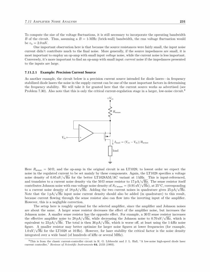
7.11 Amplifier Noise Analysis 231
To compute the size of the voltage fluctuations, it is still necessary to incorporate the operating bandwidthB of the circuit. Thus, assuming a B = 1-MHz (brick-wall) bandwidth, the rms voltage fluctuation wouldbe vn = 2.0 mV.
One important observation here is that because the source resistances were fairly small, the input noisecurrent didn’t contribute much to the final noise. More generally, if the source impedances are small, it ismost important to employ an op-amp with small input voltage noise, while the current noise is less important.Conversely, it’s more important to find an op-amp with small input current noise if the impedances presentedto the inputs are large.
7.11.2.1 Example: Precision Current Source
As another example, the circuit below is a precision current source intended for diode lasers—in frequencystabilized diode lasers the noise in the supply current can be one of the most important factors in determiningthe frequency stability. We will take it for granted here that the current source works as advertised (seeProblem 7.30). Also note that this is only the critical current-regulation stage in a larger, low-noise circuit.8
−
+
Rsense
+VSS
Vin
load
Iload = (VSS − Vin)/Rsense
Here Rsense = 50 Ω, and the op-amp in the original circuit is an LT1028; to lowest order we expect thenoise in the regulated current to be set mainly by these components. Again, the LT1028 specifies a voltagenoise density of 0.85 nV/
√Hz for the better LT1028AM/AC variant at 1 kHz. This is input-referenced,
and translates to a current noise density via the 50 Ω sense resistor to 17 pA/√
Hz. The sense resistor itselfcontributes Johnson noise with rms voltage noise density of SV sense = (0.91 nV/
√Hz), at 25C, corresponding
to a current noise density of 18 pA/√
Hz. Adding the two current noises in quadrature gives 25 pA/√
Hz.Note that the 1 pA/
√Hz input noise current density should also be added (in quadrature) to this result,
because current flowing through the sense resistor also can flow into the inverting input of the amplifier.However, this is a negligible correction.
The setup here is roughly optimal for the selected amplifier, since the amplifier and Johnson noisesare about the same. A larger sense resistor decreases the effect of the amplifier noise, but increases theJohnson noise. A smaller sense resistor has the opposite effect. For example, a 30 Ω sense resistor increasesthe effective amplifier noise to 28 pA/
√Hz, while decreasing the Johnson noise to 0.70 nV/
√Hz, which is
equivalent to 23 pA/√
Hz. The total is then 36 pA/√
Hz, which is worse off, at least using the 1-kHz noisefigure. A smaller resistor may better optimize for larger noise figures at lower frequencies (for example,1.0 nV/
√Hz for the LT1028 at 10 Hz). However, for laser stability the critical factor is the noise density
integrated over a wide band (of hundreds of kHz or several MHz).
8This is from the classic current-controller circuit in K. G. Libbrecht and J. L. Hall, “A low-noise high-speed diode lasercurrent controller,” Reviews of Scientific Instruments 64, 2133 (1993).

232 Chapter 7. Operational Amplifiers
One curiosity of the original circuit is a pair of diodes in the power-supply lines of the op-amp. Thediodes on the power-supply inputs don’t directly help with noise suppression, but rather are there forprotection of the op-amp inputs. For ultralow-noise amplifiers like the LT1028 or AD797, the inputs don’thave current-limiting input resistors, but have back-to-back protection diodes. The diodes help to protectthe inputs in situations where the amplifier is unpowered (or unusually powered, as in turn-on or turn-offtransients).9
A final thing to check here is that the control voltage Vin is subject to noise, as it is derived from avoltage divider referenced to +VSS. The output of the voltage divider is bypassed by a 22-µF capacitor, soa good estimate of the noise comes from the kBT/C noise in Eq. (7.98), which amounts to an rms noise ofvn = 14 nV. To compare this to the op-amp input voltage noise, we must invoke a bandwidth. For a roughestimate, suppose we take B = 1 MHz, in which case the input voltage noise of the op-amp is 0.85 µV (i.e.,after multiplying by
√B). On this scale, the control-voltage noise is negligible (and of course can always be
made smaller by choosing a larger bypass capacitor).If you’ve been paying attention, you might remember that the MOSFET (here specified as a VP010610)
acts something like a variable resistor—but to good approximation we are completely ignoring it in thisanalysis. (Why?) (Hint: this is only true assuming the op-amp is doing its job.) The original circuit alsohas a couple of resistors at the output of the capacitor (a 10-kΩ resistor connecting the op-amp output tothe MOSFET gate, and a 100-Ω resistor in series with a capacitor to “load” the gate). But we can ignorethose too. (Why?)
The noise estimate here is good as a first cut, but life is more complicated because of the gate capaci-tance interacting with the finite gain of the op-amp, as modeled in Problem 7.30; these factors combine toproduce resonant behavior, which can boost the current noise in the related frequency band.11
Input-stage noise. The same current source has a modulation-input stage that allows relatively fastmodulation of the current via an external control voltage (to sweep the laser current or to modulate it foruse in lock-in detection). This input stage is shown below, and the output current Iout is simply added tothe current of the main regulating circuit above. This circuit regulates the current to Iout = Vin/(1 kΩ),independent of Vout (which depends on the load); the circuit also functions properly when no input isconnected (setting Iout = 0). For the analysis of this circuit, see Problem 7.25.
−
+
−
+
1 kΩ
1 kΩ
1 kΩ
Vout
1 kΩ
2 kΩ
Vin
1 kΩ
1 µF
1 kΩ
1 kΩ
Iout
IC1
IC2
To analyze the noise here, first consider the noise contributed by the IC1 portion of the circuit. IC1 seesan input resistance of 500 Ω at the inverting input, corresponding to 2.9 nV/
√Hz of Johnson noise. The
9This is explained in more detail in John Ardizzoni, “Protecting Off-Amps” http://www.analog.com/library/
analogdialogue/archives/42-10/off_amps.html10http://ww1.microchip.com/downloads/en/DeviceDoc/VP0106%20C082313.pdf11For further analysis with noise measurements, see Chris Seck, Paul J. Martin, Eryn C. Cook, Brian Odom, and Daniel
A. Steck, “Noise reduction of a Libbrecht–Hall-style current driver,” Review of Scientific Instruments 87, 064703 (2016) (doi:10.1063/1.4953330) (arXiv: 1604.00374).

7.11 Amplifier Noise Analysis 233
op-amps are OP27’s, with 3.0 nV/√
Hz at 1 kHz for the better (OP27A/E) grade, and an input noise currentdensity of 0.4 pA/
√Hz. Then the total input-referenced noise is 4.2 nV/
√Hz, and thus 8.4 nV/
√Hz at IC1’s
output due to the noninverting gain of 2. Across the 1-kΩ resistor to Vout, this converts to 8.4 pA/√
Hz ofcurrent noise. Adding this to the 4.0 pA/
√Hz Johnson noise of the resistor itself gives 9.3 pA/
√Hz current
noise for the IC1 section. Note that IC1’s input noise current should also contribute directly to the Iout
noise, but this contribution is negligible. Notice that adding this current density to the 25 pA/√
Hz noisefrom the main regulating amplifier only increases the noise by about 7%, to 27 pA/
√Hz.
That is the noise estimate assuming that the input is held fixed by a noiseless source. With a discon-nected input voltage, IC2 also contributes to the current noise. IC2 sees Johnson noises of 2.9 nV/
√Hz and
4.0 nV/√
Hz at the inverting and noninverting inputs, respectively. Adding the 3.0 nV/√
Hz of input voltagenoise, and the 0.4 pA/
√Hz input current noise (giving 0.2 nV/
√Hz and 0.4 nV/
√Hz at the inverting and
noninverting inputs, respectively, which we can assume worst-case to be correlated), the total input-referencenoise is 5.8 nV/
√Hz. With a gain of 2 and over the 3 kΩ resistance to Vout, this is 4.5 pA/
√Hz; added to the
2.3 pA/√
Hz of Johnson noise over the same resistance, this is 5.1 pA/√
Hz noise from IC2. Together withIC1, this is 11 pA/
√Hz of current noise—not too much different from the IC! part of the noise. So when
running this circuit, shorting the input to ground when not in use should reduce the noise in the circuitslightly, but realistically the noise reduction would barely be noticeable.
The point of this analysis is that, even though the resistances here are larger and the op-amps arenoisier than in the primary circuit above, the contribution of this input stage is fairly minimal compared tothe main circuit because of its small contribution to the total regulated current.
A cautionary tale. Instrumentation amplifiers have a reputation as high-quality, low-noise circuits.They readily form a current source, as in the circuit below, and in view of the discussion of instrumentationamplifiers as a differential receiver in Section 7.5.2.2, this would seem to be an ideal basis for a modulationinput for current controller.
−
+
INA114
1 kΩ
Iout = (V+ − V−)/(1 kΩ)
REFV−
V+
This circuit uses an INA114 instrumentation amplifier12 as a current source. Without a gain resistor con-nected, the gain is unity, so the amplifier output is (V+ − V−) with respect to the reference voltage. Thus,the amplifier maintains (V+ − V−) across the sense resistor, thus giving the advertised current-regulatingbehavior.
Things look promising, with the data sheet specifying a noise voltage of 11 nV/√
Hz at 1 kHz and again of 1000. Across the sense resistor this would be 11 pA/
√Hz of current noise, which is not bad on the
scale of the modulation circuit above. However, a simple sanity check shows this can’t be so simple. Recallthat an instrumentation amplifier is packed with resistors (see the diagram on p. 202). In the INA114 theoutput amplifier is a differential op-amp with four 25 kΩ resistors. The Johnson noise of these resistors alonewould contribute 20 nV/
√Hz to the output voltage, which already exceeds the number quoted by the data
sheet.The complication is that it is better to think of instrumentation amplifiers as having noise sources at
both the inputs and the output. But data sheets commonly specify these two sources lumped together as asingle source referenced at the input. The upshot is that the input noise is added to the noise at the output,but the output noise source is divided by the gain. So for G = 1000, the noise looks artificially small. Diggingdeeper into the data sheet, a plot gives the G = 1 input-referenced noise, which is a little over 60 nV/
√Hz in
the white-noise region of the noise spectrum. Again, that corresponds to 60 pA/√
Hz of current noise, whichis far worse than the above modulation circuit, and is far worse than the main MOSFET/op-amp currentsource that this is trying to modulate. Bad instrumentation amp!
The moral of the story here is that instrumentation amps are great, but even better in situationsthat require amplifying high-impedance signals (which will have their own significant Johnson noise) or in
12https://www.ti.com/lit/ds/symlink/ina114.pdf

234 Chapter 7. Operational Amplifiers
amplifying low level signals with substantial gain (which minimizes the effects of the internal 25-kΩ resistors).
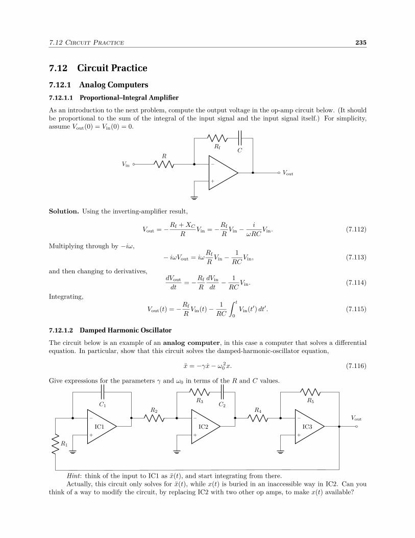
7.12 Circuit Practice 235
7.12 Circuit Practice
7.12.1 Analog Computers
7.12.1.1 Proportional–Integral Amplifier
As an introduction to the next problem, compute the output voltage in the op-amp circuit below. (It shouldbe proportional to the sum of the integral of the input signal and the input signal itself.) For simplicity,assume Vout(0) = Vin(0) = 0.
−
+
Vout
RfC
R
Vin
Solution. Using the inverting-amplifier result,
Vout = −Rf + XC
RVin = −Rf
RVin −
i
ωRCVin. (7.112)
Multiplying through by −iω,
− iωVout = iωRf
RVin −
1
RCVin, (7.113)
and then changing to derivatives,dVout
dt= −Rf
R
dVin
dt− 1
RCVin. (7.114)
Integrating,
Vout(t) = −Rf
RVin(t)− 1
RC
∫ t
0
Vin(t′) dt′. (7.115)
7.12.1.2 Damped Harmonic Oscillator
The circuit below is an example of an analog computer, in this case a computer that solves a differentialequation. In particular, show that this circuit solves the damped-harmonic-oscillator equation,
x = −γx− ω 20 x. (7.116)
Give expressions for the parameters γ and ω0 in terms of the R and C values.
−
+
IC2
−
+
IC3
−
+
IC1
R3C2
R2 R4
R5C1
R1
Vout
Hint: think of the input to IC1 as x(t), and start integrating from there.Actually, this circuit only solves for x(t), while x(t) is buried in an inaccessible way in IC2. Can you
think of a way to modify the circuit, by replacing IC2 with two other op amps, to make x(t) available?

236 Chapter 7. Operational Amplifiers
Note also in particular how R3 controls the damping (γ) for the circuit.
Solution. Suppose the input to the IC1 integrator is x. Then the output of IC1 (and the input of IC2) is
VIC1 = − x
R1C1. (7.117)
Now applying the results of the first problem, the output of IC2 is
VIC2 =R3
R1R2C1x +
x
R1R2C1C2. (7.118)
The last op amp just inverts with some gain:
VIC3 = Vout = − R3R5
R1R2R4C1x− R5
R1R2R4C1C2x. (7.119)
Then Vout = x, so we have the equation
x = − R3R5
R1R2R4C1x− R5
R1R2R4C1C2x. (7.120)
This is the harmonic-oscillator equation with
γ =R3R5
R1R2R4C1, ω0 =
√
R5
R1R2R4C1C2. (7.121)
Note that we set Vout to x, so this solves for the second derivative. To make x(t) available, replace IC2 bytwo op amps, one an integrator and one an inverting amplifier. Then use IC3 as an inverting summer. Thex(t) signal is then available on the output of the inverting amplifier.
7.12.2 Gyrator
The circuit below is an example of a gyrator,13 which presents an effective impedance based on the con-stituent impedances Z1–Z5 (which are not necessarily resistors).
13Paul Horowitz and Winfield Hill, The Art of Electronics, 2nd ed. (Cambridge, 1989), p. 291 (ISBN: 0521370957).

7.12 Circuit Practice 237
Z5
Z4
Z3
Z2
Z1
−
+
−
+
Zeff =Z1Z3Z5
Z2Z4
(a) Show that the effective input impedance is as advertised. Begin by considering a voltage V and acurrent I at the input terminal, and divide them to obtain the impedance.
Hints: to get you started, here are a few things to simplify and keep things organized. First, considercurrents I1–I5, flowing through “resistors” Z1–Z5, all in the direction of the ground connection.
Second, assume that both op amps are operating “normally” with negative feedback (this is plausible
in this circuit, since the outputs are “closer” in the impedance chain to the negative inputs than to thenegative outputs, but strictly speaking this would need to be proven; for simplicity, just assume this is thecase).
Third, note that V = I5Z5. (Why?)Finally, use what you know about op amps to relate all the different currents together; you don’t need
to consider any other currents besides I and I1–I5, and obviously you want to eliminate all of them but I.(b) One of the utilities of this circuit is to realize an effective inductor using only op amps, resistors,
and capacitors. This is useful since these components are often better behaved (i.e., closer to ideal) thaninductors. Suppose Z4 is a capacitor in this circuit, with the rest resistors. Show that the result is aneffective inductor, and give the effective inductance. What set of (reasonable) components would give you a1-H inductor? (A pretty big inductor!)
Solution.(a) We start with
V = I5Z5. (7.122)
This is because the voltage drop across the other four resistors must be zero, because they are wrappedbetween the inputs of the op amps.
Now the voltage between the inputs of the right-hand op amp is zero, so
I3Z3 = −I4Z4. (7.123)
238 Chapter 7. Operational Amplifiers
Then using I4 = I5 (no current into the op-amp input), we find
V = I4Z5 = −Z3Z5
Z4I3. (7.124)
Repeating this argument, we haveI1Z1 = −I2Z2 (7.125)
and I2 = I3, so
V = −Z3Z5
Z4I2 =
Z1Z3Z5
Z2Z4I1. (7.126)
Finally, I1 = I, so
V =Z1Z3Z5
Z2Z4I =: IZeff , (7.127)
which establishes the effective impedance.(b) With
Zeff =Z1Z3Z5
Z2Z4(7.128)
and setting Z4 = i/ωC and the other impedances to resistances,
Zeff = −iωR1R3R5C
R2. (7.129)
Comparing this toXL = −iωL, (7.130)
we have an inductance
Leff =R1R3R5C
R2. (7.131)
With C = 0.01 µF, we could pick all resistors to be 10 kΩ, which would give 1 H of inductance.
7.12.3 Guitar Preamp with Midrange Boost/Cut
The circuit on the next page is a preamplifier for an electric guitar, powered from a single 9-V battery. Itis designed for a Fender Stratocaster, and uses one of the “tone knobs” to control a midrange boost or cut(a midrange boost gives a “fat” sound more like a Les Paul guitar, with “humbucking pickups;” a midrangecut gives a clear, “thin” sound, more like the neck pickup on a Fender Telecaster guitar). The PCB design isalso shown, printed at actual size. (Compare this circuit to the preamplifier for the Eric Clapton SignatureStratocaster from Section 4.16.4.)
Try to work through the circuit and understand each of the elements, noting the following:
• Since this circuit is powered by a single 9-V battery, but the signal is bipolar, all circuits must bereferenced to the “effective ground” of 4.5 V. For example, the input is ac-coupled and biased at thiseffective ground.
• There are four op-amps, but all packaged in one chip. Hence the “1/4 OP462,” and the IC pin numberson each op-amp.
• First, convince yourself that the input op-amp (pins 1-3) is an ac-coupled, unity-gain buffer.
• Now, the upper-left op-amp (pins 5-7) functions as a noninverting amplifier. But the capacitor givesa frequency-dependent gain. You should convince yourself that the dc gain is unity, but the ac gain ishigher. What is the ac gain? Why do we want unity gain at dc?

7.12 Circuit Practice 239
• The upper-right-hand op-amp is less obvious, but this is an inverting bandpass filter, as suggestedby the center frequency and Q factor. Note that the noninverting input is biased at virtual ground(normally this input would just be grounded), and that there are two R–C pairs at the input (R7 inparallel with R8 and R9, with C4; and R12 with C5) that together give the bandpass action, becausethey act something like cascaded low-pass and high-pass filters. (See Problem 7.24.)
• The final op-amp (pins 12-14) combines the filtered signal with the original to give the boost or cut.Capacitor C2 rolls off the gain at high frequencies, where the combination may not be accurate due todifferent delays at the inputs.
• To control the amount of boost or cut, a potentiometer (with color-coded wires according to thestandard Fender convention for the tone knob) interpolates between the buffered input signal and theinverted version produced by the last op-amp.
• The output is ac-coupled and biased to ground.
• Note the diode in the battery/power-supply connection, which protects the op-amp in case the batteryis accidentally connected in reverse. A single bypass capacitor stabilizes all op-amps, since they are ina single package. The op-amp operates at low power, so the bypass capacitor value and location arenot critical; a larger capacitance is fine since the capacitor does not need to work well at very highfrequencies (audio = low frequency in circuits).

240 Chapter 7. Operational Amplifiers
R1
2.2
MΩ
+9V
INP
UT
- +1/
4 O
P46
2
32
1- +
R2
2.2
MΩ
C1
0.1
µF
1/4
OP
462
R14
1.0
MΩ
C6
0.1
µF
OU
TP
UT
250K
lin
ear
tap
er
-+
1/4
OP
462
+9V
1/4
OP
462
- +
R3
71.5
kΩ
R4
71.5
kΩ
C2
33 p
F
R5
100
kΩ
R6
28 kΩ
C3
0.1
µF
C4
0.01
µF
R7
35.7
kΩ
R8
56 kΩ
C5
0.01
µF
R9
56 kΩ
R15
1.0
kΩ
GU
ITA
R P
RE
AM
P/
MID
-BO
OS
T C
IRC
UIT
D. A
. ST
EC
K4/
8/00
20 d
BC
ut
20 d
BB
oo
st
Cen
ter
Fre
qu
ency
= 4
44 H
z M
id-B
and
Gai
n =
-1.
15
Q
= 1
.14
+
1 µ
F1N
914
9V
+9V
1213
14
65
7
109
8
+9V
R10
63.4
kΩ
R11
63.4
kΩR
1282
kΩ
R13
35.7
kΩ
pu
rple
gre
yw
hit
e
blu
e
yel
low
red
bla
ck
1R1
C1
R2
R3
INBST
CTL
R6
R5
C3
R11
R7
R10R1
4
OUT GND
9V
BYPS
MID BOOST/CUT
C2
R4
CUT
R8
R9
R12
C4
C5
R13
C6
R1
5
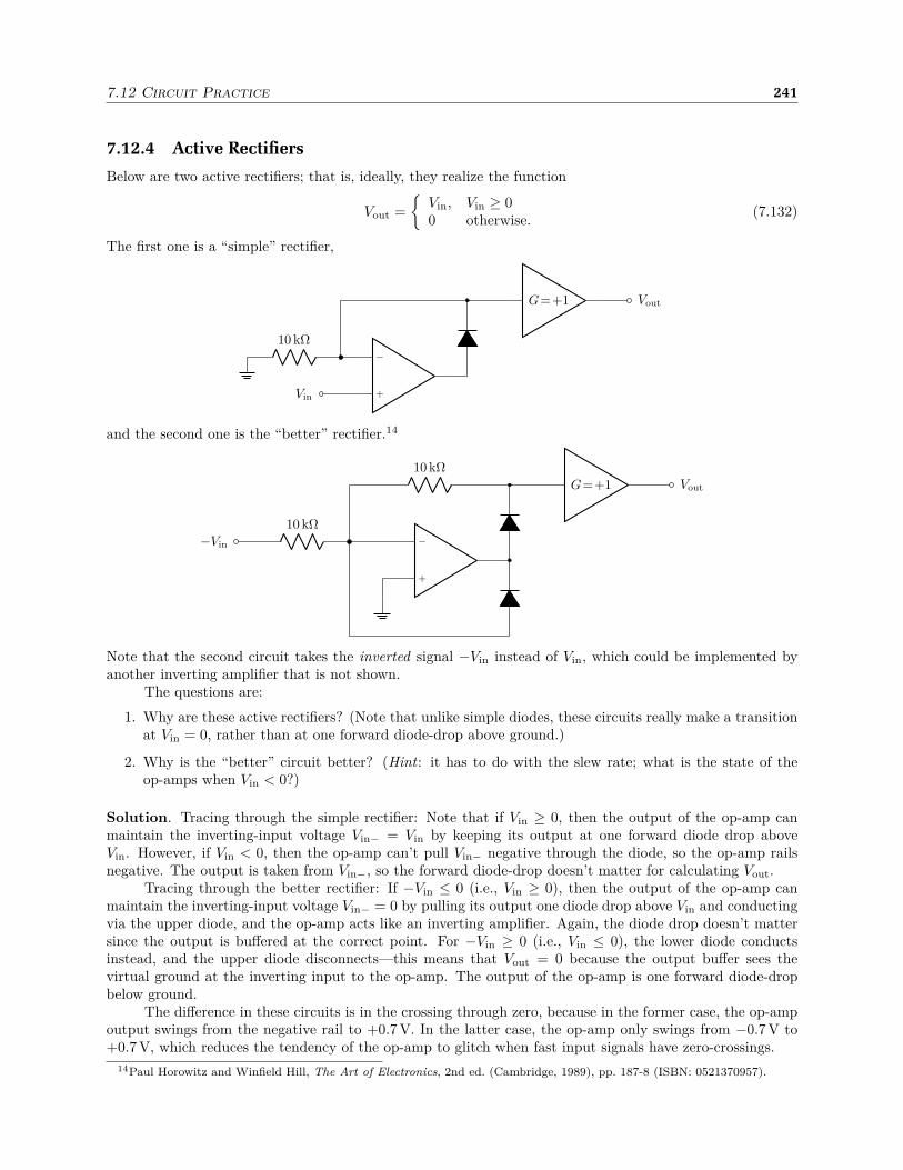
7.12 Circuit Practice 241
7.12.4 Active Rectifiers
Below are two active rectifiers; that is, ideally, they realize the function
Vout =
Vin, Vin ≥ 00 otherwise.
(7.132)
The first one is a “simple” rectifier,
−
+
G=+1
10 kΩ
Vin
Vout
and the second one is the “better” rectifier.14
−
+
G=+1
10 kΩ
10 kΩ
−Vin
Vout
Note that the second circuit takes the inverted signal −Vin instead of Vin, which could be implemented byanother inverting amplifier that is not shown.
The questions are:
1. Why are these active rectifiers? (Note that unlike simple diodes, these circuits really make a transitionat Vin = 0, rather than at one forward diode-drop above ground.)
2. Why is the “better” circuit better? (Hint: it has to do with the slew rate; what is the state of theop-amps when Vin < 0?)
Solution. Tracing through the simple rectifier: Note that if Vin ≥ 0, then the output of the op-amp canmaintain the inverting-input voltage Vin− = Vin by keeping its output at one forward diode drop aboveVin. However, if Vin < 0, then the op-amp can’t pull Vin− negative through the diode, so the op-amp railsnegative. The output is taken from Vin−, so the forward diode-drop doesn’t matter for calculating Vout.
Tracing through the better rectifier: If −Vin ≤ 0 (i.e., Vin ≥ 0), then the output of the op-amp canmaintain the inverting-input voltage Vin− = 0 by pulling its output one diode drop above Vin and conductingvia the upper diode, and the op-amp acts like an inverting amplifier. Again, the diode drop doesn’t mattersince the output is buffered at the correct point. For −Vin ≥ 0 (i.e., Vin ≤ 0), the lower diode conductsinstead, and the upper diode disconnects—this means that Vout = 0 because the output buffer sees thevirtual ground at the inverting input to the op-amp. The output of the op-amp is one forward diode-dropbelow ground.
The difference in these circuits is in the crossing through zero, because in the former case, the op-ampoutput swings from the negative rail to +0.7 V. In the latter case, the op-amp only swings from −0.7 V to+0.7 V, which reduces the tendency of the op-amp to glitch when fast input signals have zero-crossings.
14Paul Horowitz and Winfield Hill, The Art of Electronics, 2nd ed. (Cambridge, 1989), pp. 187-8 (ISBN: 0521370957).
242 Chapter 7. Operational Amplifiers
7.12.5 Pulse-Area Stabilizer
The circuit on the next page is designed for the following purpose. To take photographs with a laser pulse,it it desirable to have the same exposure from each pulse. But the intensity of the laser drifts. Rather thantry to stabilize the intensity of the laser, we can compensate for the drift by changing the duration of eachlaser pulse to compensate. By making the pulse area or integrated energy of each pulse the same, thephotographs have exactly the same exposure, independent of the laser intensity.
Try to trace through the following features in the circuit.
1. The reference IC6 provides a stable voltage to bias the photodiode. What is the voltage at pin 2?
2. You should then convince yourself that the photodiode PD1 is reverse-biased. This helps to improvethe speed of the photodiode. The photodiode itself acts as a current source, with current flowing fromcathode to anode.
3. What kind of op-amp circuit is IC1? How is the output related to the photodiode signal? (Answer:the op-amp output is positive and proportional to the photocurrent.)
4. IC2 is an integrator, with a MOSFET to reset the integrating capacitor.
5. IC3 is a comparator, connected as a Schmitt trigger. It detects when the integral of the laser pulseintensity reaches a set value from input jack J3. Its output drives digital logic circuitry, to which wewill return later after we have studied digital electronics.
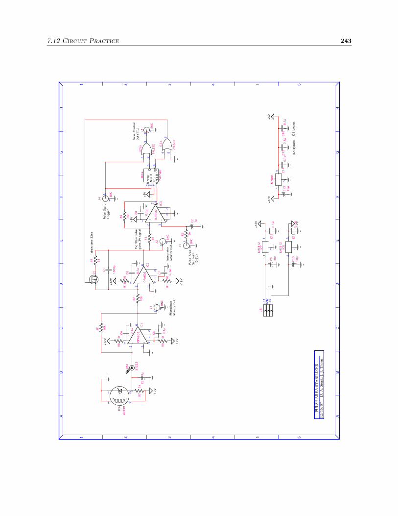
7.12 Circuit Practice 243
A A
B B
C C
D D
E E
F F
G G
H H
11
22
33
44
55
66
PU
LSE
AR
EA
ST
AB
ILIZ
ER
12/
15/
07
D
. A
. Ste
ck,
J. J
. T
ho
rn
IC5
bypass
IC4
bypass
dra
in t
ime 3
3ns
1V
, 3
0µs p
uls
e
giv
es 3
V s
ignal
Puls
e C
ontr
ol
Out
(TTL)
Puls
e Sta
rt
Tri
gg
er
(0-5
V)
Puls
e A
rea
Set
Poin
t
Inte
gra
tor
Monit
or
Out
Photo
dio
de
Monit
or
Out
/P
RE
CLK
D /C
LR
Q
/Q
4 3 2 1
5 6
IC4
a
74F74N
10
k
R1
3
4
J3
BN
C
1000p
C1
3
4
J1
BN
C10
k
R2
3
4
J2
BN
C 10
k
R3
1µ
C2
+5V
3
4
J4
BN
C
3
4
J5
BN
C
Q1
33
R4
1k
R5
1M
R6
+5V
1 23
IC5
a
74
LS3
2
+ -1 2
3 4
LM
39
9
IC6
5k
R7 -1
2V
S1
22
3
PD
1
10
R8
10
R9
10
R1
0
10
R1
1
-12
V
-12
V
+12V
+12V
- +
2 3
4
1
5
7
6O
PA
60
2
IC1
0.1
µ
C5
0.1
µ
C6
0.1
µ
C7
0.1
µ
C8
-+ 4
2 3
1
5
6
78
IC3
TL3
01
6
- +
2 3
4
1
5
7
6O
PA
60
2IC
2
0.1
µ
C4
4 56
IC5
b
74
LS3
2
1µ
C3
12
3IC
7LM
78
12
2
1
3
IC8
LM
79
12
1
2
3IC
9LM
78
05
+1
5GN
D-1
5
J6
+12V
-12
V
+12V
10
µ
C9
10
µ
C1
3
10
µ
C1
0
+5V
0.1
µC1
1
0.1
µC1
2
0.1
µC1
40
.1µ
C1
50
.1µ
C1
6

244 Chapter 7. Operational Amplifiers
7.13 Exercises
Problem 7.1
Consider the following op-amp circuit, which contains one resistor (of resistance R), and one schme-sistor.
−
+
Vout
S
R
Vin
Recall (Problem 1.15) that a “schmesistor” is a device that obeys “Schmohm’s law,”
V = I2S, (7.133)
where S is the “schmesistance.” Derive an expression for Vout in terms of Vin, R, and S.
Problem 7.2
Consider the following op-amp circuit, which contains one resistor (of resistance R), and one “schme-sistor.”
−
+
Vout
R
S
Vin
Recall that a “schmesistor” is a device that obeys “Shmohm’s law,”
V = I2S, (7.134)
where S is the “schmesistance.” Derive an expression for Vout in terms of Vin, R, and S.
Problem 7.3
Show that Vout = V1 + V2 in the circuit below.

7.13 Exercises 245
−
+
Vout = V1 + V2
R
R
R
V1
R
V2
Problem 7.4
(a) Consider the following op-amp circuit, which contains one resistor (of resistance R), and oneschmapacitor (see Problem 2.9) of schmapacitance S.
−
+
Vout
S
R
Vin
Derive an expression for Vout(t) in terms of an arbitrary, time-dependent input Vin(t), R, and S.Assume an ideal op-amp.
Recall that the schmapacitor is defined by the relation
I = Sd3V
dt3, (7.135)
where I is the schmapacitor current and V is the voltage drop across the schmapacitor.
(b) Of course, schmapacitors aren’t real. Describe briefly and qualitatively how you could build anequivalent circuit using real-world components.
Problem 7.5
(a) A photodiode produces a backwards current (i.e., current flows from cathode to anode) whendetecting light. (Think of this as the opposite of an LED, where a forward current causes light to beemitted. In fact, an LED can work as a photodiode, though not a particularly great one.) Consider thephotodiode-amplifier (op-amp) circuit below, which acts as a transimpedance amplifier (currentinput, voltage output). Write down an expression for the output voltage in terms of the photodiodecurrent and R. Is the output voltage positive or negative when you shine light on the photodiode?
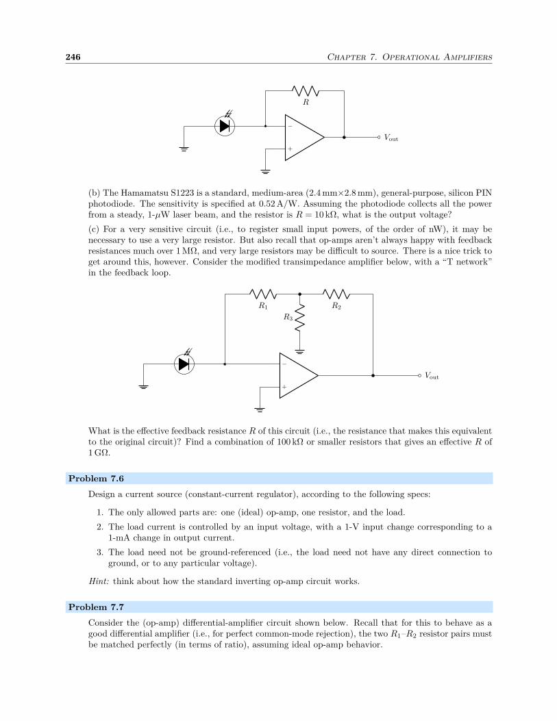
246 Chapter 7. Operational Amplifiers
−
+
Vout
R
(b) The Hamamatsu S1223 is a standard, medium-area (2.4 mm×2.8 mm), general-purpose, silicon PINphotodiode. The sensitivity is specified at 0.52 A/W. Assuming the photodiode collects all the powerfrom a steady, 1-µW laser beam, and the resistor is R = 10 kΩ, what is the output voltage?
(c) For a very sensitive circuit (i.e., to register small input powers, of the order of nW), it may benecessary to use a very large resistor. But also recall that op-amps aren’t always happy with feedbackresistances much over 1 MΩ, and very large resistors may be difficult to source. There is a nice trick toget around this, however. Consider the modified transimpedance amplifier below, with a “T network”in the feedback loop.
−
+
Vout
R2R1
R3
What is the effective feedback resistance R of this circuit (i.e., the resistance that makes this equivalentto the original circuit)? Find a combination of 100 kΩ or smaller resistors that gives an effective R of1 GΩ.
Problem 7.6
Design a current source (constant-current regulator), according to the following specs:
1. The only allowed parts are: one (ideal) op-amp, one resistor, and the load.
2. The load current is controlled by an input voltage, with a 1-V input change corresponding to a1-mA change in output current.
3. The load need not be ground-referenced (i.e., the load need not have any direct connection toground, or to any particular voltage).
Hint: think about how the standard inverting op-amp circuit works.
Problem 7.7
Consider the (op-amp) differential-amplifier circuit shown below. Recall that for this to behave as agood differential amplifier (i.e., for perfect common-mode rejection), the two R1–R2 resistor pairs mustbe matched perfectly (in terms of ratio), assuming ideal op-amp behavior.
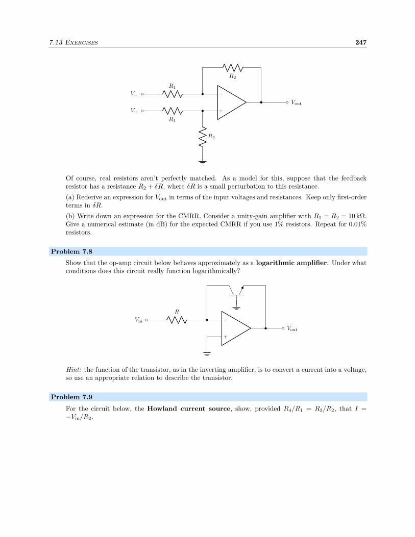
7.13 Exercises 247
−
+
Vout
R2
R2
R1
V−
R1
V+
Of course, real resistors aren’t perfectly matched. As a model for this, suppose that the feedbackresistor has a resistance R2 + δR, where δR is a small perturbation to this resistance.
(a) Rederive an expression for Vout in terms of the input voltages and resistances. Keep only first-orderterms in δR.
(b) Write down an expression for the CMRR. Consider a unity-gain amplifier with R1 = R2 = 10 kΩ.Give a numerical estimate (in dB) for the expected CMRR if you use 1% resistors. Repeat for 0.01%resistors.
Problem 7.8
Show that the op-amp circuit below behaves approximately as a logarithmic amplifier. Under whatconditions does this circuit really function logarithmically?
−
+
Vout
R
Vin
Hint: the function of the transistor, as in the inverting amplifier, is to convert a current into a voltage,so use an appropriate relation to describe the transistor.
Problem 7.9
For the circuit below, the Howland current source, show, provided R4/R1 = R3/R2, that I =−Vin/R2.
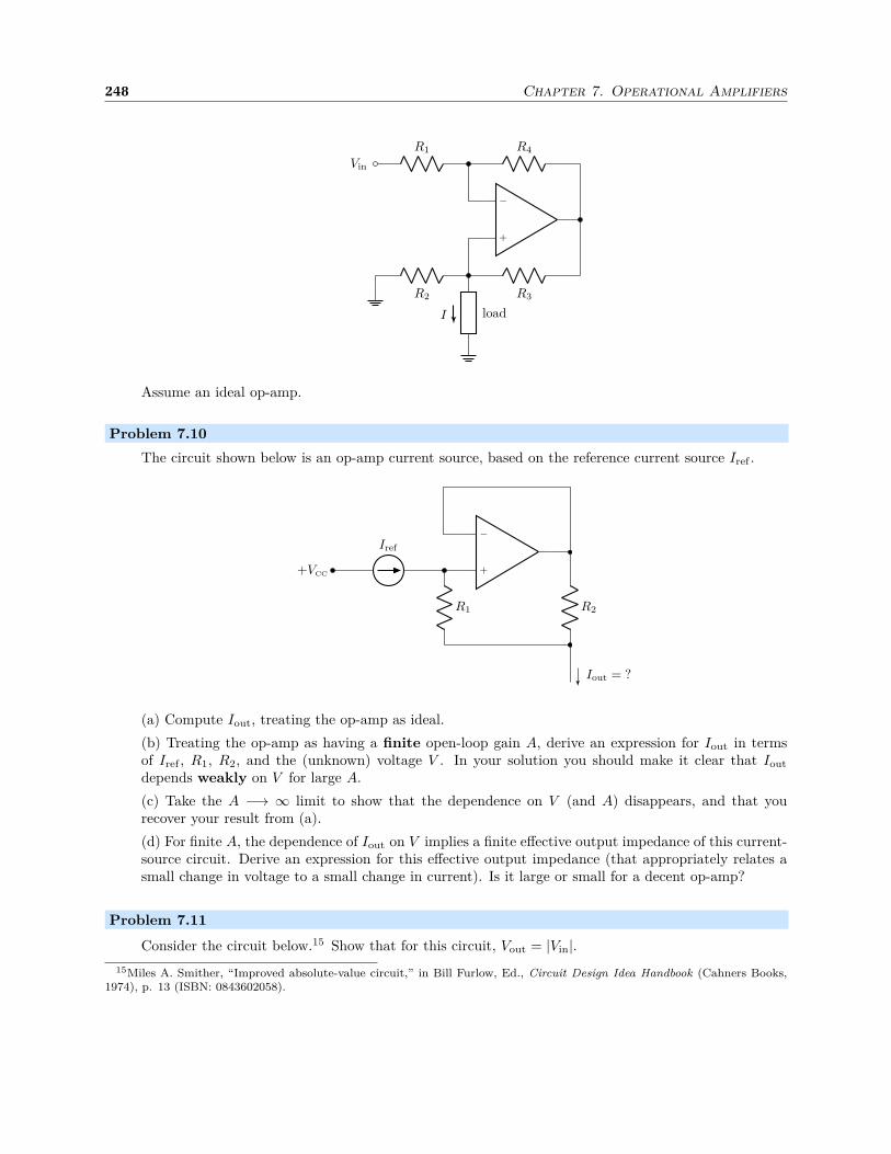
248 Chapter 7. Operational Amplifiers
−
+
R4R1
Vin
R3R2
loadI
Assume an ideal op-amp.
Problem 7.10
The circuit shown below is an op-amp current source, based on the reference current source Iref .
Iout = ?
−
+
R2R1
Iref
+VCC
(a) Compute Iout, treating the op-amp as ideal.
(b) Treating the op-amp as having a finite open-loop gain A, derive an expression for Iout in termsof Iref , R1, R2, and the (unknown) voltage V . In your solution you should make it clear that Iout
depends weakly on V for large A.
(c) Take the A −→ ∞ limit to show that the dependence on V (and A) disappears, and that yourecover your result from (a).
(d) For finite A, the dependence of Iout on V implies a finite effective output impedance of this current-source circuit. Derive an expression for this effective output impedance (that appropriately relates asmall change in voltage to a small change in current). Is it large or small for a decent op-amp?
Problem 7.11
Consider the circuit below.15 Show that for this circuit, Vout = |Vin|.15Miles A. Smither, “Improved absolute-value circuit,” in Bill Furlow, Ed., Circuit Design Idea Handbook (Cahners Books,
1974), p. 13 (ISBN: 0843602058).

7.13 Exercises 249
−
+
IC1
D1
D2
R3 (10k)R4 (10k)
Vin
R6 (10k)
R5 (4.7k)
R2 (10k)
−
+
IC2
R0 (20k)
Vout
R7 (68k)
R1 (20k)
V1
V2
V3
This circuit looks a little complicated, so here is some guidance. Note that you should be able to dothis with very little math, provided you break the circuit down into manageable parts that you havealready learned about.
(a) The IC2 op amp is connected in one of the basic op-amp circuits; what is it?
(b) Now the tricky part is understanding the diode network in the IC1 circuit. Begin by treating D1and D2 as ideal diodes (i.e., no forward voltage drop). Now you should see that only one diode conductsat a time, and in either case IC1 is connected as one of the basic op-amp circuits (which one?). Workout the voltages V1, V2, and V3, and handle separately the cases where the output of IC1 is positive ornegative.
(c) Finally, consider the original circuit with real diodes, and argue that the forward voltage dropsdon’t matter.
Problem 7.12
The purpose of this problem is to show that, in the circuit below, that Vout = maxV1, V2 (i.e., itselects the larger of the input voltages). The diodes here are real diodes (i.e., you must account properlyfor any voltage drops across the diodes), and there are no restrictions on the signs of the input voltages.
−
+
R2
R2
R1
V1
R1
V2
D1
D2
R1 −
+Vout = maxV1, V2
V3
Vo
I
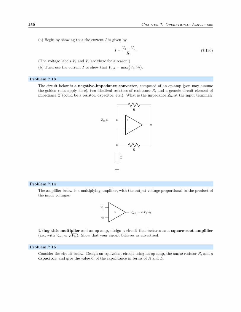
250 Chapter 7. Operational Amplifiers
(a) Begin by showing that the current I is given by
I =V2 − V1
R1. (7.136)
(The voltage labels V3 and Vo are there for a reason!)
(b) Then use the current I to show that Vout = maxV1, V2.
Problem 7.13
The circuit below is a negative-impedance converter, composed of an op-amp (you may assumethe golden rules apply here), two identical resistors of resistance R, and a generic circuit element ofimpedance Z (could be a resistor, capacitor, etc.). What is the impedance Zin at the input terminal?
−
+
R
R
Z
Zin
Problem 7.14
The amplifier below is a multiplying amplifier, with the output voltage proportional to the product ofthe input voltages.
×V1
V2
Vout = αV1V2
Using this multiplier and an op-amp, design a circuit that behaves as a square-root amplifier(i.e., with Vout ∝
√Vin). Show that your circuit behaves as advertised.
Problem 7.15
Consider the circuit below. Design an equivalent circuit using an op-amp, the same resistor R, and acapacitor, and give the value C of the capacitance in terms of R and L.
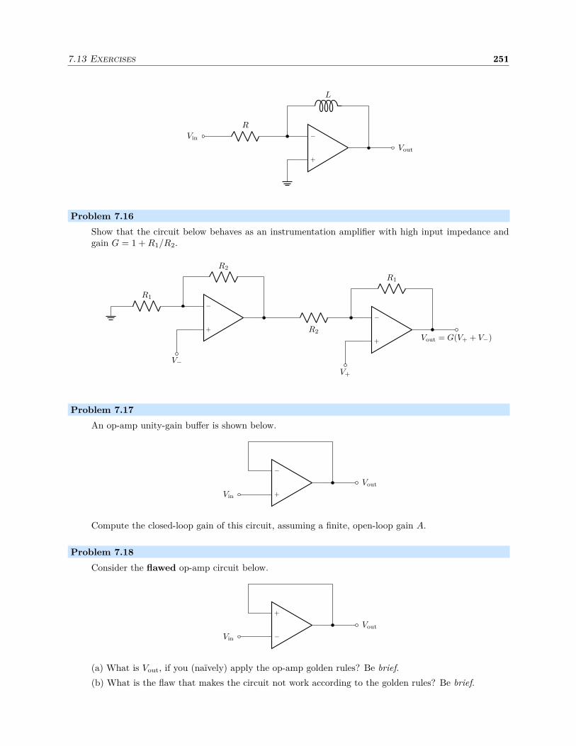
7.13 Exercises 251
−
+
Vout
L
R
Vin
Problem 7.16
Show that the circuit below behaves as an instrumentation amplifier with high input impedance andgain G = 1 + R1/R2.
−
+
R2
R1
V−
−
+
R2
V+
R1
Vout = G(V+ + V−)
Problem 7.17
An op-amp unity-gain buffer is shown below.
−
+
Vout
Vin
Compute the closed-loop gain of this circuit, assuming a finite, open-loop gain A.
Problem 7.18
Consider the flawed op-amp circuit below.
−
+
Vout
Vin
(a) What is Vout, if you (naïvely) apply the op-amp golden rules? Be brief.
(b) What is the flaw that makes the circuit not work according to the golden rules? Be brief.

252 Chapter 7. Operational Amplifiers
(c) Show mathematically that the circuit doesn’t work according to the golden-rule solution. [Use theop-amp relation Vout = A(Vin+ − Vin−), where A is the open-loop gain, and consider what the op-amp“wants” to do in the presence of a small output error ǫ.] What does the op-amp do instead?
(d) Go through the stability analysis of part (c) again, but take the error to be added to the finite-Asolution for Vout. Explain any difference you find in your solution here from that of part (c).
Problem 7.19
Consider the transimpedance amplifier below. The op amp has finite open-loop gain A.
−
+
R
I
Vout
(a) Derive an expression for Vout in terms of the input current I. Also take the limit as A −→∞.
(b) Derive an expression for the input impedance of the circuit. Ignore any intrinsic input impedanceRi of the op-amp inputs.
(c) Derive an expression for the output impedance of the circuit.
Problem 7.20
Consider the transimpedance amplifier below with input capacitance C. This circuit acts as a modelfor instability in a photodiode amplifier, where recall that a photodiode acts as a current source, andC models the photodiode capacitance.
−
+
R
I
VoutC
(a) Derive an expression for the frequency-dependent transimpedance Z(ω) of the amplifier [i.e., suchthat Vout = IZ(ω) for an input current of frequency ω], assuming a finite open-loop op-amp gain A.Also take the limit as A −→∞.
(b) Show that, if the open-loop gain falls off like a low-pass filter, A(ω) = A0/(1 − iω/ω0), that themagnitude of Z(ω) is peaked at some frequency ω > 0 if A0 is sufficiently large.
(c) Find the peak frequency.
Problem 7.21
Derive an expression for Vout in the circuit below, in the regime where the output is not railed (assumethat R is of the order of 10 kΩ). Also, you may assume Vin ≥ 0 (but assume Vin is not so large thatit damages the transistor) and an ideal op amp. Finally, the op amp is powered from ±VCC. Be clearabout any assumptions you make.

7.13 Exercises 253
−
+
R
Vout
Vin
R/2
+VCC
Problem 7.22
In the circuit below, derive an expression for Vout, assuming an ideal op amp.
−
+
V
R
RVR
Vin
R R
Vout
Problem 7.23
In the circuit below, the diamond-shaped arrangement of resistors is called a Wheatstone bridge,and can act as a sensitive measure of the mismatch of two resistors (here R and R+δR). This is useful,for example, in sensing the value of a thermistor (semiconductor resistor whose resistance varies withtemperature).
−
+
R + δRR
R0 R0
+V
Rf
Rf
Vout
For this circuit, derive an expression for Vout. To keep the algebra under control, give the answer onlyto lowest order in the small perturbation δR [i.e., give the lowest-order term in the Taylor expansionabout δR = 0; you will need to use (a + δa)−1 ≈ a−1 − δa/a2 for δa≪ a].

254 Chapter 7. Operational Amplifiers
Problem 7.24
Consider the following circuit, an active, inverting, band-pass filter. (This is the bandpass filter fromthe guitar preamplifier in Section 7.12.3.)
−
+
Vout
R3C2
C1R1
Vin
R2
(a) Derive an expression for the gain function G(ω), and the amplitude gain function G(ω). Notethat these are the same as the transfer function and amplitude transfer function, respectively, in thepassive-filter case.
Note: an algebra program like Mathematica will make this problem considerably simpler. Contact meif you need help with learning how to use it for algebra or making plots.
(b) Derive asymptotic expressions for G(ω) for large and small frequencies. From these expressions,argue that this is a band-pass filter.
(c) Find an expression for the center frequency, where G(ω) is maximum. Give a numerical valuefor this frequency (give the frequency in Hz, not rad/s), for the component values R1 = 35.7 kΩ,R2 = 28 kΩ, R3 = 82 kΩ, C1 = C2 = 0.01 µF.
(d) Find an expression for the peak gain, i.e., the value of G(ω) at the frequency you derived in part(c). Again, give a numerical value for the same component values.
(e) Make a log-log plot of G(ω), over a reasonable range of frequencies, for the component values above.(Keep in mind this is intended as an audio band-pass filter.)
Problem 7.25
Consider the circuit below, which is intended as a voltage-controlled current source.16 Assume the“output voltage” Vout is held to a fixed voltage by an external source.
−
+
−
+
1 kΩ
1 kΩ
1 kΩ
Vout
1 kΩ
2 kΩ
Vin
1 kΩ
1 µF
1 kΩ
1 kΩ
IC1
IC2
Iout
16This is the modulation input stage of the current-controller circuit in K. G. Libbrecht and J. L. Hall, “A low-noise high-speeddiode laser current controller,” Reviews of Scientific Instruments 64, 2133 (1993).
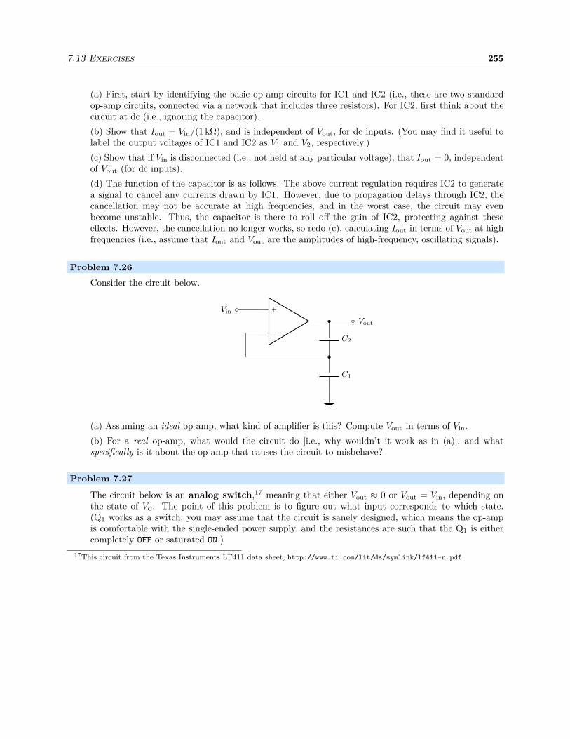
7.13 Exercises 255
(a) First, start by identifying the basic op-amp circuits for IC1 and IC2 (i.e., these are two standardop-amp circuits, connected via a network that includes three resistors). For IC2, first think about thecircuit at dc (i.e., ignoring the capacitor).
(b) Show that Iout = Vin/(1 kΩ), and is independent of Vout, for dc inputs. (You may find it useful tolabel the output voltages of IC1 and IC2 as V1 and V2, respectively.)
(c) Show that if Vin is disconnected (i.e., not held at any particular voltage), that Iout = 0, independentof Vout (for dc inputs).
(d) The function of the capacitor is as follows. The above current regulation requires IC2 to generatea signal to cancel any currents drawn by IC1. However, due to propagation delays through IC2, thecancellation may not be accurate at high frequencies, and in the worst case, the circuit may evenbecome unstable. Thus, the capacitor is there to roll off the gain of IC2, protecting against theseeffects. However, the cancellation no longer works, so redo (c), calculating Iout in terms of Vout at highfrequencies (i.e., assume that Iout and Vout are the amplitudes of high-frequency, oscillating signals).
Problem 7.26
Consider the circuit below.
−
+
Vout
C2
C1
Vin
(a) Assuming an ideal op-amp, what kind of amplifier is this? Compute Vout in terms of Vin.
(b) For a real op-amp, what would the circuit do [i.e., why wouldn’t it work as in (a)], and whatspecifically is it about the op-amp that causes the circuit to misbehave?
Problem 7.27
The circuit below is an analog switch,17 meaning that either Vout ≈ 0 or Vout = Vin, depending onthe state of VC. The point of this problem is to figure out what input corresponds to which state.(Q1 works as a switch; you may assume that the circuit is sanely designed, which means the op-ampis comfortable with the single-ended power supply, and the resistances are such that the Q1 is eithercompletely OFF or saturated ON.)
17This circuit from the Texas Instruments LF411 data sheet, http://www.ti.com/lit/ds/symlink/lf411-n.pdf.
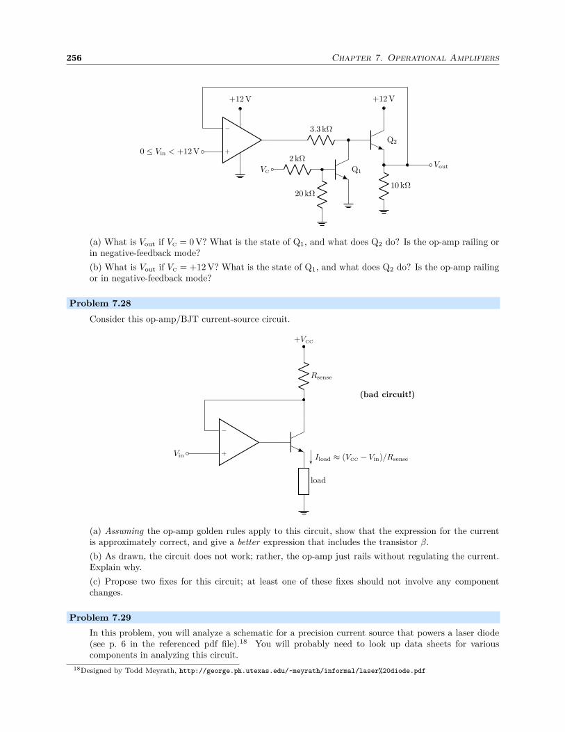
256 Chapter 7. Operational Amplifiers
−
+
Q2
Q1
3.3 kΩ
+12 V
0 ≤ Vin < +12 V
Vout
+12 V
10 kΩ20 kΩ
2 kΩ
VC
(a) What is Vout if VC = 0 V? What is the state of Q1, and what does Q2 do? Is the op-amp railing orin negative-feedback mode?
(b) What is Vout if VC = +12 V? What is the state of Q1, and what does Q2 do? Is the op-amp railingor in negative-feedback mode?
Problem 7.28
Consider this op-amp/BJT current-source circuit.
−
+
Rsense
+VCC
Vin
load
Iload ≈ (VCC − Vin)/Rsense
(bad circuit!)
(a) Assuming the op-amp golden rules apply to this circuit, show that the expression for the currentis approximately correct, and give a better expression that includes the transistor β.
(b) As drawn, the circuit does not work; rather, the op-amp just rails without regulating the current.Explain why.
(c) Propose two fixes for this circuit; at least one of these fixes should not involve any componentchanges.
Problem 7.29
In this problem, you will analyze a schematic for a precision current source that powers a laser diode(see p. 6 in the referenced pdf file).18 You will probably need to look up data sheets for variouscomponents in analyzing this circuit.
18Designed by Todd Meyrath, http://george.ph.utexas.edu/~meyrath/informal/laser%20diode.pdf

7.13 Exercises 257
(a) Suppose Rlimit = 10 kΩ. What is the maximum possible (dc) voltage at pin 3 of the AD820?Assume the 2N7000 is an open circuit. This is the control voltage that sets the current through thelaser diode. Note that the 20-kΩ wiper of the (course adjust) pot is bypassed by a capacitor to ensurethe control voltage has little high-frequency noise.
(b) Now look at the relay on the left-hand side of the schematic. This is the “laser enable” partof the circuit, which either passes or overrides (i.e., sets to zero) the control voltage. Note the twomomentary switches (i.e., they are push-buttons, only connected while you are actually pushing thembut the circuit “remembers” the last one you pushed). Explain how this section of the circuit worksto enable and disable the laser. Include the operation of the status LED (why doesn’t the LED burnout if it is powered by 15 V?), and explain why this circuit has a “soft-start” feature.
(c) Now analyze the AD820, which regulates the diode current according to the control voltage at pin3. For the purposes of this analysis, ignore C0, C1, and R1 (i.e., replace them by open connections)as well as R0, R2, and C2 (i.e., replace them by short circuits). These are needed for stability, butI haven’t discussed much about this yet. Thus, the feedback loop consists of the BUF634’s, resistorSR10, and the INA128 (assume the gain of the INA128 is 10). What is the purpose of the BUF634’s,why are there 2 of them, and what is with the 10 Ω resistors? What is the maximum current throughthe laser diode given your answer in (a)? Explain.
(d) Look at the power-supply connections of the various amplifiers. Explain the differences in thebypass circuits, and why the chips are bypassed in different ways (i.e., why not bypass them all in thesame way?).
(e) Now go back to the AD820, and consider it separately from the other ICs, but this time with R0-R2,and C0-C2. Also assume pin 3 is grounded. What is the gain at low frequencies? High frequencies?
Problem 7.30
Consider the op-amp current source shown below.
−
+
Rsense
+VSS
Vin
load
Iload = (VSS − Vin)/Rsense
(a) Show that
Iload =VSS − Vin
Rsense, (7.137)
as advertised.
(b) Note that the MOSFET is a p-channel device. Explain why an n-channel device doesn’t work here(consider how the output changes as Iload increases).

258 Chapter 7. Operational Amplifiers
(c) To analyze the stability issues in this circuit, consider the modified circuit below, with output resistorR (modeling the intrinsic output resistance of the op-amp), and capacitor C. The capacitor modelsthe gate-source capacitance of the FET; for simplicity we are excluding the gate-drain capacitance,although it could be much more important due to the Miller effect, but this extra capacitance couldbe modeled in the following analysis with another capacitor (though some details of the load wouldhave to be included in the analysis).
−
+
RC
Rsense
+VSS
Vin
load
Iload = (VSS − Vin)/Rsense
Consider a small ac signal vin at frequency ω at the input (and some dc bias V0, so Vin = V0 + vin).Treat the FET via its transconductance gm (i.e., iSD = −gmvGS) and the op-amp via the finite-gainformula (7.39)
Vout = A(Vin+ − Vin−), (7.138)
with response
A(ω) =A0
1− iω/ωc, (7.139)
where ωc is the cutoff frequency. Show that the ac load response iload to vin can be written
iload =−gmA0
(1− iωRC)(1− iω/ωc) + gm(1 + A0 − iω/ωc)Rsensevin. (7.140)
(d) Note that the expression above can change sign, which we will see can lead to instability. Intuitively,the op-amp output is inductive, forming a destabilizing resonance with the capacitive gate input of theFET. Show that the circuit exhibits resonance behavior by finding the extreme value of |iload|, as wellas the frequency at which the extremum occurs. Discuss the dependence of the peak frequency on theFET parameters gm and C (simplify your analysis by working in the regime A0 ≫ 1 and ωc ≪ 1/RC).Also simplify your notation by defining the frequency ω0 by
ω 20 :=
ωc
RC. (7.141)
(e) To more precisely consider stability problems in this circuit, we must consider the voltage feedback.To do this we should consider the voltage vS at the inverting input, given by
vS = −iloadRsense =: G(ω) vin, (7.142)
to be the circuit “output,” which then defines the voltage gain G of the circuit. Since this is fed backto the inverting input, G should be positive and preferably large. The problem comes when Re[G] is
7.13 Exercises 259
negative, because it means the feedback is positive. In particular, the circuit becomes unstable whenRe[G(ω)] < −1, because perturbations at any frequency satisfying this condition will grow. Find theextreme value of Re[G] and show that Re[G] < −1 when
A0ωcRC√gmRsense(
√4A0ωcRC +
√gmRsense)
> 1, (7.143)
again in the limits A0 ≫ 1 and ωc ≪ 1/RC. Using typical parameters for a high-speed op-amp anda power MOSFET (ωc/2π = 100 Hz, R = 50 Ω, Rsense = 50 Ω, gm = 1, A0 = 5 × 10⁶) solve theequation to find the range of gate–source capacitance that destabilizes the circuit. Since typical gatecapacitances are on the order of 100 pF, you should find that the circuit is unstable (i.e., it oscillates).More components in the feedback loop are necessary to stabilize it.
Again, to keep your calculations organized, you should use the following definitions to simplify yourcalculation:
G0 := gmRsenseA0ω 20
ω1 := ω0
√
1 + gmRsense(1 + A0)
γ1 :=ω 2
c + (1 + gmRsense) ω 20
ωc.
(7.144)

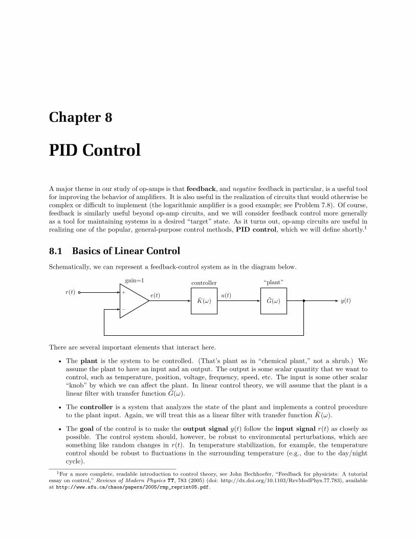
Chapter 8
PID Control
A major theme in our study of op-amps is that feedback, and negative feedback in particular, is a useful toolfor improving the behavior of amplifiers. It is also useful in the realization of circuits that would otherwise becomplex or difficult to implement (the logarithmic amplifier is a good example; see Problem 7.8). Of course,feedback is similarly useful beyond op-amp circuits, and we will consider feedback control more generallyas a tool for maintaining systems in a desired “target” state. As it turns out, op-amp circuits are useful inrealizing one of the popular, general-purpose control methods, PID control, which we will define shortly.1
8.1 Basics of Linear Control
Schematically, we can represent a feedback-control system as in the diagram below.
−
+
K(ω) G(ω)
controller “plant”gain=1
e(t) u(t)y(t)
r(t)
There are several important elements that interact here.
• The plant is the system to be controlled. (That’s plant as in “chemical plant,” not a shrub.) Weassume the plant to have an input and an output. The output is some scalar quantity that we want tocontrol, such as temperature, position, voltage, frequency, speed, etc. The input is some other scalar“knob” by which we can affect the plant. In linear control theory, we will assume that the plant is alinear filter with transfer function G(ω).
• The controller is a system that analyzes the state of the plant and implements a control procedureto the plant input. Again, we will treat this as a linear filter with transfer function K(ω).
• The goal of the control is to make the output signal y(t) follow the input signal r(t) as closely aspossible. The control system should, however, be robust to environmental perturbations, which aresomething like random changes in r(t). In temperature stabilization, for example, the temperaturecontrol should be robust to fluctuations in the surrounding temperature (e.g., due to the day/nightcycle).
1For a more complete, readable introduction to control theory, see John Bechhoefer, “Feedback for physicists: A tutorialessay on control,” Reviews of Modern Physics 77, 783 (2005) (doi: http://dx.doi.org/10.1103/RevModPhys.77.783), availableat http://www.sfu.ca/chaos/papers/2005/rmp_reprint05.pdf.

262 Chapter 8. PID Control
• The error is defined as the difference between the desired and actual states:
e(t) := r(t)− y(t). (8.1)
Because of the negative sign on y(t) here, feeding this error signal into the controller amounts tonegative feedback to the plant, assuming the low-frequency transfer characteristics of the controllerand plant have no phase shift.
• The feedback signal u(t) is the error e(t), modified by the controller in frequency space.
Of course, more realistic systems may not be linear, and may have vector inputs and outputs. Thescalar case is still important both conceptually and practically, so we will focus on only this here; however,note that the vector case can sometimes be treated well enough as several, parallel scalar loops—the natureof feedback control is to correct for errors, and so it can often tolerate some slop in the model. The nonlinearcase is more complex in theory, but often a simple, pragmatic approach is to approximate the nonlinearsystem by a linearized verison, so that linear theory applies. Again, this can sometimes work even when theapproximation is quite drastic.
8.2 Example: First-Order Plant, Proportional Control
As a simple example, suppose we take the plant to be a first-order, low-pass filter, with
G(ω) =G0
1− iω/ω0, (8.2)
where G0 is the dc gain, and ω0 is the cutoff frequency of the filter. A more concrete example where thismodel applies is temperature control of a room, where the input is a simple, electric heater, and the outputis the room temperature. The low-pass-filter nature of the room is apparent in the exponential settling ofthe room temperature when the input (power setting of the heater, not a thermostat) changes.
For the controller we will implement simple proportional control, which just means that the controlsignal is proportional to the error. That is, we have a constant transfer function
K(ω) = KP,(8.3)
(proportional controller transfer function)
where KP is the proportional gain.
8.2.1 General Result: Closed-Loop Transfer Function
To analyze our simple example, we will first examine a more generally useful result. To introduce somenotation, for time domain quantities like y(t), we will denote their frequency-domain counterparts by y(ω)—that is y(ω) is the amplitude of the frequency ω that is present in y(t). Given the connections in the circuitabove, we have
y(ω) = K(ω) G(ω) e(ω), (8.4)
wheree(ω) = r(ω)− y(ω). (8.5)
Eliminating the error e, we havey(ω) = K(ω) G(ω)
[
r(ω)− y(ω)]
. (8.6)
Theny(ω)
[
1 + K(ω) G(ω)]
= K(ω) G(ω) r(ω), (8.7)
so
y(ω) =K(ω) G(ω)
1 + K(ω) G(ω)r(ω). (8.8)

8.2 Example: First-Order Plant, Proportional Control 263
This gives the output response y in terms of the input r. Since the control system is linear, we have derivedthe transfer function for the entire control system, or the closed-loop transfer function
T (ω) =K(ω) G(ω)
1 + K(ω) G(ω).
(8.9)(closed-loop transfer function)
Relating this back to op-amps, in the limit where the gain product KG becomes large, the transfer functionapproaches unity (and is otherwise less than unity).
8.2.2 Frequency-Domain Solution
Returning to our example, we have K = KP and G defined by Eq. (8.2), so the closed-loop transfer functionbecomes
T (ω) =KP G0
KP G0 + 1− iω/ω0. =
(
KP G0
KP G0 + 1
)
1
1− iω/ω0(KP G0 + 1). (8.10)
This is still the transfer function for a low-pass filter, but now the dc gain is
T (ω = 0) =KP G0
KP G0 + 1, (8.11)
compared to the original dc gain of G0, and the control becomes ideal as KP −→∞ (at least in this simplemodel; this is not true in general for real control systems). Also, the new cutoff frequency is ω0(KPG0 + 1),which is larger than the original ω0, particularly for large KP. Since the cutoff frequency is inverselyproportional to the decay time, we can see that a larger cutoff frequency is desirable, as it means the controlsystem “settles” more quickly.
8.2.3 Time-Domain Solution
To examine this settling behavior more, we can also transfer the analysis for this example into the timedomain. Returning to Eq. (8.6), and putting in Eq. (8.2),
y(ω) = K(ω) G(ω)[
r(ω)− y(ω)]
=KP G0
1− iω/ω0
[
r(ω)− y(ω)]
. (8.12)
Rearranging a bit, we findy(ω) (ω0 − iω) = ω0KPG0
[
r(ω)− y(ω)]
. (8.13)
We can change this to the time domain by identifying the time-domain counterparts to each variable, andusing ∂/∂t ≡ −iω, to find
ω0y(t) + y(t) = ω0KPG0
[
r(t)− y(t)]
. (8.14)
Solving for y,y = −ω0y + ω0KPG0(r − y). (8.15)
There are two terms here. The first is a simple damping term, again with a time constant of 1/ω0. Thesecond term is a forcing term, where the system is “driven” by the error e = r− y. The system always triesto eliminate the error. Since it does so via simple exponential relaxation, it is always stable—it never “runsaway” from the zero-error point. Note that the drive is stronger for larger KP, meaning that more controlhas more effect on the system, as we should expect.
8.2.4 Constant Input and Proportional Droop
As a simpler version of this example, let’s try a constant input r(t) = r. What is the steady-state solution(y = 0)? From Eq. (8.15), we have
ω0yss = ω0KPG0(r − yss), (8.16)

264 Chapter 8. PID Control
and solving for the steady-state output yss, we find
yss =KPG0
1 + ω0KPG0r. (8.17)
Then we see that the (proportional) control system only achieves the goal perfectly (eventually) in the limitKP −→ ∞. This is the fundamental problem with proportional control: the controller only acts if there iserror, so there must be some steady-state error, or droop, for any finite proportional gain KP.2 In op-ampcircuits, the gain is large for just this reason, but for more complex, real-world control systems (electronic,mechanical, etc.), there are usually limits on KP to maintain loop stability.
8.3 Integral Control
One approach to fixing the problem is to introduce an infinite gain only at dc, where the time delays thatusually cause feedback-loop stability problems won’t matter much. This is precisely what an integrator does:recall that an op-amp integrator (Section 7.4.2) has a gain of the form −i/ωRC. More generally, integralcontrol has a transfer function of the form
K(ω) =iKI
ωτ,
(8.18)(integral controller transfer function)
where τ is a time constant and KI is the (dimensionless) integral gain (note that τ just acts like anothergain parameter here). Then noting that 1/(−iω) is an antiderivative, the controller output is
u(t) =KI
τ
∫ t
0
dt′ e(t′). (8.19)
That is, the controller has a built-in “memory” of past error in the feedback. This allows correction of thedroop, because we no longer require an error at the present moment to have a nonzero control signal u(t).
8.3.1 Example: First-Order Plant, Integral Control
Now back to the example that we introduced in Section 8.2. In the time domain, the same steps leading upto (8.15) now give
y = −y
τ+
KPG0
τ2
∫ t
0
dt′[
r − y(t′)]
, (8.20)
where we are taking τ = 1/ω0 and we are still assuming a constant control input r. It is more convenient tohandle an ordinary differential equation, rather than an integro-differential equation, so we can differentiatethis equation to obtain
y = − y
τ+
KPG0
τ2
[
r − y(t)]
. (8.21)
In steady state, y = y = 0, and so we haveyss = r, (8.22)
which means that we obtain exactly the target in steady state: there is no droop with (ideal) integral control.
8.3.2 Frequency Domain
In the frequency domain, for this example with general closed-loop transfer function (8.9) and example plantfunction (8.2), we have
T (ω) =K(ω) G(ω)
1 + K(ω) G(ω)=
1
1− iω/ω0KI − ω2/ω 20 KI
. (8.23)
2For a good story of proportional droop, see the introduction to David Sellars, “An Overview of Proportional plus Integral plusDerivative Control and Suggestions for Its Successful Application and Implementation,” http://hdl.handle.net/1969.1/5215.

8.4 Proportional–Integral (PI) Control 265
This transfer function is second order in the denominator because of the frequency dependence of the in-tegrator, and is qualitatively different than the first-order low-pass filter that we obtained for proportionalcontrol.
To see this, compare this to a damped, forced harmonic oscillator, which has the form
y + γy + ω 20 y = f(t), (8.24)
where γ is a damping rate, and f(t) is a forcing function (we have set the mass to 1). In the frequencydomain, this becomes
(
− ω2 − iγω + ω 20
)
y = f(ω), (8.25)
and solving for y gives
y =f(ω)/ω 2
0
1− iγω/ω 20 − ω2/ω 2
0
. (8.26)
The transfer function here has the same form as for the integrator control of a low-pass filter in Eq. (8.23).In the integrator control problem, a large integral gain KI is equivalent to a large oscillation frequency ω0
relative to the damping rate γ in the harmonic-oscillator problem. This leads to underdamped oscillations,which means the controller is overshooting the target state.
Again, note that T (ω) −→ 1 as ω −→ 0. This means that there is no steady-state droop in thisintegral-control example.
8.4 Proportional–Integral (PI) Control
It is, of course, possible to combine the benefits of proportional and integral control by using a controllerwith both features. The simplest way to combine these is a simple linear combination:
K(ω) = KP +iKI
ωτ.
(8.27)(PI-controller transfer function)
This is the transfer function for proportional–integral (PI) control. The second term gives integralcontrol, which eliminates droop issues. The first term is a proportional term, which gives more high-frequency response, and thus faster setting. In the example of the single-pole plant from Section 8.2, if wework out the closed-loop transfer function, we obtain
T (ω) =1− i(KP/KI)(ω/ω0)
1− i(1 + KP)ω/ω0KI − ω2/ω 20 KI
. (8.28)
(Again ω0 = 1/τ here.) Note that in the dc limit, T (ω −→ 0) = 1, which means there is no steady-statedroop, as in the integral-control case. In the high-frequency limit,
T (ω −→∞) ∼ −i(KP/KI)
(1 + KP)/KI − iω/ω0KI
=−iKP
(1 + KP)− iω/ω0. (8.29)
In the high-frequency limit, the transfer function reduces to a first-order transfer function, in which case weno longer expect overshoot behavior, as we did in the integral case.
8.5 Proportional–Integral–Derivative (PID) Control
In proportional–integral–derivative (PID) control, the idea is to add a derivative term to PI control,so the transfer function is
K(ω) = KP +iKI
ωτ− iωτKD.
(8.30)(PID-controller transfer function)
Here, KD is the derivative gain. Intuitively, this can help in cases where overshoot and ringing is a problem.Qualitatively, consider the overshooting case below in blue, where the input is suddenly changed at the timemarked by the dashed green line.
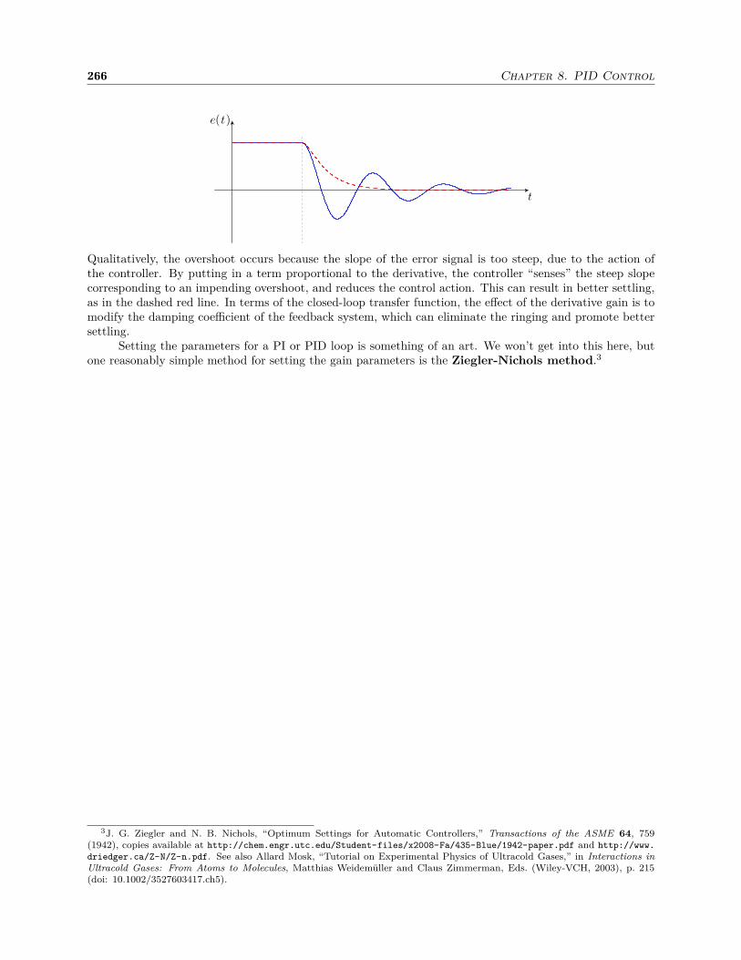
266 Chapter 8. PID Control
eo(t)
t
Qualitatively, the overshoot occurs because the slope of the error signal is too steep, due to the action ofthe controller. By putting in a term proportional to the derivative, the controller “senses” the steep slopecorresponding to an impending overshoot, and reduces the control action. This can result in better settling,as in the dashed red line. In terms of the closed-loop transfer function, the effect of the derivative gain is tomodify the damping coefficient of the feedback system, which can eliminate the ringing and promote bettersettling.
Setting the parameters for a PI or PID loop is something of an art. We won’t get into this here, butone reasonably simple method for setting the gain parameters is the Ziegler-Nichols method.3
3J. G. Ziegler and N. B. Nichols, “Optimum Settings for Automatic Controllers,” Transactions of the ASME 64, 759(1942), copies available at http://chem.engr.utc.edu/Student-files/x2008-Fa/435-Blue/1942-paper.pdf and http://www.
driedger.ca/Z-N/Z-n.pdf. See also Allard Mosk, “Tutorial on Experimental Physics of Ultracold Gases,” in Interactions inUltracold Gases: From Atoms to Molecules, Matthias Weidemüller and Claus Zimmerman, Eds. (Wiley-VCH, 2003), p. 215(doi: 10.1002/3527603417.ch5).

Part II
Digital Electronics

Chapter 9
Binary Logic and Logic Gates
9.1 Binary Logic
The idea behind binary logic is to represent information using only two states. You can call these statesTRUE and FALSE, or you can use the corresponding numerical values 1 and 0. We will explore in much moredetail how to represent and use information in this form, but for now, note that we call the fundamental(abstract) element that carries these states a bit. That is, a single bit can have either the values 0 or thevalue 1.
The idea behind digital logic and digital electronics is to represent the binary states by two differentelectronic states, usually different voltages or voltage ranges, but sometimes different currents. For example,the standard for transistor-transistor logic (TTL) is to use nominal voltages of 0 V for FALSE, and +5 Vfor TRUE. We will get into more detailed specifics later.
Changing information into a digital representation has advantages and disadvantages. The maindisadvantage of this approach is that it is necessary to sample analog signals (i.e., change continuous signalsinto discrete representations). The main advantage is in robustness to noise, as long as the noise amplitudeis far below the physical separation between the logic states (e.g., TTL logic is robust to noise interferenceprovided the noise is smaller than 5 V). Of course, for sophisticated logic systems (computers), often theadvantages far outweigh the disadvantages.
We will treat binary logic as an abstract concept for now, and learn how to manipulate binary infor-mation. Then we will come back later to the physical implementation of binary logic.
9.2 Binary Arithmetic
In binary arithmetic—the binary analogue of the more usual arithmetic—the first thing to deal with is howto represent numbers in binary. To keep things relatively simple, we will stick to representing integers inbinary (as opposed to rational approximations to real numbers, which are represented in either fixed-pointor floating-point notation, the latter of which is more complicated).
9.2.1 Unsigned Integers
The most basic form of a binary integer is an unsigned integer. Unsigned integers are just like decimalintegers, but instead of counting from 0–9 and then carrying a 1 to the next place, you just count from 0-1 andthen carry instead. (So the counting is 0, 1, 10, 11, 100, 101, 110, 111, . . . ) You can understand convertingbetween binary and decimal best via an example. Suppose that we have the unsigned integer 10112 (thesubscript “2” denotes binary, or base-2 arithmetic). There are four digits, which represent, from right to left,the “ones,” “twos,” “fours,” and “eights” places (just like the ones, tens, etc. in decimal counting). Thenproceeding from the ones (rightmost) place, or the least-significant bit (LSB), to the eights (leftmost)

270 Chapter 9. Binary Logic and Logic Gates
place, or the most-significant bit (MSB).
10112 = 1× 20 + 1× 21 + 0× 22 + 1× 23 = 1 + 2 + 8 = 11. (9.1)
Note that with N digits, we can represent 2 values with each bit, for a total of 2N numbers (i.e., rangingfrom 0 to 2N − 1).
9.2.1.1 Binary-Coded Decimal
Another representation of unsigned integers comes in binary-coded decimal (BCD), where the ideais to convert each digit in a decimal number to binary, using 4 bits per decimal number. For example,1110 = 10112, but in BCD, this would be written 00010001. This representation is “wasteful” in thatthere are 16 states for each digit but only 10 decimal digits, but this representation is very convenient forimplementations of digital numeric displays.
9.2.1.2 Hexadecimal
Hexadecimal arithmetic is just base-16 arithmetic. The 16 states are represented by 0–9 as usual, andthe “extras” by A–F for the values 10–15. Since 4 bits, or a nybble (8 bits is a byte) has 16 states, asingle hexadecimal digit is a convenient and compact representation for a binary nybble. Thus, for example,101110102 = BA16.
9.2.2 Negative Values and Sign Conventions
Besides unsigned integers, it is useful to represent negative integers in binary. There are multiple conventionsfor this, however.
9.2.2.1 Sign-Magnitude Convention
The simplest convention, the sign-magnitude convention, is to tack on an extra bit (as a new MSB) torepresent the sign, and the rest of the digits are just like an unsigned integer. For example, one nybbleranges from 0–15 as an unsigned integer, but as a signed value, it ranges from −7 to +7 as a signed integer(the three LSB’s range from 0–7, and the MSB gives the sign). Note that one value (1000) is “wasted” inthis convention, because it is not different from (0000). The main advantage is the simplicity of the scheme.You can see the relatively serious disadvantage, however, by considering a couple of example numbers,
00012 = 110, 10012 = −110. (9.2)
Unfortunately, adding these two numbers gives 10102 = −210, but really we’d like these to add to zero.
9.2.2.2 Two’s Complement
Preserving this additive-inverse property of negative numbers is the idea behind the 2’s-complement rep-resentation: if n is a positive integer, just define the number (−n) such that it satisfies n + (−n) = 0 inbinary addition. For example, suppose we have
n = 00012 = 110. (9.3)
Then −110 in 2’s-complement notation is
− n = 11112 = −110. (9.4)
To see this, first note thatn + (−n) = 100002, (9.5)
but the important point is that we drop the MSB, because we regard addition in 4-bit binary as being modulo16.
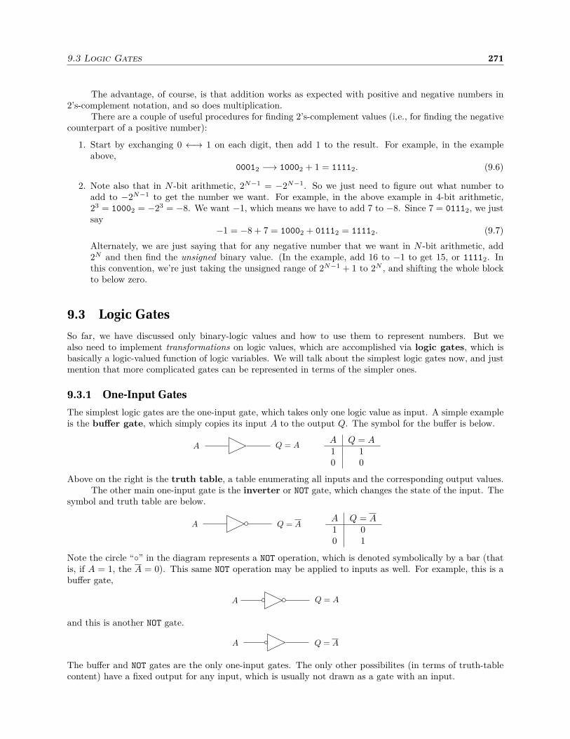
9.3 Logic Gates 271
The advantage, of course, is that addition works as expected with positive and negative numbers in2’s-complement notation, and so does multiplication.
There are a couple of useful procedures for finding 2’s-complement values (i.e., for finding the negativecounterpart of a positive number):
1. Start by exchanging 0 ←→ 1 on each digit, then add 1 to the result. For example, in the exampleabove,
00012 −→ 10002 + 1 = 11112. (9.6)
2. Note also that in N -bit arithmetic, 2N−1 = −2N−1. So we just need to figure out what number toadd to −2N−1 to get the number we want. For example, in the above example in 4-bit arithmetic,23 = 10002 = −23 = −8. We want −1, which means we have to add 7 to −8. Since 7 = 01112, we justsay
−1 = −8 + 7 = 10002 + 01112 = 11112. (9.7)
Alternately, we are just saying that for any negative number that we want in N -bit arithmetic, add2N and then find the unsigned binary value. (In the example, add 16 to −1 to get 15, or 11112. Inthis convention, we’re just taking the unsigned range of 2N−1 + 1 to 2N , and shifting the whole blockto below zero.
9.3 Logic Gates
So far, we have discussed only binary-logic values and how to use them to represent numbers. But wealso need to implement transformations on logic values, which are accomplished via logic gates, which isbasically a logic-valued function of logic variables. We will talk about the simplest logic gates now, and justmention that more complicated gates can be represented in terms of the simpler ones.
9.3.1 One-Input Gates
The simplest logic gates are the one-input gate, which takes only one logic value as input. A simple exampleis the buffer gate, which simply copies its input A to the output Q. The symbol for the buffer is below.
Q = AAA Q = A1 10 0
Above on the right is the truth table, a table enumerating all inputs and the corresponding output values.The other main one-input gate is the inverter or NOT gate, which changes the state of the input. The
symbol and truth table are below.
Q = AAA Q = A1 00 1
Note the circle “” in the diagram represents a NOT operation, which is denoted symbolically by a bar (thatis, if A = 1, the A = 0). This same NOT operation may be applied to inputs as well. For example, this is abuffer gate,
Q = AA
and this is another NOT gate.
Q = AA
The buffer and NOT gates are the only one-input gates. The only other possibilites (in terms of truth-tablecontent) have a fixed output for any input, which is usually not drawn as a gate with an input.

272 Chapter 9. Binary Logic and Logic Gates
9.3.2 Two-Input Gates
9.3.2.1 AND and NAND
Two-input gates are important, and easily available as electronic components. The first gate is the AND gate,whose symbol and truth table are shown below.
Q = A ·B = AB = A ∧BAB
A B Q = AB1 1 11 0 00 1 00 0 0
There are several notations for the AND operation in the diagram. Note that the output is only TRUE if both
inputs are TRUE.Adding a NOT to the output of the AND gate gives a NAND gate (i.e., NOT AND), which is just the negation
of the AND gate.
Q = A ·B = AB = A ∧BAB
A B Q = AB1 1 01 0 10 1 10 0 1
This gate is more important than it may seem at first glance, as we’ll return to below.
9.3.2.2 OR and NOR
The next gate is the OR gate, whose operation is symbolically represented by “+.”
Q = A + B = A ∨BAB
A B Q = A + B1 1 11 0 10 1 10 0 0
The output here is TRUE if either input is TRUE (or both inputs are TRUE). Of course, we can add a NOT tothe output.
Q = A + B = A ∨BAB
A B Q = A + B1 1 01 0 00 1 00 0 1
Thus, we obtain the NOR gate (NOT OR).
9.3.2.3 Universal Gates
The NAND and NOR gates are special, because they are universal gates. That is, any logic operation can berealized by connecting a bunch of NAND gates, or by connecting a bunch of NOR gates.
9.3.2.4 XOR and XNOR
We’ll briefly also mention the XOR gate (“exclusive OR”),
Q = A⊕BAB
A B Q = A⊕B1 1 01 0 10 1 10 0 0
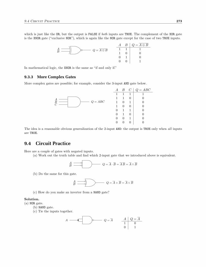
9.4 Circuit Practice 273
which is just like the OR, but the output is FALSE if both inputs are TRUE. The complement of the XOR gateis the XNOR gate (“exclusive NOR”), which is again like the NOR gate except for the case of two TRUE inputs.
Q = A⊕BAB
A B Q = A⊕B1 1 11 0 00 1 00 0 1
In mathematical logic, the XNOR is the same as “if and only if.”
9.3.3 More Complex Gates
More complex gates are possible; for example, consider the 3-input AND gate below.
Q = ABCABC
A B C Q = ABC1 1 1 11 1 0 01 0 1 01 0 0 00 1 1 00 1 0 00 0 1 00 0 0 0
The idea is a reasonable obvious generalization of the 2-input AND: the output is TRUE only when all inputsare TRUE.
9.4 Circuit Practice
Here are a couple of gates with negated inputs.(a) Work out the truth table and find which 2-input gate that we introduced above is equivalent.
Q = A ·B = A B = A ∧BAB
(b) Do the same for this gate.
Q = A + B = A ∨BAB
(c) How do you make an inverter from a NAND gate?
Solution.(a) NOR gate.
(b) NAND gate.(c) Tie the inputs together.
Q = AA A Q = A1 00 1

274 Chapter 9. Binary Logic and Logic Gates
9.5 Exercises
Problem 9.1
Convert:
(a) 8910 to 8-bit, unsigned binary
(b) −8910 to 8-bit, signed (sign-magnitude) binary
(c) −8910 to 8-bit, signed (2’s complement) binary
(d) 8910 to hexadecimal
(e) ABCD16 to decimal
(f) 01100110011001102 to hex
(g) 01100110011001102 to decimal
(h) 100110012 (2’s complement binary) to decimal
(i) 100110012 (sign-magnitude binary) to decimal
(j) 111111112 (unsigned) to decimal
Problem 9.2
Convert:
(a) 7510 to 8-bit, unsigned binary
(b) −7510 to 8-bit, signed (sign-magnitude) binary
(c) −7510 to 8-bit, signed (2’s complement) binary
(d) 7510 to hexadecimal
(e) ABBA16 to decimal
(f) 10101010101010102 to hex
(g) 10101010101010102 to decimal
(h) 110111012 (2’s complement binary) to decimal
(i) 110111012 (sign-magnitude binary) to decimal
(j) 111111012 (unsigned) to decimal
Problem 9.3
(a) Suppose x is a power of 2 (i.e., x = 2n for some positive integer n, n ∈ Z+). What does x “look”
like when written out in (unsigned) binary? (That is, how can you recognize powers of two, whenwritten in binary, just by looking at them?)
(b) In writing computer programs it is sometimes useful to check whether an integer is a power of2. (One example is in computing numerical Fourier transforms, where the most common algorithmsoperate only on arrays whose lengths are powers of 2.)
A nice trick for checking if x is a power of 2 is to compute x∧ (x−1). That is, subtract 1, and computethe bitwise AND with the original. How do you tell from the result if x is a power of 2? (You might trythis on some examples to see the pattern.)
Note: “bitwise AND” means to compute the AND of corresponding binary digits. For example, 11002 ∧10102 ≡ 11002 · 10102 = 10002.

9.5 Exercises 275
Problem 9.4
Short-question potpourri:(a) For any integer expressed in decimal, suppose you add the digits. The result is divisible by 3 if andonly if the original number is also divisible by 3. Does this statement also hold for binary numbers? Ifso, explain why. If not, provide a counterexample.
(b) What is 1000 0000 in decimal? Interpret the given number as an 8-bit, signed (2’s complement)binary number.
(c) What is 11110 in unsigned binary?
(d) What is 11110 in hex?
(e) Suppose 10102 ⊕B = 11002, where the operation is bitwise. What is B in decimal?
Problem 9.5
Short-question potpourri:(a) What is 238 457 − 3 in (unsigned) binary? (I suggest describing how to write down the binaryexpression, not actually writing it out.)
(b) What is 1010 10102 − 0101 01012? (Do the calculation in binary.)
(c) What is 11012 in hex?
(d) What is 11012 + 316? Interpret both numbers as 4-bit, 2’s complement binary numbers, and giveyour answer in 4-bit, 2’s complement binary.
(e) Suppose you generalize decimal-fraction notation (e.g., 0.9 = 9/10) to binary fractions in the obviousway (e.g., 0.12 = 1/2). What is the value of 0.12 ≡ 0.111 . . .2 (i.e., the overbar here means a repeatingdigit) in decimal?
Problem 9.6
In each expression below, assume the operation to be a bitwise logic operator. That is, it workson corresponding bits in the binary representations of the numbers; for example, a bitwise OR on twobinary numbers would look like: 000010102 + 000001102 = 000011102.
Compute the result in each case, assuming 8-bit binary arithmetic.
(a) 2510 + 7210 = ? (Give a decimal result.)
(b) 3210 · 22310 = ? (Give a decimal result.)
(c) 2310 ⊕−2310 = ? (Give a decimal result; assume signed binary, 2’s complement.)
(d) 5710 ⊕−12310 = ? (Give a decimal result; assume signed binary, 2’s complement.)
Problem 9.7
The binary bit-shift operators << and >> are defined as follows:
• n<<k (“n left-shifted by k places”) is the binary representation of n, with all bits shifted to theleft by k places (with 0’s filling in any vacated spots). Thus 00112 <<2 = 11002.
• n>>k (“n right-shifted by k places”) is the binary representation of n, with all bits shifted to theright by k places (removing any digits that “fall off the end”). Thus 01102 >>2 = 00012.
For parts (a)–(c), compute the result in each case, assuming binary arithmetic with arbitrarily manydigits allowed (i.e., no fixed number of bits like we will have in the last two parts). Don’t write out allthe digits of the answer, but give a decimal expression that doesn’t involve a bit shift operator.
(a) 2207 <<5 = ?

276 Chapter 9. Binary Logic and Logic Gates
(b) (24051 − 1)>>5 = ?
(c) (2303 + 1)<<2 = ?
For parts (d)–(e), assume fixed, 64-bit (unsigned) binary arithmetic (i.e., a fixed 64 binary “digits,”where adding 2 to the 64-bit binary representation of 263 is 02).
(d) What is the smallest integer m for which 288<<m = 0?
(e) What is the smallest integer n for which 288>>n = 0?
Chapter 10
Boolean Algebra
10.1 Algebras and Boolean Algebra
Intuitively, a Boolean algebra is an abstract, compact notation for logic (in which we will see that 1+1 = 1).A Boolean algebra is defined on the set 0, 1 (these are the “values” for Boolean variables), and has twobinary operations “+” and “·” defined, though not the usual addition and multiplication. The + operationis defined by the truth table for the OR gate, while the · operation is defined by the truth table for the AND
gate. Recall that the truth tables for the AND and OR operations on Boolean variables A and B are invariantunder the exchange of A and B, so both + and · are commutative (i.e., the order of the variables don’tmatter):
A + B = B + A, AB = BA. (10.1)
(We’re not bothering to write the “·” explicitly here.) These operations are also associative, which meansthat the order of two successive operations does not matter:
A + (B + C) = (A + B) + C, A(BC) = (AB)C. (10.2)
The other usual algebraic property that holds here is the distributive property:
A(B + C) = (AB) + (AC). (10.3)
Finally, a number of simple identities hold for the Boolean binary operators:
1. A = A
2. A · 0 = 0
3. A · 1 = A
4. A ·A = A
5. A ·A = 0
6. A + 0 = A
7. A + 1 = 1
8. A + A = A
9. A + A = 1
Roughly speaking, the NOT operation (bar) is something like a minus sign, in which case some of theseidentities seem familiar, but some seem less so (like A + 1 = 1).

278 Chapter 10. Boolean Algebra
10.2 Boolean-Algebraic Theorems and Manipulations
10.2.1 De Morgan’s Theorems
Recall the circuit practice from Section 9.4, where we examined AND and OR gates, where both inputs arenegated. For example, the negated-input AND gate is equivalent to NOR gate, as shown schematically below.
Q = A BAB = Q = A + BA
B
In algebraic notation, this is
A ·B = A + B.(10.4)
(De Morgan theorem)
Similarly
A + B = A ·B.(10.5)
(De Morgan theorem)
These are extremely useful in transforming negated expressions, as we will see.
10.2.2 Absorption Theorems
Two other useful theorems are called absorption theorems:
A + (A ·B) = A
A · (A + B) = A.
(10.6)(absorption theorems)
We will leave the proofs as exercises (in circuit practice).
10.2.3 Another Theorem
Here is another theorem that is often useful:
A + AB = A + B.(10.7)
(negated AND theorem)
We will again leave the proof as an exercise, but essentially this is saying that because of the OR with A, theA never really matters.
10.2.4 Example: XOR Gate
As an example of Boolean algebra and implementation of algebraic expressions in gates, consider the XOR
operation, where we would like to show that
A⊕B = AB + AB.(10.8)
(XOR expression)
We can first do this by working through the truth table for the right-hand side, and verifying that it matchesthe truth-table results for A⊕B.
A B AB AB A⊕B1 1 0 0 01 0 0 1 10 1 1 0 10 0 0 0 0
Now using this expression, we can show how to implement an XOR gate, in terms of regular gates.
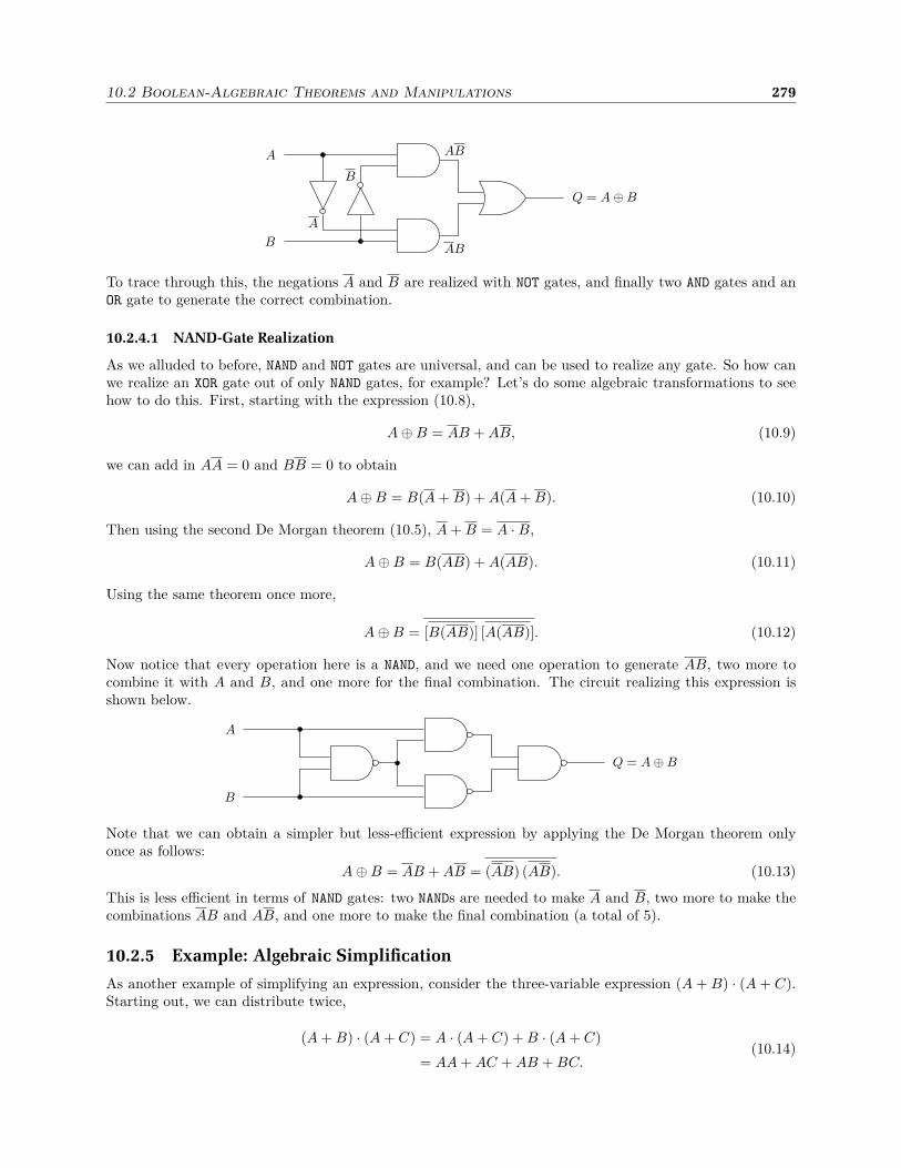
10.2 Boolean-Algebraic Theorems and Manipulations 279
Q = A⊕B
A
B
A
B
AB
AB
To trace through this, the negations A and B are realized with NOT gates, and finally two AND gates and anOR gate to generate the correct combination.
10.2.4.1 NAND-Gate Realization
As we alluded to before, NAND and NOT gates are universal, and can be used to realize any gate. So how canwe realize an XOR gate out of only NAND gates, for example? Let’s do some algebraic transformations to seehow to do this. First, starting with the expression (10.8),
A⊕B = AB + AB, (10.9)
we can add in AA = 0 and BB = 0 to obtain
A⊕B = B(A + B) + A(A + B). (10.10)
Then using the second De Morgan theorem (10.5), A + B = A ·B,
A⊕B = B(AB) + A(AB). (10.11)
Using the same theorem once more,
A⊕B = [B(AB)] [A(AB)]. (10.12)
Now notice that every operation here is a NAND, and we need one operation to generate AB, two more tocombine it with A and B, and one more for the final combination. The circuit realizing this expression isshown below.
Q = A⊕B
A
B
Note that we can obtain a simpler but less-efficient expression by applying the De Morgan theorem onlyonce as follows:
A⊕B = AB + AB = (AB) (AB). (10.13)
This is less efficient in terms of NAND gates: two NANDs are needed to make A and B, two more to make thecombinations AB and AB, and one more to make the final combination (a total of 5).
10.2.5 Example: Algebraic Simplification
As another example of simplifying an expression, consider the three-variable expression (A + B) · (A + C).Starting out, we can distribute twice,
(A + B) · (A + C) = A · (A + C) + B · (A + C)
= AA + AC + AB + BC.(10.14)

280 Chapter 10. Boolean Algebra
Then AA = A, and using the first absorption theorem in Eqs. (10.6) to write A + AC = A,
(A + B) · (A + C) = (A + AC) + AB + BC
= A + AB + BC.(10.15)
Then also A + AB = A, so(A + B) · (A + C) = A + BC, (10.16)
a somewhat simpler expression (two operations vs. three).
10.3 Karnaugh Maps
It can often be difficult to see how to realize a particular logic function in terms of logic gates, just viaalgebraic manipulations. One tool that makes this more intuitive, at least for small numbers of inputs (3 or4), is the Karnaugh map. (The cases of 1 and 2 inputs we’ve already mostly covered with standard gates,and it’s easy to do these exhaustively.) These days, computers can exhaustively search logical expressionsto find the simplest ones, so you might ask, why bother with techniques like the Karnaugh map for doingalgebra? Well, algebraic simplicity is a subjective thing (depending somewhat on the goals of the particularproblem at hand), and symbolic manipulation systems on computers have notoriously poor “taste” when itcomes to “simple.” The Karnaugh map is also such an elegant and downright cool tool that it’s really worthstudying.
The first idea behind a Karnaugh map is to make a 2D table of logic inputs and truth-table values.The second twist is to order the inputs using a 2-bit Gray code, which means that we count as 00, 01, 11,10, instead of the usual binary-counting order. The point is when counting this way we change only 1 bitat a time (in regular binary, this doesn’t happen when we count from 01 to 10). The motivation for Graycodes comes from mechanical implementations of logic, where you may get spurious transitional states if bitsdon’t change synchronously (this happens in some fast logic circuits as well). That is, when counting from01 to 10, the actual sequence may be 01 to 00 to 10 if the LSB changes before the MSB. In terms of theKarnaugh map, the idea is to keep “related” input states grouped together.
The process of hunting for simplifications in a Karnaugh map is hard to explain, but it’s easy to getthe idea by studying a few examples.
10.3.1 Three-Input Example
Before, as a Boolean-algebraic example, we showed in Eq. (10.16) that
(A + B) · (A + C) = A + BC. (10.17)
We will show how to obtain this and other transformations via the Karnaugh map. The first task is to writeout the diagram as a table. Notice that the four values of AB are along the top, in Gray-coded order, andthe two C values are along the side. We are also writing out each output value for each set of possible inputvalues, so this is just a truth table in 2D form, here for (A + B) · (A + C).
AB
C00 01 11 10
0
1 1
1
1
1
1
0
0
0
Now to analyze this, the idea is to look for blocks of 1’s in square or rectangular shapes (2× 1, 2× 2, etc.).One example is below.
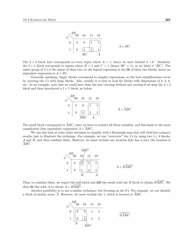
10.3 Karnaugh Maps 281
AB
C00 01 11 10
0
1 1
1
1
1
1
0
0
0
ABC
A + BC
The 2 × 2 block here corresponds to every input where A = 1, hence we have labeled it “A.” Similarly,the 2 × 1 block correponds to inputs where B = 1 and C = 1 (hence BC = 1), so we label it “BC.” Theentire group of 1’s is the union of these two, so the logical expression is the OR of these two blocks, hence anequivalent expression is A + BC.
Generally speaking, bigger blocks correspond to simpler expressions, so the best simplifications occurby covering the 1’s with large blocks. Also, usually it is best to look for blocks with dimensions of 2, 4, 8,etc. As an example, note that we could have done the last covering without any overlap if we kept the 4× 4block and then introduced a 1× 1 block, as below.
AB
C00 01 11 10
0
1 1
1
1
1
1
0
0
0
AABC
A + ABC
The small block corresponds to ABC, since we have to restrict all three variables, and this leads to the morecomplicated (but equivalent) expression A + ABC.
We can also look at some other attempts to simplify with a Karnaugh map that will yield less compactresults, just to illustrate the technique. For example, we can “overcover” the 1’s by using two 4× 4 blocks,A and B, and then combine them. However, we must exclude one location that has a zero; the location isABC.
AB
C00 01 11 10
0
1 1
1
1
1
1
0
0
0
AB
ABC
A + BABC
Thus, to combine these, we negate the null block and AND the result with the B block to obtain BABC. We
then OR this with A to obtain A + BABC.Another possibility is to use a similar technique, but focusing on the 0’s. For example, we can identify
a block of mostly zeros, A. However, we must exclude the 1, which is located at ABC.
AB
C00 01 11 10
0
1 1
1
1
1
1
0
0
0
AABC
A ABC
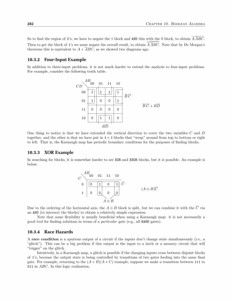
282 Chapter 10. Boolean Algebra
So to find the region of 0’s, we have to negate the 1 block and AND this with the 0 block, to obtain A ABC.
Then to get the block of 1’s we must negate the overall result, to obtain A ABC. Note that by De Morgan’stheorems this is equivalent to A + ABC, as we showed two diagrams ago.
10.3.2 Four-Input Example
In addition to three-input problems, it is not much harder to extend the analysis to four-input problems.For example, consider the following truth table.
AB
CD00 01 11 10
00
01
11
10
1
1
1 1 1
1
1 10
0
0
0
0
0
0
0
B C
BD
B C + BD
One thing to notice is that we have extended the vertical direction to cover the two variables C and Dtogether, and the other is that we have put in 4× 4 blocks that “wrap” around from top to bottom or rightto left. That is, the Karnaugh map has periodic boundary conditions for the purposes of finding blocks.
10.3.3 XOR Example
In searching for blocks, it is somewhat harder to see XOR and XNOR blocks, but it is possible. An example isbelow.
AB
C00 01 11 10
0
1
1 10
0 0 0
0
0
C
A⊕B
(A⊕B)C
Due to the ordering of the horizontal axis, the A ⊕ B block is split, but we can combine it with the C viaan AND (to intersect the blocks) to obtain a relatively simple expression.
Note that some flexibility is usually beneficial when using a Karnaugh map: it is not necessarily agood tool for finding solutions in terms of a particular gate (e.g., all NAND gates).
10.3.4 Race Hazards
A race condition is a spurious output of a circuit if the inputs don’t change state simultaneously (i.e., a“glitch”). This can be a big problem if this output is the input to a latch or a memory circuit that will“trigger” on the glitch.
Intuitively, in a Karnaugh map, a glitch is possible if the changing inputs cross between disjoint blocksof 1’s, because the output state is being controlled by transitions of two gates feeding into the same finalgate. For example, returning to the (A + B)(A + C) example, suppose we make a transition between 111 to011 in ABC. In this logic realization,
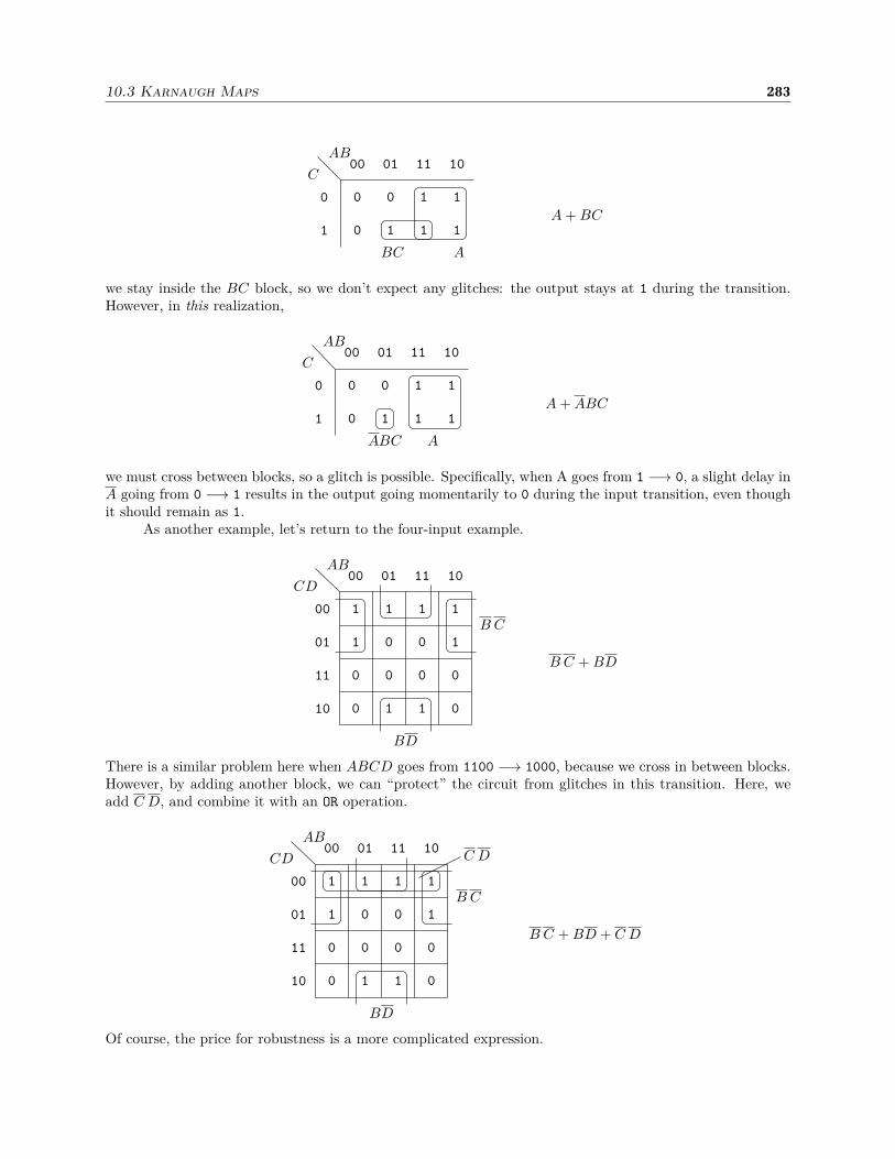
10.3 Karnaugh Maps 283
AB
C00 01 11 10
0
1 1
1
1
1
1
0
0
0
ABC
A + BC
we stay inside the BC block, so we don’t expect any glitches: the output stays at 1 during the transition.However, in this realization,
AB
C00 01 11 10
0
1 1
1
1
1
1
0
0
0
AABC
A + ABC
we must cross between blocks, so a glitch is possible. Specifically, when A goes from 1 −→ 0, a slight delay inA going from 0 −→ 1 results in the output going momentarily to 0 during the input transition, even thoughit should remain as 1.
As another example, let’s return to the four-input example.
AB
CD00 01 11 10
00
01
11
10
1
1
1 1 1
1
1 10
0
0
0
0
0
0
0
B C
BD
B C + BD
There is a similar problem here when ABCD goes from 1100 −→ 1000, because we cross in between blocks.However, by adding another block, we can “protect” the circuit from glitches in this transition. Here, weadd C D, and combine it with an OR operation.
AB
CD00 01 11 10
00
01
11
10
1
1
1 1 1
1
1 10
0
0
0
0
0
0
0
B C
BD
C D
B C + BD + C D
Of course, the price for robustness is a more complicated expression.

284 Chapter 10. Boolean Algebra
10.4 Circuit Practice
10.4.1 Boolean-Algebra Theorems
Here, you should prove two things that we only introduced earlier.
(a) Prove the first absorption theorem in Eqs. (10.6):
A + (A ·B) = A. (10.18)
Use a truth table or algebra.(b) Prove the second absorption theorem in Eqs. (10.6):
A · (A + B) = A. (10.19)
Solution.(a) First suppose B = 0. Then
A ·B = A · 0 = 0, (10.20)
and soA + (A ·B) = A + 0 = A. (10.21)
Now take the other case, where B = 1. Then
A ·B = A · 1 = A, (10.22)
and soA + (A ·B) = A + A = A. (10.23)
(b) Using the same method, first suppose B = 0. Then
A + B = A + 0 = A, (10.24)
and soA · (A + B) = A ·A = A. (10.25)
Now taking the other case B = 1,A + B = A + 1 = 1, (10.26)
and soA · (A + B) = A · 1 = A. (10.27)
10.4.2 Karnaugh Map
Write down the Karnaugh map and a logic circuit for the following function: the output is 1 if and only ifthe input, a 3-bit unsigned integer, is prime. (Don’t count 0, 1, or 2 as prime integers.)
Solution. The primes are 3, 5, and 7. In binary, these are 011, 101, and 111. Hence the Karnaughmap:
AB
C00 01 11 10
0
1 1 1 1
0
0
0 00
(A + B)C(A + B)C
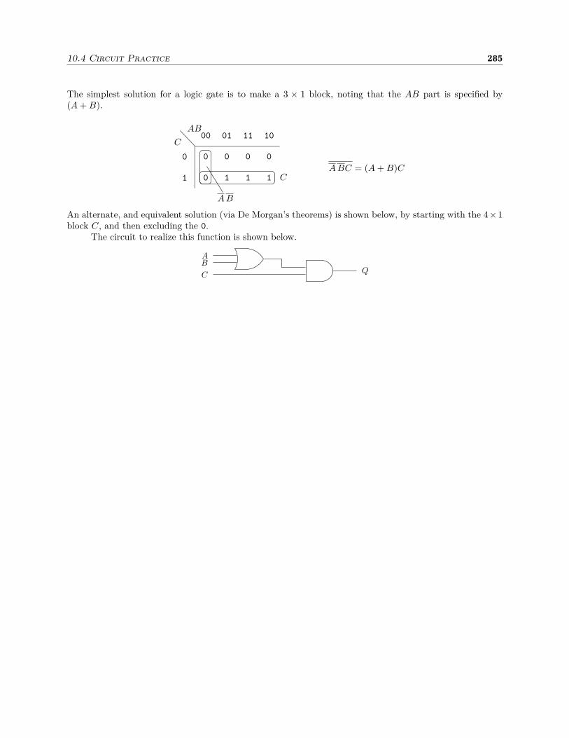
10.4 Circuit Practice 285
The simplest solution for a logic gate is to make a 3 × 1 block, noting that the AB part is specified by(A + B).
AB
C00 01 11 10
0
1 1 1 1
0
0
0 00
C
A B
A BC = (A + B)C
An alternate, and equivalent solution (via De Morgan’s theorems) is shown below, by starting with the 4×1block C, and then excluding the 0.
The circuit to realize this function is shown below.
AB
CQ

286 Chapter 10. Boolean Algebra
10.5 Exercises
Problem 10.1
Simplify the expressionQ = A B C + A BC + ABC + AB C, (10.28)
and draw a logic circuit that realizes it. (This can be done with only 3 2-input gates and 1 3-inputgate; try to at least reduce this somewhat, and it’s best if your solution reflects the symmetry of theoriginal expression. Also, try to use algebraic transformations rather than writing out truth tables.)
Problem 10.2
Simplify the expressionQ = ABC + A BC + ABC + AB C, (10.29)
and draw a logic circuit that realizes it. (This is possible with only 1 3-input gate; try to at leastreduce this somewhat, and it’s best if your solution reflects the symmetry of the original expression.Also, try to use algebraic transformations rather than writing out truth tables.)
Problem 10.3
(a) Simplify the following Boolean expression:
Q = (A + B)(B + A) + AB + A + B + B. (10.30)
(b) Sketch a realization of this expression (after simplifying!) using only 2-input NAND gates.
Problem 10.4
(a) Simplify the following Boolean expression:
Q = (A + B)(A + B) + (A + B)(A + B). (10.31)
(b) Sketch a realization of this expression (after simplifying!) in terms of only XNOR gates.
Problem 10.5
(a) Simplify the following Boolean expression:
Q =[
(A BC)(B AC)][
(AB)(ABC)]
. (10.32)
(b) Sketch a realization of this expression (after simplifying!) in terms of only NOR gates.
Problem 10.6
Simplify the following Boolean expression:
Q = A + B + C + D + E
+ AB + BC + CD + DE + EA
+ ABC + BCD + CDE + DEA + EAB
+ ABCD + BCDE + CDEA + EABC
+ ABCDE.
(10.33)

10.5 Exercises 287
Problem 10.7
Consider the following circuit, based on 3-input NAND gates.
A
C
B Q
(a) Write down the logic (Boolean) expression for the circuit.
(b) Write down the truth table.
Problem 10.8
Consider the following circuit, based on 3-input NOR gates.
A
C
B Q
(a) Write down the logic (Boolean) expression for the circuit.
(b) Write down the truth table.
Problem 10.9
Show how you can realize an XOR gate (A⊕B = A ·B + A ·B) using only NOR gates.
Problem 10.10
Show how you can realize an XNOR gate (A⊕B = A ·B + A ·B) using only NAND gates.
Problem 10.11
One possible generalization of boolean logic is to three states: the usual TRUE (1) and FALSE (0), plusa third UNKNOWN (?) state. The (still associative and distributive) operations + and · can then bedefined by the following:
• if A and B are both Boolean (i.e., either 0 or 1), the result is just the Boolean result.
• A + 1 = 1 for any A (including ?)
• A · 0 = 0 for any A (including ?)
• ? + 0 = ?

288 Chapter 10. Boolean Algebra
• ? + ? = ?
• ? · 1 = ?
• ? · ? = ?
• A is the same as in Boolean algebra if A is 0 or 1, and ? otherwise.
(Think through how these rules sensibly generalize Boolean algebra, where UNKNOWN means “could beeither TRUE or FALSE.”)
Prove that both De Morgan theorems still hold in this generalized logic algebra. You can do this bytruth table, but try to be more clever, breaking the proof down into cases you can work out algebraically.
Problem 10.12
(a) Show that the XOR operation is both commutative and associative. (You may assume + and · arecommutative and associative.)
(b) Simplify the following Boolean expression. (Eliminate any constant values, 0 or 1, from your finalexpression.)
Q =
[
[
[
[(A⊕B)⊕ (A⊕B)⊕ (A⊕ C)]⊕B]
⊕ C]
⊕ C
]
. (10.34)
Problem 10.13
Write out the Karnaugh map for a circuit where the output is true if the input (a 3-bit, unsignedinteger, 0–7) is in the Fibonacci sequence. Give a circuit implementation in terms of 2-input gates.
Problem 10.14
Write out the Karnaugh map for a circuit where the output is true if the input (a 3-bit, unsignedinteger, 0–7) is one of the first 6 digits of π. Give a circuit implementation in terms of 2-input gates.
Problem 10.15
A semiprime number is a positive integer that is the product of two prime numbers. The primenumbers need not be distinct, 1 doesn’t count as one of the primes. For example, 0–3 are not semiprime,but 4 is.
(a) Write down the Karnaugh map for the function of the boolean variables A, B, C, and D, which istrue when the concatenation ABCD (when converted to decimal as an unsigned integer) is semiprime.
(b) Find a (reasonably simple) boolean expression for this 4-bit semiprime function you diagrammedin (a).
(c) Sketch a logic implementation of this function in terms of logic gates.
Problem 10.16
(a) Write down the Karnaugh map for the function of the Boolean variables A, B, C, and D, whichis true when the concatenation ABCD (when converted to decimal as an unsigned integer) is greaterthan or equal to 6.
(b) Find a (reasonably simple) boolean expression for the logic function you diagrammed in (a).
(c) Sketch a logic implementation of this function in terms of only 2-input NAND gates.

10.5 Exercises 289
Problem 10.17
Find logic to perform multiplication of two 2-bit (unsigned) integers (i.e., 0–3), with a 4-bit output.Hint: use a separate Karnaugh map for each output bit.1
Problem 10.18
Find logic to perform addition of two 2-bit (unsigned) integers (i.e., 0–3), with a 3-bit output.Hint: use a separate Karnaugh map for each output bit.
Problem 10.19
(a) Write down the Karnaugh map for the function of the Boolean variables A, B, C, and D, which istrue when ABCD (when converted to decimal as an unsigned integer, D being the LSB) is odd and
greater than 4.
(b) Find a (reasonably simple) boolean expression for the logic function you diagrammed in (a).
(c) Sketch a logic implementation of this function in terms of only 2-input NAND gates.
Problem 10.20
(a) Write down the Karnaugh map for the function of the Boolean variables A, B, C, and D, whichis true when ABCD (when interpreted as an unsigned integer, D being the LSB) is valid as a BCDinteger.
(b) Find a (reasonably simple) boolean expression for the logic function you diagrammed in (a).
(c) Sketch a logic implementation of this function in terms of only 2-input NOR gates.
Problem 10.21
Consider the Boolean expression
Q = (A + B) + AC + C(A + B). (10.35)
(a) Write down the Karnaugh map for this expression, and find a simpler (equivalent) expression.Indicate the blocks corresponding to the three terms in the logical expression above.
(b) This expression has a race hazard; find it and explain the problem (i.e., give the initial and finalstates of ABC, and explain what needs to happen to produce a spurious output state).
1Paul Horowitz and Winfield Hill, The Art of Electronics, 2nd ed. (Cambridge, 1989), Exercise 8.14 (ISBN: 0521370957).


Chapter 11
Physical Implementation of Logic Gates
So far, we have studied logic and logic gates, but logic is much more useful if we can implement logic gatesphysically. Generally speaking you can buy these as prepackaged integrated circuits, but it is still usefulto understand how to implement these, for (1) extra intuition and (2) to understand the limits and quirksof commonly available electronic logic gates. We will start with simple examples of logic realizations andprogress to realistic (but more complicated) cases.
The material here in this chapter relies on previous material on diodes from Chapter 3 and transistorsfrom Chapter 4. However, we will briefly review some of the relevant material here.
11.1 Simple Mechanical Switches
Fundamentally, electronic logic gates work by involving switches. Typically these are some form of electronic
switches, but of course these can be ordinary mechanical switches (equivalent to connecting two points bya wire or breaking the wire connection). One simple convention for a single-pole, single-throw (SPST)switch (“single pole” = single circuit to break or connect; “single throw” = single possible connection tomake or break), as shown below, is that the closed (conducting) or ON state is TRUE,
closed = TRUE
and the open or OFF state is FALSE.
open = FALSE
This convention agrees with a common convention for logic in terms of voltage levels, where HIGH voltage isTRUE and LOW voltage is FALSE, if we consider a relay (magnetically controlled switch), as shown below.
Vin
Vin = V+ −→ TRUE
Vin = 0 −→ FALSE
The relay is pulled closed when the voltage is HIGH (at some voltage V+), due to the magnetic field of thecoil; when the voltage is zero, there is no field and the switch pops open (due to the action of a spring).
Using switches it is easy to see how to construct an AND gate, if two switches are in series, since bothswitches must close to light the light bulb (the logical “output” here).

292 Chapter 11. Physical Implementation of Logic Gates
For an OR gate, the two switches are in parallel, so only one switch needs to be closed to light the bulb.
As a final example, an inverter is shown below.
T
F +V
The switch here is a single-pole, double-throw (SPDT) switch (“double throw” = two alternativecontacts for the switch), where “up” on the switch is TRUE and “down” on the switch is FALSE.
11.2 Diode Logic (DL)
The simples “purely electronic” examples of logic come in the form of diode logic (DL). Before examiningsome DL gates, first let’s review how diodes work.
11.2.1 Diode Review
A diode is a two-terminal device, as shown below, and it acts as a one-way valve for current: current canonly flow from the anode to the cathode (in the direction of the “diode arrow” in the schematic symbol).
I−→anode cathode
That is, as in the diagram below, if the anode voltage VA is greater than the cathode voltage VB , thencurrent flows; otherwise, no current flows.
I−→A B =
I−→or
(I = 0)A B A B
if VA > VB if VA < VB
You can think of the diode as being a short circuit in the first case (“forward-biased”), and an open circuitin the second (“reverse-biased”). However, the real situation is a bit more complicated: a slightly bettermodel is that there is a forward voltage drop of around 0.6 to 0.7 V when the diode is conducting current(at least for a small-signal silicon diode).

11.2 Diode Logic (DL) 293
11.2.2 DL AND Gate
Now to see how to realize gates in DL. Below is a realization of an AND gate. The DL convention here is that0 V is FALSE, and +5 V is TRUE.
A
B Q = AB
R
+5 V
If both inputs are at +5 V then all points are at the same voltage, including the output Q. If one input islow, say A, then the situation is as shown below.
A
Q = 0 V (actually ∼0.6 V)
R
+5 V
The diode is forward-biased, and thus shorts the output Q to ground. The power-supply voltage (+5 V) isdropped across the resistor because the diode causes sufficient current to flow through the resistor to groundto ensure this. The state of the other input (B) is irrelevant here, because either it “agrees” with A, or if itis HIGH, B’s diode is reverse-biased, so it is disconnected from the circuit.
Actually, the output voltage is not quite 0 V in the latter case; because the diode has a forward-voltagedrop, the output FALSE state is more like 0.6 V.
11.2.3 DL OR Gate
Another DL gate, the OR gate, is shown below.
A
B R
Q = A + B
Here, if either input is at +5 V, then the corresponding diode is forward-biased, so output is at +5 V [actually,(+5 − 0.6) V if we account for the diode’s voltage drop]. If both inputs are at 0 V, then the whole circuit,including the output, is also at 0 V.
The main problem in the DL circuits is that one of the signal-voltage states “degrades” by 0.6 V oneach gate, so not many gates can be cascaded while keeping the signal levels distinguishable. This motivatesthe use of active devices in logic circuits that can maintain the proper voltage levels.
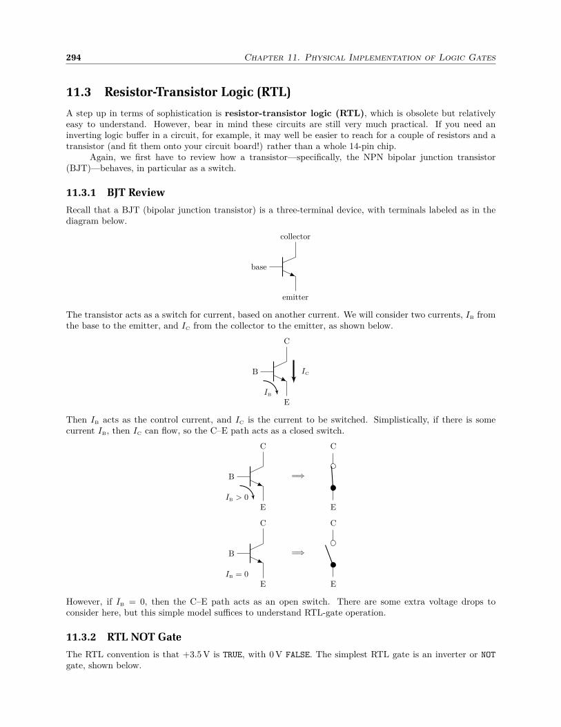
294 Chapter 11. Physical Implementation of Logic Gates
11.3 Resistor-Transistor Logic (RTL)
A step up in terms of sophistication is resistor-transistor logic (RTL), which is obsolete but relativelyeasy to understand. However, bear in mind these circuits are still very much practical. If you need aninverting logic buffer in a circuit, for example, it may well be easier to reach for a couple of resistors and atransistor (and fit them onto your circuit board!) rather than a whole 14-pin chip.
Again, we first have to review how a transistor—specifically, the NPN bipolar junction transistor(BJT)—behaves, in particular as a switch.
11.3.1 BJT Review
Recall that a BJT (bipolar junction transistor) is a three-terminal device, with terminals labeled as in thediagram below.
base
collector
emitter
The transistor acts as a switch for current, based on another current. We will consider two currents, IB fromthe base to the emitter, and IC from the collector to the emitter, as shown below.
B
C
E
IC
IB
Then IB acts as the control current, and IC is the current to be switched. Simplistically, if there is somecurrent IB, then IC can flow, so the C–E path acts as a closed switch.
B
C
EIB > 0
=⇒
C
E
B
C
EIB = 0
=⇒
C
E
However, if IB = 0, then the C–E path acts as an open switch. There are some extra voltage drops toconsider here, but this simple model suffices to understand RTL-gate operation.
11.3.2 RTL NOT Gate
The RTL convention is that +3.5 V is TRUE, with 0 V FALSE. The simplest RTL gate is an inverter or NOT
gate, shown below.

11.4 The Real Thing: Transistor-Transistor Logic (TTL) 295
450 Ω
A
Q = A
640 Ω
+3.5 V
If the input is TRUE, then IB > 0, and the C–E path conducts. This pulls the output down near ground, orFALSE. If the input is FALSE, then IB = 0, and the C–E path is broken. The resistor pulls the output up tothe supply voltage, or TRUE.
11.3.3 RTL NOR Gate
A slightly more complicated example is the NOR gate, shown below.
450 Ω
A
450 Ω
BQ = A + B
640 Ω
+3.5 V
The operation is the same as the NOT gate, but here either input can pull the output to ground; the outputis only pulled up HIGH in voltage if both inputs are FALSE or LOW.
RTL works reasonable well and doesn’t suffer from the (cumulative) degradation problems of DL,because the output levels are set by the supply levels, not the inputs. However, DL is obsolete because the“return” to the high state when the transistors stop conducting is via the pull-up resistor. This transition isslow if there is a significant capacitive load on the output. (The LOW transitions when the transistors conductare fast because the BJT collectors have effectively a very low impedance.)
11.4 The Real Thing: Transistor-Transistor Logic (TTL)
A common standard still in modern use is transistor–transistor logic (TTL). The nominal conventionis that +5 V is TRUE, and 0 V is FALSE. The circuitry is somewhat more complicated, and we’ll go throughthe classic TTL NAND gate, shown below, as an example.

296 Chapter 11. Physical Implementation of Logic Gates
A
B
Q1
Q2
Q3
Q4
1.6 kΩ4 kΩ130 Ω
+5 V
1 kΩ
Q = AB
input stage phase splitter totem-pole output
There are three different stages: the input stage (Q1), the phase splitter (Q2), and the totem-pole output(Q3, Q4, and the diode). An unusual feature is the double-emitter input transistor Q1. It works just like aregular transistor, except that a base current to either emitter will switch the collector current. Let’s tracethe voltages through the circuit for two cases.
1. Suppose A or B is LOW. Then:
• Q1 is ON (collector conducts to grounded input).
• Q2’s base is LOW, thus Q2 is OFF.
• Q3’s base is HIGH (pulled up by 1.6-kΩ resistor), thus Q3 is ON.
• Q4’s base is LOW (pulled down by 1-kΩ resistor), thus Q4 is OFF.
• The output is HIGH since it is pulled up via Q3 and the diode. The output is 5 V−Q3’s voltagedrop− the diode drop, which works out to around 3.5 V.
2. Suppose A and B are both HIGH. Then:
• Q1 is OFF (collector disconnected from inputs).
• Q2’s base is HIGH (pulled up via the B–C path of Q1, which acts like a diode), thus Q2 is ON.
• Q2’s emitter is pulled LOW by Q4, which is ON.
• Q2’s collector is pulled LOW since it is ON; so Q4’s base is LOW, and Q3 is OFF.
• The output is LOW since it is pulled down via Q4. The output is 0 V + Q4’s voltage drop, whichworks out to around 0.4 V.
The point of all this is to generate a few useful and general observations.
1. The inputs “want” to be high, because they tend to be pulled up to the power-supply voltage via the4-kΩ resistor and the B–E paths of Q1. Thus, the inputs source current when they are pulled LOW. Inparticular, open inputs are HIGH by default in TTL, and less current flows (less power is dissipated)when the inputs are HIGH. In particular, if you have unused inputs in TTL circuits, it is best to tiethem HIGH (i.e., connect them to +5 V).
2. The output, when driving another TTL input, must sink current, roughly (5 V)/(4 kΩ) = 1.25 mA.One output can drive multiple inputs, but there is a limit to this, because the output has a limitedcurrent capacity. This limit is called fanout, which is typically ∼10 inputs for a standard TTL output.

11.5 The Modern Thing: CMOS Logic 297
3. The output voltages don’t quite match the nominal values of 0 V and +5 V, so the TTL standarddefines precisely the tolerance limits on signal voltages.
• TTL circuits must recognize anything from +2.0 V to +5 V as HIGH.
• TTL circuits must recognize anything from 0 V to +0.8 V as LOW.
• The intermediate range of +0.8 V to +2.0 V is indeterminate: TTL circuits can do anything withinputs in this range and still conform to the TTL standard.
11.4.1 TTL Nomenclature
Standard TTL chips are most famously grouped into the 74XX (or 74XXX) family. For example, there are:
• 7400: quad, 2-input NAND (i.e., 4 NAND’s per package)
• 7402: quad, 2-input NOR
• 7404: hex inverter (i.e., 6 NOT gates)
• 7408: quad, 2-input AND
and there are hundreds more, though many are now becoming obsolete. Note that these are also labeled asequivalent 54XX circuits, which are the military-grade versions.
These “classic” TTL circuits are now obsolete, but they still come in many popular “flavors.” Thesevariations are labeled by a tag between the 74 and XX, for example 74LS00, 74F00, and 74HCT00 are allbasically the same as the original 7400. The common flavors are:
• L: low-power (slow, obsolete)
• H: high-speed (high-speed, obsolete)
• S: high-speed Schottky (high-power, obsolete)
• LS: low-power Schottky (common, modern-standard chip)
• AS, ALS: “advanced” S, LS
• F: fast (gates have ∼4-ns propagation delay vs. ∼10 ns for standard gates)
11.5 The Modern Thing: CMOS Logic
11.5.1 MOSFET Review
We have seen MOSFETs before in Section 5.2 while studying the analog side of electronics. Before seeinghow they’re used in making digital gates, we’ll briefly review their operation, in a relatively simplistic waythat suffices to explain their digital utility.
Recall that the MOSFET is a four-terminal device, with terminals labeled as in the diagram below.
gatebody
drain
source
n-channel
gatebody
drain
sourcep-channel

298 Chapter 11. Physical Implementation of Logic Gates
To keep things simple, think of the body connection relatively ignorable compared to the others (it’s usuallyshorted to the source lead), so this is more or less a three-terminal device. In this case, the current to becontrolled (ID for “drain current”) runs from drain to source in the n-channel MOSFET, while current runsfrom source to drain in the p-channel flavor (for this reason, the p-channel version is typically drawn in aninverted sense compared to what appears above).
Like the BJT, the MOSFET acts as a switch for current. However, while the BJT was controlled byanother current (the base current), the MOSFET is controlled by a voltage—namely, the gate–source voltageVGS. First, consider the n-channel MOSFET. Speaking simplistically, if there is a sufficiently positive gatevoltage (referenced to the source), then ID can flow. If there is zero gate voltage, then no current flows. Thus,the MOSFET acts as a voltage-controlled switch (recall the MOSFET analog switch from Section 5.4.5).
G
D
SVGS = +V
=⇒
D
S
G
D
SVGS = 0
=⇒
D
S
For the moment, we won’t worry too much about how positive VGS must be to close the switch, but typicallyin the ON state, VGS is at least as large as any voltage that would be presented to the drain terminal. Anddon’t worry, we’ll come back to how the p-channel MOSFET works, after we take the n-channel version fora test drive. But one more thing to note before carrying on is that the gate is electrically isolated from therest of the transistor by an oxide insulating layer (the “O” in “MOSFET” is for “oxide”). The consequenceof this is that there is some capacitance between the gate and the other terminals, which is important inconsidering the speed of MOSFET switching.
11.5.2 NMOS
Other than being under voltage control, the n-channel MOSFET can be used in much the same way as annpn transistor to make gates in the RTL style of Section 11.3, to make NMOS logic gates (the “N” herereferring to n-channel FETs). For example, a NOT gate is shown below.
+V
+V
0+V
0
This behaves in much the same way as the RTL NOT gate of Section 11.3.2. With zero input voltage (VGS = 0),the MOSFET behaves as an open switch, so the output gets pulled up via the resistor to +V . With a positiveinput voltage, the MOSFET acts as a closed switch, so the output is actively pulled close to ground.

11.5 The Modern Thing: CMOS Logic 299
Other NMOS gates are of course possible. By putting two MOSFETs in parallel the circuit belowrealizes a NOR gate, in the same manner as the RTL NOR gate of Section 11.3.3.
A
B
+V
Q
Again, either transistor can pull the output to ground, which means that either input being HIGH leads toa LOW output. A NAND gate can be made in a similar way by putting the two transistors in series with theresistor, so that both transistors must be activated to bring the output low. We’ll see an example like thisin the next section.
The main disadvantages of NMOS are in speed and power consumption. Like RTL, the resistorhas a limited current available to pull the output up to +V in an upward transition. Also, the inputgate capacitance is a limitation to speed—especially when the resistor of one logic gate drives the inputcapacitance of the next gate. In terms of power consumption, note that (like RTL and TTL) the logic gatedraws quiescent current whenever the output is LOW (i.e., even if the gate isn’t driving any load) because ofthe nature of the pull-up resistor.
11.5.3 PMOS
In contrast to the relatively asymmetric RTL and TTL standards, where the npn BJT was king, the p-channel MOSFET is an important counterpart to the n-channel version. The p-channel FET works just likethe n-channel, but with the currents and voltages reversed. The diagram below summarizes this.
G
S
D
VGS = −V
=⇒
S
D
G
S
D
VGS = 0
=⇒
S
D
Again the current to be switched flows from source to drain. A zero gate voltage (with respect to the source,which is now drawn as the upper terminal) still causes the “switch” to be open. To close the MOSFETswitch, a negative gate voltage (again, with respect to the source, so VGS < 0) is required to close the gate.
The p-channel MOSFET can be used in just the same way as the n-channel to realize its own logicfamily, the PMOS logic family. The NOT gate is shown below, and is basically the mirror image of the
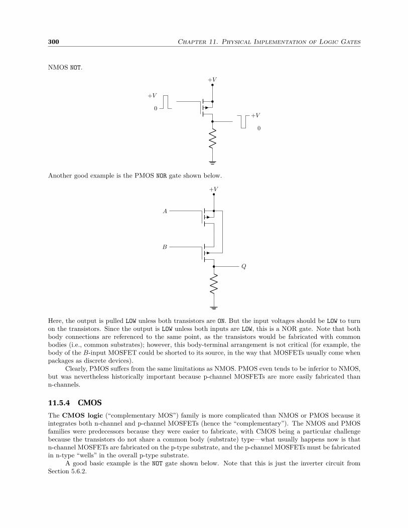
300 Chapter 11. Physical Implementation of Logic Gates
NMOS NOT.
+V
+V
0
+V
0
Another good example is the PMOS NOR gate shown below.
+V
Q
A
B
Here, the output is pulled LOW unless both transistors are ON. But the input voltages should be LOW to turnon the transistors. Since the output is LOW unless both inputs are LOW, this is a NOR gate. Note that bothbody connections are referenced to the same point, as the transistors would be fabricated with commonbodies (i.e., common substrates); however, this body-terminal arrangement is not critical (for example, thebody of the B-input MOSFET could be shorted to its source, in the way that MOSFETs usually come whenpackages as discrete devices).
Clearly, PMOS suffers from the same limitations as NMOS. PMOS even tends to be inferior to NMOS,but was nevertheless historically important because p-channel MOSFETs are more easily fabricated thann-channels.
11.5.4 CMOS
The CMOS logic (“complementary MOS”) family is more complicated than NMOS or PMOS because itintegrates both n-channel and p-channel MOSFETs (hence the “complementary”). The NMOS and PMOSfamilies were predecessors because they were easier to fabricate, with CMOS being a particular challengebecause the transistors do not share a common body (substrate) type—what usually happens now is thatn-channel MOSFETs are fabricated on the p-type substrate, and the p-channel MOSFETs must be fabricatedin n-type “wells” in the overall p-type substrate.
A good basic example is the NOT gate shown below. Note that this is just the inverter circuit fromSection 5.6.2.

11.5 The Modern Thing: CMOS Logic 301
Q1
Q2
+V
+V
0
+V
0
With a zero input, Q1 is OFF and Q2 is ON, so the output is pulled (actively) up to +V . With a positiveinput, the transistors exchange states, so the output is pulled (actively) down to ground.
Note that the complementary arrangement eliminates the resistor of NMOS/PMOS, along with itsdisadvantages.
Some important observations we can make from this circuit that hold true more generally for CMOSgates are:
1. Because there is only one path of significant conductance from the output, there is no quiescent current.
2. The output is actively pulled to the appropriate state via a low-impedance path, so that the transitionsare relatively fast (and relatively symmetric in terms of speed).
3. Indeed, an important characteristic of CMOS is low power consumption while the gates are static,punctuated by brief periods of current consumption during logic transitions (while gate capacitancesare charged or discharged).
4. CMOS logic is also relatively insensitive to noise pickup (compared to NMOS, PMOS, RTL and evenTTL) because all voltages are fixed via a low-impedance path to a power supply (or ground).
5. Because the input to the logic gate only drives MOSFET gates, the inputs are not naturally pulledHIGH like TTL gates. So while a TTL input can be operated simply by a switch to ground, a CMOSgate requires a pull-up resistor in addition to the switch.
6. The logic voltages are relatively flexible compared to TTL. The swing in the input level must be abovesome minimum (threshold) level to make the MOSFETs really turn ON. Typically this means thatCMOS gates can operate over a supply range of 3–15 V. However, note that the inputs need to beclose to either 0 or +V to make sure the appropriate transistors are really ON (i.e., to “saturate” thetransistors, which really means to put them in the linear region, as in Section 5.3).
7. Relative to TTL, CMOS tends to be slow because of the requirement of charging/discharging gatecapacitance. This is the flip side of power efficiency.
8. Because no steady-state current flows into CMOS-gate inputs, CMOS gates tend to have greater fanoutcompared to TTL gates (at least when driving other CMOS gates). But with increased fanout comesslower speed (due to increased load capacitance).
9. MOSFETs tend to have lower current-drive capability compared to BJTs, and so CMOS gates tendnot to be as capable in terms of output drive, compared to TTL gates. Hybrid circuits like BiCMOSuse MOSFETs as input stages with BJT output stages, combining the advantages of both types oftransistor (in a way similar to JFET-input op-amps that use BJTs for the gain and output stages).
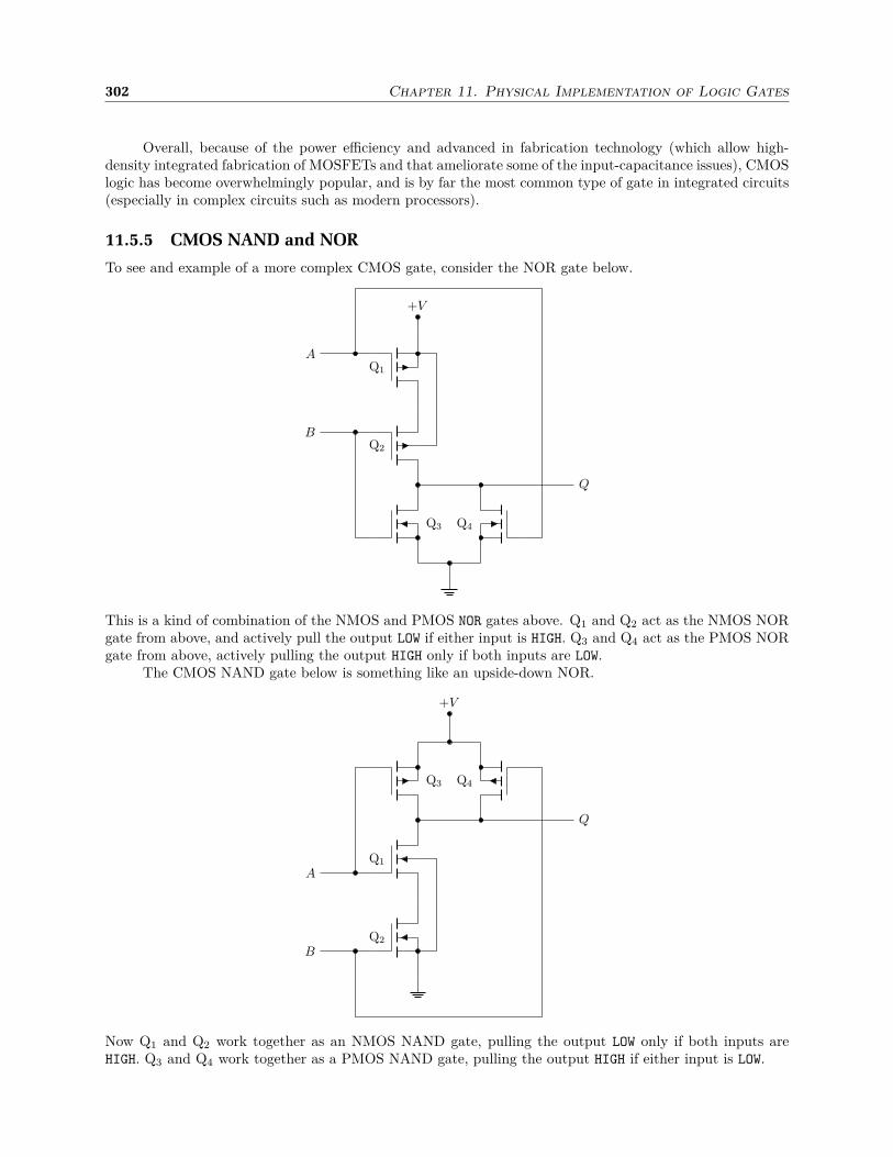
302 Chapter 11. Physical Implementation of Logic Gates
Overall, because of the power efficiency and advanced in fabrication technology (which allow high-density integrated fabrication of MOSFETs and that ameliorate some of the input-capacitance issues), CMOSlogic has become overwhelmingly popular, and is by far the most common type of gate in integrated circuits(especially in complex circuits such as modern processors).
11.5.5 CMOS NAND and NOR
To see and example of a more complex CMOS gate, consider the NOR gate below.
Q1
Q2
Q3 Q4
+V
A
B
Q
This is a kind of combination of the NMOS and PMOS NOR gates above. Q1 and Q2 act as the NMOS NORgate from above, and actively pull the output LOW if either input is HIGH. Q3 and Q4 act as the PMOS NORgate from above, actively pulling the output HIGH only if both inputs are LOW.
The CMOS NAND gate below is something like an upside-down NOR.
Q1
Q2
Q3 Q4
+V
A
B
Q
Now Q1 and Q2 work together as an NMOS NAND gate, pulling the output LOW only if both inputs areHIGH. Q3 and Q4 work together as a PMOS NAND gate, pulling the output HIGH if either input is LOW.
11.6 Circuit Practice 303
The designs here are relatively simple, reference versions of the gates. The “production” gates discussedin the next section typically had a more complex design to improve speed and output driving capability.
11.5.6 CMOS Nomenclature
To continue the discussion of TTL nomenclature from Section 11.4.1, we can now discuss some commonlyavailable CMOS devices. Again, an important side effect of CMOS designs is that they dissipate current whileswitching states, but not when “holding.” This feature makes CMOS generally power-efficient compared toTTL, and CMOS circuits take negligible steady-state input current (but of course are more susceptible tostatic discharge, which damages the oxide insulating layers of MOSFETs). CMOS devices are more flexiblein terms of logic level, and can operate at HIGH voltages other than +5 V. There are separate CMOS logicfamilies, but there are also CMOS variations of standard 74XX devices. For example, some flavors are:
• C: (e.g., 74CXX) operates from +3 to +15 V (compared to +5 V for standard TTL, which typicallytranslates to an acceptable range of +4.5 to +5.5), with a nominal “trigger” range arranged symmet-rically about 1⁄2 of the supply voltage. More specifically, for example, at a supply of +10 V, an inputbelow 2 V is recognized (guaranteed) as LOW, and an input above 8 V is recognized as HIGH. The outputcurrent at a supply voltage of 5 V is ±1.75 mA for the 74C00. (Compare this to the ability of the 7400to sink 16 mA with a LOW output, but a much weaker current driving ability with a HIGH output.)
• HC: high-speed CMOS, operates from a supply of +2 to +6 V; at a supply of +6 V, an input below1.8 V is recognized as LOW, and an input above 4.2 V is recognized as HIGH. The output current driveis equivalent to the 74CXX series at +5 V supply voltage.
• HCT: high-speed, compatible levels with TTL (+5 V, and a trigger-voltage range that matches theTTL specification).
• AC, ACT: advanced (i.e., fast) CMOS, ACT is the advanced HCT.
Another classic CMOS line of ICs is the 40XX-series family, which was historically important and stillavailable now. This family is named more simply, so that for example a 4001 is a quad 2-input NOR, a4011 is a quad 2-input NAND, and so on. The 4-digit part number is preceded by a short, manufacturerspecific code (so that the CD4011 was manufactured by Intersil, whereas the MC4011 was by Mororola, ornow ON Semiconductor). The 40XX series had the weak output-drive capability that we noted before (at a5-V supply the output could drive about ±1 mA, but increasing to ±7 mA at a 15-V supply). For example,one of these CMOS chips can drive a low-power TTL gate (74LXX), but driving a regular TTL gate (74XX)is more complicated, and may or may not be feasible depending on the exact chips involved.
11.6 Circuit Practice
11.6.1 Mystery RTL/DL Gate
To practice BJT/diode-based logic gates, consider the circuit below. What kind of gate is this?

304 Chapter 11. Physical Implementation of Logic Gates
A
B
Q
+5 V
Solution. Due to the arrangement of diodes, the only way to turn the transistor ON is to have one inputHIGH and one LOW. In this case, the output is LOW; otherwise the output is HIGH. Thus, this is an XNOR gate.
11.6.2 CMOS Level-Shifting Buffers
Shown below are two level-shifting buffers—they take in logic at nominal level +VDD and output logicat nominal level +VCC. (These circuits only handle “high–to–low” conversion, where VDD ≥ VCC, which isuseful, for example, in converting high-level CMOS signals to TTL.) One of them is a simple buffer, whilethe other acts as an inverter. The points of this exercise is to verify that the circuits work as advertised, andto figure out which is the buffer and which is the inverter.
A
+VDD +VCC
Q
Q1
Q2
Q3
Q4
Q5
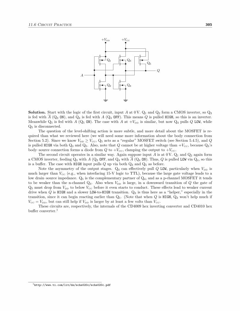
11.6 Circuit Practice 305
A
+VDD +VCC
Q
Q1
Q2
Q3
Q4
Q5
Solution. Start with the logic of the first circuit, input A at 0 V. Q1 and Q2 form a CMOS inverter, so Q3
is fed with A (Q3 ON), and Q4 is fed with A (Q4 OFF). This means Q is pulled HIGH, so this is an inverter.Meanwhile Q5 is fed with A (Q5 ON). The case with A at +VDD is similar, but now Q4 pulls Q LOW, whileQ5 is disconnected.
The question of the level-shifting action is more subtle, and more detail about the MOSFET is re-quired than what we reviewed here (we will need some more information about the body connection fromSection 5.2). Since we know VDD ≥ VCC, Q5 acts as a “regular” MOSFET switch (see Section 5.4.5), and Qis pulled HIGH via both Q3 and Q5. Also, note that Q cannot be at higher voltage than +VCC, because Q3’sbody–source connection forms a diode from Q to +VCC, clamping the output to +VCC.
The second circuit operates in a similar way. Again suppose input A is at 0 V. Q1 and Q2 again forma CMOS inverter, feeding Q3 with A (Q3 OFF, and Q4 with A (Q4 ON). Thus, Q is pulled LOW via Q4, so thisis a buffer. The case with HIGH input pulls Q up via both Q3 and Q5 as before.
Note the asymmetry of the output stages. Q4 can effectively pull Q LOW, particularly when VDD ismuch larger than VCC (e.g., when interfacing 15-V logic to TTL), because the large gate voltage leads to alow drain–source impedance. Q5 is the complementary partner of Q4, and as a p-channel MOSFET it tendsto be weaker than the n-channel Q4. Also when VDD is large, in a downward transition of Q the gate ofQ5 must drop from VDD to below VCC before it even starts to conduct. These effects lead to weaker currentdrive when Q is HIGH and a slower LOW-to-HIGH transition. Q3 is thus here as a “helper,” especially in thetransition, since it can begin reacting earlier than Q5. (Note that when Q is HIGH, Q3 won’t help much ifVCC = VDD, but can still help if VDD is larger by at least a few volts than VCC.
These circuits are, respectively, the internals of the CD4009 hex inverting converter and CD4010 hexbuffer converter.1
1http://www.ti.com/lit/ds/schs020c/schs020c.pdf
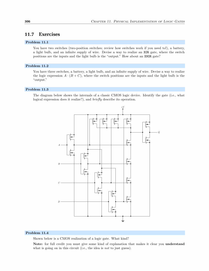
306 Chapter 11. Physical Implementation of Logic Gates
11.7 Exercises
Problem 11.1
You have two switches (two-position switches; review how switches work if you need to!), a battery,a light bulb, and an infinite supply of wire. Devise a way to realize an XOR gate, where the switchpositions are the inputs and the light bulb is the “output.” How about an XNOR gate?
Problem 11.2
You have three switches, a battery, a light bulb, and an infinite supply of wire. Devise a way to realizethe logic expression A · (B + C), where the switch positions are the inputs and the light bulb is the“output.”
Problem 11.3
The diagram below shows the internals of a classic CMOS logic device. Identify the gate (i.e., whatlogical expression does it realize?), and briefly describe its operation.
+V
A
B
C
D
Q
Problem 11.4
Shown below is a CMOS realization of a logic gate. What kind?
Note: for full credit you must give some kind of explanation that makes it clear you understandwhat is going on in this circuit (i.e., the idea is not to just guess).
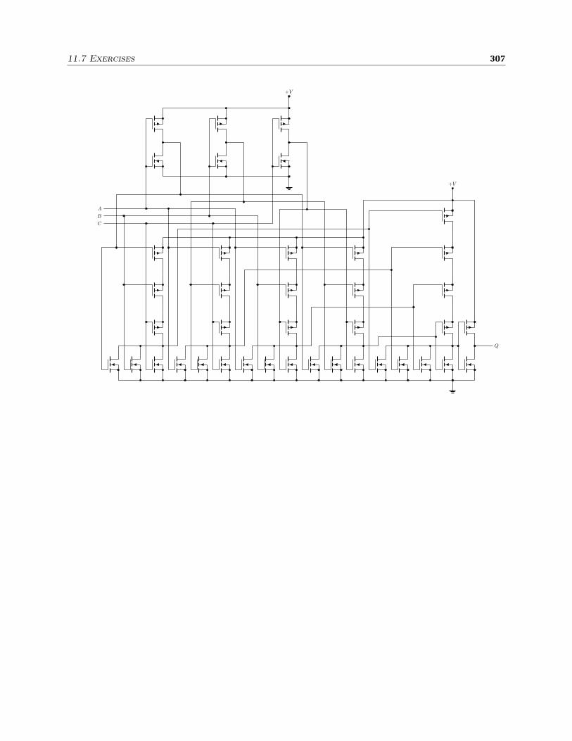
11.7 Exercises 307
+V
+V
A
B
C
Q


Chapter 12
Multiplexers and Demultiplexers
12.1 Multiplexers
Simply put, a digital multiplexer (or MUX for short) is a logic device that maps one of many (digital)inputs to one (digital) output. You select which input to connect to the output using the “address” inputs.The multiplexer is the logic analog of a many-to-one mechanical rotary switch.
Multiplexers are useful devices. For example, you can use them to “pack” data from multiple sources(“parallel data”) onto a single “serial” transmission line (e.g., for phone or computer networks). They canalso be used to sample or “poll” data from multiple sources, and ultimately allow scaling of many digitaldevices into modern computers. Multiplexers are examples of MSI (medium-scale integration) devices,“medium-scale” here meaning dozens of gates on 1 chip.
12.1.1 Example: 74151
An example of a multiplexer is the 74151 (which for example, with manufacturer and TTL-flavor codeswould be something more like DM74LS151), an 8-input MUX, shown schematically below.
74151
EA2
A1
A0
I7
I6
I5
I4
I3
I2
I1
I0
Q
Q
There are a number of features here:
• I0–I7 are the 8 inputs.
• A0–A2 are the 3 address lines, to select among the 23 = 8 inputs; the idea is to select input n bysetting A2A1A0 to n in binary.
• Q is the output: the selected input is copied to the output.
• Q is an inverted copy of the output.
• E or ENABLE (read this as “enable LOW”; this input is also called “STROBE” in the data sheet1) is a “chip
1http://www.ti.com/lit/ds/symlink/sn74ls151.pdf

310 Chapter 12. Multiplexers and Demultiplexers
enable” line. If E is LOW, the chip works as we have described; if E is HIGH, then Q = LOW Q = HIGH,independent of the states of I0−7 and A0−2.
Another example of a common MUX is the 74150, a 16-input MUX (with 4-bit address).
12.2 Demultiplexers
A demultiplexer (or DEMUX for short) is the “opposite” of the MUX, in the sense that a single inputis copied to a selected one of many possible outputs. Again, these are useful in, for example, packing andunpacking data to and from a transmission line via a MUX–DEMUX pair. Also a variation on the DEMUXis a decoder, which is the same as a DEMUX, but only selects the output, without copying any input (the“data” is effectively constant HIGH).
12.2.1 Example: 74138
A good DEMUX example is the 74138, a 1-to-8 DEMUX, as shown below.
74138
E3
E2
E1
A2
A1
A0
O7
O6
O5
O4
O3
O2
O1
O0
To go over the features here:
• O0–O7 are the 8 outputs, Note that they are inverted (i.e., their “normal,” unselected state is HIGH).
• A0–A2 are the 3 address lines, again to select among the 23 = 8 inputs in the same way as the MUX.
• E1, E2, and and E3 are chip-enable inputs. The chip is enabled if E1 = E2 = LOW and E3 = HIGH.Then the operation is as follows.
– If the chip is enabled, then the selected output Oj is LOW. (The others are HIGH.) In this case, thechip acts as a decoder.
– If the chip is not enabled, then all outputs Oj are HIGH.
– To operate this chip as a DEMUX instead of just a decoder, use E1 or E2 as a data input. Inthis case, the selected output copies E1 or E2, while the others remain HIGH. Alternately, E3 canwork as a data input, in which case the selected output copies E3 (with the others still HIGH).
Another example of a common MUX is the 74154, a 16-output decoder/DEMUX (with 4-bit address).
12.3 Making a MUX
The logic underlying a multiplexer is not difficult to understand. There are two basic elements: a decoderand “routing” logic. As an example, let’s consider an 8-input multiplexer. The decoder, as we described,takes address inputs A0–A2, and sets the corresponding one of 8 outputs C0–C7 HIGH, with the others LOW.We can simply use AND gates to set each output when matching the correct address combination, as below.

12.4 Expanding a MUX (or DEMUX) 311
A2A1A0
C0 C1 C2
· · ·
To be more efficient in terms of gates, we would only use one NOT gate for each of A0, A1, and A2, ratherthan NOT gates as shown, but the input NOT operations simplify the diagram.
The routing logic then has the algebraic form
Q = (C0I0 + C1I2 + · · · )E, (12.1)
if we include an ENABLE input. Notice that the E is negated twice, which means we’re negating the “E”input—the chip should be active when E is LOW, so we should AND the output with the negation of this (sowe do an AND with 1, copying the input to the output). Of course we could just write this as an E, but thisemphasizes the enable-LOW function of this variable.
The above expression means that the disabled output state is LOW; this is how the 74151 works. Youcould also imagine a MUX in which the disabled state is HIGH, in which case
Q = (C0I0 + C1I2 + · · · ) + E (12.2)
is the appropriate expression. In the disabled state E is HIGH, forcing Q to be the same.
12.4 Expanding a MUX (or DEMUX)
A useful technique is to combine MUXs into larger MUXs. For example given, 8× 8-input MUXs, how dowe make a 64-input MUX? This shows the real idea behind having chip-enable inputs: we will use the Einputs and an 8-output decoder, as shown below.
74151 74151
74138
A2
A1
A0
A0 A1 A2
A3 A4 A5
O0 O1 O2 O3 O4 O5 O6 O7
I0 I1 I2 I3 I4 I5 I6 I7 A0 A1 A2 E
I0–I7 I8–I15
Q
I0 I1 I2 I3 I4 I5 I6 I7 A0 A1 A2 E
Q
· · · etc.
One detail that we have left out is that the Q outputs must be combined by an OR gate. An importantalternative is to use chips with three-state logic. For these chips, the output is disconnected (high-impedance) when the chip is not enabled. In this case, you can just connect the chip outputs directlytogether, since only one chip will be enabled at a time. In this example, we can use the three-state alternative74251 instead of the 74151.
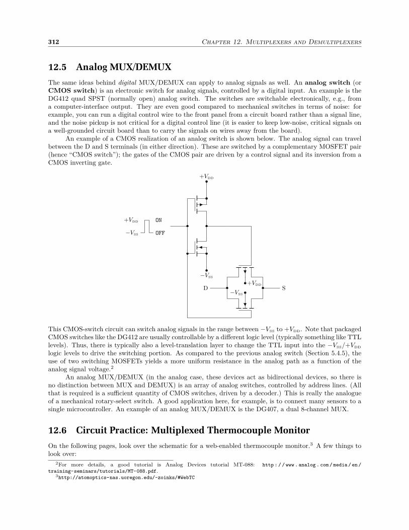
312 Chapter 12. Multiplexers and Demultiplexers
12.5 Analog MUX/DEMUX
The same ideas behind digital MUX/DEMUX can apply to analog signals as well. An analog switch (orCMOS switch) is an electronic switch for analog signals, controlled by a digital input. An example is theDG412 quad SPST (normally open) analog switch. The switches are switchable electronically, e.g., froma computer-interface output. They are even good compared to mechanical switches in terms of noise: forexample, you can run a digital control wire to the front panel from a circuit board rather than a signal line,and the noise pickup is not critical for a digital control line (it is easier to keep low-noise, critical signals ona well-grounded circuit board than to carry the signals on wires away from the board).
An example of a CMOS realization of an analog switch is shown below. The analog signal can travelbetween the D and S terminals (in either direction). These are switched by a complementary MOSFET pair(hence “CMOS switch”); the gates of the CMOS pair are driven by a control signal and its inversion from aCMOS inverting gate.
−VSS
+VDD
+VDD
−VSS OFF
ON
D S+VDD
−VSS
This CMOS-switch circuit can switch analog signals in the range between −VSS to +VDD. Note that packagedCMOS switches like the DG412 are usually controllable by a different logic level (typically something like TTLlevels). Thus, there is typically also a level-translation layer to change the TTL input into the −VSS/+VDD
logic levels to drive the switching portion. As compared to the previous analog switch (Section 5.4.5), theuse of two switching MOSFETs yields a more uniform resistance in the analog path as a function of theanalog signal voltage.2
An analog MUX/DEMUX (in the analog case, these devices act as bidirectional devices, so there isno distinction between MUX and DEMUX) is an array of analog switches, controlled by address lines. (Allthat is required is a sufficient quantity of CMOS switches, driven by a decoder.) This is really the analogueof a mechanical rotary-select switch. A good application here, for example, is to connect many sensors to asingle microcontroller. An example of an analog MUX/DEMUX is the DG407, a dual 8-channel MUX.
12.6 Circuit Practice: Multiplexed Thermocouple Monitor
On the following pages, look over the schematic for a web-enabled thermocouple monitor.3 A few things tolook over:
2For more details, a good tutorial is Analog Devices tutorial MT-088: http : / / www . analog . com / media / en /
training-seminars/tutorials/MT-088.pdf.3http://atomoptics-nas.uoregon.edu/~zoinks/#WebTC

12.6 Circuit Practice: Multiplexed Thermocouple Monitor 313
• There are provisions for 8 thermocouple inputs.
• The thermocouples are monitored by the AD594, which provides “ice point” compensation and buffersthe thermocouple signal. However, this is a relatively expensive chip, so rather than having one foreach thermocouple, we just use an analog multiplexer (IC1).
• The output is converted to digital via an analog-to-digital converter (IC3).
• The multiplexer address is controlled by an Ethernut microcontroller, which also reads out the ADC.The Ethernut has an ethernet port, and thus has firmware to make a web site to display the tempera-tures. It also controls an LCD display on the actual box.

314 Chapter 12. Multiplexers and Demultiplexers
WE
B-E
NA
BL
ED
TH
ER
MO
CO
UP
LE
RE
AD
OU
T -
- 1
D. A
. ST
EC
K, P
.GA
SK
EL
LR
ev. D
4/
18/
09
14
IC2
AD
594
1
-
+
2 3 4 5 6 7
13 12 11 10 9 8
-
+
V-
-TC
+TC ice
po
int
com
p+
V+
+A
GG
overloaddetect
-IN
+IN
-AL
M
+A
LM
CO
MP
VO FB
-C-TCOM+T
+C
+
IC1
DG
407
1 2 3 4 5 6 7 8 9 10 11 12 13 14
28 27 26 25 24 23 22 21 20 19 18 17 16 15
dec
od
ers/
dri
ver
s
V+
V-
EN
A2
A1
A0
+ + + + + + +
J8 J7 J6 J5 J4 J3 J2 J1
+V
A
+V
A
16
IC3
AD
C12
130
1 2 3 4 5 6 7
15 14 13 12 11 10
89
CH
0
CH
1
CO
M
DO
R
EO
C
V
-
V
+
DG
ND
V +
CC
LK
SC
LK DI
DO CS
CO
NV
V +
RE
F
RE
F
D A+
VA
14
IC5
EC
S-10
0A-0
50
1 78
NC
GN
D
V+
OU
T
+V
D
5 M
Hz
IC4
LM
4040
-5.0
R2
1 kΩ
+V
A +5V
46P
E7
45 44 43 42 41 40 39
PE
6
PE
5
PE
4
PE
3
PE
2
PE
1
PE
0
PO
RT
D: I
NP
UT
54P
B7
53 52 51 50 49 48 47
PB
6
PB
5
PB
4
PB
3
PB
2
PB
1
PB
0
PO
RT
B: O
UT
PU
T
PO
RT
E: I
NP
UT
ET
HE
RN
UT
2.
0 R
EV
A /
2.1
RE
V B
EX
PA
NSI
ON
PO
RT
62P
D7
61 60 59 58 57 56 55
PD
6
PD
5
PD
4
PD
3
PD
2
PD
1
PD
0
PO
RT
D: O
UT
PU
T
1,14
2,13
6,9
7,8
16
LC
D1
DM
C20
261N
Y-L
Y-A
XE
1 2 3 4 5 6 7
15 14 13 12 11 10
89
V V V RS
R/
W
E DB
0
DB
1
LE
D -
LE
D+
DB
7
DB
6
DB
5
DB
4
DB
3
DB
2
SS DD
EE
RL
1W
107D
IP-1
K1
20 kΩ
+V
D
con
tras
tad
j.+
VD
R3
8.2 Ω
5 W
J-ty
pe
ther
mo
cou
ple
con
nec
tors
AL
AR
M
PE
0, P
E1:
res
erv
ed f
or
UA
RT
0/R
S23
2 (
for
deb
ug
gin
g)
PE
5: r
eser
ved
fo
r e
ther
net
in
terr
up
t
R1
20 kΩ
+V
D
IC6
DG
412L
1 2 3 4 5 6 7 8
16 15 14 13 12 11 10 9
V+
V-
GN
DV
L
4xSP
STN
.O.
+V
A
+V
A+
VA
PE
7: c
on
fig
ure
as
ou
tpu
t
+V
A
PB
4 re
serv
ed f
or
Fla
sh M
em+
VA

12.6 Circuit Practice: Multiplexed Thermocouple Monitor 315
+V
(+
V
)A
RE
F
+
C16
10 µ
FC
170.
1 µ
F
PP
PO
OO
WW
WE
EE
RR
R S
SSUU
UP
PP
PP
PL
LL
YY
Y A
AA
NN
ND
DD
RR
RE
EE
FF
FE
EE
RR
RE
EE
NN
NC
CC
EE
E B
BB
YY
YP
PP
AA
ASS
SSSSIIINN
NG
GG
(((II
ICC
C11
1---IIICC
C44
4)))
+V
D
C18
0.01
µF
TO
IC
+
C4-
C7
10 µ
FC
8-C
110.
1 µ
FC
12-C
150.
01 µ
F
TO
IC
WE
B-E
NA
BL
ED
TH
ER
MO
CO
UP
LE
RE
AD
OU
T -
- 2
12V
CC
5
11 10 9 8 7 6 5
DC
RE
SE
T/
GN
DET
HE
RN
UT
2.0
RE
V A
EX
PA
NSI
ON
PO
RT
+ -
~~
BR
1M
B2S
1 3 2
J92.
1 m
m p
ow
er(r
igh
t an
gle
)
D1
P6K
E15
CA
F1
1 A
9 V
, 750
mA
PO
WE
R I
N(p
ola
rity
no
t im
po
rtan
t)
IC7
LM
1086
-AD
J
IN
AD
J
OU
T
K2
100 Ω
R4
121 Ω
R5
330 Ω
+
C1
22 µ
F
+
C3
22 µ
F
+
C2
22 µ
F
+V
A
+V
D
4V
CC
5
3 2V
CC
3
1
VC
C5
GN
D
GN
D
GN
D
VC
C3
VC
C5
sin
gle
co
nn
ecti
on
bet
wee
n a
nal
og
an
dd
igit
al g
rou
nd
pla
nes
adju
st f
or
5.1-
5.2
V
PP
PO
OO
WW
WE
EE
RR
R S
SSUU
UP
PP
PP
PL
LL
YY
Y B
BB
YY
YP
PP
AA
ASS
SSSSIIINN
NG
GG
(((II
ICC
C66
6)))
+V
A
C19
0.1
µF
TO
IC
anal
og
gro
un
dd
igit
al g
rou
nd
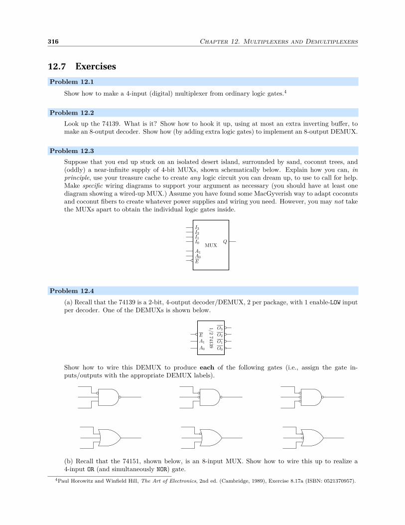
316 Chapter 12. Multiplexers and Demultiplexers
12.7 Exercises
Problem 12.1
Show how to make a 4-input (digital) multiplexer from ordinary logic gates.4
Problem 12.2
Look up the 74139. What is it? Show how to hook it up, using at most an extra inverting buffer, tomake an 8-output decoder. Show how (by adding extra logic gates) to implement an 8-output DEMUX.
Problem 12.3
Suppose that you end up stuck on an isolated desert island, surrounded by sand, coconut trees, and(oddly) a near-infinite supply of 4-bit MUXs, shown schematically below. Explain how you can, in
principle, use your treasure cache to create any logic circuit you can dream up, to use to call for help.Make specific wiring diagrams to support your argument as necessary (you should have at least onediagram showing a wired-up MUX.) Assume you have found some MacGyverish way to adapt coconutsand coconut fibers to create whatever power supplies and wiring you need. However, you may not takethe MUXs apart to obtain the individual logic gates inside.
MUX
EA0
A1
I0
I1
I2
I3
Q
Problem 12.4
(a) Recall that the 74139 is a 2-bit, 4-output decoder/DEMUX, 2 per package, with 1 enable-LOW inputper decoder. One of the DEMUXs is shown below.
1/274139
O3
O2
O1
O0
EA1
A0
Show how to wire this DEMUX to produce each of the following gates (i.e., assign the gate in-puts/outputs with the appropriate DEMUX labels).
(b) Recall that the 74151, shown below, is an 8-input MUX. Show how to wire this up to realize a4-input OR (and simultaneously NOR) gate.
4Paul Horowitz and Winfield Hill, The Art of Electronics, 2nd ed. (Cambridge, 1989), Exercise 8.17a (ISBN: 0521370957).

12.7 Exercises 317
74151
EA2
A1
A0
I7
I6
I5
I4
I3
I2
I1
I0
Q
Q

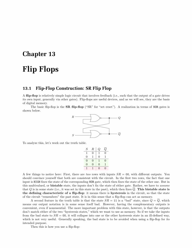
Chapter 13
Flip Flops
13.1 Flip-Flop Construction: SR Flip Flop
A flip-flop is relatively simple logic circuit that involves feedback (i.e., such that the output of a gate drivesits own input, generally via other gates). Flip-flops are useful devices, and as we will see, they are the basisof digital memory.
The basic flip-flop is the SR flip-flop (“SR” for “set–reset”). A realization in terms of NOR gates isshown below.
R
S
Q
Q
To analyze this, let’s work out the truth table.
S R Q Q1 0 1 00 1 0 10 0 1 00 0 0 11 1 0 0
A few things to notice here: First, there are two rows with inputs SR = 00, with different outputs. Youshould convince yourself that both are consistent with the circuit. In the first two rows, the fact that oneinput is HIGH fixes the state of the corresponding NOR gate, which then fixes the state of the other one. But inthis multivalued, or bistable state, the inputs don’t fix the state of either gate. Rather, we have to assume
that Q is in some state (i.e., it was set in this state in the past), which then fixes Q. This bistable state isthe defining characteristic of a flip-flop: it means there is hysteresis in the circuit, so that the stateof the circuit “remembers” the past state. It is in this sense that a flip-flop can act as memory.
A second feature in the truth table is that the state SR = 11 is a “bad” state, since Q = Q, whichmeans our output notation is in some sense itself bad. However, having the complementary outputs isconvenient, even if nonessential. The more important problem with this state, however, is that the outputsdon’t match either of the two “hysteresis states,” which we want to use as memory. So if we take the inputsfrom the bad state to SR = 00, it will collapse into one or the other hysteresis state in an ill-defined way,which is not very useful. Generally speaking, the bad state is to be avoided when using a flip-flop for itsintended purpose.
Then this is how you use a flip-flop:

320 Chapter 13. Flip Flops
• The inputs R and S are normally 0 (i.e., the flip-flop is in one of the memory states).
• Bringing S to 1 and back to 0 (the “set” operation) changes Q = 1 and Q = 0. This state is“remembered” when R = S = 0.
• Bringing R to 1 and back to 0 (the “reset” operation) changes Q = 0 and Q = 1. This state is“remembered” when R = S = 0.
13.1.1 Application: Debounced Switch
A simple application of the SR flip-flop is to make a debounced switch. Recall that switches are mechanicaldevices that make and break electrical connections. We can use a switch as in the schematic below to togglebetween TTL HIGH and LOW.
1 kΩ
+5 V
openswitch
closeswitch
That is, if the switch is open, the output is pulled up by the resistor to +5 V, while a closed switch correspondsto a 0-V output.
The problem is that the output will really look like the output shown for one open/close cycle. Whenwe open the switch, the output goes HIGH with no problem, because the switch cleanly breaks the connection.However, when closing the switch, there is a problem. The contacts must close, and normally they are heldtogether by some spring pressure. But when they close, one contact smacks into the other and “bounces”off of it, just like dropping a chunk of metal on a hard floor. The spring action pushes the contacts togetheragain, and the result is a few extra, short pulses due to the switch bounce, typically on ms time scales.1 Thisis a real problem, for example, if the pulse is to drive the input of a counter. For example, the switch couldbe actuated by items on a manufacturing line, to count the number of items produced; it would obviouslynot be a very good count if there were several extra bounces for each item to count.
A simple solution to this uses a flip-flop and a slightly more complicated switch. Before getting tothat, let’s introduce a functionally equivalent variant of the above RS flip-flop, now based on NAND gates.
Q
Q
S
R
The operation is the same as before, but note the inputs are R and S, so their senses are inverted. That is,the “usual” input state should be R = S = 1. Then you bring S momentarily to 0 to set the flip-flop (i.e.,Q = 1), and you bring R momentarily to 0 to reset it (Q = 0). We will leave the analysis of this flip-flop asa circuit-practice exercise.
Now the debounced switch uses an SPDT switch (the “bouncy” switch used an SPST switch). The“up” switch state sets Q = 1, and the “down” switch state sets Q = 0.
1example: http://www.maximintegrated.com/en/app-notes/index.mvp/id/287

13.2 Clocked Flip-Flops 321
Q
1 kΩ
1 kΩ
+5 V
+5 V
Q = 1
Q = 0
S
R
During a bounce, the switch makes no connection to either contact, so both S and R are 1. This is thememory state, so the flip-flop holds the last switch state, which persists through the duration of the bouncing.
13.2 Clocked Flip-Flops
An important class of flip-flops, one step up in sophistication from the basic flip-flops above, is that ofclocked flip-flops. A clock is an external, typically periodic logic signal that synchronizes signals incomplex circuits. We will see some examples later, but in complex circuits, this synchronization is importantin avoiding problems with race conditions. The idea in a clocked flip-flop is that the input datum is onlyaccepted during a particular phase of the clock cycle, for example when the clock is HIGH. The clock thenfunctions as a “gate” for the input data. An example of a clocked SR flip-flop is shown below.
Q
Q
S
R
CLK
S
R
Note that when the CLK signal is LOW, this guarantees that the flip-flop is in the memory state. We can writethe truth table for this circuit as follows.
S R Qn+1
0 0 Qn
1 0 10 1 01 1 “bad”
Here, Qn is the output state after the nth pulse. If S and R are LOW, then the flip-flop stays in the memorystate, and the state Qn persists to the next clock cycle. Otherwise, the clocking NAND gates act as invertersfor the S and R inputs, so the inputs set and reset as usual (with momentary HIGH action), but only whenthe clock is HIGH.
13.2.1 D-Type Flip-Flop
An important class of clocked flip-flop is the D-type flip-flop, which is basically the clocked SR flip-flop,but where the two inputs are always in opposite states, as shown below. Here, the D or “data” input drivesthe S and R inputs oppositely.
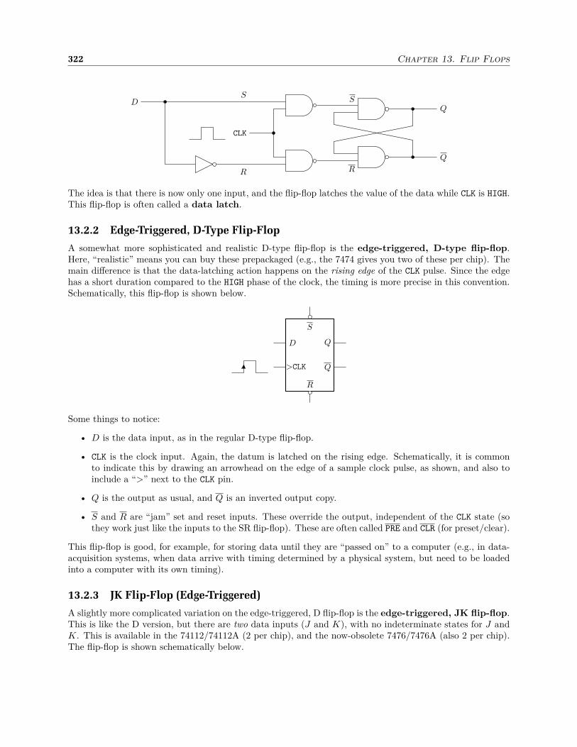
322 Chapter 13. Flip Flops
Q
Q
S
R
CLK
S
R
D
The idea is that there is now only one input, and the flip-flop latches the value of the data while CLK is HIGH.This flip-flop is often called a data latch.
13.2.2 Edge-Triggered, D-Type Flip-Flop
A somewhat more sophisticated and realistic D-type flip-flop is the edge-triggered, D-type flip-flop.Here, “realistic” means you can buy these prepackaged (e.g., the 7474 gives you two of these per chip). Themain difference is that the data-latching action happens on the rising edge of the CLK pulse. Since the edgehas a short duration compared to the HIGH phase of the clock, the timing is more precise in this convention.Schematically, this flip-flop is shown below.
D
>CLK
Q
Q
R
S
Some things to notice:
• D is the data input, as in the regular D-type flip-flop.
• CLK is the clock input. Again, the datum is latched on the rising edge. Schematically, it is commonto indicate this by drawing an arrowhead on the edge of a sample clock pulse, as shown, and also toinclude a “>” next to the CLK pin.
• Q is the output as usual, and Q is an inverted output copy.
• S and R are “jam” set and reset inputs. These override the output, independent of the CLK state (sothey work just like the inputs to the SR flip-flop). These are often called PRE and CLR (for preset/clear).
This flip-flop is good, for example, for storing data until they are “passed on” to a computer (e.g., in data-acquisition systems, when data arrive with timing determined by a physical system, but need to be loadedinto a computer with its own timing).
13.2.3 JK Flip-Flop (Edge-Triggered)
A slightly more complicated variation on the edge-triggered, D flip-flop is the edge-triggered, JK flip-flop.This is like the D version, but there are two data inputs (J and K), with no indeterminate states for J andK. This is available in the 74112/74112A (2 per chip), and the now-obsolete 7476/7476A (also 2 per chip).The flip-flop is shown schematically below.

13.3 Counters 323
J
>CLK
K
Q
Q
R
S
The operation with the two new inputs is as follows.
• The CLK on this flip-flop, as drawn, triggers on the falling edge of the clock. Note the NOT circle onthe clock input, and the sample clock pulse. This is how the 74112/74112A and 7476A work (the plain7476 triggers on the positive edge). That is, this device is negative-edge triggered.
• If J = 0 and K = 0, then Q persists on the next CLK pulse.
• If J = 1 and K = 0, then Q = 1 on the next CLK pulse.
• If J = 0 and K = 1, then Q = 0 on the next CLK pulse.
• If J = 1 and K = 1, then Q inverts on the next CLK pulse (i.e., it “toggles”).
• S and R are still jam set and reset inputs.
13.3 Counters
One useful application of flip-flops is in realizing counters, which count input pulses by incrementing abinary output. The basic building block of a counter is the divide-by-2 counter, shown below in terms ofa D-type flip-flop.
D
>CLK
Q
QIN
OUT
The timing diagram for this circuit is shown below. Note that transitions happen on the rising edge of theinput (clock) pulses, and essentially the output is just toggling its output on each clock cycle. Hence theterm “divide-by-2,” since the output pulse train oscillates at half the frequency of the input clock. Morespecifically, the flip-flop loads D = Q to Q on each rising pulse-edge.
CLK/IN
OUT/Q
D/Q
Since the output is just toggling, recall that we can also make a JK flip-flop do this by tying both J and Kinputs HIGH, as shown below.
J
>CLK
K
Q
IN
OUT
+5 V
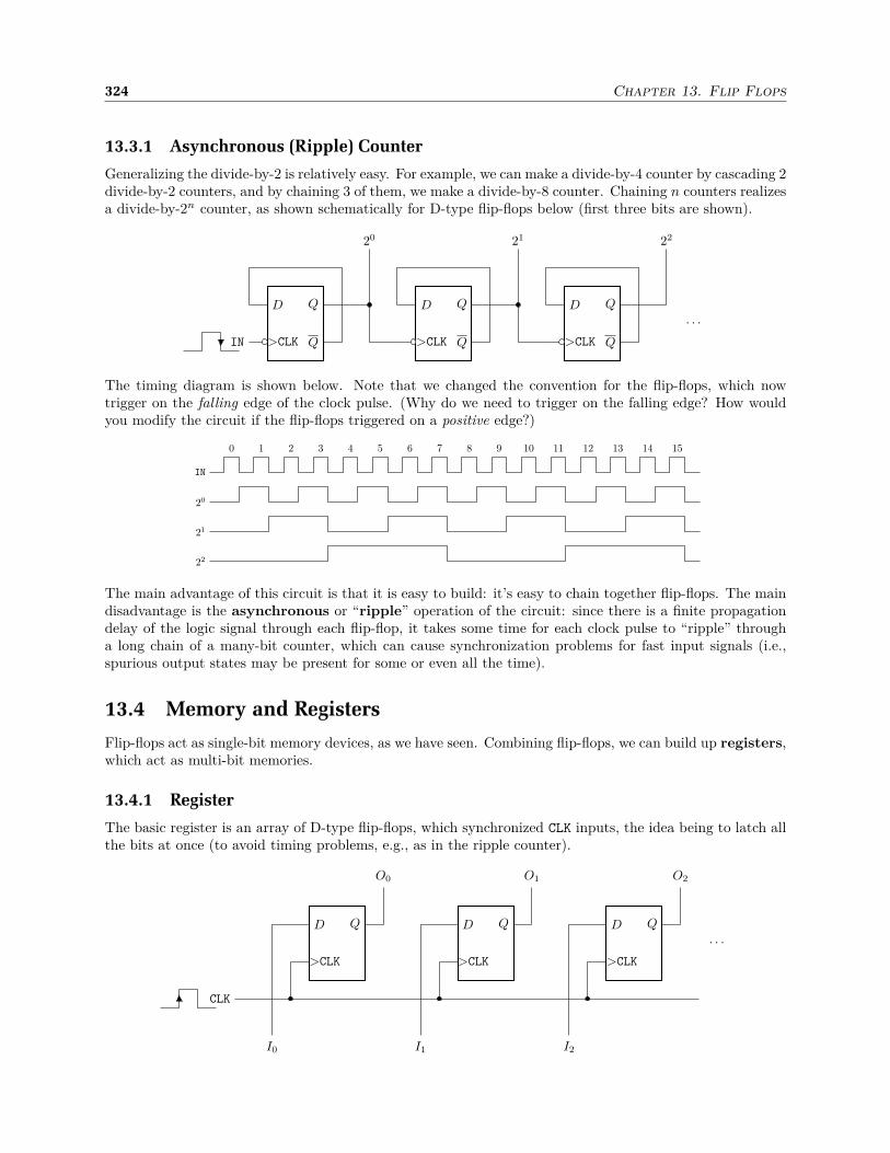
324 Chapter 13. Flip Flops
13.3.1 Asynchronous (Ripple) Counter
Generalizing the divide-by-2 is relatively easy. For example, we can make a divide-by-4 counter by cascading 2divide-by-2 counters, and by chaining 3 of them, we make a divide-by-8 counter. Chaining n counters realizesa divide-by-2n counter, as shown schematically for D-type flip-flops below (first three bits are shown).
D
>CLK
Q
QIN
20
D
>CLK
Q
Q
21
D
>CLK
Q
Q
22
· · ·
The timing diagram is shown below. Note that we changed the convention for the flip-flops, which nowtrigger on the falling edge of the clock pulse. (Why do we need to trigger on the falling edge? How wouldyou modify the circuit if the flip-flops triggered on a positive edge?)
0 1 2 3 4 5 6 7 8 9 10 11 12 13 14 15
IN
20
21
22
The main advantage of this circuit is that it is easy to build: it’s easy to chain together flip-flops. The maindisadvantage is the asynchronous or “ripple” operation of the circuit: since there is a finite propagationdelay of the logic signal through each flip-flop, it takes some time for each clock pulse to “ripple” througha long chain of a many-bit counter, which can cause synchronization problems for fast input signals (i.e.,spurious output states may be present for some or even all the time).
13.4 Memory and Registers
Flip-flops act as single-bit memory devices, as we have seen. Combining flip-flops, we can build up registers,which act as multi-bit memories.
13.4.1 Register
The basic register is an array of D-type flip-flops, which synchronized CLK inputs, the idea being to latch allthe bits at once (to avoid timing problems, e.g., as in the ripple counter).
D
>CLK
Q
CLK
I0
O0
D
>CLK
Q
I1
O1
D
>CLK
Q
I2
O2
· · ·
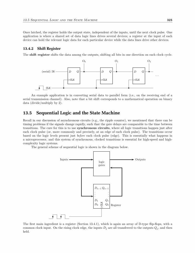
13.5 Sequential Logic and the State Machine 325
Once latched, the register holds the output state, independent of the inputs, until the next clock pulse. Oneapplication is where a shared set of data logic lines drives several devices; a register at the input of eachdevice can hold the relevant logic data for each particular device while the data lines drive other devices.
13.4.2 Shift Register
The shift register shifts the data among the outputs, shifting all bits in one direction on each clock cycle.
D
>CLK
Q
CLK
(serial) IN
O0
D
>CLK
Q
O1
D
>CLK
Q
O2
· · ·
An example application is in converting serial data to parallel form (i.e., on the receiving end of aserial transmission channel). Also, note that a bit shift corresponds to a mathematical operation on binarydata (divide/multiply by 2).
13.5 Sequential Logic and the State Machine
Recall in our discussion of asynchronous circuits (e.g., the ripple counter), we mentioned that there can betiming problems if the signals change rapidly, such that the gate delays are comparable to the time betweentransitions. The cure for this is to use synchronous circuits, where all logic transitions happen just aftereach clock pulse (or, more commonly and precisely, at an edge of each clock pulse). The transitions occurbased on the logic levels present just before each clock pulse (edge). This is essentially what happens ina microprocessor, and this system of synchronous, clocked transitions is essential for high-speed and high-complexity logic systems.
The general scheme of sequential logic is shown in the diagram below.
D0
D1
.
.
.
Dn−1
>CLK
Q0
Q1
.
.
.
Qn−1
logicgates
Register
Inputs Outputs
The first main ingredient is a register (Section 13.4.1), which is again an array of D-type flip-flops, with acommon clock input. On the rising clock edge, the inputs Dj are all transferred to the outputs Qj , and thenheld.
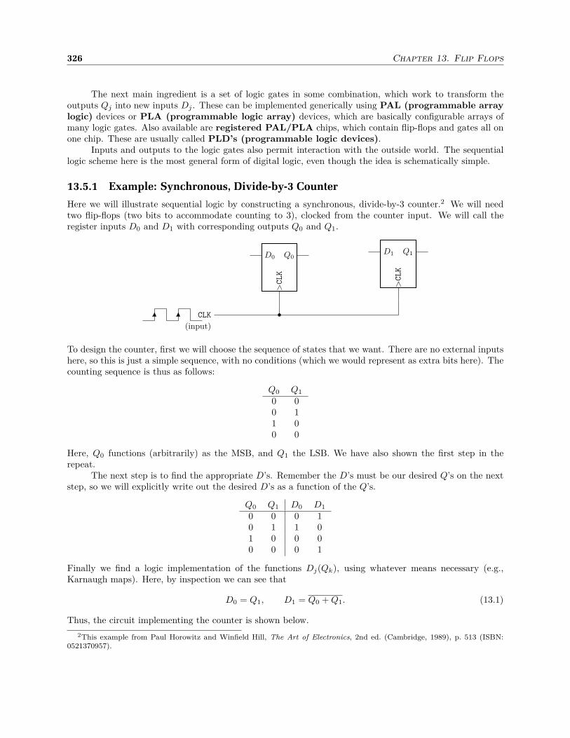
326 Chapter 13. Flip Flops
The next main ingredient is a set of logic gates in some combination, which work to transform theoutputs Qj into new inputs Dj . These can be implemented generically using PAL (programmable arraylogic) devices or PLA (programmable logic array) devices, which are basically configurable arrays ofmany logic gates. Also available are registered PAL/PLA chips, which contain flip-flops and gates all onone chip. These are usually called PLD’s (programmable logic devices).
Inputs and outputs to the logic gates also permit interaction with the outside world. The sequentiallogic scheme here is the most general form of digital logic, even though the idea is schematically simple.
13.5.1 Example: Synchronous, Divide-by-3 Counter
Here we will illustrate sequential logic by constructing a synchronous, divide-by-3 counter.2 We will needtwo flip-flops (two bits to accommodate counting to 3), clocked from the counter input. We will call theregister inputs D0 and D1 with corresponding outputs Q0 and Q1.
D0
>CLK
Q0
CLK
(input)
D1
>CLK
Q1
To design the counter, first we will choose the sequence of states that we want. There are no external inputshere, so this is just a simple sequence, with no conditions (which we would represent as extra bits here). Thecounting sequence is thus as follows:
Q0 Q1
0 00 11 00 0
Here, Q0 functions (arbitrarily) as the MSB, and Q1 the LSB. We have also shown the first step in therepeat.
The next step is to find the appropriate D’s. Remember the D’s must be our desired Q’s on the nextstep, so we will explicitly write out the desired D’s as a function of the Q’s.
Q0 Q1 D0 D1
0 0 0 10 1 1 01 0 0 00 0 0 1
Finally we find a logic implementation of the functions Dj(Qk), using whatever means necessary (e.g.,Karnaugh maps). Here, by inspection we can see that
D0 = Q1, D1 = Q0 + Q1. (13.1)
Thus, the circuit implementing the counter is shown below.
2This example from Paul Horowitz and Winfield Hill, The Art of Electronics, 2nd ed. (Cambridge, 1989), p. 513 (ISBN:0521370957).
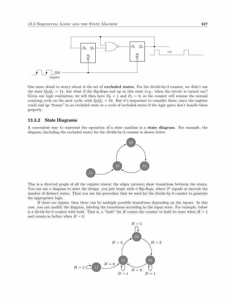
13.5 Sequential Logic and the State Machine 327
D0
>CLK
Q0
CLK
(input)
D1
>CLK
Q1
÷3
One more detail to worry about is the set of excluded states. For the divide-by-3 counter, we didn’t usethe state Q0Q1 = 11, but what if the flip-flops end up in this state (e.g., when the circuit is turned on)?Given our logic realization, we will then have D0 = 1 and D1 = 0, so the counter will resume the normalcounting cycle on the next cycle, with Q0Q1 = 10. But it’s important to consider these, since the registercould end up “frozen” in an excluded state or a cycle of excluded states if the logic gates don’t handle themproperly.
13.5.2 State Diagrams
A convenient way to represent the operation of a state machine is a state diagram. For example, thediagram (including the excluded state) for the divide-by-3 counter is shown below.
00
0110
11
This is a directed graph of all the register states; the edges (arrows) show transitions between the states.You can use a diagram to start the design: you just begin with n flip-flops, where 2n equals or exceeds thenumber of distinct states. Then you use the procedure that we used for the divide-by-3 counter to generatethe appropriate logic.
If there are inputs, then there can be multiple possible transitions depending on the inputs. In thiscase, you can modify the diagram, labeling the transitions according to the input state. For example, belowis a divide-by-3 counter with hold. That is, a “hold” bit H causes the counter to hold its state when H = 1
and counts as before when H = 0.
00
0110
11
H = 0
H = 0
H = 0
H = 0
H = 1
H = 1H = 1
H = 1
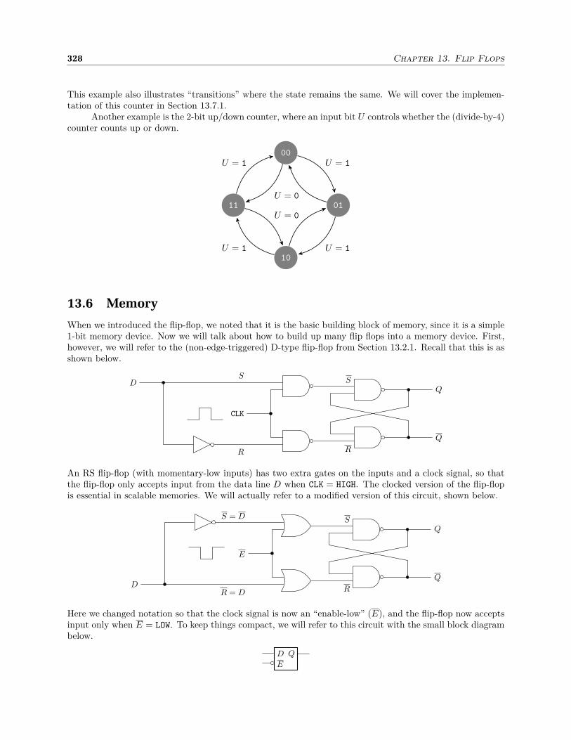
328 Chapter 13. Flip Flops
This example also illustrates “transitions” where the state remains the same. We will cover the implemen-tation of this counter in Section 13.7.1.
Another example is the 2-bit up/down counter, where an input bit U controls whether the (divide-by-4)counter counts up or down.
00
01
10
11
U = 1
U = 0
U = 1
U = 0
U = 1
U = 1
13.6 Memory
When we introduced the flip-flop, we noted that it is the basic building block of memory, since it is a simple1-bit memory device. Now we will talk about how to build up many flip flops into a memory device. First,however, we will refer to the (non-edge-triggered) D-type flip-flop from Section 13.2.1. Recall that this is asshown below.
Q
Q
S
R
CLK
S
R
D
An RS flip-flop (with momentary-low inputs) has two extra gates on the inputs and a clock signal, so thatthe flip-flop only accepts input from the data line D when CLK = HIGH. The clocked version of the flip-flopis essential in scalable memories. We will actually refer to a modified version of this circuit, shown below.
Q
Q
S
R
E
R = D
S = D
D
Here we changed notation so that the clock signal is now an “enable-low” (E), and the flip-flop now acceptsinput only when E = LOW. To keep things compact, we will refer to this circuit with the small block diagrambelow.
DE
Q
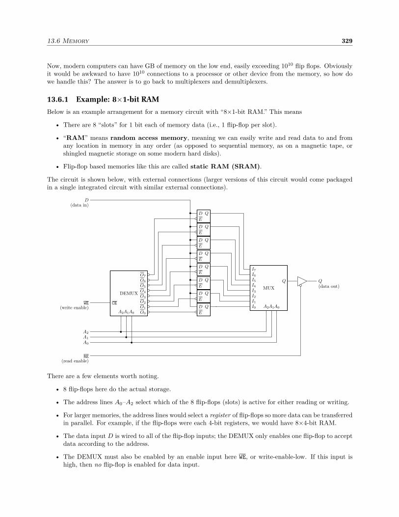
13.6 Memory 329
Now, modern computers can have GB of memory on the low end, easily exceeding 1010 flip flops. Obviouslyit would be awkward to have 1010 connections to a processor or other device from the memory, so how dowe handle this? The answer is to go back to multiplexers and demultiplexers.
13.6.1 Example: 8×1-bit RAMBelow is an example arrangement for a memory circuit with “8×1-bit RAM.” This means
• There are 8 “slots” for 1 bit each of memory data (i.e., 1 flip-flop per slot).
• “RAM” means random access memory, meaning we can easily write and read data to and fromany location in memory in any order (as opposed to sequential memory, as on a magnetic tape, orshingled magnetic storage on some modern hard disks).
• Flip-flop based memories like this are called static RAM (SRAM).
The circuit is shown below, with external connections (larger versions of this circuit would come packagedin a single integrated circuit with similar external connections).
DE
Q
DE
Q
DE
Q
DE
Q
DE
Q
DE
Q
DE
Q
DE
Q
DEMUX
O0
O1
O2
O3
O4
O5
O6
O7
CE
A0A1A2
MUX
I0
I1
I2
I3
I4
I5
I6
I7
A0A1A2
Q
A0
A1
A2
D(data in)
WE(write enable)
Q(data out)
RE(read enable)
There are a few elements worth noting.
• 8 flip-flops here do the actual storage.
• The address lines A0–A2 select which of the 8 flip-flops (slots) is active for either reading or writing.
• For larger memories, the address lines would select a register of flip-flops so more data can be transferredin parallel. For example, if the flip-flops were each 4-bit registers, we would have 8×4-bit RAM.
• The data input D is wired to all of the flip-flop inputs; the DEMUX only enables one flip-flop to acceptdata according to the address.
• The DEMUX must also be enabled by an enable input here WE, or write-enable-low. If this input ishigh, then no flip-flop is enabled for data input.
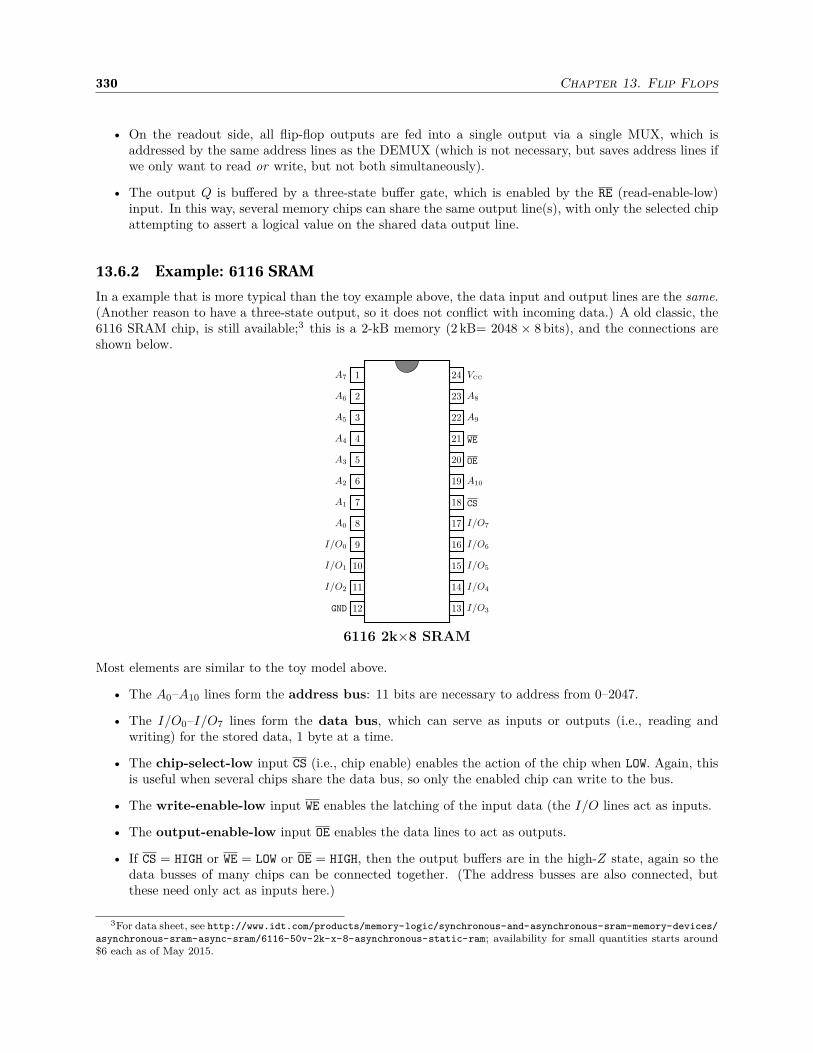
330 Chapter 13. Flip Flops
• On the readout side, all flip-flop outputs are fed into a single output via a single MUX, which isaddressed by the same address lines as the DEMUX (which is not necessary, but saves address lines ifwe only want to read or write, but not both simultaneously).
• The output Q is buffered by a three-state buffer gate, which is enabled by the RE (read-enable-low)input. In this way, several memory chips can share the same output line(s), with only the selected chipattempting to assert a logical value on the shared data output line.
13.6.2 Example: 6116 SRAM
In a example that is more typical than the toy example above, the data input and output lines are the same.(Another reason to have a three-state output, so it does not conflict with incoming data.) A old classic, the6116 SRAM chip, is still available;3 this is a 2-kB memory (2 kB= 2048 × 8 bits), and the connections areshown below.
12
11
10
9
8
7
6
5
4
3
2
1
13
14
15
16
17
18
19
20
21
22
23
24
GND
I/O2
I/O1
I/O0
A0
A1
A2
A3
A4
A5
A6
A7
I/O3
I/O4
I/O5
I/O6
I/O7
CS
A10
OE
WE
A9
A8
VCC
6116 2k×8 SRAM
Most elements are similar to the toy model above.
• The A0–A10 lines form the address bus: 11 bits are necessary to address from 0–2047.
• The I/O0–I/O7 lines form the data bus, which can serve as inputs or outputs (i.e., reading andwriting) for the stored data, 1 byte at a time.
• The chip-select-low input CS (i.e., chip enable) enables the action of the chip when LOW. Again, thisis useful when several chips share the data bus, so only the enabled chip can write to the bus.
• The write-enable-low input WE enables the latching of the input data (the I/O lines act as inputs.
• The output-enable-low input OE enables the data lines to act as outputs.
• If CS = HIGH or WE = LOW or OE = HIGH, then the output buffers are in the high-Z state, again so thedata busses of many chips can be connected together. (The address busses are also connected, butthese need only act as inputs here.)
3For data sheet, see http://www.idt.com/products/memory-logic/synchronous-and-asynchronous-sram-memory-devices/
asynchronous-sram-async-sram/6116-50v-2k-x-8-asynchronous-static-ram; availability for small quantities starts around$6 each as of May 2015.

13.7 State Machines with Memory 331
13.6.3 Other Memory Types
The SRAM above is the basic type of digital memory, but there are many other types. We will briefly reviewthem here.
• DRAM (dynamic RAM) uses a small capacitor to store a bit of information as a charge state.The disadvantage is that because the capacitor leaks, it must continually be “refreshed” (on ms timescales), which greatly complicates the overhead circuitry. The advantage is that DRAM is cheap andhighly scalable; DRAM is standard for large memory modules in modern computers.
• SRAM (static RAM) we have already talked about. Why do we want it? It is complicated tofabricate relative to DRAM, and is hard to scale to very large memory. However, it can be relativelypower efficient (no refreshing is necessary), and due to the lack of refreshing overhead, it can be mucheasier to use in small projects. Note that while no refresh is needed, SRAM is volatile (the storedinformation vanishes when the circuit is not powered).
• ROM (read-only memory) is not intended to be written, just read. The data are written duringmanufacturing.
• PROM (programmable ROM) is ROM that can be written (once!) using special programminghardware, which burns fused connections inside the chip by applying relatively high currents.
• EPROM (erasable PROM) is PROM that is programmed electronically, and the programming canbe erased (usually by exposing the IC to ultraviolet light, through a transparent window in the IC).
• EEPROM (electronically erasable PROM) is EPROM that can be erased electronically by theprogrammer (by applying high electric fields/voltages).
13.7 State Machines with Memory
Before, in Section 13.5, we covered the basic scheme of sequential logic, reproduced below.
D0
D1
.
.
.
Dn−1
>CLK
Q0
Q1
.
.
.
Qn−1
logicgates
Register
Inputs Outputs
Again, the basic idea is to use a register to hold logic values, the outputs of which are transformed and fedback to the register inputs via a logic-array block. Here we will discuss implementing the logic-array block ina very general way by replacing it with memory, either RAM or ROM. In the ROM case, the state machineis suited for fixed operation (e.g., as a counter), whereas with RAM we have the possibility that the statemachine can adapt to input and even reprogram itself.
The general idea for implementing state machines with memory is:

332 Chapter 13. Flip Flops
• We will connect the register outputs (Q’s), representing the present state of the machine, to the memoryaddress lines (inputs).
• We will connect the register inputs (D’s), representing the future state of the machine, to the memorydata lines (outputs).
• Any external inputs (needed for the state machine to react to anything external), correspond to extramemory address lines.
• Any external outputs correspond to extra memory data lines.
It’s easiest to see how this works in an example.
13.7.1 Example: Divide-by-3-With-Hold Counter
As an example of a memory-driven state machine, consider the divide-by-3 counter with a hold input H,whose state diagram we considered before in Section 13.5.2.
00
0110
11
H = 0
H = 0
H = 0
H = 0
H = 1
H = 1H = 1
H = 1
In addition, as an example output bit, we will define a “zero” output bit Z to be 1 if the counter’s outputbit is 00, and is 0 otherwise.
The truth table is as follows.
(control) (present state) (future state) (output)H Q1 Q0 D1 D0 Z0 0 0 0 1 1
0 0 1 1 0 0
0 1 0 0 0 0
0 1 1 0 0 0
1 0 0 0 0 1
1 0 1 0 1 0
1 1 0 1 0 0
1 1 1 1 1 0
In this system, there will be 3 address bits (HQ1Q2), for 8 memory slots, and 3 data bits (D1D0Z), so thesize of the memory is 8× 3 = 24 bits. The circuit to implement this is shown below.

13.7 State Machines with Memory 333
D0
D1
>CLK
Q0
Q1
ROM
O2
O1
O0
A2
A1
A0
A1A
0=
Q1Q
0
D1 D
0=
O1 O
0
Register
output Z input H
All the logic in the truth table, of course, must be programmed into the ROM. Thus, for example, inaddress A2A1A0 = 000, corresponding to HQ1Q0 = 000 in the truth table, we simply program in the valueD1D0Z = 011, and so on for the rest of the 8 total memory locations.
13.7.2 General Considerations: Towards a Microprocessor
A few general remarks are in order. First, if there are no input bits, then basically we have some kindof counter (i.e., something that cycles through finitely many states, possibly with some outputs that are aboolean function of the state bits). If there is a single input bit, then it chooses between 2 possible actions(like the hold/count counter). If there are N input bits, then there are 2N possible operations. This growsquickly with the number of bits: for 8 inputs there are already 256 operations. We can also store sequencesof input bits, e.g., in RAM, for effectively many more different possible operations for the same number ofinput bits (i.e., there could be a 1-bit serial input to a state machine that controls many different possibleactions by using different sequences of input bits). These stored bit sequences in RAM correspond to a“program,” with 256 “instructions” in this 8-bit example, for a simple realization of a microprocessor. Theinput/output lines are connected to the data/address busses, which are also connected to input/outputdevices or interfaces. Real microprocessors often have more specific functionality, sophisticated instructionsets (with instructions that can take multiple clock cycles to complete), and have registers organized in moresophisticated ways than we have indicated here, but we still have the essence of a microprocessor.
13.7.3 Programmable ROM as Logic
We have talked about replacing logic blocks with ROM, but we can think of ROM itself as a general arrayof gates, particularly the various forms of PROM. For example, consider the 8× 1-bit memory shown below.

334 Chapter 13. Flip Flops
A0 A1 A2
O0
The main grid of lines is intended as a configurable grid, where we can make whatever connections we like.Then there are two ways to think of this. First, because the inputs go first into AND gates and then into anOR gate, we can realize Boolean-logic expressions if they are sum-of-product expressions. For example, wecan realize
O0 = A0A1A2 + A0A1A2 (13.2)
by making the connections shown below.
A0 A1 A2
O0
The default of the unconnected inputs is 0.The other way to think of this particular example, is that this is a memory that stores the value 1 in
the addresses A0A1A2 = 101 and A0A1A2 = 011, and 0 in all the others. Thus we can store any value inany location by making proper connections for all locations that store a 1. This is why we need 8 AND gatesin this example—one to “recognize” each possible set of inputs, if needed. Of course, they are not all usedunless all the stored bits are 1. In fact you don’t really need all of these AND gates. For example, supposeyou only use 4 instead of 8 AND gates. This means that you can’t program any more than 4 1’s into memory.However, this is easy to handle: just program the complement of the desired logic expression, and invert theresult with a programmable NOT gate at the output.
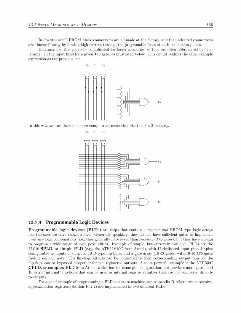
13.7 State Machines with Memory 335
In (“write-once”) PROM, these connections are all made at the factory, and the undesired connectionsare “burned” away by flowing high current through the programable fuses at each connection points.
Diagrams like this get to be complicated for larger memories, so they are often abbreviated by “col-lapsing” all the input lines for a given AND gate, as illustrated below. This circuit realizes the same exampleexpression as the previous one.
A0 A1 A2
O0
In this way, we can draw out more complicated memories, like this 3× 3 memory.
A0 A1 A2
O0
O1
O2
13.7.4 Programmable Logic Devices
Programmable logic devices (PLDs) are chips that contain a register and PROM-type logic arrayslike the ones we have shown above. Generally speaking, they do not have sufficient gates to implementarbitrary logic combinations (i.e., they generally have fewer than necessary AND gates), but they have enoughto program a wide range of logic possibilities. Example of simple, but currently available, PLDs are the22V10 SPLD, or simple PLD (e.g., the ATF22V10C from Atmel), with 12 dedicated input pins, 10 pinsconfigurable as inputs or outputs, 10 D-type flip-flops, and a gate array (10 OR gates, with 10-16 AND gatesfeeding each OR gate. The flip-flop outputs can be connected to their corresponding output pins, or theflip-flops can be bypassed altogether for non-registered outputs. A more powerful example is the ATF750CCPLD, or complex PLD from Atmel, which has the same pin configuration, but provides more gates, and10 extra “internal” flip-flops that can be used as internal register variables that are not connected directlyto outputs.
For a good example of programming a PLD as a state machine, see Appendix B, where two successive-approximation registers (Section 16.2.2) are implemented in two different PLDs.

336 Chapter 13. Flip Flops
13.8 Circuit Practice
13.8.1 Basic Flip-Flops
For circuit practice, go through these three flip-flops.(a) First, label the inputs and remaining output. This is the first one we did, but do this without
peeking! Think through the whole truth table.
Q
(b) Work out the equivalence of the (a) circuit to this one (i.e., label the inputs and outputs). Trynot to use a truth table to do this, use a logic theorem to connect these.
(c) Work out the equivalence of the (b) circuit to this one (i.e., label the inputs and outputs). Try notto use a truth table to do this, use a logic theorem to connect these.
Solution.(a) The labeled version is:
R
S
Q
Q
(b) This is basically the same circuit, but with all inputs and outputs of gates negated. Thus, the flip-flopinputs and outputs are similarly negated. The labeled version is:
Q
Q
S
R
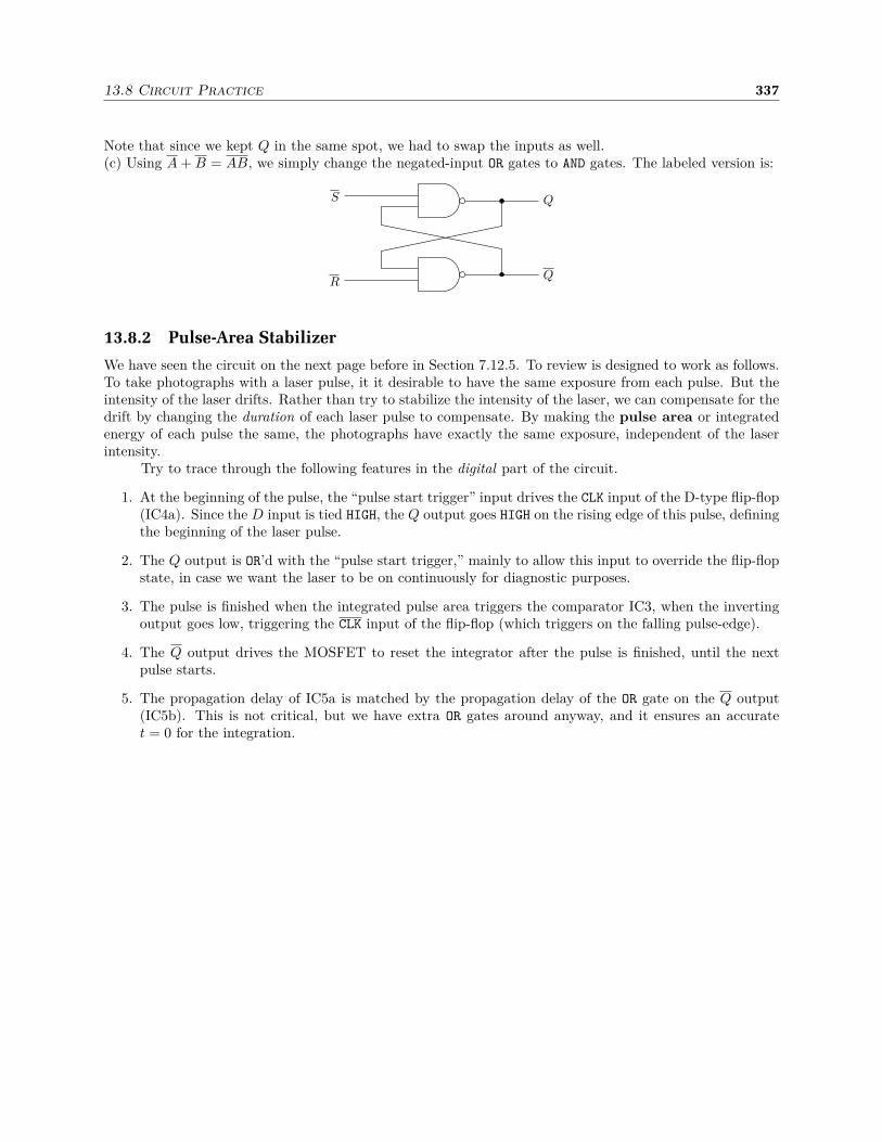
13.8 Circuit Practice 337
Note that since we kept Q in the same spot, we had to swap the inputs as well.(c) Using A + B = AB, we simply change the negated-input OR gates to AND gates. The labeled version is:
Q
Q
S
R
13.8.2 Pulse-Area Stabilizer
We have seen the circuit on the next page before in Section 7.12.5. To review is designed to work as follows.To take photographs with a laser pulse, it it desirable to have the same exposure from each pulse. But theintensity of the laser drifts. Rather than try to stabilize the intensity of the laser, we can compensate for thedrift by changing the duration of each laser pulse to compensate. By making the pulse area or integratedenergy of each pulse the same, the photographs have exactly the same exposure, independent of the laserintensity.
Try to trace through the following features in the digital part of the circuit.
1. At the beginning of the pulse, the “pulse start trigger” input drives the CLK input of the D-type flip-flop(IC4a). Since the D input is tied HIGH, the Q output goes HIGH on the rising edge of this pulse, definingthe beginning of the laser pulse.
2. The Q output is OR’d with the “pulse start trigger,” mainly to allow this input to override the flip-flopstate, in case we want the laser to be on continuously for diagnostic purposes.
3. The pulse is finished when the integrated pulse area triggers the comparator IC3, when the invertingoutput goes low, triggering the CLK input of the flip-flop (which triggers on the falling pulse-edge).
4. The Q output drives the MOSFET to reset the integrator after the pulse is finished, until the nextpulse starts.
5. The propagation delay of IC5a is matched by the propagation delay of the OR gate on the Q output(IC5b). This is not critical, but we have extra OR gates around anyway, and it ensures an accuratet = 0 for the integration.

338 Chapter 13. Flip Flops
A A
B B
C C
D D
E E
F F
G G
H H
11
22
33
44
55
66
PU
LSE
AR
EA
ST
AB
ILIZ
ER
12/
15/
07
D
. A
. Ste
ck,
J. J
. T
ho
rn
IC5
bypass
IC4
bypass
dra
in t
ime 3
3ns
1V
, 3
0µs p
uls
e
giv
es 3
V s
ignal
Puls
e C
ontr
ol
Out
(TTL)
Puls
e Sta
rt
Tri
gg
er
(0-5
V)
Puls
e A
rea
Set
Poin
t
Inte
gra
tor
Monit
or
Out
Photo
dio
de
Monit
or
Out
/P
RE
CLK
D /C
LR
Q
/Q
4 3 2 1
5 6
IC4
a
74F74N
10
k
R1
3
4
J3
BN
C
1000p
C1
3
4
J1
BN
C10
k
R2
3
4
J2
BN
C 10
k
R3
1µ
C2
+5V
3
4
J4
BN
C
3
4
J5
BN
C
Q1
33
R4
1k
R5
1M
R6
+5V
1 23
IC5
a
74
LS3
2
+ -1 2
3 4
LM
39
9
IC6
5k
R7 -1
2V
S1
22
3
PD
1
10
R8
10
R9
10
R1
0
10
R1
1
-12
V
-12
V
+12V
+12V
- +
2 3
4
1
5
7
6O
PA
60
2
IC1
0.1
µ
C5
0.1
µ
C6
0.1
µ
C7
0.1
µ
C8
-+ 4
2 3
1
5
6
78
IC3
TL3
01
6
- +
2 3
4
1
5
7
6O
PA
60
2IC
2
0.1
µ
C4
4 56
IC5
b
74
LS3
2
1µ
C3
12
3IC
7LM
78
12
2
1
3
IC8
LM
79
12
1
2
3IC
9LM
78
05
+1
5GN
D-1
5
J6
+12V
-12
V
+12V
10
µ
C9
10
µ
C1
3
10
µ
C1
0
+5V
0.1
µC1
1
0.1
µC1
2
0.1
µC1
40
.1µ
C1
50
.1µ
C1
6
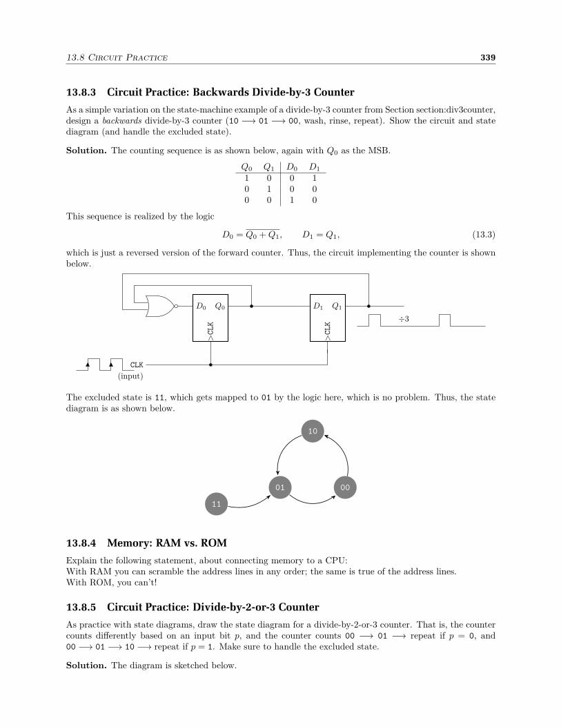
13.8 Circuit Practice 339
13.8.3 Circuit Practice: Backwards Divide-by-3 Counter
As a simple variation on the state-machine example of a divide-by-3 counter from Section section:div3counter,design a backwards divide-by-3 counter (10 −→ 01 −→ 00, wash, rinse, repeat). Show the circuit and statediagram (and handle the excluded state).
Solution. The counting sequence is as shown below, again with Q0 as the MSB.
Q0 Q1 D0 D1
1 0 0 10 1 0 00 0 1 0
This sequence is realized by the logic
D0 = Q0 + Q1, D1 = Q1, (13.3)
which is just a reversed version of the forward counter. Thus, the circuit implementing the counter is shownbelow.
D0
>CLK
Q0
CLK
(input)
D1
>CLK
Q1
÷3
The excluded state is 11, which gets mapped to 01 by the logic here, which is no problem. Thus, the statediagram is as shown below.
10
0001
11
13.8.4 Memory: RAM vs. ROM
Explain the following statement, about connecting memory to a CPU:With RAM you can scramble the address lines in any order; the same is true of the address lines.With ROM, you can’t!
13.8.5 Circuit Practice: Divide-by-2-or-3 Counter
As practice with state diagrams, draw the state diagram for a divide-by-2-or-3 counter. That is, the countercounts differently based on an input bit p, and the counter counts 00 −→ 01 −→ repeat if p = 0, and00 −→ 01 −→ 10 −→ repeat if p = 1. Make sure to handle the excluded state.
Solution. The diagram is sketched below.

340 Chapter 13. Flip Flops
00
0110
11 p = X
p = 1
p = 0
p = X
p = X
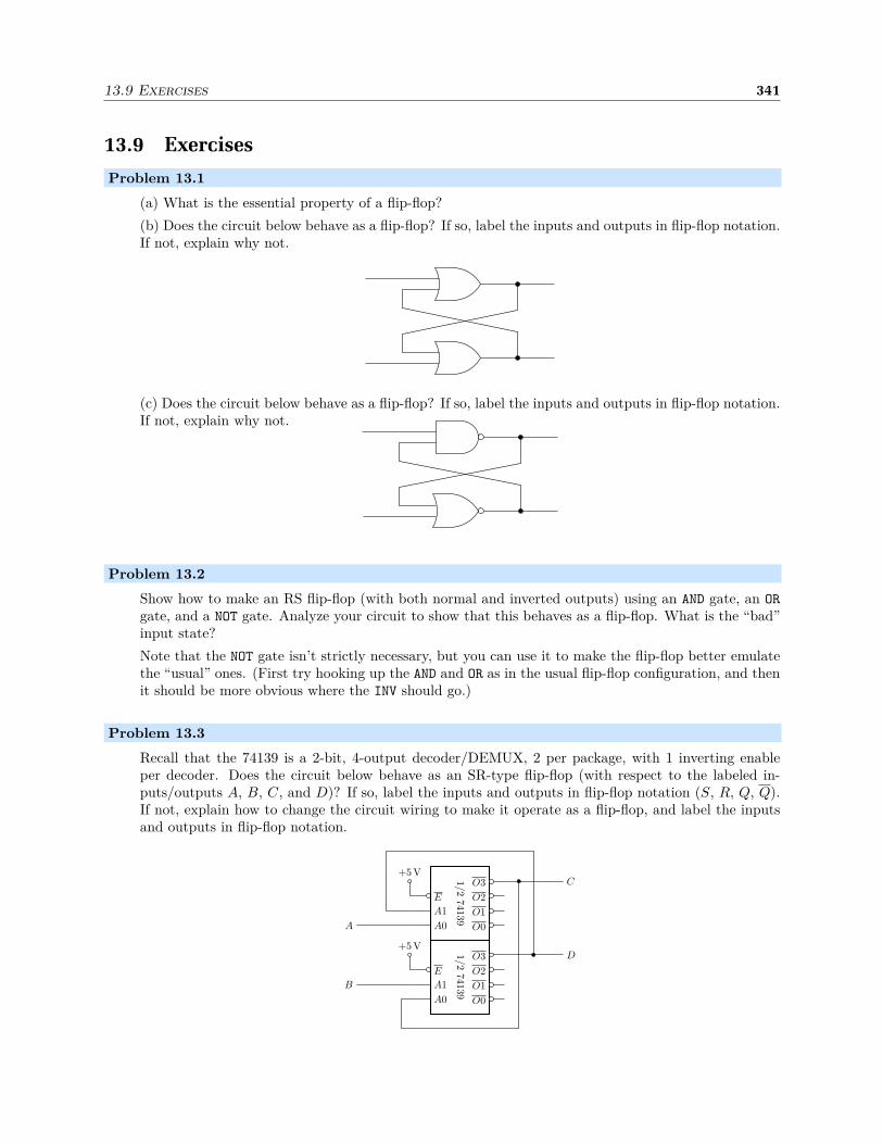
13.9 Exercises 341
13.9 Exercises
Problem 13.1
(a) What is the essential property of a flip-flop?
(b) Does the circuit below behave as a flip-flop? If so, label the inputs and outputs in flip-flop notation.If not, explain why not.
(c) Does the circuit below behave as a flip-flop? If so, label the inputs and outputs in flip-flop notation.If not, explain why not.
Problem 13.2
Show how to make an RS flip-flop (with both normal and inverted outputs) using an AND gate, an OR
gate, and a NOT gate. Analyze your circuit to show that this behaves as a flip-flop. What is the “bad”input state?
Note that the NOT gate isn’t strictly necessary, but you can use it to make the flip-flop better emulatethe “usual” ones. (First try hooking up the AND and OR as in the usual flip-flop configuration, and thenit should be more obvious where the INV should go.)
Problem 13.3
Recall that the 74139 is a 2-bit, 4-output decoder/DEMUX, 2 per package, with 1 inverting enableper decoder. Does the circuit below behave as an SR-type flip-flop (with respect to the labeled in-puts/outputs A, B, C, and D)? If so, label the inputs and outputs in flip-flop notation (S, R, Q, Q).If not, explain how to change the circuit wiring to make it operate as a flip-flop, and label the inputsand outputs in flip-flop notation.
1/274139
1/274139
O3
O2
O1
O0
E
A1
A0
O3
O2
O1
O0
E
A1
A0
A
B
+5 V
+5 V
C
D
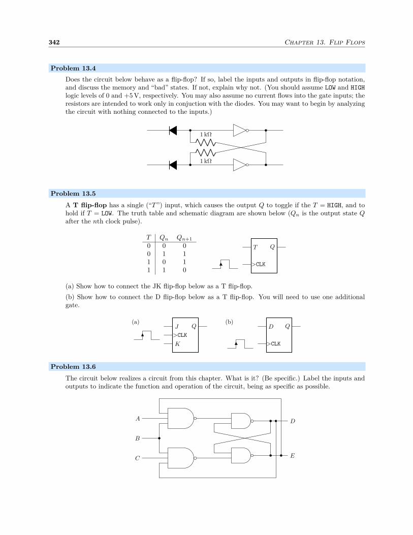
342 Chapter 13. Flip Flops
Problem 13.4
Does the circuit below behave as a flip-flop? If so, label the inputs and outputs in flip-flop notation,and discuss the memory and “bad” states. If not, explain why not. (You should assume LOW and HIGH
logic levels of 0 and +5 V, respectively. You may also assume no current flows into the gate inputs; theresistors are intended to work only in conjuction with the diodes. You may want to begin by analyzingthe circuit with nothing connected to the inputs.)
1 kΩ
1 kΩ
Problem 13.5
A T flip-flop has a single (“T”) input, which causes the output Q to toggle if the T = HIGH, and tohold if T = LOW. The truth table and schematic diagram are shown below (Qn is the output state Qafter the nth clock pulse).
T Qn Qn+1
0 0 00 1 11 0 11 1 0
T
>CLK
Q
(a) Show how to connect the JK flip-flop below as a T flip-flop.
(b) Show how to connect the D flip-flop below as a T flip-flop. You will need to use one additionalgate.
J
K
>CLK
Q(a)
D
>CLK
Q(b)
Problem 13.6
The circuit below realizes a circuit from this chapter. What is it? (Be specific.) Label the inputs andoutputs to indicate the function and operation of the circuit, being as specific as possible.
D
E
B
A
C
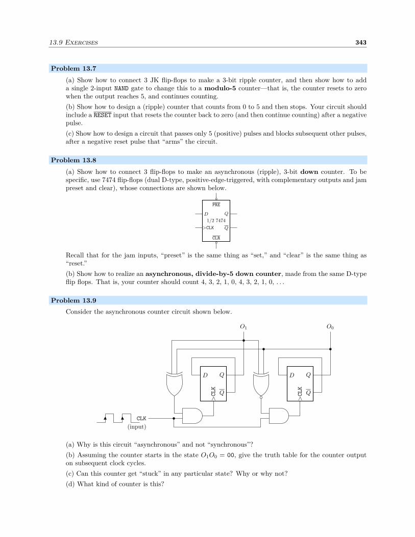
13.9 Exercises 343
Problem 13.7
(a) Show how to connect 3 JK flip-flops to make a 3-bit ripple counter, and then show how to adda single 2-input NAND gate to change this to a modulo-5 counter—that is, the counter resets to zerowhen the output reaches 5, and continues counting.
(b) Show how to design a (ripple) counter that counts from 0 to 5 and then stops. Your circuit shouldinclude a RESET input that resets the counter back to zero (and then continue counting) after a negativepulse.
(c) Show how to design a circuit that passes only 5 (positive) pulses and blocks subsequent other pulses,after a negative reset pulse that “arms” the circuit.
Problem 13.8
(a) Show how to connect 3 flip-flops to make an asynchronous (ripple), 3-bit down counter. To bespecific, use 7474 flip-flops (dual D-type, positive-edge-triggered, with complementary outputs and jampreset and clear), whose connections are shown below.
1/2 7474
D
>CLK
Q
Q
PRE
CLR
Recall that for the jam inputs, “preset” is the same thing as “set,” and “clear” is the same thing as“reset.”
(b) Show how to realize an asynchronous, divide-by-5 down counter, made from the same D-typeflip flops. That is, your counter should count 4, 3, 2, 1, 0, 4, 3, 2, 1, 0, . . .
Problem 13.9
Consider the asynchronous counter circuit shown below.
D
>CLK
Q
Q
CLK
(input)
O1
D
>CLK
Q
Q
O0
(a) Why is this circuit “asynchronous” and not “synchronous”?
(b) Assuming the counter starts in the state O1O0 = 00, give the truth table for the counter outputon subsequent clock cycles.
(c) Can this counter get “stuck” in any particular state? Why or why not?
(d) What kind of counter is this?

344 Chapter 13. Flip Flops
Problem 13.10
Describe precisely and completely but concisely the operation of the circuit below, including all inputsI0–I3 and outputs O0–O1.
D
CLK
Q
Q
S
R
D
CLK
Q
Q
S
R
O0
O1
I2
I3
I0
I1
CLK
Problem 13.11
The 7490 is a decade counter, with clock inputs that trigger on falling edges. Below are two ways toconnect the 7490 as a divide-by-10 counter. However, they are not equivalent. What, specifically, isthe difference in the output waveforms? (Be quantitative.) Also, remember QB is the least significantbit of the divide-by-5 subcounter.
/5
/2
clock B
clock A= input
1
14 QA
QBQCQD = output
12
98
11RESET
+5 V 5
7 10 2 3
7490
(a)
/5
/2
clock B= input
clock A
1
14 QA = output
QBQCQD
12
98
11RESET
+5 V 5
7 10 2 3
7490
(b)
Problem 13.12
Design a synchronous 2-bit UP/DOWN counter: It has a clock input, and a control input (U/D); theoutputs are the two flip-flop outputs Q1 and Q2. If U/D is HIGH, it goes through a normal binarycounting sequence; if LOW, it counts backward—Q2Q1 = 00, 11, 10, 01, 00, . . .4
Problem 13.13
Design a synchronous, 3-bit Fibonacci counter (i.e., count through the Fibonacci numbers 0, 1, 2, 3,5, and then repeat). Use three flip-flops (of the 7474 type, as shown above) and whatever gates you
4Paul Horowitz and Winfield Hill, The Art of Electronics, 2nd ed. (Cambridge, 1989), Exercise 8.25 (ISBN: 0521370957).
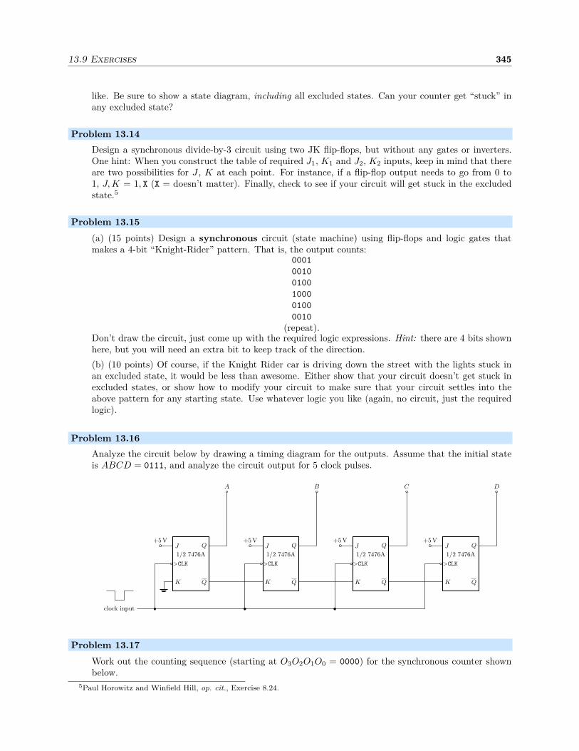
13.9 Exercises 345
like. Be sure to show a state diagram, including all excluded states. Can your counter get “stuck” inany excluded state?
Problem 13.14
Design a synchronous divide-by-3 circuit using two JK flip-flops, but without any gates or inverters.One hint: When you construct the table of required J1, K1 and J2, K2 inputs, keep in mind that thereare two possibilities for J , K at each point. For instance, if a flip-flop output needs to go from 0 to1, J, K = 1, X (X = doesn’t matter). Finally, check to see if your circuit will get stuck in the excludedstate.5
Problem 13.15
(a) (15 points) Design a synchronous circuit (state machine) using flip-flops and logic gates thatmakes a 4-bit “Knight-Rider” pattern. That is, the output counts:
0001
0010
0100
1000
0100
0010
(repeat).Don’t draw the circuit, just come up with the required logic expressions. Hint: there are 4 bits shownhere, but you will need an extra bit to keep track of the direction.
(b) (10 points) Of course, if the Knight Rider car is driving down the street with the lights stuck inan excluded state, it would be less than awesome. Either show that your circuit doesn’t get stuck inexcluded states, or show how to modify your circuit to make sure that your circuit settles into theabove pattern for any starting state. Use whatever logic you like (again, no circuit, just the requiredlogic).
Problem 13.16
Analyze the circuit below by drawing a timing diagram for the outputs. Assume that the initial stateis ABCD = 0111, and analyze the circuit output for 5 clock pulses.
1/2 7476A
J
>CLK
K
Q
Q
1/2 7476A
J
>CLK
K
Q
Q
1/2 7476A
J
>CLK
K
Q
Q
1/2 7476A
J
>CLK
K
Q
Q
clock input
A B C D
+5 V +5 V +5 V +5 V
Problem 13.17
Work out the counting sequence (starting at O3O2O1O0 = 0000) for the synchronous counter shownbelow.
5Paul Horowitz and Winfield Hill, op. cit., Exercise 8.24.

346 Chapter 13. Flip Flops
74112
J
K
Q
>CLK
74112
J
K
Q
>CLK
74112
J
K
Q
>CLK
74112
J
K
Q
>CLK
CLK input
O0 O1 O2 O3
+5 V
Problem 13.18
Design a synchronous, divide-by-16 counter. Just work out Boolean expressions for the required logicusing the design procedure for the state machine; no need to draw a circuit schematic. (Write youroutput bits as Q3Q2Q1Q0 from MSB to LSB.)
Problem 13.19
Consider the ripple-counter circuit shown below, with control inputs CJ and CK .
74112
J
>CLK
K
Q
74112
J
>CLK
K
Q
74112
J
>CLK
K
Q
CLK input
O0 O1 O2
CJ
CK
What control-input combination CJCK is necessary for the circuit to count, and what kind of counteris it? Describe the operation of this circuit for all other control-input combinations CJCK .
Problem 13.20
(a) Design a synchronous 4-bit, binary counter, using JK flip-flops (use the same 74112’s as shownin Problem 13.19), by considering the following: Think about how binary counting works, and inparticular, what is the condition for a particular bit to toggle its state during the counting sequence?How do you switch between toggling or holding in a JK flip-flop?
(b) Design a synchronous 4-bit, binary counter, as in part (a), but this time using D flip-flops. Usethe same hint from part (a). What kind of gate acts as a conditional inverter?
Problem 13.21
(a) Design an asynchronous/ripple BCD counter (i.e., counts up in binary from 0–9 and then resets).Use JK flip-flops as in Problem 1, but include (and use) jam-reset inputs R.
(b) To drive a two-digit decimal display that counts from 00–99 (then resets), you would need toprovide an output to drive the counter for the next digit. Indicate how you would do this in yourcircuit, and how it connects to the counter for the next digit.
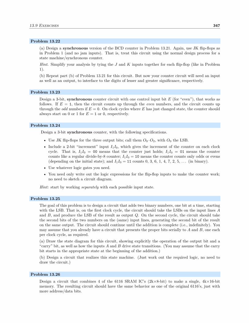
13.9 Exercises 347
Problem 13.22
(a) Design a synchronous version of the BCD counter in Problem 13.21. Again, use JK flip-flops asin Problem 1 (and no jam inputs). That is, treat this circuit using the normal design process for astate machine/synchronous counter.
Hint. Simplify your analysis by tying the J and K inputs together for each flip-flop (like in Problem1).
(b) Repeat part (b) of Problem 13.21 for this circuit. But now your counter circuit will need an inputas well as an output, to interface to the digits of lesser and greater significance, respectively.
Problem 13.23
Design a 3-bit, synchronous counter circuit with one control input bit E (for “even”), that works asfollows. If E = 1, then the circuit counts up through the even numbers, and the circuit counts upthrough the odd numbers if E = 0. On clock cycles where E has just changed state, the counter shouldalways start on 0 or 1 for E = 1 or 0, respectively.
Problem 13.24
Design a 3-bit synchronous counter, with the following specifications.
• Use JK flip-flops for the three output bits; call them O0–O2, with O0 the LSB.
• Include a 2-bit “increment” input I1I0, which gives the increment of the counter on each clockcycle. That is, I1I0 = 00 means that the counter just holds; I1I0 = 01 means the countercounts like a regular divide-by-8 counter; I1I0 = 10 means the counter counts only odds or evens(depending on the initial state); and I1I0 = 11 counts 0, 3, 6, 1, 4, 7, 2, 5, . . . (in binary).
• Use whatever logic gates you need.
• You need only write out the logic expressions for the flip-flop inputs to make the counter work;no need to sketch a circuit diagram.
Hint: start by working separately with each possible input state.
Problem 13.25
The goal of this problem is to design a circuit that adds two binary numbers, one bit at a time, startingwith the LSB. That is, on the first clock cycle, the circuit should take the LSBs on the input lines Aand B, and produce the LSB of the result as output Q. On the second cycle, the circuit should takethe second bits of the two numbers on the (same) input lines, generating the second bit of the resulton the same output. The circuit should continue until the addition is complete (i.e., indefinitely). Youmay assume that you already have a circuit that presents the proper bits serially to A and B, one eachper clock cycle, as required.
(a) Draw the state diagram for this circuit, showing explicitly the operation of the output bit and a“carry” bit, as well as how the inputs A and B drive state transitions. (You may assume that the carrybit starts in the appropriate state at the beginning of the addition.)
(b) Design a circuit that realizes this state machine. (Just work out the required logic, no need todraw the circuit.)
Problem 13.26
Design a circuit that combines 4 of the 6116 SRAM IC’s (2k×8-bit) to make a single, 4k×16-bitmemory. The resulting circuit should have the same behavior as one of the original 6116’s, just withmore address/data bits.

348 Chapter 13. Flip Flops
Problem 13.27
A 3-bit register and an 8× 3 ROM are connected as shown below.
D0
D1
D2
>CLK
Q0
Q1
Q2
ROM
O2
O1
O0
A2
A1
A0
A2A
1A
0=
Q2Q
1Q
0
D2 D
1 D0
=O
2 O1 O
0
Register
The ROM is programmed as follows:
A2 A1 A0 O2 O1 O0
0 0 0 1 0 0
0 0 1 0 1 0
0 1 0 0 0 0
0 1 1 0 1 1
1 0 0 1 1 0
1 0 1 0 0 0
1 1 0 1 1 1
1 1 1 0 0 1
Assume that the initial state of the register is Q2Q1Q0 = 010.
(a) Give the state of the register outputs Q2Q1Q0 after each of the next three clock pulses.
(b) Even after arbitrarily many clock pulses, (at least) one possible value of Q2Q1Q0 will never occur.Which?
Problem 13.28
Show how to connect a T flip-flop as a D flip-flop (shown below). (The operation of the T flip-flop isdefined in Problem 13.5.) Use whatever extra logic gates you need (simple two-input gates only).
D
>CLK
Q
Hint: if you don’t see how to get started, treat the problem as a state machine with current state Qn
and external input D.
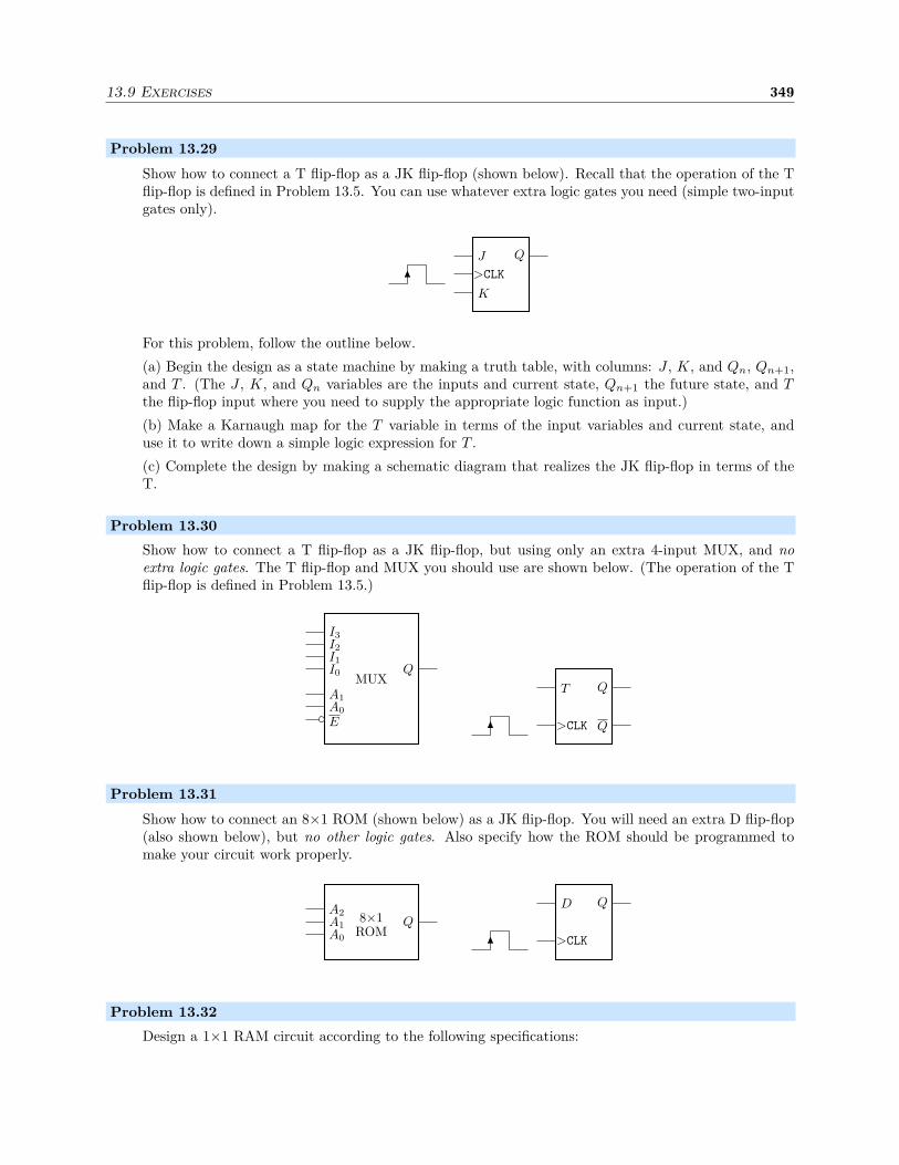
13.9 Exercises 349
Problem 13.29
Show how to connect a T flip-flop as a JK flip-flop (shown below). Recall that the operation of the Tflip-flop is defined in Problem 13.5. You can use whatever extra logic gates you need (simple two-inputgates only).
J
K
>CLK
Q
For this problem, follow the outline below.
(a) Begin the design as a state machine by making a truth table, with columns: J , K, and Qn, Qn+1,and T . (The J , K, and Qn variables are the inputs and current state, Qn+1 the future state, and Tthe flip-flop input where you need to supply the appropriate logic function as input.)
(b) Make a Karnaugh map for the T variable in terms of the input variables and current state, anduse it to write down a simple logic expression for T .
(c) Complete the design by making a schematic diagram that realizes the JK flip-flop in terms of theT.
Problem 13.30
Show how to connect a T flip-flop as a JK flip-flop, but using only an extra 4-input MUX, and no
extra logic gates. The T flip-flop and MUX you should use are shown below. (The operation of the Tflip-flop is defined in Problem 13.5.)
MUX
EA0
A1
I0
I1
I2
I3
Q
T
>CLK
Q
Q
Problem 13.31
Show how to connect an 8×1 ROM (shown below) as a JK flip-flop. You will need an extra D flip-flop(also shown below), but no other logic gates. Also specify how the ROM should be programmed tomake your circuit work properly.
ROM8×1
A0
A1
A2Q
D
>CLK
Q
Problem 13.32
Design a 1×1 RAM circuit according to the following specifications:
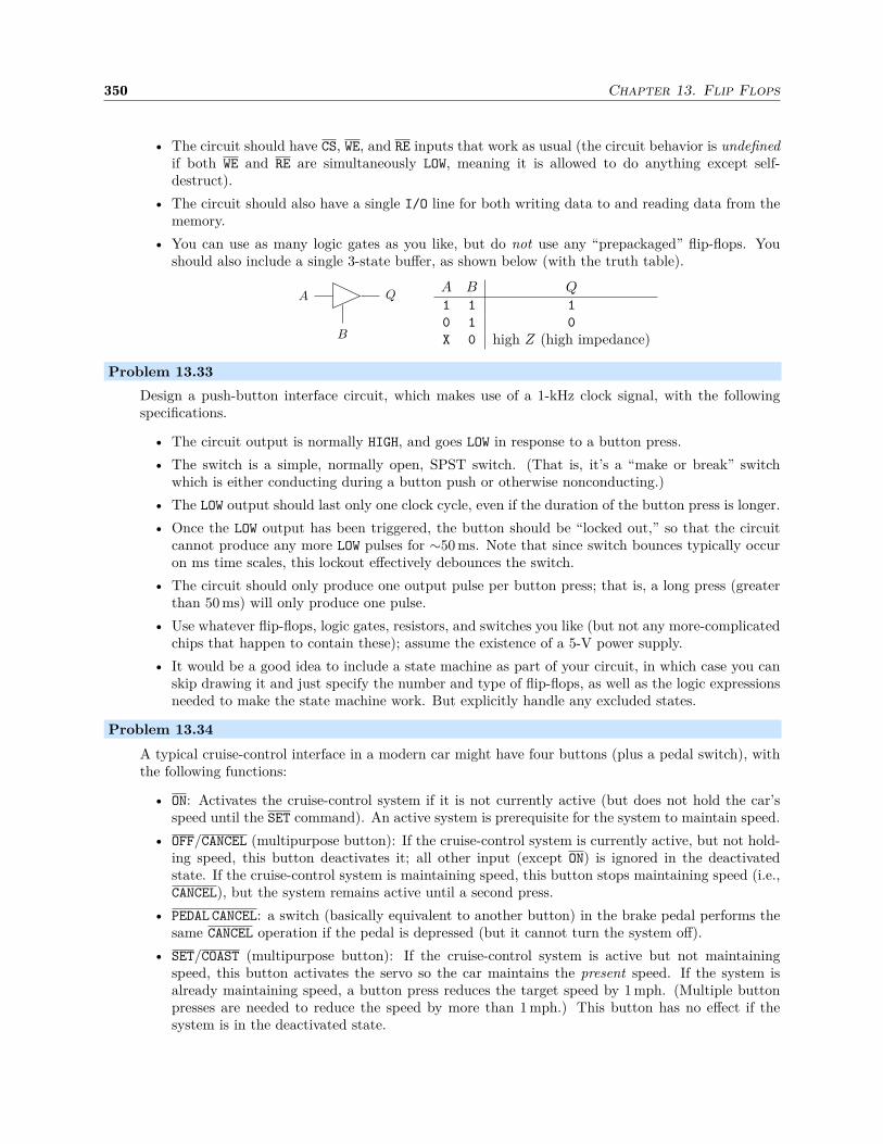
350 Chapter 13. Flip Flops
• The circuit should have CS, WE, and RE inputs that work as usual (the circuit behavior is undefined
if both WE and RE are simultaneously LOW, meaning it is allowed to do anything except self-destruct).
• The circuit should also have a single I/O line for both writing data to and reading data from thememory.
• You can use as many logic gates as you like, but do not use any “prepackaged” flip-flops. Youshould also include a single 3-state buffer, as shown below (with the truth table).
QA
B
A B Q1 1 1
0 1 0
X 0 high Z (high impedance)
Problem 13.33
Design a push-button interface circuit, which makes use of a 1-kHz clock signal, with the followingspecifications.
• The circuit output is normally HIGH, and goes LOW in response to a button press.
• The switch is a simple, normally open, SPST switch. (That is, it’s a “make or break” switchwhich is either conducting during a button push or otherwise nonconducting.)
• The LOW output should last only one clock cycle, even if the duration of the button press is longer.
• Once the LOW output has been triggered, the button should be “locked out,” so that the circuitcannot produce any more LOW pulses for ∼50 ms. Note that since switch bounces typically occuron ms time scales, this lockout effectively debounces the switch.
• The circuit should only produce one output pulse per button press; that is, a long press (greaterthan 50 ms) will only produce one pulse.
• Use whatever flip-flops, logic gates, resistors, and switches you like (but not any more-complicatedchips that happen to contain these); assume the existence of a 5-V power supply.
• It would be a good idea to include a state machine as part of your circuit, in which case you canskip drawing it and just specify the number and type of flip-flops, as well as the logic expressionsneeded to make the state machine work. But explicitly handle any excluded states.
Problem 13.34
A typical cruise-control interface in a modern car might have four buttons (plus a pedal switch), withthe following functions:
• ON: Activates the cruise-control system if it is not currently active (but does not hold the car’sspeed until the SET command). An active system is prerequisite for the system to maintain speed.
• OFF/CANCEL (multipurpose button): If the cruise-control system is currently active, but not hold-ing speed, this button deactivates it; all other input (except ON) is ignored in the deactivatedstate. If the cruise-control system is maintaining speed, this button stops maintaining speed (i.e.,CANCEL), but the system remains active until a second press.
• PEDAL CANCEL: a switch (basically equivalent to another button) in the brake pedal performs thesame CANCEL operation if the pedal is depressed (but it cannot turn the system off).
• SET/COAST (multipurpose button): If the cruise-control system is active but not maintainingspeed, this button activates the servo so the car maintains the present speed. If the system isalready maintaining speed, a button press reduces the target speed by 1 mph. (Multiple buttonpresses are needed to reduce the speed by more than 1 mph.) This button has no effect if thesystem is in the deactivated state.

13.9 Exercises 351
• RESUME/ACCEL (multipurpose button): If the cruise-control system is active but not maintainingspeed, this button activates the servo so the car maintains the previously held target speed (as-suming some speed was in fact previously held; otherwise the button should do nothing). If thesystem is already maintaining speed, a button press increases the target speed by 1 mph. Multiplebutton presses are needed to increase the speed by more than 1 mph. This button has no effect ifthe system is in the deactivated state.
The bars over the button names emphasize that the button output is normally HIGH, and active LOW
(momentarily, during a button press).
Your task as a newly employed engineer of the Schmoyota Motor Corporation is to design the interfacelogic for the cruise-control system for next year’s Schmoyota Schmius. That is, design a statemachine and its logic implementation to take the five buttons as input, and to provide outputsto an existing cruise-control servo module (which does all the work of sensing and holding the currentspeed; this means you don’t have to track or deal directly with the speed in your circuit). The fiveinputs to the servo module (all to be connected to your circuit, but to reiterate, all of the below servofunctionality has been implemented already by another engineer) are as follows:
• ACTIVE: When LOW, this input activates a light on the instrument cluster to show the driver thatthe cruise-control system is active and ready to start maintaining speed.
• MAINTAIN: This input activates the speed servo, causing the car to hold constant speed. Activatingthis input also causes the target speed (in mph) to be displayed on the instrument cluster.
• SET/RESUME: Right after the falling edge of MAINTAIN, when the car begins to hold speed, thesystem needs to know if it should hold the current speed or the last held speed. If HIGH, this inputtells the servo to hold the current speed, while if LOW, the servo should set the target speed to thepreviously held target. Do not tell the servo to hold a previous target unless the system has infact held some previous target speed; otherwise the system will attempt to hold some undefined(random) speed, which may not be very nice for the driver!
• SPEEDUP: Pulse this input LOW to increment the target speed by 1 mph (pulse only while MAINTAIN =LOW).
• SLOWDOWN: Pulse this input LOW to decrement the target speed by 1 mph (pulse only whileMAINTAIN = LOW).
For your state machine, you should use 4 D-type flip-flops: three will drive the servo inputs ACTIVE,MAINTAIN, and SET/RESUME, plus you should use another flip-flop with output ALREADY, which is LOW
if (and only if) a speed has already been held since the system was activated. You can take SPEEDUP
and SLOWDOWN to be extra outputs of your state machine.
Assume that a clock source has already been provided (at some reasonably high frequency so theinterface seems to respond instantaneously, as far as the driver is concerned). Also assume that thebuttons are connected via the circuit of Problem 13.33, so that a button press coincides with exactlyone clock cycle, and bounce is not an issue.
(a) Write down a truth table defining the operation of your state machine according to the abovespecifications. Your table should include the current and future states of the four flip-flops, plus thefive button inputs. Make use of the X = “either” notation to avoid writing out all 29 individualtruth-table entries!
(b) Derive logic expressions for the inputs of the four flip-flops, as well as the SPEEDUP and SLOWDOWN
inputs to the servo. (No need to draw the circuit.)
Problem 13.35
In the circuit of Problem 13.34, which of the buttons would produce undesired behavior if the buttonwere not debounced? Briefly explain.
(Note that you don’t need to solve that problem to solve this one.)

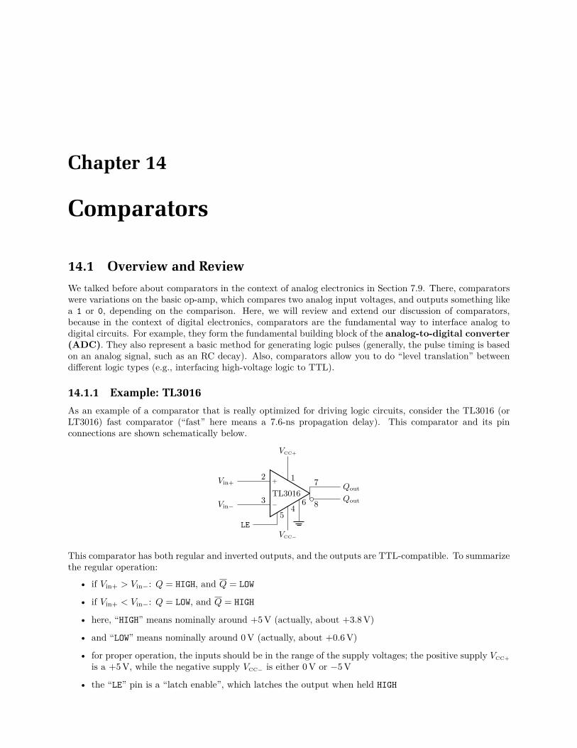
Chapter 14
Comparators
14.1 Overview and Review
We talked before about comparators in the context of analog electronics in Section 7.9. There, comparatorswere variations on the basic op-amp, which compares two analog input voltages, and outputs something likea 1 or 0, depending on the comparison. Here, we will review and extend our discussion of comparators,because in the context of digital electronics, comparators are the fundamental way to interface analog todigital circuits. For example, they form the fundamental building block of the analog-to-digital converter(ADC). They also represent a basic method for generating logic pulses (generally, the pulse timing is basedon an analog signal, such as an RC decay). Also, comparators allow you to do “level translation” betweendifferent logic types (e.g., interfacing high-voltage logic to TTL).
14.1.1 Example: TL3016
As an example of a comparator that is really optimized for driving logic circuits, consider the TL3016 (orLT3016) fast comparator (“fast” here means a 7.6-ns propagation delay). This comparator and its pinconnections are shown schematically below.
−
+
TL3016Qout
Qout
Vin+
Vin−
VCC+
VCC−
4
12
3
7
86
LE5
This comparator has both regular and inverted outputs, and the outputs are TTL-compatible. To summarizethe regular operation:
• if Vin+ > Vin−: Q = HIGH, and Q = LOW
• if Vin+ < Vin−: Q = LOW, and Q = HIGH
• here, “HIGH” means nominally around +5 V (actually, about +3.8 V)
• and “LOW” means nominally around 0 V (actually, about +0.6 V)
• for proper operation, the inputs should be in the range of the supply voltages; the positive supply VCC+
is a +5 V, while the negative supply VCC−is either 0 V or −5 V
• the “LE” pin is a “latch enable”, which latches the output when held HIGH
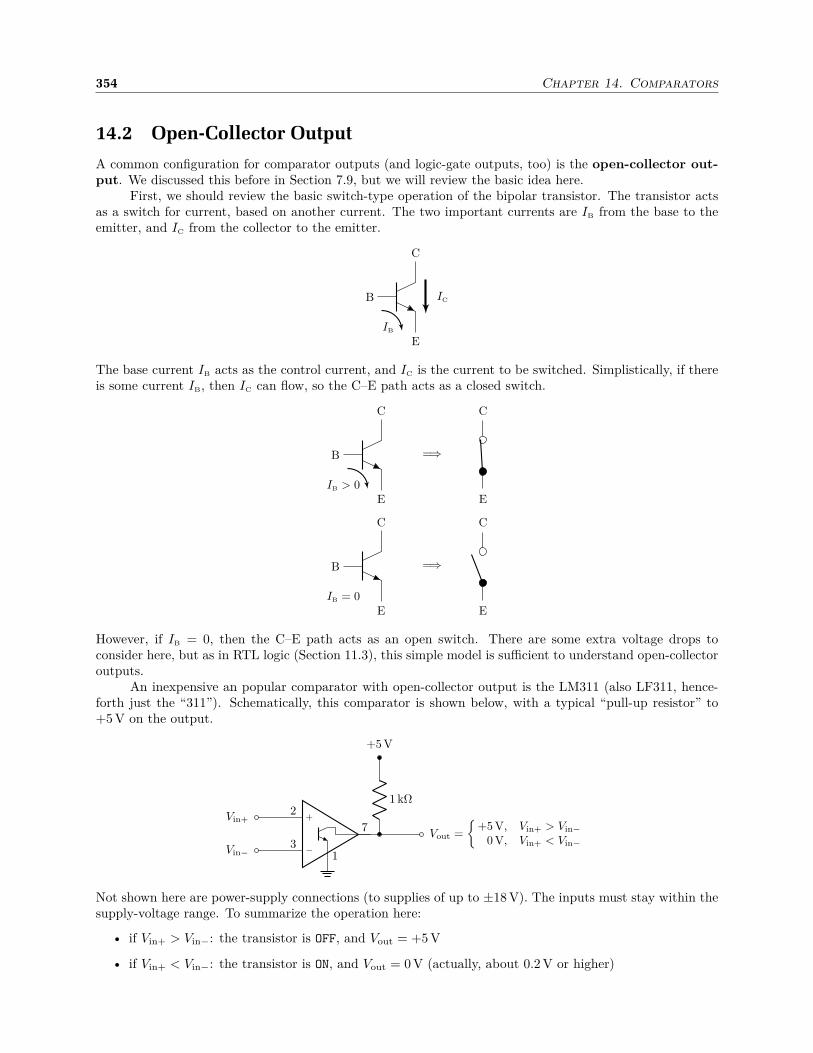
354 Chapter 14. Comparators
14.2 Open-Collector Output
A common configuration for comparator outputs (and logic-gate outputs, too) is the open-collector out-put. We discussed this before in Section 7.9, but we will review the basic idea here.
First, we should review the basic switch-type operation of the bipolar transistor. The transistor actsas a switch for current, based on another current. The two important currents are IB from the base to theemitter, and IC from the collector to the emitter.
B
C
E
IC
IB
The base current IB acts as the control current, and IC is the current to be switched. Simplistically, if thereis some current IB, then IC can flow, so the C–E path acts as a closed switch.
B
C
EIB > 0
=⇒
C
E
B
C
EIB = 0
=⇒
C
E
However, if IB = 0, then the C–E path acts as an open switch. There are some extra voltage drops toconsider here, but as in RTL logic (Section 11.3), this simple model is sufficient to understand open-collectoroutputs.
An inexpensive an popular comparator with open-collector output is the LM311 (also LF311, hence-forth just the “311”). Schematically, this comparator is shown below, with a typical “pull-up resistor” to+5 V on the output.
−
+
Vout =
+5 V, Vin+ > Vin−
0 V, Vin+ < Vin−
1 kΩ
+5 V
Vin+
Vin− 1
2
3
7
Not shown here are power-supply connections (to supplies of up to ±18 V). The inputs must stay within thesupply-voltage range. To summarize the operation here:
• if Vin+ > Vin−: the transistor is OFF, and Vout = +5 V
• if Vin+ < Vin−: the transistor is ON, and Vout = 0 V (actually, about 0.2 V or higher)

14.3 Schmitt Trigger 355
The point of the open-collector output is its flexibility: it’s not restricted to particular voltages like theoutputs of normal TTL gates. For example, the 311 can drive loads up to 40 V and 50 mA, so it can directlycontrol LEDs, lamps, relays, and so on. By contrast, a TTL-gate outputs would need a buffer transistor.
Another feature of the 311 is a TTL strobe input. A typical connection for this pin is shown below.
−
+
1 kΩ
+5 V
1 kΩ
TTL strobe in
(HIGH = disable, output is HIGH/ignore inputs)
6
If the strobe input is held HIGH, then the output is disabled: the output is HIGH (i.e., the output transistoropens), and the comparator ignores the inputs. This is useful for “gated” operation, if the comparator shouldonly trigger during some time interval or some condition determined by other logic.
14.3 Schmitt Trigger
We also discussed the Schmitt trigger in the context of analog circuits before in Section 7.9.1. We willreview the basic idea again here, since these are so important in digital applications that many logic deviceshave integrated Schmitt triggers.
The motivation for the Schmitt trigger comes from noisy inputs signals. Typically, these are slowlychanging analog signals, but even “digital” signals are fundamentally analog, and are thus similarly suscepti-ble to noise. As illustrated below, a noisy signal that is rising and falling can cause many spurious transitionswhile crossing the threshold.
V
t
threshold
V
t
Ideally, with a noise-free signal, the output (shown in the bottom plot) would have one up transition, thenlater a down transition, and then an up transition again, instead of the many clustered around the three“ideal” trigger times.

356 Chapter 14. Comparators
To analyze the fix for this, we will briefly review the voltage divider (see Section 1.3.3 and Problem 1.2).Given a series pair of resistors supplied by Vin, the output voltage at the tap point is given in terms of the“fractional resistance” at the tap point.
R1
Vin
R2
Vout =
(
R2
R1 + R2
)
Vin
If there are two voltages at either end of the resistor pair, the output voltage is a linear combination of thetwo voltages, given by the fractional resistances:
R1
Vin
R2
Vref
Vout =
(
R2
R1 + R2
)
Vin +
(
R1
R1 + R2
)
Vref
We can deduce the second result from the first by subtracting Vref from all voltages, and applying the first(grounded) result, to give
Vout − Vref =
(
R2
R1 + R2
)
(Vin − Vref). (14.1)
Rearranging gives the result in the figure. Note: you should memorize both of these voltage-divider formulas,and be able to quickly come up with resistor combinations that divide a voltage by 2, 3, etc.
Now consider the following circuit, which is a comparator with two added resistors. One resistor is inseries with the “trigger voltage” Vref , and another, large resistor ties the output to the noninverting input.
−
+
311 Vout
1 kΩ
+5 V
Vin
1 MΩ
10 kΩ
Vref

14.3 Schmitt Trigger 357
The extra resistors introduce hysteresis into the operation of the comparator as follows.
• if Vout = 0, V+ (the voltage at the noninverting input) is 0.99 Vref , using the first voltage-dividerformula.
• if Vout = +5 V, V+ = 0.99 Vref + 0.01 · 5 V, using the second voltage-divider formula.
Thus, the reference voltage changes by about 50 mV, depending on the output. Notice that
• if Vin = HIGH, the trigger point is lower
• if Vin = LOW, the trigger point is higher
So Vin “repels” the trigger point, which gives immunity to noise. The hysteresis of the Schmitt trigger issketched in the output-response plot below.
Vout
VinVref Vrefo+o50omV
+5oV
0oV
Note that the Schmitt trigger is bistable in the 50-mV-wide region near the nominal trigger voltage Vref .Thus, once the Schmitt trigger makes a transition, noise of less than around 50 mV will not cause anotherspurious transition.
Note that the configuration above is inverting, since Vin goes into the inverting input (i.e., large Vin
means the output is LOW). For a noninverting comparator, you can swap the Vin and Vref labels, but notethat the input is no longer well-isolated from the input, which may be a problem if the input source has highimpedance.
In digital circuits, many gates and logic devices are available with Schmitt-trigger inputs. An exampleis the 7414, a hex Schmitt-trigger inverter. This is shown schematically below.
Note the Schmitt-trigger symbol on the gate, which suggests the hysteresis curve. Schmitt-trigger-inputgates are good for signals without well-defined edges (like a sinusoidal input), or signals from an externalsource with a long cable run, which could be susceptible to noise pickup.
14.3.1 Example: Analog-to-Digital Clock-Signal Conversion
As an example application of a Schmitt trigger, consider the conversion of an analog clock signal to a digitalclock. An example of an analog clock source is a rubidium atomic clock, a relatively inexpensive (few $K)instrument that typically provides a 10-MHz sine wave, with a stability/accuracy of better than a part in1010. To drive digital circuits, however, this should be converted into an appropriate square wave withlogic-level inputs. The circuit below accomplishes this, using a Schmitt trigger to avoid spurious extra clockpulses due to noise on the clock signal.

358 Chapter 14. Comparators
−
+
TL3016 CLK out
50 kΩ50 kΩ50 kΩ
+5 V
thresholdoffset0.1 µF
50 Ω
CLKEXT
in
Note the ac-coupled input, a 50-Ω-terminated input (as appropriate for a 50-Ω cable connecting the clock tothis circuit), and the Schmitt trigger, with TTL-compatible output. The clock offset and threshold voltagesare adjustable to account for different input clock amplitudes, and to adjust the duty cycle of the resultingsquare wave (typically, these can both be set to 2.5 V).
14.4 Circuit Practice
For comparator practice, first note that you can light an LED with a power supply and a current-limitingresistor as follows.
10 kΩ
+15 V
Thus, an open-collector output can control the LED, since the output is either open or shorted to ground(corresponding to an OFF or ON LED, respectively).
Now design a “TTL out-of-range alarm,” given the following components and requirements:
• two 311’s
• any resistors you like
• an LED
• ±15-V power supplies (and ground)
• the circuit operates as follows: if Vin > +5 V or Vin < 0 V, the LED “alarm” lights; otherwise, the LEDis off
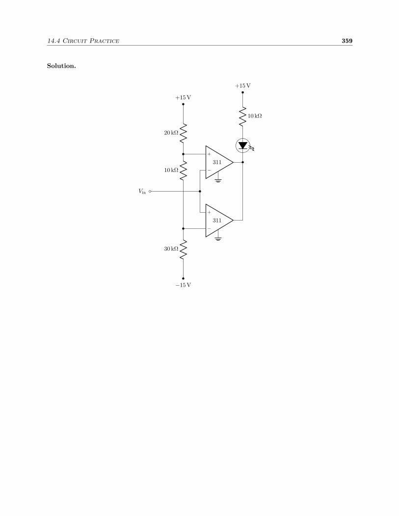
14.4 Circuit Practice 359
Solution.
−
+
311
−
+
311
10 kΩ
+15 V
Vin
20 kΩ
+15 V
10 kΩ
30 kΩ
−15 V

360 Chapter 14. Comparators
14.5 Exercises
Problem 14.1
(a) Show that the comparator circuit below acts as a flip-flop (“bistable multivibrator”). Label theset and reset inputs.
−
+
31110 kΩ
10 kΩ
Q
50 kΩ
3.3 kΩ
+5 V
100 kΩ
(b) Show how to add another (311) comparator to also produce the Q output. (Use whatever resistorsyou like.)
Problem 14.2
Briefly describe how a Schmitt trigger in an input of a logic gate can improve the performance of acircuit. Under what conditions on the input signal do you expect an improvement?
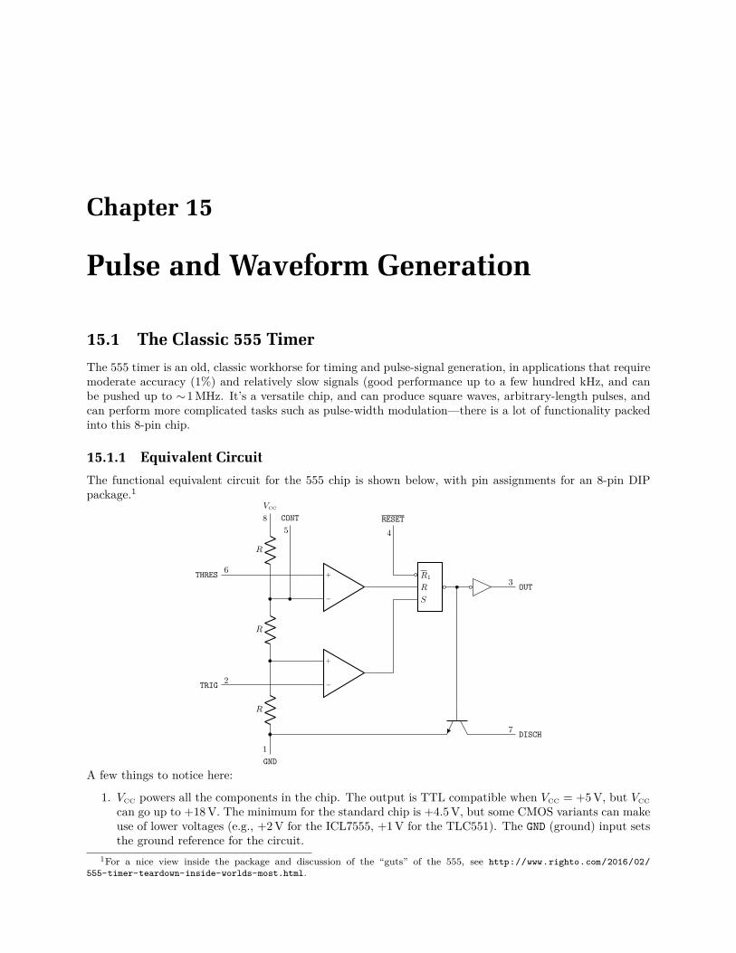
Chapter 15
Pulse and Waveform Generation
15.1 The Classic 555 Timer
The 555 timer is an old, classic workhorse for timing and pulse-signal generation, in applications that requiremoderate accuracy (1%) and relatively slow signals (good performance up to a few hundred kHz, and canbe pushed up to ∼1 MHz. It’s a versatile chip, and can produce square waves, arbitrary-length pulses, andcan perform more complicated tasks such as pulse-width modulation—there is a lot of functionality packedinto this 8-pin chip.
15.1.1 Equivalent Circuit
The functional equivalent circuit for the 555 chip is shown below, with pin assignments for an 8-pin DIPpackage.1
S
R
R1
−
+
−
+
RESET
4
OUT3
R
R
R
THRES6
TRIG2
VCC
8
GND
1
CONT
5
DISCH7
A few things to notice here:
1. VCC powers all the components in the chip. The output is TTL compatible when VCC = +5 V, but VCC
can go up to +18 V. The minimum for the standard chip is +4.5 V, but some CMOS variants can makeuse of lower voltages (e.g., +2 V for the ICL7555, +1 V for the TLC551). The GND (ground) input setsthe ground reference for the circuit.
1For a nice view inside the package and discussion of the “guts” of the 555, see http://www.righto.com/2016/02/
555-timer-teardown-inside-worlds-most.html.
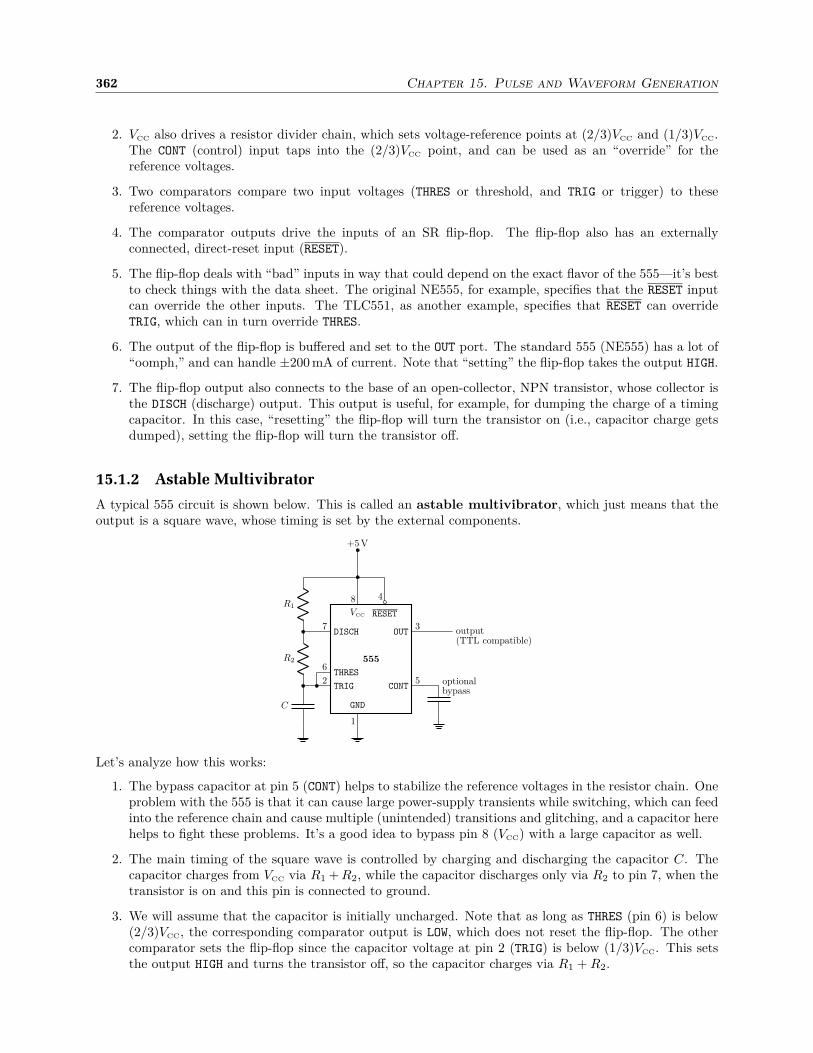
362 Chapter 15. Pulse and Waveform Generation
2. VCC also drives a resistor divider chain, which sets voltage-reference points at (2/3)VCC and (1/3)VCC.The CONT (control) input taps into the (2/3)VCC point, and can be used as an “override” for thereference voltages.
3. Two comparators compare two input voltages (THRES or threshold, and TRIG or trigger) to thesereference voltages.
4. The comparator outputs drive the inputs of an SR flip-flop. The flip-flop also has an externallyconnected, direct-reset input (RESET).
5. The flip-flop deals with “bad” inputs in way that could depend on the exact flavor of the 555—it’s bestto check things with the data sheet. The original NE555, for example, specifies that the RESET inputcan override the other inputs. The TLC551, as another example, specifies that RESET can overrideTRIG, which can in turn override THRES.
6. The output of the flip-flop is buffered and set to the OUT port. The standard 555 (NE555) has a lot of“oomph,” and can handle ±200 mA of current. Note that “setting” the flip-flop takes the output HIGH.
7. The flip-flop output also connects to the base of an open-collector, NPN transistor, whose collector isthe DISCH (discharge) output. This output is useful, for example, for dumping the charge of a timingcapacitor. In this case, “resetting” the flip-flop will turn the transistor on (i.e., capacitor charge getsdumped), setting the flip-flop will turn the transistor off.
15.1.2 Astable Multivibrator
A typical 555 circuit is shown below. This is called an astable multivibrator, which just means that theoutput is a square wave, whose timing is set by the external components.
555
THRES
TRIG
DISCH OUT
CONT
GND
1
R1
R2
C
7
6
2
3
5 optionalbypass
output(TTL compatible)
+5 V
8 4
VCC RESET
Let’s analyze how this works:
1. The bypass capacitor at pin 5 (CONT) helps to stabilize the reference voltages in the resistor chain. Oneproblem with the 555 is that it can cause large power-supply transients while switching, which can feedinto the reference chain and cause multiple (unintended) transitions and glitching, and a capacitor herehelps to fight these problems. It’s a good idea to bypass pin 8 (VCC) with a large capacitor as well.
2. The main timing of the square wave is controlled by charging and discharging the capacitor C. Thecapacitor charges from VCC via R1 + R2, while the capacitor discharges only via R2 to pin 7, when thetransistor is on and this pin is connected to ground.
3. We will assume that the capacitor is initially uncharged. Note that as long as THRES (pin 6) is below(2/3)VCC, the corresponding comparator output is LOW, which does not reset the flip-flop. The othercomparator sets the flip-flop since the capacitor voltage at pin 2 (TRIG) is below (1/3)VCC. This setsthe output HIGH and turns the transistor off, so the capacitor charges via R1 + R2.

15.1 The Classic 555 Timer 363
4. When the capacitor voltage reaches (2/3)VCC, the flip-flop gets reset by the THRES comparator, settingthe output LOW and turning the transistor on, shorting pin 7 (DISCH) to ground.
5. The capacitor discharges through R2 until the voltage drops to (1/3)VCC, when the flip-flop sets again,and the process repeats.
6. For either phase, we can use the exponential relaxation of the RC circuit to figure out the times in eachstate. For the output LOW-output phase, the capacitor voltage relaxes exponentially (with time R2C)from (2/3)VCC towards 0 (neglecting the small collector-emitter voltage across the discharge transistor).That is, the capacitor voltage is
V (t) =2
3VCC e−t/R2C , (15.1)
and if we set V (τlow) = (1/3)VCC, where τlow is the LOW-cycle time, we get
τlow = (log 2)R2C ≈ 0.693 R2C. (15.2)
Note that “log” here is the natural logarithm.
7. For the output HIGH-output phase, the capacitor voltage charges via an exponential “decay” [with timeconstant (R1 + R2)C] from (1/3)VCC towards VCC. The shortcut to evaluating the HIGH time is to notethat, except for the time constant, this is the same as the LOW phase, except for an inversion and ashift in voltage. Thus, a similar result applies, with
τhigh = (log 2)(R1 + R2)C ≈ 0.693 (R1 + R2)C (15.3)
as the high-time dwell state. To do this a little more slowly, the upwards exponential decay is
V (t) = VCC −2
3VCC e−t/(R1+R2)C (15.4)
(check the limits at t = 0 and t −→∞ to convince yourself this expression does the right thing). Theresult (15.3) follows from setting V (τhigh) = (2/3)VCC and solving for τhigh.
Observe that τhigh > τlow in this circuit; we can’t have R1 = 0, otherwise the discharge transistorwould attempt to short VCC to ground—not a good idea.
8. The oscillation period is then
T = τlow + τhigh = (log 2)(R1 + 2R2)C ≈ 0.693 (R1 + 2R2)C. (15.5)
Note that VCC dropped out of this expression, which is convenient, since it means the timing is insen-sitive to the power-supply voltage. Of course, we assumed that the power supply is constant; if VCC
varies on the time scale of the period, such that the voltage is differs between successive transitions,then VCC doesn’t drop out of the period. Hence, again, the importance of a bypass capacitor for thepower supply.
9. Of course, there are some limitations to what is possible with the above timing. Lancaster2 recom-mends: R1 + R2 ≤ 3.3 MΩ, R1, R2 ≥ 1 kΩ, C ≥ 500 pF. The capacitor can be large—the RC timesmay ultimately be limited by capacitor leakage, but hours-long periods are possible.
10. A nearly symmetric square wave results if R1 ≪ R2, but if the asymmetry is a problem, the oscillatorfrequency can be doubled, and the output fed through a divide-by-two circuit, resulting in a symmetricwave, independent of the initial asymmetry (why?).
2Don Lancaster, The TTL Cookbook (SAMS/Prentice Hall, 1974), p. 173.
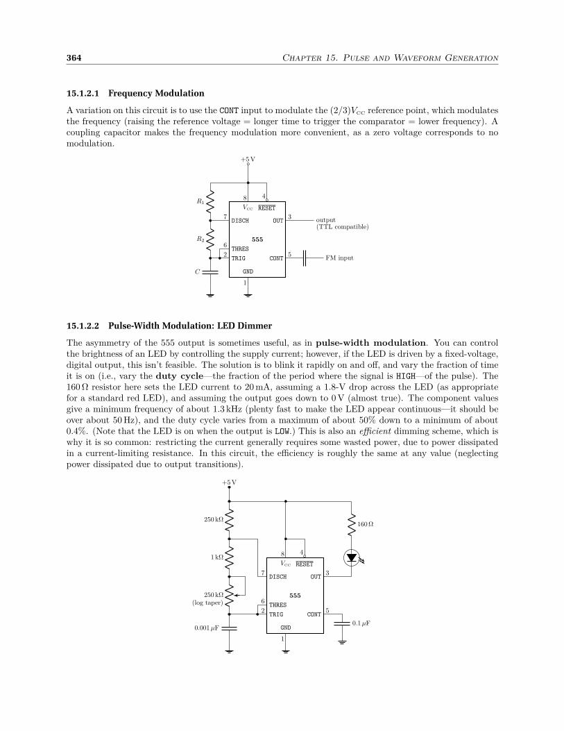
364 Chapter 15. Pulse and Waveform Generation
15.1.2.1 Frequency Modulation
A variation on this circuit is to use the CONT input to modulate the (2/3)VCC reference point, which modulatesthe frequency (raising the reference voltage = longer time to trigger the comparator = lower frequency). Acoupling capacitor makes the frequency modulation more convenient, as a zero voltage corresponds to nomodulation.
555
THRES
TRIG
DISCH OUT
CONT
GND
1
R1
R2
C
7
6
2
3
5FM input
output(TTL compatible)
+5 V
8 4
VCC RESET
15.1.2.2 Pulse-Width Modulation: LED Dimmer
The asymmetry of the 555 output is sometimes useful, as in pulse-width modulation. You can controlthe brightness of an LED by controlling the supply current; however, if the LED is driven by a fixed-voltage,digital output, this isn’t feasible. The solution is to blink it rapidly on and off, and vary the fraction of timeit is on (i.e., vary the duty cycle—the fraction of the period where the signal is HIGH—of the pulse). The160 Ω resistor here sets the LED current to 20 mA, assuming a 1.8-V drop across the LED (as appropriatefor a standard red LED), and assuming the output goes down to 0 V (almost true). The component valuesgive a minimum frequency of about 1.3 kHz (plenty fast to make the LED appear continuous—it should beover about 50 Hz), and the duty cycle varies from a maximum of about 50% down to a minimum of about0.4%. (Note that the LED is on when the output is LOW.) This is also an efficient dimming scheme, which iswhy it is so common: restricting the current generally requires some wasted power, due to power dissipatedin a current-limiting resistance. In this circuit, the efficiency is roughly the same at any value (neglectingpower dissipated due to output transitions).
555
THRES
TRIG
DISCH OUT
CONT
GND
1
+5 V
250 kΩ
1 kΩ
250 kΩ
0.001 µF
(log taper)
7
6
2
3
5
0.1 µF
160 Ω
8 4
VCC RESET
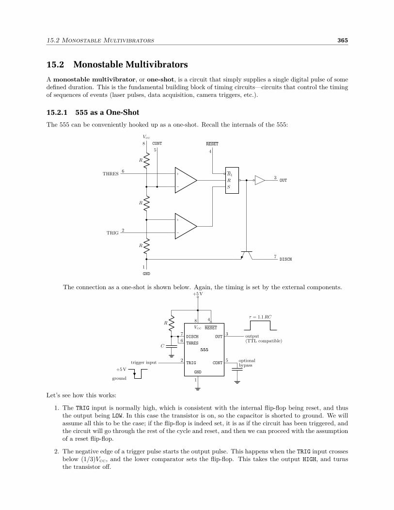
15.2 Monostable Multivibrators 365
15.2 Monostable Multivibrators
A monostable multivibrator, or one-shot, is a circuit that simply supplies a single digital pulse of somedefined duration. This is the fundamental building block of timing circuits—circuits that control the timingof sequences of events (laser pulses, data acquisition, camera triggers, etc.).
15.2.1 555 as a One-Shot
The 555 can be conveniently hooked up as a one-shot. Recall the internals of the 555:
S
R
R1
−
+
−
+
RESET
4
OUT3
R
R
R
THRES6
TRIG2
VCC
8
GND
1
CONT
5
DISCH7
The connection as a one-shot is shown below. Again, the timing is set by the external components.
555
THRES
TRIG
DISCH OUT
CONT
GND
1
R
C
trigger input
7
6
2
3
5 optionalbypass
output(TTL compatible)
+5 V
8 4
VCC RESET
+5 V
ground
τ = 1.1 RC
Let’s see how this works:
1. The TRIG input is normally high, which is consistent with the internal flip-flop being reset, and thusthe output being LOW. In this case the transistor is on, so the capacitor is shorted to ground. We willassume all this to be the case; if the flip-flop is indeed set, it is as if the circuit has been triggered, andthe circuit will go through the rest of the cycle and reset, and then we can proceed with the assumptionof a reset flip-flop.
2. The negative edge of a trigger pulse starts the output pulse. This happens when the TRIG input crossesbelow (1/3)VCC, and the lower comparator sets the flip-flop. This takes the output HIGH, and turnsthe transistor off.

366 Chapter 15. Pulse and Waveform Generation
3. The timing of the output pulse is controlled by charging the capacitor C. The capacitor charges fromVCC via R.
4. The capacitor is uncharged at the beginning of the pulse, and it will charge until the capacitor voltage(and thus THRES input) rises to (2/3)VCC. At this time, the upper comparator resets the flip-flop,ending the pulse and dumping the capacitor charge.
5. Again, we can use the exponential relaxation of the RC circuit to figure out the pulse duration. Thecapacitor voltage rises exponentially (with time RC) from 0 to (2/3)VCC towards VCC. This is equivalentto an exponential decay from VCC towards 0 to (1/3)VCC. Thus we can consider the decay
V (t) = VCC e−t/RC , (15.6)
and if we set V (τ) = (1/3)VCC, where τ is the pulse duration, we get
τ = (log 3)RC ≈ 1.1 RC. (15.7)
Again, “log” here is the natural logarithm, and note that this is independent of the supply voltage.
Note that we have assumed that by the time the flip-flop is reset, the trigger pulse at the TRIG inputis back to HIGH; otherwise the S input to the flip-flop will also be high, putting the flip-flop into the “bad”state. (In reality, typical 555’s will allow the TRIG to override THRES to avoid any such bad states.) Thenet effect is that the output pulse will be “stretched” beyond the RC duration until the trigger input goeshigh. One workaround for this (if you’re stuck with long pulses but want to trigger short pulses) is to runthe trigger input through a differentiator (with a short RC time) and then into the 555.
Also, note that the usual intent of this circuit is to make fairly short (ms-scale) timing pulses, sothat the timing capacitor is typically small (∼µF or smaller). In this case, there is no problem with the555’s transistor effectively shorting the capacitor to dump the charge. However, in the case of a very largecapacitance, especially with a large VCC, the large current that may flow when dumping the capacitor chargecould cause problems, in which case a small current-limiting resistance in the capacitor-DISCH path wouldbe prudent.
15.2.1.1 The 74121
A number of other monostable multivibrators are available, more-or-less prepackaged. A good example isthe 74121, which is faster than the 555 circuit—it can be programmed for pulses down to 35 ns, and up to28 s. The “guts” and some external connections of the 74121 are shown below.
monostable
Q
QA1A2
B
3
4
5
74121
+5 V
14
7
Rint
+5 V
2 kΩ
Rext
+5 V
Cext
10 11 9
Cext Rext/Cext
Some operation notes:
1. As in the 555, the internal monostable is controlled by the time for the external capacitor to chargevia a resistor. The resistor can be internal (Rint) if pin 9 is connected to +5 V , or external, if Rext
is connected between pin 11 and +5 V . (Of course, if both are connected, then we have the parallelresistance of the two.) The pulse duration is given by
τ = (log 2)RC ≈ 0.693 RC. (15.8)

15.3 Circuit Practice 367
2. The internal monostable is triggered by a rising pulse edge, but there is some extra input logic to makethis more flexible. For example, suppose A1 and B are held HIGH. Then a falling edge on A2 triggersthe pulse. Of course, A1 and A2 can be exchanged here.
3. Similarly, if either A1 or A2 are held LOW, then a rising edge into B will trigger the flip-flop. In this case,the B input goes into a Schmitt trigger (0.2-V hysteresis), and thus can handle slow/noisy inputs.
4. The 74121 is nonretriggerable; this means the device will ignore any input edges while it is generatingan output pulse. Other one-shots, like the 74123, is retriggerable, which means that a new triggeringedge will always start a new timing cycle, even if already in the middle of a timing cycle.
15.2.1.2 Combining One-Shots: Pulse Delay
In complex timing systems, where many things must happen at the proper times, many one-shots can bechained together to generate the proper timing sequence. As simple example, two one-shots can be chainedtogether to generate a delayed pulse from an initial trigger pulse. This times two events with a fixed delay,such as launching a projectile, and then a short time later triggering a photographic flash.
monostable monostableQ1 Q2input output
input
Q1
Q2/output
Note the different edge triggers of the two monostables.
15.3 Circuit Practice
15.3.1 Duty-Cycle Control
What is the duty cycle of the basic astable circuit (reproduced below)?
555
THRES
TRIG
DISCH OUT
CONT
GND
1
R1
R2
C
7
6
2
3
5 optionalbypass
output(TTL compatible)
+5 V
8 4
VCC RESET
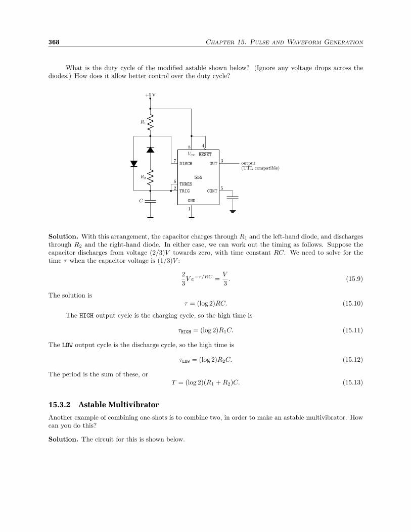
368 Chapter 15. Pulse and Waveform Generation
What is the duty cycle of the modified astable shown below? (Ignore any voltage drops across thediodes.) How does it allow better control over the duty cycle?
555
THRES
TRIG
DISCH OUT
CONT
GND
1
+5 V
R1
R2
C
7
6
2
3
5
output(TTL compatible)
8 4
VCC RESET
Solution. With this arrangement, the capacitor charges through R1 and the left-hand diode, and dischargesthrough R2 and the right-hand diode. In either case, we can work out the timing as follows. Suppose thecapacitor discharges from voltage (2/3)V towards zero, with time constant RC. We need to solve for thetime τ when the capacitor voltage is (1/3)V :
2
3V e−τ/RC =
V
3. (15.9)
The solution isτ = (log 2)RC. (15.10)
The HIGH output cycle is the charging cycle, so the high time is
τHIGH = (log 2)R1C. (15.11)
The LOW output cycle is the discharge cycle, so the high time is
τLOW = (log 2)R2C. (15.12)
The period is the sum of these, orT = (log 2)(R1 + R2)C. (15.13)
15.3.2 Astable Multivibrator
Another example of combining one-shots is to combine two, in order to make an astable multivibrator. Howcan you do this?
Solution. The circuit for this is shown below.
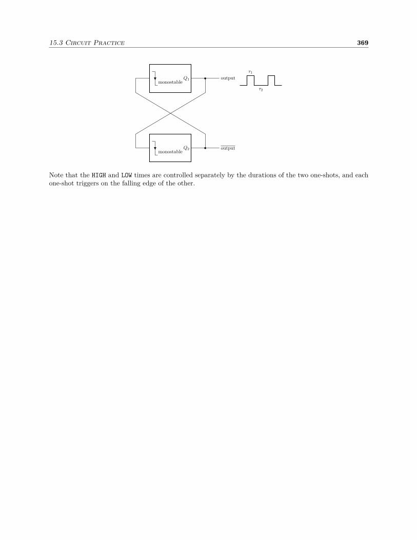
15.3 Circuit Practice 369
monostable
monostable
Q1
Q2
output
output
τ1
τ2
Note that the HIGH and LOW times are controlled separately by the durations of the two one-shots, and eachone-shot triggers on the falling edge of the other.

370 Chapter 15. Pulse and Waveform Generation
15.4 Exercises
Problem 15.1
Shown below is the classic configuration of the 555 timer as an astable multivibrator, except thatwe’re treating the RESET line as an extra input (recall that normally it’s just tied to +5 V for normalastable operation).
555
THRES
TRIG
DISCH OUT
CONT
GND
1
R1
R2
C
7
6
2
3
5 optionalbypass
output(TTL compatible)
+5 V
(new input)+5 V
0 V
8 4
VCC RESET
Describe what happens when the RESET input goes through one HIGH–LOW–HIGH pulse cycle as shown.More specifically, you should say what happens to the OUT line and capacitor voltage on each transition(HIGH–LOW and LOW–HIGH), and what happens after the input pulse is finished.
Note: on the internal flip-flop of the 555, you should assume the R1 input overrides the others.
Problem 15.2
Shown below is (a) the basic 555 astable multivibrator and (b) a modified version. For each circuitcompute the period and duty cycle in terms of R1, R2, C, and any relevant voltages.
555
THRES
TRIG
DISCH OUT
CONT
GND
1
R1
R2
C
7
6
2
3
5
output
+5 V
8 4
VCC RESET
(a)
555
THRES
TRIG
DISCH OUT
CONT
GND
1
R1
R2
C
7
6
2
3
5+4 V
output
+5 V
8 4
VCC RESET
(b)
Problem 15.3
Shown below is a 555-based astable multivibrator with 50% duty cycle. Show that it works as adver-tised, and compute the oscillation period.

15.4 Exercises 371
CMOS 555
THRES
TRIG
DISCH OUT
CONT
GND
1
C
R
7
6
2
3
5
output
+VCC
8 4
VCC RESET
Note: this circuit only works with CMOS variants of the 555 (like the 7555), where the output willswing all the way from ground to +VCC.
Problem 15.4
Suppose you have a standard TTL logic gate, and you want to put a Schmitt trigger on one of theinputs to address a problematic input signal. However, suppose that all you have is a 555; show howto wire a 555 to act as a Schmitt trigger (actually, an inverting Schmitt trigger). Make sure to explainwhy your circuit acts as a Schmitt trigger, and what are the input logic levels.
Problem 15.5
Work out the period of the basic 555 astable multivibrator circuit, but this time account for the voltagedrop Vd across the discharge transistor when it is turned on. That is, the supply voltage should nolonger drop out of the result. Assuming Vd = 0.2 V, how much does this affect the period compared tothe idealized value if VCC = +5 V?
Problem 15.6
In one incarnation, the bicolor LED looks like an ordinary LED (plastic package with two leads),but is really 2 LEDs in parallel, with one reversed. That is, if current flows “forwards,” the LED lightsgreen, and if it flows “backwards,” the LED lights red.
Design a circuit two 555’s to light a bicolor LED, alternating between red and green. For concreteness,design for a ∼50% duty cycle (approximately equal time in each color), with a period of 1 s. Usewhatever passive components you like, but be specific about their values. Also, show all pin connectionson the 555’s.
Hint: note that it would be a bad idea to configure two 555 as independent oscillators. Why? Insteadtry using one of the 555’s as a NOT gate.
Problem 15.7
Design a 10 kHz square-wave oscillator (50% duty cycle) using only 74121’s and capacitors.
Problem 15.8
Show how to build a 4-bit ripple counter (mis)using only 555 chips. (Plus sufficient wire and a +5-Vpower supply; no other components needed/allowed. You may assume the clock signal already exists.)Some notes:

372 Chapter 15. Pulse and Waveform Generation
• Your solution could (should) end up involving a considerable number of 555’s. Stay organized andpresent your solution without drawing out each and every 555 explicitly. Otherwise, use as many555’s as you like—they’re free, at least on paper. Start by figuring out what logic elements you’llneed (gates, flip-flops), and how to repurpose 555’s to make them happen.
• For concreteness of operation, assume the actual 555 involved to be a TLC551. Recall that theinternal flip-flop of this chip deals with potential “bad” inputs by allowing RESET to override TRIG,which can in turn override THRES.
• Be careful with the clock-input operation of the counter; remember that a ripple counter typicallyemploys edge-triggered clock inputs. You may want to seek out (and study!) an example of howclock-edge triggering is implemented in another circuit.

Chapter 16
Digital–Analog Interfaces
One of the most important concepts in digital electronics is interfacing digital circuits to analog circuits. If ananalog signal serves as the input to a digital circuit, then we need analog-to-digital conversion (ADC),while a digital circuit generating an analog signal requires digital-to-analog conversion (DAC). We willconsider the latter first, which is simpler, and ADC often relies on DAC.
16.1 Digital-to-Analog Conversion
Digital-to-analog conversion is very common in everyday circuits. This is required to generate the audiosignals in cell phones and CD/DVD/MP3 players, and to generate the output intensity (or color) of displaysin LCD projectors or in CRT/plasma/LCD displays. Essentially, any analog signal coming out of a computermust have gone through the DAC process.
16.1.1 Resolution
Before understanding how DAC circuitry works, let’s review some of the resolution requirements for repre-senting analog signals. Analog signals must be sampled—that is instead of a continuous function y(t), wemust represent it via samples yj := y(tj) at sample times tj (typically regularly spaced), and the values of yj
must be represented with some finite precision (i.e., it must be represented with a finite number of bits). Interms of amplitude resolution, if there are N bits of data, then there are 2N different signal levels availablewithin a defined range (e.g., within some voltage range). The signal levels could be positive only, representedby unsigned integers, or positive/negative using signed integers (or unsigned integers after adding an offsetthat ensures the signal is always positive). In this case, since the “real” signal must always be rounded to thenearest available level, the fractional sampling resolution is 2−N , and the absolute resolution is 2−N Vrange fora voltage signal if Vrange is the total voltage range available for sampling the signal. Since the rounded valueshould be to the nearest sampling value, the maximum error is 1/2 of the resolution, or 2−(N+1) maximumfractional error for signals within Vrange. So, for 16-bit sampling, the error is at worst about 8 ppm.
In terms of timing resolution, the requirement is set via the sampling theorem. Suppose we samplea signal every ∆t in time. Then the sampling rate is given by
sampling rate =1
∆t. (16.1)
Then we can also define the Nyquist frequency by
Nyquist frequency =1
2∆t=
sampling rate
2. (16.2)
It turns out that, according to the sampling theorem, the Nyquist frequency is the largest frequency that isaccurately reproduced by the sampled signal.1 For example, in compact-disc (CD) audio, the sampling rate
1For details, see Daniel Adam Steck, Quantum and Atom Optics, available online at http://steck.us/teaching.
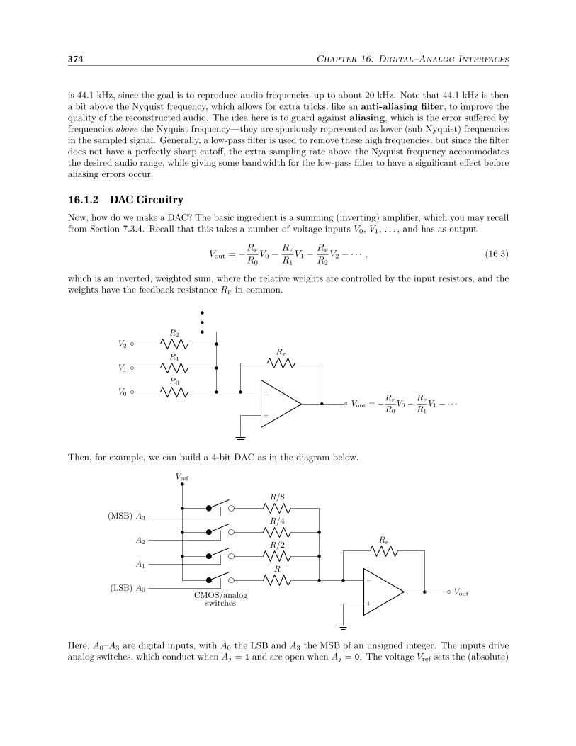
374 Chapter 16. Digital–Analog Interfaces
is 44.1 kHz, since the goal is to reproduce audio frequencies up to about 20 kHz. Note that 44.1 kHz is thena bit above the Nyquist frequency, which allows for extra tricks, like an anti-aliasing filter, to improve thequality of the reconstructed audio. The idea here is to guard against aliasing, which is the error suffered byfrequencies above the Nyquist frequency—they are spuriously represented as lower (sub-Nyquist) frequenciesin the sampled signal. Generally, a low-pass filter is used to remove these high frequencies, but since the filterdoes not have a perfectly sharp cutoff, the extra sampling rate above the Nyquist frequency accommodatesthe desired audio range, while giving some bandwidth for the low-pass filter to have a significant effect beforealiasing errors occur.
16.1.2 DAC Circuitry
Now, how do we make a DAC? The basic ingredient is a summing (inverting) amplifier, which you may recallfrom Section 7.3.4. Recall that this takes a number of voltage inputs V0, V1, . . . , and has as output
Vout = −RF
R0V0 −
RF
R1V1 −
RF
R2V2 − · · · , (16.3)
which is an inverted, weighted sum, where the relative weights are controlled by the input resistors, and theweights have the feedback resistance RF in common.
−
+
Vout = −RF
R0V0 −
RF
R1V1 − · · ·
RF
R0
V0
R1
V1
R2
V2
Then, for example, we can build a 4-bit DAC as in the diagram below.
−
+
Vout
RF
R
R/2
R/4
R/8
Vref
(LSB) A0
A1
A2
(MSB) A3
CMOS/analogswitches
Here, A0–A3 are digital inputs, with A0 the LSB and A3 the MSB of an unsigned integer. The inputs driveanalog switches, which conduct when Aj = 1 and are open when Aj = 0. The voltage Vref sets the (absolute)

16.1 Digital-to-Analog Conversion 375
voltage resolution and the range of the conversion. Then using the summing-amp formula,
Vout = −A0RF
RVref − 2A1
RF
RVref − 4A2
RF
RVref − 8A3
RF
RVref
= −RF
RVref
(
A020 + A121 + A222 + A323)
.
(16.4)(DAC output)
So, for example, an input of 0011 corresponds to Vout = −3(RF/R)Vref . Of course, usually we want a positive
output, which requires another inverting amplifier.
16.1.3 R–2R Ladder
One problem with the above circuit is that it requires a series of resistors of different values to be madeto high accuracy, which is difficult, especially for a high-resolution DAC. It is much easier to make sets ofmatching resistors, and there is a circuit that takes advantage of this, called the R–2R ladder, which usesonly resistors of size R and 2R. The idea is below.
−
+
Vout
RF
R
R
R
2R
2R
2R
2R
2R
A3
A2
A1
A0
Vref
Again, the inputs are A0–A3 here, controlling analog/CMOS switches (here SPDT). To see how this works,consider the Thévenin-equivalent circuit for the A0 input. This is a simple 50% voltage divider, so theequivalent resistance is R, and the voltage is half the input A0Vref . (Note that we consider A0 = 0 if theswitch is down, A0 = 1 if the switch is up.)
2R
V0 = A0Vref
2R =V0
2
R
Now lumping this equivalent circuit into the next “stage” with the A1 input, we have a similar voltage-dividersituation.

376 Chapter 16. Digital–Analog Interfaces
2R
V1 = A1Vref
2R
V0/2
=
(
V0
4+
V1
2
) R
Note that the Thévenin-equivalent voltage is just the average of the two input voltages. Continuing thisprocess, we find that at each stage we add in half of the next input voltage and divide the remaining onesby two. The result is
Vout = −VrefRF
R
(
A0
16+
A1
4+
A2
8+
A3
2
)
= −VrefRF
24R
(
A020 + A121 + A222 + A323)
.
(16.5)(output of R–2R ladder)
Thus, up to an overall factor, we obtain the same output as in Eq. (16.4).
16.2 Analog-to-Digital Conversion
The complementary process to digital-to-analog conversion is analog-to-digital conversion (ADC). Wewill go through several ADC methods.
16.2.1 Flash ADC
A conceptually simple method for ADC is flash ADC or parallel-encoding ADC. The idea is to use avoltage-divider chain to create many reference voltage, and a separate comparator is used to compare theinput voltage to each reference. Then output logic is needed to properly encode the digital output as abinary number. As a simple example, consider the 2-bit flash ADC below.
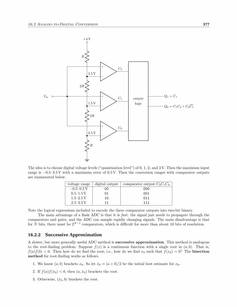
16.2 Analog-to-Digital Conversion 377
output
logic−
+
−
+
−
+
C2
C1
C0
R
+4 V
2R
2R
R
2.5 V
1.5 V
0.5 V
Vin Q1 = C1
Q0 = C1C2 + C0C1
The idea is to choose digital voltage levels (“quantization level”) of 0, 1, 2, and 3 V. Then the maximum inputrange is −0.5–3.5 V with a maximum error of 0.5 V. Then the conversion ranges with comparator outputsare enumerated below.
voltage range digital output comparator output C2C1C0
−0.5–0.5 V 00 000
0.5–1.5 V 01 001
1.5–2.5 V 10 011
2.5–3.5 V 11 111
Note the logical expressions included to encode the three comparator outputs into two-bit binary.The main advantage of a flash ADC is that it is fast: the signal just needs to propagate through the
comparators and gates, and the ADC can sample rapidly changing signals. The main disadvantage is thatfor N bits, there must be 2N−1 comparators, which is difficult for more than about 10 bits of resolution.
16.2.2 Successive Approximation
A slower, but more generally useful ADC method is successive approximation. This method is analogousto the root-finding problem: Suppose f(x) is a continuous function with a single root in (a, b). That is,f(a)f(b) < 0. Then how do we find the root; i.e., how do we find x0 such that f(x0) = 0? The bisectionmethod for root-finding works as follows.
1. We know (a, b) brackets x0. So let x0 = (a + b)/2 be the initial best estimate for x0.
2. If f(a)f(x0) < 0, then (a, x0) brackets the root.
3. Otherwise, (x0, b) brackets the root.
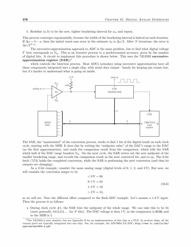
378 Chapter 16. Digital–Analog Interfaces
4. Redefine (a, b) to be the new, tighter bracketing interval for x0, and repeat.
This process converges exponentially, because the width of the bracketing interval is halved on each iteration.If ∆x = b − a, then the initial worst-case error in the estimate x0 is ∆x/2. After N iterations, the error is∆x/2N+1.
The successive-approximation approach to ADC is the same problem, but to find what digital voltageV best corresponds to Vin. This is an iterative process to a predetermined accuracy, given by the numberof digital bits. A circuit to implement this procedure is shown below. This uses the 74LS503 successive-approximation register (SAR),2
which controls the bisection process. Most ADCs nowadays using successive approximation have allthese components integrated into a single chip, with serial data output—handy for keeping pin counts low,but it’s harder to understand what is going on inside.
AD557DAC
74HCT5748-bit
register
D Q
>
CLK
74LS503 SAR
>
CLK
clock in
−
+
311
VCC
VEE
analog in
/8
/8
/ 8
1 kΩ
+5 V
The SAR, the “mastermind” of the conversion process, works to find 1 bit of the digital result on each clockcycle, starting with the MSB. It does this by writing the “midpoint value” of the DAC’s range to the DAC(as the first approximation), and reads the comparison result from the comparator, which tells the SARwhich half of the DAC range brackets Vin. On the next cycle, the SAR writes out the new midpoint of thesmaller bracketing range, and records the comparison result as the next converted bit, and so on. The 8-bitlatch (’574) holds the completed conversion, while the SAR is performing the next conversion (and thus itsoutputs are changing).
As a 2-bit example, consider the same analog range (digital levels of 0, 1, 2, and 3 V). But now, wewill consider the conversion ranges to be
< 0 V = 00
0–1 V = 01
1–2 V = 10
> 2 V = 11,
(16.6)
as we will see. Note the different offset compared to the flash-ADC example. Let’s assume a 1.3-V input.Then the process is as follows:
• During clock cycle #1, the SAR tries the midpoint of the whole range. We can take this to be 01
(more generally, 0111111. . . for N bits). The DAC voltage is then 1 V, so the comparator is HIGH, andso the MSB is 1.
2The 74LS503 is now obsolete, but see Appendix B for an implementation of this chip in a PLD. In modern chips, all thevarious parts are typically integrated into one chip. See, for example, the ADC0804 SA-ADC: http://www.ti.com/lit/ds/
symlink/adc0804-n.pdf.

16.2 Analog-to-Digital Conversion 379
• During clock cycle #2, the SAR tries the midpoint of the remaining range (10–11). The “midpoint”is 10. The DAC voltage is then 2 V, so the comparator is now LOW, and so the LSB is 0.
Thus, the converted result is 10, in agreement with the table above.The advantages of SA-ADC is that the timing is guaranteed (measured in clock cycles), the result can
be very accurate (if a good DAC is used), and the circuit is not too complicated. The main disadvantage arethat SA-ADC is slower than flash conversion, and thus may need a sample/hold circuit to deal with rapidlychanging input signals.
16.2.3 Single/Dual-Slope ADC
Another pair of important ADC methods goes under the name(s) of single/dual-slope ADC. The ba-sic idea in single-slope ADC is to use a constant-current source to charge a capacitor, and then use acounter/clock combination to measure the time for the capacitor voltage to reach the input Vin.
Dto„oVin
VC
t
The charge time is then proportional to the voltage. The idea is that time is very easy to measure accuratelyand precisely, so the method can be very accurate.
To show this mathematically, consider the capacitor-charging situation diagramed below, where aconstant-current source I charges a capacitor to voltage VC(t).
C
VC
(const) I
Then using Q = CVC and differentiating,
I =dQ
dt= C
dVC
dt, (16.7)
so that for constant I,
VC(t) =It
C. (16.8)
Since I/C is a constant, this can be calibrated precisely to yield VC (and thus Vin) in terms of t.In dual-slope ADC, the conversion is done in two steps.
1. C is charged for a fixed time τ by a constant current I ∝ Vin. If we let α be constant, then we canwrite I = αVin, so that
VC(τ) =αVinτ
C. (16.9)
2. Then, C is discharged at a constant current I ′, and the discharge time δt is measured. Then thedischarge time is fixed as in single-slope ADC by
VC(τ) =I ′δt
C. (16.10)
Thus,
δt =CVC(τ)
I ′=
C(αVinτ/C)
I ′=(ατ
I ′
)
Vin. (16.11)

380 Chapter 16. Digital–Analog Interfaces
In this way, we are left to calibrate ατ/I ′, which is a combination of the output of a current source (α),a time τ , and a current I ′, all of which can be well-calibrated. Notably, the capacitance C dropped out;capacitances are difficult to fabricate in a way that is accurate and stable. Also, note that the first stagetakes time τ , which has an averaging effect over noise in Vin, whereas single-slope conversion is more apt totrigger early on a downward noise fluctuation of Vin.
16.3 Circuit Practice
16.3.1 Computer-Interface DAC Controller
For circuit practice, see the DAC controller board design by Todd Meyrath and Florian Schreck.3 Tracethrough the circuit and note the following.
• The DAC7744 chips have 4 analog outputs, for 8 total output channels per board.
• An 8-bit address bus selects which DAC and output to use. The two LSBs (bits 0 and 1) select whichoutput on a particular chip, bit 2 selects which of the two DACs on the board to activate, and theother bits select which (of possibly many) boards to address. Trace through the logic leading up toand including the NAND gates to verify that it works as advertised.
• This allows only one 16-bit data bus to feed all the outputs. The desired output is selected, the desireddata is presented to the data bus, and then a strobe signal causes the addressed DAC to latch thedesired output value.
• Note that the strobe pulse, which just amounts to matching the proper address, must be delayed behindthe data and address signals so the inputs are settled before “load DAC” is triggered. The pulse isdelayed by a buffered, RC circuit.
• Note that the NOT gates have Schmitt-trigger inputs. What part of the circuit justifies having Schmitt-input NOTs?
16.3.2 3-Bit ADC
Suppose you have a 3-bit DAC, with voltage levels 0 V, 0.1 V, 0.2 V, . . . , in a successive-approximation ADC.If Vin = 0.35 V,
• make a plot of the DAC output vs. time
• what is the final, converted digital value?
Solution. For the converted digital value: 100. The comparison voltages will be: 0.3 V, 0.5 V, 0.4 V.
3http://strontiumbec.com/Control/DAC.pdf, in particular the schematic on p. 13.

16.4 Exercises 381
16.4 Exercises
Problem 16.1
(a) Derive an expression for the dynamic range (the largest vs. the smallest nonzero-amplitude signal)of an N -bit sampled signal. Recall that when you compare two amplitudes A and A0 in dB, theexpression is
(ratio in dB) = 20 log10
(
A
A0
)
(16.12)
(b) What is the dynamic range for CD audio (16 bits) in dB? Bluray audio (24 bits)? (For comparison,the dynamic range of human hearing is usually quoted as 120 dB.)
Problem 16.2
A 3-bit flash ADC uses 7 comparators to compare an input voltage to a set of voltages from a voltage-divider chain (say, 0.5 V, 1.5 V, . . . , 6.5 V).
(a) Describe the possible values for the comparator outputs C6 · · ·C1C0. (C0 does the comparison to0.5 V, and C6 handles the comparison to 6.5 V.)
(b) Give logic expressions required to transform the comparator output C6 · · ·C1C0 into a 3-bit binarynumber (ranging from 000 to represent 0 V and 111 for 7 V). Try to end up with reasonably simplefinal expressions.
Problem 16.3
Use a counter to design a simple DAC based on pulse-width modulation as follows: Your circuit shouldtake an 8-bit digital input, representing an 8-bit unsigned integer, and then control the brightness ofan LED to be proportional to this integer. Assume the clock signal to be given and to be as fast as youneed it to be. You may use whatever support logic you like, but you may find it useful to use a flip-flop,and look into the binary magnitude comparator (read up on the 74688). Make sure to properly limitthe LED current.
Be specific about any ICs you use (i.e., give the model number, like 74688, and if it matters, specifywhich logic family, e.g., 74HCT688). You should show all important connections, but don’t botherwith universal stuff like power supplies, grounds, chip enables, etc. Also, you don’t need to explicitlyshow the clock source, just indicate the existence of the clock signal and show any connections whereit enters your circuit.
Problem 16.4
(a) Use a counter (specifically, an 8-bit up counter), a clock source (astable multivibrator), a compara-tor, and a DAC to design a simple ADC. That is, the counter should count upwards starting from zero,and freeze at the appropriate conversion value (i.e., the frozen counter is the output). Use whateversupport logic you like, and don’t worry about latching the output. You should include a start/resetinput that resets the counter and allows the next conversion to start.
As in Problem 2, be specific about any ICs you use; show all important connections, but don’t botherwith universal stuff; and you don’t need to explicitly show the clock source, just indicate the existenceof the clock signal and show any connections where it enters your circuit.
(b) Why is this ADC slower than a successive-approximation ADC? (And by how much is this ADCslower on average?)
(c) What kind of “bias” does this ADC have in terms of converting a noisy input signal?

382 Chapter 16. Digital–Analog Interfaces
Problem 16.5
(a) In the successive-approximation ADC examples from Section 16.2.2, the convention is that the SARstarts with the “midpoint” word 01111111 for an 8-bit ADC (as in the 74LS502 and 74LS503 SAR’sin Appendix B). Another possible (and reasonable) convention is to start off with the the alternate
midpoint word 10000000. Briefly describe the difference in the end result of the two schemes for anarbitrary input.
(b) Consider the ADC circuit shown below, where the DAC conversion levels are 0, 0.01, 0.02, . . . ,2.55 V. Suppose the input analog voltage of 0.45 V, and as mentioned the SAR starts with 01111111
on the first clock cycle (the “start” cycle). What is the SAR output after 3 more clock cycles?
AD557DAC
161
8
LEDs
74LS503 SAR
>
CLK
clock in
9
START
10
7
8E1
D CC
3 4 5 6 11 12 13 14Q0 Q7
−
+
311
VCC
VEE
10 kΩ
input
VCC (+5 V)
16
2
VCC (+5 V)
470 Ω
/8
/8
/ 8
1 kΩ
+5 V4.7 MΩ
72
3
8
4
Problem 16.6
In this problem, you should design a 2-bit successive-approximation register (SAR), with data (D) andstart-LOW (S) inputs, Q1 (MSB) and Q0 (LSB) outputs, and conversion-complete-LOW (CC) output. Onstart, the outputs should initialize to Q1Q0CC = 011.
(a) Draw a state diagram for the SAR, enumerating all possible output states Q1Q0CC as nodes. Specifyall possible transitions, and label transition arrows with the appropriate input states wherever multipletransitions are possible. Also, make sure to handle all possible states and eliminate the possibility thatthe state machine will get “stuck.” (Remember you can use “X” for “doesn’t matter” for logic states indiagrams and truth tables.)
A suggested template for your state diagram is shown below. (That is, these are the states, you shouldfill in the transitions.)
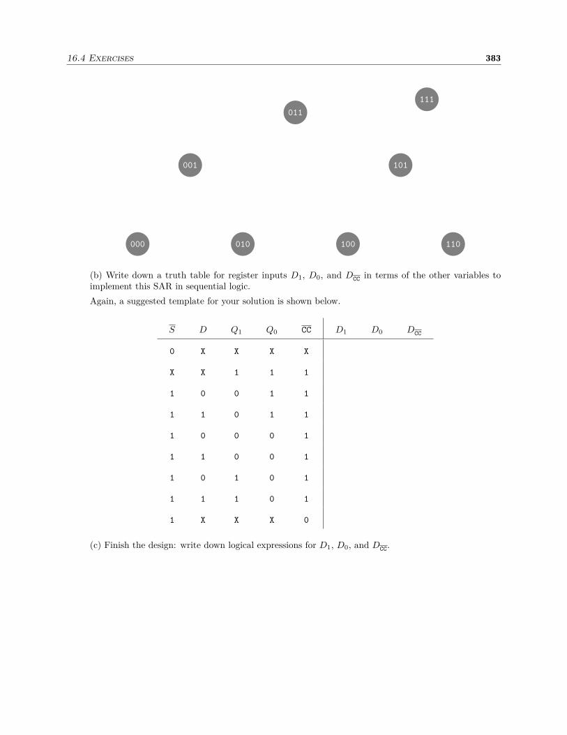
16.4 Exercises 383
011
001 101
000 010 100 110
111
(b) Write down a truth table for register inputs D1, D0, and DCC in terms of the other variables toimplement this SAR in sequential logic.
Again, a suggested template for your solution is shown below.
S D Q1 Q0 CC D1 D0 DCC
0 X X X X
X X 1 1 1
1 0 0 1 1
1 1 0 1 1
1 0 0 0 1
1 1 0 0 1
1 0 1 0 1
1 1 1 0 1
1 X X X 0
(c) Finish the design: write down logical expressions for D1, D0, and DCC.

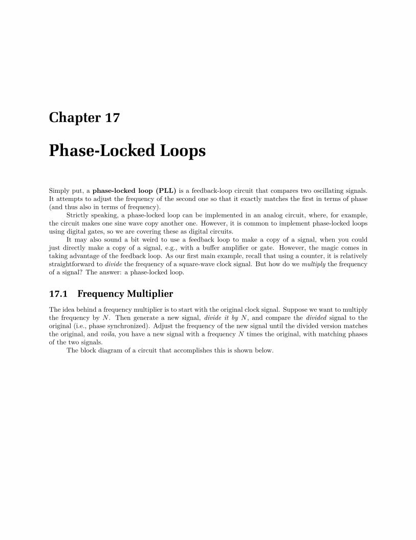
Chapter 17
Phase-Locked Loops
Simply put, a phase-locked loop (PLL) is a feedback-loop circuit that compares two oscillating signals.It attempts to adjust the frequency of the second one so that it exactly matches the first in terms of phase(and thus also in terms of frequency).
Strictly speaking, a phase-locked loop can be implemented in an analog circuit, where, for example,the circuit makes one sine wave copy another one. However, it is common to implement phase-locked loopsusing digital gates, so we are covering these as digital circuits.
It may also sound a bit weird to use a feedback loop to make a copy of a signal, when you couldjust directly make a copy of a signal, e.g., with a buffer amplifier or gate. However, the magic comes intaking advantage of the feedback loop. As our first main example, recall that using a counter, it is relativelystraightforward to divide the frequency of a square-wave clock signal. But how do we multiply the frequencyof a signal? The answer: a phase-locked loop.
17.1 Frequency Multiplier
The idea behind a frequency multiplier is to start with the original clock signal. Suppose we want to multiplythe frequency by N . Then generate a new signal, divide it by N , and compare the divided signal to theoriginal (i.e., phase synchronized). Adjust the frequency of the new signal until the divided version matchesthe original, and voila, you have a new signal with a frequency N times the original, with matching phasesof the two signals.
The block diagram of a circuit that accomplishes this is shown below.
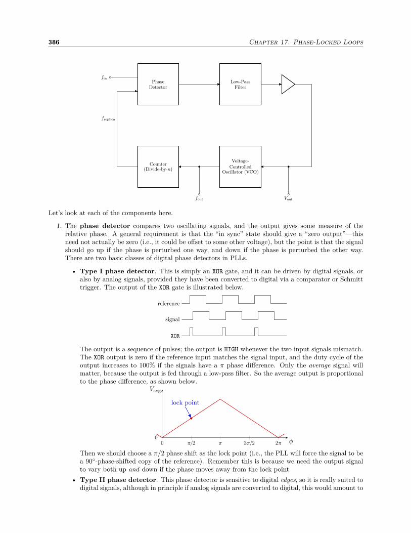
386 Chapter 17. Phase-Locked Loops
PhaseDetector
Low-PassFilter
Counter(Divide-by-n)
Voltage-Controlled
Oscillator (VCO)
fin
freplica
Voutfout
Let’s look at each of the components here.
1. The phase detector compares two oscillating signals, and the output gives some measure of therelative phase. A general requirement is that the “in sync” state should give a “zero output”—thisneed not actually be zero (i.e., it could be offset to some other voltage), but the point is that the signalshould go up if the phase is perturbed one way, and down if the phase is perturbed the other way.There are two basic classes of digital phase detectors in PLLs.
• Type I phase detector. This is simply an XOR gate, and it can be driven by digital signals, oralso by analog signals, provided they have been converted to digital via a comparator or Schmitttrigger. The output of the XOR gate is illustrated below.
reference
signal
XOR
The output is a sequence of pulses; the output is HIGH whenever the two input signals mismatch.The XOR output is zero if the reference input matches the signal input, and the duty cycle of theoutput increases to 100% if the signals have a π phase difference. Only the average signal willmatter, because the output is fed through a low-pass filter. So the average output is proportionalto the phase difference, as shown below.
lock point
Vavg
f0 p/2 p 3p/2 2p0
Then we should choose a π/2 phase shift as the lock point (i.e., the PLL will force the signal to bea 90-phase-shifted copy of the reference). Remember this is because we need the output signalto vary both up and down if the phase moves away from the lock point.
• Type II phase detector. This phase detector is sensitive to digital edges, so it is really suited todigital signals, although in principle if analog signals are converted to digital, this would amount to
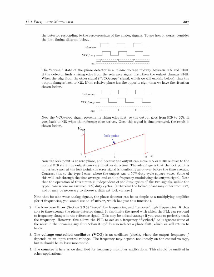
17.1 Frequency Multiplier 387
the detector responding to the zero-crossings of the analog signals. To see how it works, considerthe first timing diagram below.
reference
VCO/copy
out
The “normal” state of the phase detector is a middle voltage midway between LOW and HIGH.If the detector finds a rising edge from the reference signal first, then the output changes HIGH.When the edge from the other signal (“VCO/copy” signal, which we will explain below), then theoutput changes back to MID. If the relative phase has the opposite sign, then we have the situationshown below.
reference
VCO/copy
out
Now the VCO/copy signal presents its rising edge first, so the output goes from MID to LOW. Itgoes back to MID when the reference edge arrives. Once this signal is time-averaged, the result isshown below.
lock point
Vavg
f0-p +p
0
Now the lock point is at zero phase, and because the output can move LOW or HIGH relative to thenormal MID state, the output can vary in either direction. The advantage is that the lock point isin perfect sync: at the lock point, the error signal is identically zero, ever before the time average.Contrast this to the type-I case, where the output was a 50%-duty-cycle square wave. Some ofthis will leak through the time average, and end up frequency-modulating the output signal. Notethat the operation of this circuit is independent of the duty cycles of the two signals, unlike thetype-I case where we assumed 50% duty cycles. (Otherwise the locked phase may differ from π/2,and it may be necessary to choose a different lock voltage.)
Note that for sine-wave analog signals, the phase detector can be as simple as a multiplying amplifier(for rf frequencies, you would use an rf mixer, which has just this function).
2. The low-pass filter (Section 2.3.5) “keeps” low frequencies, and “removes” high frequencies. It thusacts to time-average the phase-detector signal. It also limits the speed with which the PLL can respondto frequency changes in the reference signal. This may be a disadvantage if you want to perfectly trackthe frequency. However, this allows the PLL to act as a frequency “flywheel,” so it ignores some ofthe noise in the incoming signal to “clean it up.” It also induces a phase shift, which we will return tobelow.
3. The voltage-controlled oscillator (VCO) is an oscillator (clock), where the output frequency fdepends on an input control voltage. The frequency may depend nonlinearly on the control voltage,but it should be at least monotonic.
4. The counter is here as we described for frequency-multiplier applications. This should be omitted inother applications.
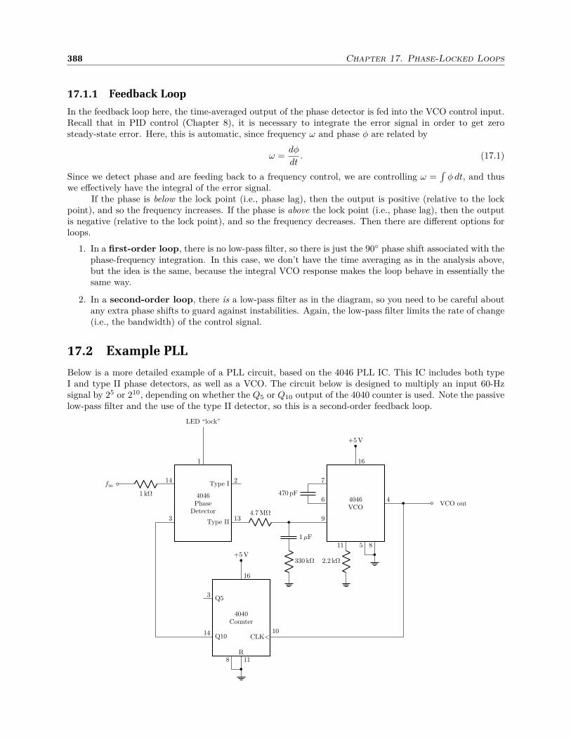
388 Chapter 17. Phase-Locked Loops
17.1.1 Feedback Loop
In the feedback loop here, the time-averaged output of the phase detector is fed into the VCO control input.Recall that in PID control (Chapter 8), it is necessary to integrate the error signal in order to get zerosteady-state error. Here, this is automatic, since frequency ω and phase φ are related by
ω =dφ
dt. (17.1)
Since we detect phase and are feeding back to a frequency control, we are controlling ω =∫
φ dt, and thuswe effectively have the integral of the error signal.
If the phase is below the lock point (i.e., phase lag), then the output is positive (relative to the lockpoint), and so the frequency increases. If the phase is above the lock point (i.e., phase lag), then the outputis negative (relative to the lock point), and so the frequency decreases. Then there are different options forloops.
1. In a first-order loop, there is no low-pass filter, so there is just the 90 phase shift associated with thephase-frequency integration. In this case, we don’t have the time averaging as in the analysis above,but the idea is the same, because the integral VCO response makes the loop behave in essentially thesame way.
2. In a second-order loop, there is a low-pass filter as in the diagram, so you need to be careful aboutany extra phase shifts to guard against instabilities. Again, the low-pass filter limits the rate of change(i.e., the bandwidth) of the control signal.
17.2 Example PLL
Below is a more detailed example of a PLL circuit, based on the 4046 PLL IC. This IC includes both typeI and type II phase detectors, as well as a VCO. The circuit below is designed to multiply an input 60-Hzsignal by 25 or 210, depending on whether the Q5 or Q10 output of the 4040 counter is used. Note the passivelow-pass filter and the use of the type II detector, so this is a second-order feedback loop.
4046Phase
Detector
4046VCO
4040Counter
LED “lock”
1
1 kΩ
fin14
3
2
13
Type I
Type II
4.7 MΩ
1 µF
330 kΩ
9
6
7
470 pF
11
2.2 kΩ
5 8
+5 V
16
VCO out4
CLK<10
16
+5 V
8 11R
Q5
Q10
3
14
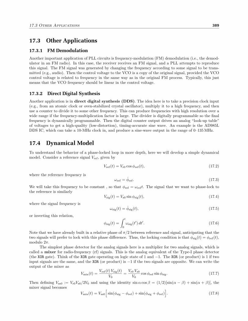
17.3 Other Applications 389
17.3 Other Applications
17.3.1 FM Demodulation
Another important application of PLL circuits is frequency-modulation (FM) demodulation (i.e., the demod-ulator in an FM radio). In this case, the receiver receives an FM signal, and a PLL attempts to reproducethis signal. The FM signal was generated by changing the frequency according to some signal to be trans-mitted (e.g., audio). Then the control voltage to the VCO is a copy of the original signal, provided the VCOcontrol voltage is related to frequency in the same way as in the original FM process. Typically, this justmeans that the VCO frequency should be linear in the control voltage.
17.3.2 Direct Digital Synthesis
Another application is in direct digital synthesis (DDS). The idea here is to take a precision clock input(e.g., from an atomic clock or oven-stabilized crystal oscillator), multiply it to a high frequency, and thenuse a counter to divide it to some other frequency. This can produce frequencies with high resolution over awide range if the frequency-multiplication factor is large. The divider is digitally programmable so the finalfrequency is dynamically programmable. Then the digital counter output drives an analog “look-up table”of voltages to get a high-quality (low-distortion), timing-accurate sine wave. An example is the AD985LDDS IC, which can take a 10-MHz clock in, and produce a sine-wave output in the range of 0–135 MHz.
17.4 Dynamical Model
To understand the behavior of a phase-locked loop in more depth, here we will develop a simple dynamicalmodel. Consider a reference signal Vref , given by
Vref(t) = Vr0 cos φref(t), (17.2)
where the reference frequency isωref = φref . (17.3)
We will take this frequency to be constant , so that φref = ωreft. The signal that we want to phase-lock tothe reference is similarly
Vsig(t) = Vs0 sin φsig(t), (17.4)
where the signal frequency isωsig(t) = φsig(t), (17.5)
or inverting this relation,
φsig(t) =
∫ t
0
ωsig(t′) dt′. (17.6)
Note that we have already built in a relative phase of π/2 between reference and signal, anticipating that thetwo signals will prefer to lock with this phase difference. Thus, the locking condition is that φsig(t) = φref(t),modulo 2π.
The simplest phase detector for the analog signals here is a multiplier for two analog signals, which iscalled a mixer for radio-frequency (rf) signals. This is the analog equivalent of the Type-I phase detector(the XOR gate). Think of the XOR gate operating on logic state of 1 and −1. The XOR (or product) is 1 if twoinput signals are the same, and the XOR (or product) is −1 if the two signals are opposite. We can write theoutput of the mixer as
Vmix(t) =Vref(t) Vsig(t)
V0=
Vr0 Vs0
V0cos φref sin φsig. (17.7)
Then defining Vm0 := Vr0Vs0/2V0 and using the identity sin α cos β = (1/2)[sin(α − β) + sin(α + β)], themixer signal becomes
Vmix(t) = Vm0
[
sin(φsig − φref) + sin(φsig + φref)]
. (17.8)

390 Chapter 17. Phase-Locked Loops
In phase-locked-loop operation, only the first term will be important here. At or near the locking condition,ωsig ≈ ωref , so the first term varies slowly (close to dc), while the second term has a frequency of ωsig +ωref ≈2ωref , which is much faster. The effect of this fast oscillation will tend to be averaged away to zero, especiallyas we will be feeding this mixer signal through a low-pass filter, which will greatly suppress the second term.Thus, we will write
Vmix(t) = Vm0 sin(φsig − φref), (17.9)
as far as the operation of the feedback loop is concerned.To complete the loop, we must connect the output of the mixer to the input of the VCO, via a low-pass
filter (to make a second-order loop). Then the VCO outputs a signal at frequency
ωsig(t) = ωs0 −gI
Vm0
∫ t
0
Vmix(t′) dt′, (17.10)
where ωs0 is the “natural” frequency of the VCO (i.e., the frequency with zero input voltage), gI is an“integral” gain factor, and we are modeling the low-pass filter via an integral (recalling from Section 2.2.1that a low-pass filter acts as an integrator provided the output signal is small compared to the input). Notethat we have included a minus sign here to provide negative feedback. However, this is optional, but withoutit the relative phase at the lock point will differ by π from the analysis here.
17.4.1 Equation of Motion
Now we can write down a dynamical equation for the phase-locked loop. Consider the phase difference
∆φ(t) := φsig(t)− φref . (17.11)
The first derivative gives the frequency difference
∆φ(t) = ωsig(t)− ωref . (17.12)
Putting in Eq. (17.10) for ωsig,
∆φ(t) = ωs0 − ωref −gI
Vm0
∫ t
0
Vmix(t′) dt′. (17.13)
Differentiating this equation,
∆φ(t) = − gI
Vm0Vmix(t), (17.14)
and then using Eq. (17.9), the result is
∆φ(t) = −gI sin(∆φ). (17.15)
This equation has the form of a mechanical pendulum, θ = −(g/ℓ) sin θ. This means that ∆φ = 0 (modulo2π) is a steady state, meaning that once locked, the circuit can stay locked. However, there is no means tobecome locked: if the relative phase is displaced from the lock point, it will oscillate back and forth about itwithout settling. Thus, we need to introduce some damping.
17.4.2 Damping
To introduce damping, we will introduce a “proportional” term in the feedback in Eq. (17.13):
∆φ(t) = ωs0 − ωref −gI
Vm0
∫ t
0
Vmix(t′) dt′ − gP
Vm0Vmix(t). (17.16)
Here gP is the “proportional” gain. This model corresponds to the two-resistor, one-capacitor filter in theexample PLL circuit on p. 388. At low frequencies, the filter acts as an ordinary low-pass filter (integrator),while at high frequencies the capacitor acts as a short, so the two resistors form a divider that determine gP.
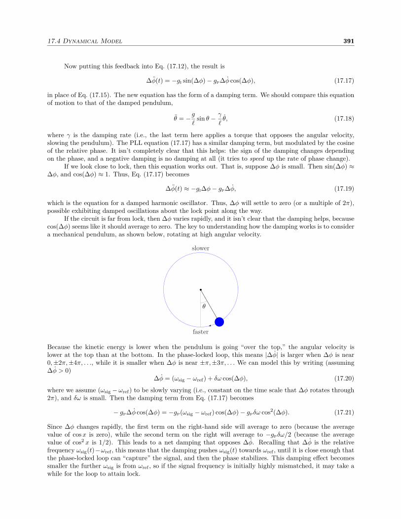
17.4 Dynamical Model 391
Now putting this feedback into Eq. (17.12), the result is
∆φ(t) = −gI sin(∆φ)− gP∆φ cos(∆φ), (17.17)
in place of Eq. (17.15). The new equation has the form of a damping term. We should compare this equationof motion to that of the damped pendulum,
θ = −g
ℓsin θ − γ
ℓθ, (17.18)
where γ is the damping rate (i.e., the last term here applies a torque that opposes the angular velocity,slowing the pendulum). The PLL equation (17.17) has a similar damping term, but modulated by the cosineof the relative phase. It isn’t completely clear that this helps: the sign of the damping changes dependingon the phase, and a negative damping is no damping at all (it tries to speed up the rate of phase change).
If we look close to lock, then this equation works out. That is, suppose ∆φ is small. Then sin(∆φ) ≈∆φ, and cos(∆φ) ≈ 1. Thus, Eq. (17.17) becomes
∆φ(t) ≈ −gI∆φ− gP∆φ, (17.19)
which is the equation for a damped harmonic oscillator. Thus, ∆φ will settle to zero (or a multiple of 2π),possible exhibiting damped oscillations about the lock point along the way.
If the circuit is far from lock, then ∆φ varies rapidly, and it isn’t clear that the damping helps, becausecos(∆φ) seems like it should average to zero. The key to understanding how the damping works is to considera mechanical pendulum, as shown below, rotating at high angular velocity.
θ
faster
slower
Because the kinetic energy is lower when the pendulum is going “over the top,” the angular velocity islower at the top than at the bottom. In the phase-locked loop, this means |∆φ| is larger when ∆φ is near0,±2π,±4π, . . ., while it is smaller when ∆φ is near ±π,±3π, . . . We can model this by writing (assuming∆φ > 0)
∆φ = (ωsig − ωref) + δω cos(∆φ), (17.20)
where we assume (ωsig −ωref) to be slowly varying (i.e., constant on the time scale that ∆φ rotates through2π), and δω is small. Then the damping term from Eq. (17.17) becomes
− gP∆φ cos(∆φ) = −gP(ωsig − ωref) cos(∆φ)− gPδω cos2(∆φ). (17.21)
Since ∆φ changes rapidly, the first term on the right-hand side will average to zero (because the averagevalue of cos x is zero), while the second term on the right will average to −gPδω/2 (because the averagevalue of cos2 x is 1/2). This leads to a net damping that opposes ∆φ. Recalling that ∆φ is the relativefrequency ωsig(t)−ωref , this means that the damping pushes ωsig(t) towards ωref , until it is close enough thatthe phase-locked loop can “capture” the signal, and then the phase stabilizes. This damping effect becomessmaller the further ωsig is from ωref , so if the signal frequency is initially highly mismatched, it may take awhile for the loop to attain lock.
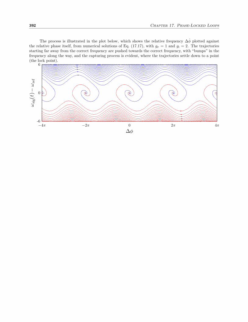
392 Chapter 17. Phase-Locked Loops
The process is illustrated in the plot below, which shows the relative frequency ∆φ plotted againstthe relative phase itself, from numerical solutions of Eq. (17.17), with gP = 1 and gI = 2. The trajectoriesstarting far away from the correct frequency are pushed towards the correct frequency, with “bumps” in thefrequency along the way, and the capturing process is evident, where the trajectories settle down to a point(the lock point).
Df
0 2p-2p 4p-4p
wsigo(t
)oo-
oowref
6
-6
0

17.5 Exercises 393
17.5 Exercises
Problem 17.1
Recall that a phase-locked loop based on a Type I detector is sensitive to the duty cycle of the inputsignal.
(a) Briefly, why?
(b) Suppose you have a signal consisting of a train of (digital) pulses. The rising edges occur atregularly, at a well-defined frequency. The falling edges, however, occur at irregular times. Show(draw a schematic and describe your reasoning) how to use two flip-flops (pick your favoritetype) as divide-by-2 counters with a phase-locked loop to create a “cleaned” version of the same signal(i.e., square wave, 50% duty cycle, same frequency as the rising edges, “ignores” the falling edges).Note that the actual output may be phase-shifted compared to what is shown here.
what you want (up to a phase shift):
what you’ve got:
You can use the following schematic symbols for the PLL components in your solution (Vcont = controlvoltage; fout = oscillator output signal):
phase detector: Vcont foutVCO:
You can assume the circuit will work without a low-pass filter.


Appendices


Appendix A
Homemade Printed Circuit Boards
Although it is not so difficult these days to have a printed circuit board (PCB) fabricated professionally, itis useful to know how to fabricate one yourself (e.g., if you need to build a circuit in a tout de suite). Thisappendix is a guide to fabricating a circuit prototype in the form of a printed circuit board (PCB). As anexample, this guide gives as an example a simple, battery-powered, 555 LED blinker circuit on a PCB, andthen understand and characterize its operation.
Because this guide serves as a reference for fabricating PCBs on your own, it contains a lot of infor-mation (including things like mixing chemicals). As with any involved project where there are critical steps,read all instructions in this guide before you tackle PCB fabrication.
A.1 LED Blinker Circuit
The circuit you will construct is shown in the schematic below.
TLC551
THRESH
TRIG
DISCH OUT
CONT
GND
1
1 MΩ
10 kΩ
1 µF
7
6
2
3
5
8 4
VCC RESET
1.5 V AA
100 µF
+
red LED
1N5711
This is a standard 555 astable multivibrator circuit (see Section 15.1), but with some adaptations to makeit run and drive an LED on a 1.5 V battery
• The TLC551 is a CMOS variant of the 555, which operates with a power supply down to 1 V.
• A red LED (here, Vishay TLDR5400) typically requires a 1.8 V forward-voltage drop (up to 2.2 V).This is too much for an AA battery to light the LED directly. (Actually, the LED will light with 1.5 V,but it will be quite dim.) Hence the addition of a capacitor and diode in the “voltage doubler” outputnetwork. How does this work? (If it’s not obvious, you’ll figure this out later.)
• The 1N5711 is a Schottky-barrier diode, which in this application is desirable because it has a lowforward-voltage drop (about 0.25 V at 20 mA). However, with a fresh battery this circuit also workswith a normal diode (e.g., 1N914).
Look through the schematic and understand how all the components are connected. If there is anythingyou’re not sure about, you can always breadboard the circuit before you solder it!

398 Appendix A. Homemade Printed Circuit Boards
In the case that you aim to fabricate this circuit using the PCB design below, a more detailed partslist is:
• IC: TLC551 (CMOS, 1 V 555).
• Resistors: 10 kΩ, 1 MΩ (1/4 W).
• Capacitors: 1 µF ceramic (TDK FK18X5R1E105K), 100 µF electrolytic (Panasonic ECE-A0GKS101).
• Diodes: 1N5711 (Schottky), red LED (Vishay TLDR5400).
• Misc: AA battery; AA battery holder (Keystone Electronics 2460); presensitized PC board; PCBfabrication equipment and chemicals as detailed below.
A.2 PCB Fabrication
The standard for permanent or semi-permanent prototyping is to fabricate a printed circuit board (PCBor PC board). Fabrication proceeds in a few steps, but begins with a copper-clad board, basically a sheetof FR-4 fiberglass (typically 1/16” thick) with a thin layer of copper plated on one or both sides (referredto as “single-sided” or “double-sided” boards, respectively). The most common copper thickness is “1 oz.,”which means 1 ounce of copper per square foot of board (per side); this translates to a thickness of 1.344mils (1 mil = 0.001”).
The first step is to remove unwanted copper, leaving behind a set of connections in the copper foilbetween the components to be placed. This is generally done via either mechanical or chemical means. Themechanical method involves using a tool, such as a high-speed router (something like a Dremel tool) toremove copper. This would be hard to do by hand, but there are computer-controlled routing machines forthis purpose. They are noisy and expensive, but handy.
The far more common method is to etch unwanted copper away using nasty chemicals, and that is whatwe will do. The copper areas of the board to be kept must be protected by some covering, and the boardis submerged in etching chemicals, removing the unshielded copper. The protection is not difficult; even amark with a (permanent) Sharpie marker1 is enough to inhibit etching, and in principle you can draw yourentire design by hand right on the board. In practice it’s hard to do this neatly, and so there are some moreelegant tricks for laying out your PCB design. For a one-off board you can buy rub-on transfer patterns forelectronics. These kits include pads for ICs and other components, as well as lines for connections betweencomponents. Thin rolls of black masking tape are also available for making lines on the board.
Using computers, you can more quickly make sophisticated prototypes. Basically, you draw out thecopper pattern in most any drawing program (it helps to have one where things can be positioned precisely;CAD programs are great, Illustrator can work), or there are special layout programs for this purpose (OsmondPCB is a commercial program only for OS X, but it is very well done; Eagle is commercial and popular andruns on just about anything; gEDA is an open-source suite2). To get the designs onto the copper, thereare two main methods. One is to print the design onto special “iron-on” paper using a laser printer. Theidea is that when you press it onto the circuit board and run a hot clothing iron over it, the toner releasesand transfers to the copper surface (note that you have to print out the mirror image of the design onto thepaper). I haven’t had much luck with this method; basically extra material on the paper also transfers over,and you have to spend a lot of time carefully cleaning up the board with an X-acto knife.
The most reliable method for getting a computer design onto a board is to use a photographic technique,which we will cover below.
A.2.1 LED-Blinker PCB
The PCB that we will fabricate is shown below, printed at actual size. This is a view from the bottom ofthe PCB (i.e., the “trace side” or “copper layer;” this will be a single-sided PCB, meaning there will only
1actually, Sharpie’s are adequate under the right etching conditions; a much better (more robust) choice is the “StaedtlerLumocolor Permanent Special 319,” and also the old “TDK CD-Writer Permanent Marking Ink,” if you can still find them.
2see http://www.evilmadscientist.com/2007/laying-out-printed-circuit-boards-with-open-source-tools/
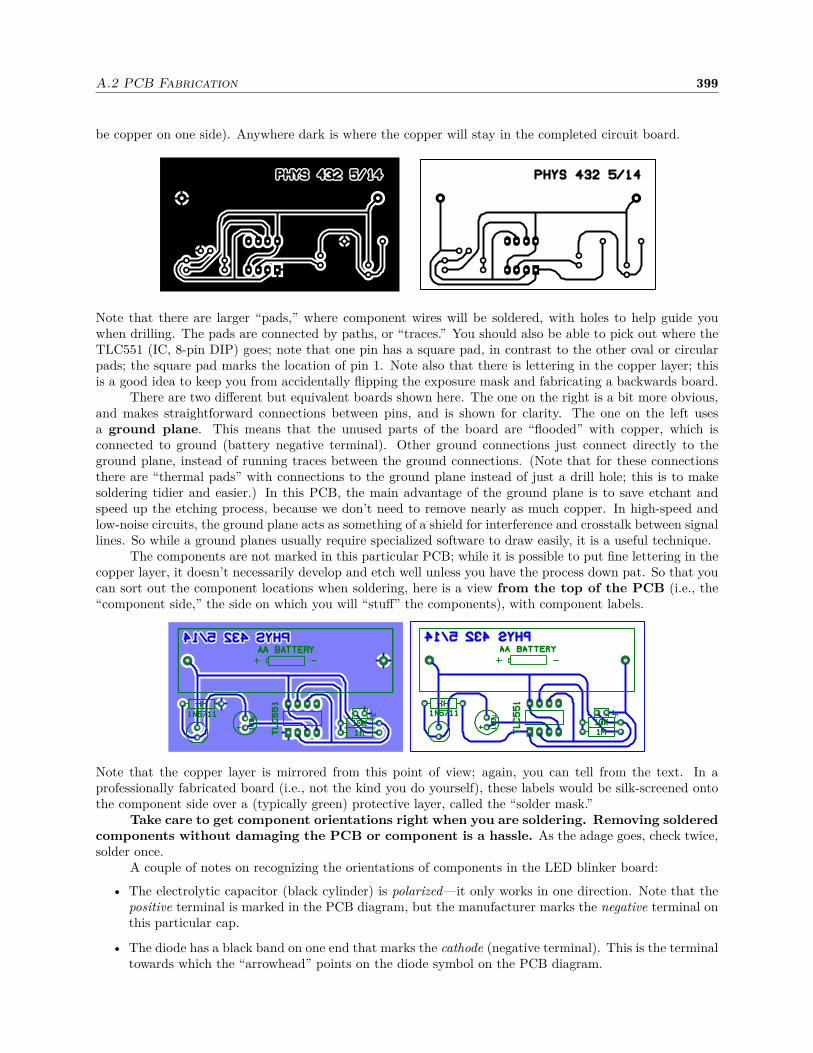
A.2 PCB Fabrication 399
be copper on one side). Anywhere dark is where the copper will stay in the completed circuit board.
Note that there are larger “pads,” where component wires will be soldered, with holes to help guide youwhen drilling. The pads are connected by paths, or “traces.” You should also be able to pick out where theTLC551 (IC, 8-pin DIP) goes; note that one pin has a square pad, in contrast to the other oval or circularpads; the square pad marks the location of pin 1. Note also that there is lettering in the copper layer; thisis a good idea to keep you from accidentally flipping the exposure mask and fabricating a backwards board.
There are two different but equivalent boards shown here. The one on the right is a bit more obvious,and makes straightforward connections between pins, and is shown for clarity. The one on the left usesa ground plane. This means that the unused parts of the board are “flooded” with copper, which isconnected to ground (battery negative terminal). Other ground connections just connect directly to theground plane, instead of running traces between the ground connections. (Note that for these connectionsthere are “thermal pads” with connections to the ground plane instead of just a drill hole; this is to makesoldering tidier and easier.) In this PCB, the main advantage of the ground plane is to save etchant andspeed up the etching process, because we don’t need to remove nearly as much copper. In high-speed andlow-noise circuits, the ground plane acts as something of a shield for interference and crosstalk between signallines. So while a ground planes usually require specialized software to draw easily, it is a useful technique.
The components are not marked in this particular PCB; while it is possible to put fine lettering in thecopper layer, it doesn’t necessarily develop and etch well unless you have the process down pat. So that youcan sort out the component locations when soldering, here is a view from the top of the PCB (i.e., the“component side,” the side on which you will “stuff” the components), with component labels.
Note that the copper layer is mirrored from this point of view; again, you can tell from the text. In aprofessionally fabricated board (i.e., not the kind you do yourself), these labels would be silk-screened ontothe component side over a (typically green) protective layer, called the “solder mask.”
Take care to get component orientations right when you are soldering. Removing solderedcomponents without damaging the PCB or component is a hassle. As the adage goes, check twice,solder once.
A couple of notes on recognizing the orientations of components in the LED blinker board:
• The electrolytic capacitor (black cylinder) is polarized—it only works in one direction. Note that thepositive terminal is marked in the PCB diagram, but the manufacturer marks the negative terminal onthis particular cap.
• The diode has a black band on one end that marks the cathode (negative terminal). This is the terminaltowards which the “arrowhead” points on the diode symbol on the PCB diagram.
400 Appendix A. Homemade Printed Circuit Boards
• The LED cathode is marked by a flat spot on the edge, as shown in the PCB diagram.
• We already discussed pin 1 on the IC. The other components can go in either way, but in general youshould stuff them in the same direction so they are readable (in this board, mostly for the resistors—make the bands “read” from left to right). On the subject of resistors, you should be able to tell theresistors apart by looking at the bands; if you can’t do this, now is a good time to look up how to readresistors!
A.2.2 Presensitized PCBs
Presensitized copper-clad boards come with a layer of photoresist coated onto the copper. The photoresistis sufficient to inhibit etching. With a positive photoresist, you make an optical mask that is opaque whereyou want the copper to stay and transparent where you want the copper to etch away. Then you place themask over the presensitized surface, and expose the masked board to UV light. Then you can chemically“develop” the board, such that the resist is removed wherever it was exposed, and you can proceed to etchaway the copper. There are also boards with negative photoresists (i.e., you expose the parts you want tokeep), but positive boards are simple, cheap, and easily available.
Some sources of positive, presensitized boards that work well are:
• Ever-Muse boards, available from Circuit Specialists.3
• MG Chemicals boards, available from Circuit Specialists or Mouser Electronics.4
These boards are available either single- or double-sided, and in various sizes. The relative prices of the twobrands change often; it’s fine to buy whichever is cheaper at the moment.
A.2.3 Cutting to Size
In general, the presensitized board won’t be the same size as your desired finished circuit. Obviously, youshould start out with a larger board than you need, and then cut it down. If you are only using a small partof a presensitized board, then now is the time to cut it, so you can save the rest of the board to use later.If you only need to cut down the dimensions a bit, or you are fabricating multiple copies of the same board,you can defer cutting until after the board is developed and etched.
One problem with cutting a board with something like a band saw is that the fiberglass is very abrasiveand hard on the saw blade. This also generates fiberglass dust, which is harmful to breathe long-term. Ifyou go this route, make sure to wear a dust mask and protect your lungs.
A more convenient solution is to get your hands on a very old, heavy-duty paper cutter (the greenkind with a large, hinged blade; find these at garage sales or flea markets for cheap). This kind of cuttergoes right through PCBs without generating significant dust. Newer ones may work, but you really need asturdy, hinged blade. Don’t go slicing off your fingertip—be careful.
Note that whichever method you use, you should leave the protective plastic layer on the board whilecutting, in order to protect the delicate photosensitive coating beneath. No matter how careful you are,the photosensitive coating will likely be damaged near the cut edge. This may require some repair beforeetching, or better yet cut the board a bit oversize, so the damaged area is away from any critical areas ofyour PCB layout. Oversize-cutting is a good idea anyway to make sure any critical traces on the PCB arewell away from any edge.
A.2.4 Exposure
In the exposure process, you subject certain areas of the photosensitive layer to UV light. That means youwant to be careful not to subject the layer to any inadvertent UV light. That means, wait to peel off theprotective plastic until right before you are ready to expose, and only handle the exposed board under fairlydim, incandescent lighting (no white-LED or fluorescent lighting).
3http://www.circuitspecialists.com4http://www.mouser.com
A.2 PCB Fabrication 401
You will need a positive exposure mask, which shows your “artwork” (PCB design). Typically,this is a transparency printed via a laser printer, and is dark wherever you want the copper to stay. Forgood results, it is often necessary to “stack” two transparencies to make sure the black-printed areas aredark enough. Align the two transparencies together and use some double-sided tape to hold them togetherin proper alignment.
Now peel off the protective plastic layer of the PCB, starting at one corner and slowly peeling it bypulling the corner towards the opposite corner. You should see a green, shiny layer—the photosensitive layer.Don’t touch the green layer; it’s delicate. Lay the board, green side up, on the table where you will dothe exposure. Lay the exposure mask on top of the board, and align it appropriately (e.g., you may want toput the edges of the mask against the cleanest edges of the board).
The mask must stay flat and pressed against the board during the entire exposure. A sheet of plexiglassor window glass works fine for this. Place the glass on top of the mask, and double-check the mask alignment.
Now you’re ready to expose. This can be done with a specialized UV light, but a simple desktopfluorescent light works well. The board instructions suggest 10–15 W of fluorescent light, 5± 1 cm from theboard, for 8–10 minutes (to compensate for a larger light–board distance, triple the exposure time for everydoubling of the distance). The optimal time depends somewhat on the cover glass and the quality of thetransparency mask, but in practice this recommendation is excessively long. A good example choice for alamp we will use employs a 15-W fluorescent bulb, held about 13 cm above the table top. For this setup, an8-minute exposure is appropriate, using an object to get the board within about 2” from the light.
Underexposure is bad, as not all of the photosensitive layer will be removed from the board. Smallgaps in the copper may not develop properly.
Overexposure is also bad, as the copper traces will come out too thin, and may be broken in someareas. Of course, if extremely overdeveloped, there won’t be any photoresist left at all. This process is notespecially sensitive to the exposure time, but it’s important to get it within a reasonable range.
If you are doing a double-sided board, you should now proceed with exposing the other side of theboard. These are a bit tricky, as it is hard to keep the artwork for the two sides in alignment with respect tothe board. If they’re not well-aligned, you’ll see exactly what the problems are when you start drilling theboard. The trick here is to tape the front and back layers together in proper alignment right at the beginning
(e.g., with double-sided tape). Then slide the board in between the two masks (with protective plastics onboth sides removed), and proceed with exposure. The only hard part is making sure the board doesn’t movewith respect to the masks when you flip it over to do the other side.
After exposure, if you look at the board under bright (incandescent) light, you may see that the exposedareas have changed to a slightly different shade of green, and you can see a faint “imprint” of the artwork.Don’t waste time now; you should proceed to developing your board immediately.
A.2.5 Developing
The board is developed in a room-temperature bath of NaOH solution. The bath is not especially caustic,but you should still don a nitrile glove.
Developer solution is available from MG Chemicals (via Mouser or Circuit Specialists), which youdilute according to the instructions. However, this is a simple NaOH solution, at 1% concentration byweight (i.e., mixed into tap water, 10 g NaOH per L of solution). For safety, add the NaOH to the fullamount of water to avoid inadvertently dealing with a concentrated, caustic solution. This solution must bethoroughly mixed before use, otherwise you might get uneven results when you develop your board. Afterdeveloping a board, this solution seems to go flat after a few months (probably due to air exposure). In anycase, don’t use old developer unless you know it to be fresh enough; it’s better to make up a new batch forreliability.
The developer is easiest to handle in a wide, polyethylene or polypropylene container (e.g., a widetupperware-type food-grade container, labeled for non-food use!). NaOH reacts with some metals, so metalcontainers are out, and glass containers are okay but susceptible to breakage.
Using your gloved hand, dip the board into the developer bath, and gently move it around to keepfresh developer in contact with the board. You should see photoresist beginning to “smoke” off the boardimmediately, and the exposed areas should develop to shiny copper in less than a couple of minutes. Keep
402 Appendix A. Homemade Printed Circuit Boards
developing for 30 seconds after it looks like it’s done, otherwise there may be a very thin layer of photoresiston some of the shiny areas that will inhibit etching. Then rinse off the board. Be careful not to dripdeveloper all over the place.
Carefully inspect the board. Are there areas that didn’t develop properly? You may need to “edit”the photoresist layer by carefully scraping bits away using an X-acto knife. Are there areas that haveoverdeveloped, flaked away, or are there defects (pinholes, etc.) in any of the traces? You can “repair”photoresist by using a permanent Sharpie marker to make small edits. Also, before proceeding to theetching step, if there are large swaths of exposed copper, say near an edge of the board that you don’t careabout (e.g., because you started off with an oversized board), you should mask off that part of the board(with masking tape) so you don’t waste etching solution on things that don’t need to be etched.
A.2.6 Etching
For etching the copper, there are two commonly used chemicals. The first is ferric chloride. We will avoidthis, because it is pretty nasty stuff that looks like toxic sludge, and it will stain your skin and clothing.Otherwise, it works just fine. You can usually buy it as a concentrated solution or as a powder. Both requiremixing with water. Be careful with power in the anhydrous form, as it is very exothermic while dissolvingin water—start with the full amount of cold water and add the powder slowly and carefully to the water.Again, a polyethylene container is best for etching and storage, and glass can be used for longer-term storage.
The etchant we will use is ammonium persulfate, available from MG Chemicals (P/N 410-1KG,via the usual suspects), in 1 kg bottles of dry crystals. (Sodium persulfate is another, similar alternativeetchant.) This is mixed in a ratio of 250 g of crystals into 1 L of tap water, and interestingly is endothermicwhen you mix it. This chemical has the advantage of being somewhat less nasty than ferric chloride, andit’s transparent, so you can see the board while it’s etching. (It also works less well than ferric chloridein terms of the Sharpie trick.) However, you have to be careful with it. Never store the etchant in ametal container. Never use a tightly sealed container (glass or otherwise) for the etchant forlong-term storage. Disobey these and you risk an explosion—not fun. A tall polyethylene container isgood for etching, because it’s inert and shatter-resistant, and taller containers meant for cereal are goodbecause they have tops that will pop open in case of pressure build-up.
And it should go without saying: Don’t dump these chemicals down the drain. Disposeof them properly.5 In particular, ammonium persulfate should not be mixed with acids, alcohols, orflammables (or anything else, just in case) for disposal. Also, in case of spilled etchant, wipe it up with wetpaper towels (and make sure they stay wet)—etchants are oxidizers, which can pose a fire hazard.
Any etchant works faster at an elevated temperature (40C is plenty), but room temperature is fine ifyou’re patient. Agitation is also essential to a good etch; this can include periodically change the orientationof the board and moving the board around, stirring the bath with a stir plate, or bubbling air through thebath with an aquarium pump.
Make sure to wear nitrile gloves when handling etchant or boards going into the etchant. Dip theboard into the etchant with your gloved hand, until the shiny copper areas turn dark and reddish. Pull theboard out and look for any remaining shiny copper spots. These are areas where there is still a thin layerof photoresist, and you must fix these. After rinsing the board in water, you can scrape these areas witha knife. Alternately, you may have success with rubbing the area with a dry paper towel—if you do thiscarefully, this will abrade the thin layer without damaging the thicker areas that are supposed to stay.
When the board is etching correctly, place it in the etchant tank in a way that makes it convenient toretrieve with a gloved hand. You could hang it using some fishing line, or in the lab we have a plastic “rack”for boards with a handle that makes it easy to retrieve. Gently agitate the etchant once in a while—this willspeed up the etching, which will take some time (10–30 minutes).
5In Lane County, Oregon, for example, household hazardous waste is accepted (at no charge) at Glenwood Central ReceivingStation: http://www.lanecounty.org/departments/pw/wmd/hazwaste/pages/hhwcc.aspx. On UO campus, hazardous waste iscollected by Environmental Health & Safety: http://ehs.uoregon.edu.
A.2 PCB Fabrication 403
A.2.7 Drilling
Before proceeding with drilling, check to see if your board has any sharp copper edges that might cut you.If so, sand them off as described in the next section.
Drilling a PCB is best accomplished with a small drill press. A reasonably good yet economical choiceis a drill-press mount for a Dremel tool.
Another good, economical choice for drilling in this setup comes in the form of miniature, high-speed-steel drill bits, available for cheap from Harbor Freight. The typical hole size for small components is 0.8 mm(larger for high-power or large components), but a somewhat larger drill bit can be used to reduce drillbreakage. On the example PCB you are drilling, you need a larger drill bit (a mm or a bit over) for thebattery-mount holes. These bits fit directly into the collet of the Dremel tool (i.e., no drill chuck is necessary).
Some safety/operation notes:
• Small drill bits (especially carbide bits, but steel bits too) are brittle, and lead to small bits of sharp,flying shrapnel when they break. Always wear eye protection when drilling PCBs. Flyingshrapnel piercing cornea = BAD.
• Avoid breaking drill bits in the first place. When drilling, use gentle pressure on the bit. If younotice any flex in the bit, STOP and figure out what’s wrong.
• The main cause of bit breakage is movement of the PCB while drilling. Hold the PCB firmly againstthe base of the drill press to avoid (1) general side-to-side movement and (2) upward movement whenthe bit snags on the way out the bottom side. In general, keeping the piece in place is good drillingtechnique; while this is unlikely with small bits, a snagged drill bit can result in a dangerous spinningobject if you don’t have it firmly planted.
• Run the Dremel tool at the low end of its speed range.
• After you finish, rinse off the PCB to get rid of dust. (Drilling doesn’t generate a whole lot of dust,but it’s best not to blow it into the air.)
• Double-check that every hole is drilled; if you discover an undrilled hole after you have half the boardstuffed, it’s awkward (to say the least!) to go back and fix it. Work in a pattern (e.g., left-to-right,then front-to-back) to reduce your chances of missing a hole.
A.2.8 Cleaning Up the Board Dimensions
Now is the time to get the outer dimensions of the board down to size. If you have large areas to trim off,go ahead and do this with a cutter, as described above. To trim down a side by a couple of mm or so, usesandpaper. Wet the sandpaper to eliminate airborne dust (use “wet/dry” sandpaper designed for this). Laythe sandpaper on a flat surface and rub the PCB against it, in the direction of the PCB, until the dimensionand surface quality are up to your standards.
Non-rectangular board outlines are also possible, but require other tools such as routers or copingsaws—with appropriate dust control, of course.
A.2.9 Preparing to Solder
Now is the time to remove the green photoresist layer from the PCB. This is easy to do by rinsing off theboard with acetone or methanol. Be careful not to get solvent on the table or other things, as they candamage a wide variety of materials. Use a glove to protect your hand from solvent and photoresist.
At this point the exposed copper should be bright and shiny. If not, rub it with steel wool to removeany oxides. Make sure not to touch the board with bare skin, as your skin oils will oxidize and etch thesurface.
404 Appendix A. Homemade Printed Circuit Boards
A.2.10 Soldering
Soldering is a delicate balance between too little and too much heat. Too little, and the solder won’t stickto the PCB and component you’re trying to connect (in the worst case, you can get a cold-solder joint,which looks like a good solder joint, but forms a poor and/or intermittent connect—very hard to debug.Too much heat, and you can fry delicate components, or cause the copper foil to delaminate from the PCB(difficult to fix).
The key to successful soldering is to be fast—heat things up, make the joint, and then let it cool down.This way you can solder at an appropriately high temperature, and cool the joint down before heat travelsenough to damage any components. Here are the details, step-by-step.
• You’ll need a soldering iron. Most things will work, from a $10 soldering pen to a regulated solderingstation (the kind with a temperature control on the base). Let the iron heat up for a few minutes untilit equilibrates. Solder should melt immediately when you touch it to the iron.
• You also need solder, obviously. Lead-based solder is far easier to work with than lead-free. You shouldalso use rosin-core solder (never use acid-core solder on electronics). This solder contains rosin-basedflux, which chemically removes oxides from metal to be soldered when heated. It helps the solder“wet” the bare copper and the component lead.
• To mount a component, begin by inserting it into the PCB, double-checking its position and orientation,as de-soldering components is a pain. For things with long leads like resistors and capacitors, you canbend the leads a bit (no more than 30—less is better, in case you ever need to replace the component).For things like ICs with short leads, they will ideally stick in place if you’ve used appropriately sizedholes. If not, you can use some masking tape to hold them in place while you solder. A quicker solutionwhen you are more experienced is to use one hand to hold the board, with one finger holding the ICin place. Then quickly solder pins on opposite corners with your other hand, by touching the solderwith the iron and quickly transferring it to the solder joints. This is bad soldering technique (the jointswon’t be properly fluxed, and you can’t use very much heat if you don’t want to burn your finger),but you can use these temporary joints to hold the IC while you solder the rest of the pins with bothhands. Then come back and redo the temporary joints.
• To make a solder joint, begin by touching the iron to both the pin and the pad that you’re joining. Laythe soldering iron down for the largest possible contact area—the key is heating things up quickly. Infact, for this reason, large flat soldering-iron tips are preferable to needle-shaped tips, even for fairlyfine solder work. The metal should be hot within a second or two. Now to bring in the solder; youcan work with a small piece, or hold the whole roll in your hand for stability. Touch the end of thesolder wire to the iron tip. As soon as it begins to melt, move the end of the solder wire from thetip to the joint itself, and start feeding the wire into the joint. (That is, you should be feeding intothe intersection between the component and copper foil, not into the soldering-iron tip.) If the wiredoesn’t feed because it’s not melting, it means you don’t have enough heat at the junction. Feed thesolder until you have enough solder to make a conical blob, pointing along the component wire. Assoon as you have enough solder, remove the wire and iron, and blow on the joint to cool it off quickly,to avoid overheating anything. Incidentally, it’s good to inhale before touching the solder to the iron,and exhale after the joint is done, so you don’t breathe the rosin smoke.
• Check your joint: It shouldn’t bulge like a sphere, but it should be enough solder to “fill out” thejunction. The solder should be nice and shiny. If not, heat it back up and try to correct it; you canuse the iron tip to “wipe away” excess solder (you can then use a wet sponge or paper towel to cleanexcess solder from the iron), and then add fresh solder to make a good joint.
A.2.11 Stuffing in Stages
When stuffing (inserting components and soldering) a PCB, there are some good rules to follow to save youfrom later headaches.
A.3 Characterizing the Circuit 405
• It’s easiest to stuff small components (resistors, ICs) first, and then larger components (large capacitors,inductors) later—once the big boys are in place, it’s harder to maneuver.
• Even more importantly, you should build the board in logical stages, starting with the any power-supply section, and then test each section as you go. It’s much easier to debug a circuit if you’veonly stuffed a small part of it, compared to dealing with a whole populated board. Go down thesignal chain, stuffing and testing. In the example circuit here, you would start with the battery mount(violating the first rule here), then the IC and resistors and timing capacitor, then see that the circuitis oscillating as expected, and only then add the diode, LED, and boosting capacitor.
A.2.12 Protection
To save time, we will skip this step in lab, but this is something you can do later if you like. To protect thecopper traces from oxidizing, they need a protective coating. In professionally fabricated boards, the copperis plated in nickel before soldering, and this works well. There are chemical kits that allow you to chemicallyplate your own PCBs, but their performance is variable, and it’s usually not worth the expense and hassle.
The alternative is to coat the board after soldering with “conformal coating,” available in severalmaterials. Acrylic conformal coating works well. It’s something like a spray paint, but goes on thick enoughto flow around components and solder joints, and dries to a clear layer. For repairs, a soldering iron willburn right through it. Note that this layer also insulates, so it must be scraped off for measuring voltageswith probes. Also before spraying, make sure to mask off any components that shouldn’t get gummed upwith the coating material (jacks and connectors, pots, trim pots, edge connectors, etc.).
Before you spray on the coating, you must remove the flux from the soldering step, otherwise theconformal coating will look bad or may not adhere well. You can do this by giving the board a bath inisopropanol (ordinary rubbing alcohol; don’t use stronger solvents like acetone, which will eat components).You will also need to use a stiff brush (toothbrush or camel-hair brush) to clean off the most stubborn bitsof flux, or use an ultrasonic bath if you have one.
Another trick is to brush on a layer of liquid rosin flux6 before soldering, and let it dry. It will be kindof sticky for a day or more until it dries thoroughly but after that it makes a nice, hard, solderable layerthat resists oxidation. It can be cleaned off using isopropanol to put on a conformal coating later.
A.3 Characterizing the Circuit
Now that you have the circuit stuffed, put in the battery. You should see the LED flashing. If not, recheckthe circuit.
Make sure you understand the circuit:
1. Does the period of the blinking match your expectation from the resistor and capacitor values?
2. Make a timing diagram for the circuit (using an oscilloscope to measure the voltages) at pins 2 and3 of the TLC551 (comparator input and oscillator output), as well as the LED cathode (reference allyour voltages to “ground,” the negative terminal of the battery).
3. Based on your timing diagram, explain: how does the circuit light a 1.8 V LED using a 1.5 V battery?
6e.g., M.G. Chemicals 835: http://www.mgchemicals.com/products/solder/fluxes/rosin-flux-835/

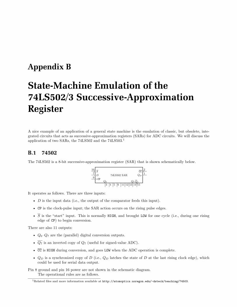
Appendix B
State-Machine Emulation of the74LS502/3 Successive-ApproximationRegister
A nice example of an application of a general state machine is the emulation of classic, but obsolete, inte-grated circuits that acts as successive-approximation registers (SARs) for ADC circuits. We will discuss theapplication of two SARs, the 74LS502 and the 74LS503.1
B.1 74502
The 74LS502 is a 8-bit successive-approximation register (SAR) that is shown schematically below.
74LS502 SAR
>CP9
S10
7D
CC2
QD1
3 4 5 6 11 12 13 14Q0 Q7
15Q7
It operates as follows. There are three inputs:
• D is the input data (i.e., the output of the comparator feeds this input).
• CP is the clock-pulse input; the SAR action occurs on the rising pulse edges.
• S is the “start” input. This is normally HIGH, and brought LOW for one cycle (i.e., during one risingedge of CP) to begin conversion.
There are also 11 outputs:
• Q0–Q7 are the (parallel) digital conversion outputs.
• Q7 is an inverted copy of Q7 (useful for signed-value ADC).
• CC is HIGH during conversion, and goes LOW when the ADC operation is complete.
• QD is a synchronized copy of D (i.e., QD latches the state of D at the last rising clock edge), whichcould be used for serial data output.
Pin 8 ground and pin 16 power are not shown in the schematic diagram.The operational rules are as follows.
1Related files and more information available at http://atomoptics.uoregon.edu/~dsteck/teaching/74503.
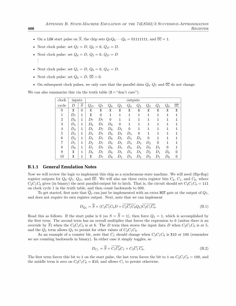
408Appendix B. State-Machine Emulation of the 74LS502/3 Successive-Approximation
Register
• On a LOW start pulse on S, the chip sets Q7Q6 · · ·Q0 = 01111111, and CC = 1.
• Next clock pulse: set Q7 = D, Q6 = 0, QD = D.
• Next clock pulse: set Q6 = D, Q5 = 0, QD = D...
• Next clock pulse: set Q1 = D, Q0 = 0, QD = D.
• Next clock pulse: set Q0 = D, CC = 0.
• On subsequent clock pulses, we only care that the parallel data Q0–Q7 and CC do not change.
We can also summarize this via the truth table (X = “don’t care”):
clock inputs outputs
cycle D S QD Q7 Q6 Q5 Q4 Q3 Q2 Q1 Q0 CC
0 X 0 X X X X X X X X X X
1 D7 1 X 0 1 1 1 1 1 1 1 1
2 D6 1 D7 D7 0 1 1 1 1 1 1 1
3 D5 1 D6 D7 D6 0 1 1 1 1 1 1
4 D4 1 D5 D7 D6 D5 0 1 1 1 1 1
5 D3 1 D4 D7 D6 D5 D4 0 1 1 1 1
6 D2 1 D3 D7 D6 D5 D4 D3 0 1 1 1
7 D1 1 D2 D7 D6 D5 D4 D3 D2 0 1 1
8 D0 1 D1 D7 D6 D5 D4 D3 D2 D1 0 1
9 X 1 D0 D7 D6 D5 D4 D3 D2 D1 D0 0
10 X 1 X D7 D6 D5 D4 D3 D2 D1 D0 0
B.1.1 General Emulation Notes
Now we will review the logic to implement this chip as a synchronous state machine. We will need (flip-flop)register outputs for Q0–Q7, QD, and CC. We will also use three extra register bits C2, C1, and C0, whereC2C1C0 gives (in binary) the next parallel-output bit to latch. That is, the circuit should set C2C1C0 = 111
on clock cycle 1 in the truth table, and then count backwards to 000.To get started, first note that Q7 can just be implemented with an extra NOT gate at the output of Q7,
and does not require its own register output. Next, note that we can implement
DQ5= S + (C2C1C0D + C2C1C0Q5)C2C1C0. (B.1)
Read this as follows. If the start pulse is 0 (so S = S = 1), then force Q5 = 1, which is accomplished bythe first term. The second term has an overall multiplier that forces the expression to 0 (unless there is anoverride by S) when the C2C1C0 is at 6. The D term then stores the input data D when C2C1C0 is at 5,and the Q5 term allows Q5 to persist for other values of C2C1C0.
As an example of a counter bit, note that C1 should change when C2C1C0 is X10 or 100 (rememberwe are counting backwards in binary). In either case it simply toggles, so
DC1= S + C1C0C1 + C2C1 C0. (B.2)
The first term forces this bit to 1 on the start pulse, the last term forces the bit to 1 on C2C1C0 = 100, andthe middle term is zero on C2C1C0 = X10, and allows C1 to persist otherwise.

B.1 74502 409
The complete set of logic expressions is as follows.
DQ7= S(C2C1C0D + C2C1C0Q7)
DQ6= S + (C2C1C0D + C2C1C0Q6)C2C1C0
DQ5= S + (C2C1C0D + C2C1C0Q5)C2C1C0
DQ4= S + (C2C1 C0D + C2C1 C0Q4)C2C1C0
DQ3= S + (C2C1C0D + C2C1C0Q3)C2C1 C0
DQ2= S + (C2C1C0D + C2C1C0Q2)C2C1C0
DQ1= S + (C2 C1C0D + C2 C1C0Q1)C2C1C0
DQ0= S + (C2 C1 C0 CCD + C2 C1 C0 CCQ0)C2 C1C0
DCC = S + C2 C1 C0 CC
DC2= S + C2C1 C0 C2
DC1= S + C1C0C1 + C2C1 C0
DC0= S + C2 C1 C0 C0
DQD= D
Q7 = (Q7)
(B.3)
To understand all these in some detail:
• The easiest ones to understand are the last two: Q7 is just an inverted copy of Q7, and QD just latchesD.
• On all the others, the start pulse forces the bits to 1, except for Q7, which is forced to 0. Note thatthe start pulse overrides all other information.
• Then Q7 loads D when C2C1C0 = 111 and persists otherwise. We covered the similar logic for Q5
already; Q0–Q4 and Q6 follow the same idea in persisting, except changing to 0 and storing D at theright stages. However, Q0 is slightly more complicated since we stop the counter on C2C1C0 = 000,so we must also use the CC bit to make sure the state of Q0 persists when conversion is complete.
• For CC, this should be forced to zero on C2C1C0 = 000 (i.e., after the last comparison), otherwise itpersists. The factor of CC is not strictly necessary on the second term.
• We covered the logic of the C1 counter bit already. Then C0 is simple in toggling on each clock pulse,except that once C2C1C0 = 000, we will force it to stay at 0. For C2, the MSB should only change onC2C1C0 = 100, so we detect this case explicitly and use a NOT operation to reset to 0, otherwise C2
persists.
B.1.2 22V10 Emulation
To emulate the 74LS502, we will choose the 22V10 SPLD (e.g., the ATF22V10C from Atmel). This has a10-bit register (i.e., 10 D-type flip-flops) and 10 outputs, plus plenty of logic for sum-of-product logic andplenty of inputs. However, there is a problem: we have 13 registered outputs, but only 10 bits in the register.To handle this, note that the counter-logic bits C0–C2 are actually redundant–and-that is, although they areconceptually useful states in writing down the state-machine logic, they are not needed as register variablesin the sense that they can be inferred from the other register variables Q0–Q7 and CC. In particular, notethat
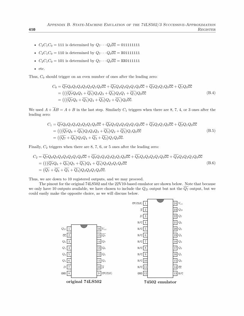
410Appendix B. State-Machine Emulation of the 74LS502/3 Successive-Approximation
Register
• C2C1C0 = 111 is determined by Q7 · · ·Q0CC = 011111111
• C2C1C0 = 110 is determined by Q7 · · ·Q0CC = X01111111
• C2C1C0 = 101 is determined by Q7 · · ·Q0CC = XX0111111
• etc.
Thus, C0 should trigger on an even number of ones after the leading zero:
C0 = Q7Q6Q5Q4Q3Q2Q1Q0CC + Q5Q4Q3Q2Q1Q0CC + Q3Q2Q1Q0CC + Q1Q0CC
=(((
Q7Q6Q5 + Q5
)
Q4Q3 + Q3
)
Q2Q1 + Q1
)
Q0CC
=(((
Q7Q6 + Q5
)
Q4 + Q3
)
Q2 + Q1
)
Q0CC.
(B.4)
We used A + AB = A + B in the last step. Similarly C1 triggers when there are 8, 7, 4, or 3 ones after theleading zero:
C1 = Q7Q6Q5Q4Q3Q2Q1Q0CC + Q6Q5Q4Q3Q2Q1Q0CC + Q3Q2Q1Q0CC + Q2Q1Q0CC
=(((
Q7Q6 + Q6
)
Q5Q4Q3 + Q3
)
Q2 + Q2
)
Q1Q0CC
=((
Q7 + Q6
)
Q5Q4 + Q3 + Q2
)
Q1Q0CC.
(B.5)
Finally, C2 triggers when there are 8, 7, 6, or 5 ones after the leading zero:
C2 = Q7Q6Q5Q4Q3Q2Q1Q0CC + Q6Q5Q4Q3Q2Q1Q0CC + Q5Q4Q3Q2Q1Q0CC + Q4Q3Q2Q1Q0CC
=(((
Q7Q6 + Q6
)
Q5 + Q5
)
Q4 + Q4
)
Q3Q2Q1Q0CC
=(
Q7 + Q6 + Q5 + Q4
)
Q3Q2Q1Q0CC.
(B.6)
Thus, we are down to 10 registered outputs, and we may proceed.The pinout for the original 74LS502 and the 22V10-based emulator are shown below. Note that because
we only have 10 outputs available, we have chosen to include the QD output but not the Q7 output, but wecould easily make the opposite choice, as we will discuss below.
12
11
10
9
8
7
6
5
4
3
2
1
13
14
15
16
17
18
19
20
21
22
23
24
GND
N/C
N/C
N/C
N/C
N/C
N/C
N/C
N/C
D
S
CP(CLK)
N/C
CC
Q0
Q1
Q2
Q3
Q4
Q5
Q6
Q7
QD
VCC
74502 emulator
8
7
6
5
4
3
2
1
9
10
11
12
13
14
15
16
GND
D
Q3
Q2
Q1
Q0
CC
QD
CP(CLK)
S
Q4
Q5
Q6
Q7
Q7
VCC
original 74LS502

B.1 74502 411
The code to implement the state machine in the CUPL (Compiler for Universal Programmable Logic)programming language2 is shown below.
74502-22V10.pld
/*
* 74502 SAR emulator, on a 22v10
*/
Name 74502-22V10;
Partno 74502;
Revision 01;
Date 5/23/2015;
Designer Daniel Steck;
Company University of Oregon;
Location None;
Assembly None;
Device g22v10;
/*** inputs ***/
pin 1 = CP; /* clock pulse (trig on rising edge) */
pin 2 = !S; /* start low */
pin 3 = Din; /* data */
/*** outputs ***/
pin 14 = !CC; /* conversion complete low */
pin [15..22] = [Q0..Q7]; /* 8-bit output */
pin 23 = QD; /* registered/synchronous copy of data input */
/*** intermediate counter variables ***/
C0 = (((!Q7 & Q6 # !Q5) & Q4 # !Q3) & Q2 # !Q1) & Q0 & !CC;
C1 = ((!Q7 # !Q6) & Q5 & Q4 # !Q3 # !Q2) & Q1 & Q0 & !CC;
C2 = (!Q7 # !Q6 # !Q5 # !Q4) & Q3 & Q2 & Q1 & Q0 & !CC;
/*** register inputs ***/
CC.D = !(S # !(!C2 & !C1 & !C0) & !CC);
Q7.D = !S & (C2 & C1 & C0 & Din # !(C2 & C1 & C0) & Q7);
Q6.D = S # ( C2 & C1 & !C0 & Din # !( C2 & C1 & !C0) & Q6) & !( C2 & C1 & C0);
Q5.D = S # ( C2 & !C1 & C0 & Din # !( C2 & !C1 & C0) & Q5) & !( C2 & C1 & !C0);
Q4.D = S # ( C2 & !C1 & !C0 & Din # !( C2 & !C1 & !C0) & Q4) & !( C2 & !C1 & C0);
Q3.D = S # (!C2 & C1 & C0 & Din # !(!C2 & C1 & C0) & Q3) & !( C2 & !C1 & !C0);
Q2.D = S # (!C2 & C1 & !C0 & Din # !(!C2 & C1 & !C0) & Q2) & !(!C2 & C1 & C0);
Q1.D = S # (!C2 & !C1 & C0 & Din # !(!C2 & !C1 & C0) & Q1) & !(!C2 & C1 & !C0);
Q0.D = S # (!C2 & !C1 & !C0 & !CC & Din # !(!C2 & !C1 & !C0 & !CC) & Q0) & !(!C2 & !C1 & C0);
QD.D = Din;
/*** handle flip-flop variables set/preset inputs ***/
CC.ar = 'b'0;
Q7.ar = 'b'0;
Q6.ar = 'b'0;
Q5.ar = 'b'0;
Q4.ar = 'b'0;
Q3.ar = 'b'0;
Q2.ar = 'b'0;
Q1.ar = 'b'0;
Q0.ar = 'b'0;
QD.ar = 'b'0;
2The only compiler realistically available nowadays is WinCUPL, which is Windows-based, crash-prone, and proprietary,but it is freely distributed by Atmel: http://www.atmel.com/tools/wincupl.aspx.
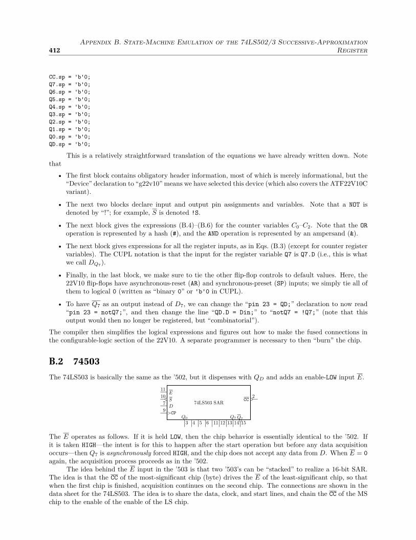
412Appendix B. State-Machine Emulation of the 74LS502/3 Successive-Approximation
Register
CC.sp = 'b'0;
Q7.sp = 'b'0;
Q6.sp = 'b'0;
Q5.sp = 'b'0;
Q4.sp = 'b'0;
Q3.sp = 'b'0;
Q2.sp = 'b'0;
Q1.sp = 'b'0;
Q0.sp = 'b'0;
QD.sp = 'b'0;
This is a relatively straightforward translation of the equations we have already written down. Notethat
• The first block contains obligatory header information, most of which is merely informational, but the“Device” declaration to “g22v10” means we have selected this device (which also covers the ATF22V10Cvariant).
• The next two blocks declare input and output pin assignments and variables. Note that a NOT isdenoted by “!”; for example, S is denoted !S.
• The next block gives the expressions (B.4)–(B.6) for the counter variables C0–C2. Note that the OR
operation is represented by a hash (#), and the AND operation is represented by an ampersand (&).
• The next block gives expressions for all the register inputs, as in Eqs. (B.3) (except for counter registervariables). The CUPL notation is that the input for the register variable Q7 is Q7.D (i.e., this is whatwe call DQ7
).
• Finally, in the last block, we make sure to tie the other flip-flop controls to default values. Here, the22V10 flip-flops have asynchronous-reset (AR) and synchronous-preset (SP) inputs; we simply tie all ofthem to logical 0 (written as “binary 0” or 'b'0 in CUPL).
• To have Q7 as an output instead of D7, we can change the “pin 23 = QD;” declaration to now read“pin 23 = notQ7;”, and then change the line “QD.D = Din;” to “notQ7 = !Q7;” (note that thisoutput would then no longer be registered, but “combinatorial”).
The compiler then simplifies the logical expressions and figures out how to make the fused connections inthe configurable-logic section of the 22V10. A separate programmer is necessary to then “burn” the chip.
B.2 74503
The 74LS503 is basically the same as the ’502, but it dispenses with QD and adds an enable-LOW input E.
74LS503 SAR
>CP9
S10
E11
7D
CC2
3 4 5 6 11 12 13 14Q0 Q7
15Q7
The E operates as follows. If it is held LOW, then the chip behavior is essentially identical to the ’502. Ifit is taken HIGH—the intent is for this to happen after the start operation but before any data acquisitionoccurs—then Q7 is asynchronously forced HIGH, and the chip does not accept any data from D. When E = 0
again, the acquisition process proceeds as in the ’502.The idea behind the E input in the ’503 is that two ’503’s can be “stacked” to realize a 16-bit SAR.
The idea is that the CC of the most-significant chip (byte) drives the E of the least-significant chip, so thatwhen the first chip is finished, acquisition continues on the second chip. The connections are shown in thedata sheet for the 74LS503. The idea is to share the data, clock, and start lines, and chain the CC of the MSchip to the enable of the enable of the LS chip.
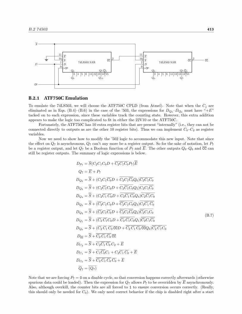
B.2 74503 413
74LS503 SAR
>CP9
S10
E11
7D
CC2
3 4 5 6 11 12 13 14Q0 Q7
15Q7
74LS503 SAR
>CP9
S10
E11
7D
CC2
3 4 5 6 11 12 13 14Q0 Q7
15Q7
S
D
CP
CC
Q8 Q15 Q0 Q7
B.2.1 ATF750C Emulation
To emulate the 74LS503, we will choose the ATF750C CPLD (from Atmel). Note that when the Cj areeliminated as in Eqs. (B.4)–(B.6) in the case of the ’503, the expressions for DQ0
–DQ6must have “+E”
tacked on to each expression, since these variables track the counting state. However, this extra additionappears to make the logic too complicated to fit in either the 22V10 or the ATF750C.
Fortunately, the ATF750C has 10 extra register bits that are present “internally” (i.e., they can not beconnected directly to outputs as are the other 10 register bits). Thus we can implement C0–C2 as registervariables.
Now we need to show how to modify the ’502 logic to accommodate this new input. Note that sincethe effect on Q7 is asynchronous, Q7 can’t any more be a register output. So for the sake of notation, let P7
be a register output, and let Q7 be a Boolean function of P7 and E. The other outputs Q0–Q6 and CC canstill be register outputs. The summary of logic expressions is below.
DP7= S(C2C1C0D + C2C1C0P7)E
Q7 = E + P7
DQ6= S + (C2C1C0D + C2C1C0Q6)C2C1C0
DQ5= S + (C2C1C0D + C2C1C0Q5)C2C1C0
DQ4= S + (C2C1 C0D + C2C1 C0Q4)C2C1C0
DQ3= S + (C2C1C0D + C2C1C0Q3)C2C1 C0
DQ2= S + (C2C1C0D + C2C1C0Q2)C2C1C0
DQ1= S + (C2 C1C0D + C2 C1C0Q1)C2C1C0
DQ0= S + (C2 C1 C0 CCD + C2 C1 C0 CCQ0)C2 C1C0
DCC = S + C2 C1 C0 CC
DC2= S + C2C1 C0 C2 + E
DC1= S + C1C0C1 + C2C1 C0 + E
DC0= S + C2 C1 C0 C0 + E
Q7 = (Q7)
(B.7)
Note that we are forcing P7 = 0 on a disable cycle, so that conversion happens correctly afterwards (otherwisespurious data could be loaded). Then the expression for Q7 allows P7 to be overridden by E asynchronously.Also, although overkill, the counter bits are all forced to 1 to ensure conversion occurs correctly. (Really,this should only be needed for C0). We only need correct behavior if the chip is disabled right after a start
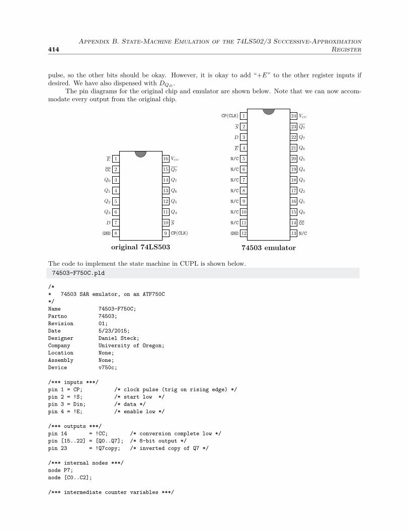
414Appendix B. State-Machine Emulation of the 74LS502/3 Successive-Approximation
Register
pulse, so the other bits should be okay. However, it is okay to add “+E” to the other register inputs ifdesired. We have also dispensed with DQD
.The pin diagrams for the original chip and emulator are shown below. Note that we can now accom-
modate every output from the original chip.
12
11
10
9
8
7
6
5
4
3
2
1
13
14
15
16
17
18
19
20
21
22
23
24
GND
N/C
N/C
N/C
N/C
N/C
N/C
N/C
E
D
S
CP(CLK)
N/C
CC
Q0
Q1
Q2
Q3
Q4
Q5
Q6
Q7
Q7
VCC
74503 emulator
8
7
6
5
4
3
2
1
9
10
11
12
13
14
15
16
GND
D
Q3
Q2
Q1
Q0
CC
E
CP(CLK)
S
Q4
Q5
Q6
Q7
Q7
VCC
original 74LS503
The code to implement the state machine in CUPL is shown below.
74503-F750C.pld
/*
* 74503 SAR emulator, on an ATF750C
*/
Name 74503-F750C;
Partno 74503;
Revision 01;
Date 5/23/2015;
Designer Daniel Steck;
Company University of Oregon;
Location None;
Assembly None;
Device v750c;
/*** inputs ***/
pin 1 = CP; /* clock pulse (trig on rising edge) */
pin 2 = !S; /* start low */
pin 3 = Din; /* data */
pin 4 = !E; /* enable low */
/*** outputs ***/
pin 14 = !CC; /* conversion complete low */
pin [15..22] = [Q0..Q7]; /* 8-bit output */
pin 23 = !Q7copy; /* inverted copy of Q7 */
/*** internal nodes ***/
node P7;
node [C0..C2];
/*** intermediate counter variables ***/

B.2 74503 415
C0.D = S # !(!C2 & !C1 & !C0) & !C0 # !E;
C1.D = S # !(C1 & !C0) & C1 # C2 & !C1 & !C0 # !E;
C2.D = S # !(C2 & !C1 & !C0) & C2 # !E;
/*** register inputs ***/
CC.D = !(S # !(!C2 & !C1 & !C0) & !CC);
P7.D = !S & (C2 & C1 & C0 & Din # !(C2 & C1 & C0) & P7) & E;
Q6.D = S # ( C2 & C1 & !C0 & Din # !( C2 & C1 & !C0) & Q6) & !( C2 & C1 & C0);
Q5.D = S # ( C2 & !C1 & C0 & Din # !( C2 & !C1 & C0) & Q5) & !( C2 & C1 & !C0);
Q4.D = S # ( C2 & !C1 & !C0 & Din # !( C2 & !C1 & !C0) & Q4) & !( C2 & !C1 & C0);
Q3.D = S # (!C2 & C1 & C0 & Din # !(!C2 & C1 & C0) & Q3) & !( C2 & !C1 & !C0);
Q2.D = S # (!C2 & C1 & !C0 & Din # !(!C2 & C1 & !C0) & Q2) & !(!C2 & C1 & C0);
Q1.D = S # (!C2 & !C1 & C0 & Din # !(!C2 & !C1 & C0) & Q1) & !(!C2 & C1 & !C0);
Q0.D = S # (!C2 & !C1 & !C0 & !CC & Din # !(!C2 & !C1 & !C0 & !CC) & Q0) & !(!C2 & !C1 & C0);
/*** combinatorial outputs ***/
Q7 = !E # P7;
Q7copy = Q7;
/*** handle flip-flop variables set/preset inputs ***/
CC.ar = 'b'0;
C2.ar = 'b'0;
C1.ar = 'b'0;
C0.ar = 'b'0;
P7.ar = 'b'0;
Q6.ar = 'b'0;
Q5.ar = 'b'0;
Q4.ar = 'b'0;
Q3.ar = 'b'0;
Q2.ar = 'b'0;
Q1.ar = 'b'0;
Q0.ar = 'b'0;
CC.sp = 'b'0;
C2.sp = 'b'0;
C1.sp = 'b'0;
C0.sp = 'b'0;
P7.sp = 'b'0;
Q6.sp = 'b'0;
Q5.sp = 'b'0;
Q4.sp = 'b'0;
Q3.sp = 'b'0;
Q2.sp = 'b'0;
Q1.sp = 'b'0;
Q0.sp = 'b'0;
/*** flip-flop-clock multiplexer (use input clock pin) ***/
CC.ckmux = CP;
C2.ckmux = CP;
C1.ckmux = CP;
C0.ckmux = CP;
P7.ckmux = CP;
Q6.ckmux = CP;
Q5.ckmux = CP;
Q4.ckmux = CP;
Q3.ckmux = CP;
Q2.ckmux = CP;

416Appendix B. State-Machine Emulation of the 74LS502/3 Successive-Approximation
Register
Q1.ckmux = CP;
Q0.ckmux = CP;
Again, this is a relatively straightforward translation of the Boolean-algebraic equations. Note that
• In the first block, we now declare the more powerful chip (“v750c”).
• In the next two blocks, we declare E and Q7 (the latter by defining the “copy” variable Q7copy).
• In the next block, we implement the counter variables C0–C2 as register variables, as in Eqs. (B.7).
• The next block gives expressions for all the register inputs, as in Eqs. (B.7) (except for the counter reg-ister variables we already implemented). The subsequent block implements the combinatorial outputsQ7 and Q7.
• Finally, in the last block, the ATF750C has a “clock multiplexer” control on the flip-flop inputs. Theupshot is that we must declare the flip-flop clock inputs to be connected to the clock-input pin CP.
• To have Q7 as an output instead of D7, we can change the “pin 23 = QD;” declaration to now read“pin 23 = notQ7;”, and then change the line “QD.D = Din;” to “notQ7 = !Q7;” (note that thisoutput would then no longer be registered, but “combinatorial”).
The compiler then simplifies the logical expressions and figures out how to make the fused connections inthe configurable-logic section of the 22V10. A separate programmer is necessary to then “burn” the chip.
B.3 Testing the State Machines
The WinCUPL package also allows simulation tests. We define the test values in another file (i.e., definea sequence of input and expected output values). The simulator will simulate the chip and ensure that itpasses the test values. These tests values can also be embedded in the code to be sent to the programmer,so the programmer can test the actual chip.
Test files for both emulators are attached below; it’s a good exercise to look through and understandthese. The header block here matches that of the .pld file. The ORDER declaration gives a sequence of pins(variables) for consideration. In the VECTOR block, we give a bunch of input/expected-output states, in theorder of the ORDER declaration. The notation for the values is:
• 0 and 1 are the logical input values.
• L and H are corresponding logical values, but used for expected outputs.
• c is equivalent to a 0, then a 1, and then a 0 (i.e., a clock pulse).
74502-22V10.si
/*
* 74502 SAR emulator, on a 22v10
*/
Name 74502-22V10;
Partno 74502;
Revision 01;
Date 5/23/2015;
Designer Daniel Steck;
Company University of Oregon;
Location None;
Assembly None;
Device g22v10;
ORDER: CP, !S, Din, QD, Q7, Q6, Q5, Q4, Q3, Q2, Q1, Q0, !CC;

B.3 Testing the State Machines 417
VECTORS:
c 00 LLHHHHHHHH
c 10 LLLHHHHHHH
c 10 LLLLHHHHHH
c 10 LLLLLHHHHH
c 10 LLLLLLHHHH
c 10 LLLLLLLHHH
c 10 LLLLLLLLHH
c 10 LLLLLLLLLH
c 10 LLLLLLLLLL
c 01 HLHHHHHHHH
c 11 HHLHHHHHHH
c 11 HHHLHHHHHH
c 11 HHHHLHHHHH
c 11 HHHHHLHHHH
c 11 HHHHHHLHHH
c 11 HHHHHHHLHH
c 11 HHHHHHHHLH
c 11 HHHHHHHHHL
c 11 HHHHHHHHHL
c 01 HLHHHHHHHH
c 10 LLLHHHHHHH
c 11 HLHLHHHHHH
c 10 LLHLLHHHHH
c 11 HLHLHLHHHH
c 10 LLHLHLLHHH
c 11 HLHLHLHLHH
c 10 LLHLHLHLLH
c 11 HLHLHLHLHL
c 10 LLHLHLHLHL
c 01 HLHHHHHHHH
c 11 HHLHHHHHHH
c 10 LHLLHHHHHH
c 11 HHLHLHHHHH
c 10 LHLHLLHHHH
c 11 HHLHLHLHHH
c 10 LHLHLHLLHH
c 11 HHLHLHLHLH
c 10 LHLHLHLHLL
c 11 HHLHLHLHLL
74503-F750C.si
/*
* 74503 SAR emulator, on an ATF750C
*/
Name 74503-F750C;
Partno 74503;
Revision 01;
Date 5/23/2015;
Designer Daniel Steck;
Company University of Oregon;
Location None;
Assembly None;
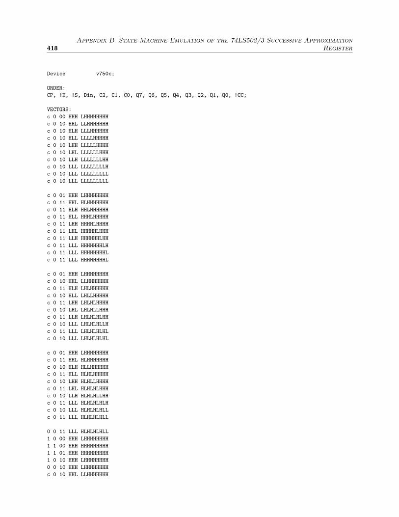
418Appendix B. State-Machine Emulation of the 74LS502/3 Successive-Approximation
Register
Device v750c;
ORDER:
CP, !E, !S, Din, C2, C1, C0, Q7, Q6, Q5, Q4, Q3, Q2, Q1, Q0, !CC;
VECTORS:
c 0 00 HHH LHHHHHHHH
c 0 10 HHL LLHHHHHHH
c 0 10 HLH LLLHHHHHH
c 0 10 HLL LLLLHHHHH
c 0 10 LHH LLLLLHHHH
c 0 10 LHL LLLLLLHHH
c 0 10 LLH LLLLLLLHH
c 0 10 LLL LLLLLLLLH
c 0 10 LLL LLLLLLLLL
c 0 10 LLL LLLLLLLLL
c 0 01 HHH LHHHHHHHH
c 0 11 HHL HLHHHHHHH
c 0 11 HLH HHLHHHHHH
c 0 11 HLL HHHLHHHHH
c 0 11 LHH HHHHLHHHH
c 0 11 LHL HHHHHLHHH
c 0 11 LLH HHHHHHLHH
c 0 11 LLL HHHHHHHLH
c 0 11 LLL HHHHHHHHL
c 0 11 LLL HHHHHHHHL
c 0 01 HHH LHHHHHHHH
c 0 10 HHL LLHHHHHHH
c 0 11 HLH LHLHHHHHH
c 0 10 HLL LHLLHHHHH
c 0 11 LHH LHLHLHHHH
c 0 10 LHL LHLHLLHHH
c 0 11 LLH LHLHLHLHH
c 0 10 LLL LHLHLHLLH
c 0 11 LLL LHLHLHLHL
c 0 10 LLL LHLHLHLHL
c 0 01 HHH LHHHHHHHH
c 0 11 HHL HLHHHHHHH
c 0 10 HLH HLLHHHHHH
c 0 11 HLL HLHLHHHHH
c 0 10 LHH HLHLLHHHH
c 0 11 LHL HLHLHLHHH
c 0 10 LLH HLHLHLLHH
c 0 11 LLL HLHLHLHLH
c 0 10 LLL HLHLHLHLL
c 0 11 LLL HLHLHLHLL
0 0 11 LLL HLHLHLHLL
1 0 00 HHH LHHHHHHHH
1 1 00 HHH HHHHHHHHH
1 1 01 HHH HHHHHHHHH
1 0 10 HHH LHHHHHHHH
0 0 10 HHH LHHHHHHHH
c 0 10 HHL LLHHHHHHH
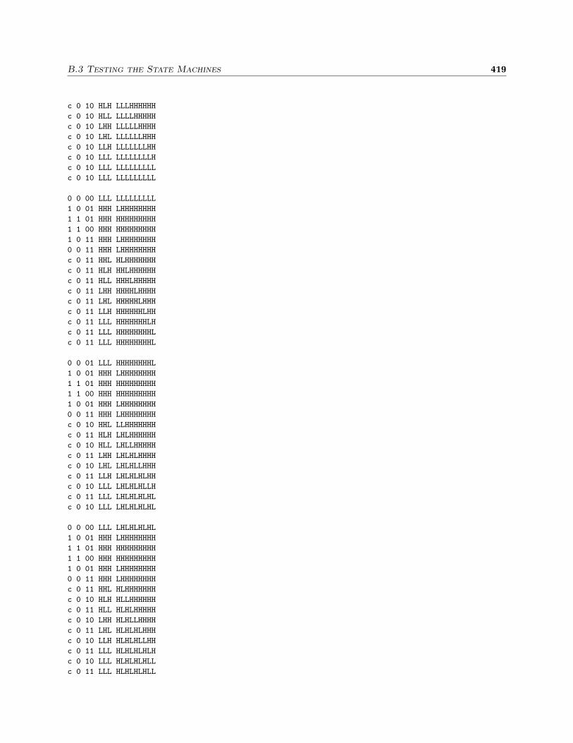
B.3 Testing the State Machines 419
c 0 10 HLH LLLHHHHHH
c 0 10 HLL LLLLHHHHH
c 0 10 LHH LLLLLHHHH
c 0 10 LHL LLLLLLHHH
c 0 10 LLH LLLLLLLHH
c 0 10 LLL LLLLLLLLH
c 0 10 LLL LLLLLLLLL
c 0 10 LLL LLLLLLLLL
0 0 00 LLL LLLLLLLLL
1 0 01 HHH LHHHHHHHH
1 1 01 HHH HHHHHHHHH
1 1 00 HHH HHHHHHHHH
1 0 11 HHH LHHHHHHHH
0 0 11 HHH LHHHHHHHH
c 0 11 HHL HLHHHHHHH
c 0 11 HLH HHLHHHHHH
c 0 11 HLL HHHLHHHHH
c 0 11 LHH HHHHLHHHH
c 0 11 LHL HHHHHLHHH
c 0 11 LLH HHHHHHLHH
c 0 11 LLL HHHHHHHLH
c 0 11 LLL HHHHHHHHL
c 0 11 LLL HHHHHHHHL
0 0 01 LLL HHHHHHHHL
1 0 01 HHH LHHHHHHHH
1 1 01 HHH HHHHHHHHH
1 1 00 HHH HHHHHHHHH
1 0 01 HHH LHHHHHHHH
0 0 11 HHH LHHHHHHHH
c 0 10 HHL LLHHHHHHH
c 0 11 HLH LHLHHHHHH
c 0 10 HLL LHLLHHHHH
c 0 11 LHH LHLHLHHHH
c 0 10 LHL LHLHLLHHH
c 0 11 LLH LHLHLHLHH
c 0 10 LLL LHLHLHLLH
c 0 11 LLL LHLHLHLHL
c 0 10 LLL LHLHLHLHL
0 0 00 LLL LHLHLHLHL
1 0 01 HHH LHHHHHHHH
1 1 01 HHH HHHHHHHHH
1 1 00 HHH HHHHHHHHH
1 0 01 HHH LHHHHHHHH
0 0 11 HHH LHHHHHHHH
c 0 11 HHL HLHHHHHHH
c 0 10 HLH HLLHHHHHH
c 0 11 HLL HLHLHHHHH
c 0 10 LHH HLHLLHHHH
c 0 11 LHL HLHLHLHHH
c 0 10 LLH HLHLHLLHH
c 0 11 LLL HLHLHLHLH
c 0 10 LLL HLHLHLHLL
c 0 11 LLL HLHLHLHLL


Appendix C
Gallery of Characteristic Curves
This appendix presents a haphazard collection of characterstic curves for discrete semiconductor componentsthat are common, useful, or interesting (or some combination). Data sheets contain this information (andmore), but parameters are specified in various ways, and plots are sometimes drawn in bizarre ways. Thecharacteristic curves, however, contain a lot of information at a glance, and having a collection of similarlyplotted curves makes it easy to visually compare similar components. (How many people can explain thedifference between a 2N3904 and a 2N4401? They’re almost interchangeable, but the curves show that theyhave potentially important differences, such as the larger collector resistance of the 2N4401.)
The characteristic curves here are computed from model parameters used in SPICE simulators. Deviceswith similar functionality are grouped together to make it easier to compare their properties. The calculations(in lieu of data), besides being easier to generate than real data, are useful in capturing the “typical” devicebehaviors, according to manufacturers.
The collection of components is in no way complete or representative of any kind of good engineeringpractice.
Now on to the pretty pictures. . .

422 Appendix C. Gallery of Characteristic Curves
C.1 Diodes
C.1.1 Small-Signal Diodes
1N914 (fast, high conductance, Si)1
The venerable 1N914 (good as a default small-signal diode) has many very similar cousins, including the1N914A, 1N914B, 1N916, 1N916A, 1N916B, 1N4148, and the 1N4448. (To wit: all of these share the samedata sheet.2)
1N914
V(V)0 10.2 0.4 0.6 0.8
I(mA)
0
200
40
80
120
160
1N914
V(V)-110 100-100 -50
I(mA)
0
200
-20
1N5711 (Schottky)3
1N5711
V(V)0 10.2 0.4 0.6 0.8
I(mA)
0
15
10
5
1N5711
V(V)-80 10-70 0
I(mA)
0
15
-5
1Central Semiconductor model: https://www.centralsemi.com/product/partpage2.php?part=1N9142http://www.onsemi.com/pub/Collateral/1N914-D.PDF3Diodes Inc. model: http://ltwiki.org/files/LTspiceIV/Vendor%20List/Diodes%20Incorporated/Spice/spicemodels_
schottky_diodes.txt
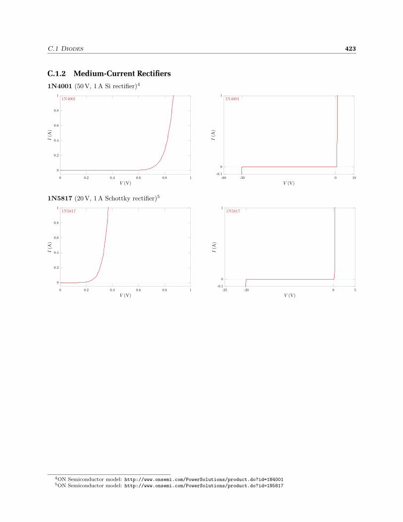
C.1 Diodes 423
C.1.2 Medium-Current Rectifiers
1N4001 (50 V, 1 A Si rectifier)4
1N4001
V(V)0 10.2 0.4 0.6 0.8
I(A)
0
0.2
0.4
0.6
0.8
11N4001
V(V)-60 10-50 0
I(A)
0
-0.1
1
1N5817 (20 V, 1 A Schottky rectifier)5
1N5817
V(V)0 10.2 0.4 0.6 0.8
I(A)
0
0.2
0.4
0.6
0.8
11N5817
V(V)-25 5-20 0
I(A)
0
-0.1
1
4ON Semiconductor model: http://www.onsemi.com/PowerSolutions/product.do?id=1N40015ON Semiconductor model: http://www.onsemi.com/PowerSolutions/product.do?id=1N5817

424 Appendix C. Gallery of Characteristic Curves
C.1.3 High-Current Rectifiers
MR752 (6 A, 200 V power rectifier)6
MR752
V(V)0 10.2 0.4 0.6 0.8
I(A)
0
1
2
3
4
5
6MR752
V(V)-230 30-200 0
I(A)
0
-1
6
MUR1560 (15 A, 600 V power rectifier)7
MUR1560
V(V)0 1.80.2 0.4 0.6 0.8 1 1.2 1.4 1.6
I(A)
0
5
10
15MUR1560
V(V)-650 50-600 0
I(A)
0
15
6ON Semiconductor model: http://www.onsemi.com/PowerSolutions/product.do?id=MR7527ON Semiconductor model: http://www.onsemi.com/PowerSolutions/product.do?id=MUR1560

C.2 Bipolar Junction Transistors 425
C.2 Bipolar Junction Transistors
C.2.1 Small-Signal BJTs
2N2222A (NPN, general purpose)8 The “improved” 2N2222; also PN2222A and P2N2222A.
VCE (V)0 102 4 6 8
IC (
mA
)
12
0
2
4
6
8
10
2N2222A
IBo=o10omA
IBo=o20omA
IBo=o30omA
IBo=o40omA
IBo=o50omA
VCE (V)0 204 8 12 16
IC (
mA
)
0
40
80
120
160
2N2222A
IBo=o200omA
IBo=o400omA
IBo=o600omA
IBo=o800omA
IBo=o1omA
2N2907A (PNP, general purpose; complement to 2N2222A)9
-VCE (V)0 102 4 6 8
-IC (
mA
)
0
4
8
12
16 2N2907A
IBo=o10omA
IBo=o20omA
IBo=o30omA
IBo=o40omA
IBo=o50omA
-VCE (V)0 204 8 12 16
-IC (
mA
)
0
50
100
150
200
250
300 2N2907A
IBo=o200omA
IBo=o400omA
IBo=o600omA
IBo=o800omA
IBo=o1omA
2N3904 (NPN, general purpose)10
VCE (V)0 102 4 6 8
IC (
mA
)
10
0
2
4
6
8
2N3904
IBo=o10omA
IBo=o20omA
IBo=o30omA
IBo=o40omA
IBo=o50omA
VCE (V)0 204 8 12 16
IC (
mA
)
160
0
40
80
120
2N3904
IBo=o200omA
IBo=o400omA
IBo=o600omA
IBo=o800omA
IBo=o1omA
8Central Semiconductor model: https://www.centralsemi.com/product/partpage2.php?part=2N2222A9Central Semiconductor model: https://www.centralsemi.com/product/partpage2.php?part=2N2907A
10Central Semiconductor model: https://www.centralsemi.com/product/partpage2.php?part=2N3904
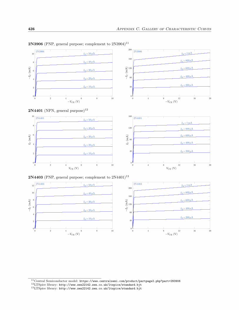
426 Appendix C. Gallery of Characteristic Curves
2N3906 (PNP, general purpose; complement to 2N3904)11
-VCE (V)0 102 4 6 8
-IC (
mA
)
2
4
6
8
10
0
2N3906
IBo=o10omA
IBo=o20omA
IBo=o30omA
IBo=o40omA
IBo=o50omA
-VCE (V)0 204 8 12 16
-IC (
mA
)
200
0
40
80
120
160
2N3906
IBo=o200omA
IBo=o400omA
IBo=o600omA
IBo=o800omA
IBo=o1omA
2N4401 (NPN, general purpose)12
VCE (V)0 102 4 6 8
IC (
mA
)
10
0
2
4
6
8
2N4401
IBo=o10omA
IBo=o20omA
IBo=o30omA
IBo=o40omA
IBo=o50omA
VCE (V)0 204 8 12 16
IC (
mA
)
160
0
40
80
120
2N4401
IBo=o200omA
IBo=o400omA
IBo=o600omA
IBo=o800omA
IBo=o1omA
2N4403 (PNP, general purpose; complement to 2N4401)13
-VCE (V)0 102 4 6 8
-IC (
mA
)
12
2
4
6
8
10
0
2N4403
IBo=o10omA
IBo=o20omA
IBo=o30omA
IBo=o40omA
IBo=o50omA
-VCE (V)0 204 8 12 16
-IC (
mA
)
0
40
80
120
160
200
2N4403
IBo=o200omA
IBo=o400omA
IBo=o600omA
IBo=o800omA
IBo=o1omA
11Central Semiconductor model: https://www.centralsemi.com/product/partpage2.php?part=2N390612LTSpice library: http://www.zen22142.zen.co.uk/ltspice/standard.bjt13LTSpice library: http://www.zen22142.zen.co.uk/ltspice/standard.bjt
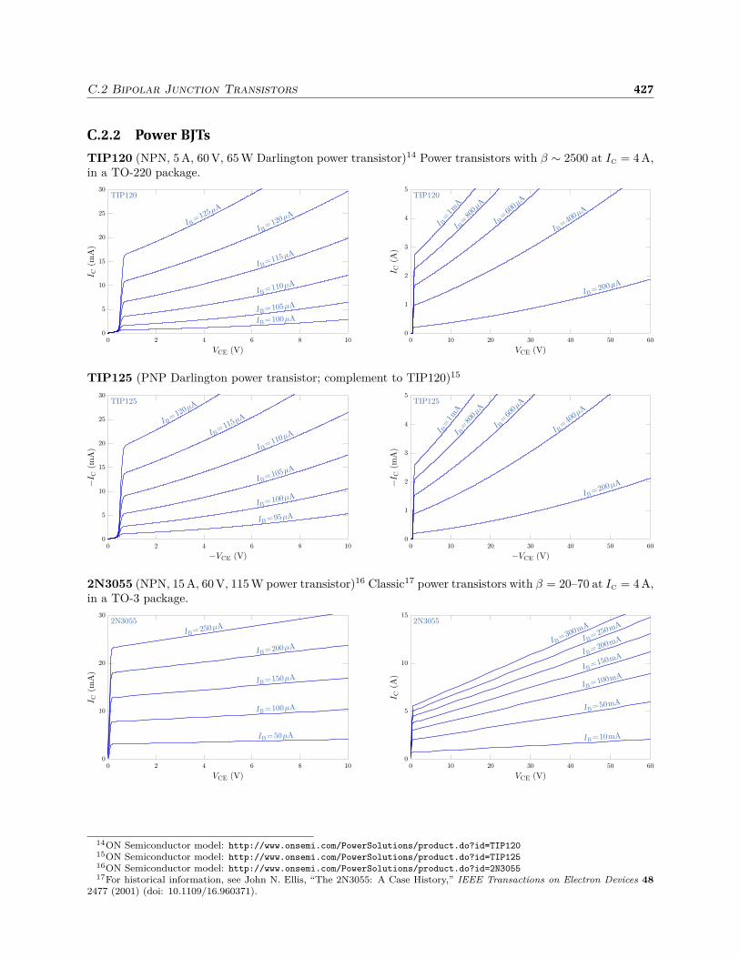
C.2 Bipolar Junction Transistors 427
C.2.2 Power BJTs
TIP120 (NPN, 5 A, 60 V, 65 W Darlington power transistor)14 Power transistors with β ∼ 2500 at IC = 4 A,in a TO-220 package.
VCE (V)0 102 4 6 8
IC (
mA
)
30
0
5
15
25
10
20
TIP120
IBo=o100omAIBo=o105omA
IBo=o110omA
IBo=o115omA
IBo=
o120omAIB
o=o12
5omA
VCE (V)0 6010 20 30 40 50
IC (
A)
5
0
1
2
3
4
TIP120
IBo=o200omA
IBo=
o400om
A
I Bo=
o600om
A
I Bo=
o800om
A
I Bo=
o1omA
TIP125 (PNP Darlington power transistor; complement to TIP120)15
-VCE (V)0 102 4 6 8
-IC (
mA
)
30
0
5
15
25
10
20
TIP125
IBo=o100omA
IBo=o105omA
IBo=o110omAIB
o=o11
5omA
IBo=
o120om
A
IBo=o95omA
-VCE (V)0 6010 20 30 40 50
-IC (
mA
)5
0
1
2
3
4
TIP125
IBo=o200omA
IBo=
o400om
A
I Bo=
o600om
A
I Bo=
o800om
A
I Bo=
o1om
A
2N3055 (NPN, 15 A, 60 V, 115 W power transistor)16 Classic17 power transistors with β = 20–70 at IC = 4 A,in a TO-3 package.
VCE (V)0 102 4 6 8
IC (
mA
)
30
0
10
20
2N3055
IBo=o50omA
IBo=o100omA
IBo=o150omA
IBo=o200omA
IBo=o250omA
VCE (V)0 6010 20 30 40 50
IC (
A)
15
0
5
10
2N3055
IBo=o10omA
IBo=o50omA
IBo=o100omAIBo=o150omAIB
o=o200omAIBo=o250omA
IBo=
o300omA
14ON Semiconductor model: http://www.onsemi.com/PowerSolutions/product.do?id=TIP12015ON Semiconductor model: http://www.onsemi.com/PowerSolutions/product.do?id=TIP12516ON Semiconductor model: http://www.onsemi.com/PowerSolutions/product.do?id=2N305517For historical information, see John N. Ellis, “The 2N3055: A Case History,” IEEE Transactions on Electron Devices 48
2477 (2001) (doi: 10.1109/16.960371).

428 Appendix C. Gallery of Characteristic Curves
MJ2955 (PNP, 15 A, 60 V, 115 W power transistor; complement to 2N3055)18
-VCE (V)0 102 4 6 8
-IC (
mA
)
30
0
10
20
MJ2955
IBo=o50omA
IBo=o100omA
IBo=o150omA
IBo=o200omA
IBo=o250omA
VCE (V)0 6010 20 30 40 50
IC (
A)
15
0
5
10
MJ2955
IBo=o10omA
IBo=o50omA
IBo=o100omA
IBo=o150omAIBo=o200omAIB
o=o250omAIB
o=o300omA
2N6284 (NPN, 20 A, 100 V, 160 W Darlington power transistor)19 Power Darlington transistors in a TO-3package.
VCE (V)0 102 4 6 8
IC (
mA
)
250
0
50
100
150
200
2N6284IBo=o240omA
IBo=o190omA IBo=o200omA
IBo=o210omA
IBo=o220omA
IBo=o230omA
VCE (V)0 10020 40 60 80
IC (
A)
20
0
5
10
15
2N6284
IBo=o1omA
IBo=o4omA
IBo=o8omA
IBo=o12omA
IBo=o16omAIBo=o20omA
2N6287 (PNP Darlington power transistor; complement to 2N6284)20
-VCE (V)0 102 4 6 8
-IC (
mA
)
250
0
50
100
150
200
2N6287
IBo=o120omAIBo=o116omA
IBo=o124omA
IBo=o128omA
IBo=o132omAIBo=o136omA
-VCE (V)0 10020 40 60 80
-IC (
A)
20
0
5
10
15
2N6287
IBo=o200omA
IBo=o500omA
IBo=o1omA
IBo=o2omA
IBo=
o4omA
IBo=
o6omA
IBo=
o8omA
18ON Semiconductor model: http://www.onsemi.com/PowerSolutions/product.do?id=MJ295519ON Semiconductor model: http://www.onsemi.com/PowerSolutions/product.do?id=2N628420ON Semiconductor model: http://www.onsemi.com/PowerSolutions/product.do?id=2N6287
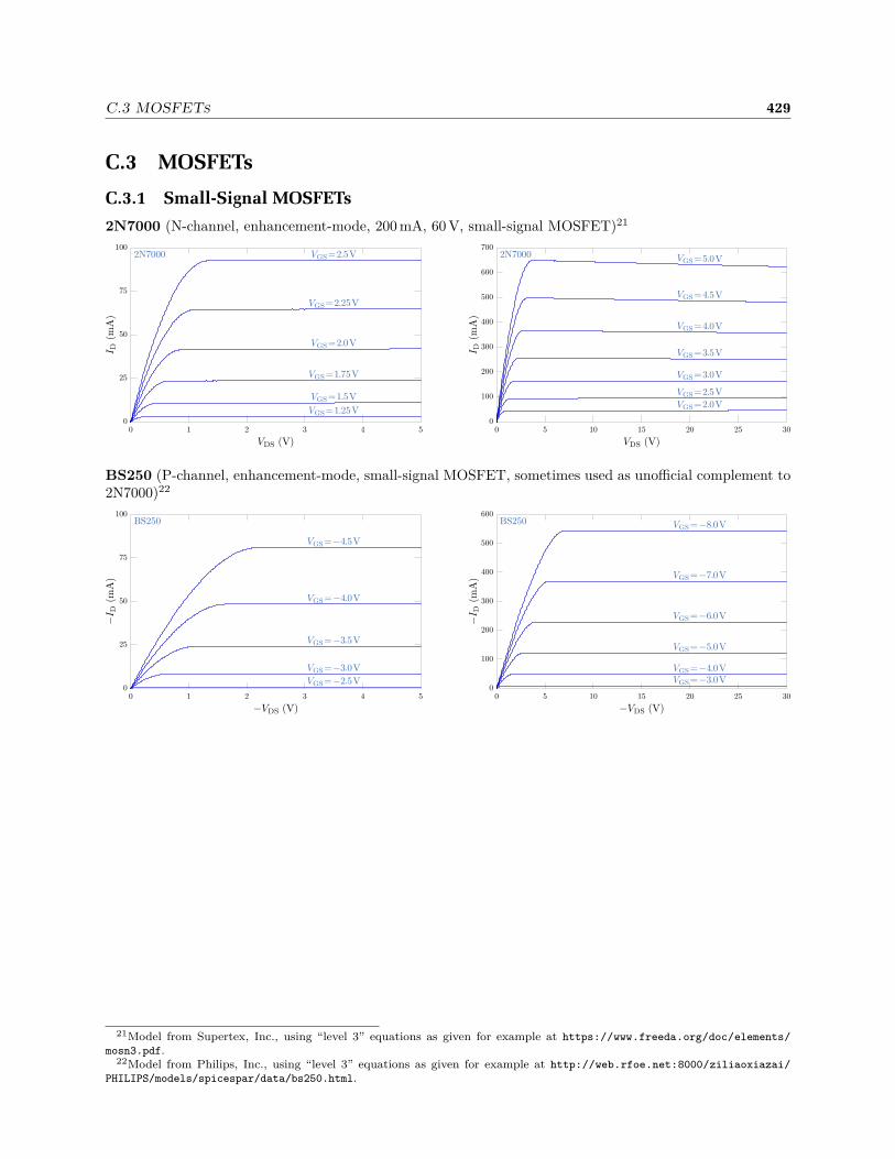
C.3 MOSFETs 429
C.3 MOSFETs
C.3.1 Small-Signal MOSFETs
2N7000 (N-channel, enhancement-mode, 200 mA, 60 V, small-signal MOSFET)21
VDS (V)0 51 2 3 4
ID (
mA
)
100
0
50
25
75
VGSo=o1.25oV
VGSo=o1.5oV
VGSo=o1.75oV
VGSo=o2.0oV
VGSo=o2.25oV
VGSo=o2.5oV2N7000
VDS (V)0 305 10 15 20 25
ID (
mA
)
700
0
100
200
300
400
500
600
VGSo=o5.0oV
VGSo=o4.5oV
VGSo=o2.0oV
VGSo=o2.5oV
VGSo=o3.0oV
VGSo=o3.5oV
VGSo=o4.0oV
2N7000
BS250 (P-channel, enhancement-mode, small-signal MOSFET, sometimes used as unofficial complement to2N7000)22
-VDS (V)0 51 2 3 4
-ID (
mA
)
100
0
50
25
75
VGSo=o-2.5oV
VGSo=o-3.0oV
VGSo=o-3.5oV
VGSo=o-4.0oV
VGSo=o-4.5oV
BS250
-VDS (V)0 305 10 15 20 25
-ID (
mA
)
600
0
100
200
300
400
500
VGSo=o-3.0oVVGSo=o-4.0oV
VGSo=o-5.0oV
VGSo=o-6.0oV
VGSo=o-7.0oV
VGSo=o-8.0oVBS250
21Model from Supertex, Inc., using “level 3” equations as given for example at https://www.freeda.org/doc/elements/
mosn3.pdf.22Model from Philips, Inc., using “level 3” equations as given for example at http://web.rfoe.net:8000/ziliaoxiazai/
PHILIPS/models/spicespar/data/bs250.html.


Index
1/f noise, 228LC frequency, 66Q factor, 66–68RC time, 56, 142AND gate, 272
3-input, 273NAND gate, 272NOR gate, 272NOT gate, 271OR gate, 272XNOR gate, 273XOR gate, 272–273, 278–279
in terms of NAND gates, 2791.5KE400A, 1581N4001, 801N4733, 821N5711, 801N5819, 1581N914B, 802’s complement convention, 270–27122V10, 335, 4092N3904, 119–1233-dB point, 604046 (PLL), 388555 timer, 361–364, 367–368
astable multivibrator, 362–363frequency modulation, 363–364monostable multivibrator, 365–366
6116 SRAM, 33074121 monostable multivibrator, 366–367741C, 189, 198, 200, 206
74138, 31074139, 31674150, 31074151, 309–31074154, 31074251, 311
absolute-value amplifierop-amp, 248–249
absorption theorems, 278, 284active rectifier
op-amp, 241AD594, 313AD985L (DDS), 389ADC, 373, 376–380address bus, 330aliasing, 374amplifier
common-cathode, 170–177analog computer
op-amp, 235–236analog switch, 312
MOSFET, 150–151, 200op-amp, 255
analog-to-digital conversion, 373, 376–380analog-to-digital converter, 353anode, 77anti-aliasing filter, 374associative, 277astable multivibrator, 362–363
made from one-shots, 368–369ATF22V10C, 335, 409ATF750C, 335, 413
band-pass amplifierop-amp, 253–254
bandwidth, 216–221beam power tube, 178bias network, 100–102BiCMOS, 301binary arithmetic, 269–271
power of 2, 274binary logic, 269binary operation, 277bipolar junction transistor, 91–137, 294
as switch, 95–96current-control model, 108Darlington pair, 136–137forward-active mode, 96hybrid model, 123push–pull pair, 116–119saturation, 95–96, 130
bistable, 319bit, 269bit-shift operator, 275–276
431

432 Index
Boltzmann constant, 81Boolean algebra, 277–289bootstrapping, 129BUF634, 219buffer
level-shifting, 304–305buffer gate, 271
capacitance, 53capacitor, 53–57, 73cascode amplifier, 128, 137cathode, 77, 167–168
directly heated, 167filamentary, 167heated, 167indirectly heated, 167
characteristic curvesbipolar transistor, 119–123
charge, 23Child–Langmuir Law, 168chip select, 330Clapton, Eric, 127class-A amplifier, 117class-AB amplifier, 117class-B amplifier, 117clipping, 104closed-loop mode, 190CM600HA-24A, 157CMOS, 142, 300–303CMOS logic, 300–303CMOS switch, 312coaxial cable, 204Cockroft–Walton multiplier, 86–87common-cathode amplifier, 170–177common-emitter amplifier, 102–104, 114–116, 131–
134common-mode gain factor, 107common-mode rejection ratio (CMRR), 107–108, 150,
201, 208common-mode signal, 105common-source amplifier, 147–149commutative, 277comparator, 189–190, 221–224
open-collector output, 222, 354Schmitt trigger, 222–223, 355–358
compensation, 219–221complex notation, 57–58complex PLD, 335compliance, 100conductance, 30–32, 41, 50–51control
integral, 264–265PI, 265
PID, 265–266proportional, 262–264
control grid, 169control theory
linear, 261–266controller, 261counter
asynchronous, 323–324backwards divide-by-3, 338–339divide-by-2, 323divide-by-2-or-3, 339–340divide-by-3, synchronous, 326–327divide-by-3-with-hold, 327–328, 332–333divide-by-4, up/down, 328, 344ripple, 323–324
coupled oscillators, 68–71coupling coefficient
for inductors, 69CPLD, 335crossover distortion, 117, 218current, 23current mirror, 110–112, 133–134
improved Wilson, 129current source
for laser diode, 255–257Howland, 247–248JFET, 146op-amp, 246, 255–259transistor, 99–102
DAC, 373–376, 380data bus, 330DDS, 389De Morgan’s theorems, 278debounced switch, 320–321delta–star transformation, 41–43demultiplexer, 310–316
analog, 311–315DEMUX, 310–316depletion zone, 79desert island, 316DG407, 312DG412, 312DIAC, 153–155differential amplifier
JFET, 149–150op-amp, 194, 201, 246–247transistor, 104–108
differential gain factor, 106differential signal, 105differentiator, 73
op-amp, 194–197digital electronics, 269

Index 433
digital logic, 269digital-to-analog conversion, 373–376, 380dimmer
for lighting, 154–155diode, 77–90
capacitance, 88forward voltage drop, 80forward-biased, 77ideal, 77ideality factor, 81reverse-biased, 77reverse-breakdown voltage, 81reverse-leakage current, 81Schottky, 85–86semiconductor, 77–82TVS, 158vacuum, 77, 167–169vacuum full-wave rectifier, 168–169Zener, 82–83, 88, 158
diode law, 81–82diode logic, 292–293direct digital synthesis, 389distributive, 277DL, 292–293DRAM, 331droop, 264duty cycle, 364, 367–368dynamic RAM, 331
Early effect, 113, 120–121, 124, 137Early voltage, 113Ebers–Moll model, 108–114, 119–123EEPROM, 331electromotive force (EMF), 23electronically erasable PROM, 331emitter degeneration, 115emitter follower, 96–99EPROM, 331erasable PROM, 331Eric Clapton Stratocaster, 127error, 262exponential amplifier
op-amp, 252–253
Farad, 53feedback
in BJT amplifier(, 136in BJT amplifier), 136
feedback control, 261–266feedback signal, 262Fender Musical Instruments, 127FET, 139–151, 162–165FGA60N65SMD, 157
field-effect transistor, 139–151, 162–165CMOS, 142IGFET, 141JFET, 139–141, 162–164MOSFET, 141–142threshold voltage, 140
filterhigh-pass, 61–62low-pass, 59–61, 63
filtersop-amp, 194–200
first-order loop, 388fixed-point notation, 269flicker noise, 228flip-flop, 319–323, 335–338
clocked, 321D-type, 321–322, 328D-type, edge-triggered, 322debounced switch, 320–321JK, 322–323memory, 324–325pulse-area stabilizer, 337–338register, 324–325ripple counter, 323–324SR, 319
floating-point notation, 269fluence, 200flyback transformer, 127frequency, 57frequency modulation
in 555 timer, 363–364full width at half maximum , 67full-wave rectifier, 84–85, 88fundamental charge, 81
gain, 102gain factor
common-mode, 107gain factor differential, 106gain–bandwidth product (GBWP), 217GI754, 80goal, 261Gray code, 280grid, 169
control, 169screen, 177suppressor, 178
ground loop, 204ground plane, 210grounded-emitter amplifier, 114–116grounded-emitter amplifier(, 135grounded-emitter amplifier), 136guitar preamp

434 Index
op-amp, 238–241Gummel–Poon model, 121–123gyrator
op-amp, 236–238
half-wave rectifier, 83–84, 88harmonic oscillator
damped, forced, 265hexagon from hell, 44high-pass filter, 61–62
cascaded, 74–75hole, 78Howland current source, 247–248hysteresis, 319
IGBT, 155–161IGFET, 141impedance, 59impedance-matching condition, 30inductive load
transistor switch, 124–125input bias current, 198–200, 206–208input impedance, 29
through transistor, 97–99input offset current, 208input offset voltage, 200instrumentation amplifier
ac-coupled, hi-Z input, 205–206differential receiver, 204–205op-amp, 200–206thermocouple, 203–204
insulated-gate bipolar transistor, 155–161integrating factor, 55integrator, 54–56
op-amp, 195–200intrinsic emitter resistance, 108, 110inverter, 158–161, 271
Tesla coil, 160–161inverting amplifier
op-amp, 191–192, 214–216IRF1405, 157IXYN80N90C3H1, 157, 158
JFET, 139–141, 162–164common-source amplifier, 147–149current source, 146differential amplifier, 149–150source follower, 146–147
Johnson–Nyquist noise, 226–228joule thief, 125–126junction, 78
Karnaugh map, 280–285, 288–289Kirchoff’s laws, 24–25
Lagrange multiplier, 34Lambert W function, 90level-shifting buffer, 304–305LF411, 189linear algebra, 30–32, 50–51little-h notation, 123–124LM311, 222, 223LM399, 82logarithmic amplifier
op-amp, 247logic
three-state, 311logic gates, 271–273, 291–307long-tailed pair, 105low-pass filter, 59–61
in PLL, 387inductor, 73–74phase, 63two-pole capacitor–inductor, 75
maximum-value amplifierop-amp, 249–250
memory, 324–325, 328–331, 339state machines with, 331–335
mho (), 142microprocessor, 333Miller effect, 113–114, 134–135, 137Millman’s theorem, 43mixer, 389
rf, 387monostable multivibrator, 364–367
74121, 366–367MOSFET, 141–142, 297–303MR752, 80multiplexer, 309–316
analog, 311–315multivibrator
astable, 362–363monostable, 364–367
mutual inductance, 68MUX, 309–316
n-type carrier, 78n-type semiconductor, 78negative feedback, 104, 190negative-feedback mode, 190negative-impedance converter
op-amp, 250–251NMOS, 298–299NMOS logic, 298–299noise immunity, 104non-Ohmic, 77noninverting amplifier

Index 435
op-amp, 192–193, 211–214nonlinear, 77Norton’s theorem, 37notch filter, 76Nyquist frequency, 373
octave, 60Ohm’s law, 23–24ohmic contact, 85one-shot, 364–367op-amp, 112
current feedback, 208, 212golden rules, 190voltage feedback, 208, 212
op-amps, 127–129, 163–164, 189–259stability, 257–259transistor internals of AD829, 127–129transistor internals of TL082, 163–164
OPA111B, 189OPA602C, 198, 200open-collector output, 222, 354open-loop gain, 189
finite, 211–216open-loop mode, 189operational amplifier
absolute-value amplifier, 248–249active rectifier, 241analog computer, 235–236band-pass amplifier, 253–254current source, 246, 256–259differential amplifier, 194, 201, 246–247differentiator, 194–197exponential amplifier, 252–253filters, 194–200guitar preamp, 238–241gyrator, 236–238Howland current source, 247–248instrumentation amplifier, 200–206integrator, 195–200inverting amplifier, 191–192, 214–216logarithmic amplifier, 247maximum-value amplifier, 249–250negative-impedance converter, 250–251noninverting amplifier, 192–193, 211–214phase-shift oscillator, 224–225photodiode amplifier, 245–246pulse-area stabilizer, 241–243relaxation oscillator, 223–224single-supply, 209stability, 192summing amplifier, 193–194transimpedance amplifier, 245–246, 252unity-gain buffer, 190–191
operational amplifiers, 127–129, 163–164, 189–259bandwidth, 216–221comparator, 221–224compensation, 219–221noise analysis, 225–234
output admittance, 113, 123, 133output enable, 330output impedance, 29
through transistor, 97–99output swing, 189
p-n junction, 78p-type carrier, 78p-type semiconductor, 78P6KE20CA, 158PAL, 326path to ground
dc, 199pentode
triode connection, 183–184phase detector, 386
type I, 386type II, 386
phase shift, 62–63and power, 63–65
phase-locked loop, 385–392phase-shift oscillator
op-amp, 224–225photodiode, 245–246
amplifier instability, 252PID control, 261–266pink noise, 228PLA, 326plant, 261plate
vacuum-tube, 167plate resistance, 173PLD, 326, 335PLL, 385–392PMOS, 299–300PMOS logic, 299–300potential, 23
difference, 23power, 24power factor, 65power-supply rejection ratio (PSRR), 209printed circuit board (PCB), 210programmable array logic, 326programmable logic array, 326programmable logic devices, 326, 335programmable ROM, 331, 333–335PROM, 331, 333–335proportional–integral (PI) control, 265

436 Index
proportional–integral–derivative (PID) control, 265pulse-area stabilizer
op-amp, 241–243, 337–338pulse-width modulation, 364push–pull amplifier, 116–119push-pull amplifier, 217–219
quiescent current, 111
race condition, 282–283, 289RAM, 328–331random-access memory, 328–331reactance
capacitive, 58inductive, 58–59
read enable, 330read-only memory, 331rectifier
active, 241full-wave, 84–85, 88half-wave, 83–84, 88
register, 324–325shift, 325
relaxation oscillatorop-amp, 223–224
resistanceplate, 173
resistor networkmatrix formalism, 30–38, 50–51
resistor-transistor logic, 293–295resistors, 24
parallel, 25–26series, 25voltage divider, 26–29
resonant circuit, 65–68, 72coupled, 68–71
resonant frequency, 66ripple counter, 323–324rms, 64ROM, 331RTL, 293–295
S401E (SCR), 152sample, 269sampling rate, 373sampling theorem, 373saturation current, 81schmactivated, 76schmapacitor, 75–76, 245schmesistor, 47, 244schmesonator, 76Schmitt trigger, 222–223, 355–358Schmohm’s law, 47, 244
Schottky barrier, 85SCR, 151–153screen grid, 177second-order loop, 388secondary emission, 178Seebeck effect, 203semiconductor-controlled rectifier, 151–153sequential logic, 325–328, 331–335, 338–340shift register, 325Shockley, William, 81siemens, 142sign-magntitude convention, 270signed integer, 270–271simple PLD, 335slew rate, 217source follower
JFET, 146–147SPICE, 81SPLD, 335SR flip-flop, 319SRAM, 328–331state diagram, 327–328state machine, 325–328, 331–335, 338–340static RAM, 328–331summing amplifier
op-amp, 193–194superposition theorem, 37–38suppressor grid, 178switch, 291–292
debounced, 320–321SPDT, 292SPST, 291
tank circuit, 65Tesla coil, 68, 72tesla coil
solid-state, 126–127Thévenin’s theorem, 27–30, 32–40
proof, 32–38thermal runaway, 118thermal voltage, 108thermistor, 253thermocouple, 312–315three-state logic, 311thyratron, 153thyristor, 151–155transconductance, 109, 141, 142transfer function
feedback-control loop, 262–263transformer, 68transient-voltage suppressor, 158transimpedance amplifier
op-amp, 252

Index 437
transistorα parameter, 93β parameter, 93bipolar junction, 91–137, 294Darlington pair, 136–137forward current ratio, 123hybrid model, 123input impedance, 123insulated-gate bipolar, 155–161MOSFET, 297–303output admittance, 123reverse voltage ratio, 123
transistor switchinductive load, 124–125
transistor-transistor logic, 295–297transistor-transistor logic (TTL), 269TRIAC, 153–155triode
vacuum, 169–177truth table, 271TTL, 295–297tube, vacuum, 167–187TVS, 158two’s complement convention, 270–271type I phase detector, 386type II phase detector, 386
UCC3732x, 158uninterruptible power supply, 159unity-gain bandwidth, 217unity-gain buffer
op-amp, 190–191unsigned integer, 269–270
vacuum tube, 167–187diode, 167–169triode, 169–177
VCO, 387voltage, 23voltage divider, 26–29, 41voltage follower
op-amp, 190–191voltage multiplier
Cockroft–Walton, 86–87voltage-controlled oscillator, 387
Wheatstone bridge, 253white noise, 227work function, 85write enable, 329, 330
XKCD, 50–51
Zener diode, 82–83, 88, 158