Embed Size (px)
Citation preview
page 1
CSEM, E. Vittoz, 2003
Weak inversion
• Behaviour and model of MOS transistors in weak inversion [1,2,3].
• Examples of analog circuits.
• Exploratory analysis of weak inversion logic [4,5].
Eric A.VittozCSEM, Centre Suisse d'Electronique et de Microtechnique SA
Jaquet-Droz 1, CH 2007 Neuchâtel, [email protected]
WEAK INVERSION IN
ANALOG AND DIGITAL CIRCUITS
CCCD Workshop 2003, Lund, Oct. 2-3
page 2
CSEM, E. Vittoz, 2003
Weak inversion
W,L width, length of the channel
Cox gate capacitance per unit area
UT = kT/q ( = 26 mV at 300°K)V = local non-equilibrium voltage in channel : channel voltage
(quasi-Fermi potential of electrons)• at source end of channel: V = VS• at drain end of channel: V = VD
Qi local mobile inversion charge in channel (electrons)
VT0 gate threshold voltage for V=0.
VS
S D
BVD
VG
VS
ID
G
B
S D
VD
VG
ID
symbols:
p-channel
n-channel
n-channel
MOS TRANSISTOR : DEFINITIONS
DG
SID
VDVG
VSn+ n+
p
B
local substrate
page 3
CSEM, E. Vittoz, 2003
Weak inversion
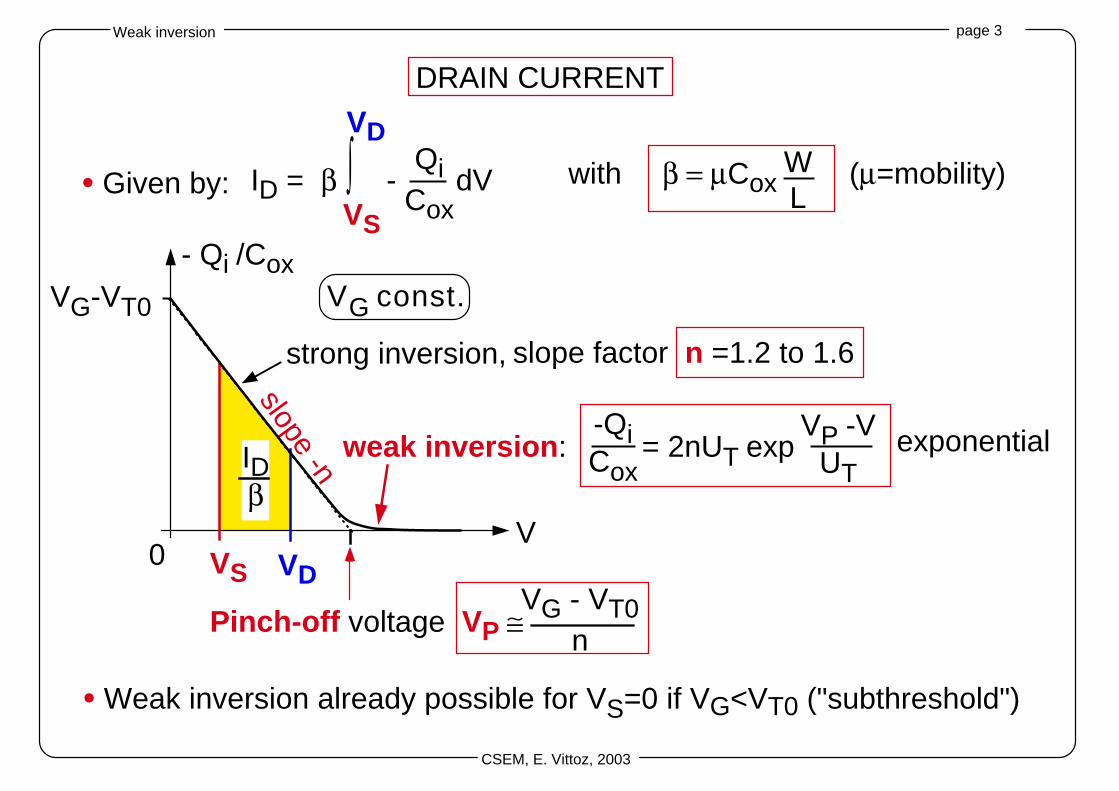
(µ=mobility)with β = µCoxWL
slope -n
- Qi /Cox
VS VD
IDβ
VG const.
V
ID = β - dV∫VS
VDQi
Cox• Given by:
DRAIN CURRENT
• Weak inversion already possible for VS=0 if VG<VT0 ("subthreshold")
VG-VT0
0
Pinch-off voltage VP ≅ VG - VT0
n
strong inversion,
VP -VUT
weak inversion: = 2nUT exp-QiCox
exponential
slope factor n =1.2 to 1.6
page 4
CSEM, E. Vittoz, 2003
Weak inversion
-Qi /Cox
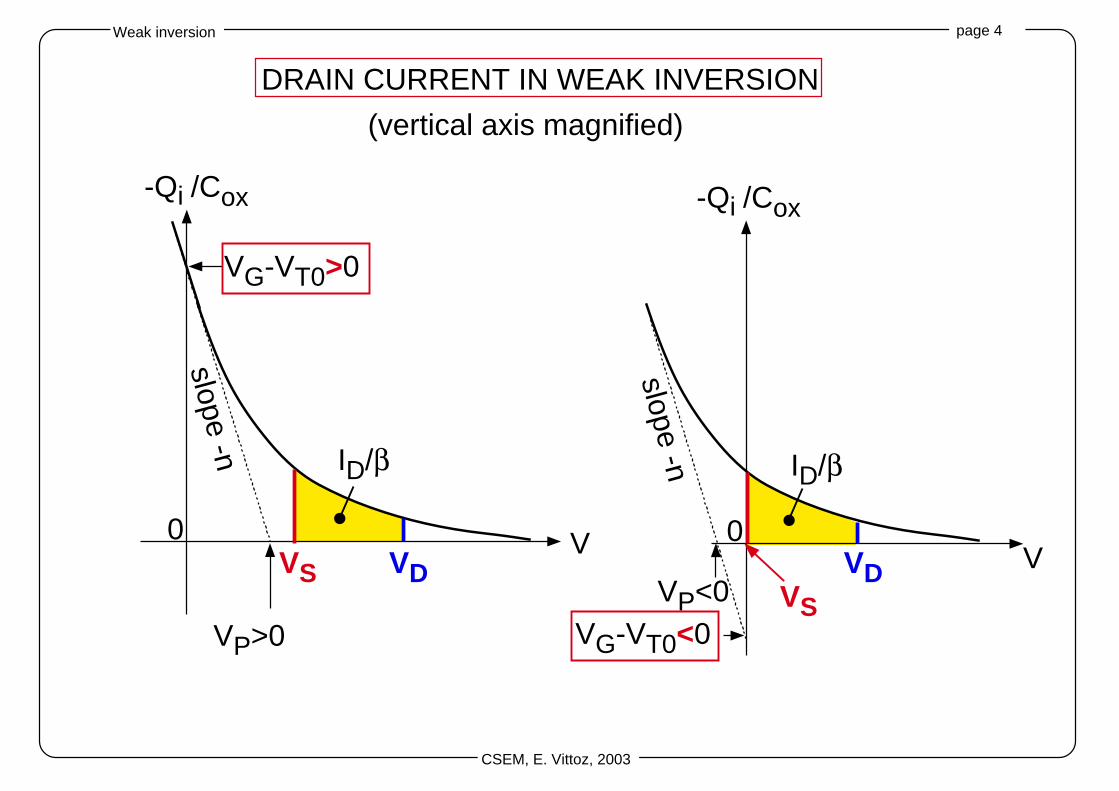
VVP<0
0
slope -n ID/β
VDVS
-Qi /Cox
V
VG-VT0>0
VP>0
0
slope -n ID/β
VDVS
DRAIN CURRENT IN WEAK INVERSION
(vertical axis magnified)
VG-VT0<0
page 5
CSEM, E. Vittoz, 2003
Weak inversion
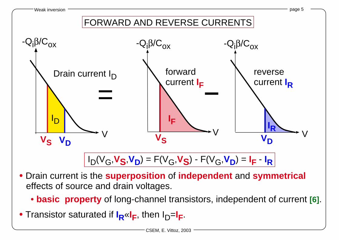
VVD
IR
reversecurrent IR
-Qiβ/Cox
VVS
IF
forwardcurrent IF
-Qiβ/Cox
V
ID
=Drain current ID
VS VD
FORWARD AND REVERSE CURRENTS
-Qiβ/Cox
ID(VG,VS,VD) = F(VG,VS) - F(VG,VD) = IF - IR
• Drain current is the superposition of independent and symmetricaleffects of source and drain voltages.
• basic property of long-channel transistors, independent of current [6].
• Transistor saturated if IR«IF, then ID=IF.
page 6
CSEM, E. Vittoz, 2003
Weak inversion
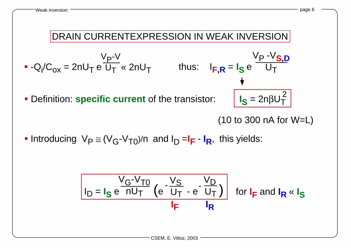
DRAIN CURRENTEXPRESSION IN WEAK INVERSION
VDUT
-VSUT
-nUT
VG-VT0ID = IS e (e - e )
IF IR
for IF and IR « IS
thus: IF,R = IS eVP -VS,D
UT• -Qi/Cox = 2nUT eVP-VUT « 2nUT
• Introducing VP ≅ (VG-VT0)/n and ID =IF - IR, this yields:
• Definition: specific current of the transistor: IS = 2nβUT 2
(10 to 300 nA for W=L)
page 7
CSEM, E. Vittoz, 2003
Weak inversion
ID~ eVSUT
-nUT
VGID ~ e ~ 1-e
VD-VSUT
-ID
slope 1
logIDID0
VSUT
-
logIDID0
slope 1/n
VS, VD const.
VGUT
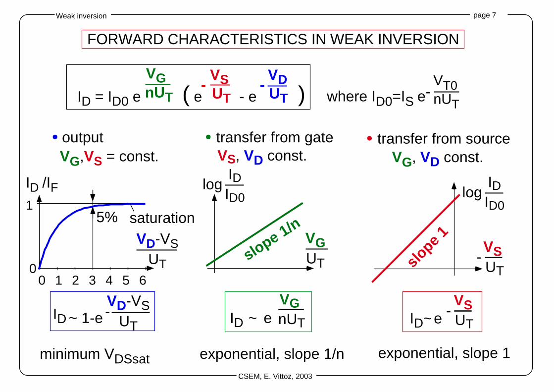
• transfer from gate
1
0
5%
VD-VSUT
ID /IF
saturation
0 1 2 3 4 5 6
• output
FORWARD CHARACTERISTICS IN WEAK INVERSION
VDUT
-VSUT
-nUT
VGID = ID0 e ( e - e )
• transfer from source
minimum VDSsat exponential, slope 1/n exponential, slope 1
where ID0=IS e-VT0nUT
VG, VD const.VG,VS = const.
page 8
CSEM, E. Vittoz, 2003
Weak inversion
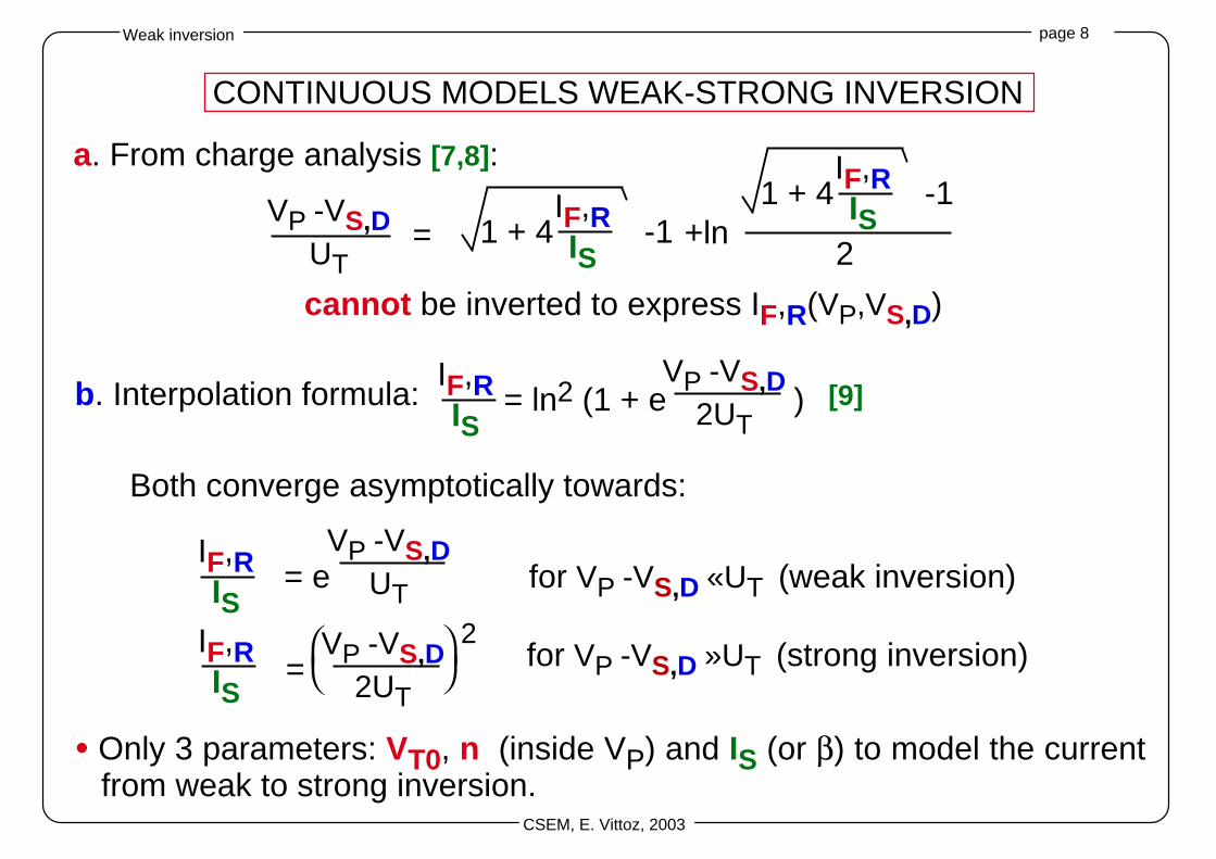
CONTINUOUS MODELS WEAK-STRONG INVERSION
a. From charge analysis [7,8]:
VP -VS,DUT
= 1 + 4 -1 IF,RIS
+ln2
1 + 4 -1 IF,RIS
IF,RIS
cannot be inverted to express IF,R(VP,VS,D)
b. Interpolation formula: VP -VS,D
2UT= ln2 (1 + e )
Both converge asymptotically towards:
IF,RIS
= e for VP -VS,D «UT (weak inversion)
VP -VS,DUT
VP -VS,D2UT
IF,RIS
= for VP -VS,D »UT (strong inversion) 2
• Only 3 parameters: VT0, n (inside VP) and IS (or β) to model the currentfrom weak to strong inversion.
[9]
page 9
CSEM, E. Vittoz, 2003
Weak inversion
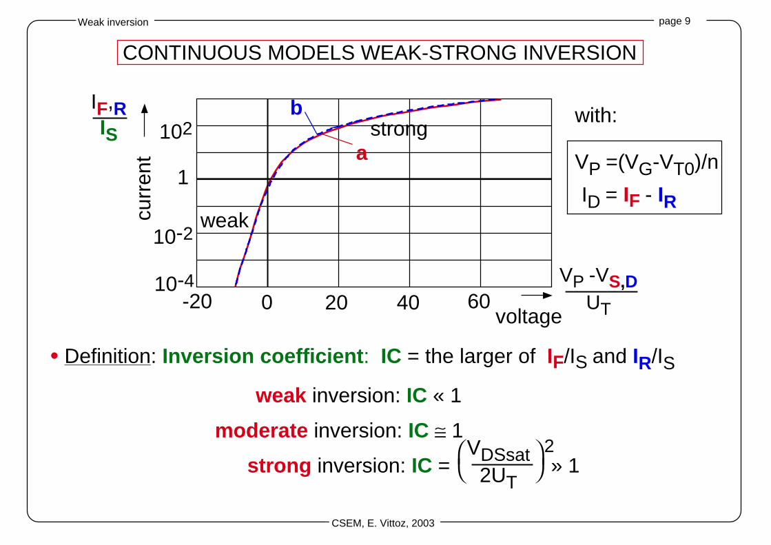
• Definition: Inversion coefficient: IC = the larger of IF/IS and IR/IS
2VDSsat
2UTstrong inversion: IC = » 1
weak inversion: IC « 1
moderate inversion: IC ≅ 1
1
b
a
weak
strong102
10-2
10-4-20 20 40 600
voltage
IF,RIS
curr
ent
VP -VS,DUT
CONTINUOUS MODELS WEAK-STRONG INVERSION
with:
VP =(VG-VT0)/n
ID = IF - IR
page 10
CSEM, E. Vittoz, 2003
Weak inversion
strong inv.0.01 0.1 1 10
0.20
0.40.6
0.81.0
a
b
weak moderate
strong inv.asymptote:
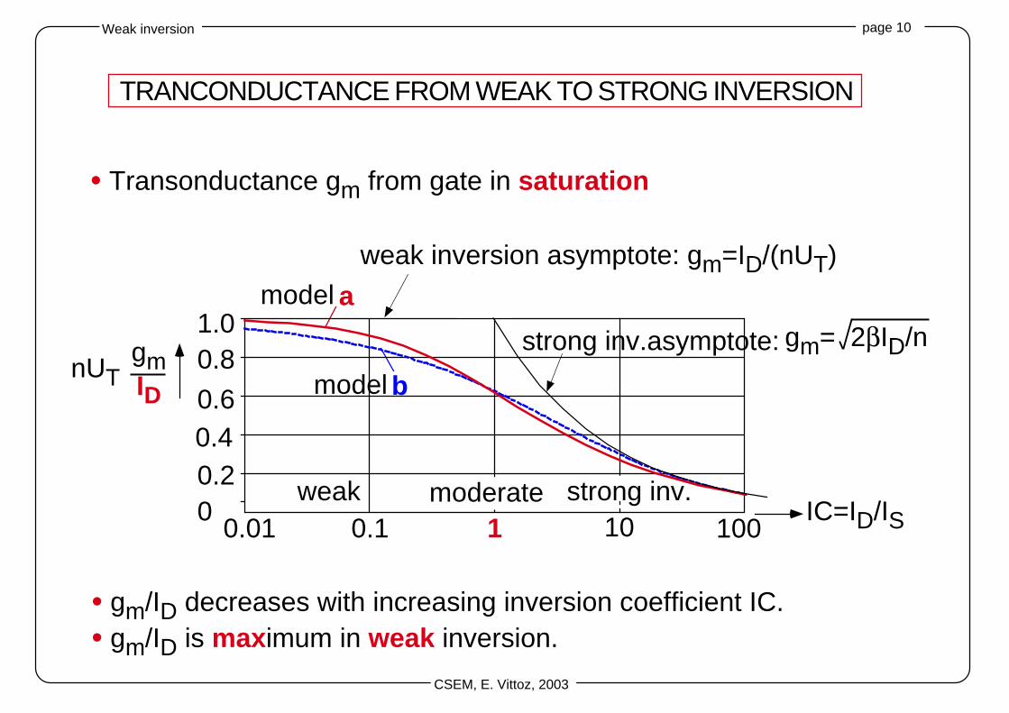
TRANCONDUCTANCE FROM WEAK TO STRONG INVERSION
• Transonductance gm from gate in saturation
gmID
nUT
model
model
IC=ID/IS
gm= 2βID/n
weak inversion asymptote: gm=ID/(nUT)
100
• gm/ID decreases with increasing inversion coefficient IC.• gm/ID is maximum in weak inversion.
page 11
CSEM, E. Vittoz, 2003
Weak inversion
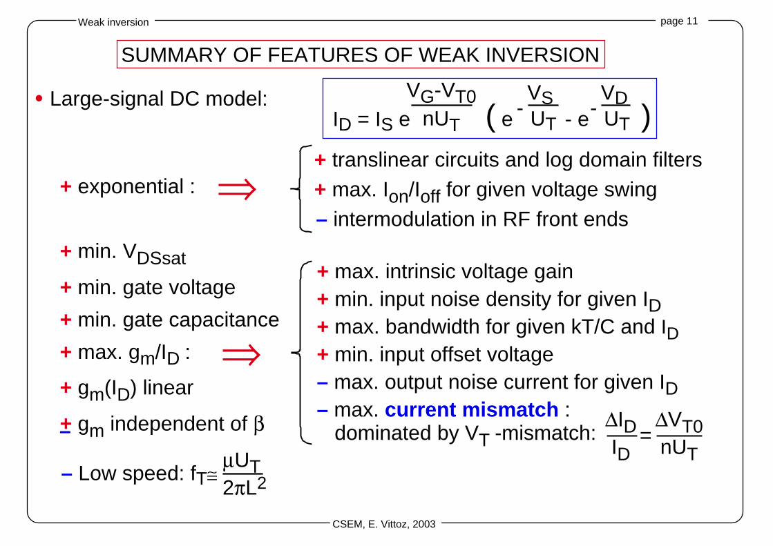
+ exponential :
+ min. VDSsat
+ min. gate voltage
+ min. gate capacitance
+ max. gm/ID :
+ gm(ID) linear
+ gm independent of β
SUMMARY OF FEATURES OF WEAK INVERSION
µUT2πL2
VDUT
-VSUT
-VG-VT0
nUTID = IS e ( e - e )• Large-signal DC model:
+ max. intrinsic voltage gain+ min. input noise density for given ID+ max. bandwidth for given kT/C and ID+ min. input offset voltage– max. output noise current for given ID– max. current mismatch :
dominated by VT -mismatch:
⇒
+ max. Ion/Ioff for given voltage swing+ translinear circuits and log domain filters
– intermodulation in RF front ends⇒
–
– Low speed: fT≅
∆IDID
∆VT0nUT
=
page 12
CSEM, E. Vittoz, 2003
Weak inversion
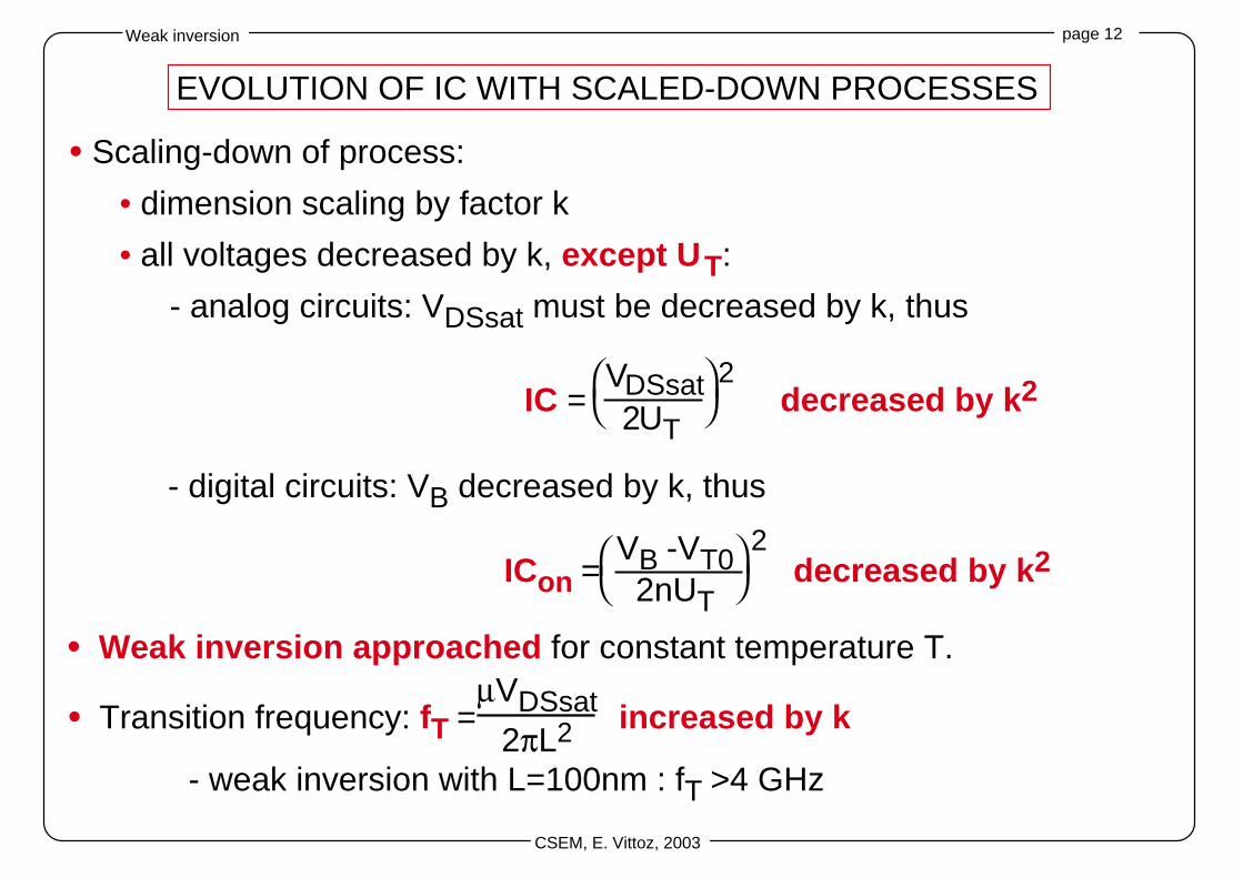
• Weak inversion approached for constant temperature T.
VDSsat2UT
2 IC = decreased by k2
EVOLUTION OF IC WITH SCALED-DOWN PROCESSES
• Scaling-down of process:
• dimension scaling by factor k
• all voltages decreased by k, except UT:
- analog circuits: VDSsat must be decreased by k, thus
- digital circuits: VB decreased by k, thus
VB -VT02nUT
2ICon = decreased by k2
• Transition frequency: fT = increased by kµVDSsat
2πL2
- weak inversion with L=100nm : fT >4 GHz
page 13
CSEM, E. Vittoz, 2003
Weak inversion
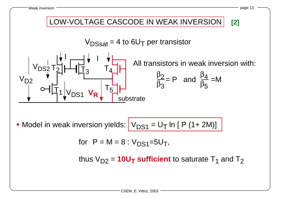
T1
T2 T3 T4
T5
II
VRVDS1
VD2
VDS2
substrate
VDS1 = UT ln [ P (1+ 2M)]
for P = M = 8 : VDS1=5UT,
LOW-VOLTAGE CASCODE IN WEAK INVERSION
• Model in weak inversion yields:
VDSsat = 4 to 6UT per transistor
thus VD2 = 10UT sufficient to saturate T1 and T2
= P and =Mβ2β3
β4β5
All transistors in weak inversion with:
[2]
page 14
CSEM, E. Vittoz, 2003
Weak inversion
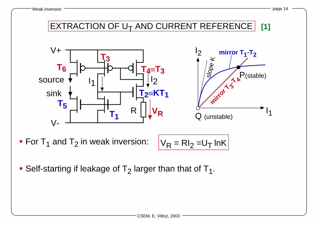
EXTRACTION OF UT AND CURRENT REFERENCE
VR = RI2 =UT lnK
I2
I1Q (unstable)
P(stable)
mirror T1-T2
mirr
or T3
-T 4
slop
e K
T1
T2≡KT1T5
T4≡T3
T3T6
source
sink
I1 I2
R VR
V+
V-
• For T1 and T2 in weak inversion:
• Self-starting if leakage of T2 larger than that of T1.
[1]
page 15
CSEM, E. Vittoz, 2003
Weak inversion
T4
V-
T1
T3
T5
T6V+
T7
T9
II
I
T2
I
VR
T8
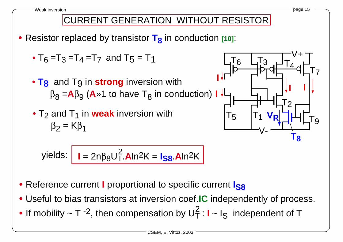
CURRENT GENERATION WITHOUT RESISTOR
• Resistor replaced by transistor T8 in conduction [10]:
• T2 and T1 in weak inversion with β2 = Kβ1
• T6 =T3 =T4 =T7 and T5 = T1
• T8 and T9 in strong inversion with β8 =Aβ9 (A»1 to have T8 in conduction)
I = 2nβ8UT.Aln2K = IS8.Aln2K2yields:
• Reference current I proportional to specific current IS8
• Useful to bias transistors at inversion coef.IC independently of process.
• If mobility ~ T -2, then compensation by UT : I ~ IS independent of T 2
page 16
CSEM, E. Vittoz, 2003
Weak inversion
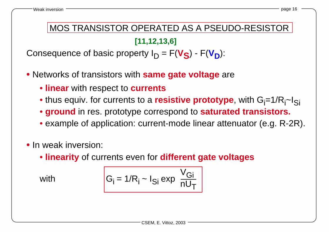
MOS TRANSISTOR OPERATED AS A PSEUDO-RESISTOR
Consequence of basic property ID = F(VS) - F(VD):
• Networks of transistors with same gate voltage are
• linear with respect to currents• thus equiv. for currents to a resistive prototype, with Gi=1/Ri~ISi• ground in res. prototype correspond to saturated transistors.• example of application: current-mode linear attenuator (e.g. R-2R).
• In weak inversion:• linearity of currents even for different gate voltages
with Gi = 1/Ri ~ ISi exp VGinUT
[11,12,13,6]
page 17
CSEM, E. Vittoz, 2003
Weak inversion
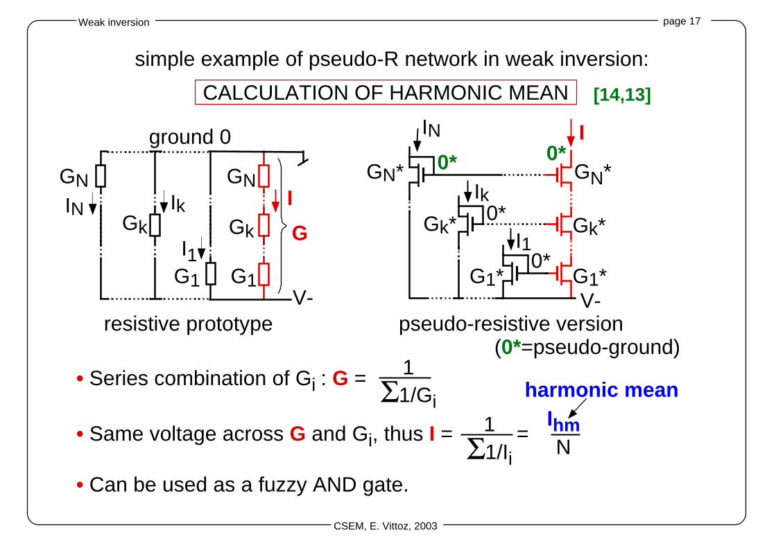
CALCULATION OF HARMONIC MEAN
G1
GN
Gk
ground 0
V-G1
Gk
GNIkIN
I1G
I
I
Ik0*
V-
Gk*
G1*
IN
I1
0* 0*
0*G1*
Gk*
GN*GN*
resistive prototype pseudo-resistive version(0*=pseudo-ground)
• Series combination of Gi : G = 1Σ1/Gi
• Same voltage across G and Gi, thus I = = 1Σ1/Ii
IhmN
harmonic mean
• Can be used as a fuzzy AND gate.
simple example of pseudo-R network in weak inversion:
[14,13]
page 18
CSEM, E. Vittoz, 2003
Weak inversion
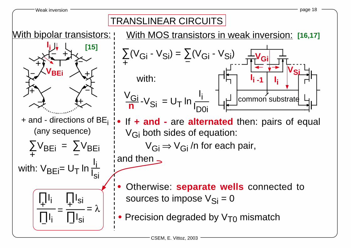
Ii
VBEi
[15]
With bipolar transistors:
∑VBEi = ∑VBEi
with: VBEi= UT lnIiIsi
+ and - directions of BEi
TRANSLINEAR CIRCUITS
∏Ii ∏Isi
∏Ii ∏Isi= = λ
With MOS transistors in weak inversion:
Ii
VGi
VSiIi -1
common substrate
∑(VGi - VSi) = ∑(VGi - VSi)
with:
• Otherwise: separate wells connected tosources to impose VSi = 0
• Precision degraded by VT0 mismatch
• If + and - are alternated then: pairs of equalVGi both sides of equation:
VGi ⇒ VGi /n for each pair,and then
[16,17]
+
+
++
+
-VSi = UT lnIi
ID0i
+
+
++
(any sequence)
VGin
page 19
CSEM, E. Vittoz, 2003
Weak inversion
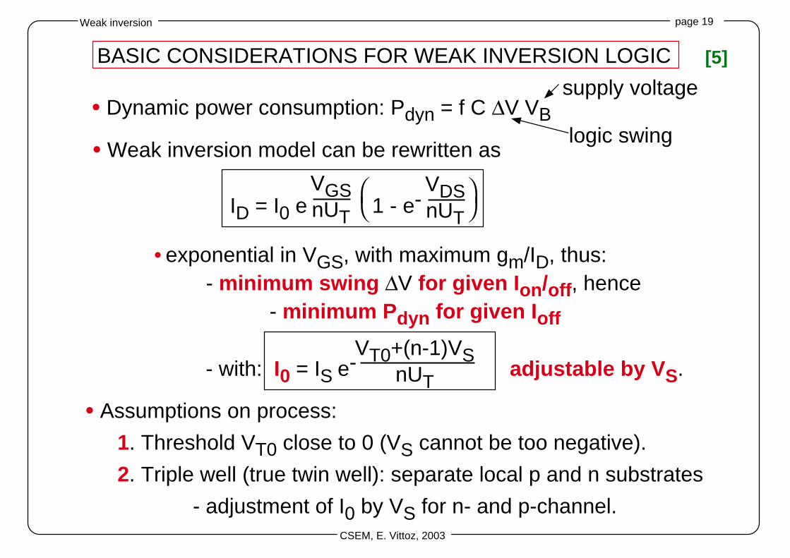
BASIC CONSIDERATIONS FOR WEAK INVERSION LOGIC
• Dynamic power consumption: Pdyn = f C ∆V VB
• exponential in VGS, with maximum gm/ID, thus:- minimum swing ∆V for given Ion/off, hence
- minimum Pdyn for given Ioff
• Assumptions on process:
1. Threshold VT0 close to 0 (VS cannot be too negative).
2. Triple well (true twin well): separate local p and n substrates
- adjustment of I0 by VS for n- and p-channel.
supply voltage
logic swing• Weak inversion model can be rewritten as
ID = I0 e 1 - e-VGSnUT
VDSnUT
- with: I0 = IS e- adjustable by VS. VT0+(n-1)VS
nUT
[5]
page 20
CSEM, E. Vittoz, 2003
Weak inversion
Vi Vo
Ip
InVB
V+
V-
inverter
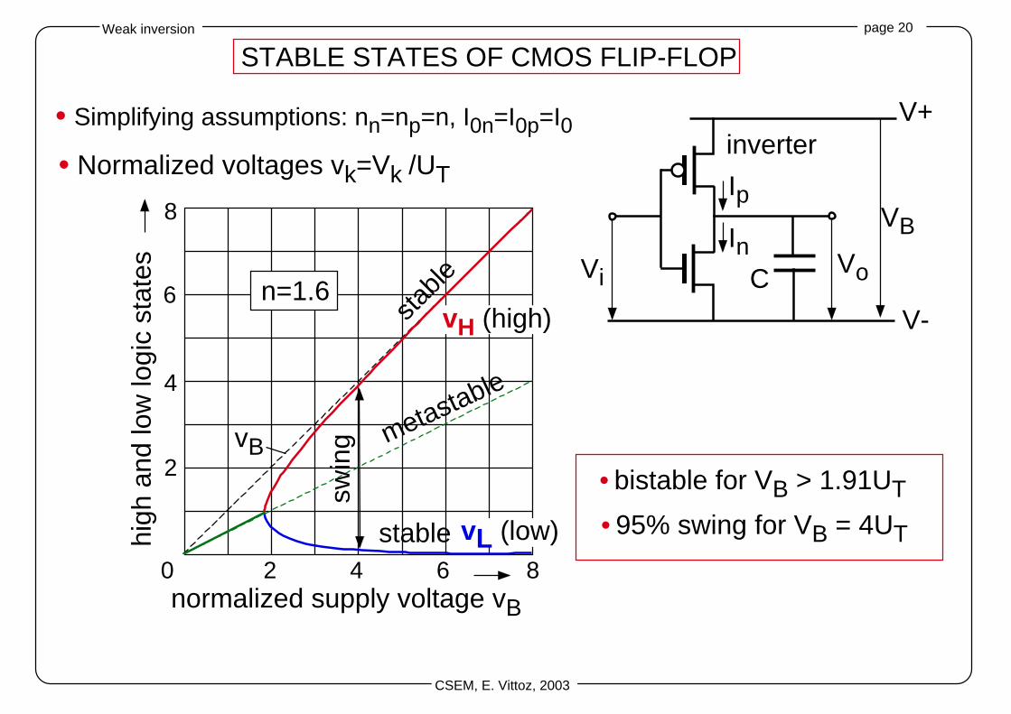
STABLE STATES OF CMOS FLIP-FLOP
• Simplifying assumptions: nn=np=n, I0n=I0p=I0
0 2 4 6
8
2
4
6
8
stable
stable
metastable
vL (low)
vH (high)sw
ingvB
high
and
low
logi
c st
ates
n=1.6
normalized supply voltage vB
• Normalized voltages vk=Vk /UT
• bistable for VB > 1.91UT
• 95% swing for VB = 4UT
C
page 21
CSEM, E. Vittoz, 2003
Weak inversion
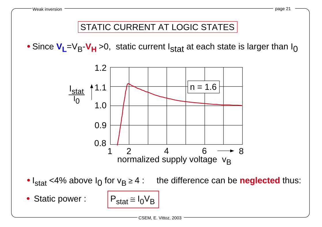
STATIC CURRENT AT LOGIC STATES
• Since VL=VB-VH >0, static current Istat at each state is larger than I0
0.8
0.9
1.0
1.1
1.2
1 2 4 6 8
IstatI0
normalized supply voltage vB
n = 1.6
• Istat <4% above I0 for vB ≥ 4 : the difference can be neglected thus:
• Static power : Pstat ≅ I0VB
page 22
CSEM, E. Vittoz, 2003
Weak inversion
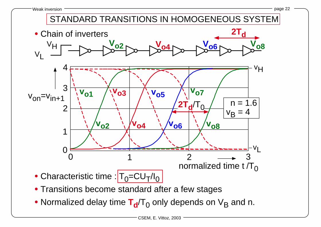
Vo2 Vo4 Vo6 Vo8VHVL
0 1 2 30
1
2
3
4
normalized time t /T0
von=vin+1 n = 1.6vB = 4
vo1
vo2
vo3
vo4
vo5
vo6
vo7
vo8
vH
vL
2Td/T0
• Characteristic time : T0=CUT/I0• Transitions become standard after a few stages
• Normalized delay time Td/T0 only depends on VB and n.
2Td• Chain of inverters
STANDARD TRANSITIONS IN HOMOGENEOUS SYSTEM
page 23
CSEM, E. Vittoz, 2003
Weak inversion
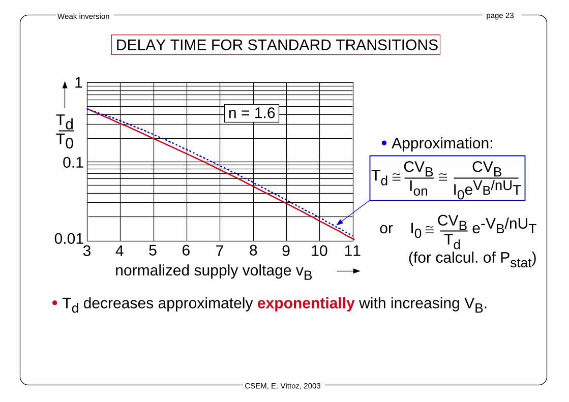
DELAY TIME FOR STANDARD TRANSITIONS
3 4 5 6 7 8 9 10 11
1
0.1
0.01
n = 1.6
normalized supply voltage vB
• Approximation:
Td ≅ ≅ CVBIon
CVBI0eVB/nUT
TdT0
• Td decreases approximately exponentially with increasing VB.
or I0 ≅ e-VB/nUTCVBTd
(for calcul. of Pstat)
page 24
CSEM, E. Vittoz, 2003
Weak inversion
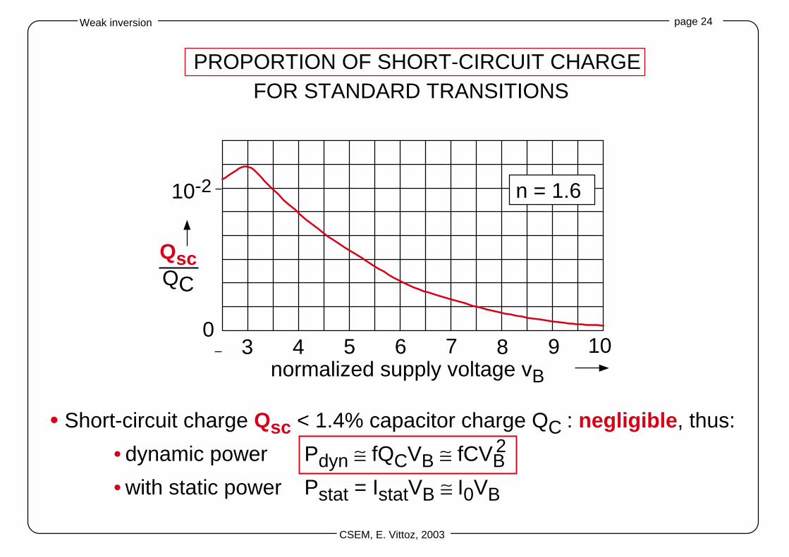
PROPORTION OF SHORT-CIRCUIT CHARGEFOR STANDARD TRANSITIONS
3 100
10-2
4 5 6 7 8 9
QscQC
n = 1.6
normalized supply voltage vB
• Short-circuit charge Qsc < 1.4% capacitor charge QC : negligible, thus:
• dynamic power Pdyn ≅ fQCVB ≅ fCVB
• with static power Pstat = IstatVB ≅ I0VB
2
page 25
CSEM, E. Vittoz, 2003
Weak inversion
0
2
4
6
8
10
2 4 6 8 10 12
PTd CUT
2α=1 0.5
0.20.1
0.050.030.010.003
norm
aliz
edpo
wer
-del
ay p
rodu
ct
n =1.6
normalized supply voltage vB
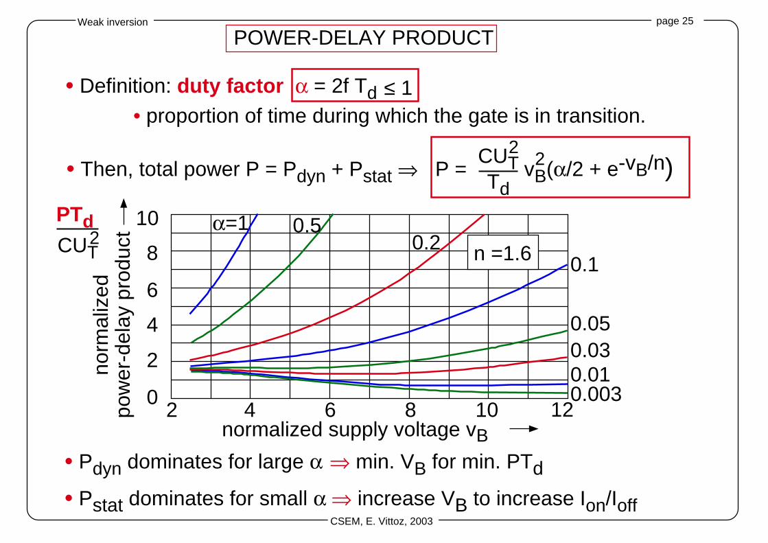
POWER-DELAY PRODUCT
• Definition: duty factor α = 2f Td ≤ 1
• Then, total power P = Pdyn + Pstat ⇒ P = vB(α/2 + e-vB/n) CUTTd
2
• Pdyn dominates for large α ⇒ min. VB for min. PTd
• Pstat dominates for small α ⇒ increase VB to increase Ion/Ioff
• proportion of time during which the gate is in transition.
2
page 26
CSEM, E. Vittoz, 2003
Weak inversion
2 4 6 8 10 12 141
10
100
1000
normalized supply/slope factor vB/n
norm
aliz
ed to
tal p
ower
1
10-210-3 10-4
10-4
10-3
10-2e-3
e-3
Pdyn
Pstat
parameter α
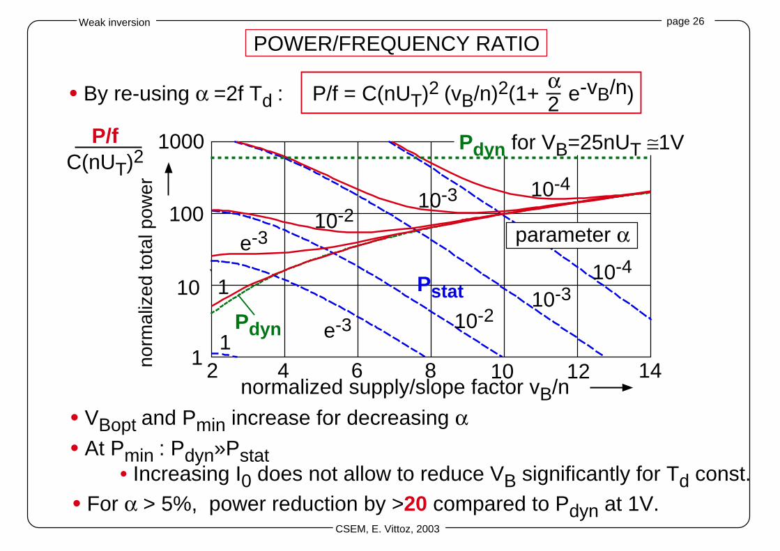
Pdyn for VB=25nUT ≅1VP/fC(nUT)2
POWER/FREQUENCY RATIO
• By re-using α =2f Td : P/f = C(nUT)2 (vB/n)2(1+ e-vB/n) α2
• VBopt and Pmin increase for decreasing α• At Pmin : Pdyn»Pstat
• Increasing I0 does not allow to reduce VB significantly for Td const.
1
• For α > 5%, power reduction by >20 compared to Pdyn at 1V.
page 27
CSEM, E. Vittoz, 2003
Weak inversion
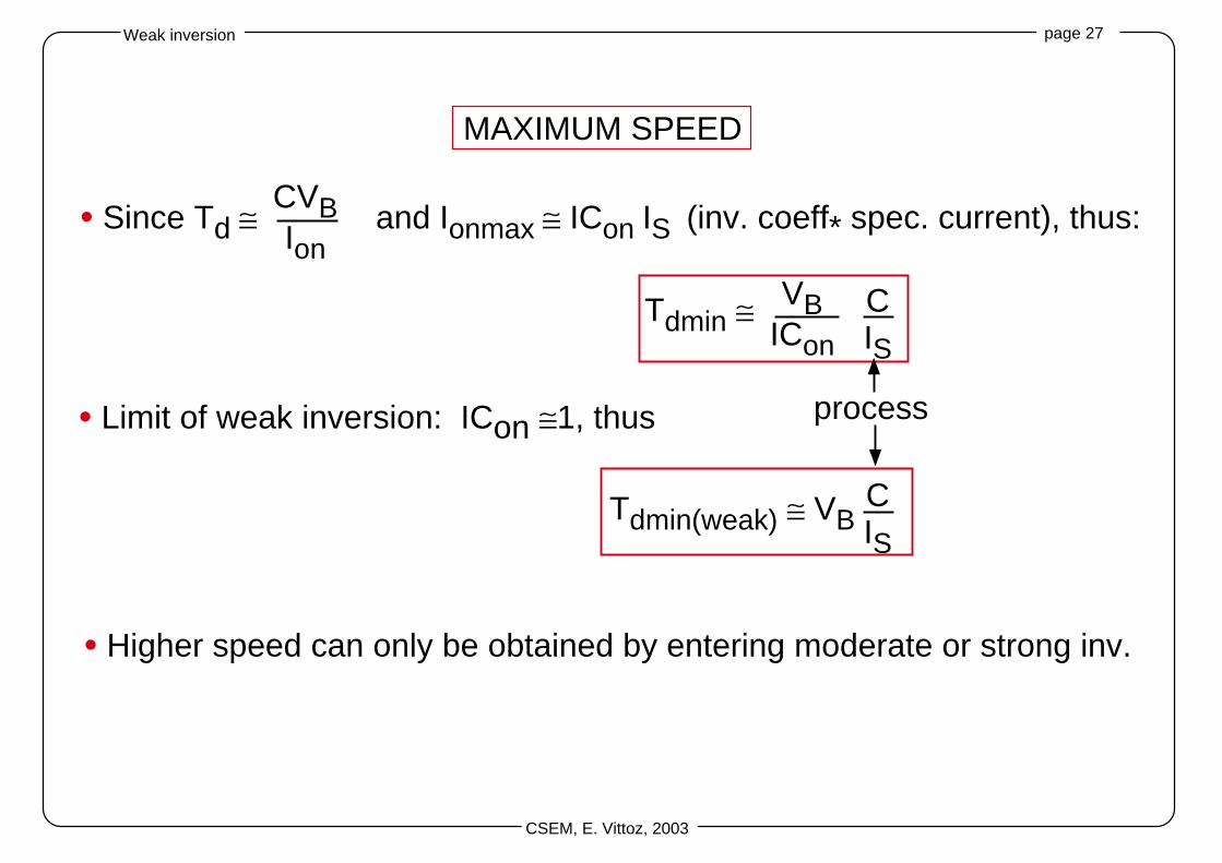
MAXIMUM SPEED
• Since Td ≅ and Ionmax ≅ ICon IS (inv. coeff* spec. current), thus: CVBIon
Tdmin ≅ CIS
VBICon
Tdmin(weak) ≅ VB CIS
process• Limit of weak inversion: ICon ≅1, thus
• Higher speed can only be obtained by entering moderate or strong inv.
page 28
CSEM, E. Vittoz, 2003
Weak inversion
10
103
105
10210110-1 1 1030
20
40
60
"on" inv. coeff. ICon
param.Ion/Ioff
∆VGSnUT
VG
S s
win
g
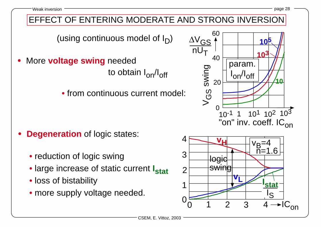
EFFECT OF ENTERING MODERATE AND STRONG INVERSION
• More voltage swing neededto obtain Ion/Ioff
• from continuous current model:
• Degeneration of logic states:
• reduction of logic swing• large increase of static current Istat• loss of bistability• more supply voltage needed.
0 ICon
vH
2 40
1
3
4
3
vL
1
2logicswing
n=1.6vB=4
IstatIS
(using continuous model of ID)
page 29
CSEM, E. Vittoz, 2003
Weak inversion
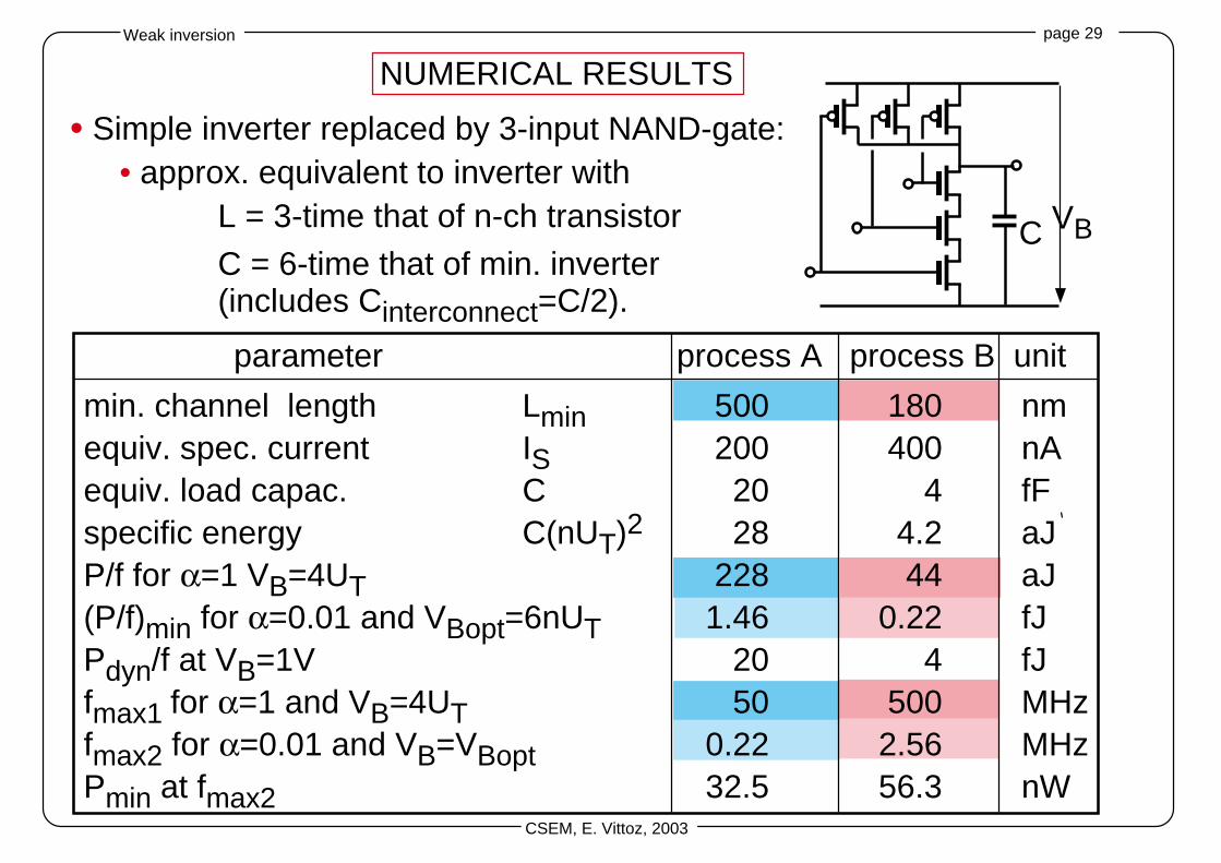
NUMERICAL RESULTS
• Simple inverter replaced by 3-input NAND-gate:• approx. equivalent to inverter with
L = 3-time that of n-ch transistor
C = 6-time that of min. inverter(includes Cinterconnect=C/2).
VBC
parameter process A process B unit
min. channel length Lmin 500 180 nmequiv. spec. current IS 200 400 nAequiv. load capac. C 20 4 fFspecific energy C(nUT)2 28 4.2 aJP/f for α=1 VB=4UT 228 44 aJ(P/f)min for α=0.01 and VBopt=6nUT 1.46 0.22 fJPdyn/f at VB=1V 20 4 fJfmax1 for α=1 and VB=4UT 50 500 MHzfmax2 for α=0.01 and VB=VBopt 0.22 2.56 MHzPmin at fmax2 32.5 56.3 nW
page 30
CSEM, E. Vittoz, 2003
Weak inversion
PRACTICAL CONSIDERATIONS AND LIMITATIONS
• Low-voltage power source• should be proportional to UT (PTAT)• need for power-efficient adapter from higher supply voltage.
• Asymmetry• p/n asymmetry may result in speed reduction.
• Mismatch• dominated by threshold mismatch δVT• may result in speed reduction proportional to δVT /VB.
• Short channel effects: should not drastically degrade the results.
• Gate leakage current : should be alleviated by very low VB.
• Adjustment of I0 orTd to required value
• control by VS with charge pump in loop [18]; n>1 needed (no SOI!)
• corresponds to threshold adjustment unavoidable at very low VB.
• System architectures and applications.
page 31
CSEM, E. Vittoz, 2003
Weak inversion
SYSTEM ARCHITECTURE AND APPLICATIONS
• Duty factor α must be maximized to reach minimum P/f,
(where f is the average transition frequency), thus
• avoid idling gates (contrary to traditional CMOS culture)
• new architectures needed:
- maximally active gates of minimum speed (max. delay time Td)
- particular problem with RAMs (short Td but sparse activity)
- how? new constraints should result in novel solutions.
• partition the system in blocks of comparable α and Td
- optimum VB and I0 for each block (separate I0 control).
• Maximum frequency much lower than for strong inversion:
• best applicable when no high local speed is required
• m-parallelize: mTd but same power if same α (m units with P/m)
- digital image processing ?
page 32
CSEM, E. Vittoz, 2003
Weak inversion
CONCLUSION
• Weak inversion permits very low supply voltage VB
• approached with scaled-down VB: IC ~ VB• limit for scaled-down VB.
• Analog: • VB>10UT = 250 mV• provides maximum gm/ID• bipolar-like behaviour can be exploited in new schemes.
• Digital: • VB> 4UT = 100mV• transistor not a switch but a current modulator (Ion/Ioff)• new architectural approaches for max. duty factor α.• ultimum (asymptotic) limit for low power*delay.
• Low speed, but keeps increasing with 1/L2 in scaled down processes.
2
page 33
CSEM, E. Vittoz, 2003
Weak inversion
[1] E.Vittoz and J.Fellrath, "CMOS analog integrated circuits based on weak inversion operation", IEEE J.Solid-State Circuits, vol.SC-12, pp.224-231, June 1977.
[2] E.Vittoz, "Micropower techniques", in Design of VLSI Circuits for Telecommunications and Signal Processing, J.E.Franca and Y.P.Tsividis Editors, PrenticeHall, 1991
[3]. C.Enz, F.Krummenacher and E.Vittoz, "An analytical MOS transistor model valid in all regions of operation and dedicated to low-voltage and low-currentapplications", Analog Integrated Circuits and Signal Processing, Vol.8, pp.83-114, 1995.
[4] R.M Swanson and J.D.Meindl,"Ion-implanted complementary MOS transistors in low-voltage circuits", IEEE J.Solid-State Circuits, vol.SC-7, pp.146-153, April1972.
[5] E. Vittoz, "Weak inversion for ultimate low-power logic", to be published in Low-Power Electronic Design, ed. C. Piguet, CRC Press LLC (2003?), Chapter 16.
[6] E. Vittoz, C. Enz and F. Krummenacher, "A basic property pf MOS transistors and its circuit implications", Workshop on Compact Modeling, WCMMSM.2003, Febr. 23-27, San F.rancisco, pp. 246-249. Slide of presentation can be downloaded at www.nanotech2003.com/WCM2003.html#Slides.
[7] M.A. Maher and C. Mead, "A physical charge-controlled model for the MOS transistors", Advanced research in VLSI, Proc. of the 1987 Stanford Conference,MIT Press, Cambridge MA, 1987.
[8] A. Cunha et al., "An MOS transistor model for analog circuit design", IEEE J.Solid-State Circuits, vol.33, pp.1510-1519, Oct. 1998.
[9] H. Oguey and S. Cserveny, "MOS modelling at low current density", Summer Course on "Process and Device Modelling", ESAT Leuven-Heverlee, Belgium,June 1983.
[10] H.J.Oguey and D.Aebischer. "CMOS current without resistance."IEEE Journal of Solid-State Circuits, vol 32, pp.1132-1135 July 1997.
[11] K.Bult and G.Geelen, "A inherently linear and compact MOST-only current division technique", Dig. ISSCC Tech. Papers, February 1992, pp.198-199.
[12] E.Vittoz and X.Arreguit,"Linear networks based on transistors", Electronics Letters, vol.29, pp.297-299, 4th Febr. 1993.
[13] E.Vittoz, ÒPseudo-resistive networks and their applications to analog collective computationÓ, Proc. MicroNeuroÕ97, Dresden, pp.163-173.
[14] T. DelbrŸck, "Bump circuit for computing similarity and dissimilarity of analog voltages", Proc. of International Joint Conf. on Neural Networks, vol.1, pp. I -475-479. 1991.
[15] B. Gilbert, "Translinear circuits: a proposed classification", Electron. Letters, vol.11, p.14, 1975.
[16] A. Andreou and K. Boahen, "Neural information processing II" in Analog VLSI Signal and Information Processing, M. Ismail and T. Fiez, editors, pp.358-409,McGraw-Hill, 1994.
[17] E.Vittoz, "Analog VLSI implementation of neural networks", published in the Handbook of Neural Computation, Institute of Physics Publishing and OxfordUniversity Press, USA, 1996.
[18] V. von Kaenel et al. "Automatic adjustment of threshold and supply voltage for minimum power consumption in CMOS digital circuits'', Proc. IEEE Symposiumon Low Power Electronics, San Diego, 1994, pp.78-79.
REFERENCES