Embed Size (px)
Citation preview
AN44
AN44U 1
AN44 DrivingPiezo-electricActuators
1.1INTRODUCTION The word Piezoelectricity is derived from the Greek and
means 'electricity by pressure'. Piezoelectricity is a classical discipline dating back to the research of Jacques and Pierre Curie in the 1880s. The phenomenon, piezoelectricity, describes the interrelationship between mechanical strain upon a solid and its electrical behavior. One can create an electrical output by applying a force to the material sometimes called the direct piezoelectric effect, thereby transforming mechanical energy into electrical energy. Conversely, a distortion can be devel-oped by applying an electric field, the reverse electric effect, which transforms electrical energy into mechanical energy. If the applied voltage is an alternating field, then it will cause the substance to vibrate, thereby generating mechanical waves at the same frequency as the applied field.
From this classical discipline an extraordinary number of applications have been developed, particularly, over the last 20 years. A list, by no means complete, appears in Table 1.
The piezoelectric phenomenon is relatively complex and the reader is referred to the book listed in the 'References' for a more rigorous treatment1. However, in this Application Note we shall confine ourselves to information relating to piezoelectric actuators and to the electronics that is essential to drive them.
1.2PIEZOELECTRICCRYSTALSPiezoelectric actuators are fabricated from materials that
exhibit the piezoelectric effect. These include a number of naturally-occurring crystals such as quartz, tourmaline and sodium potassium tartrate. In addition there are piezoelectric ceramics which include lead titanate and lead zirconate which
are often identified as PZT. These materials exhibit certain advantages over single-crystal quartz including higher piezo-electric coefficients, ease of fabrication into components of any size and shape, mechanically hard and robust, as well as chemically inert. PZT devices are manufactured from their respective oxides and carbonates of Pb, Zr, Ti, rare earths, and alkaline metals.
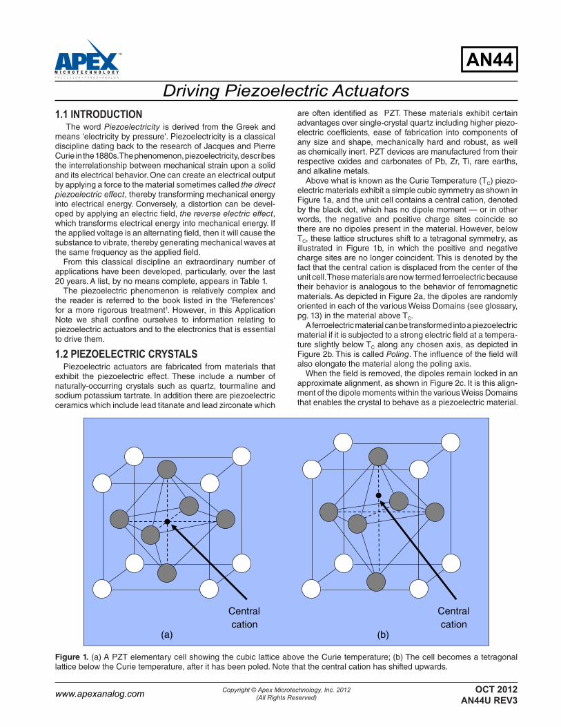
Above what is known as the Curie Temperature (TC) piezo-electric materials exhibit a simple cubic symmetry as shown in Figure 1a, and the unit cell contains a central cation, denoted by the black dot, which has no dipole moment — or in other words, the negative and positive charge sites coincide so there are no dipoles present in the material. However, below TC, these lattice structures shift to a tetragonal symmetry, as illustrated in Figure 1b, in which the positive and negative charge sites are no longer coincident. This is denoted by the fact that the central cation is displaced from the center of the unit cell. These materials are now termed ferroelectric because their behavior is analogous to the behavior of ferromagnetic materials. As depicted in Figure 2a, the dipoles are randomly oriented in each of the various Weiss Domains (see glossary, pg. 13) in the material above TC.
A ferroelectric material can be transformed into a piezoelectric material if it is subjected to a strong electric field at a tempera-ture slightly below TC along any chosen axis, as depicted in Figure 2b. This is called Poling. The influence of the field will also elongate the material along the poling axis.
When the field is removed, the dipoles remain locked in an approximate alignment, as shown in Figure 2c. It is this align-ment of the dipole moments within the various Weiss Domains that enables the crystal to behave as a piezoelectric material.
Centralcation
Centralcation
(a) (b)
Figure 1. (a) A PZT elementary cell showing the cubic lattice above the Curie temperature; (b) The cell becomes a tetragonal lattice below the Curie temperature, after it has been poled. Note that the central cation has shifted upwards.
Driving Piezoelectric Actuators
AN44
Copyright © Apex Microtechnology, Inc. 2012(All Rights Reserved)www.apexanalog.com OCT2012
AN44UREV3
AN44
2 AN44U
+
++
+++
+
+
+
+
+
+
+
+
-
-
-
---
-
-
-
--
-
-
-
+
-
+
-
+
-
+
-
+
-
+
-
+
-
+
-
+
-
+
-
+
-
+
-
+
-
+
-
+
-
+
-
+
-
+
-
+
-
+
-
+
-
+
-
+
-
+
-
+
-
+
-
+
-
+
-
+
-
+
-
+
-
+
-
+
-
+
-
+
-
+
-
+
-
+
-
+
-
+
-
+
-
+
-
+
-
+
-
+
-
+
-
+
-
+
-
+
-
+
-
+
-
+
-
+
-
+
-
+
-
+
-
+
-
+
-
+
-
+
(a) (b) (c)
Polingvoltage
Polingaxis
Weissdomain
Figure 2. How the electric dipole moments align before polarization (a), during polarization (b) and after polarization (c).
Their benefits• No moving parts – makes motion in the sub-nanometer
range possible. Because there are no moving parts in contact, there is virtually no limit on resolution.
• Fast response - piezoelectric actuators respond in a matter of microseconds. Acceleration rates of more than 10,000 g can be realized.
• High force generation - capable of moving loads of several tons. Piezoelectric actuators can cover travel ranges of several 100 µm with resolutions in the sub-nanometer range.
• No magnetic fields - because the piezoelectric effect is related to electric fields, piezoelectric actuators produce no magnetic fields nor are they affected by them. Therefore such devices are especially well suited for applications where magnetic fields cannot be tolerated.
• Low power consumption - static operation, even hold-ing heavy loads for long periods, consumes virtually no power. A piezoelectric actuator behaves very much like an electrical capacitor. When at rest, no heat is gener-ated.
• No wear - no moving parts such as gears or bearings. The displacement is based upon solid-state dynamics and therefore exhibits no wear. Endurance tests have been conducted on piezoelectric actuators that have exhibited no measurable change in performance over several billion cycles.
• Vacuum and clean room compatible - piezoelectric actuators cause no wear nor require lubricants.
• Operates at cryogenic temperatures - the piezoelectric
effect continues to operate even at temperatures ap-proaching zero degrees Kelvin.
TABLE1.PIEZOELECTRICACTUATORS—BENEFITSANDAPPLICATIONS
Their applicationsData Storage • Magnetic recording head testing• Spin stands• Disk testing• Active vibration cancellation• Pole-tip recession test
Semiconductors, Microelectronics • Nano & Microlithography• Ultrasonic soldering• Wafer and mask positioning• Ultrasonic wirebonders• Inspection systems• Active vibration cancellation
Precision Mechanics • Fast tool servos• Ultrasonic drilling• Active vibration cancellation• Structural deformation• Tool adjustment• Wear compensation• Needle-valve actuation
• Micropumps• Linear drives• Knife-edge control in extrusion tools• Micro-engraving systems
Medical and Dental Technologies • Brain scanners• Ultrasonic cataract removal• Ultrasonic scalpels• Plaque scalers• Lithotripters• Cell penetration• Microdispensers
Optics, Photonics • Scanning mirrors• Image stabilization, pixel multiplication• Scanning microscopy• Auto-focus systems• Fiber-optic alignment• Fiber-optic switching• Adaptive and active optics• Laser tuning• Vibration stimulation

AN44
AN44U 3
1.3PIEZOELECTRICSACTUATORS—SOMEBASICSWithin the cylindrical piezoelectric actuator illustrated
in Figure 3a, when a voltage is applied longitudinally, a deformation occurs along the axis of the device causing a displacement ΔL, as depicted in the illustration. Typically a piezoelectric material can withstand a strain, or change in length, of 0.1%. This means that an actuator that is 100-mil-limeters long that is poled (energized) along its axis can be expanded by 0.1 mm.
The displacement, or change in length of an unloaded single-layer piezoelectric actuator can be closely approxi-mated by:
(1)
Where: ΔL = the change in length (meters) S = strain-per-unit length or relative length change
(meters/meter, and therefore, dimensionless) E = the electric field strength (volts/meter) LO = the length of the actuator (meters) d33 = piezoelectric coefficient (meters-per-volt) where
the first subscript identities the axis of the field and the second subscript identifies the axis of the displacement.
The maximum electric field that most ceramic piezoelectric actuators can withstand is on the order of 1 to 2 kV/millimeter. To extend the travel beyond the approximately 0.1% maximum of a single slice and to avoid applying too large an applied field, a multilayer piezoelectric actuator can be fabricated by gluing thin layers of the piezo material together to form a stack. A voltage is then applied to each layer individually, as depicted in Figure 3b, so that each is powered, independently.
Now the applied voltage applied to each slice is still the same, but the total displacement is simply the sum of the individual displacements, or:
(2)
1.4DRIVINGATFREQUENCIESBELOWRESONANCEWhen a piezoelectric actuator is driven by an AC voltage,
the equivalent circuit is quite complex2. However, when a piezoelectric actuator is driven by a periodic voltage source
with a frequency below the resonant frequency of the piezo-electric actuator, which is often the case in inkjet applications, then the device can be modeled by a single capacitor. In this case the impedance presented to the driving source is, to a close approximation, simply:
(3)
Where: f = the frequency of the driving source CPA = the equivalent capacitance of the piezoelectric
actuator
2.1GUIDELINESFORDESIGNINGDRIVERCIRCUITS Some essentials to keep in mind when designing systems
that employ piezoelectric actuators are these: • Limited strength in tension - The tensile strength of a
cylindrical piezoelectric actuator is approximately 10% of its strength in compression. It is essential to abide by these values to avoid fracturing the piezoelectric actuator. Specific values can be obtained from data sheets supplied by piezoelectric actuator manufacturers.
• Boundaries on acceleration - When driven by a periodic waveform the acceleration will increase exponentially with frequency. So it is important to identify the upper limit of the device's ability to withstand high acceleration forces. In particular, multilayer piezoelectric actuators are vulnerable to delamination should their acceleration limits be exceeded.
• Driver circuits do consume power - Piezoelectric actuators consume virtually no power when static, other than the quiescent power consumed by the electronics. However, the power dissipation demands upon the operational power amplifier circuits when the actuator is driven are significant, indeed.
• Follow sound principles in designing the driving circuits – Make sure the driving power operational amplifiers are operating in their safe operating region and current limit-ing is provided to protect the circuitry from an inadvertent short circuit. Other essential design tasks include selecting a satisfactory heatsink, flyback diodes and compensation capacitors. Many of these issues are covered in the dis-cussion of the sample circuits described in the following sections.
∆L = SLO ≈ Ed33LO
∆LTOT = N∆L
ZLOAD =1
2πfCPA
∆LV
+
–
∆L
V+L
(a) (b)
Figure 3. Two Linear Piezoelectric Actuators — A single stack in (a) and a multilayer (b) in which the displacement is amplified by the number of slices.
AN44
4 AN44U
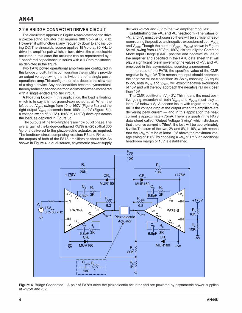
2.2ABRIDGE-CONNECTEDDRIVERCIRCUITThe circuit that appears in Figure 4 was developed to drive
a piezoelectric actuator that requires 300 Vp-p at 80 kHz. However, it will function at any frequency down to and includ-ing DC. The sinusoidal source applies 15 Vp-p at 80 kHz to drive the amplifier pair which, in turn, drives the piezoelectric actuator. In this case the actuator can be represented by a 1-nanofarad capacitance in series with a 1-Ohm resistance, as depicted in the figure.
Two PA78 power operational amplifiers are configured in this bridge circuit3. In this configuration the amplifiers provide an output voltage swing that is twice that of a single power operational amp. This configuration also doubles the slew rate of a single device. Any nonlinearities become symmetrical, thereby reducing second-harmonic distortion when compared with a single-ended amplifier circuit.
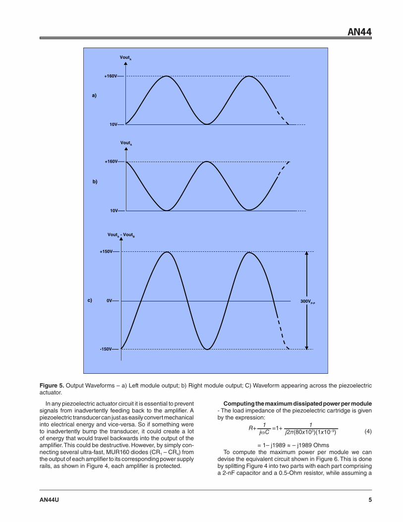
A Floating Load - In this application, the load is floating, which is to say it is not ground-connected at all. When the left output VOUTA swings from 10 to 160V (Figure 5a) and the right output VOUTB descends from 160V to 10V (Figure 5b), a voltage swing of 300V (-150V to +150V) develops across the load, as depicted in Figure 5c.
The outputs of the two amplifiers are now out of phase. The overall gain of the bridge-configured PA78s is +20 so that 300 Vp-p is delivered to the piezoelectric actuator, as required. The feedback circuit comprising resistors R3 and R4 center the outputs of both of the PA78 amplifiers at about 85V. As shown in Figure 4, a dual-source, asymmetric power supply
delivers +175V and -5V to the two amplifier modules4.Establishing the +VS and -VS headroom - The values of
+VS and -VS must be chosen so there will be sufficient head-room during the positive and negative excursions of both VOUTA and VOUTB. Though the output (VOUTA – VOUTB) shown in Figure 5c, will swing from +150V to -150V, it is actually the Common Mode Input Range (CMR) positive and negative values of the amplifier and specified in the PA78 data sheet that will play a significant role in governing the values of +VS and -VS employed in this asymmetrical sourcing arrangement.
In the case of the PA78, the specified value of the CMR negative is -VS + 3V. This means the input should approach the negative rail no closer than 3V. So by choosing -VS equal to -5V, both VOUTA and VOUTB, will exhibit negative excursions of 10V and will thereby approach the negative rail no closer than 15V.
The CMR positive is +VS - 2V. This means the most posi-tive-going excursion of both VOUTA and VOUTB must stay at least 2V below +VS. A second issue with regard to the +VS rail is the voltage drop at the output when the amplifiers are delivering peak current — and in this application the peak current is approximately 75mA. There is a graph in the PA78 data sheet called "Output Voltage Swing" which discloses that the drive current is 75mA, the loss will be approximately 8 volts. The sum of the two, 2V and 8V, is 10V, which means that the +VS must be at least 10V above the maximum volt-age swing of 150V. By choosing a +VS of 175V an additional headroom margin of 15V is established.
+V1
15VP-P
0 to 80 kHz
RF
20K
RC
3KRLIMA
8.2
RF
10K
RC
3KRLIMB
6.8
RINB
10K
RB
3K
RB
3K
RLOAD
1
R5
10K
R6
10K
R4
20K
R3
1K
CB
6.8pF
CB
6.8pF
CC
6.8pF
CC
6.8pF
CLOAD
1nF
CR1
MUR160
CR3
MUR160
CR4
MUR160
CR2
MUR160
+175V +175V
+175V
–5V
–5V
–5V
PiezoelectricActuator
VOUTACC+
CR+–VS
ILIM
CR–
CC
+VS
+IN
–IN
PA78-AVOUTB CC+
CR+
–VS
ILIM
CR–
CC
+VS
+IN
–IN
PA78-B
Figure 4. Bridge Connected – A pair of PA78s drive the piezoelectric actuator and are powered by asymmetric power supplies at +175V and -5V.
AN44
AN44U 5
In any piezoelectric actuator circuit it is essential to prevent signals from inadvertently feeding back to the amplifier. A piezoelectric transducer can just as easily convert mechanical into electrical energy and vice-versa. So if something were to inadvertently bump the transducer, it could create a lot of energy that would travel backwards into the output of the amplifier. This could be destructive. However, by simply con-necting several ultra-fast, MUR160 diodes (CR1 – CR4) from the output of each amplifier to its corresponding power supply rails, as shown in Figure 4, each amplifier is protected.
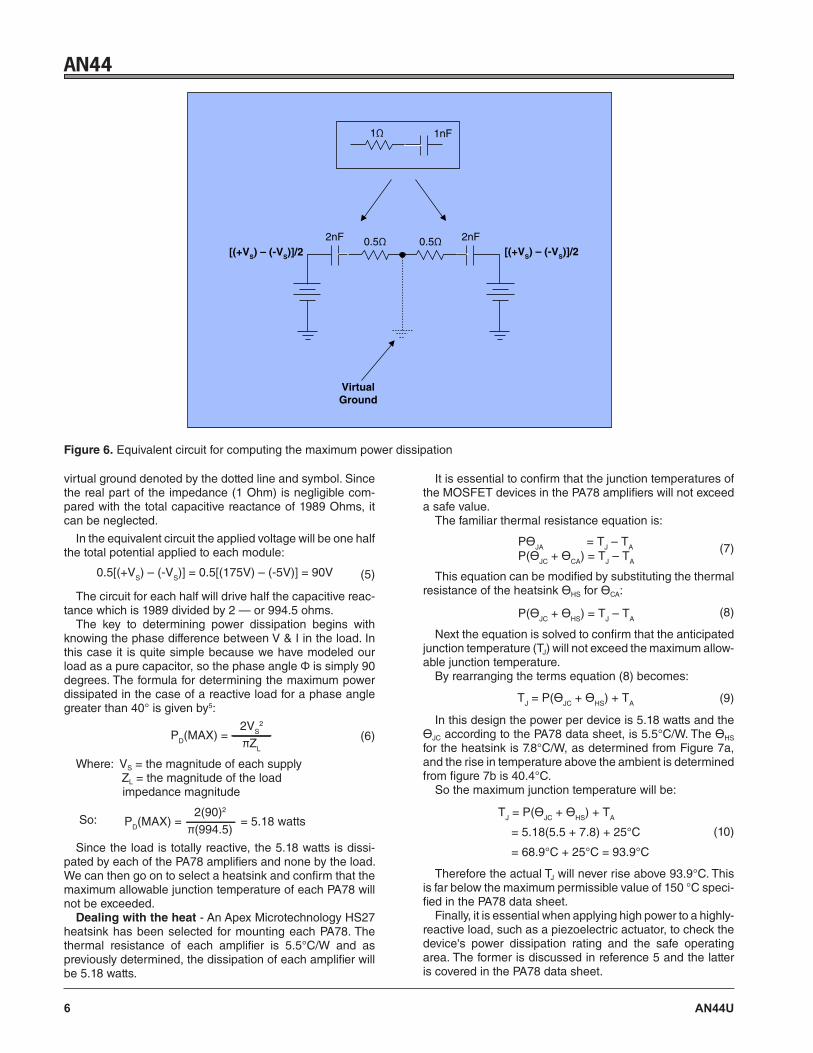
Computing the maximum dissipated power per module - The load impedance of the piezoelectric cartridge is given by the expression:
(4)
To compute the maximum power per module we can devise the equivalent circuit shown in Figure 6. This is done by splitting Figure 4 into two parts with each part comprising a 2-nF capacitor and a 0.5-Ohm resistor, while assuming a
VoutA
a)
+160V–—
10V–—
VoutA
b)
+160V–—
10V–—
VoutA - VoutB
c)
+150V–—
0V–—
-150V–—
300VP-P
Figure 5. Output Waveforms – a) Left module output; b) Right module output; C) Waveform appearing across the piezoelectric actuator.
1j2π(80x103)(1x10⁻⁹)
1jωC
R+ =1+
= 1– j1989 ≈ – j1989 Ohms
AN44
6 AN44U
It is essential to confirm that the junction temperatures of the MOSFET devices in the PA78 amplifiers will not exceed a safe value.
The familiar thermal resistance equation is:
(7)
This equation can be modified by substituting the thermal resistance of the heatsink ѲHS for ѲCA:
(8)
Next the equation is solved to confirm that the anticipated junction temperature (TJ) will not exceed the maximum allow-able junction temperature.
By rearranging the terms equation (8) becomes:
(9)
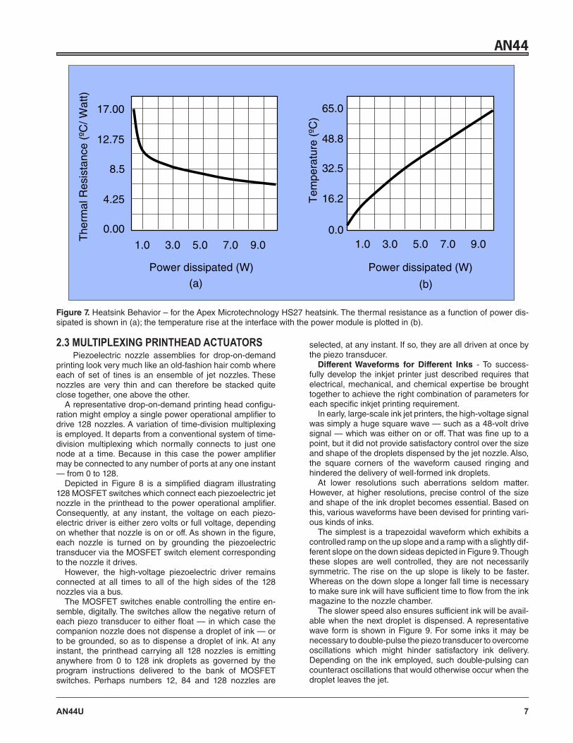
In this design the power per device is 5.18 watts and the ѲJC according to the PA78 data sheet, is 5.5°C/W. The ѲHS for the heatsink is 7.8°C/W, as determined from Figure 7a, and the rise in temperature above the ambient is determined from figure 7b is 40.4°C.
So the maximum junction temperature will be:
(10)
Therefore the actual TJ will never rise above 93.9°C. This is far below the maximum permissible value of 150 °C speci-fied in the PA78 data sheet.
Finally, it is essential when applying high power to a highly-reactive load, such as a piezoelectric actuator, to check the device's power dissipation rating and the safe operating area. The former is discussed in reference 5 and the latter is covered in the PA78 data sheet.
virtual ground denoted by the dotted line and symbol. Since the real part of the impedance (1 Ohm) is negligible com-pared with the total capacitive reactance of 1989 Ohms, it can be neglected.
In the equivalent circuit the applied voltage will be one half the total potential applied to each module:
(5)
The circuit for each half will drive half the capacitive reac-tance which is 1989 divided by 2 — or 994.5 ohms.
The key to determining power dissipation begins with knowing the phase difference between V & I in the load. In this case it is quite simple because we have modeled our load as a pure capacitor, so the phase angle Ф is simply 90 degrees. The formula for determining the maximum power dissipated in the case of a reactive load for a phase angle greater than 40° is given by5:
(6)
Where: VS = the magnitude of each supply ZL = the magnitude of the load impedance magnitude
So: Since the load is totally reactive, the 5.18 watts is dissi-
pated by each of the PA78 amplifiers and none by the load. We can then go on to select a heatsink and confirm that the maximum allowable junction temperature of each PA78 will not be exceeded.
Dealing with the heat - An Apex Microtechnology HS27 heatsink has been selected for mounting each PA78. The thermal resistance of each amplifier is 5.5°C/W and as previously determined, the dissipation of each amplifier will be 5.18 watts.
0.5[(+VS) – (-VS)] = 0.5[(175V) – (-5V)] = 90V
PD(MAX) =2VS
2
πZL
PD(MAX) =2(90)2
π(994.5)= 5.18 watts
PѲJA = TJ – TA
P(ѲJC + ѲCA) = TJ – TA
P(ѲJC + ѲHS) = TJ – TA
TJ = P(ѲJC + ѲHS) + TA
TJ = P(ѲJC + ѲHS) + TA
= 5.18(5.5 + 7.8) + 25°C
= 68.9°C + 25°C = 93.9°C
1Ω 1nF
0.5Ω 0.5Ω2nF 2nF[(+VS) – (-VS)]/2[(+VS) – (-VS)]/2
VirtualGround
Figure 6. Equivalent circuit for computing the maximum power dissipation
AN44
AN44U 7
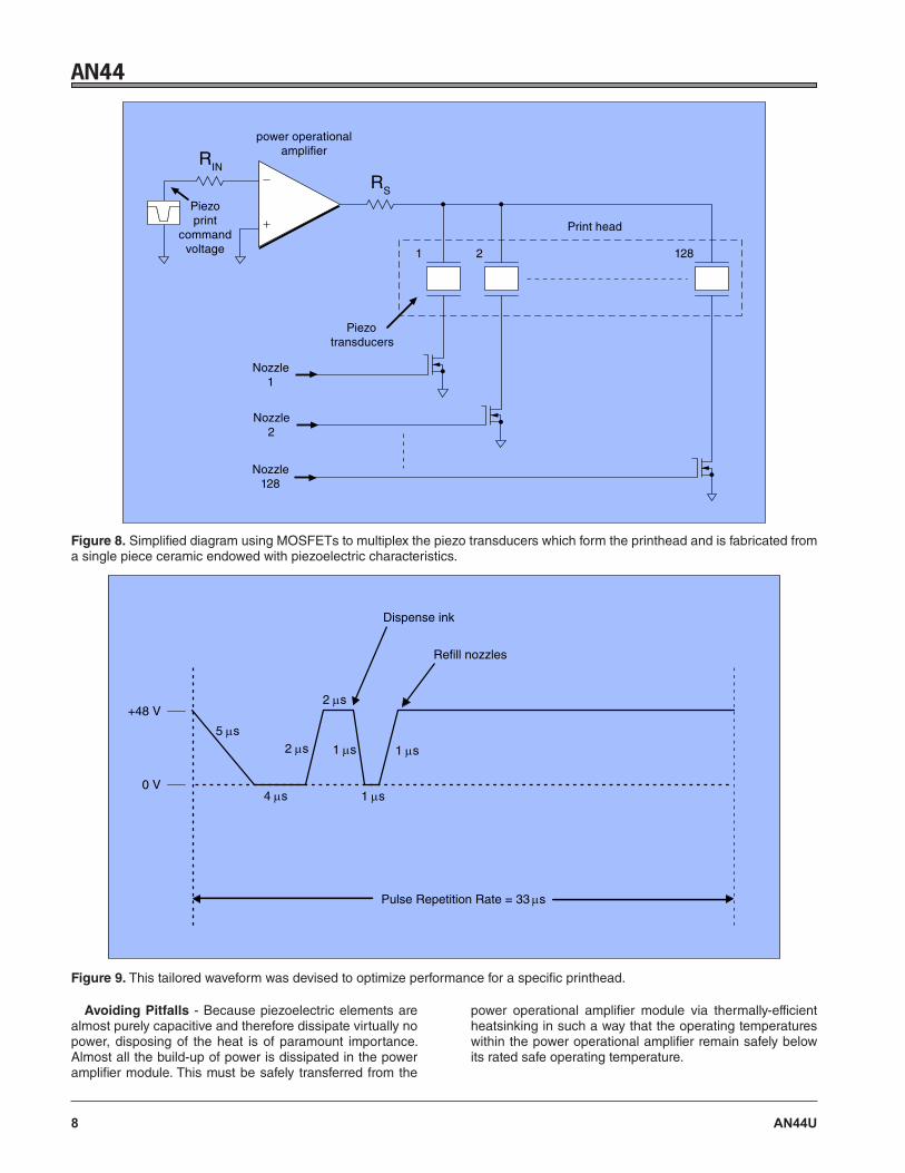
selected, at any instant. If so, they are all driven at once by the piezo transducer.
Different Waveforms for Different Inks - To success-fully develop the inkjet printer just described requires that electrical, mechanical, and chemical expertise be brought together to achieve the right combination of parameters for each specific inkjet printing requirement.
In early, large-scale ink jet printers, the high-voltage signal was simply a huge square wave — such as a 48-volt drive signal — which was either on or off. That was fine up to a point, but it did not provide satisfactory control over the size and shape of the droplets dispensed by the jet nozzle. Also, the square corners of the waveform caused ringing and hindered the delivery of well-formed ink droplets.
At lower resolutions such aberrations seldom matter. However, at higher resolutions, precise control of the size and shape of the ink droplet becomes essential. Based on this, various waveforms have been devised for printing vari-ous kinds of inks.
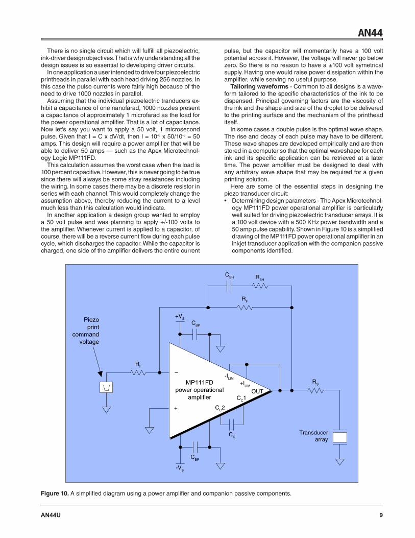
The simplest is a trapezoidal waveform which exhibits a controlled ramp on the up slope and a ramp with a slightly dif-ferent slope on the down sideas depicted in Figure 9. Though these slopes are well controlled, they are not necessarily symmetric. The rise on the up slope is likely to be faster. Whereas on the down slope a longer fall time is necessary to make sure ink will have sufficient time to flow from the ink magazine to the nozzle chamber.
The slower speed also ensures sufficient ink will be avail-able when the next droplet is dispensed. A representative wave form is shown in Figure 9. For some inks it may be necessary to double-pulse the piezo transducer to overcome oscillations which might hinder satisfactory ink delivery. Depending on the ink employed, such double-pulsing can counteract oscillations that would otherwise occur when the droplet leaves the jet.
2.3MULTIPLEXINGPRINTHEADACTUATORS Piezoelectric nozzle assemblies for drop-on-demand
printing look very much like an old-fashion hair comb where each of set of tines is an ensemble of jet nozzles. These nozzles are very thin and can therefore be stacked quite close together, one above the other.
A representative drop-on-demand printing head configu-ration might employ a single power operational amplifier to drive 128 nozzles. A variation of time-division multiplexing is employed. It departs from a conventional system of time-division multiplexing which normally connects to just one node at a time. Because in this case the power amplifier may be connected to any number of ports at any one instant — from 0 to 128.
Depicted in Figure 8 is a simplified diagram illustrating 128 MOSFET switches which connect each piezoelectric jet nozzle in the printhead to the power operational amplifier. Consequently, at any instant, the voltage on each piezo-electric driver is either zero volts or full voltage, depending on whether that nozzle is on or off. As shown in the figure, each nozzle is turned on by grounding the piezoelectric transducer via the MOSFET switch element corresponding to the nozzle it drives.
However, the high-voltage piezoelectric driver remains connected at all times to all of the high sides of the 128 nozzles via a bus.
The MOSFET switches enable controlling the entire en-semble, digitally. The switches allow the negative return of each piezo transducer to either float — in which case the companion nozzle does not dispense a droplet of ink — or to be grounded, so as to dispense a droplet of ink. At any instant, the printhead carrying all 128 nozzles is emitting anywhere from 0 to 128 ink droplets as governed by the program instructions delivered to the bank of MOSFET switches. Perhaps numbers 12, 84 and 128 nozzles are
1.0 3.0 5.0 7.0 9.0 1.0 3.0 5.0 7.0 9.0
17.00
12.75
8.5
4.25
0.00
65.0
48.8
32.5
16.2
0.0
Power dissipated (W) Power dissipated (W)
The
rmal
Res
ista
nce
(ºC
/ Wat
t)
Tem
pera
ture
(ºC
)
(a) (b)
Figure 7. Heatsink Behavior – for the Apex Microtechnology HS27 heatsink. The thermal resistance as a function of power dis-sipated is shown in (a); the temperature rise at the interface with the power module is plotted in (b).
AN44
8 AN44U
1 µs
2 µs
0 V
+48 V
Pulse Repetition Rate = 33 µs
1 µs
1 µs
2 µs
4 µs
5 µs
Dispense ink
Refill nozzles
Figure 9. This tailored waveform was devised to optimize performance for a specific printhead.
RS
power operationalamplifier
Piezotransducers
1 2 128
Piezoprint
commandvoltage
Nozzle1
Nozzle128
Nozzle2
Print head
RIN
Figure 8. Simplified diagram using MOSFETs to multiplex the piezo transducers which form the printhead and is fabricated from a single piece ceramic endowed with piezoelectric characteristics.
Avoiding Pitfalls - Because piezoelectric elements are almost purely capacitive and therefore dissipate virtually no power, disposing of the heat is of paramount importance. Almost all the build-up of power is dissipated in the power amplifier module. This must be safely transferred from the
power operational amplifier module via thermally-efficient heatsinking in such a way that the operating temperatures within the power operational amplifier remain safely below its rated safe operating temperature.
AN44
AN44U 9
There is no single circuit which will fulfill all piezoelectric, ink-driver design objectives. That is why understanding all the design issues is so essential to developing driver circuits.
In one application a user intended to drive four piezoelectric printheads in parallel with each head driving 256 nozzles. In this case the pulse currents were fairly high because of the need to drive 1000 nozzles in parallel.
Assuming that the individual piezoelectric tranducers ex-hibit a capacitance of one nanofarad, 1000 nozzles present a capacitance of approximately 1 microfarad as the load for the power operational amplifier. That is a lot of capacitance. Now let's say you want to apply a 50 volt, 1 microsecond pulse. Given that I = C x dV/dt, then I = 10-6 x 50/10-6 = 50 amps. This design will require a power amplifier that will be able to deliver 50 amps — such as the Apex Microtechnol-ogy Logic MP111FD.
This calculation assumes the worst case when the load is 100 percent capacitive. However, this is never going to be true since there will always be some stray resistances including the wiring. In some cases there may be a discrete resistor in series with each channel. This would completely change the assumption above, thereby reducing the current to a level much less than this calculation would indicate.
In another application a design group wanted to employ a 50 volt pulse and was planning to apply +/-100 volts to the amplifier. Whenever current is applied to a capacitor, of course, there will be a reverse current flow during each pulse cycle, which discharges the capacitor. While the capacitor is charged, one side of the amplifier delivers the entire current
pulse, but the capacitor will momentarily have a 100 volt potential across it. However, the voltage will never go below zero. So there is no reason to have a ±100 volt symetrical supply. Having one would raise power dissipation within the amplifier, while serving no useful purpose.
Tailoring waveforms - Common to all designs is a wave-form tailored to the specific characteristics of the ink to be dispensed. Principal governing factors are the viscosity of the ink and the shape and size of the droplet to be delivered to the printing surface and the mechanism of the printhead itself.
In some cases a double pulse is the optimal wave shape. The rise and decay of each pulse may have to be different. These wave shapes are developed empirically and are then stored in a computer so that the optimal waveshape for each ink and its specific application can be retrieved at a later time. The power amplifier must be designed to deal with any arbitrary wave shape that may be required for a given printing solution.
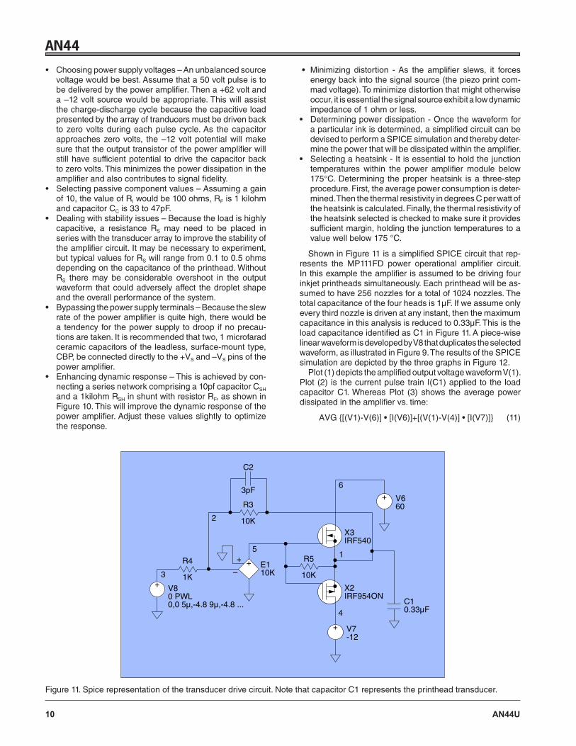
Here are some of the essential steps in designing the piezo transducer circuit:• Determining design parameters - The Apex Microtechnol-
ogy MP111FD power operational amplifier is particularly well suited for driving piezoelectric transducer arrays. It is a 100 volt device with a 500 KHz power bandwidth and a 50 amp pulse capability. Shown in Figure 10 is a simplified drawing of the MP111FD power operational amplifier in an inkjet transducer application with the companion passive components identified.
RSH
RF
RI
RSMP111FDpower operational
amplifier
Piezoprint
commandvoltage
Transducerarray
-ILIM
+
–
CC1OUT
+ILIM
CC2
CSH
CBP
CC
CBP
-VS
+VS
Figure 10. A simplified diagram using a power amplifier and companion passive components.
AN44
10 AN44U
• Minimizing distortion - As the amplifier slews, it forces energy back into the signal source (the piezo print com-mad voltage). To minimize distortion that might otherwise occur, it is essential the signal source exhibit a low dynamic impedance of 1 ohm or less.
• Determining power dissipation - Once the waveform for a particular ink is determined, a simplified circuit can be devised to perform a SPICE simulation and thereby deter-mine the power that will be dissipated within the amplifier.
• Selecting a heatsink - It is essential to hold the junction temperatures within the power amplifier module below 175°C. Determining the proper heatsink is a three-step procedure. First, the average power consumption is deter-mined. Then the thermal resistivity in degrees C per watt of the heatsink is calculated. Finally, the thermal resistivity of the heatsink selected is checked to make sure it provides sufficient margin, holding the junction temperatures to a value well below 175 °C.
Shown in Figure 11 is a simplified SPICE circuit that rep-resents the MP111FD power operational amplifier circuit. In this example the amplifier is assumed to be driving four inkjet printheads simultaneously. Each printhead will be as-sumed to have 256 nozzles for a total of 1024 nozzles. The total capacitance of the four heads is 1µF. If we assume only every third nozzle is driven at any instant, then the maximum capacitance in this analysis is reduced to 0.33µF. This is the load capacitance identified as C1 in Figure 11. A piece-wise linear waveform is developed by V8 that duplicates the selected waveform, as illustrated in Figure 9. The results of the SPICE simulation are depicted by the three graphs in Figure 12.
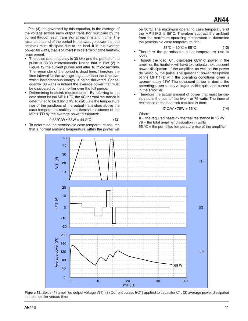
Plot (1) depicts the amplified output voltage waveform V(1). Plot (2) is the current pulse train I(C1) applied to the load capacitor C1. Whereas Plot (3) shows the average power dissipated in the amplifier vs. time:
(11)AVG {[(V1)-V(6)] • [I(V6)]+[(V(1)-V(4)] • [I(V7)]}
Figure 11. Spice representation of the transducer drive circuit. Note that capacitor C1 represents the printhead transducer.
+
++
–
+
+
C2
3pF
R4
1K
R3
10K
R5
10K
C10.33µF
X2IRF954ON
V7-12
X3IRF540
E110K
V660
V80 PWL0,0 5µ,-4.8 9µ,-4.8 ...
1
4
3
5
2
6
• Choosing power supply voltages – An unbalanced source voltage would be best. Assume that a 50 volt pulse is to be delivered by the power amplifier. Then a +62 volt and a –12 volt source would be appropriate. This will assist the charge-discharge cycle because the capacitive load presented by the array of tranducers must be driven back to zero volts during each pulse cycle. As the capacitor approaches zero volts, the –12 volt potential will make sure that the output transistor of the power amplifier will still have sufficient potential to drive the capacitor back to zero volts. This minimizes the power dissipation in the amplifier and also contributes to signal fidelity.
• Selecting passive component values – Assuming a gain of 10, the value of RI would be 100 ohms, RF is 1 kilohm and capacitor CC is 33 to 47pF.
• Dealing with stability issues – Because the load is highly capacitive, a resistance RS may need to be placed in series with the transducer array to improve the stability of the amplifier circuit. It may be necessary to experiment, but typical values for RS will range from 0.1 to 0.5 ohms depending on the capacitance of the printhead. Without RS there may be considerable overshoot in the output waveform that could adversely affect the droplet shape and the overall performance of the system.
• Bypassing the power supply terminals – Because the slew rate of the power amplifier is quite high, there would be a tendency for the power supply to droop if no precau-tions are taken. It is recommended that two, 1 microfarad ceramic capacitors of the leadless, surface-mount type, CBP, be connected directly to the +VS and –VS pins of the power amplifier.
• Enhancing dynamic response – This is achieved by con-necting a series network comprising a 10pf capacitor CSH and a 1kilohm RSH in shunt with resistor RF, as shown in Figure 10. This will improve the dynamic response of the power amplifier. Adjust these values slightly to optimize the response.
AN44
AN44U 11
Plot (3), as governed by this equation, is the average of the voltage across each output transistor multiplied by the current through each transistor at each instant in time. The result at the end of the period is the average power that the heatsink must dissipate due to the load. It is this average power, 68 watts, that is of interest in determining the heatsink requirement. • The pulse rate frequency is 30 kHz and the period of the
pulse is 33.33 microseconds. Notice that in Plot (2) in Figure 12 the current pulses end after 16 microseconds. The remainder of the period is dead time. Therefore the time interval for the average is greater than the time over which instantaneous energy is being delivered. Conse-quently, 68 watts is indeed the average power that must be dissipated by the amplifier over the full period.
• Determining heatsink requirements - By referring to the data sheet for the MP111FD, the AC thermal resistance is determined to be 0.65°C /W. To calculate the temperature rise of the junctions of the output transistors above the case temperature multiply the thermal resistance of the MP111FD by the average power dissipated:
(12)• To determine the permissible case temperature assume
that a normal ambient temperature within the printer will
be 30°C. The maximum operating case temperature of the MP111FD is 85°C. Therefore subtract the ambient from the maximum operating temperature to determine the permissible case temperature rise:
(13)• Therefore the permissible case temperature rise is
55°C.• Though the load, C1, dissipates 68W of power in the
amplifier, the heatsink will have to dissipate the quiescent power dissipation of the amplifier, as well as the power delivered by the pulse. The quiescent power dissipation of the MP111FD with the operating conditions given is approximately 11W. The quiescent power is due to the operating power supply voltages and the quiescent current in the amplifier.
• Therefore the actual amount of power that must be dis-sipated is the sum of the two – or 79 watts. The thermal resistance of the heatsink required is then:
(14)
Where: X = the required heatsink thermal resistance in °C /W 79 = the total amplifier dissipation in watts 55 °C = the permitted temperature rise of the amplifier
0 10 20 30 40Time (µs)
Ave
rage
pow
er (
W)
I(C
1) (
A)
V(1
) (V
)
0
68 W
(1)
(2)
(3)
10
20
30
40
50
-20
-10
0
10
20
0
40
80
120
160
200
Figure 12. Spice (1) amplified output voltage V(1), (2) Current pulses I(C1) applied to capacitor C1, (3) average power dissipated in the amplifier versus time.
0.65°C/W • 68W = 44.2°C
85°C – 30°C = 55°C
X°C/W • 79W = 55°C
AN44
12 AN44U
REFERENCES1. "Piezoelectric Transducers and Applications," Antonio Arnau,
Editor, Springer-Verlag, 20042. "Piezoceramic Properties & Applications," Chapter 2,
Physical Basics, paragraph 2.9, www.morganelectroc-eramics.com
3. Apex Microtechnology, Application Note 20 – Bridge Mode Operation of Power Operational Amplifiers, www.apexanalog.com
4. Apex Microtechnology, Application Note 21, Section 3.1 – Single Supply Operation of Power Operational Amplifiers, www.apexanalog.com
5. Apex Microtechnology, Application Note 1, Section 7.2 – General Operating Considerations, www.apexanalog.com
• Solving equation 14 for X yields a thermal resistance of 0.696 °C/W. Therefore, any heatsink that exhibits a thermal resistance of 0.696 °C/W or less will be acceptable in this application.
• Confirming the maximum junction temperature - Although a maximum junction temperature of 175°C is allowed, for long-term reliability a lower temperature would be better. Check that a heatsink with a thermal resistance of 0.696 °C/W will hold the junction temperature of the output transistors below 175°C:
• As previously mentioned, the 68 watts of power dissipation due to the load causes a temperature rise of 44.2°C in the output transistors. The total junction temperature with the selected heatsink is then the sum of the maximum case temperature and the temperature rise in the output transistors:
(15)
Where: 85°C = the case temperature with the selected heatsink 44.2°C = the temperature rise of the output transistors
due to the load.
• Since a junction temperature of 175°C is allowed, there will be a margin of 45.8°C – acceptable for the heatsink in this application.
• If the power module is to be located near the printhead and the ink is heated, the operating ambient will be well above room temperature of the traditional 25°C. In this case liquid cooling or forced air may be required.
• Note that for illustration purposes the quiescent current in the output stage and some other fine details have been neglected. However, Apex Microtechnology has an online Power Design spread sheet software tool which can easily help you with all the details of arriving at a heatsink thermal resistance for your particular application. Log on to www.apexanalog.com and look for "Circuit Design Software" under the "Support" icon.
Conclusions - As we have shown, devising a driver circuit for inkjet circuits requires tailoring a waveform that will optimize the delivery of the ink droplets by a particular printhead. Then by following the sequence of steps described, the designer will be able to configure a driver circuit that will provide the necessary current pulse train and preserve the fidelity of the waveform delivered to the printhead, while addressing the resulting thermal issues.
85°C + 44.2°C = 129.2°C GLOSSARYCation – An atom or a group of atoms carrying a positive
charge. The charge results because there are more protons than electrons in the cation.
Curie Temperature – The Curie temperature (TC) is the temperature below which a ferroelectric material can be transformed into a piezoelectric material. In the disordered state above the Curie temperature, thermal energy overrides any interactions between the local moments of ions. However, below the Curie temperature, these interactions are predominant and enable the electric dipole moments to align so that the piezoelectric transformation occurs.
Ferroelectric materials – So called because their behavior is analogous to the behavior of ferromagnetic materials.
Poling – The transformation of a ferroelectric material into the piezoelectric state by applying a strong electric field along a chosen axis at a temperature slightly below the Curie temperature (TC). The material will also become elongated along the axis of the field.
Weiss Domains – Regions in a ferroelectric material, with spans on the order of 0.1 to several mm, in which the electric-dipole moments, upon being poled, align so they all face in the same direction.

AN44
AN44U 13
NEEDTECHNICALHELP?CONTACTAPEXSUPPORT!ForallApexMicrotechnologyproductquestionsandinquiries,calltollfree800-546-2739inNorthAmerica.Forinquiriesviaemail,pleasecontactapex.support@apexanalog.com.InternationalcustomerscanalsorequestsupportbycontactingtheirlocalApexMicrotechnologySalesRepresentative.Tofindtheonenearesttoyou,gotowww.apexanalog.comIMPORTANTNOTICE
ApexMicrotechnology,Inc.hasmadeeveryefforttoinsuretheaccuracyofthecontentcontainedinthisdocument.However,theinformationissubjecttochangewithoutnoticeandisprovided"ASIS"withoutwarrantyofanykind(expressedorimplied).ApexMicrotechnologyreservestherighttomakechangeswithoutfurthernoticetoanyspecificationsorproductsmentionedhereintoimprovereliability.ThisdocumentisthepropertyofApexMicrotechnologyandbyfurnishingthisinforma-tion,ApexMicrotechnologygrantsnolicense,expressedorimpliedunderanypatents,maskworkrights,copyrights,trademarks,tradesecretsorotherintellectualpropertyrights.ApexMicrotechnologyownsthecopyrightsassociatedwiththeinformationcontainedhereinandgivesconsentforcopiestobemadeoftheinforma-tiononlyforusewithinyourorganizationwithrespecttoApexMicrotechnologyintegratedcircuitsorotherproductsofApexMicrotechnology.Thisconsentdoesnotextendtoothercopyingsuchascopyingforgeneraldistribution,advertisingorpromotionalpurposes,orforcreatinganyworkforresale.
APEXMICROTECHNOLOGYPRODUCTSARENOTDESIGNED,AUTHORIZEDORWARRANTEDTOBESUITABLEFORUSEINPRODUCTSUSEDFORLIFESUPPORT,AUTOMOTIVESAFETY,SECURITYDEVICES,OROTHERCRITICALAPPLICATIONS.PRODUCTSINSUCHAPPLICATIONSAREUNDER-STOODTOBEFULLYATTHECUSTOMERORTHECUSTOMER’SRISK.
ApexMicrotechnology,ApexandApexPrecisionPoweraretrademarksofApexMicrotechnolgy,Inc.Allothercorporatenamesnotedhereinmaybetrademarksoftheirrespectiveholders.
Copyright © Apex Microtechnology, Inc. 2012(All Rights Reserved)www.apexanalog.com OCT2012
AN44UREV3


![[DESIGN] Piezo-Piezo to Pie](https://img.pdfslide.us/doc/110x75/5571f8bb49795991698df909/design-piezo-piezo-to-pie.jpg)