Embed Size (px)
Citation preview

iSim™ ISL6742 Virtual Evaluation Platform
APPLICATION NOTE
AN1245Rev 0.00
March 8, 2006
IntroductionIntersil’s iSim™ is an interactive, web-based tool for selecting and simulating products and their applications from Intersil’s broad portfolio. Currently, iSim™ is available for Intersil’s power management devices and operational amplifiers.
The iSim™ simulation tool excels at simulating moderate time scale behavior which is required for simulations of power supplies during steady state and transient operation. It runs quickly compared to other simulation tools by using simplified device models and by detecting switching transitions and adjusting step size accordingly to achieve the required accuracy. Detailed device behavior is not modeled as accurately as tools like PSPICE™ so that simulation time can be minimized. This results in overall switching, and small and large signal behavior being faithfully modeled while fast transitions and detailed device behavior are simplified. For further details on iSim, please consult the Intersil web site at http://www.intersil.com/isim/.
The ISL6742 is a high-performance double-ended PWM controller with advanced synchronous rectifier control and current limit features. It is suitable for both current- and voltage-mode control methods. It includes complemented PWM outputs for synchronous rectifier (SR) control. The complemented outputs may be dynamically advanced or delayed relative to the main outputs using an external control voltage.
Its advanced current sensing circuitry employs sample and hold methods to provide a precise average current signal. Suitable for average current limiting, a technique which virtually eliminates the current tail-out common to peak current limiting methods, it is also applicable to current sharing circuits and average current control.
All these features are packaged in a 16 Lead QSOP. A more complete description of the IC can be found in the datasheet[1].
The simulation topology supported by iSim™ is a hard-switched full-bridge voltage-mode current-doubler configuration. The default settings are for a 48V to 3.3V converter rated at 75A. All component values plus the input and output voltages may be changed by the user. Component interconnections can not be modified.
Getting StartedThe ISL6742 iSim™ schematic may be accessed from the Intersil web site at http://www.intersil.com/isim/isimpower.asp. It may be necessary to adjust your web browser settings. Please refer to the web page link to application note AN1191.
Scroll/page down under the section Switching Regulation and locate the link to the ISL6742. Left click the icon. If you are a new user of iSim, It will be necessary to register. Otherwise you may need to login. Once successfully logged-in, the ISL6742 iSim™ simulation page loads with the Analyze tab pre-selected. The Analyze tab includes the simulation schematic and menu/execution options. The schematic has labeled current and voltage probe points to identify viewable waveforms. The probe points are fixed and can not be moved. Changeable parameters are identified in blue type. Select the device (not the parameters) to make changes. Some component values will update automatically when other components are changed. Changes that affect the proper operation of the power supply will automatically cause critical component values to be re-calculated. Changing the value of the output inductor, for example, will cause the control loop compensation to be re-calculated. Any calculated value can be over-ridden by manually adjusting that value. Once a value has been manually changed, the component value will no longer be updated automatically. For the remainder of the current design session, the component value can only be changed manually. To change back to automatic re-calculate mode, the reference design schematic must be re-loaded. All manual updates will be lost.
Familiarize yourself with the instructions at the top of the iSim™ ISL6742 simulation web page.
Directly above the simulation schematic are menu selections for simulation type, simulation configuration, simulation execution, waveform viewing, and other features. See Figure 1.
The Select Simulation tab allows the user to select from three simulation options: small signal AC, steady state, and transient operation. Depending on the simulation selected, the Configuration tab label changes to Configure AC Analysis, Configure Steady State, or Configure Transient Analysis. The Configuration tab is used to set simulation options. For AC analysis, the user may select the frequency range. For transient analysis, the user may select the time span to be simulated. For steady state operation there are no configuration options.
Once a simulation has been selected and configured, select the Run tab to begin execution. The Run tab label changes, depending on the simulation selected, to Run AC Analysis, Run Steady State, or Run Transient Analysis. The simulation takes several minutes to run. Once the simulation is completed, the results may be viewed with the View Waveforms tab. The waveforms are categorized into related groupings to facilitate locating them.
AN1245 Rev 0.00 Page 1 of 9March 8, 2006

iSim™ ISL6742 Virtual Evaluation
Platform
The Update Schematic tab is only required if the schematic has been updated without a subsequent simulation run. Updating the schematic updates the parts list (BOM) as well. It is important to update the schematic if you are saving designs for future use.
Modified schematics and BOMs may be saved using the My Designs tab. Designs may be saved and retrieved using this feature.
The Input Requirements and Solutions tabs may be used to select other Intersil parts and applications. They should not be invoked if the ISL6742 is the desired part.
If an extended period of time elapses without activity, the simulation window becomes invalid. The simulation may appear to run, but new waveforms will not be available and the simulation run time will be very short. The application must be reloaded to continue. All material that was not saved will have been lost.
AC AnalysisThe AC Analysis simulation option generates a Bode plot of the converter loop. Loop bandwidth, phase and gain margins are easily determined for the converter.
Select AC Analysis from the Select Simulation menu button.
Using the Configure AC Analysis menu, change the frequency range for the Bode plot as desired, or leave the default values intact. Start the analysis using the Run AC Analysis button. The results may be viewed from the View Waveforms menu. The resulting Bode plot using the default schematic values appears in Figure 2.
Two vertical cursors, M1 and M2, are available to measure gain or phase margin at a selected frequency. They may be invoked by selecting the appropriate box located in the legend at the upper right of the graph. Likewise, the gain and phase margin plots may be turned on and off using the box located immediately to the left of the corresponding label in the legend.
The displays to the right of the M1/M2 labels indicate the x-axis value (frequency) of the vertical cursor it corresponds to. The display contents for gain and phase margin may be selected using the drop down menu immediately to the right of the label.
Waveform windows may be captured for pasting into other documents by using the alt-Print Screen on the keyboard. The results will be contained in the clipboard.
In this example, the loop has a bandwidth of 21.44kHz, a phase margin of 75.77°, and a gain margin of -13.48dB.
Steady State AnalysisThe Steady State Analysis simulation option generates a complete set of steady state operating waveforms.These are particularly useful for understanding the basic operation of the ISL6742 and the converter, particularly the timing and tuning of the synchronous rectifiers (SRs).
Select Steady State from the Select Simulation menu tab. Start the analysis using the Run Steady State button. The resulting waveforms are can be viewed using the View Waveforms button when the simulation is finished. The waveforms are categorized into several groups. Select the waveform group to be observed. Multiple waveform windows may be opened and observed simultaneously.
FIGURE 1. ANALYZE MENU BUTTONS
FIGURE 2. BODE PLOT
AN1245 Rev 0.00 Page 2 of 9March 8, 2006
iSim™ ISL6742 Virtual Evaluation
Platform
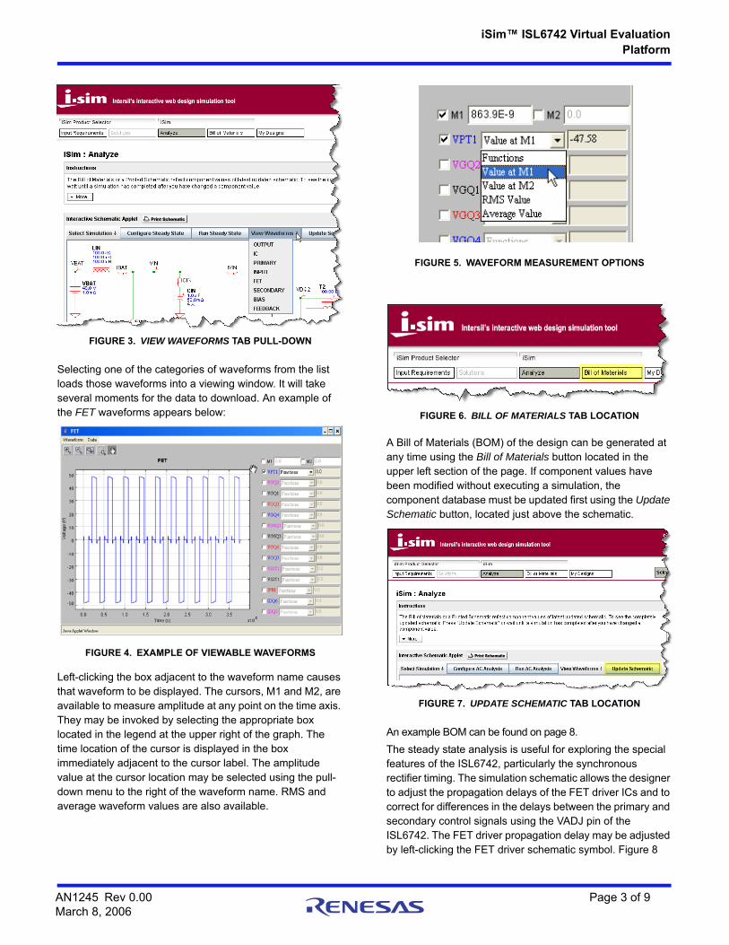
Selecting one of the categories of waveforms from the list loads those waveforms into a viewing window. It will take several moments for the data to download. An example of the FET waveforms appears below:
Left-clicking the box adjacent to the waveform name causes that waveform to be displayed. The cursors, M1 and M2, are available to measure amplitude at any point on the time axis. They may be invoked by selecting the appropriate box located in the legend at the upper right of the graph. The time location of the cursor is displayed in the box immediately adjacent to the cursor label. The amplitude value at the cursor location may be selected using the pull-down menu to the right of the waveform name. RMS and average waveform values are also available.
A Bill of Materials (BOM) of the design can be generated at any time using the Bill of Materials button located in the upper left section of the page. If component values have been modified without executing a simulation, the component database must be updated first using the Update Schematic button, located just above the schematic.
An example BOM can be found on page 8.
The steady state analysis is useful for exploring the special features of the ISL6742, particularly the synchronous rectifier timing. The simulation schematic allows the designer to adjust the propagation delays of the FET driver ICs and to correct for differences in the delays between the primary and secondary control signals using the VADJ pin of the ISL6742. The FET driver propagation delay may be adjusted by left-clicking the FET driver schematic symbol. Figure 8
FIGURE 3. VIEW WAVEFORMS TAB PULL-DOWN
FIGURE 4. EXAMPLE OF VIEWABLE WAVEFORMS
FIGURE 5. WAVEFORM MEASUREMENT OPTIONS
FIGURE 6. BILL OF MATERIALS TAB LOCATION
FIGURE 7. UPDATE SCHEMATIC TAB LOCATION
AN1245 Rev 0.00 Page 3 of 9March 8, 2006

iSim™ ISL6742 Virtual Evaluation
Platform
depicts the default SR timing using the drain-source voltage waveforms of Q6.
Although the primary side FET drivers are specified, the SR FET drivers are generic and have additional parameters available for adjustment. In particular, the rDSON and maximum drive current of the driver are adjustable. This allows the designer to match the drive capability to the requirements of the application.
Transient AnalysisThe Transient Analysis option allows the user to view the behavior of the power supply during a step load change to the converter output.
A Transient analysis is configured and executed much the same as the Steady State analysis. From the Select Simulation pull-down menu, select Transient Analysis. Adjust the duration of the simulated operation as desired from the Configure Transient Analysis tab. Selecting longer periods of operation will result in longer run times. Simulation times on the order of several minutes per 100s of operation can be expected. As before, the resulting waveforms can be viewed using the View Waveforms button when the simulation is finished.
Figure 9 shows the output voltage deviation caused by a 30A to 60A step load with a 100ns risetime on a 3.3V, 75A converter.
The transient analysis is useful for exploring the average current limit feature of the ISL6742. Figures 10 and 11 show the response of the current sense signal at CS and the resulting signal at IOUT. The average current for each inductor is captured by the sample and hold circuit on alternate half-cycles.
FIGURE 8. SR FET Q6 DRAIN-SOURCE VOLTAGE. TURN-ON NON-OVERLAP TIMING IS INDICATED BY M2-M1.
FIGURE 9. TRANSIENT ANALYSIS RESULTS FOR A 30A-60A OUTPUT STEP LOAD
FIGURE 10. CURRENT SENSE (CS) INPUT AND AVERAGE CURRENT (IOUT) SIGNAL WAVEFORMS RESULTING FROM AN OUTPUT STEP LOAD
AN1245 Rev 0.00 Page 4 of 9March 8, 2006

iSim™ ISL6742 Virtual Evaluation
Platform
Remembering the current-doubler output topology and that voltage-mode control is used, the stepped behavior of IOUT reflects the oscillation of the current in the output inductors due to the LC resonant tank formed by the DC blocking capacitor and the effective inductance in the primary. The output step load disturbs the tank circuit resulting in a damped oscillation. See Figure 12.
The average current limit circuit not only results in a very uniform current limit, but also corrects for the flux imbalance that occurs when peak current limit is used in voltage-mode controlled power supplies. The average current limit signal, IOUT, is integrated against a reference and the resulting signal modulates the error voltage, VERR. See Figure 14. Figure 13 shows the output response when the converter is placed in extended current limit. The response time of the average current limit circuit is user adjustable. In this
example, C11 and R12 were set to 220pF and 100, respectively, to shorten the simulation time. Like any closed loop feedback system, the average current limit circuit requires proper compensation to prevent oscillation.
When a step load exceeding the current limit setpoint is applied to the output of the power supply, several events occur. First, the peak current limit protects the power supply on a cycle-by-cycle basis until the average current limit circuit responds. Using peak current limit will cause a volt-second imbalance because the DC blocking capacitor charge is now controlled by the peak current limit rather than the volt-seconds across the transformer primary. This results in a net charge building up on the DC blocking capacitor and the bridge becomes unbalanced. The peak current limit
FIGURE 11. EXPANDED WAVEFORMS FROM FIGURE 10. NOTE THE SLIGHT DIFFERENCE IN AMPLITUDE OF THE ALTERNATE HALF-CYCLE CURRENT SENSE WAVEFORM.
FIGURE 12. VOLTAGE WAVEFORM ACROSS THE DC BLOCKING CAPACITOR C5
FIGURE 13.
FIGURE 14. VERR MODULATED BY THE AVERAGE CURRENT AMPLIFIER IN RESPONSE TO AN EXTENDED CURRENT LIMIT
AN1245 Rev 0.00 Page 5 of 9March 8, 2006

iSim™ ISL6742 Virtual Evaluation
Platform
starts to trip on one half-cycle only. If left unchecked, the DC blocking capacitor would eventually charge up to the supply rail.
The average current limit circuit prevents this behavior by forcing the same duty cycle on both half-cycles. Figure 15 shows the response of CS and IOUT to a step load into current limit. Initially CS is clipped at the 1 V peak current limit setpoint before the average current circuit limit responds. The average current limit circuits requires some time to damp oscillation on the DC blocking capacitor.
ConclusionThe ISL6742 iSim™ simulation tool provides the designer with a virtual test platform. More than just an educational tool, it allows the prospective designer to evaluate nearly all of the design decisions prior to committing resources to a physical realization.
ReferencesFor Intersil documents available on the web, see http://www.intersil.com/
[1] ISL6742 Data Sheet, Intersil Corporation, File No. FN9183.
FIGURE 15. IOUT AND CS RESULTING FROM A STEP LOAD INTO CURRENT LIMIT
AN1245 Rev 0.00 Page 6 of 9March 8, 2006

iSim™ ISL6742 Virtual Evaluation
Platform
ISL6742 iSim™ Simulation Schematic
AN1245 Rev 0.00 Page 7 of 9March 8, 2006

iSim™ ISL6742 Virtual Evaluation
Platform
ISL6742 Sample Bill of Materials (Default Values)
AN1245 Rev 0.00 Page 8 of 9March 8, 2006

http://www.renesas.comRefer to "http://www.renesas.com/" for the latest and detailed information.
Renesas Electronics America Inc.1001 Murphy Ranch Road, Milpitas, CA 95035, U.S.A.Tel: +1-408-432-8888, Fax: +1-408-434-5351Renesas Electronics Canada Limited9251 Yonge Street, Suite 8309 Richmond Hill, Ontario Canada L4C 9T3Tel: +1-905-237-2004Renesas Electronics Europe LimitedDukes Meadow, Millboard Road, Bourne End, Buckinghamshire, SL8 5FH, U.KTel: +44-1628-651-700, Fax: +44-1628-651-804Renesas Electronics Europe GmbHArcadiastrasse 10, 40472 Düsseldorf, Germany Tel: +49-211-6503-0, Fax: +49-211-6503-1327Renesas Electronics (China) Co., Ltd.Room 1709 Quantum Plaza, No.27 ZhichunLu, Haidian District, Beijing, 100191 P. R. ChinaTel: +86-10-8235-1155, Fax: +86-10-8235-7679Renesas Electronics (Shanghai) Co., Ltd.Unit 301, Tower A, Central Towers, 555 Langao Road, Putuo District, Shanghai, 200333 P. R. China Tel: +86-21-2226-0888, Fax: +86-21-2226-0999Renesas Electronics Hong Kong LimitedUnit 1601-1611, 16/F., Tower 2, Grand Century Place, 193 Prince Edward Road West, Mongkok, Kowloon, Hong KongTel: +852-2265-6688, Fax: +852 2886-9022Renesas Electronics Taiwan Co., Ltd.13F, No. 363, Fu Shing North Road, Taipei 10543, TaiwanTel: +886-2-8175-9600, Fax: +886 2-8175-9670Renesas Electronics Singapore Pte. Ltd.80 Bendemeer Road, Unit #06-02 Hyflux Innovation Centre, Singapore 339949Tel: +65-6213-0200, Fax: +65-6213-0300Renesas Electronics Malaysia Sdn.Bhd.Unit 1207, Block B, Menara Amcorp, Amcorp Trade Centre, No. 18, Jln Persiaran Barat, 46050 Petaling Jaya, Selangor Darul Ehsan, MalaysiaTel: +60-3-7955-9390, Fax: +60-3-7955-9510Renesas Electronics India Pvt. Ltd.No.777C, 100 Feet Road, HAL 2nd Stage, Indiranagar, Bangalore 560 038, IndiaTel: +91-80-67208700, Fax: +91-80-67208777Renesas Electronics Korea Co., Ltd.17F, KAMCO Yangjae Tower, 262, Gangnam-daero, Gangnam-gu, Seoul, 06265 KoreaTel: +82-2-558-3737, Fax: +82-2-558-5338
SALES OFFICES
© 2018 Renesas Electronics Corporation. All rights reserved.Colophon 7.0
(Rev.4.0-1 November 2017)
Notice
1. Descriptions of circuits, software and other related information in this document are provided only to illustrate the operation of semiconductor products and application examples. You are fully responsible for
the incorporation or any other use of the circuits, software, and information in the design of your product or system. Renesas Electronics disclaims any and all liability for any losses and damages incurred by
you or third parties arising from the use of these circuits, software, or information.
2. Renesas Electronics hereby expressly disclaims any warranties against and liability for infringement or any other claims involving patents, copyrights, or other intellectual property rights of third parties, by or
arising from the use of Renesas Electronics products or technical information described in this document, including but not limited to, the product data, drawings, charts, programs, algorithms, and application
examples.
3. No license, express, implied or otherwise, is granted hereby under any patents, copyrights or other intellectual property rights of Renesas Electronics or others.
4. You shall not alter, modify, copy, or reverse engineer any Renesas Electronics product, whether in whole or in part. Renesas Electronics disclaims any and all liability for any losses or damages incurred by
you or third parties arising from such alteration, modification, copying or reverse engineering.
5. Renesas Electronics products are classified according to the following two quality grades: “Standard” and “High Quality”. The intended applications for each Renesas Electronics product depends on the
product’s quality grade, as indicated below.
"Standard": Computers; office equipment; communications equipment; test and measurement equipment; audio and visual equipment; home electronic appliances; machine tools; personal electronic
equipment; industrial robots; etc.
"High Quality": Transportation equipment (automobiles, trains, ships, etc.); traffic control (traffic lights); large-scale communication equipment; key financial terminal systems; safety control equipment; etc.
Unless expressly designated as a high reliability product or a product for harsh environments in a Renesas Electronics data sheet or other Renesas Electronics document, Renesas Electronics products are
not intended or authorized for use in products or systems that may pose a direct threat to human life or bodily injury (artificial life support devices or systems; surgical implantations; etc.), or may cause
serious property damage (space system; undersea repeaters; nuclear power control systems; aircraft control systems; key plant systems; military equipment; etc.). Renesas Electronics disclaims any and all
liability for any damages or losses incurred by you or any third parties arising from the use of any Renesas Electronics product that is inconsistent with any Renesas Electronics data sheet, user’s manual or
other Renesas Electronics document.
6. When using Renesas Electronics products, refer to the latest product information (data sheets, user’s manuals, application notes, “General Notes for Handling and Using Semiconductor Devices” in the
reliability handbook, etc.), and ensure that usage conditions are within the ranges specified by Renesas Electronics with respect to maximum ratings, operating power supply voltage range, heat dissipation
characteristics, installation, etc. Renesas Electronics disclaims any and all liability for any malfunctions, failure or accident arising out of the use of Renesas Electronics products outside of such specified
ranges.
7. Although Renesas Electronics endeavors to improve the quality and reliability of Renesas Electronics products, semiconductor products have specific characteristics, such as the occurrence of failure at a
certain rate and malfunctions under certain use conditions. Unless designated as a high reliability product or a product for harsh environments in a Renesas Electronics data sheet or other Renesas
Electronics document, Renesas Electronics products are not subject to radiation resistance design. You are responsible for implementing safety measures to guard against the possibility of bodily injury, injury
or damage caused by fire, and/or danger to the public in the event of a failure or malfunction of Renesas Electronics products, such as safety design for hardware and software, including but not limited to
redundancy, fire control and malfunction prevention, appropriate treatment for aging degradation or any other appropriate measures. Because the evaluation of microcomputer software alone is very difficult
and impractical, you are responsible for evaluating the safety of the final products or systems manufactured by you.
8. Please contact a Renesas Electronics sales office for details as to environmental matters such as the environmental compatibility of each Renesas Electronics product. You are responsible for carefully and
sufficiently investigating applicable laws and regulations that regulate the inclusion or use of controlled substances, including without limitation, the EU RoHS Directive, and using Renesas Electronics
products in compliance with all these applicable laws and regulations. Renesas Electronics disclaims any and all liability for damages or losses occurring as a result of your noncompliance with applicable
laws and regulations.
9. Renesas Electronics products and technologies shall not be used for or incorporated into any products or systems whose manufacture, use, or sale is prohibited under any applicable domestic or foreign laws
or regulations. You shall comply with any applicable export control laws and regulations promulgated and administered by the governments of any countries asserting jurisdiction over the parties or
transactions.
10. It is the responsibility of the buyer or distributor of Renesas Electronics products, or any other party who distributes, disposes of, or otherwise sells or transfers the product to a third party, to notify such third
party in advance of the contents and conditions set forth in this document.
11. This document shall not be reprinted, reproduced or duplicated in any form, in whole or in part, without prior written consent of Renesas Electronics.
12. Please contact a Renesas Electronics sales office if you have any questions regarding the information contained in this document or Renesas Electronics products.
(Note 1) “Renesas Electronics” as used in this document means Renesas Electronics Corporation and also includes its directly or indirectly controlled subsidiaries.
(Note 2) “Renesas Electronics product(s)” means any product developed or manufactured by or for Renesas Electronics.


![Virtual Health Platform [05 Cr2 Cabrer Platform]](https://img.pdfslide.us/doc/110x75/55493080b4c9054c498c3535/virtual-health-platform-05-cr2-cabrer-platform.jpg)