Embed Size (px)
Citation preview
Application Note AN113
SWRA394 Page 1 of 20
Digital Wireless Microphone with Dual Radio Diversity By Michael Burns
Keywords Wireless Microphone Digital Microphone CC1110 CC1101
CC113L TLV320DAC32 TLV320AIC3104
1 Introduction
This Application Note is intended to show how the CC113 [1] value line low power RF receiver can be used together with a CC1110 [2] SOC transceiver to implement a low cost, high performance digital wireless microphone system.
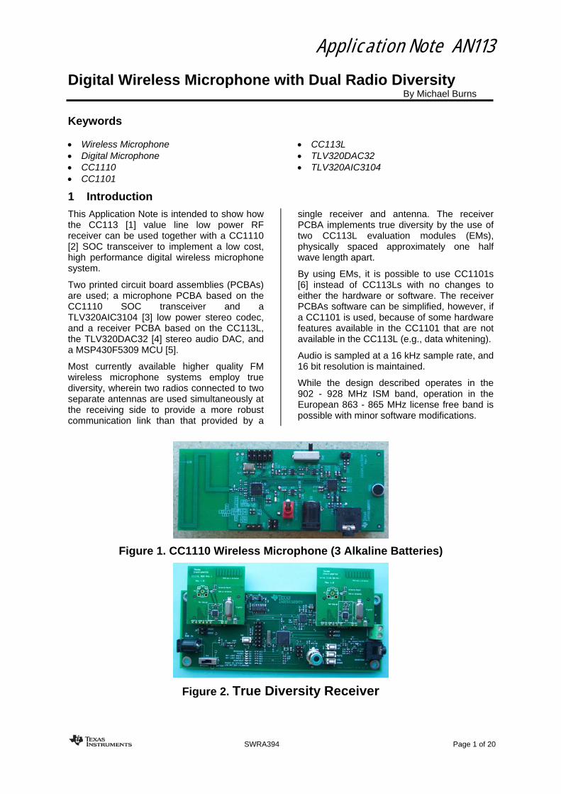
Two printed circuit board assemblies (PCBAs) are used; a microphone PCBA based on the CC1110 SOC transceiver and a TLV320AIC3104 [3] low power stereo codec, and a receiver PCBA based on the CC113L, the TLV320DAC32 [4] stereo audio DAC, and a MSP430F5309 MCU [5].
Most currently available higher quality FM wireless microphone systems employ true diversity, wherein two radios connected to two separate antennas are used simultaneously at the receiving side to provide a more robust communication link than that provided by a
single receiver and antenna. The receiver PCBA implements true diversity by the use of two CC113L evaluation modules (EMs), physically spaced approximately one half wave length apart.
By using EMs, it is possible to use CC1101s [6] instead of CC113Ls with no changes to either the hardware or software. The receiver PCBAs software can be simplified, however, if a CC1101 is used, because of some hardware features available in the CC1101 that are not available in the CC113L (e.g., data whitening).
Audio is sampled at a 16 kHz sample rate, and 16 bit resolution is maintained.
While the design described operates in the 902 - 928 MHz ISM band, operation in the European 863 - 865 MHz license free band is possible with minor software modifications.
Figure 1. CC1110 Wireless Microphone (3 Alkaline Batteries)
Figure 2. True Diversity Receiver
Application Note AN113
SWRA394 Page 2 of 20
Table of Contents KEYWORDS ..............................................................................................................................1 1 INTRODUCTION .............................................................................................................1 TABLE OF CONTENTS ............................................................................................................2 ABBREVIATIONS .....................................................................................................................2 2 MICROPHONE PCBA - OVERVIEW ..............................................................................3 3 MICROPHONE PCBA – DETAILED DESCRIPTION.....................................................4 4 RECEIVER BOARD – OVERVIEW.................................................................................5 5 RECEIVER BOARD – DETAILED DESCRIPTION ........................................................5 6 SOFTWARE DESCRIPTION – MICROPHONE..............................................................6 7 CC113L VERSUS CC1101 .............................................................................................7 8 SOFTWARE DESCRIPTION – RECEIVER ....................................................................8 9 CONCLUSION.................................................................................................................9 10 REFERENCES ..............................................................................................................20
Abbreviations
ADC Analogy to Digital Converter AGC Automatic Gain Control BALUN Balanced to Unbalanced (differential to single ended) transformer BCK (BCLK) Bit Clock CRC Cyclic Redundancy Check Codec Coder-Decoder DAC Digital to Analog Converter dB Decibel dBm Decibel (referenced to one milliWatt) DMA Direct Memory Access LDO Low Drop Out Multipath A phenomenon which occurs when electromagnetic waves bounce off of surfaces and
arrive either in phase (constructive) or out of phase (destructive interference). Endianness Refers to the order of bytes in a multi byte variable. For “big endian”, the most significant
byte precedes the least significant; for “little endian”, the least significant byte precedes the most significant.
EVM Evaluation and Verification Module FSK Frequency-Shift Keying GFSK Gaussian Frequency-Shift Keying GPIO General Purpose Input/Output I2C Inter-Integrated Circuit bus I2S Integrated Interchip Sound ISM Industrial, Scientific, Medical ISR Interrupt Service Routine LRCLK Left-Right Clock kbps kilobits per second MHz Megahertz mVpp millivolts peak-to-peak mW milliwatt NiCad NIckel CADmium NiMH NIckel-Metal Hydride PCB Printed Circuit Board PCBA Printed Circuit Board Assembly PER Packet Error Rate PLL Phase Locked Loop SOC System-On-Chip SPI Serial Peripheral Interface µs microseconds USCI Universal Serial Communication Interface VRMS Volts RMS (Root Mean Square)
Application Note AN113
SWRA394 Page 3 of 20
2 Microphone PCBA - Overview
The microphone PCBA is based on the TLV320ADC3104 Audio ADC and the CC1110 SOC RF transceiver. A block diagram is shown in Figure 5 and Figure 6. The ADC sample rate is 16 kHz with 16 bit resolution. This results in an audio bit rate of 256 kbps. In this application, the packet handling hardware features of the CC1110 are used. Refer to “Packet Handling Hardware Support” of [2] for details.
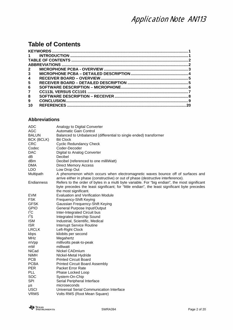
The CC1110’s packet format is shown in Figure 3. It includes a four byte preamble, a four byte sync word, a one byte address field (used to identify the transmitting device), data (the ADC samples), and two CRC bytes. For the sake of compatibility with SmartRF™ Studio software [7], a length byte is also included. The packet length is limited to 255 bytes, not including the preamble, sync word, and CRC bytes.
Figure 3. CC11xx Packet Format
Note that the additional twelve bytes (4 preamble bytes + 4 sync bytes + length byte + address byte + 2 CRC bytes) required by the packet handler results in the RF data rate (rate at which data is transmitted “over the air”) being greater than the audio data rate (rate at which the ADC is sampled).
Since packet overhead (12 bytes) is fixed, it is more efficient to send as much data as possible per packet (i.e., maximize packet length). However, the longer the packet, the more likely that interference can cause packet errors. As a compromise, 96 ADC samples (192 bytes) are sent in each data packet. A RF data rate of 300 kbps is used. GFSK modulation was selected, based on the recommendations of SmartRF™ Studio 7. Given the sample rate of 16 kHz, a packet is sent every 6 ms. At a RF data rate of 300 kbps, each packet takes 5.44 ms to transmit (((192+12)*8)/300000). The time required for the transmitter to transition from the IDLE state to the TX state (75.2 µs, see the CC1110 data sheet) must be added to this. This leaves approximately 6000 – (5440 + 75) or 485 µs of idle time between packets.
A four channel frequency hopping algorithm is employed. The RF channel is changed (incremented modulo 4) every packet, in a repeating pattern of four frequencies. In addition, the PCBA includes a three position band switch. The four channels in each of the three bands are unique. Frequency hopping is used to decrease the probability of packet loss due to multipath and/or intentional radiator interference.
Active_Channel_Index
Band 0 (time = n) 1 (time = n + 6 ms) 2 (time = n + 12 ms) 3 (time = n + 18 ms)
1 0 (f = 902.5 MHz) 20 (f = 907.5 MHz) 4 (f = 903.5 MHz) 16 (f = 906.5 MHz)
2 74 (f = 921.0 MHz) 98 (f = 927.0 MHz) 78 (f = 922.0 MHz) 94 (f = 926.0 MHz)
3 8 (f = 904.5 MHz) 82 (f = 923.0 MHz) 12 (f = 905.5 MHz) 90 (f = 925.0 MHz)
Table 1 - Frequency Hopping Channel Allocation
In Table 1, the transmitter carrier frequency is equal to the base frequency (902.5 MHz) plus the channel number times the channel spacing (250 kHz).
The TLV320AIC3104 supports sample rates of from 8 to 96 kHz. Included is an optional AGC, with programmable parameters (maximum gain, target output). For this design, only the left ADC is enabled. The digital control registers are interfaced via an I2C bus, created from two GPIO pins of the CC1110. Digital audio is interfaced to the CC1110 via an I2S bus.
Application Note AN113
SWRA394 Page 4 of 20
3 Microphone PCBA – Detailed Description
Refer to Figure 5. The Microphone PCBA requires only two active devices – the CC1110 RF transceiver and the TLV320AIC3104 audio codec, not including those devices required for supply voltage regulation. A small condenser style microphone is installed on the PCBA, along with a jack for an external microphone. The TLV320ADC3104 requires a master clock (MCLK), which is derived from timer 4 of the CC1110. The frequency of this clock signal (13 MHz) is one half of that of the CC1110’s 26.0 MHz crystal.
Two alternatives are shown for supplying power to the CC1110 and the codec. In Figure 6, power is supplied by two Ni-Cad, Ni-MH, or Alkaline batteries. In Figure 7, power is supplied by three Alkaline batteries. The digital logic of theTLV320AIC3104 requires a 1.8 V supply, which is derived from a TPS73018 LDO voltage regulator. Note that the CC1110 can operate with a supply voltage as low as 2.0 V.
Refer to Figure 6. The CC1110 and the I/O pins of the TLV320AIC3104 are connected directly to the batteries (VCCD). The supply voltage at the AVDD pin of the TLV320AIC3104 must have a minimum value of 2.6 V. Because the nominal output voltage of NiCad or NiMH cells is only 1.2 V, two cells wired in series will provide a nominal voltage of only 2.4 V, and it is therefore necessary to include a boost converter (TPS61097-33) to generate a voltage greater than 2.6 V (3.3 with the specified converter).
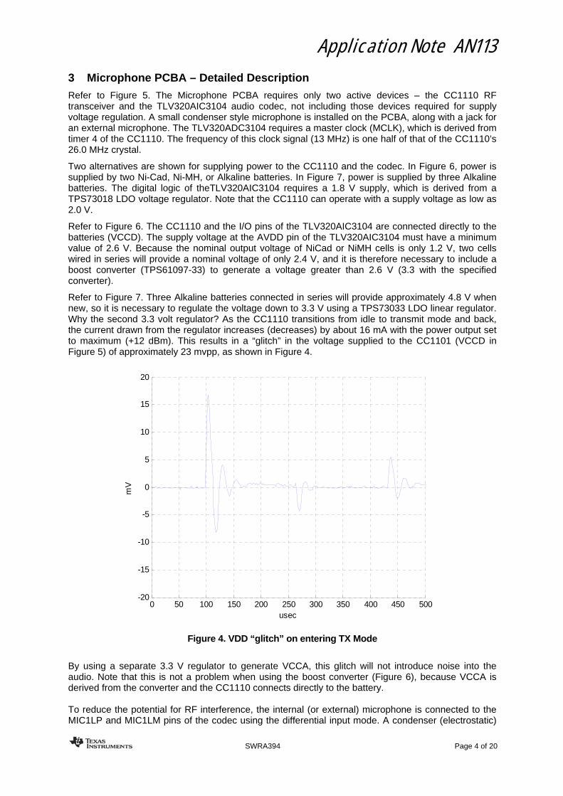
Refer to Figure 7. Three Alkaline batteries connected in series will provide approximately 4.8 V when new, so it is necessary to regulate the voltage down to 3.3 V using a TPS73033 LDO linear regulator. Why the second 3.3 volt regulator? As the CC1110 transitions from idle to transmit mode and back, the current drawn from the regulator increases (decreases) by about 16 mA with the power output set to maximum (+12 dBm). This results in a “glitch” in the voltage supplied to the CC1101 (VCCD in Figure 5) of approximately 23 mvpp, as shown in Figure 4.
0 50 100 150 200 250 300 350 400 450 500-20
-15
-10
-5
0
5
10
15
20
mV
usec
Figure 4. VDD “glitch” on entering TX Mode
By using a separate 3.3 V regulator to generate VCCA, this glitch will not introduce noise into the audio. Note that this is not a problem when using the boost converter (Figure 6), because VCCA is derived from the converter and the CC1110 connects directly to the battery. To reduce the potential for RF interference, the internal (or external) microphone is connected to the MIC1LP and MIC1LM pins of the codec using the differential input mode. A condenser (electrostatic)
Application Note AN113
SWRA394 Page 5 of 20
microphone requires a bias voltage; this is provided by the ADC at the MICBIAS pin. An external high level (up to 2 VRMS) signal can be used in place of a microphone, via the LINE2L input pin. The line input is enabled by installing a jumper on the “Select Aux In” pins of the “Option Jumpers” header.
The TLV320AIC3104 Audio CODEC includes an AGC (Automatic Gain Control). This prevents overloading the ADC on loud sounds (and the resulting distortion), while increasing microphone gain on soft sounds so that they may be more readily heard. Many AGC parameters are programmable, such as the target level, maximum gain, and attack and decay times. The AGC feature can be enabled or disabled via the “ENA AGC” jumper pins of the “Option Jumpers” header.
The PCB includes a meandered monopole antenna. Since the CC1110 has differential RF input/output pins, a four element passive network (balun) is used to convert the transceivers differential (balanced) RF input/output signals to a single ended (unbalanced) signal. A low pass filter is required to reduce the harmonic content of the transmitter to levels that comply with FCC regulations. Refer to Design Note DN017 [8] for details.
The CC1110 contains an internal ADC, which is used to monitor the battery voltage. When the battery voltage drops below approximately 2.2 V (Figure 6) or 3.6 V (Figure 7), the green LED is flashed at a 250 ms rate. If the battery voltage exceeds the threshold, the green LED will remain on.
4 Receiver Board – Overview
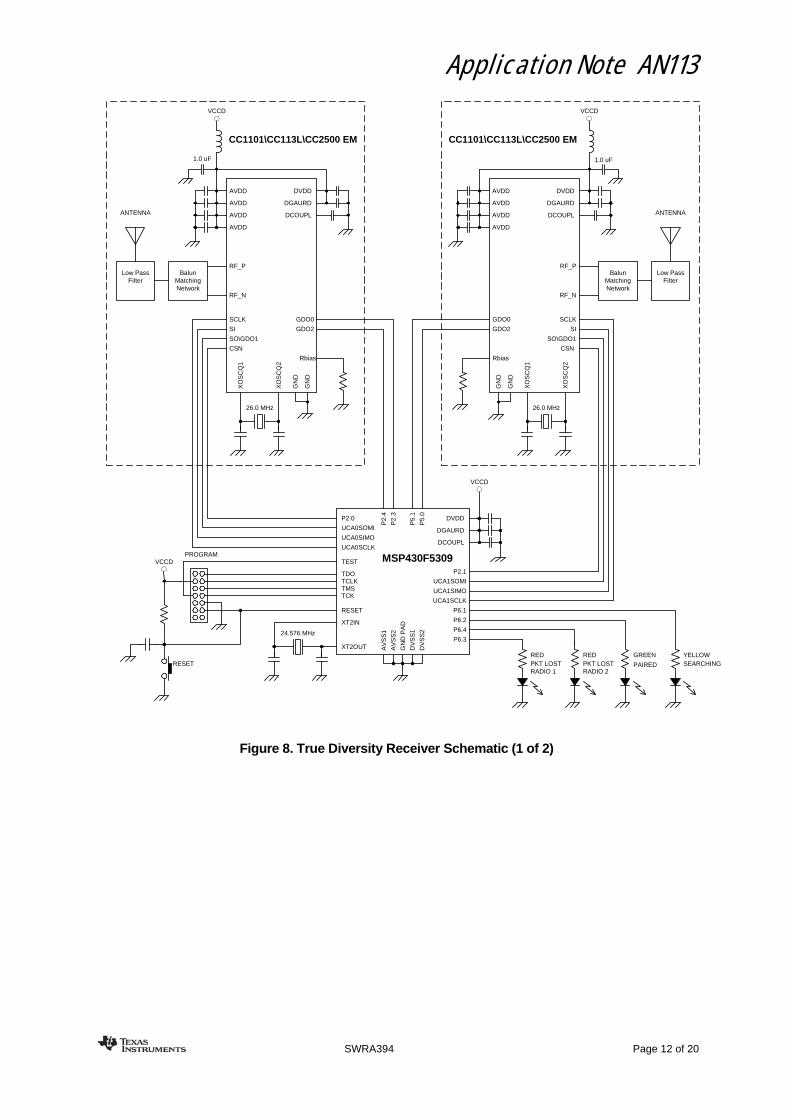
The receiver PCBA (“True Diversity Codec Dual Radios”) is based on the TLV320DAC32 audio DAC, the MSP430F5309 microprocessor, and the TPA6204 [9] mono class AB audio amplifier. Connectors are included for two CC1101 or CC113L EMs. A block diagram is shown in Figure 8 and Figure 9.
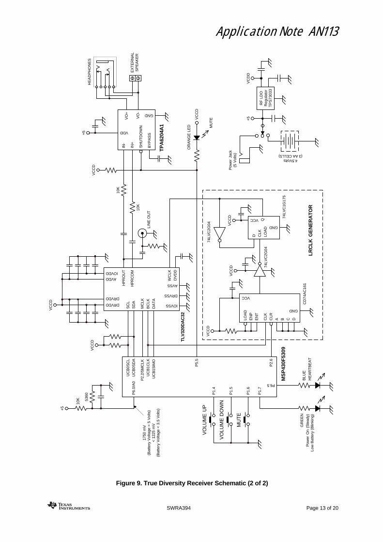
The TLV320DAC32 audio DAC is unusual in that it is “playback only” (i.e., it contains only DACs) and contains an internal LDO regulator for the digital core voltage supply. This eliminates the need for an external 1.8 V regulator, making it a cost effective solution for this application. The audio serial interface used is the “Left-Justified Data Format” (see “Digital Audio Data Serial Interface” of [3]). The MSP430F5309 does not include an I2S or Left-Justified audio bus interface. However, the SPI interface bus is similar, but lacks the required LRCLK (Left-Right Clock) signal. This can be generated by means of a 5 bit counter, as shown in Figure 9. Refer to [10] for details on this technique.
5 Receiver Board – Detailed Description
A detailed block diagram of the “True Diversity Codec Dual Radios” PCBA is shown in Figure 8 and Figure 9. Referring to Figure 8, the MSP430F5309 microcontroller is connected to two CC113L or CC1101 EMs via two USCIs (UCA0 and UCA1), operating in SPI mode.
Referring to Figure 9, the register interface of the TLV320DAC32 audio DAC is SPI compatible, and is interfaced to the MSPs UCB0 port. As was discussed in Section 4, the audio bus interface used to connect the codec to the MSP430F5309 uses the “Left-Justified” format, and is created from a SPI port (UCB1) by the addition of a LRCLK generator circuit (4 bit counter, ”D” type Flip-Flop, dual inverter). The TPA6204 is a 1.7-W fully differential class-AB mono audio amplifier. The gain has been set to four. This device has a SHUTDOWN input, which mutes the audio when low and is controlled by the MUTE push button switch via the MSP430 microcontroller. An orange LED will light when the TPA6204 is muted.
Headphone volume is controlled via the TLV320DAC32’s volume control registers. These registers provide attenuation of from 0 to -78.3 dB in 0.5 dB steps. The “Volume Up” and “Volume Down” push buttons set the attenuation value.
The codec MCLK signal is derived from pin P2.2 (SMCLK), which is set to 6.144 MHz, one quarter of the MSP430’s MCLK frequency (24.576 MHz). The choice of the MSP430’s MCLK frequency is constrained by three considerations:
1. The codec sample rate. In particular, the codec BCLK (Bit Clock) frequency must be set to 32 times the sample rate. BCLK is generated by the SPI bus controller (UCB1), and is derived from MCLK. BCLK must be an integer multiple of MCLK
2. The codec requires a 48 kHz reference frequency (Fsref). This is derived from the codec’s MCLK input (MSP430 SMCLK)
3. For accurate timing, MCLK should be an integer multiple of 1 ms
Application Note AN113
SWRA394 Page 6 of 20
With a SMCLK frequency of 6.144 MHz, all of these constraints are met. The required 48 kHz Fsref frequency is obtained by using the codec’s internal PLL, with P and R set to 1, J set to 16, and D set to 0. See the “Audio Clock Generation” section of [3] for details.
Table 2 shows the required BCLK divisor for the indicated sample rate.
Sample Rate (kHz) BCLK [kHz] BCLK Divisor
8 256 96
12 384 64
16 512 48
24 768 32
32 1024 24
48 1536 16
Table 2. BCLK Divisor
Low battery voltage detection is implemented using the MSP430’s internal ADC via pin P6.0 (A0). The trip voltage is set at approximately 3.5 V; the green LED will flash if the battery voltage drops below approximately 3.5 V, and remain lit if the battery voltage exceeds that value.
6 Software Description – Microphone
The software program for the microphone is divided into seven program segments as follows:
tw_main.c o Main program segment
tw_rf.c o Radio setup (initRF) o Configuration (rfConfigRadio) o Packet send (rfSendPacket)
tw_dma.c o dmaToRadio (from the TX buffer to the radio’s transmit data register, RFD, using
DMA channel 2) o dmaAudio (from the codec to the AudioIn buffers using DMA channel 4), o dmaMemtoMem (memory-to-memory using DMA channel 0), and the DMA interrupt
service routine. Init_peripherals.c
o Initializes the CC1110’s peripherals P0 through P2 I2S controller Timer 1 (generates an interrupt every 250 ms – used to flash the blue
Heartbeat and green Low Battery LEDs) Timer 3 (TX timeout) Timer 4 (used to generate codec MCLK).
init_codec.c o Initializes the TLV320AIC3104 codec control registers
i2c.c
o Implements a write only I2C interface using two DI/DO pins (I2C_SDA and I2C_SCL) o Subroutine I2Cwrite writes data into the specified codec register (page addr,
reg_addr).
tw_interrupt.c o handles radio and timer 1 interrupts
In addition, there are two “include” files. File board.h contains definition statements, option selections, and subroutine prototype declarations. File TLV320AIC3104.h contains definitions specific to the TLV320AIC3104 codec.
Application Note AN113
SWRA394 Page 7 of 20
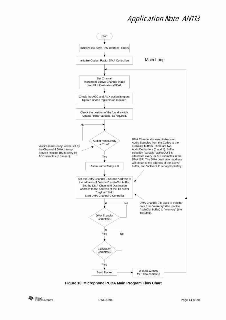
A flow chart of the Microphone PCBA’s main program (main) is shown in Figure 10. After initializing the I/O ports, I2S controller, timers, DMA controller, codec, and radio registers, the main program loop is entered. The main program loop is repeated every 6 ms.
At the beginning of the loop, the next channel is selected and PLL calibration started. The channel selected is based on the values of the band and Active_Channel_Index variables. There are three bands (0 – 2), with four channels (0 – 3) in each band. See Table 1. PLL calibration takes 180 µs to complete. While the PLL is calibrating, the status of the “ENA AGC” and “Select Aux In” jumpers are checked. If either has changed state from the previous loop, adjustments are made to the codec register settings as appropriate. Similarly, the position of the band switch is checked, and the value in variable band set accordingly.
Next, a check is made of the AudioFrameReady flag. This flag will be set by the DMA Channel 4 ISR every 96 ADC samples (6 ms). If set, DMA channel 0 is used to transfer CODEC data from the inactive audioOut buffer to the payload field of the TX buffer. Once the DMA transfer is complete and PLL calibration has finished, a packet is sent.
DMA channel 4 is driven by the I2S bus and is used to transfer ADC samples from the codec to the audioOut buffers. There are two audioOut buffers, the active buffer and the inactive buffer. Which buffer is active is identified by the value of the activeOut variable (0 or 1). The DMA controller will be set up to transfer ADC data into the active audioOut buffer. Note that the radio will take data from the inactive buffer when needed. Every 96 ADC samples, the DMA ISR will switch the DMA destination address to the address of the inactive buffer and toggle the ‘activeOut’ variable. At the same time, the AudioFrameReady flag will be set.
7 CC113L Versus CC1101
The CC113L value line receiver is a reduced cost, reduced function, receive only version of the CC1101. While it shares many of the same features and specifications as the CC1101, the CC113L does not support data whitening. Data Whitening improves PER by limiting the number of consecutive zeros and ones in the data stream, and can significantly improve PER in a streaming audio application, wherein the 16 bit samples can have small values when transmitting low sound levels. As a result, data whitening must be implemented in software when using the CC113L receiver. This is best accomplished using a table based algorithm, such as that described in Design Note DN509 [11].
The hardware based data whitening feature of the CC1110 is used on the microphone PCBA. Note that with whitening and CRC enabled, the CC1110 will whiten the CRC value. Consequently, CRC must be disabled on the receiver (CC113L) end of the link, because the CC113L will not de-whiten the CRC value. CRC must be implemented in software and the value in the PKTLEN register increased by two bytes – i.e., the last two bytes of the received packet will contain the whitened CRC value sent by the CC1110. Application Report SLAA221 “CRC Implementation with MSP430” [12] describes a CRC calculation algorithm that is table based and executes quickly, and is included in the receiver software.
Application Note AN113
SWRA394 Page 8 of 20
8 Software Description – Receiver
The software program for the receiver is divided into eight program segments as follows:
Main.c o Main program segment
Radio_Functions o Contains routines to write the radio control registers (write_Radio1_RFSettings,
write_Radio2_RFSettings) o Listen for a signal from the Microphone (ListenforBeacon) o Receive a packet using both radios (Receive_Packet_Dual)
init_Ports.c o Initializes the MSP430’s ports
Init_peripherals.c o Initializes the MSP430’s peripherals
The four USCI modules Timer A0 (generates an interrupt every ms – used to flash the blue Heartbeat
and green Low Battery LEDs, and to read the ADC) Timer A1 (used by the delay subroutine) Timer B (frame timer) ADC
TI_CC_spi.c o Subroutines to read and write the control registers of radio 1 and radio 2, and to issue
command strobes. The radio reset functions are also included in this segment. Misc_Subs.c
o Miscellaneous subroutines Delay ReadCodecRegister WriteCodecRegister LoadCodecRegs
ISR.c o Handles timer A0 and DMA channel 0 interrupts
PMM.c o Subroutine to increase the digital core voltage
In addition, there are three “include” files. TI_CC_hardware_board.h contains definition statements, option selections, and subroutine prototype declarations. TI_CC_CC1100-CC2500.h contains definitions specific to the CC110L, CC1101, and CC2500 radio families, including the configuration registers, strobe commands, and status registers.
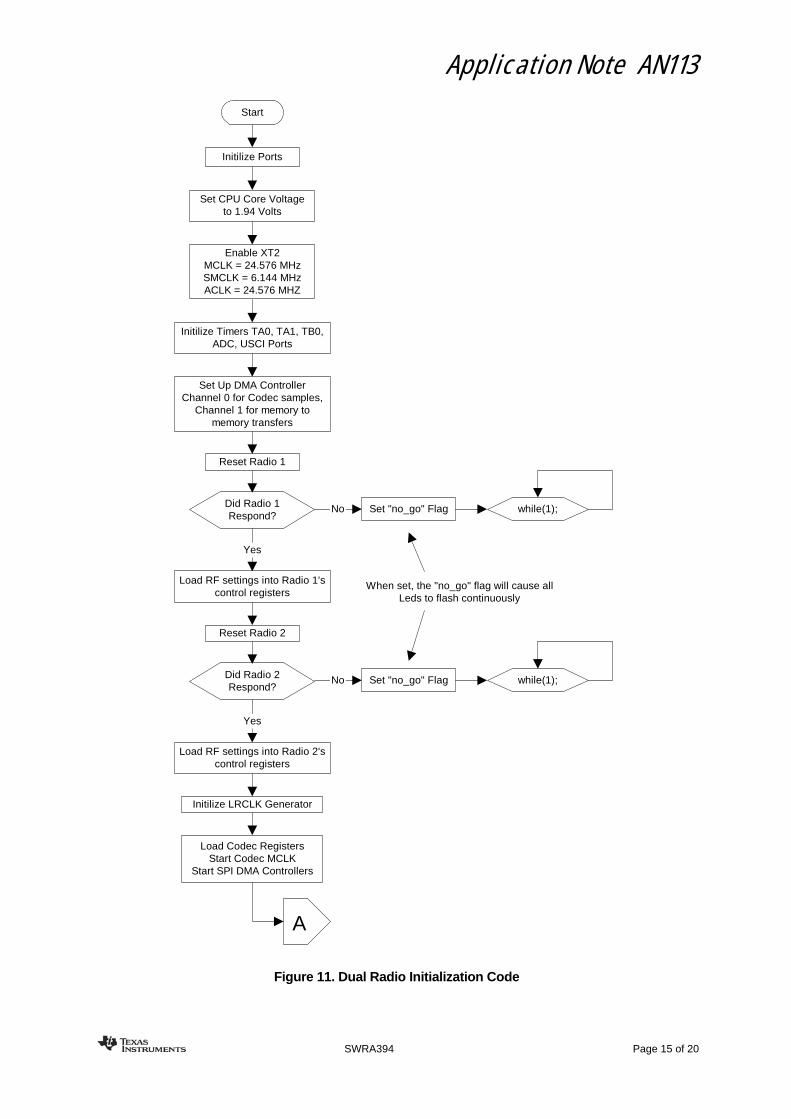
A flow chart of the microphone PCBA’s initialization program is shown in Figure 11. After initializing the I/O ports, clock, core voltage, timers, ADC, USCI controllers, DMA controller, codec, and radio registers, the main program loop is entered.
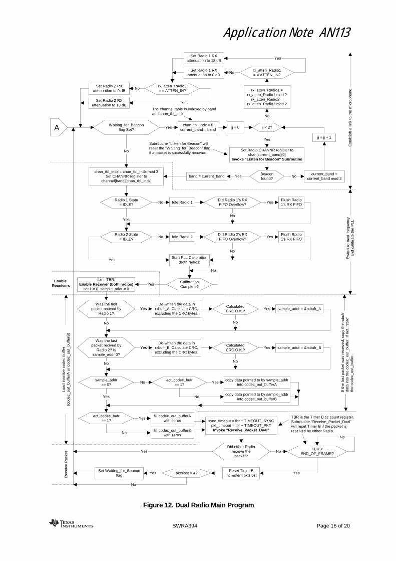
As is shown in Figure 12, the receiver board’s main program consists of five segments:
Segment 1 - “Establish a Link”: If the Waiting_for_Beacon flag is set, communications with the microphone board must be established. This flag will be set on board power up and if more than four consecutive packets have been lost. The key to this program segment is the Listen for Beacon subroutine, which, after calibrating the radios’ PLL, will enable both receivers (enter RX mode) for up to 27.5 ms. If a packet is received by either radio from the correct microphone (the SYSID byte of the received packet matches what is expected) during that period, the subroutine will exit with a return code of BEACON_FOUND. Note that this segment will first attempt to link using the first entry in the channel table of the current band. If a packet is not received, the band is incremented (modulo 3) and the Listen for Beacon subroutine is again invoked. This procedure is repeated with the receivers attenuator set to 0 db (no attenuation) and 18 dB until a link is established. If the expected microphone is out of range, the program will remain in segment 1.
Segment 2 - “Switch to Next Frequency and Calibrate the PLL”: This segment is straightforward, except that a check is made to verify that both radios are in the IDLE state and that the RX FIFO has not overflowed. These conditions are corrected if required.
Application Note AN113
SWRA394 Page 9 of 20
Segment 3 - “Enable Receivers”: The receivers of both radios are turned on. Variable tbr is set to the current frame timer (timer B) tic count, and will be used later in segment 5. Segment 4 - “Load Inactive Codec Buffer”: Data is copied from the rx_bufr of whichever receiver correctly received the last packet into the inactive codec_out_buffer. If neither radio received an error free packet, all samples in the inactive codec_out_buffer are set to zero. This “mutes” the audio for the duration of the missed packet. Note that the data in the Rx buffers must be de-whitened and the CRC value calculated before the CRC check can be performed.
Segment 5 - “Receive Packet”: Subroutine Receive_Packet_Dual is invoked. If the return code indicates that neither radio received the packet, the frame timer (timer B) is allowed to reach the END_OF_FRAME value and then reset. The “packets lost” counter (variable pktslost) is incremented and, if greater than four, the Waiting_for_Beacon flag is set. Program control is returned to segment 2 (if a packet was received) or segment 1 (if not). The main program loop is repeated every 6 ms (96 samples per packet, 16 kHz sample rate).
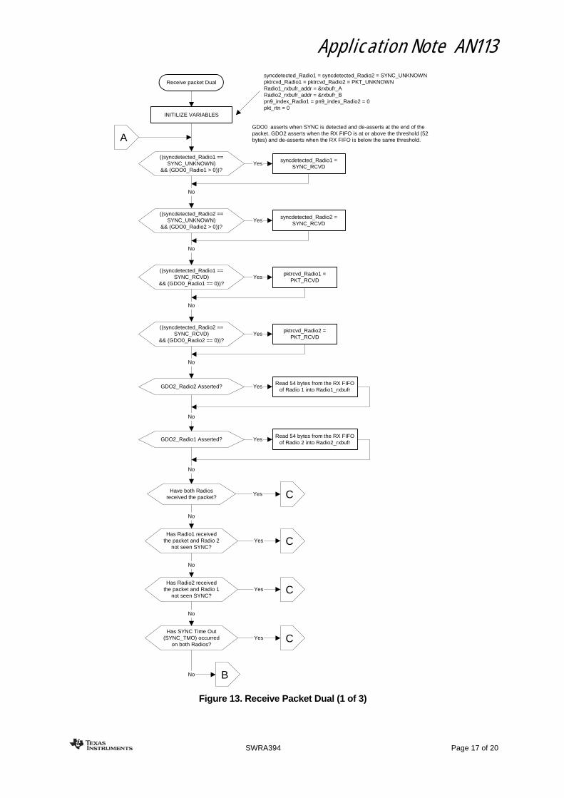
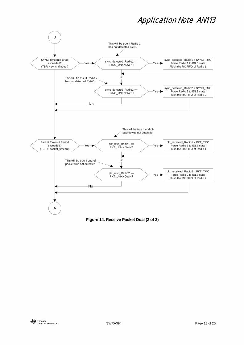
A flow chart for the Receive_Packet_Dual subroutine is shown in Figure 13 through Figure 15. The subroutine assumes that the receive mode has been enabled for both radios and that the frame timer (timer B) was reset following reception of the last packet. As shown in Figure 13 and Figure 14, program execution loops until one of five conditions is met:
1) Both radios have received the packet ((pktrcvd_Radio1 == PKT_RCVD) && (pktrcvd_Radio1 == PKT_RCVD))
2) Radio 1 has received a packet, but radio 2 failed to detect a sync word ((pktrcvd_Radio1 == PKT_RCVD) && (syncdetected_Radio2 == SYNC_TMO))
3) Radio 2 has received a packet, but radio 1 failed to detect a sync word ((pktrcvd_Radio2 == PKT_RCVD) && (syncdetected_Radio1 == SYNC_TMO))
4) Neither Radio detected a sync word before the SYNC timeout period expired ((syncdetected_Radio1 == SYNC_TMO) && (syncdetected_Radio2 == SYNC_TMO))
5) The packet timeout period has been exceeded (TBR > packet_timeout). TBR is the tic count register of Timer B.
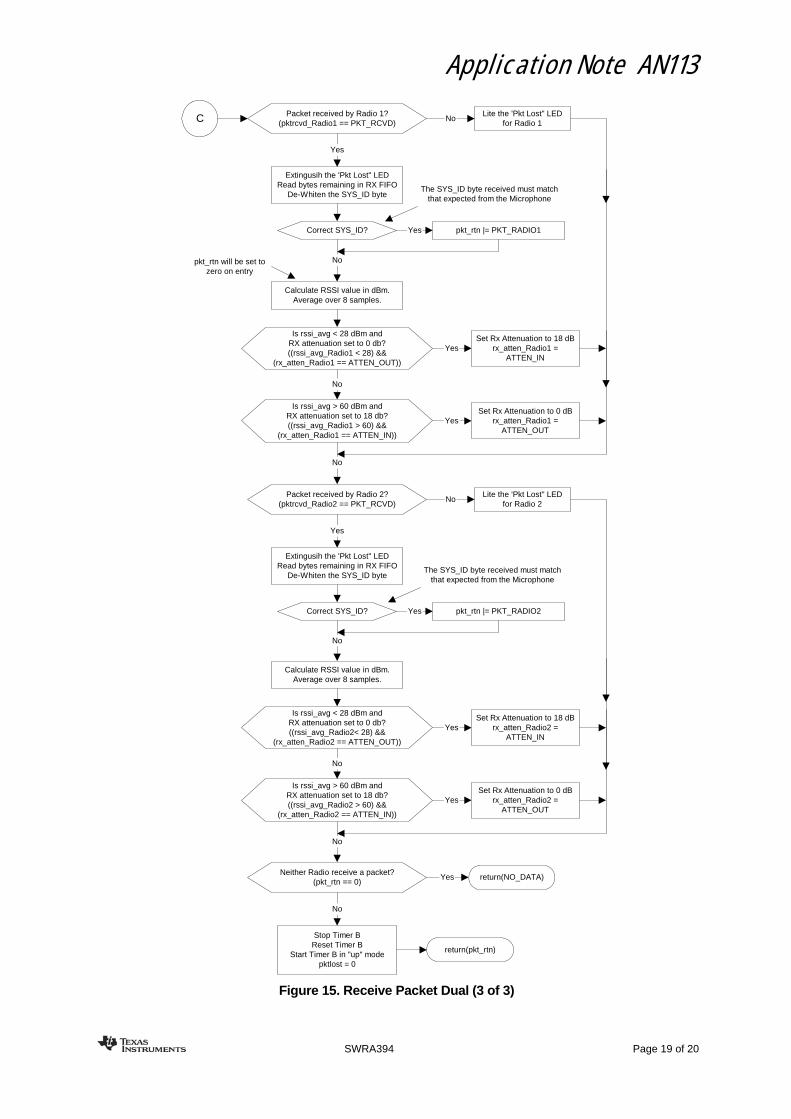
Once a sync word is detected, data is transferred from the radio’s RX FIFO to the rx_buffer every FIFO_THRESHOLD bytes (54), or until the end of the packet is detected. If a packet is received, the remaining bytes are read from the RX FIFO, the SYSID byte checked, and the return code set accordingly (Figure 15). The “Packet Lost” LEDs are also handled in this subroutine, as is RSSI (averaged over 8 samples) and any necessary adjustments to receiver attenuation. Finally, if a packet was received by either radio, the frame timer is reset and restarted and the “packets lost” counter (variable pktslost) zeroed.
9 Conclusion
This document has shown how the CC113L and CC1110 low power wireless transceivers can be used to implement a low cost, highly reliable wireless digital microphone. The design features true diversity by employing two radios with separate antennas used simultaneously.
Application Note AN113
SWRA394 Page 10 of 20
TLV320AIC3104
MCLK
BCLK
WCLK
DIN
DOUT
SDA
SCL
DVDD
DGAURD
DCOUPL
AVDD
RF_P
Rbias
26.0 MHz
XO
SC
Q1
XO
SC
Q2
CC1110
BalunMatchingNetwork
AVDD
AVDD
AVDD
RF_N
P2_0/T4CH0
P0_1/I2S CLK
P0_0/I2S WS
P1.7/I2S RX
P0_3
P0_4
P1_1
P1_0
P1_4
P0_2
BLUE
HEARTBEAT
MIC1LP
MIC1LM
VCCD+1.8
INTERNALMICROPHONE
LINE IN
RESET
RESETP1_4
P2_2/DC
P2_1/DD
PROGRAM
VCCD
P0_5
P1_3
SEL AUX IN
ENA AGC
VCCAVCCD
IOV
DD
DV
DD
DR
VD
DD
RV
DD
AV
DD
MICBIAS
EXTERNALMICROPHONE
LINE2L
Power On (Steady)Low Battery (Blinking)
GREEN
P1_2
BANDSWITCH
Low PassFilter
PRINTED CIRCUITBOARD
ANTENNA
VCCD
+5
P0_7/ADC7
INTERNAL TOCC1110
OPTION JUMPERSHEADER
Figure 5. Microphone PCBA Block Diagram
Application Note AN113
SWRA394 Page 11 of 20
VCCD
RF LDORegulatorTPS73018
+1.8VBAT
2.4
Vo
lts(2
NiC
ad C
ELL
S)
VCCA
Vout
Vin
ENA
L
TPS61097
Figure 6 - Microphone PCBA Power (2 NiCad Batteries)
RF LDORegulatorTPS73033
VCCD
RF LDORegulatorTPS73018
+1.8VBAT
4.5
Vo
lts(3
AA
A C
EL
LS
)
External Power(5 Volts)
RF LDORegulatorTPS73033
VCCA
Figure 7. Microphone PCBA Power (3 Alkaline Batteries)
Application Note AN113
SWRA394 Page 12 of 20
DVDD
DGAURD
DCOUPL
AVDD
RF_P
Rbias
26.0 MHz
XO
SC
Q1
XO
SC
Q2
BalunMatchingNetwork
AVDD
AVDD
AVDD
RF_N
GDO0
SI
SO\GDO1
CSN
SCLK
Low PassFilter
ANTENNA
VCCD
GN
D
GN
D
GDO2
1.0 uF
CC1101\CC113L\CC2500 EM
DVDD
DGAURD
DCOUPL
AVDD
RF_P
Rbias
26.0 MHz
XO
SC
Q1
XO
SC
Q2
BalunMatchingNetwork
AVDD
AVDD
AVDD
RF_N
GDO0
SI
SO\GDO1
CSN
SCLK
Low PassFilter
ANTENNA
VCCD
GN
D
GN
D
GDO2
1.0 uF
AV
SS
1
AV
SS
2
GN
D P
AD
DV
SS
1
DV
SS
224.576 MHz
XT2IN
XT2OUT
P2.0
UCA0SOMI
UCA0SIMO
UCA0SCLK
P2.1
UCA1SOMI
UCA1SIMO
UCA1SCLK
P2
.4
P2
.3
P5
.1
P5
.0 DVDD
DGAURD
DCOUPL
VCCD
PROGRAMTEST
TDOTCLKTMSTCK
RESET
VCCD
RESET
MSP430F5309
REDPKT LOSTRADIO 1
REDPKT LOSTRADIO 2
YELLOWSEARCHING
GREEN
PAIRED
P6.1
P6.2
P6.4
P6.3
CC1101\CC113L\CC2500 EM
Figure 8. True Diversity Receiver Schematic (1 of 2)
Application Note AN113
SWRA394 Page 13 of 20
RF
LD
OR
egu
lato
rT
PS
730
33
4.5Volts(3 AA CELLS)
Pow
er J
ack
(5 V
olts
)
BLU
E
HE
AR
TB
EA
TP
ower
On
(Ste
ady)
Low
Bat
tery
(B
linki
ng)
GR
EE
N
VC
CD DRVDD
IOVDD
WC
LK
DA
TA
BC
LK
MC
LKP
2.2/
SM
CLK
UC
B1S
IMO
UC
B1
CL
K
SC
L
SD
A
UC
B0
SC
L
UC
B0
SD
A
CL
K
CL
R
LOA
D
EN
P
EN
T
VC
CD
A B C D
P2
.6
TL
V32
0DA
C32
VC
CD
VC
CD VCC
D CLK
QLO
AD
GND
74LV
C2G
04
74L
VC
2G
04
74LV
C1G
175
CD
74A
C16
1
VCC
GND
LR
CL
K G
EN
ER
AT
OR
DRVSS
AVSS
VO
+
IN+
SH
UT
DO
WN
BY
PA
SS
EX
TE
RN
AL
SP
EA
KE
R
HE
AD
PH
ON
ES
+5 VDD
GND
IN-
VO
-
10K
10K
VC
CD
OR
AN
GE
LE
D MU
TE
P5
.5
+5
VC
DD
VO
LUM
E D
OW
N
MU
TE
VO
LUM
E U
P
P1.
4
P1.
5
P1.
6
P1.
7
P6.5
+5
P6.
0/A
0
10K 53
60
1750
mV
(Bat
tery
Vo
ltage
= 5
Vol
ts)
< 1
225
mV
(Ba
ttery
Vol
tag
e <
3.5
Vol
ts)
LIN
E O
UT
HP
RO
UT
DV
DD
TP
A62
04A
1
MS
P43
0F53
09
DRVDD
AVDD
IOVSS
VC
CD
HP
RC
OM
VC
CD
Figure 9. True Diversity Receiver Schematic (2 of 2)
Application Note AN113
SWRA394 Page 14 of 20
Start
Initialize Codec, Radio, DMA Controllers
Set ChannelIncrement 'Active Channel' index
Start PLL Calibration (SCAL)
AudioFrameReady= True?
No
Yes
CalibrationComplete?
No
Send Packet
Yes
Main Loop
'AudioFrameReady' will be set bythe Channel 4 DMA InteruptService Routine (ISR) every 96ADC samples (6.0 msec).
Initialize I/O ports, I2S interface, timers
AudioFrameReady = 0
Set the DMA Channel 0 Source Address tothe address of "inactive" audioOut buffer.
Set the DMA Channel 0 DestinationAddress to the address of the TX buffer
"payload" fieldStart DMA Channel 0 Controller
DMA TransferComplete?
No
Wait 5612 usecfor TX to complete
DMA Channel 4 is used to transferAudio Samples from the Codec to theaudioOut buffers. There are twoAudioOut buffers (0 and 1). Bufferselection [variable "activeOut"] isalternated every 96 ADC samples in theDMA ISR. The DMA destination addresswill be set to the address of the 'active'buffer, and "activeOut" set appropriately.
DMA Channel 0 is used to transferdata from "memory" (the inactiveAudioOut buffer) to "memory" (theTxBuffer).
Check the AGC and AUX option jumpers.Update Codec registers as required.
Check the position of the 'band' switch.Update "band' variable as required.
Yes
Figure 10. Microphone PCBA Main Program Flow Chart
Application Note AN113
SWRA394 Page 15 of 20
Start
Initilize Ports
Set CPU Core Voltageto 1.94 Volts
Enable XT2MCLK = 24.576 MHzSMCLK = 6.144 MHzACLK = 24.576 MHZ
Initilize Timers TA0, TA1, TB0,ADC, USCI Ports
Set Up DMA ControllerChannel 0 for Codec samples,
Channel 1 for memory tomemory transfers
Reset Radio 1
Did Radio 1Respond?
No Set "no_go" Flag
Yes
Load RF settings into Radio 1'scontrol registers
Reset Radio 2
Did Radio 2Respond?
No Set "no_go" Flag
Yes
Load RF settings into Radio 2'scontrol registers
Initilize LRCLK Generator
Load Codec RegistersStart Codec MCLK
Start SPI DMA Controllers
while(1);
while(1);
When set, the "no_go" flag will cause allLeds to flash continuously
A
Figure 11. Dual Radio Initialization Code
Application Note AN113
SWRA394 Page 16 of 20
Waiting_for_Beaconflag Set?
Yeschan_tbl_indx = 0
current_band = band
The channel table is indexed by bandand chan_tbl_indx.
jj < 2?jj = 0
Yes
Set Radio CHANNR register tochan[current_band][0]
Invoke "Listen for Beacon" Subroutine
Beaconfound?
Nocurrent_band =
current_band mod 3
jj = jj + 1
band = current_band Yes
No
A
No
rx_atten_Radio1 =rx_atten_Radio1 mod 2
rx_atten_Radio2 =rx_atten_Radio2 mod 2
rx_atten_Radio1= = ATTEN_IN?
Set Radio 1 RXattenuation to 18 dB
Yes
Set Radio 1 RXattenuation to 0 dB
No
rx_atten_Radio2= = ATTEN_IN?
Set Radio 2 RXattenuation to 18 dB
Yes
Set Radio 2 RXattenuation to 0 dB
No
chan_tbl_indx = chan_tbl_indx mod 3Set CHANNR register to
channel[band][chan_tbl_indx]
Radio 1 State= IDLE?
NoDid Radio 1's RXFIFO Overflow?
Idle Radio 1 YesFlush Radio1's RX FIFO
NoYes
Radio 2 State= IDLE?
NoDid Radio 2's RXFIFO Overflow?
Idle Radio 2 YesFlush Radio1's RX FIFO
No
YesStart PLL Calibration
(both radios)
CalibrationComplete?
No
Yestbr = TBR;
Enable Receiver (both radios)set k = 0, sample_addr = 0
Was the lastpacket recived by
Radio 1?Yes
De-whiten the data inrxbufr_A. Calculate CRC,excluding the CRC bytes.
CalculatedCRC O.K.?
sample_addr = &rxbufr_AYes
No
Was the lastpacket recived by
Radio 2? Issample_addr 0?
YesDe-whiten the data in
rxbufr_B. Calculate CRC,excluding the CRC bytes.
CalculatedCRC O.K.?
sample_addr = &rxbufr_BYes
No
No
sample_addr== 0?
act_codec_bufr== 1?
No Yescopy data pointed to by sample_addr
into codec_out_bufferA
No
act_codec_bufr== 1?
Yesfill codec_out_bufferA
with zeros
Nofill codec_out_bufferB
with zeros
copy data pointed to by sample_addrinto codec_out_bufferB
Yes
sync_timeout = tbr + TIMEOUT_SYNCpkt_timeout = tbr + TIMEOUT_PKTInvoke "Receive_Packet_Dual"
Did either Radioreceive the
packet?
TBR <END_OF_FRAME?
No
NoYes
YesReset Timer B
Increment pktslostpktslost > 4?Yes
Set Waiting_for_Beaconflag
No
TBR is the Timer B tic count register.Subroutine "Receive_Packet_Dual"will reset Timer B if the packet isreceived by either Radio.
Subroutine "Listen for Beacon" willreset the "Waiting_for_Beacon" flagif a packet is sucessfully received.
Est
ab
lish
a li
nk t
o t
he m
icro
ph
one
Sw
itch
to n
ext
freq
uenc
ya
nd
calib
rate
th
e P
LL
No
If th
e la
st p
ack
et w
as
rece
ive
d,
copy
th
e r
xbu
frda
ta in
to t
he
co
de
c_o
ut_
buff
er.
If
not
, "z
ero
'th
e c
ode
c_o
ut_
bu
ffer.
Enable Receivers
Loa
d in
act
ive
co
dec
bu
ffer
(co
dec_
out
_b
uffe
rA o
r co
de
c_o
ut_
buff
erB
)R
ece
ive
Pa
cke
t
Figure 12. Dual Radio Main Program
Application Note AN113
SWRA394 Page 17 of 20
Receive packet Dual
INITILIZE VARIABLES
((syncdetected_Radio1 ==SYNC_UNKNOWN)
&& (GDO0_Radio1 > 0))?
syncdetected_Radio1 =SYNC_RCVD
Yes
No
((syncdetected_Radio2 ==SYNC_UNKNOWN)
&& (GDO0_Radio2 > 0))?
syncdetected_Radio2 =SYNC_RCVD
Yes
No
((syncdetected_Radio1 ==SYNC_RCVD)
&& (GDO0_Radio1 == 0))?
pktrcvd_Radio1 =PKT_RCVD
Yes
No
((syncdetected_Radio2 ==SYNC_RCVD)
&& (GDO0_Radio2 == 0))?
pktrcvd_Radio2 =PKT_RCVD
Yes
No
GDO2_Radio2 Asserted? Yes
No
Read 54 bytes from the RX FIFOof Radio 1 into Radio1_rxbufr
GDO2_Radio1 Asserted? Yes
No
Read 54 bytes from the RX FIFOof Radio 2 into Radio2_rxbufr
Have both Radiosreceived the packet?
No
Has Radio1 receivedthe packet and Radio 2
not seen SYNC?
No
Has Radio2 receivedthe packet and Radio 1
not seen SYNC?
No
Has SYNC Time Out(SYNC_TMO) occurred
on both Radios?
No
Yes
Yes
Yes
Yes
syncdetected_Radio1 = syncdetected_Radio2 = SYNC_UNKNOWNpktrcvd_Radio1 = pktrcvd_Radio2 = PKT_UNKNOWNRadio1_rxbufr_addr = &rxbufr_ARadio2_rxbufr_addr = &rxbufr_Bpn9_index_Radio1 = pn9_index_Radio2 = 0pkt_rtn = 0
GDO0 asserts when SYNC is detected and de-asserts at the end of thepacket. GDO2 asserts when the RX FIFO is at or above the threshold (52bytes) and de-asserts when the RX FIFO is below the same threshold.A
C
C
C
C
B
Figure 13. Receive Packet Dual (1 of 3)
Application Note AN113
SWRA394 Page 18 of 20
SYNC Timeout Periodexceeded?
(TBR > sync_timeout)Yes
B
sync_detected_Radio1 ==SYNC_UNKNOWN?
sync_detected_Radio1 = SYNC_TMOForce Radio 1 to IDLE state
Flush the RX FIFO of Radio 1
No
Yes
sync_detected_Radio2 ==SYNC_UNKNOWN?
sync_detected_Radio2 = SYNC_TMOForce Radio 2 to IDLE state
Flush the RX FIFO of Radio 2Yes
Packet Timeout Periodexceeded?
(TBR > packet_timeout)Yes
pkt_rcvd_Radio1 ==PKT_UNKNOWN?
pkt_received_Radio1 = PKT_TMOForce Radio 1 to IDLE state
Flush the RX FIFO of Radio 1
No
Yes
pkt_rcvd_Radio2 ==PKT_UNKNOWN?
pkt_received_Radio2 = PKT_TMOForce Radio 2 to IDLE state
Flush the RX FIFO of Radio 2Yes
No
A
No
This will be true if end-of-packet was not detected
This will be true if end-of-packet was not detected
This will be true if Radio 1has not detected SYNC
This will be true if Radio 2has not detected SYNC
Figure 14. Receive Packet Dual (2 of 3)
Application Note AN113
SWRA394 Page 19 of 20
C Packet received by Radio 1?(pktrcvd_Radio1 == PKT_RCVD)
Extingusih the 'Pkt Lost" LEDRead bytes remaining in RX FIFO
De-Whiten the SYS_ID byte
Yes
Lite the 'Pkt Lost" LEDfor Radio 1
Calculate RSSI value in dBm.Average over 8 samples.
No
Is rssi_avg < 28 dBm andRX attenuation set to 0 db?((rssi_avg_Radio1 < 28) &&
(rx_atten_Radio1 == ATTEN_OUT))
YesSet Rx Attenuation to 18 dB
rx_atten_Radio1 =ATTEN_IN
No
Is rssi_avg > 60 dBm andRX attenuation set to 18 db?((rssi_avg_Radio1 > 60) &&
(rx_atten_Radio1 == ATTEN_IN))
YesSet Rx Attenuation to 0 dB
rx_atten_Radio1 =ATTEN_OUT
Packet received by Radio 2?(pktrcvd_Radio2 == PKT_RCVD)
Yes
Lite the 'Pkt Lost" LEDfor Radio 2
Calculate RSSI value in dBm.Average over 8 samples.
No
Is rssi_avg < 28 dBm andRX attenuation set to 0 db?((rssi_avg_Radio2< 28) &&
(rx_atten_Radio2 == ATTEN_OUT))
YesSet Rx Attenuation to 18 dB
rx_atten_Radio2 =ATTEN_IN
No
Is rssi_avg > 60 dBm andRX attenuation set to 18 db?((rssi_avg_Radio2 > 60) &&
(rx_atten_Radio2 == ATTEN_IN))
YesSet Rx Attenuation to 0 dB
rx_atten_Radio2 =ATTEN_OUT
No
No
Neither Radio receive a packet?(pkt_rtn == 0)
return(NO_DATA)Yes
No
Stop Timer BReset Timer B
Start Timer B in "up" modepktlost = 0
return(pkt_rtn)
Correct SYS_ID? Yes pkt_rtn |= PKT_RADIO1
No
Extingusih the 'Pkt Lost" LEDRead bytes remaining in RX FIFO
De-Whiten the SYS_ID byte
pkt_rtn will be set tozero on entry
The SYS_ID byte received must matchthat expected from the Microphone
Correct SYS_ID? Yes pkt_rtn |= PKT_RADIO2
No
The SYS_ID byte received must matchthat expected from the Microphone
Figure 15. Receive Packet Dual (3 of 3)
Application Note AN113
SWRA394 Page 20 of 20
10 References
[1] CC113L Value Line Receiver (CC113L)
[2] CC1110Fx/CC1111Fx Low-Power Sub-1 GHz RF System-on-Chip (SoC) with MCU, Memory, Transceiver, and USB Controller (CC1110F32)
[3] TLV320AIC3104 Low Power Stereo Audio CODEC For Portable Audio/Telephony (TLV320AIC3104)
[4] TLV320DAC32 Low Power Stereo Audio DAC for Portable Audio/Telephony (TLV320DAC32)
[5] MSP430F5309 Mixed Signal Microcontroller (MSP430F309)
[6] CC1101 Low-Power Sub-1 GHz RF Transceiver (CC1101)
[7] SmartRF™ Studio 7 (SWRC176)
[8] DN017 - CC11xx 868/915 MHz RF Matching (SWRA168)
[9] TPA6204 1.7-W Mono Fully Differential Audio Power Amplifier (TPA6204A1)
[10] Interfacing an I2S Device to a MSP430 Device (SLAA49)
[11] DN509 - Data Whitening and Random TX Mode (DN509)
[12] CRC Implementation With MSP430 (SLAA221)
IMPORTANT NOTICE
Texas Instruments Incorporated and its subsidiaries (TI) reserve the right to make corrections, modifications, enhancements, improvements,and other changes to its products and services at any time and to discontinue any product or service without notice. Customers shouldobtain the latest relevant information before placing orders and should verify that such information is current and complete. All products aresold subject to TI’s terms and conditions of sale supplied at the time of order acknowledgment.
TI warrants performance of its hardware products to the specifications applicable at the time of sale in accordance with TI’s standardwarranty. Testing and other quality control techniques are used to the extent TI deems necessary to support this warranty. Except wheremandated by government requirements, testing of all parameters of each product is not necessarily performed.
TI assumes no liability for applications assistance or customer product design. Customers are responsible for their products andapplications using TI components. To minimize the risks associated with customer products and applications, customers should provideadequate design and operating safeguards.
TI does not warrant or represent that any license, either express or implied, is granted under any TI patent right, copyright, mask work right,or other TI intellectual property right relating to any combination, machine, or process in which TI products or services are used. Informationpublished by TI regarding third-party products or services does not constitute a license from TI to use such products or services or awarranty or endorsement thereof. Use of such information may require a license from a third party under the patents or other intellectualproperty of the third party, or a license from TI under the patents or other intellectual property of TI.
Reproduction of TI information in TI data books or data sheets is permissible only if reproduction is without alteration and is accompaniedby all associated warranties, conditions, limitations, and notices. Reproduction of this information with alteration is an unfair and deceptivebusiness practice. TI is not responsible or liable for such altered documentation. Information of third parties may be subject to additionalrestrictions.
Resale of TI products or services with statements different from or beyond the parameters stated by TI for that product or service voids allexpress and any implied warranties for the associated TI product or service and is an unfair and deceptive business practice. TI is notresponsible or liable for any such statements.
TI products are not authorized for use in safety-critical applications (such as life support) where a failure of the TI product would reasonablybe expected to cause severe personal injury or death, unless officers of the parties have executed an agreement specifically governingsuch use. Buyers represent that they have all necessary expertise in the safety and regulatory ramifications of their applications, andacknowledge and agree that they are solely responsible for all legal, regulatory and safety-related requirements concerning their productsand any use of TI products in such safety-critical applications, notwithstanding any applications-related information or support that may beprovided by TI. Further, Buyers must fully indemnify TI and its representatives against any damages arising out of the use of TI products insuch safety-critical applications.
TI products are neither designed nor intended for use in military/aerospace applications or environments unless the TI products arespecifically designated by TI as military-grade or "enhanced plastic." Only products designated by TI as military-grade meet militaryspecifications. Buyers acknowledge and agree that any such use of TI products which TI has not designated as military-grade is solely atthe Buyer's risk, and that they are solely responsible for compliance with all legal and regulatory requirements in connection with such use.
TI products are neither designed nor intended for use in automotive applications or environments unless the specific TI products aredesignated by TI as compliant with ISO/TS 16949 requirements. Buyers acknowledge and agree that, if they use any non-designatedproducts in automotive applications, TI will not be responsible for any failure to meet such requirements.
Following are URLs where you can obtain information on other Texas Instruments products and application solutions:
Products Applications
Audio www.ti.com/audio Communications and Telecom www.ti.com/communications
Amplifiers amplifier.ti.com Computers and Peripherals www.ti.com/computers
Data Converters dataconverter.ti.com Consumer Electronics www.ti.com/consumer-apps
DLP® Products www.dlp.com Energy and Lighting www.ti.com/energy
DSP dsp.ti.com Industrial www.ti.com/industrial
Clocks and Timers www.ti.com/clocks Medical www.ti.com/medical
Interface interface.ti.com Security www.ti.com/security
Logic logic.ti.com Space, Avionics and Defense www.ti.com/space-avionics-defense
Power Mgmt power.ti.com Transportation and Automotive www.ti.com/automotive
Microcontrollers microcontroller.ti.com Video and Imaging www.ti.com/video
RFID www.ti-rfid.com
OMAP Mobile Processors www.ti.com/omap
Wireless Connectivity www.ti.com/wirelessconnectivity
TI E2E Community Home Page e2e.ti.com
Mailing Address: Texas Instruments, Post Office Box 655303, Dallas, Texas 75265Copyright © 2011, Texas Instruments Incorporated