Embed Size (px)
Citation preview
AN10754SSL2101 and SSL2102 dimmable mains LED driverRev. 4.1 — 5 November 2012 Application note
Document information
Info Content
Keywords LED, LED driver, mains, dimming, dimmable, LED lighting, LED lamp, SMPS, SSL2101/2102, power conversion, flyback, power factor
Abstract This application note describes how to design a mains dimmable LED driver using the NXP SSL2101/2102 LED Driver IC in flyback mode. It includes a description of how mains dimmer compatibility is achieved
NXP Semiconductors AN10754SSL2101 and SSL2102 dimmable mains LED driver
Revision history
Rev Date Description
v.4.1 20121105 Update to Figure 3 “Flyback equivalent circuits and waveforms (DCM mode)”
v.4 20101122 Fourth issue.
Modifications:
• All illustrations updated to revised AQL standard.
• Section 13 “Legal information” updated.
• Template updated to latest NXP template.
v.3 20091016 Third issue.
v.2 20091010 Second issue.
v.1 20090130 First issue.
AN10754 All information provided in this document is subject to legal disclaimers. © NXP B.V. 2012. All rights reserved.
Application note Rev. 4.1 — 5 November 2012 2 of 37

NXP Semiconductors AN10754SSL2101 and SSL2102 dimmable mains LED driver
1. Introduction
Light Emitting Diodes (LEDs) have been used in electronic systems for many years, primarily as indicator lights on electronic devices. Recent advances in terms of brightness and available colors mean that LEDs can now be used in a wide range of applications - from fun lighting in cell phones and media players to replacing conventional light sources in commercial and domestic lighting applications.
Key enablers driving the expansion of LED lighting are the availability of high brightness LEDs and intelligent LED controllers. Product designers incorporating high brightness LEDs face many challenges. Among them are thermal management, driver scheme/topology and existing infrastructure.
To replace an existing dimmable incandescent or halogen light source, an electronic lamp driver system must be implemented that is compatible with the existing dimmer switch while replicating the dimming behavior of the existing light source. The SSL2101/2102 IC provide this functionality and, in addition, provides an efficient power converter. These are the first ICs to combine these capabilities, enabling the lamp/module designer to integrate electronics in a cost and size effective way, whilst benefiting from optimal thermal trade-off.
AN10754 All information provided in this document is subject to legal disclaimers. © NXP B.V. 2012. All rights reserved.
Application note Rev. 4.1 — 5 November 2012 3 of 37
NXP Semiconductors AN10754SSL2101 and SSL2102 dimmable mains LED driver
2. LED properties
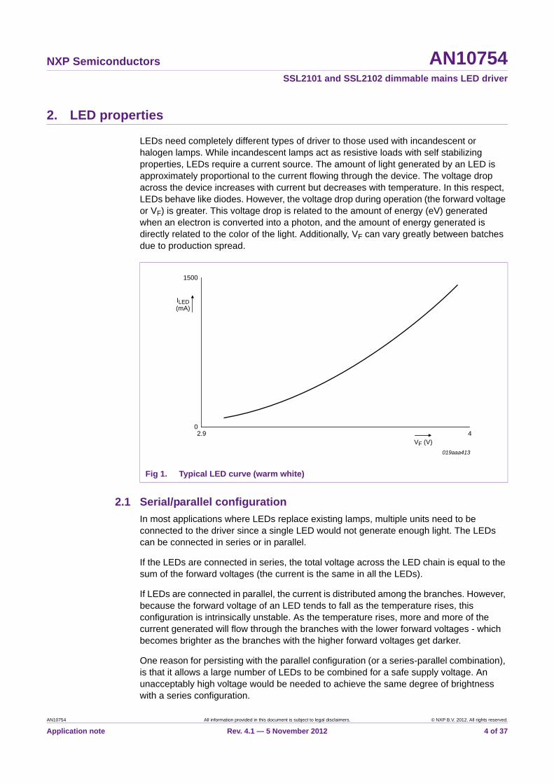
LEDs need completely different types of driver to those used with incandescent or halogen lamps. While incandescent lamps act as resistive loads with self stabilizing properties, LEDs require a current source. The amount of light generated by an LED is approximately proportional to the current flowing through the device. The voltage drop across the device increases with current but decreases with temperature. In this respect, LEDs behave like diodes. However, the voltage drop during operation (the forward voltage or VF) is greater. This voltage drop is related to the amount of energy (eV) generated when an electron is converted into a photon, and the amount of energy generated is directly related to the color of the light. Additionally, VF can vary greatly between batches due to production spread.
2.1 Serial/parallel configuration
In most applications where LEDs replace existing lamps, multiple units need to be connected to the driver since a single LED would not generate enough light. The LEDs can be connected in series or in parallel.
If the LEDs are connected in series, the total voltage across the LED chain is equal to the sum of the forward voltages (the current is the same in all the LEDs).
If LEDs are connected in parallel, the current is distributed among the branches. However, because the forward voltage of an LED tends to fall as the temperature rises, this configuration is intrinsically unstable. As the temperature rises, more and more of the current generated will flow through the branches with the lower forward voltages - which becomes brighter as the branches with the higher forward voltages get darker.
One reason for persisting with the parallel configuration (or a series-parallel combination), is that it allows a large number of LEDs to be combined for a safe supply voltage. An unacceptably high voltage would be needed to achieve the same degree of brightness with a series configuration.
Fig 1. Typical LED curve (warm white)
019aaa413
VF (V)2.9 4
1500
ILED(mA)
0
AN10754 All information provided in this document is subject to legal disclaimers. © NXP B.V. 2012. All rights reserved.
Application note Rev. 4.1 — 5 November 2012 4 of 37
NXP Semiconductors AN10754SSL2101 and SSL2102 dimmable mains LED driver
The parallel configuration also offers the advantage of redundancy. If a single LED or connection in a series-connected LED chain fails, resulting in an open circuit, the light will go out in all the LEDs in the chain. This would not happen if the LEDs were connected in parallel. With a parallel configuration, it is recommended that current regulation be added at each branch to prevent thermal runaway and the unequal distribution of current and light. In general, power converters operate at optimal efficiency when the difference between output and input voltages is minimized. With mains powered drivers and LEDs, optimizing this aspect will generate higher output voltages, allowing more LEDs to be connected in series.
AN10754 All information provided in this document is subject to legal disclaimers. © NXP B.V. 2012. All rights reserved.
Application note Rev. 4.1 — 5 November 2012 5 of 37
NXP Semiconductors AN10754SSL2101 and SSL2102 dimmable mains LED driver
3. Flyback converter basics
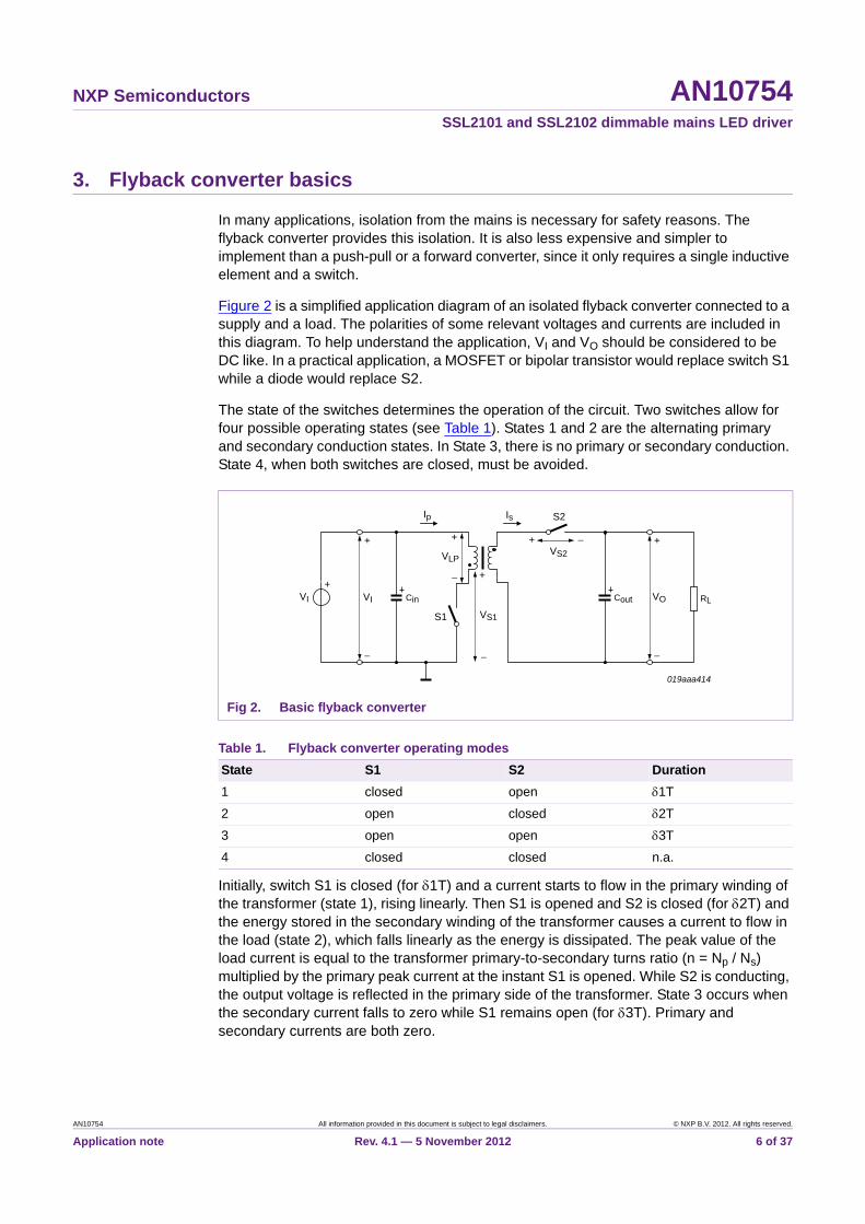
In many applications, isolation from the mains is necessary for safety reasons. The flyback converter provides this isolation. It is also less expensive and simpler to implement than a push-pull or a forward converter, since it only requires a single inductive element and a switch.
Figure 2 is a simplified application diagram of an isolated flyback converter connected to a supply and a load. The polarities of some relevant voltages and currents are included in this diagram. To help understand the application, VI and VO should be considered to be DC like. In a practical application, a MOSFET or bipolar transistor would replace switch S1 while a diode would replace S2.
The state of the switches determines the operation of the circuit. Two switches allow for four possible operating states (see Table 1). States 1 and 2 are the alternating primary and secondary conduction states. In State 3, there is no primary or secondary conduction. State 4, when both switches are closed, must be avoided.
Initially, switch S1 is closed (for 1T) and a current starts to flow in the primary winding of the transformer (state 1), rising linearly. Then S1 is opened and S2 is closed (for 2T) and the energy stored in the secondary winding of the transformer causes a current to flow in the load (state 2), which falls linearly as the energy is dissipated. The peak value of the load current is equal to the transformer primary-to-secondary turns ratio (n = Np / Ns) multiplied by the primary peak current at the instant S1 is opened. While S2 is conducting, the output voltage is reflected in the primary side of the transformer. State 3 occurs when the secondary current falls to zero while S1 remains open (for 3T). Primary and secondary currents are both zero.
Fig 2. Basic flyback converter
Table 1. Flyback converter operating modes
State S1 S2 Duration
1 closed open 1T
2 open closed 2T
3 open open 3T
4 closed closed n.a.
Ip Is S2
VI VI Cin Cout RL
VS2
VO
VS1S1
019aaa414
++
+ +
−
+
−−
VLP
+
−
−
AN10754 All information provided in this document is subject to legal disclaimers. © NXP B.V. 2012. All rights reserved.
Application note Rev. 4.1 — 5 November 2012 6 of 37

NXP Semiconductors AN10754SSL2101 and SSL2102 dimmable mains LED driver
In this mode of operation, where the primary conducts for 1T (the primary stroke), the secondary conducts for 2T (the secondary stroke) after which conduction is halted for 3T. This is referred to as Discontinuous Conduction Mode (DCM). If a new cycle begins as soon as the secondary current falls to zero (3T = 0), the converter is operating in Boundary Conduction Mode (BCM).
Figure 3 shows the equivalent circuit diagrams for the three valid states when a converter is operating in DCM mode. Simplified waveforms for one complete switching cycle are also shown.
More detailed discussions of the operation of flyback converters can be found in electronic engineering reference books.
Fig 3. Flyback equivalent circuits and waveforms (DCM mode)
�� ��
��
���
���
���
��� � ��
���
���
�
��
���
����
���������
�
�
����������
�
����
�
��
��
�� ��� � ��� ���
��
���
�
��
�� ��� � ��
���
� ���
��
����
�
��
��
�
��
�
�
��������
��
��
��
��
���
��
��������
����� �
����� ��
!"
��������!"����#��$����%��
���������!�"����%�&��$����%��
������'��!'"�
��%��&
%���
!�"
%���
��%��&
!'"
!" !�" !'"
%���
%���
�
�
�
AN10754 All information provided in this document is subject to legal disclaimers. © NXP B.V. 2012. All rights reserved.
Application note Rev. 4.1 — 5 November 2012 7 of 37

NXP Semiconductors AN10754SSL2101 and SSL2102 dimmable mains LED driver
4. Mains dimming
Standard industrial and household dimmers were designed to be used with incandescent lamps. Some of the more advanced types can be used with transformers connected to halogen lamps. LED-specific mains dimmers are still uncommon.
The cost of buying and installing a new dedicated dimmer can easily exceed that of the light source itself. So an LED system that will work with the existing dimming infrastructure, such as one that is based around the SSL2101/2102, will open up this market segment.
Existing dimmers are designed to be used with a minimum load of an incandescent lamp (which approximates a resistive load of at least 20 W and 50 W) and require additional circuitry to allow them to be used in an LED system. There is no standard for incandescent dimmers which, in practice, leads to a large spread in performance and parameter values.
4.1 Dimmer switch classification
Dimmer switches work by turning off power to the lighting circuit during part of the supply cycle. By rapidly (twice for each cycle of the supply voltage, or 100 to 120 times per second) turning the light circuit on and off, the total energy delivered to the lighting element is reduced. The longer the power is off during each cycle, the dimmer the light becomes. The thermal persistence of the filament smooths out the pulses, ensuring flickering due to the rapid switching is imperceptible.
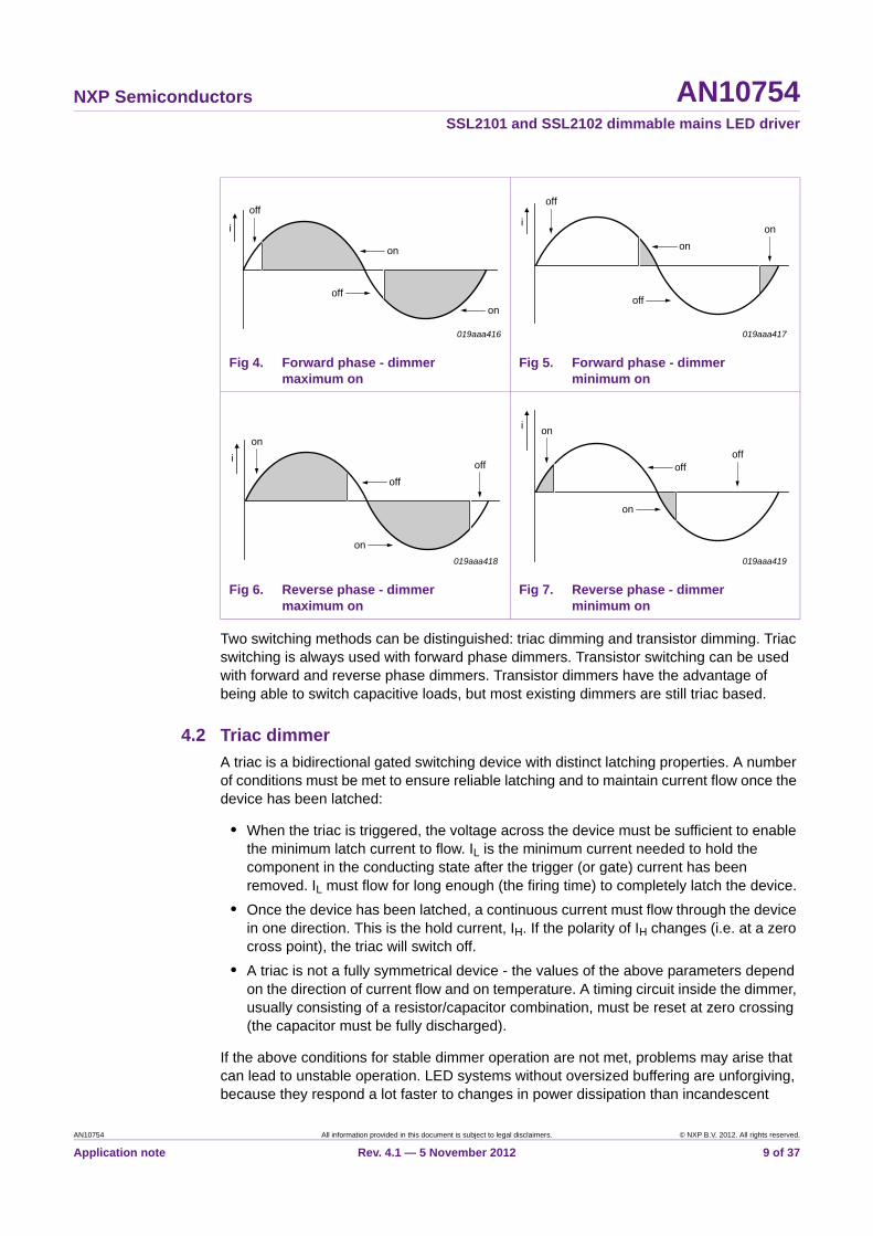
Dimmers can be divided into two operational categories: positive angle/forward phase operation, also known leading edge dimming, and negative angle/reverse phase operation, or trailing edge dimming.
Forward phase dimmers work by varying the switch ON point of the supply current to a lighting circuit. They detect the start (zero-crossing point) of each half-cycle of the supply voltage, then wait for a predetermined period before switching on the current.
Reverse phase dimmers vary the switch OFF point, cutting off the supply current to the lighting circuit at predetermined intervals.
AN10754 All information provided in this document is subject to legal disclaimers. © NXP B.V. 2012. All rights reserved.
Application note Rev. 4.1 — 5 November 2012 8 of 37
NXP Semiconductors AN10754SSL2101 and SSL2102 dimmable mains LED driver
Two switching methods can be distinguished: triac dimming and transistor dimming. Triac switching is always used with forward phase dimmers. Transistor switching can be used with forward and reverse phase dimmers. Transistor dimmers have the advantage of being able to switch capacitive loads, but most existing dimmers are still triac based.
4.2 Triac dimmer
A triac is a bidirectional gated switching device with distinct latching properties. A number of conditions must be met to ensure reliable latching and to maintain current flow once the device has been latched:
• When the triac is triggered, the voltage across the device must be sufficient to enable the minimum latch current to flow. IL is the minimum current needed to hold the component in the conducting state after the trigger (or gate) current has been removed. IL must flow for long enough (the firing time) to completely latch the device.
• Once the device has been latched, a continuous current must flow through the device in one direction. This is the hold current, IH. If the polarity of IH changes (i.e. at a zero cross point), the triac will switch off.
• A triac is not a fully symmetrical device - the values of the above parameters depend on the direction of current flow and on temperature. A timing circuit inside the dimmer, usually consisting of a resistor/capacitor combination, must be reset at zero crossing (the capacitor must be fully discharged).
If the above conditions for stable dimmer operation are not met, problems may arise that can lead to unstable operation. LED systems without oversized buffering are unforgiving, because they respond a lot faster to changes in power dissipation than incandescent
Fig 4. Forward phase - dimmer maximum on
Fig 5. Forward phase - dimmer minimum on
Fig 6. Reverse phase - dimmer maximum on
Fig 7. Reverse phase - dimmer minimum on
019aaa416
on
off
off
on
i
019aaa417
ion
on
off
off
019aaa418
off
on
on
offi
019aaa419
i on
off
on
off
AN10754 All information provided in this document is subject to legal disclaimers. © NXP B.V. 2012. All rights reserved.
Application note Rev. 4.1 — 5 November 2012 9 of 37

NXP Semiconductors AN10754SSL2101 and SSL2102 dimmable mains LED driver
lamps. Even small variations in light output in the response frequency of the human eye (200 Hz to 120 Hz) can cause flickering and be disturbing. So the switching frequency should not be allowed to fall below 200 Hz. It should be noted that the human eye is more susceptible to variations in color than brightness.
4.3 Transistor dimmer
A transistor dimmer uses a rectifier bridge in combination with a switching device such as a MOSFET or bipolar transistor to switch the main current. It contains additional circuitry to drive these devices, and this circuitry needs to be powered. The power is tapped from the switch while it is open, and stored in a capacitor. Though the energy dissipated in the dimmer electronics is not substantial, the current drawn over the switch can be a lot greater than the current required for a passive timing circuit.
AN10754 All information provided in this document is subject to legal disclaimers. © NXP B.V. 2012. All rights reserved.
Application note Rev. 4.1 — 5 November 2012 10 of 37
NXP Semiconductors AN10754SSL2101 and SSL2102 dimmable mains LED driver
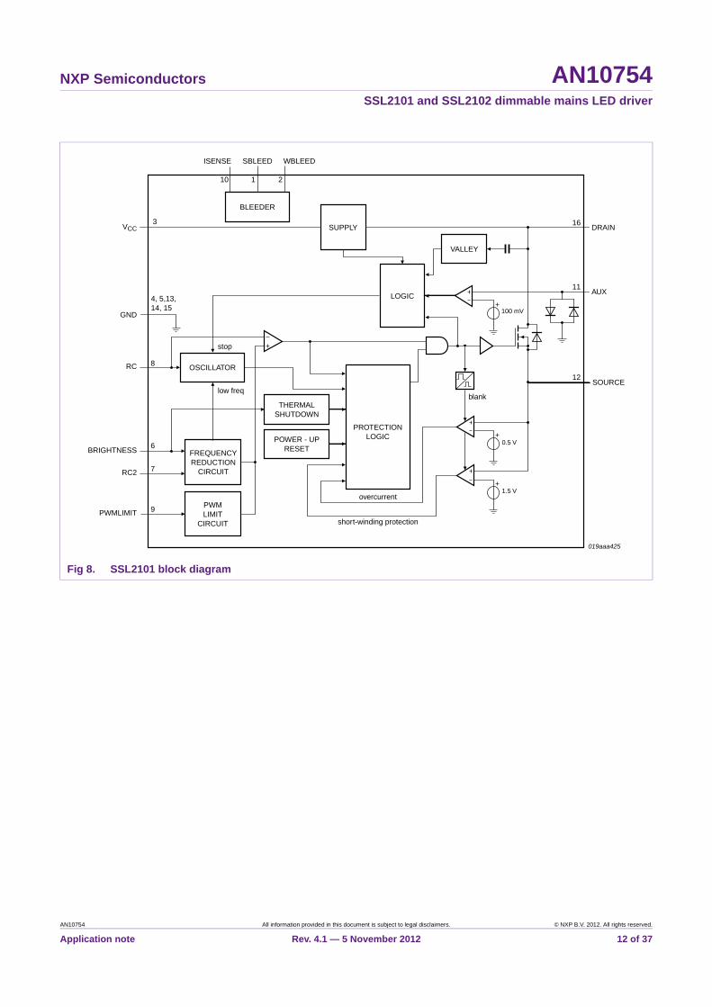
5. Functional description
The SSL2101 is a Multi-Chip Module (MCM) in an SO16 package, whilst the SSL2102 has a SO20W package. They both contains the same efficient power converter and internal circuitry to achieve mains dimmer compatibility. They have the following advantages over existing solutions:
• Integrated power switch. This reduces component costs and also ensures optimal drive and switch protection.
• Valley detection. This feature reduces converter losses, because the switch is closed at the optimal time.
• Integrated bleeder switches and comparator. This reduces component count and size.
• Smart bleeder operation. The IC senses when bleeder action is not required (e.g. the LED chain provides sufficient load). This reduces power dissipation and increases system efficiency.
• Enhanced thermal lead frame. This can increase the lifetime of the IC and enable it to operate at higher ambient temperatures. In retrofit solutions, the lifetime of electronics at elevated temperatures can be a critical parameter.
• Dimming by duty factor control and by converter frequency. This allows the designer more freedom to define parameter values. More accurate control of low dim levels can be achieved, and audible transformer noise eliminated, by adjusting the parameters controlling both dimming systems.
• Logarithmic dimming correction. This enables the dimming behavior of the LEDs to replicate that of an incandescent or halogen lamp.
• Built-in thermal protection, overcurrent protection, short-winding detection and maximum duty factor limiting. These features ensure the reliable operation of the IC with minimum failures, even when operating outside specifications.
Further details and full specifications can be found in the SSL2101/2102 data sheets (Ref. 1 and Ref. 2).
AN10754 All information provided in this document is subject to legal disclaimers. © NXP B.V. 2012. All rights reserved.
Application note Rev. 4.1 — 5 November 2012 11 of 37
NXP Semiconductors AN10754SSL2101 and SSL2102 dimmable mains LED driver
Fig 8. SSL2101 block diagram
ISENSE SBLEED WBLEED
BLEEDER
SUPPLY
LOGIC
PROTECTIONLOGIC
OSCILLATOR
FREQUENCYREDUCTION
CIRCUIT
overcurrent
blanklow freq
stop
short-winding protection
THERMALSHUTDOWN
POWER - UPRESET
PWMLIMIT
CIRCUIT
VALLEY
DRAIN
AUX
SOURCE
100 mV
0.5 V
1.5 V
VCC
RC
BRIGHTNESS
RC2
PWMLIMIT
GND
019aaa425
3
4, 5,13, 14, 15
8
6
7
9
10 1 2
16
11
12
AN10754 All information provided in this document is subject to legal disclaimers. © NXP B.V. 2012. All rights reserved.
Application note Rev. 4.1 — 5 November 2012 12 of 37
NXP Semiconductors AN10754SSL2101 and SSL2102 dimmable mains LED driver
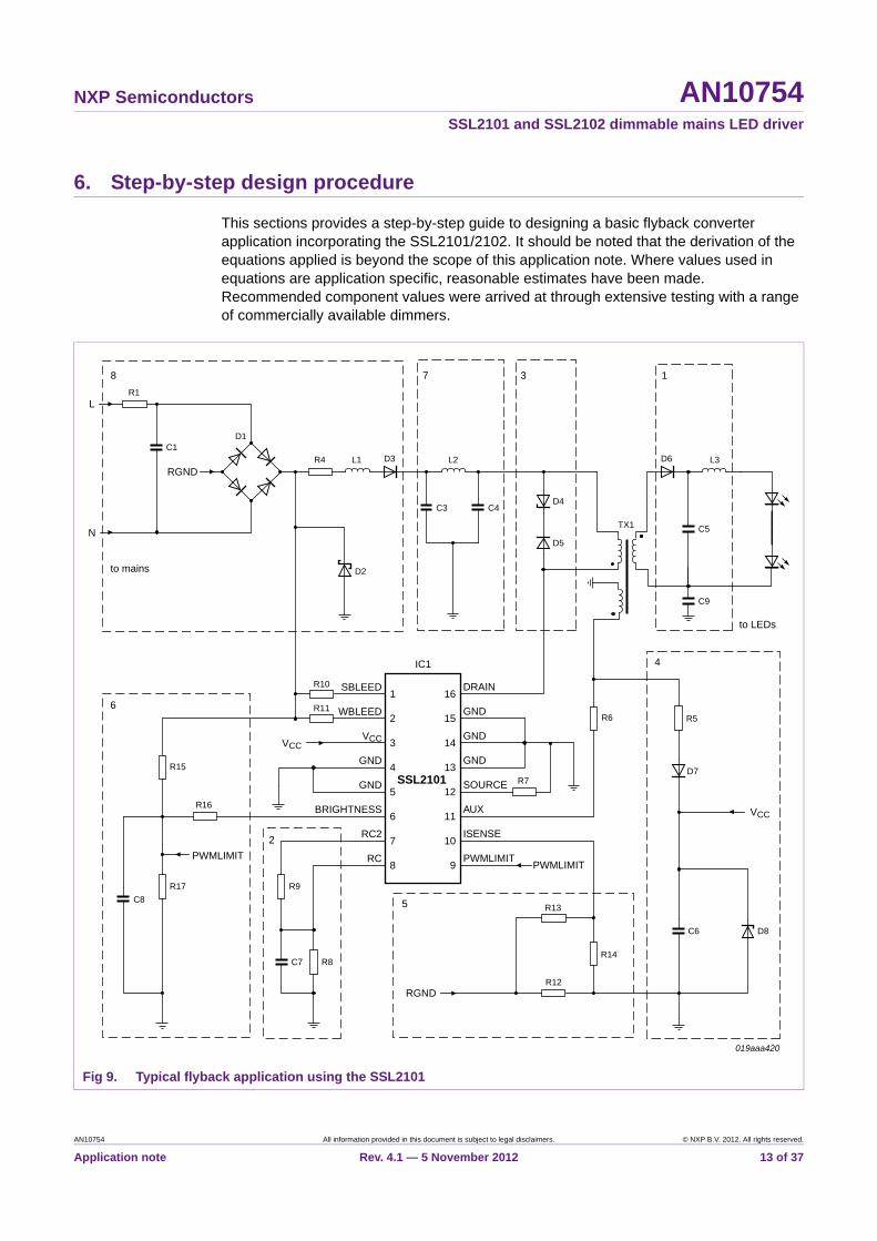
6. Step-by-step design procedure
This sections provides a step-by-step guide to designing a basic flyback converter application incorporating the SSL2101/2102. It should be noted that the derivation of the equations applied is beyond the scope of this application note. Where values used in equations are application specific, reasonable estimates have been made. Recommended component values were arrived at through extensive testing with a range of commercially available dimmers.
Fig 9. Typical flyback application using the SSL2101
SBLEED DRAIN
IC1
GND
GND
GND
SOURCE
AUX
ISENSE
PWMLIMITPWMLIMIT
to mains
to LEDs
16
15
14
13
12
11
10
9
1
2
3
4
5
6
7
8
WBLEED
VCC
GND
GND
BRIGHTNESS
RC2
RC
SSL2101
PWMLIMIT
RGND
VCC
VCC
L
N
RGND
019aaa420
R1
R4
R6
R14
R13
R16
R11
R10
R7
R15
C8
R12
R5
R8C7
R9R17
D7
C6 D8
L2 L3
C3
C5
C9
C4
L1 D3 D6
TX1
D4
D5
D2
C1D1
8
6
2
5
4
7 3 1
AN10754 All information provided in this document is subject to legal disclaimers. © NXP B.V. 2012. All rights reserved.
Application note Rev. 4.1 — 5 November 2012 13 of 37
NXP Semiconductors AN10754SSL2101 and SSL2102 dimmable mains LED driver
6.1 Basic configuration
A circuit for a typical flyback application driving a single LED chain is shown in Figure 9.
The mains voltage is rectified, buffered and filtered in the input section and connected to the primary winding of the transformer. The following functional blocks can be identified in the SSL2101/2102 application (refer to Figure 9):
1. Output circuit
2. Oscillator
3. Snubber
4. VCC generation
5. Bleeder settings
6. Dimming detection
7. Mains buffer
8. Input circuit
In the output section, the transferred energy is stored in a capacitor (C5) and filtered by inductor (L3) before driving the LED chain. A clamp is added across the primary winding of the transformer to prevent a high voltage overshoot on the DRAIN pin of the SSL2101/2102, at the moment the internal power MOSFET is switched off. A dimming detection circuit divides and filters the mains rectified voltage to provide input for the generation of the dimming curve.
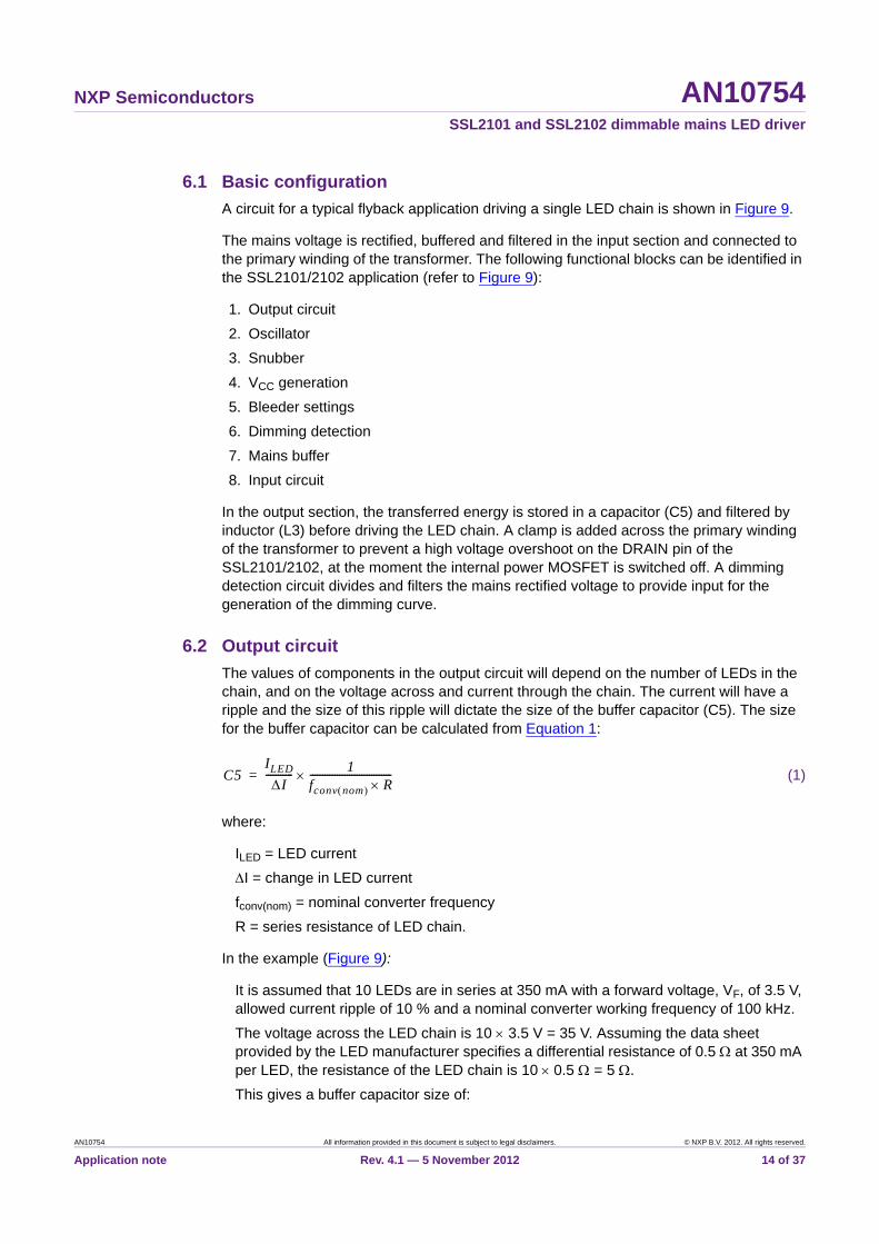
6.2 Output circuit
The values of components in the output circuit will depend on the number of LEDs in the chain, and on the voltage across and current through the chain. The current will have a ripple and the size of this ripple will dictate the size of the buffer capacitor (C5). The size for the buffer capacitor can be calculated from Equation 1:
(1)
where:
ILED = LED current
I = change in LED current
fconv(nom) = nominal converter frequency
R = series resistance of LED chain.
In the example (Figure 9):
It is assumed that 10 LEDs are in series at 350 mA with a forward voltage, VF, of 3.5 V, allowed current ripple of 10 % and a nominal converter working frequency of 100 kHz.
The voltage across the LED chain is 10 3.5 V = 35 V. Assuming the data sheet provided by the LED manufacturer specifies a differential resistance of 0.5 at 350 mA per LED, the resistance of the LED chain is 10 0.5 = 5 .
This gives a buffer capacitor size of:
C5ILED
I----------- 1
fconv nom R---------------------------------=
AN10754 All information provided in this document is subject to legal disclaimers. © NXP B.V. 2012. All rights reserved.
Application note Rev. 4.1 — 5 November 2012 14 of 37
NXP Semiconductors AN10754SSL2101 and SSL2102 dimmable mains LED driver
(2)
When using an electrolytic capacitor for C5, it is recommended that a low ESR ceramic or foil capacitor be connected in parallel to improve EMC filtering and reduce dissipation. This capacitor should be mounted closer to D6 than the electrolytic capacitor, C5.
The output coil (L3) filters the high frequency signals from the converter. The size of this coil depends of the EMC norm to be applied on the final product and on the construction, grounding and screening. As a guideline, the cut-off frequency of the LR filter (consisting of the inductance of L3 and the resistance of the LED chain) can be chosen to be 1⁄20 of the converter frequency. The coil value can be calculated using Equation 3:
(3)
Example:
This will gives an output coil value of:
(4)
Diode D6 must meet the following selection criteria:
• Be able to withstand the peak current
• Be able to withstand the maximum reverse voltage
• Have a low voltage drop in forward mode
• Have a low capacitance value in reverse mode
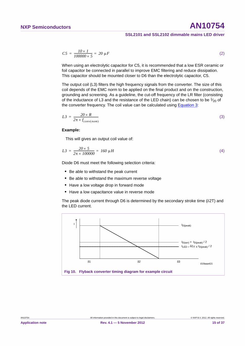
The peak diode current through D6 is determined by the secondary stroke time (2T) and the LED current.
Fig 10. Flyback converter timing diagram for example circuit
C510 1
100000 5--------------------------- 20 F==
L3 20 R2 fconv nom ------------------------------------=
L320 5
2 100000------------------------------ 160 H==
δ1 δ3δ2019aaa421
I
ILED = δ2/T X ID(peak) / 2
ID(avr) = ID(peak) / 2
ID(peak)
AN10754 All information provided in this document is subject to legal disclaimers. © NXP B.V. 2012. All rights reserved.
Application note Rev. 4.1 — 5 November 2012 15 of 37
NXP Semiconductors AN10754SSL2101 and SSL2102 dimmable mains LED driver
The peak reverse voltage across D6 is determined by the primary-to-secondary turns ratio of the transformer and the maximum buffer voltage (the voltage across C3 and C4 in the mains buffer; see Figure 9). Some margin must be applied here to allow for oscillation effects.
(5)
where:
Vrev(peak) = peak reverse voltage across diode
Vbuff(max) = maximum voltage across capacitors in buffer circuit
n = transformer primary-to-secondary turns ratio
Vosc = margin applied for oscillation effects.
VO = Output voltage
D6 can be a Schottky diode with a VF of between 0.15 V and 0.4 V or a silicium diode with a VF of around 0.7 V. Note, however that Schottky diodes have a relatively low maximum reverse voltage. A suitable Schottky diode may not be available for a given application. One of the main parameters determining reverse capacitance is junction size (which is in turn related to maximum current over sizing of diode D6) which results in unnecessary losses.
C9 is connected between ground and the secondary circuit to counter capacitive coupling between primary, auxiliary and secondary windings. To have an impact, the value of this capacitor should be much greater than the value of the capacitive coupling. As a rule of thumb, a factor of 20 is recommended. So if Ccoup = 100 pF, C9 should be > 2 nF. In the example, C9 is 2.2 nF.
If safety isolation is needed, this capacitor should be able to withstand the applied voltages, as specified EN132400 (type Yn).
6.3 Oscillator components
The maximum converter frequency and the maximum oscillator frequency are determined by the primary inductance and the transformer input power (see Section 7). The transformer input power is the sum of the power dissipated in the output circuit, the auxiliary circuit and the transformer losses. Equation 6 provides this relationship:
(6)
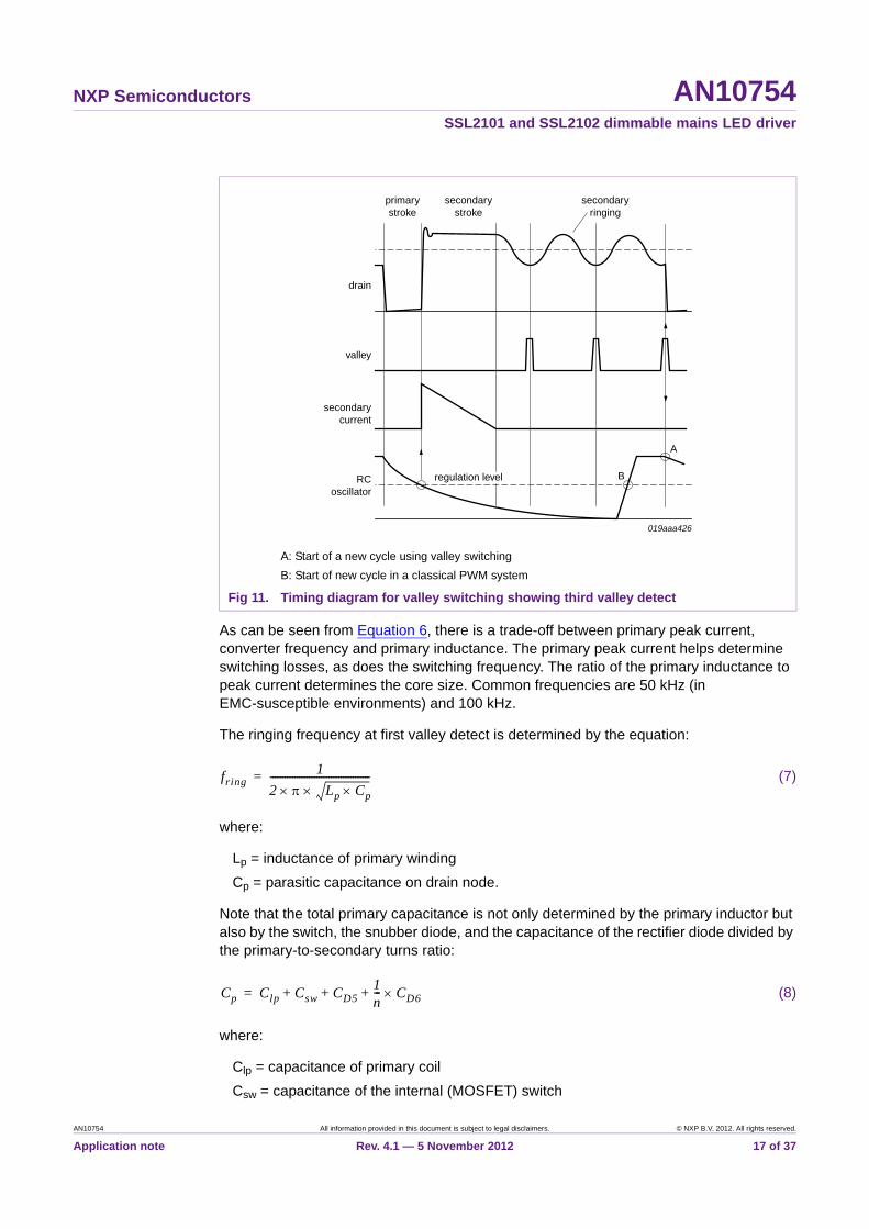
After the secondary stroke, the drain voltage oscillates at a ringing frequency, fring. The oscillator waits until it has detected a low drain voltage (a valley) before initiating a new primary stroke. For maximum efficiency, the oscillator frequency is selected to guarantee first valley detect (the first valley occurs after 1⁄2 of the period of fring). The oscillator frequency can then be lowered using the brightness input for dimming. As the oscillator frequency is lowered, valley detection is triggered at the second, third, fourth valleys, and so on - gradually increasing the off time (3T).
Vrev peak Vbuff max n VO+ Vosc+=
Lp
2 Pinput
I2p fconv
------------------------=
AN10754 All information provided in this document is subject to legal disclaimers. © NXP B.V. 2012. All rights reserved.
Application note Rev. 4.1 — 5 November 2012 16 of 37
NXP Semiconductors AN10754SSL2101 and SSL2102 dimmable mains LED driver
As can be seen from Equation 6, there is a trade-off between primary peak current, converter frequency and primary inductance. The primary peak current helps determine switching losses, as does the switching frequency. The ratio of the primary inductance to peak current determines the core size. Common frequencies are 50 kHz (in EMC-susceptible environments) and 100 kHz.
The ringing frequency at first valley detect is determined by the equation:
(7)
where:
Lp = inductance of primary winding
Cp = parasitic capacitance on drain node.
Note that the total primary capacitance is not only determined by the primary inductor but also by the switch, the snubber diode, and the capacitance of the rectifier diode divided by the primary-to-secondary turns ratio:
(8)
where:
Clp = capacitance of primary coil
Csw = capacitance of the internal (MOSFET) switch
A: Start of a new cycle using valley switching
B: Start of new cycle in a classical PWM system
Fig 11. Timing diagram for valley switching showing third valley detect
019aaa426
drain
valley
secondaryringing
secondarystroke
primarystroke
secondarycurrent
RCoscillator
regulation level
A
B
fring1
2 Lp Cp-----------------------------------------=
Cp Clp Csw CD51n--- CD6+ + +=
AN10754 All information provided in this document is subject to legal disclaimers. © NXP B.V. 2012. All rights reserved.
Application note Rev. 4.1 — 5 November 2012 17 of 37
NXP Semiconductors AN10754SSL2101 and SSL2102 dimmable mains LED driver
CD5 = capacitance of the snubber diode
CD6 = capacitance of the rectifier diode.
The time between transformer demagnetization and the first valley of fring is 1/2 of the period of the ringing frequency.
Example:
Lp = 415 H
(9)
from Equation 7:
fring = 722 kHz
This results in the first valley occurring:
(10)
after the second stroke has ended.
A nominal converter frequency of 100 kHz has a period (1T + 2T) of 10 s. This gives an actual total period (including time to first valley detect) of 10.6 s. So the actual converter frequency and the oscillator frequency, will be 94.3 kHz (fconv = fosc = 94.3 kHz).
The oscillator frequency is determined by the values of two parallel components - a resistor (R9) and a capacitor (C7). The capacitor is rapidly charged to VRC(max) (typically 2.5 V; see Ref. 1) and discharged via the resistor to VRC(min) (typical 75 mV; see Ref. 1). The discharge time has been calculated at 3.5 RC seconds (RC being the oscillator time constant). The oscillator time constant for our example can be calculated using Equation 11:
(11)
The oscillator charge time is derived from the SSL2101/2102 specification (tch(RC) = 1 s; see Ref. 1 and Ref. 2). The values for both R9 and C7 can now easily be extracted from the RC time constant.
Using an oscillator capacitor of less than 220 pF is not recommended. The drain voltage might distort the oscillator voltage in this situation. From an efficiency point of view, a value for C7 of less than 1 nF is preferred.
Example:
From Equation 11, a switching frequency of 94.3 kHz would require an oscillator time constant of 2.74 s. This time constant can be achieved by connecting a 4.0 k resistor (R9) and a 680 pF capacitor (C7) in parallel.
Cp 20 70 101
1.2------- 20 117 pF=+ + +=
T 12 fring------------------- 0.6 s= =
RC1
3.5------- 1
fosc-------- tRC ch – =
AN10754 All information provided in this document is subject to legal disclaimers. © NXP B.V. 2012. All rights reserved.
Application note Rev. 4.1 — 5 November 2012 18 of 37
NXP Semiconductors AN10754SSL2101 and SSL2102 dimmable mains LED driver
Dimming can be implemented by lowering the oscillator frequency. The frequency reduction range is determined by the ratio of R8 to R9. Due to timing tolerance issues, it is recommended that R8 should not be greater than 220 k.
Example:
For a dimming range between 100 % and 5 %, the frequency range is from 94.3 kHz down to 4.8 kHz (maximum dimming). Again applying Equation 11, at a switching frequency of 4.8 kHz, R8 is 87 k. The nearest standard value is 91 k.
6.4 Snubber circuit design
The snubber circuit (block 3 in Figure 9) uses a combination of a blocking diode (D5) and a Zener diode (D4). This approach is more efficient (lower losses) than alternative designs in the applied power range (see Table 2).
The maximum clamping voltage can be calculated using Equation 12:
(12)
where:
Vzener = the breakdown voltage of the SSL2101/2102 integrated power MOSFET
VDRAIN(max) = maximum drain voltage = 600 V (see Ref. 1).
Since the power MOSFET is not avalanche rugged, a small safety margin of 25 V is included.
Example:
At a maximum buffer voltage of 384 V and a maximum drain voltage of 600 V, from Equation 12:
(13)
A 200 V Zener diode was selected for D4.
6.5 VCC generation
A circuit consisting of a capacitor, a rectifier diode, a peak current limiting resistor and a protection Zener diode is used to generate an external VCC supply for the IC (see block 4 in Figure 9). The choice of component values involves a delicate trade-off between power dissipation and operation.
The values are determined by the output voltage, the transformer auxiliary-to-secondary turns ratio, the VCC current and the lowest converter frequency: VCC should be between 10.75 V (VCC(startup)(max); see Ref. 1) and 40 V and the current should be 2 mA. A value is required for the Zener diode, that ensures sufficient energy is stored in the buffering
Table 2. Flyback converter operating modes
Method Power range Efficiency (% losses)
RC snubber PO < 3 W 20 %
RCD clamp full range 15 %
Zener clamp full range 10 %
Vzener VDRAIN max Vbuff max 25––=
Vzener 600 384– 25 191 V=–=
AN10754 All information provided in this document is subject to legal disclaimers. © NXP B.V. 2012. All rights reserved.
Application note Rev. 4.1 — 5 November 2012 19 of 37
NXP Semiconductors AN10754SSL2101 and SSL2102 dimmable mains LED driver
capacitor without exceeding VCC. 30 V at 500 mW would be a practical value. The maximum dissipation is determined by the current delivered to the VCC circuit at the highest converter frequency.
The auxiliary-to-secondary turns ratio can be calculated using Equation 14:
(14)
where:
m = auxiliary-to-secondary turns ratio
Na = the number of turns in the auxiliary winding
Ns = the number of turns in the secondary winding
Vaux = the voltage generated across the auxiliary winding
VD6 = the voltage across D6 when it is conducting (normally between 0.3 V and 0.8 V)
Vled = the voltage across the LED chain.
The value of R5 can be calculated using the following equation:
(15)
where:
fmin = the minimum converter frequency during dimming
fmax = the maximum converter frequency during dimming
1min = the minimum primary stroke duty factor at deepest dimming
1nom = the nominal primary stroke duty factor
VCC(min) = the nominal minimum value for VCC (> VCC(startup)(max) - see Ref. 1)
IVCC = the minimum current to be delivered to the IC to ensure reliable operation.
D7 should be selected to withstand the peak current and reverse voltage, and the switching speed should be sufficient to operate at the converter working frequency.
The reverse voltage depends on the primary-to-auxiliary turns ratio, the maximum buffer voltage and the maximum VCC voltage (which is equal to the Zener voltage of D8).
(16)
The maximum current through D7 is limited and can be calculated at start-up by dividing Vaux by the value of R5.
Capacitor C6 should provide sufficient buffering at the lowest frequency. This can be approximated with a linear model:
(17)
mNa
Ns------
Vaux
Vled VD6+--------------------------= =
R5 2fmin
fmax----------
1min
1nom--------------
VCC min VD7– IVCC
------------------------------------------=
VrevD7
Na Vbuff max Np
------------------------------------ Vzener Vosc+ +=
C6IVCC
VCC fmin-----------------------------=
AN10754 All information provided in this document is subject to legal disclaimers. © NXP B.V. 2012. All rights reserved.
Application note Rev. 4.1 — 5 November 2012 20 of 37
NXP Semiconductors AN10754SSL2101 and SSL2102 dimmable mains LED driver
Example:
Assuming a VCC ripple voltage of 100 mV, IVCC estimated at 2 mA and fmin = 4.8 kHz, from Equation 17: .
(18)
6.6 Bleeder settings
The strong bleeder is designed to provide a low ohmic load for the dimmer to reset the dimmer timer and provide latch current. Tests have shown that the reset of the dimmer timing is related to a fixed charge transfer. With the SSL2101/2102, this bleeder switches on when the voltage on the SBLEED pin falls below Vth(SBLEED), which is typically 52 V (see Ref. 1). The strong bleeder resistor R10 can be set to the value given in Table 3 to allow the system to operate with the majority of field installed dimmers.
The weak bleeder is designed to maintain the hold current through the dimmer. It switches off when the voltage on the ISENSE pin drops below Vth(low)ISENSE, typically 250 mV (see Ref. 1). It switches on again when the voltage on the ISENSE pin rises above Vth(high)ISENSE, typically 100 mV (see Ref. 1). Hysteresis is included to prevent unwanted oscillations. The weak bleeder should switch on if the input current from the bleeder to the converter drops below the hold current of the dimmer. The weak bleeder resistor R11 should conduct this RMS current. R12 is included to dampen oscillations. Table 3 shows typical values for these components with reference to the input voltage.
The ratio between R13 and R14 can be calculated using this data: Suppose a dimmer requires a minimum hold current of 10 mA, which is maintained by means of the weak bleeder switch. Switch on at 10 mA over 200 results in 2 V across R12 (or across R13 + R14). The weak bleeder switches on when the voltage on pin ISENSE (or across R14) is 100 mV. So R14 / (R13 + R14) = 100 mV / 2 V = 1 / 20, therefore:
R13 + R14 = 20 R14
R13 = (20 1) R14
R13 / 19 = R14.
IISENSE is protected by R13 and should not exceed 5 mA. The maximum peak voltage is limited to 400 V by D2, with a safety margin of 100 V. So R13 = 500 V / 5 mA = 100 k.
Therefore, R14 = 100 k / 19 = 5.3 k.
Note that all these resistors will need to be able to withstand peak power and peak voltage. R10 and R11 should be rated to withstand the voltage at which the TVS (D2) sets in. R12 should be rated to withstand the peak voltage and pulse energy at start-up. This pulse energy is listed in resistor data and can be calculated as follows:
(19)
C6 0.002 0.1 4800 4.2 F= =
Table 3. Bleeder component settings
Input voltage R10 R11 R12
120 V (AC) 1 k 15 k 100
230 V (AC) 1.5 k 27 k 200
277 V (AC) 1.5 k 27 k 220
Epulse 1 2 C3 4+ VI peak 2=
AN10754 All information provided in this document is subject to legal disclaimers. © NXP B.V. 2012. All rights reserved.
Application note Rev. 4.1 — 5 November 2012 21 of 37
NXP Semiconductors AN10754SSL2101 and SSL2102 dimmable mains LED driver
6.7 Dimming detection
The dimming reference voltage is derived from the non-buffered rectified mains voltage, and averaged using a capacitor. This voltage is input to the BRIGHTNESS and PWMLIMIT pins in the SSL2101/2102 (see Figure 9). By balancing the voltage levels at these two inputs, the peak current through the inductor is reduced before the frequency of the converter falls. This eliminates audible noise from the transformer. The BRIGHTNESS and PWMLIMIT inputs have internal current sources, to which the working point of the converter is shifted. C8 provides filtering and has a recommended default value of 4.7 F.
R7 defines the dimming curve and regulates the maximum power delivered to the LEDs. It regulates the peak current through the inductor and thus the maximum power level. It also provides overcurrent protection to the converter. This technique removes part of the dependency between the output power and the mains voltage. The built-in overcurrent protection circuit triggers at 0.52 V. If the secondary losses and frequency are known, R7 can be calculated as follows:
(20)
where:
Pin = Pin(trans) (see Section 6.3) + snubber losses.
6.8 Buffer circuit
The buffer circuit is made out of two capacitors and an inductor. The circuit has dual functionality. The first function is to store energy to ensure the converter can transfer power continuously to the LED chain. LED operation becomes independent of dimmer operation and mains power fluctuations are filtered out. The second function is to filter ripple current generated by the converter to ensure compliance with legal requirements in relation to mains conducted emissions.
To implement the first function, the voltage across the converter should not fall below the minimum working voltage within a single mains cycle. The total capacitance (C3 + C4) can be estimated as follows.
First the minimum voltage at which the converter will still deliver full power needs to be calculated. This is either a duty-factor limit of 75% or the ratio of cycle time to cycle time minus secondary stroke time and is derived from the calculated primary inductance and peak current:
(21)
Table 4. Recommended dimming circuit values
Input voltage R15 R16 R17
120 V (AC) 680 k 15 k 10 k
230 V (AC) 1.5 M 15 k 10 k
277 V (AC) 1.5 M 15 k 8.2 k
R7fconv Lp
8 pin-----------------------=
Vbuff min 1
lmax------------ fconv Ip Lp=
AN10754 All information provided in this document is subject to legal disclaimers. © NXP B.V. 2012. All rights reserved.
Application note Rev. 4.1 — 5 November 2012 22 of 37
NXP Semiconductors AN10754SSL2101 and SSL2102 dimmable mains LED driver
Next the time between the peak voltage and when the mains voltage has reached this minimum voltage needs to be calculated. Allow a margin of 10 V to allow for voltage drop during capacitor charging:
(22)
where:
fnet = frequency of mains voltage
(23)
Now take the transformer input power and add IC losses and snubber losses. Equation 24 can be used to calculate the total buffer capacitance:
(24)
where
Ptot = Pin + IC losses.
The combination of L2, C3 and C4 constitute a Pi-Filter that will help to filter out the high frequency currents generated by converter action. Although a single filter stage will not be enough to satisfy legal requirements in relation to mains conducted emissions, it will go some way to achieving these goals. The cut-off frequency of this filter should be a magnitude below the converter frequency:
(25)
Assuming C3 = C4. If the cut-off frequency is selected to be a decade below the working frequency, the resulting equation for L2 becomes:
(26)
where:
Cs = C3 = C4.
It is recommended that a low-frequency absorbent soft ferrite material, like 3S1 (Ferroxcube) or 3W1200 (Würth), be used for this inductor in order to dissipate high frequency energy and block unwanted oscillations.
tdis 12--- arc
Vbuff min 10+
Vmainspeak----------------------------------- sin+
14 fnet-----------------=
Vmainspeak V AC RMS 2=
C3 C4+2 Ptot tdis
Vmainspeak2
Vbuff min 2
–------------------------------------------------------------=
fcutoff1
2 L2C3 C4C3 C4+---------------------
--------------------------------------------------------=
L2 100
Cs 42 fconv2
------------------------------------------=
AN10754 All information provided in this document is subject to legal disclaimers. © NXP B.V. 2012. All rights reserved.
Application note Rev. 4.1 — 5 November 2012 23 of 37
NXP Semiconductors AN10754SSL2101 and SSL2102 dimmable mains LED driver
6.9 Input circuit
The input circuit rectifies the mains voltage and provides overcurrent and overvoltage protection. It has to be over-dimensioned to cope with overvoltage and overcurrent conditions on the input. Primary protection consists of a fuse or fusistor that breaks down when the current exceeds a specified value. If a fuse is used, a breakdown value should be selected that can handle inrush currents whilst still providing overcurrent protection. In practice, a value of between 1 A and 1.5 A is sufficient. If a fusistor is selected, the minimum value for this resistor can be calculated using Equation 27. For almost all diode bridge rectifiers, the IFSM parameter is around 20 A.
(27)
Example:
For a supply of 230 V (AC) 20 % and VAC(max) = 276 V, R1 = 19.5 . The nearest E24 series standard value is 20 .
Besides its ohmic value, the continuous power dissipation in R1 is an important characteristic. This value can be determined using Equation 28:
(28)
where:
the crest factor is the ratio of RMS to average current, typically 4.
Example:
For a supply of 230 V (AC), Ptot = 15.7 W (see Section 6.8), R1 = 20 and crest factor = 4, the power dissipated in R1 is 370 mW.
Capacitor C1 is added to improve differential mode filtering. By placing this component close to the mains input, the inductive coupling to mains is reduced. It also provides buffering against voltage spikes. The values of these input components are partly determined by the requirements of the dimmer. At low levels of output power, R4 can be added to reduce the audible noise generated by inrush current towards C3 / C4.
Components D1 and D3 should be dimensioned to handle the peak current in the circuit. This peak current is restricted by the combination of R12, R1 and R4.
(29)
Example:
For a supply of 230 V (AC) 20 %, R12 = 260 , R1 = 20 and R4 = 0 , the peak current is 1.4 A.
R12 VAC max
IFSM-----------------------------------=
PR1 Ccrestfactor R1Ptot
2
VAC2
------------=
Ipeak
2 VAC max R12 R1 R4+ +------------------------------------=
AN10754 All information provided in this document is subject to legal disclaimers. © NXP B.V. 2012. All rights reserved.
Application note Rev. 4.1 — 5 November 2012 24 of 37
NXP Semiconductors AN10754SSL2101 and SSL2102 dimmable mains LED driver
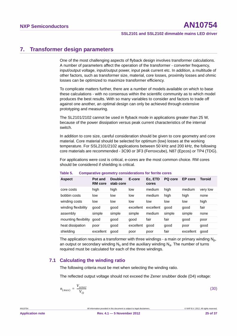
7. Transformer design parameters
One of the most challenging aspects of flyback design involves transformer calculations. A number of parameters affect the operation of the transformer - converter frequency, input/output voltage, input/output power, input peak current etc. In addition, a multitude of other factors, such as transformer size, material, core losses, proximity losses and ohmic losses can be optimized to maximize transformer efficiency.
To complicate matters further, there are a number of models available on which to base these calculations - with no consensus within the scientific community as to which model produces the best results. With so many variables to consider and factors to trade off against one another, an optimal design can only be achieved through extensive prototyping and measuring.
The SL2101/2102 cannot be used in flyback mode in applications greater than 25 W, because of the power dissipation versus peak current characteristics of the internal switch.
In addition to core size, careful consideration should be given to core geometry and core material. Core material should be selected for optimum (low) losses at the working temperature. For SSL2101/2102 applications between 50 kHz and 200 kHz, the following core materials are recommended - 3C90 or 3F3 (Ferroxcube), N87 (Epcos) or TP4 (TDG).
For applications were cost is critical, e-cores are the most common choice. RM cores should be considered if shielding is critical.
The application requires a transformer with three windings - a main or primary winding Np, an output or secondary winding Ns and the auxiliary winding Na. The number of turns required must be calculated for each of the three windings.
7.1 Calculating the winding ratio
The following criteria must be met when selecting the winding ratio.
The reflected output voltage should not exceed the Zener snubber diode (D4) voltage:
(30)
Table 5. Comparative geometry considerations for ferrite cores
Aspect Pot and RM core
Double stab core
E-core Ec, ETD cores
PQ core EP core Toroid
core costs high high low medium high medium very low
bobbin costs low low low medium high high none
winding costs low low low low low low high
winding flexibility good good excellent excellent good good fair
assembly simple simple simple medium simple simple none
mounting flexibility good good good fair fair good poor
heat dissipation poor good excellent good good poor good
shielding excellent good poor poor fair excellent good
n max Vzener
VO---------------=
AN10754 All information provided in this document is subject to legal disclaimers. © NXP B.V. 2012. All rights reserved.
Application note Rev. 4.1 — 5 November 2012 25 of 37
NXP Semiconductors AN10754SSL2101 and SSL2102 dimmable mains LED driver
Example:
Using Equation 30, if Vzener = 200 V and VO = 35 V this will result in n(max) = 5.7.
The turn ratio is calculated with an empirical equation, and the result is limited by n(max).
(31)
Example:
Using Equation 31, a value of VO = 35 V will result in n = 3.01 (less than n(max) = 5.7).
Remark: Equation 31 takes into account the wide operating area of input voltage and the fixed current output properties. A different calculation of flyback ratio is preferable for voltage to voltage converters and non-mains dimmable designs.
7.2 Calculating the primary inductance
A. To determine the primary inductance, the duty cycle at which the IC switch dissipation is acceptable needs to be calculated:
(32)
Example:
fconv = 85 kHz, fring = 303 kHz, Vbuff(avr) = (310+220) / 2 = 265 V, ILED = 350 mA, Pin = 14 W, n = 3.01. 1 = 26.8 %.
After this the next steps can be done:
B: Calculate 2:
(33)
Example:
With fring = 303 kHz, 1 = 0.268 and fconv = 85 kHz, t2 becomes 7 S. 2 = 59 %.
C: Calculating the secondary and primary peak current:
(34)
(35)
Example:
ILED = 350 mA, Is(peak) = 0.7 / 0.59 = 1.186 A, Ip(peak) = 0.394 A.
n 43.417 VO
34---–
=
1
1fconv
2 fring-------------------–
1Vbuff avr ILED
Pin n----------------------------------------+
-------------------------------------------------=
2 T t21 1–
fconv-------------- 1
2 fring-------------------–= =
Is
2 ILED2
--------------------=
IpIs
n---=
AN10754 All information provided in this document is subject to legal disclaimers. © NXP B.V. 2012. All rights reserved.
Application note Rev. 4.1 — 5 November 2012 26 of 37
NXP Semiconductors AN10754SSL2101 and SSL2102 dimmable mains LED driver
D: Calculating primary inductance:
(36)
Example:
Pin = 14 W, fconv = 85 kHz, Lp = 2.1 mH.
E: Recalculating the ringing frequency:
(37)
Example:
Lp = 2.1 mH, Cp = 110 pF, fring = 303 kHz.
Remark: This is a circular calculation and steps A to E must be repeated with each time a new ringing frequency until the deviation from the previous calculation is small enough.
The ohmic loss in the switch can then be calculated as shown in Equation 38:
(38)
Example:
RDSon = 6.5 , Pin(trans) = 14 W, 1 = 26.5 %, Vbuff(eff) = 289 V. Psw is 115 mW.
Remark: Equation 38 not only dictates the primary inductance but also shows the relationship between primary current and power:
(39)
Example:
Vbuff = 265 V, Pinput = 14 W, fconv = 85 kHz, 1 =26.8 %, Lprim = 2.1 mH, Iprim = 0.394 A.
Remark: The initial calculation of primary duty factor was based upon minimizing the RDSon switch losses.This equation is also used in the calculation tool. It might be beneficial to reduce primary duty factor thus creating higher IC losses but lower transformer losses and better output current stabilization/input voltage variation rejection. Assuming this is applied to the limit, the minimum duty factor can be calculated using next equation:
(40)
Lp
2 Pin
Ip2
fconv------------------------=
fring1
2 Lp Cp-----------------------------------------=
Psw
2 RDSon P2in trans
V2buff eff 1
-------------------------------------------------------=
Ip
Vbuff 1Lp fconv-----------------------
2 PinputLp fconv-----------------------= =
1
2 RDSon P2in trans
V2buff eff Psw max
-------------------------------------------------------=
AN10754 All information provided in this document is subject to legal disclaimers. © NXP B.V. 2012. All rights reserved.
Application note Rev. 4.1 — 5 November 2012 27 of 37
NXP Semiconductors AN10754SSL2101 and SSL2102 dimmable mains LED driver
Example:
Assume Psw(max) (allowable RDSon switch losses) to be 0.5 W. Vbuff(eff) = 265 V, then 1 becomes 7.2 %.
A smaller 1 and larger winding ratio will lead to higher switch losses but has a number of advantages:
• It lowers primary inductance, thus reducing transformer size and losses
• In BCM, it makes the system less dependent of input voltage variation.
• In BCM, it makes the system react more to output voltage variation, which will lead to more stable LED current.
• It allows for a lower input voltage at which it still can deliver full power, thus bigger input voltage ripple and smaller input buffer capacitors.
• It allows for a lower input voltage ripple so the possibility to minimize input capacitance and increase output capacitance, which will give a high system power factor provided that the system stays in BCM mode.
Remark: It is advisable to select a primary duty factor that is between the equation as used to calculate minimum switch losses, which is also used in the calculation tool, and the above equation that utilizes the allowed switch RDSon losses.
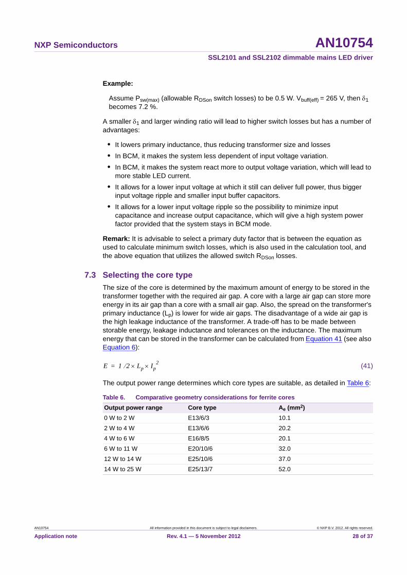
7.3 Selecting the core type
The size of the core is determined by the maximum amount of energy to be stored in the transformer together with the required air gap. A core with a large air gap can store more energy in its air gap than a core with a small air gap. Also, the spread on the transformer's primary inductance (Lp) is lower for wide air gaps. The disadvantage of a wide air gap is the high leakage inductance of the transformer. A trade-off has to be made between storable energy, leakage inductance and tolerances on the inductance. The maximum energy that can be stored in the transformer can be calculated from Equation 41 (see also Equation 6):
(41)
The output power range determines which core types are suitable, as detailed in Table 6:
Table 6. Comparative geometry considerations for ferrite cores
Output power range Core type Ae (mm2)
0 W to 2 W E13/6/3 10.1
2 W to 4 W E13/6/6 20.2
4 W to 6 W E16/8/5 20.1
6 W to 11 W E20/10/6 32.0
12 W to 14 W E25/10/6 37.0
14 W to 25 W E25/13/7 52.0
E 1 2 Lp Ip2=
AN10754 All information provided in this document is subject to legal disclaimers. © NXP B.V. 2012. All rights reserved.
Application note Rev. 4.1 — 5 November 2012 28 of 37
NXP Semiconductors AN10754SSL2101 and SSL2102 dimmable mains LED driver
7.4 Primary winding count
There is a dependency between the air gap and the number of primary turns. The air gap must be big enough to avoid tolerance issues and small enough to minimize proximity losses (caused by the fringing field). In practice, an air gap of between 100 m and 1 mm is advisable.
Equation 42 and Equation 43 can be used to establish a suitable balance between the air gap and the number of turns. The parameter Ae represents the effective core area in square meters (m2) and Bmax represents the maximum flux density in Tesla. For most ferrite materials, a Bmax value of 275 mT is low enough to prevent saturation. These values can be obtained from the core material data sheet.
The number of turns in the primary winding can be calculated using Equation 42:
(42)
The air gap can now be calculated using empirical Equation 43:
(43)
7.5 Secondary winding count
To calculate secondary windings, take the number of primary windings and divide this by winding ratio:
(44)
7.6 Auxiliary winding count
The number of windings for the transformer auxiliary output, depends on the output voltage of the converter. It can be calculated using Equation 14 as stated in Section 6.5
7.7 Selecting wire diameters
Wire diameter selection involves a trade-off between size, ohmic losses, proximity losses and skin losses. For SSL2101/2102 applications, skin losses are generally negligible for wire sizes below 0.6 mm in diameter at operating frequencies below 200 kHz. For wire diameters above 0.6 mm diameter, the use of Litze wire or multiple strands is recommended.
Ohmic losses are related to the peak currents in the wire. These can be estimated by obtaining the wire resistance, then calculating the average power dissipation. As a rule of thumb, the current density should be between 300 CM/A and 500 CM/A (Circular Mills /Amp). Table 7 gives appropriate wire sizes for a range of currents.
Np122------
Lp IpBmax Ae------------------------=
lgap M 18 Ae
9 106 Lp
Np1.9
-----------------------------
50 Ae–
----------------------------------------------------------------=
Ns
Np
n------=
AN10754 All information provided in this document is subject to legal disclaimers. © NXP B.V. 2012. All rights reserved.
Application note Rev. 4.1 — 5 November 2012 29 of 37
NXP Semiconductors AN10754SSL2101 and SSL2102 dimmable mains LED driver
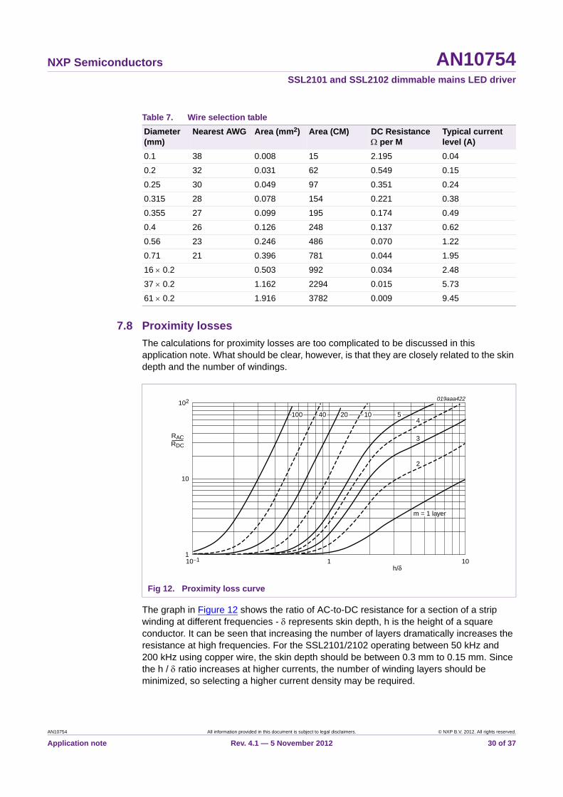
7.8 Proximity losses
The calculations for proximity losses are too complicated to be discussed in this application note. What should be clear, however, is that they are closely related to the skin depth and the number of windings.
The graph in Figure 12 shows the ratio of AC-to-DC resistance for a section of a strip winding at different frequencies - represents skin depth, h is the height of a square conductor. It can be seen that increasing the number of layers dramatically increases the resistance at high frequencies. For the SSL2101/2102 operating between 50 kHz and 200 kHz using copper wire, the skin depth should be between 0.3 mm to 0.15 mm. Since the h / ratio increases at higher currents, the number of winding layers should be minimized, so selecting a higher current density may be required.
Table 7. Wire selection table
Diameter (mm)
Nearest AWG Area (mm2) Area (CM) DC Resistance per M
Typical current level (A)
0.1 38 0.008 15 2.195 0.04
0.2 32 0.031 62 0.549 0.15
0.25 30 0.049 97 0.351 0.24
0.315 28 0.078 154 0.221 0.38
0.355 27 0.099 195 0.174 0.49
0.4 26 0.126 248 0.137 0.62
0.56 23 0.246 486 0.070 1.22
0.71 21 0.396 781 0.044 1.95
16 0.2 0.503 992 0.034 2.48
37 0.2 1.162 2294 0.015 5.73
61 0.2 1.916 3782 0.009 9.45
Fig 12. Proximity loss curve
019aaa422
h/δ10−1 101
10
102
RACRDC
1
100 40 20
m = 1 layer
2
3
410 5
AN10754 All information provided in this document is subject to legal disclaimers. © NXP B.V. 2012. All rights reserved.
Application note Rev. 4.1 — 5 November 2012 30 of 37
NXP Semiconductors AN10754SSL2101 and SSL2102 dimmable mains LED driver
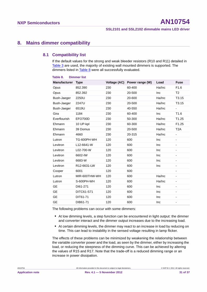
8. Mains dimmer compatibility
8.1 Compatibility list
If the default values for the strong and weak bleeder resistors (R10 and R11) detailed in Table 3 are used, the majority of existing wall mounted dimmers is supported. The dimmers listed in Table 8 were all successfully evaluated.
The following problems can occur with some dimmers:
• At low dimming levels, a step function can be encountered in light output: the dimmer and converter interact and the dimmer output increases due to the increasing load.
• At certain dimming levels, the dimmer may react to an increase in load by reducing on time. This can lead to instability in the sensed voltage resulting in lamp flicker.
The effects of these problems can be minimized by weakening the relationship between the variable converter power and the load, as seen by the dimmer, either by increasing the load, or reducing the steepness of the dimming curve. This can be achieved by altering the values of R15 and R17. Note that the trade-off is a reduced dimming range or an increase in power dissipation.
Table 8. Dimmer list
Manufacturer Type Voltage (AC) Power range (W) Load Fuse
Opus 852.390 230 60-400 Ha/Inc F1.6
Opus 852.392 230 20-500 Inc T2
Bush-Jaeger 2250U 230 20-600 Ha/Inc T3.15
Bush-Jaeger 2247U 230 20-500 Ha/Inc T3.15
Bush-Jaeger 6519U 230 40-550 Ha/Inc -
Gira 1184 230 60-400 Inc T1.6
Everflourish EFO700D 230 50-300 Ha/Inc T1.25
Ehmann 10 UP-kpl 230 60-300 Ha/Inc F1.25
Ehmann 39 Domus 230 20-500 Ha/Inc T2A
Ehmann 4660 230 20-315 Ha/Inc -
Lutron TG-600PH-WH 120 600 Inc -
Levitron L12-6641-W 120 600 Inc -
Levitron L02-700-W 120 600 Inc -
Levitron 6602-IW 120 600 Inc -
Levitron 6683-W 120 600 Inc -
Levitron R12-6631-LW 120 600 Inc -
Cooper 6001 120 600 -
Lutron MIR-600THW-WH 120 600 Ha/Inc -
Lutron S-600PH-WH 120 600 Ha/Inc -
GE DI61-271 120 600 Inc -
GE DITC61-S71 120 600 Inc -
GE DIT61-71 120 600 Inc -
GE DIB61-71 120 600 Inc -
AN10754 All information provided in this document is subject to legal disclaimers. © NXP B.V. 2012. All rights reserved.
Application note Rev. 4.1 — 5 November 2012 31 of 37
NXP Semiconductors AN10754SSL2101 and SSL2102 dimmable mains LED driver
8.2 Transistor dimmers
A transistor dimmer may demand a higher load then can be realized with the standard bleeder values, to ensure the full voltage drop when dimming is turned off. Typically, a continuous load current of 10 mA or more is required.
The dimming range is restricted with the standard dim-curve circuit, especially when deep dimming is combined with a low output load, because the average voltage drop will not be sufficient to detect dimming. To compensate for this, the dimming curve can be shifted - but the trade-off is a lower dim-range with triac dimmers. This will not be a problem as long as the output power is > 2.3 W in dimmed condition.
If the circuit needs to be compatible with both triac and transistor dimmers, and deep dimming is required at low output loads, an additional resistive bleeder can be connected in parallel with C1. A value of 22 k 3 W at 230 V (AC) or 12 k 1.5 W at 120 V (AC) would be appropriate.
A transistor dimmer with trailing edge operation does not need a hold current. Nor does it generate high inrush currents. These advantages over the standard triac dimmer can be exploited by omitting the damper network (R12/R13/R14). The ISENSE pin can be connected to GND. As a result, dissipation and audible noise is reduced during dimming, and the inrush peak current is reduced.
8.3 Multiple lamp circuits
The SSL2101/2102 ICs were both designed to operate in a one-to-one situation - one lamp connected to one dimmer. However, it is possible to connect multiple lamps to a single dimmer. There is a restriction when using leading edge triac dimmers, which is that the inrush current of all lamps must be combined, if the dimmer is to withstand these currents. Incandescent and halogen lamps can generate inrush currents several times greater than the nominal current.
The inrush current can be calculated by subtracting the buffer voltage across C3/C4 at maximum input voltage from the input voltage, and dividing this by the value of R12:
(45)
A standard value for this inrush current is 500 mA at 230 V (AC). This corresponds to a Halogen lamp of 50 W. When trailing edge dimmers are used, this inrush current is eliminated. The effective load of the lamp is close to the nominal load.
Iinrush
Vin Vbuff–
R12 R1+-------------------------=
AN10754 All information provided in this document is subject to legal disclaimers. © NXP B.V. 2012. All rights reserved.
Application note Rev. 4.1 — 5 November 2012 32 of 37
NXP Semiconductors AN10754SSL2101 and SSL2102 dimmable mains LED driver
9. Dimming curve calculations
The dimming curve describes the relationship between light output and the dimmer setting. The SSL2101/2102 both offer a great deal of freedom when selecting the dimming curve. The typical flyback application is an example of power steering: The output power dissipated in the LEDs is regulated by the IC. The current is determined by the forward voltage of the LEDs. The relationship between light output and the dimmer setting is defined in the Equation 46:
(46)
where:
= estimated converter efficiency.
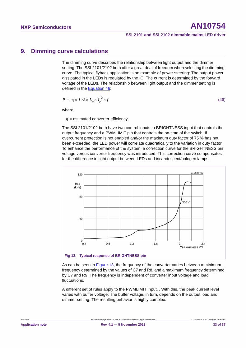
The SSL2101/2102 both have two control inputs: a BRIGHTNESS input that controls the output frequency and a PWMLIMIT pin that controls the on-time of the switch. If overcurrent protection is not enabled and/or the maximum duty factor of 75 % has not been exceeded, the LED power will correlate quadratically to the variation in duty factor. To enhance the performance of the system, a correction curve for the BRIGHTNESS pin voltage versus converter frequency was introduced. This correction curve compensates for the difference in light output between LEDs and incandescent/halogen lamps.
As can be seen in Figure 13, the frequency of the converter varies between a minimum frequency determined by the values of C7 and R8, and a maximum frequency determined by C7 and R9. The frequency is independent of converter input voltage and load fluctuations.
A different set of rules apply to the PWMLIMIT input, . With this, the peak current level varies with buffer voltage. The buffer voltage, in turn, depends on the output load and dimmer setting. The resulting behavior is highly complex.
Fig 13. Typical response of BRIGHTNESS pin
P 1 2 Lp Ip2 f=
VBRIGHTNESS (V)0.4 2.421.2 1.60.8
019aaa423
40
80
120
freq(kHz)
0
300 V
AN10754 All information provided in this document is subject to legal disclaimers. © NXP B.V. 2012. All rights reserved.
Application note Rev. 4.1 — 5 November 2012 33 of 37
NXP Semiconductors AN10754SSL2101 and SSL2102 dimmable mains LED driver
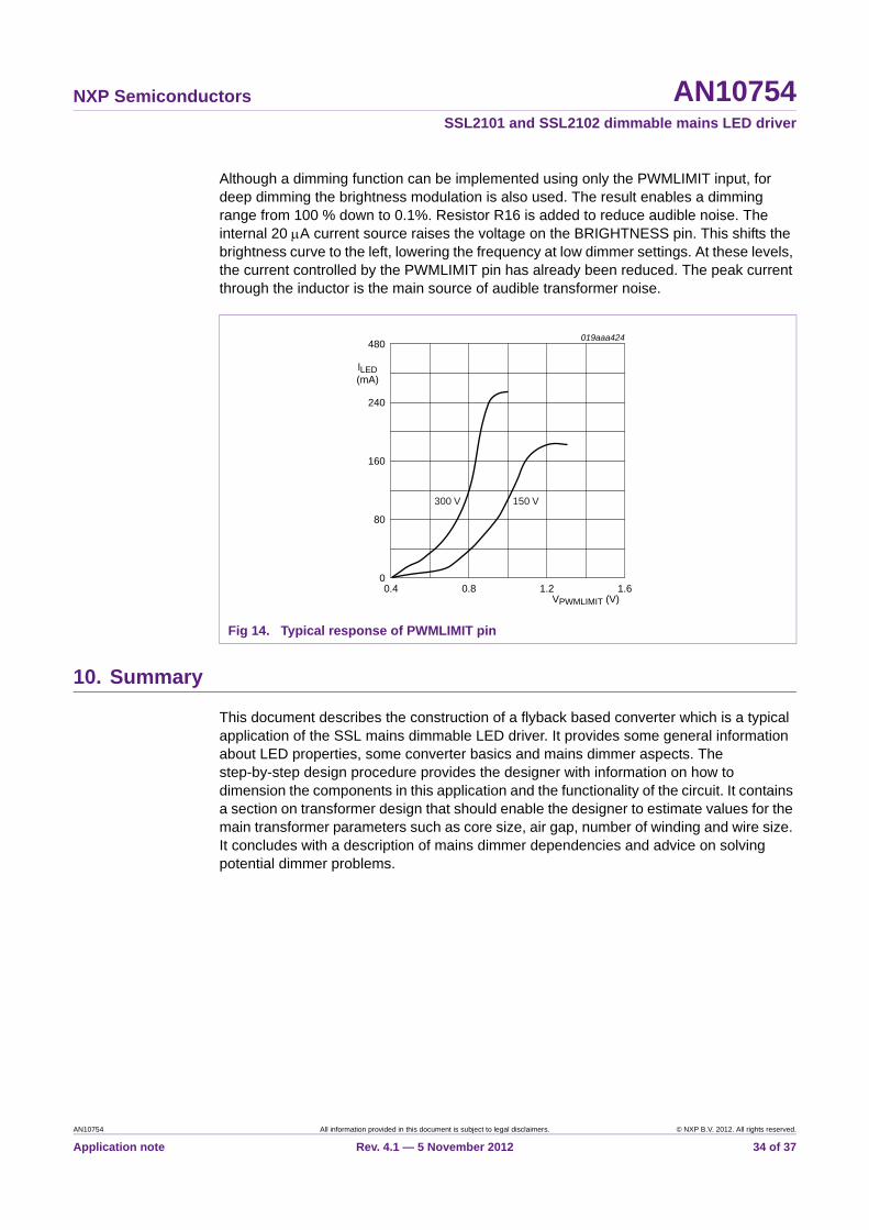
Although a dimming function can be implemented using only the PWMLIMIT input, for deep dimming the brightness modulation is also used. The result enables a dimming range from 100 % down to 0.1%. Resistor R16 is added to reduce audible noise. The internal 20 A current source raises the voltage on the BRIGHTNESS pin. This shifts the brightness curve to the left, lowering the frequency at low dimmer settings. At these levels, the current controlled by the PWMLIMIT pin has already been reduced. The peak current through the inductor is the main source of audible transformer noise.
10. Summary
This document describes the construction of a flyback based converter which is a typical application of the SSL mains dimmable LED driver. It provides some general information about LED properties, some converter basics and mains dimmer aspects. The step-by-step design procedure provides the designer with information on how to dimension the components in this application and the functionality of the circuit. It contains a section on transformer design that should enable the designer to estimate values for the main transformer parameters such as core size, air gap, number of winding and wire size. It concludes with a description of mains dimmer dependencies and advice on solving potential dimmer problems.
Fig 14. Typical response of PWMLIMIT pin
019aaa424
VPWMLIMIT (V)0.4 1.61.20.8
160
80
240
480
lLED(mA)
0
300 V 150 V
AN10754 All information provided in this document is subject to legal disclaimers. © NXP B.V. 2012. All rights reserved.
Application note Rev. 4.1 — 5 November 2012 34 of 37
NXP Semiconductors AN10754SSL2101 and SSL2102 dimmable mains LED driver
11. Abbreviations
12. References
[1] SSL2101 — SMPS IC for dimmable LED lighting data sheet.
[2] SSL2102 — SMPS IC for dimmable LED lighting data sheet.
Table 9. Abbreviations
Acronym Description
CM Circular Mills
EMC Electromagnetic Compatibility
ESR Equivalent Series Resistor
IC Integrated Circuit
LED Light Emitting Diode
MCM Multi-Chip Module
MOSFET Metal-Oxide Semiconductor Field-Effect Transistor
OCP OverCurrent Protection
OTP OverTemperature protection
OVP OverVoltage Protection
PWM Pulse-Width Modulation
RMS Root Mean Square
SO Small Outline
SSL Solid-State Lighting
SWP Short Winding Protection
TLM Temperature Lumen Management
AN10754 All information provided in this document is subject to legal disclaimers. © NXP B.V. 2012. All rights reserved.
Application note Rev. 4.1 — 5 November 2012 35 of 37
NXP Semiconductors AN10754SSL2101 and SSL2102 dimmable mains LED driver
13. Legal information
13.1 Definitions
Draft — The document is a draft version only. The content is still under internal review and subject to formal approval, which may result in modifications or additions. NXP Semiconductors does not give any representations or warranties as to the accuracy or completeness of information included herein and shall have no liability for the consequences of use of such information.
13.2 Disclaimers
Limited warranty and liability — Information in this document is believed to be accurate and reliable. However, NXP Semiconductors does not give any representations or warranties, expressed or implied, as to the accuracy or completeness of such information and shall have no liability for the consequences of use of such information. NXP Semiconductors takes no responsibility for the content in this document if provided by an information source outside of NXP Semiconductors.
In no event shall NXP Semiconductors be liable for any indirect, incidental, punitive, special or consequential damages (including - without limitation - lost profits, lost savings, business interruption, costs related to the removal or replacement of any products or rework charges) whether or not such damages are based on tort (including negligence), warranty, breach of contract or any other legal theory.
Notwithstanding any damages that customer might incur for any reason whatsoever, NXP Semiconductors’ aggregate and cumulative liability towards customer for the products described herein shall be limited in accordance with the Terms and conditions of commercial sale of NXP Semiconductors.
Right to make changes — NXP Semiconductors reserves the right to make changes to information published in this document, including without limitation specifications and product descriptions, at any time and without notice. This document supersedes and replaces all information supplied prior to the publication hereof.
Suitability for use — NXP Semiconductors products are not designed, authorized or warranted to be suitable for use in life support, life-critical or safety-critical systems or equipment, nor in applications where failure or
malfunction of an NXP Semiconductors product can reasonably be expected to result in personal injury, death or severe property or environmental damage. NXP Semiconductors and its suppliers accept no liability for inclusion and/or use of NXP Semiconductors products in such equipment or applications and therefore such inclusion and/or use is at the customer’s own risk.
Applications — Applications that are described herein for any of these products are for illustrative purposes only. NXP Semiconductors makes no representation or warranty that such applications will be suitable for the specified use without further testing or modification.
Customers are responsible for the design and operation of their applications and products using NXP Semiconductors products, and NXP Semiconductors accepts no liability for any assistance with applications or customer product design. It is customer’s sole responsibility to determine whether the NXP Semiconductors product is suitable and fit for the customer’s applications and products planned, as well as for the planned application and use of customer’s third party customer(s). Customers should provide appropriate design and operating safeguards to minimize the risks associated with their applications and products.
NXP Semiconductors does not accept any liability related to any default, damage, costs or problem which is based on any weakness or default in the customer’s applications or products, or the application or use by customer’s third party customer(s). Customer is responsible for doing all necessary testing for the customer’s applications and products using NXP Semiconductors products in order to avoid a default of the applications and the products or of the application or use by customer’s third party customer(s). NXP does not accept any liability in this respect.
Translations — A non-English (translated) version of a document is for reference only. The English version shall prevail in case of any discrepancy between the translated and English versions.
13.3 TrademarksNotice: All referenced brands, product names, service names and trademarks are the property of their respective owners.
AN10754 All information provided in this document is subject to legal disclaimers. © NXP B.V. 2012. All rights reserved.
Application note Rev. 4.1 — 5 November 2012 36 of 37
NXP Semiconductors AN10754SSL2101 and SSL2102 dimmable mains LED driver
14. Contents
1 Introduction . . . . . . . . . . . . . . . . . . . . . . . . . . . . 3
2 LED properties . . . . . . . . . . . . . . . . . . . . . . . . . . 42.1 Serial/parallel configuration . . . . . . . . . . . . . . . 4
3 Flyback converter basics . . . . . . . . . . . . . . . . . 6
4 Mains dimming. . . . . . . . . . . . . . . . . . . . . . . . . . 84.1 Dimmer switch classification. . . . . . . . . . . . . . . 84.2 Triac dimmer. . . . . . . . . . . . . . . . . . . . . . . . . . . 94.3 Transistor dimmer. . . . . . . . . . . . . . . . . . . . . . 10
5 Functional description . . . . . . . . . . . . . . . . . . 11
6 Step-by-step design procedure . . . . . . . . . . . 136.1 Basic configuration . . . . . . . . . . . . . . . . . . . . . 146.2 Output circuit . . . . . . . . . . . . . . . . . . . . . . . . . 146.3 Oscillator components . . . . . . . . . . . . . . . . . . 166.4 Snubber circuit design . . . . . . . . . . . . . . . . . . 196.5 VCC generation . . . . . . . . . . . . . . . . . . . . . . . . 196.6 Bleeder settings . . . . . . . . . . . . . . . . . . . . . . . 216.7 Dimming detection . . . . . . . . . . . . . . . . . . . . . 226.8 Buffer circuit . . . . . . . . . . . . . . . . . . . . . . . . . . 226.9 Input circuit . . . . . . . . . . . . . . . . . . . . . . . . . . . 24
7 Transformer design parameters . . . . . . . . . . . 257.1 Calculating the winding ratio. . . . . . . . . . . . . . 257.2 Calculating the primary inductance. . . . . . . . . 267.3 Selecting the core type . . . . . . . . . . . . . . . . . . 287.4 Primary winding count . . . . . . . . . . . . . . . . . . 297.5 Secondary winding count . . . . . . . . . . . . . . . . 297.6 Auxiliary winding count . . . . . . . . . . . . . . . . . . 297.7 Selecting wire diameters . . . . . . . . . . . . . . . . 297.8 Proximity losses . . . . . . . . . . . . . . . . . . . . . . . 30
8 Mains dimmer compatibility . . . . . . . . . . . . . . 318.1 Compatibility list . . . . . . . . . . . . . . . . . . . . . . . 318.2 Transistor dimmers . . . . . . . . . . . . . . . . . . . . . 328.3 Multiple lamp circuits . . . . . . . . . . . . . . . . . . . 32
9 Dimming curve calculations . . . . . . . . . . . . . . 33
10 Summary . . . . . . . . . . . . . . . . . . . . . . . . . . . . . 34
11 Abbreviations. . . . . . . . . . . . . . . . . . . . . . . . . . 35
12 References . . . . . . . . . . . . . . . . . . . . . . . . . . . . 35
13 Legal information. . . . . . . . . . . . . . . . . . . . . . . 3613.1 Definitions. . . . . . . . . . . . . . . . . . . . . . . . . . . . 3613.2 Disclaimers . . . . . . . . . . . . . . . . . . . . . . . . . . . 3613.3 Trademarks. . . . . . . . . . . . . . . . . . . . . . . . . . . 36
14 Contents . . . . . . . . . . . . . . . . . . . . . . . . . . . . . . 37
© NXP B.V. 2012. All rights reserved.
For more information, please visit: http://www.nxp.comFor sales office addresses, please send an email to: [email protected]
Date of release: 5 November 2012
Document identifier: AN10754
Please be aware that important notices concerning this document and the product(s)described herein, have been included in section ‘Legal information’.


