Embed Size (px)
Citation preview
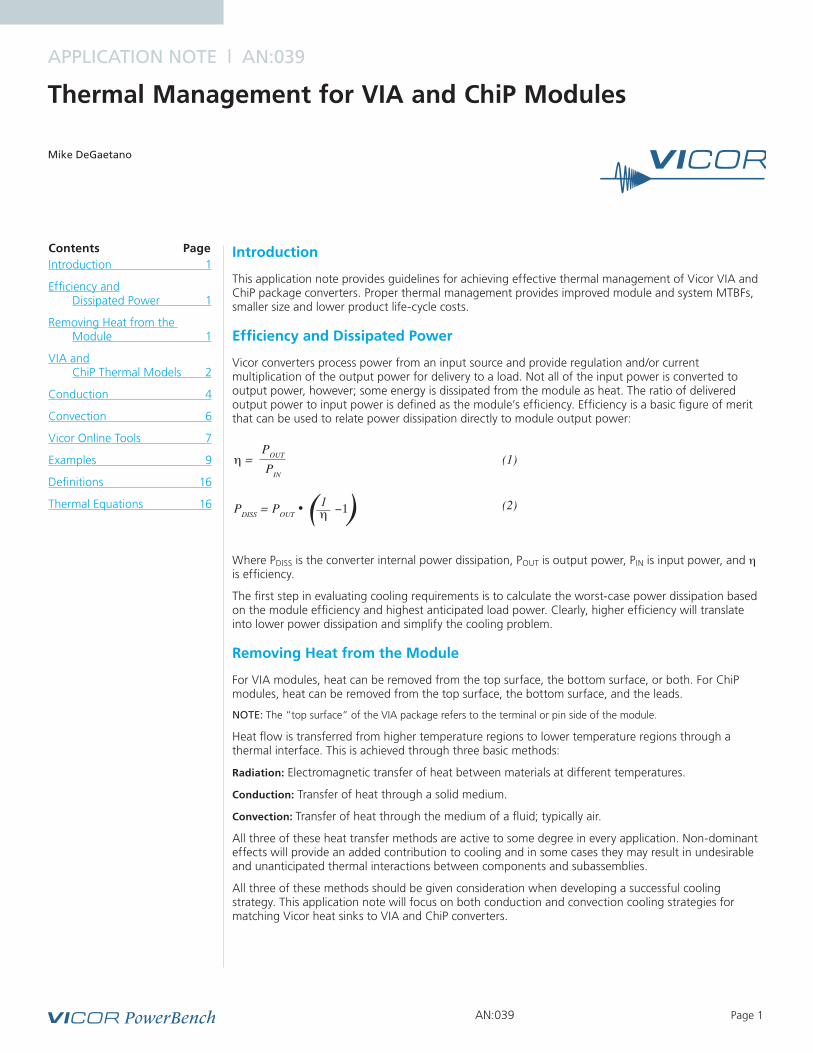
AN:039 Page 1
Introduction
This application note provides guidelines for achieving effective thermal management of Vicor VIA and ChiP package converters. Proper thermal management provides improved module and system MTBFs, smaller size and lower product life-cycle costs.
Efficiency and Dissipated Power
Vicor converters process power from an input source and provide regulation and/or current multiplication of the output power for delivery to a load. Not all of the input power is converted to output power, however; some energy is dissipated from the module as heat. The ratio of delivered output power to input power is defined as the module’s efficiency. Efficiency is a basic figure of merit that can be used to relate power dissipation directly to module output power:
Where PDISS is the converter internal power dissipation, POUT is output power, PIN is input power, and η is efficiency.
The first step in evaluating cooling requirements is to calculate the worst-case power dissipation based on the module efficiency and highest anticipated load power. Clearly, higher efficiency will translate into lower power dissipation and simplify the cooling problem.
Removing Heat from the Module
For VIA modules, heat can be removed from the top surface, the bottom surface, or both. For ChiP modules, heat can be removed from the top surface, the bottom surface, and the leads.
NOTE: The “top surface” of the VIA package refers to the terminal or pin side of the module.
Heat flow is transferred from higher temperature regions to lower temperature regions through a thermal interface. This is achieved through three basic methods:
Radiation: Electromagnetic transfer of heat between materials at different temperatures.
Conduction: Transfer of heat through a solid medium.
Convection: Transfer of heat through the medium of a fluid; typically air.
All three of these heat transfer methods are active to some degree in every application. Non-dominant effects will provide an added contribution to cooling and in some cases they may result in undesirable and unanticipated thermal interactions between components and subassemblies.
All three of these methods should be given consideration when developing a successful cooling strategy. This application note will focus on both conduction and convection cooling strategies for matching Vicor heat sinks to VIA and ChiP converters.
Thermal Management for VIA and ChiP Modules
APPLICATION NOTE | AN:039
Mike DeGaetano
Contents PageIntroduction 1
Efficiency and Dissipated Power 1
Removing Heat from the Module 1
VIA and ChiP Thermal Models 2
Conduction 4
Convection 6
Vicor Online Tools 7
Examples 9
Definitions 16
Thermal Equations 16
η =
( )1η
POUT
PIN
PDISS = POUT • −1
(1)
(2)
AN:039 Page 2
VIA and ChiP Thermal Models
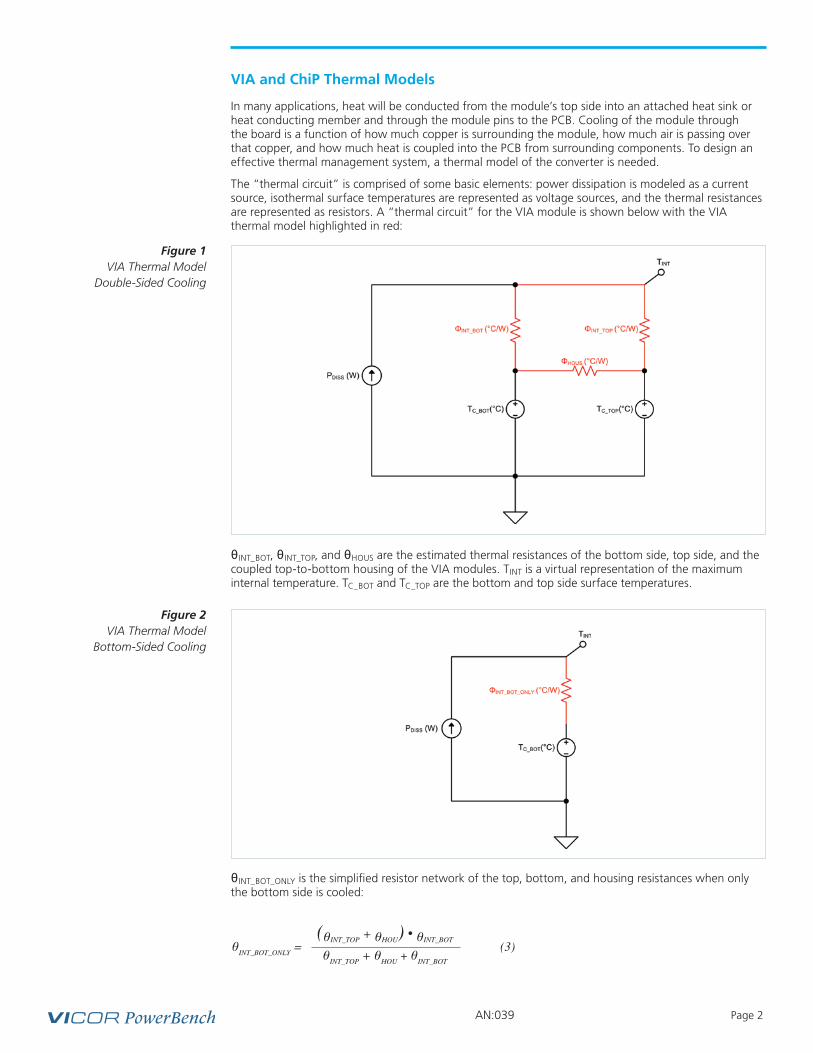
In many applications, heat will be conducted from the module’s top side into an attached heat sink or heat conducting member and through the module pins to the PCB. Cooling of the module through the board is a function of how much copper is surrounding the module, how much air is passing over that copper, and how much heat is coupled into the PCB from surrounding components. To design an effective thermal management system, a thermal model of the converter is needed.
The “thermal circuit” is comprised of some basic elements: power dissipation is modeled as a current source, isothermal surface temperatures are represented as voltage sources, and the thermal resistances are represented as resistors. A “thermal circuit” for the VIA module is shown below with the VIA thermal model highlighted in red:
θINT_BOT, θINT_TOP, and θHOUS are the estimated thermal resistances of the bottom side, top side, and the coupled top-to-bottom housing of the VIA modules. TINT is a virtual representation of the maximum internal temperature. TC_BOT and TC_TOP are the bottom and top side surface temperatures.
θINT_BOT_ONLY is the simplified resistor network of the top, bottom, and housing resistances when only the bottom side is cooled:
Figure 1 VIA Thermal Model
Double-Sided Cooling
Figure 2 VIA Thermal Model
Bottom-Sided Cooling
θINT_BOT_ONLY = (θINT_TOP + θHOU) • θINT_BOT
θINT_TOP + θHOU + θINT_BOT
(3)
AN:039 Page 3
θINT_TOP_ONLY is the simplified resistor network of the top, bottom, and housing resistances when only the top side is cooled:
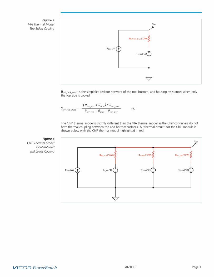
The ChiP thermal model is slightly different than the VIA thermal model as the ChiP converters do not have thermal coupling between top and bottom surfaces. A “thermal circuit” for the ChiP module is shown below with the ChiP thermal model highlighted in red:
Figure 3 VIA Thermal Model Top-Sided Cooling
θINT_TOP_ONLY = (θINT_BOT + θHOU) • θINT_TOP
θINT_TOP + θHOU + θINT_BOT
(4)
Figure 4 ChiP Thermal Model
Double-Sided and Leads Cooling
AN:039 Page 4
θINT_TOP, θINT_BOTTOM and θLEADS are the thermal resistance characteristics of the module; and the top and bottom surface temperatures are represented as TC_TOP and TC_BOT. TLEADS is the temperature of the PCB at the leads.
Conduction
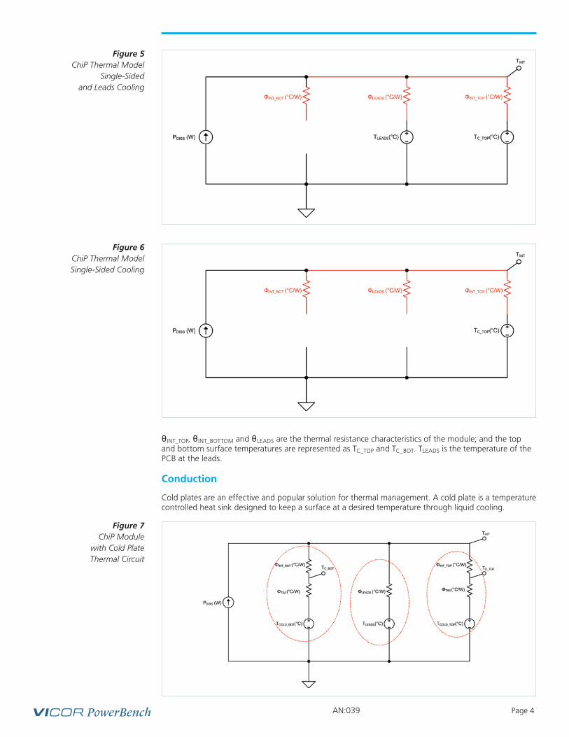
Cold plates are an effective and popular solution for thermal management. A cold plate is a temperature controlled heat sink designed to keep a surface at a desired temperature through liquid cooling.
Figure 5 ChiP Thermal Model
Single-Sided and Leads Cooling
Figure 6 ChiP Thermal Model Single-Sided Cooling
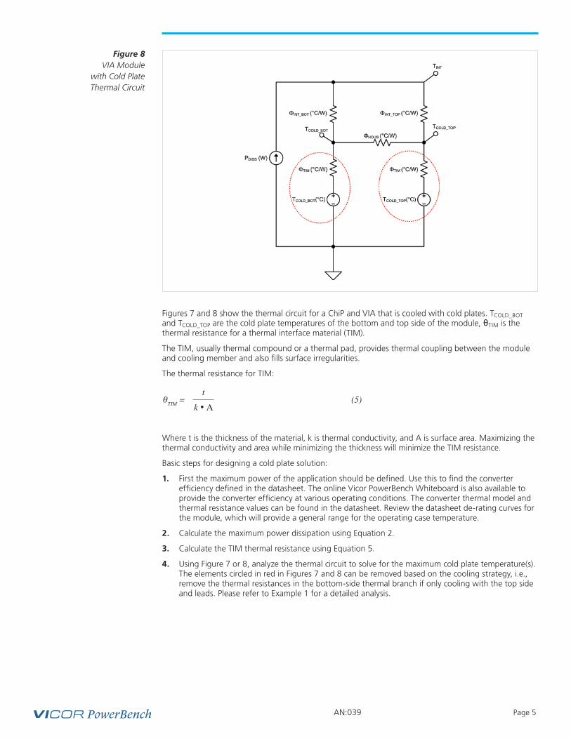
Figure 7 ChiP Module
with Cold Plate Thermal Circuit
AN:039 Page 5
Figure 8 VIA Module
with Cold Plate Thermal Circuit
Figures 7 and 8 show the thermal circuit for a ChiP and VIA that is cooled with cold plates. TCOLD_BOT and TCOLD_TOP are the cold plate temperatures of the bottom and top side of the module, θTIM is the thermal resistance for a thermal interface material (TIM).
The TIM, usually thermal compound or a thermal pad, provides thermal coupling between the module and cooling member and also fills surface irregularities.
The thermal resistance for TIM:
Where t is the thickness of the material, k is thermal conductivity, and A is surface area. Maximizing the thermal conductivity and area while minimizing the thickness will minimize the TIM resistance.
Basic steps for designing a cold plate solution:
1. First the maximum power of the application should be defined. Use this to find the converter efficiency defined in the datasheet. The online Vicor PowerBench Whiteboard is also available to provide the converter efficiency at various operating conditions. The converter thermal model and thermal resistance values can be found in the datasheet. Review the datasheet de-rating curves for the module, which will provide a general range for the operating case temperature.
2. Calculate the maximum power dissipation using Equation 2.
3. Calculate the TIM thermal resistance using Equation 5.
4. Using Figure 7 or 8, analyze the thermal circuit to solve for the maximum cold plate temperature(s). The elements circled in red in Figures 7 and 8 can be removed based on the cooling strategy, i.e., remove the thermal resistances in the bottom-side thermal branch if only cooling with the top side and leads. Please refer to Example 1 for a detailed analysis.
θTIM =t
k • Α(5)
AN:039 Page 6
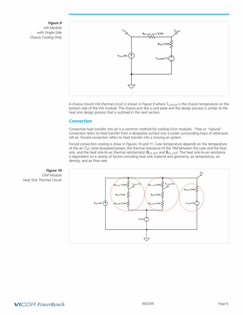
A chassis mount VIA thermal circuit is shown in Figure 9 where TCHASSIS is the chassis temperature on the bottom side of the VIA module. The chassis acts like a cold plate and the design process is similar to the heat sink design process that is outlined in the next section.
Convection
Convective heat transfer into air is a common method for cooling Vicor modules. “Free or “natural” convection refers to heat transfer from a dissipative surface into a cooler surrounding mass of otherwise still air. Forced convection refers to heat transfer into a moving air system.
Forced convection cooling is show in Figures 10 and 11. Case temperature depends on the temperature of the air (TA), total dissipated power, the thermal resistance of the TIM between the case and the heat sink, and the heat sink-to-air thermal resistance(s) (θHS_BOT and θHS_TOP). The heat sink-to-air resistance is dependent on a variety of factors including heat sink material and geometry, air temperature, air density, and air flow rate.
Figure 9 VIA Module
with Single-Side Chassis Cooling Only
Figure 10 ChiP Module
Heat Sink Thermal Circuit
AN:039 Page 7
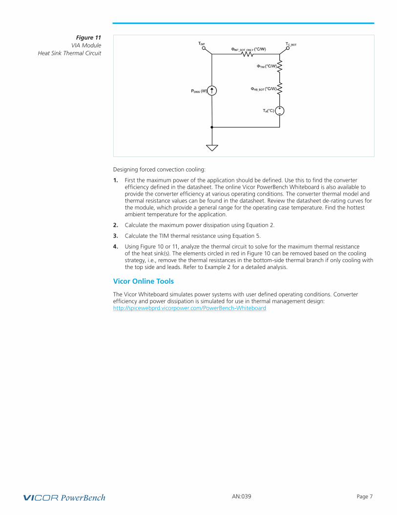
Figure 11 VIA Module
Heat Sink Thermal Circuit
Designing forced convection cooling:
1. First the maximum power of the application should be defined. Use this to find the converter efficiency defined in the datasheet. The online Vicor PowerBench Whiteboard is also available to provide the converter efficiency at various operating conditions. The converter thermal model and thermal resistance values can be found in the datasheet. Review the datasheet de-rating curves for the module, which provide a general range for the operating case temperature. Find the hottest ambient temperature for the application.
2. Calculate the maximum power dissipation using Equation 2.
3. Calculate the TIM thermal resistance using Equation 5.
4. Using Figure 10 or 11, analyze the thermal circuit to solve for the maximum thermal resistance of the heat sink(s). The elements circled in red in Figure 10 can be removed based on the cooling strategy, i.e., remove the thermal resistances in the bottom-side thermal branch if only cooling with the top side and leads. Refer to Example 2 for a detailed analysis.
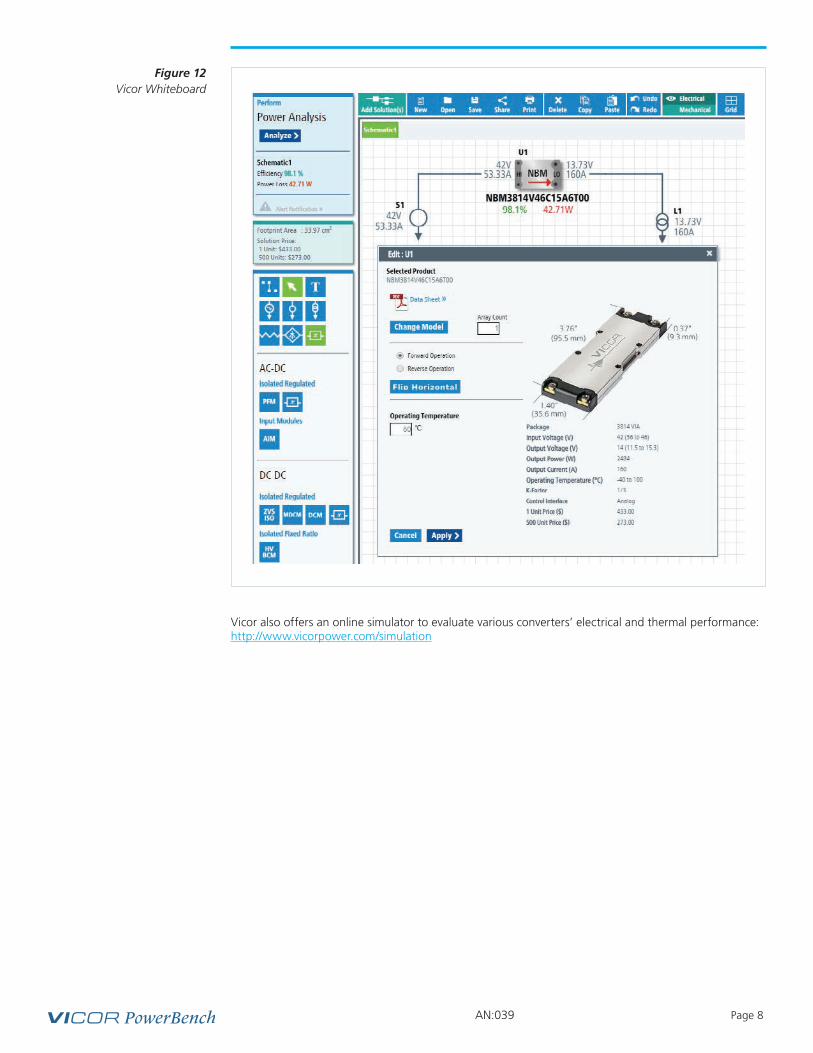
Vicor Online Tools
The Vicor Whiteboard simulates power systems with user defined operating conditions. Converter efficiency and power dissipation is simulated for use in thermal management design:http://spicewebprd.vicorpower.com/PowerBench-Whiteboard
AN:039 Page 8
Figure 12 Vicor Whiteboard
Vicor also offers an online simulator to evaluate various converters’ electrical and thermal performance: http://www.vicorpower.com/simulation
AN:039 Page 9
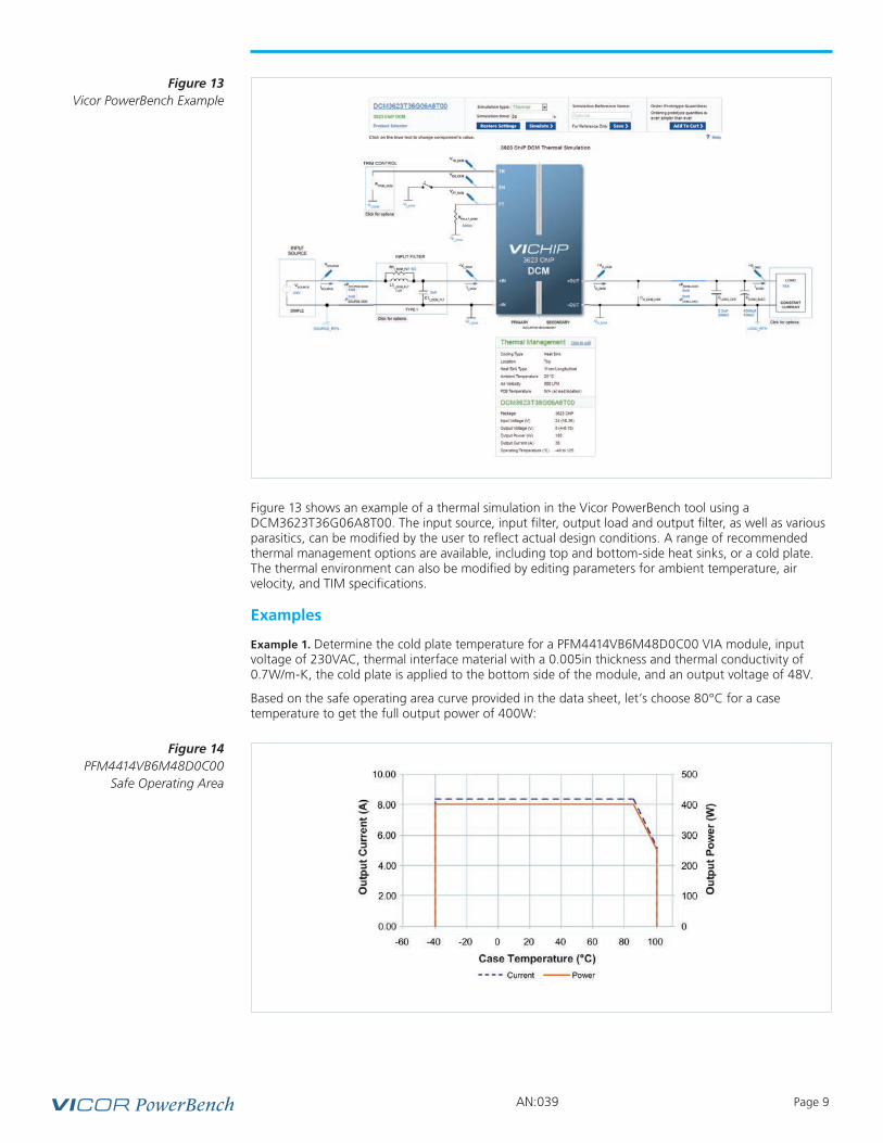
Figure 13 Vicor PowerBench Example
Figure 13 shows an example of a thermal simulation in the Vicor PowerBench tool using a DCM3623T36G06A8T00. The input source, input filter, output load and output filter, as well as various parasitics, can be modified by the user to reflect actual design conditions. A range of recommended thermal management options are available, including top and bottom-side heat sinks, or a cold plate. The thermal environment can also be modified by editing parameters for ambient temperature, air velocity, and TIM specifications.
Examples
Example 1. Determine the cold plate temperature for a PFM4414VB6M48D0C00 VIA module, input voltage of 230VAC, thermal interface material with a 0.005in thickness and thermal conductivity of 0.7W/m-K, the cold plate is applied to the bottom side of the module, and an output voltage of 48V.
Based on the safe operating area curve provided in the data sheet, let’s choose 80°C for a case temperature to get the full output power of 400W:
Figure 14 PFM4414VB6M48D0C00
Safe Operating Area
AN:039 Page 10
What we know so far:
From the datasheet:
The single-sided cooling thermal resistance for the VIA can be calculated:
The bottom-side surface area of the 4414 VIA is 111mm x 36mm. The TIM thermal resistance can be found:
The power dissipation can be calculated:
TC_BOT = 80°CPOUT = 400W
k = 0.7
t = 0.005in = 127 • 10-6mn = 92% (full load, 230VAC, 80°C case temp)
WmK
θINT_TOP = 1.34
θINT_BOT = 1.72
θHOUS = 0.57
°CW°CW
°CW
θINT_BOT_ONLY = (θINT_TOP + θHOU) • θINT_BOT
θINT_TOP + θHOU + θINT_BOT
θINT_BOT_ONLY = = 0.905
°CW
°CW
°CW (1.34 + 0.57 ) • 1.72
°CW
°CW
°CW 1.34 + 0.57 + 1.72
°CW
θTIM =t
k • Α=
127 • 10-6m
0.7 •.111m • .036mW
mK
= 0.045°CW
PDISS = 400W • −1 = 34.78W
( )1η
PDISS = POUT • −1
( )10.92
AN:039 Page 11
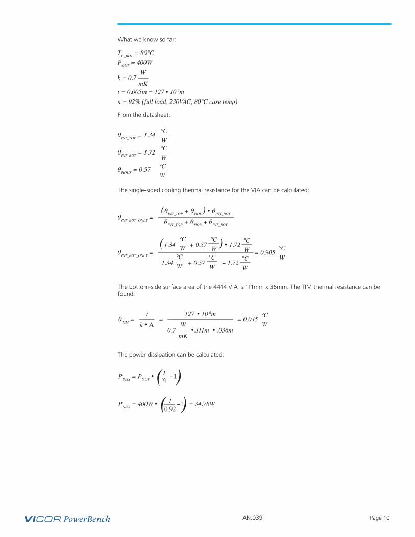
Figure 15 Thermal Circuit
Using the thermal circuit, we can now write the equation to calculate the maximum cold plate temperature:
In this case, the cold plate temperature nearly matches the case temperature as the thermal resistance of the TIM is very small. The thermal resistance of the VIA was not needed in this example as the case temperature chosen from the safe operating area curve provided the thermal boundary to ensure full power operation.
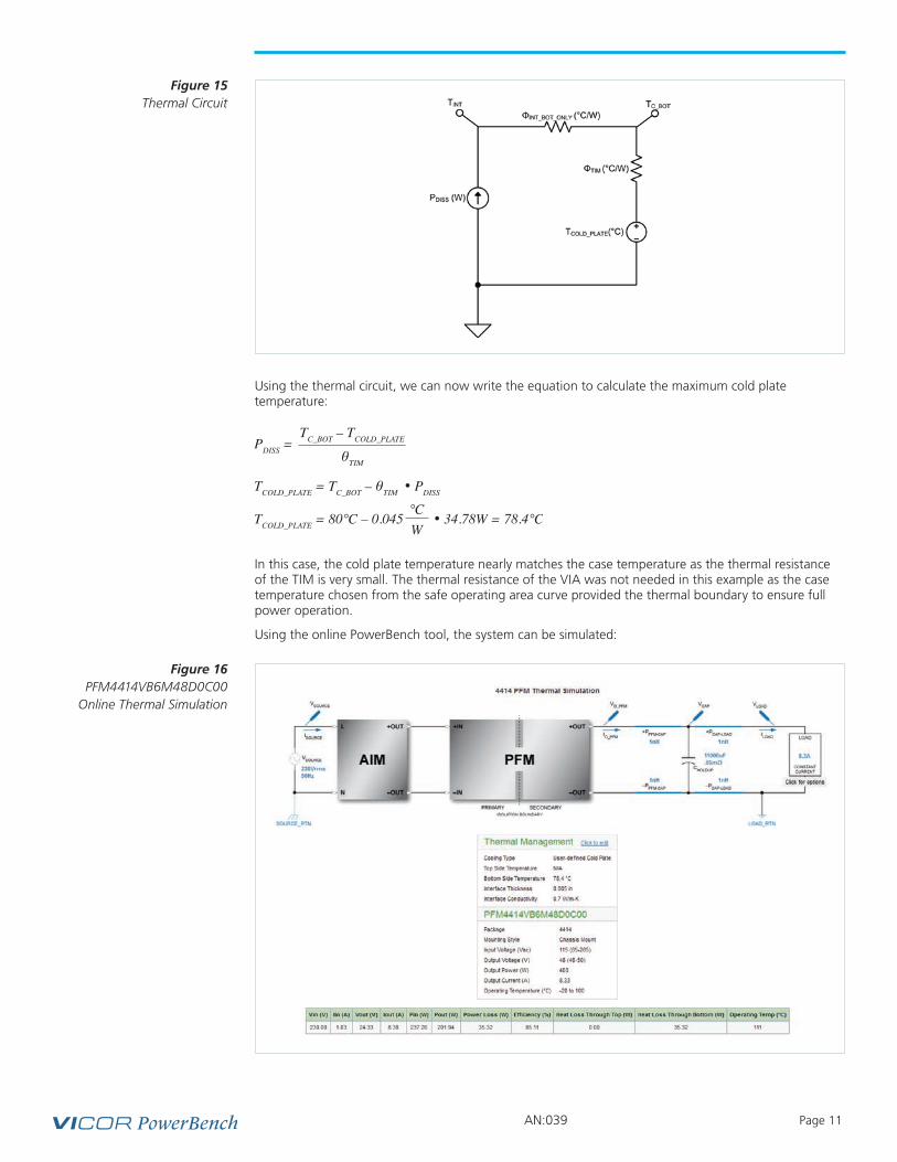
Using the online PowerBench tool, the system can be simulated:
PDISS =
TCOLD_PLATE = TC_BOT – θTIM • PDISS
TCOLD_PLATE = 80°C – 0.045 • 34.78W = 78.4°C
TC_BOT – TCOLD_PLATE
θTIM
°CW
Figure 16 PFM4414VB6M48D0C00
Online Thermal Simulation
AN:039 Page 12
Although the part can process full power with a case temperature of 80°C, it is desirable to maintain an internal temperature as low as possible to increase reliability and operating life. Reducing power dissipation, external thermal resistance(s), cold plate temperature, or ambient air temperature will minimize the converter’s internal operating temperature. A general rule-of-thumb for operating temperature states that a 10°C decrease in operating temperature doubles reliability and operating life of the internal components.
Another strategy to reduce the internal operating temperature is to use two or more parallel converters in place of a single converter. The thermal resistance for each converter remains the same, but the resultant heat flow for each is effectively divided. The total dissipated power is divided among the converters, therefore the internal operating temperature rise is also divided.
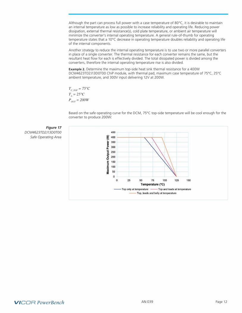
Example 2. Determine the maximum top-side heat sink thermal resistance for a 400W DCM4623TD2J13D0T00 ChiP module, with thermal pad, maximum case temperature of 75°C, 25°C ambient temperature, and 300V input delivering 12V at 200W.
Based on the safe operating curve for the DCM, 75°C top-side temperature will be cool enough for the converter to produce 200W:
TC_TOP = 75°CTA = 25°CPOUT = 200W
Figure 17 DCM4623TD2J13D0T00
Safe Operating Area
AN:039 Page 13
Figure 18 DCM4623TD2J13D0T00
Whiteboard
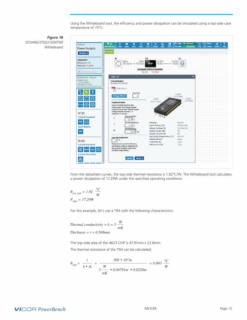
Using the Whiteboard tool, the efficiency and power dissipation can be simulated using a top-side case temperature of 75°C:
From the datasheet curves, the top-side thermal resistance is 1.92°C/W. The Whiteboard tool calculates a power dissipation of 17.29W under the specified operating conditions.
For this example, let’s use a TIM with the following characteristics:
The top-side area of the 4623 ChiP is 47.91mm x 22.8mm.
The thermal resistance of the TIM can be calculated:
θINT_TOP = 1.92
PDISS = 17.29W
°CW
Thermal conductivity = k = 5
Thickness = t = 0.508mm
WmK
θTIM =t
k • Α=
508 • 10-6m
5 • 0.04791m • 0.0228mW
mK
= 0.093 °CW
AN:039 Page 14
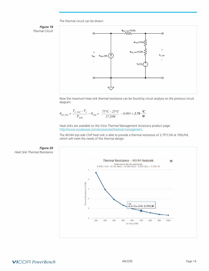
The thermal circuit can be drawn:
Now the maximum heat sink thermal resistance can be found by circuit analysis on the previous circuit diagram:
Heat sinks are available on the Vicor Thermal Management Accessory product page: http://www.vicorpower.com/accessories/thermal-management
The 40144 top-side ChiP heat sink is able to provide a thermal resistance of 2.75°C/W at 700LFM, which will meet the needs of this thermal design:
Figure 19 Thermal Circuit
θHS_TOP = – θTIM = – 0.093 = 2.78 TC_TOP – TA
PDISS
75°C – 25°C17.29W
°CW
Figure 20 Heat Sink Thermal Resistance
AN:039 Page 15
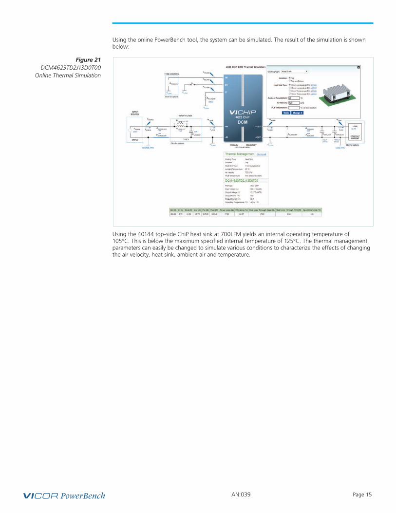
Using the online PowerBench tool, the system can be simulated. The result of the simulation is shown below:
Using the 40144 top-side ChiP heat sink at 700LFM yields an internal operating temperature of 105°C. This is below the maximum specified internal temperature of 125°C. The thermal management parameters can easily be changed to simulate various conditions to characterize the effects of changing the air velocity, heat sink, ambient air and temperature.
Figure 21 DCM4623TD2J13D0T00
Online Thermal Simulation
AN:039 Page 16
Definitions
A = TIM surface area
k = TIM thermal conductivity
η = efficiency = POUT/PIN
θHS_BOT = bottom-side heat sink thermal resistance
θHS_TOP = top-side heat sink thermal resistance
θHOU = thermal coupling resistance between top and bottom case for VIA package
θINT_BOT = bottom case thermal resistance
θINT_BOT_ONLY = equivalent thermal resistance for VIA bottom side cooling thermal model
θINT_TOP = top case thermal resistance
θINT_TOP_ONLY = equivalent thermal resistance for VIA top side cooling thermal model
θLEADS = thermal resistance of leads for ChiP module
θTIM = thermal interface material thermal resistance
t = TIM thickness
TA = ambient air temperature
TC_BOT = bottom case temperature
TCHASSIS = chassis temperature
TC_TOP = top case temperature
TINT = internal module temperature
TLEADS = leads temperature for ChiP module
TMAX = maximum case temperature (available in datasheet)
Thermal Equations
η =
( )1η
POUT
PIN
PDISS = POUT • −1
Efficiency =
Dissipated power =
Thermal interface material thermal resistance = θTIM =t
k • Α
Limitation of WarrantiesInformation in this document is believed to be accurate and reliable. HOWEVER, THIS INFORMATION IS PROVIDED “AS IS” AND WITHOUT ANY WARRANTIES, EXPRESSED OR IMPLIED, AS TO THE ACCURACY OR COMPLETENESS OF SUCH INFORMATION. VICOR SHALL HAVE NO LIABILITY FOR THE CONSEQUENCES OF USE OF SUCH INFORMATION. IN NO EVENT SHALL VICOR BE LIABLE FOR ANY INDIRECT, INCIDENTAL, PUNITIVE, SPECIAL OR CONSEQUENTIAL DAMAGES (INCLUDING, WITHOUT LIMITATION, LOST PROFITS OR SAVINGS, BUSINESS INTERRUPTION, COSTS RELATED TO THE REMOVAL OR REPLACEMENT OF ANY PRODUCTS OR REWORK CHARGES).
Vicor reserves the right to make changes to information published in this document, at any time and without notice. You should verify that this document and information is current. This document supersedes and replaces all prior versions of this publication.
All guidance and content herein are for illustrative purposes only. Vicor makes no representation or warranty that the products and/or services described herein will be suitable for the specified use without further testing or modification. You are responsible for the design and operation of your applications and products using Vicor products, and Vicor accepts no liability for any assistance with applications or customer product design. It is your sole responsibility to determine whether the Vicor product is suitable and fit for your applications and products, and to implement adequate design, testing and operating safeguards for your planned application(s) and use(s).
VICOR PRODUCTS ARE NOT DESIGNED, AUTHORIZED OR WARRANTED FOR USE IN LIFE SUPPORT, LIFE-CRITICAL OR SAFETY-CRITICAL SYSTEMS OR EQUIPMENT. VICOR PRODUCTS ARE NOT CERTIFIED TO MEET ISO 13485 FOR USE IN MEDICAL EQUIPMENT NOR ISO/TS16949 FOR USE IN AUTOMOTIVE APPLICATIONS OR OTHER SIMILAR MEDICAL AND AUTOMOTIVE STANDARDS. VICOR DISCLAIMS ANY AND ALL LIABILITY FOR INCLUSION AND/OR USE OF VICOR PRODUCTS IN SUCH EQUIPMENT OR APPLICATIONS AND THEREFORE SUCH INCLUSION AND/OR USE IS AT YOUR OWN RISK.
Terms of SaleThe purchase and sale of Vicor products is subject to the Vicor Corporation Terms and Conditions of Sale which are available at: (http://www.vicorpower.com/termsconditionswarranty)
Export ControlThis document as well as the item(s) described herein may be subject to export control regulations. Export may require a prior authorization from U.S. export authorities.
02/17
Contact Us: http://www.vicorpower.com/contact-us
Vicor Corporation25 Frontage Road
Andover, MA, USA 01810Tel: 800-735-6200Fax: 978-475-6715
www.vicorpower.com
emailCustomer Service: [email protected]
Technical Support: [email protected]
©2017 Vicor Corporation. All rights reserved. The Vicor name is a registered trademark of Vicor Corporation.All other trademarks, product names, logos and brands are property of their respective owners.
Rev 1.0 Page 17