Embed Size (px)
Citation preview
3D-IC Dynamic Thermal Analysis with
Hierarchical and Configurable Chip Thermal
Model
Stephen H. Pan and Norman Chang
Apache Design, Inc.
Subsidiary of ANSYS, Inc.
San Jose, CA, USA
Tadaaki Hitomi
Apache Design, Inc.
Subsidiary of ANSYS, Inc.
Tokyo, Japan
Abstract— The thermal response in 3D-IC is important for its
impact on chip sign-off for thermal sensor placement, Tmax
control, and thermal-aware electro-migration (EM). Thermal
responses in 3D-IC, for either steady state or transient, are
strongly coupled with surrounding components, i.e., package,
board, and system. This study verified that in a chip-package-
system (CPS) 3D-IC environment, the time it took to reach a
steady state in chip thermal dynamics can take more than tens of
seconds or longer, instead of the mili, micro, or nano seconds
seen in many articles using a chip-only thermal model. High
frequency power oscillations will not lead to significant
temperature variations in chips, due to the high thermal
capacitance in the surrounding environment. The most practical
power modes for dynamic thermal analysis are the average ones
in chip activities, e.g., Chip Thermal Model (CTM), based on
either vectorless or event-driven activities in a chip. CTMs for
3D-IC can be implemented in a hierarchical or configurable way.
With power activities on and off in sequence, transient responses
in 3D-IC can be simulated efficiently using Green’s functions of
power-on transients. Sample cases of thermal analysis based on
power modes from different operating activities, and high-low
power switching are presented here.
Keywords—3D-IC; CTM; power activity modes; Green’s
function; heat capacity; thermal transients; CPS
I. INTRODUCTION
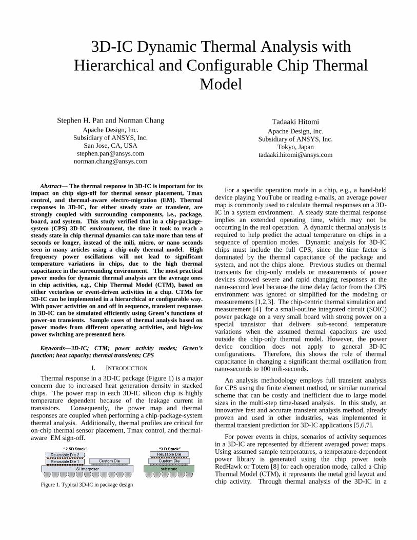
Thermal response in a 3D-IC package (Figure 1) is a major concern due to increased heat generation density in stacked chips. The power map in each 3D-IC silicon chip is highly temperature dependent because of the leakage current in transistors. Consequently, the power map and thermal responses are coupled when performing a chip-package-system thermal analysis. Additionally, thermal profiles are critical for on-chip thermal sensor placement, Tmax control, and thermal-aware EM sign-off.
Figure 1. Typical 3D-IC in package design
For a specific operation mode in a chip, e.g., a hand-held device playing YouTube or reading e-mails, an average power map is commonly used to calculate thermal responses on a 3D-IC in a system environment. A steady state thermal response implies an extended operating time, which may not be occurring in the real operation. A dynamic thermal analysis is required to help predict the actual temperature on chips in a sequence of operation modes. Dynamic analysis for 3D-IC chips must include the full CPS, since the time factor is dominated by the thermal capacitance of the package and system, and not the chips alone. Previous studies on thermal transients for chip-only models or measurements of power devices showed severe and rapid changing responses at the nano-second level because the time delay factor from the CPS environment was ignored or simplified for the modeling or measurements [1,2,3]. The chip-centric thermal simulation and measurement [4] for a small-outline integrated circuit (SOIC) power package on a very small board with strong power on a special transistor that delivers sub-second temperature variations when the assumed thermal capacitors are used outside the chip-only thermal model. However, the power device condition does not apply to general 3D-IC configurations. Therefore, this shows the role of thermal capacitance in changing a significant thermal oscillation from nano-seconds to 100 mili-seconds.
An analysis methodology employs full transient analysis for CPS using the finite element method, or similar numerical scheme that can be costly and inefficient due to large model sizes in the multi-step time-based analysis. In this study, an innovative fast and accurate transient analysis method, already proven and used in other industries, was implemented in thermal transient prediction for 3D-IC applications [5,6,7].
For power events in chips, scenarios of activity sequences in a 3D-IC are represented by different averaged power maps. Using assumed sample temperatures, a temperature-dependent power library is generated using the chip power tools RedHawk or Totem [8] for each operation mode, called a Chip Thermal Model (CTM), it represents the metal grid layout and chip activity. Through thermal analysis of the 3D-IC in a
system environment, the step function transient response or Green’s function map, due to turning-on the CTM power map on each chip, is calculated and stored. In 3D-IC, multiple CTMs are applied at the same time in one activity mode of the device. This is repeated for different 3D-IC power activities to obtain step function responses for all chips in the CPS environment. The dynamic response of any location on the 3D-IC caused by a sequence of activities can be calculated using a convolution integral or Green’s function approach [5,6,7]. This is based on the step function thermal responses, with the assumptions of the thermal process being quasi-static and the principle of linear superposition holds. This calculation is very efficient compared to a full transient analysis of the entire thermal system, and is also accurate.
A CTM generation for a full-chip may not be possible for a 3D-IC designer, since only details of a few blocks are available in theearly design phase. A hierarchical block-level CTM can be generated with partial details in a system-on-chip (SoC) for different activity modes. The chip and 3D-IC architect can then configure different activity-driven CTMs for a realistic 3D-IC transient thermal analysis. For intellectual property (IP) blocks in a chip having power estimates without CTM representation, they can be included as simple power blocks together with block CTMs in a SoC, and CTMs or uniform power on other chips in the complete 3D-IC thermal analysis. This is a hierarchical and configurable CTM-based approach used in an ANSYS and Sentinel-TI tool flow for 3D-IC thermal [9,10].
In the following sections, the thermal transient for 3D-IC will be described first, emphasizing the importance of the complete CPS environment. The effects of thermal capacitance in CPS to chip thermal transients are demonstrated by a CPS versus chip-only transient model. Next, the Green’s function approach for chip thermal transient will be introduced for its efficiency and flexibility. The role of CTMs in the multi-activity transient analysis for 3D-IC will also be described. To finish, two CPS designs and power transient scenarios will be presented for hierarchical and configurable use of CTMs.
II. THERMAL TRANSIENT IN 3D IC
A. Law of Heat Transfer and Thermal Boundary Conditions
The governing equation in heat transfer phenomenon for 3D-
IC chips in package, on board, or in system is:
)1(t
Tc
z
TK
zy
TK
yx
TK
xzyx
T = T(x,y,z;t) = Temperature Distribution
Kx = Thermal Conductivity in the x-direction, W/m-C
Ky = Thermal Conductivity in the y-direction
Kz = Thermal Conductivity in the z-direction
r = Mass Density, Kg/m3
c = Specific heat of material, J/Kg-C
For constant thermal conductivity (K), the equation is written
as:
t
Tc
z
T
y
T
x
TK
2
2
2
2
2
2
or:
)2(12
2
2
2
2
2
t
T
z
T
y
T
x
T
rc = Heat capacity per unit volume
a=K/rc = Thermal diffusivity
The purpose of performing thermal analysis for 3D-IC is to
provide accurate temperature responses in chips. The thermal
sensor placement, Tmax control, and chip EM sign-offs
depend on an accurate thermal profile on-chip. While a steady
state thermal profile is important in the process, knowledge of
transients at hot spots is also desirable.
A commonly used solution process is using finite element
(FE) modeling of the complex 3D-IC structure (Figure 1), and
the step-by-step numerical schemes in transient calculations.
Power maps for 3D-IC design are applied on the surface of
chips, e.g., using equivalent heat transfer coefficients (HTC).
The boundary conditions on exposed surfaces of the structure
can be either from empirical-based heat transfer coefficients or
from computational fluid dynamics (CFD) simulation [11] of
system air flow. In the transient simulation process, power
maps are assigned as time-varying loadings, using time-
stepping at appropriate increments. Results for each time-step
are saved so that the thermal transient responses in 3D-IC can
be reviewed.
With the progress of chip technology nodes, e.g., 28-
nanometer (nm) and beyond, most complications are from the
high temperature dependency of power, due to leakage in chip
device layers and self-heating on wires in the interconnection.
The distribution of power must be consistent to the thermal
profile in 3D-IC which generates another level of complexity
in transient analysis. Iterations for converged temperature and
power are needed [10]. The granularity of temperature and
power maps is also important for accuracy, i.e., more details in
chip modeling alone. When coupling of the power calculation
is included in the power-thermal loop, the detailed thermal
analysis on the chips in 3D-IC is a challenge.
However, with Green’s the function approach and linear
superposition assumption, thermal transient responses in 3D-
IC become practical. Next we will review the nature of power
transients in a chip and its effects in thermal responses. Then,
a practical transient approach is proposed to manage the needs
of accurate thermal analysis for each chip, i.e., granularity
thermal and power map in each chip, and efficient transient
calculation of hot spots in 3D-IC.
B. Thermal Transient of Chip in Package/System
For a chip-only thermal model, temperature response in a
CMOS-based chip can be quick when the power is on, e.g.,
reaching steady state in about 0.06 sec. in a 11.3x14.4mm chip
[1]. For such a small time scale, it seems that rapid power
variations in mili seconds or smaller should be accounted for
in the thermal transient calculation. However, this quick
thermal response in the chip is not likely to happen in a real
application of either the conventional or 3D-IC in a normal
package on board, or in a system due to the coupling of
thermal capacitance from thermally affected components, e.g.,
package and part of the board [12]. These are demonstrated in
a test case below.
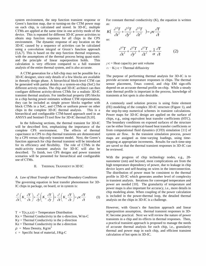
A chip/package on board analysis model (Figure 2), is used to
review the effects of heat capacities to the temperature rise. A
2.9x3mm chip in a 5x5mm BGA package is mounted on a
100x100mm 4L board, with heat capacity assigned to all the
materials. A power up transient analysis [9,10] shows that the
time to reach a steady state on the chip is more than 100
seconds (Figure 3). But, if the heat capacity in the materials
outside the die is set to zero, the time to reach a steady state
dropped to around 0.6 seconds, i.e., chip temperature will
respond quickly to power changes in a few hundred mili-
seconds (Figure 4).
Reviewing the volumetric capacitance distribution in this CPS
helpsto explain the temperature rise time differences. Due to
the exponential temperature decay off the edges of the
package, not all the thermal capacitance on the large board
affects the chip’s thermal transients [12]. In this case, a small
piece of board measuring 13.9x14.5mm under the package
from the 100x100mm board, is used in the volumetric thermal
capacitance calculation based on calculated temperature decay
on the board. From this total volumetric capacitance, only
0.05% is from the chip, 5.21% is from the package, and
94.79% is from the small board piece. The time factor in
power-up transients is dominated by thermal capacitance
outside the die. Hence, caution must be taken when
analyzing thermal transient on chip that proper heat capacity
in the package and board are accounted for.
Figure 2. Thermal model of a 3x3mm chip in package of 5x5mm on thermal
board of 100x100mm with thermal contours from Sentinel-TI [10].
Figure 3. Temperature rise in a chip. Ignoring heat capacitance in package and
board will make the temperature rise unrealistically fast.
Figure 4. Zoom in view of the chip-only thermal response, reaching steady
state around 0.6 seconds
C. Full Thermal Transient and Green’s Function Approach
The FE model for a 3D-IC package in system can be large,
especially when small features in power maps are included in
chips and reflected in the fine FE meshes. It would be costly
to perform the solution steps thousands of times in the full
thermal transient analysis. Since the thermal conduction
process is quasi-static and linear-superposition applies [5,6,7],
the temperature transient response for any location in the FE
model can be calculated through a convolution integral, using
Green’s function of temperature from the step change of
power on chips [4,5]. The convolution integral is:
)3()(
,,,,,,0
d
PtzyxTtzyxT
t
S
Here, T is the temperature as a function of space location and
time, t and t. P represents the power on chips, which has
spatial distribution or a map that varies with the time
parameter t. TS is the step function response of T, due to a
power-on scenario.

Given P, with the knowledge of TS, temperature T at any
location (x, y, z) at any time instances (t), can be calculated in
a straight forward way. TS at any location can be calculated
from the time to a steady state solution, shown in Figure 3.
Figure 5 shows the comparison of thermal results using full
transient and Green’s function for a 40-sec. power-on and off
scenario in a CPS environment. The small differences in the
curves are because the TS used in Green’s function approach
was from a reduced two-stage model extracted from the full
FE model [10,12], in Figure 2. If TS is also calculated from a
full FE transient analysis, using either ANSYS/Mechanical[9]
or ANSYS Icepak[11], the two curves in Figure 5 will match
exactly. For the speed in a transient solution, the Green’s
function approach is at least 60x faster in this problem of only
14384 degrees of freedom in the FE model. For larger FE
models, the differences in simulation time will be more
significant since the Green’s function approach is independent
of FE model size after the TS is generated.
Figure 5. Comparison of temperature response on a hot spot on chip using full
thermal transient and Green’s function approach
D. Power Modes
The power calculation from the chip power tool [8] is
commonly refers to average cycle power consumption of all
cell instances in a chip. If the full-chip Value Change Dump
(VCD) file is available, the average power is based on event-
driven calculation. If no VCD file is available, the average
power is based on a vectorless calculation using an estimated
toggle rate. There could also be a mixed-mode, when only
some parts of the design have VCD data. The dynamic
performance of the chip is included in the average cycle power
calculation, and the power can be treated as static.
Chip power is related to the usage mode. For a smart phone
application, the power map and consumption level can be
different for voice communication, watching movie, or
reading e-mails. Another example of power control in a chip
is when the temperature sensor in the chip finds the limit
being exceeded in the high-performance power mode, so it
will switch to a low-power mode at a lower performance until
the temperature at the sensor location drops to a certain level.
For thermal transient prediction, different power maps should
be generated and applied to 3D-IC CPS as a series of thermal
source stimulus.
Using Green’s function approach for each power mode, a
template TS at a hot spot is represented by a temperature rising
timetable, similar to that in Figure 3, and will be generated
and saved. Since chips occupy only a small volume in the
CPS system, TS at any location for chips in a package behave
similarly, i.e., reaching a steady state at the same time in a
similar wave form. Hence, TS at any location in the chips can
be proportionately derived from the template accurately,
regardless of the chip power level and distribution. The
T(x,y,z,t) in equation (3) is readily available after TS(x,y,z,t) is
calculated, based on the template. For a different time series
of power modes represented by ∂P/∂t in equation (3), e.g., a
combination of high power and low power modes, the
temperature response at any location such as the one in Figure
5 is calculated.
E. Chip Thermal Model
In modern designs, chip power has strong temperature
dependency primarily due to leakage in the transistors, so
iterations for chip temperature and power maps are necessary
for an accurate power map [13,14] to get the TS for transient
calculation. The temperature-dependent power library called a
Chip Thermal Model (CTM), is generated from the chip
power tool [8]. Using CTM, a chip thermal tool [10] is
sufficient to generate converged thermal and power results,
i.e., no need to couple with a chip power tool for the solution.
CTMs for a 3D-IC package can be hierarchical, i.e., a power
map library assigned to multiple sub-regions in a chip, e.g.,
blocks/clusters in a SoC. It can also be adapted to chips in
configurable stacks in 3D-IC. In the next section, two test
cases will be presented using the CTM and Green’s function
approach to predict thermal transients at locations in a wire-
bond BGA and in a 3D-IC design with flip chips.
III. TEST CASES AND RESULTS
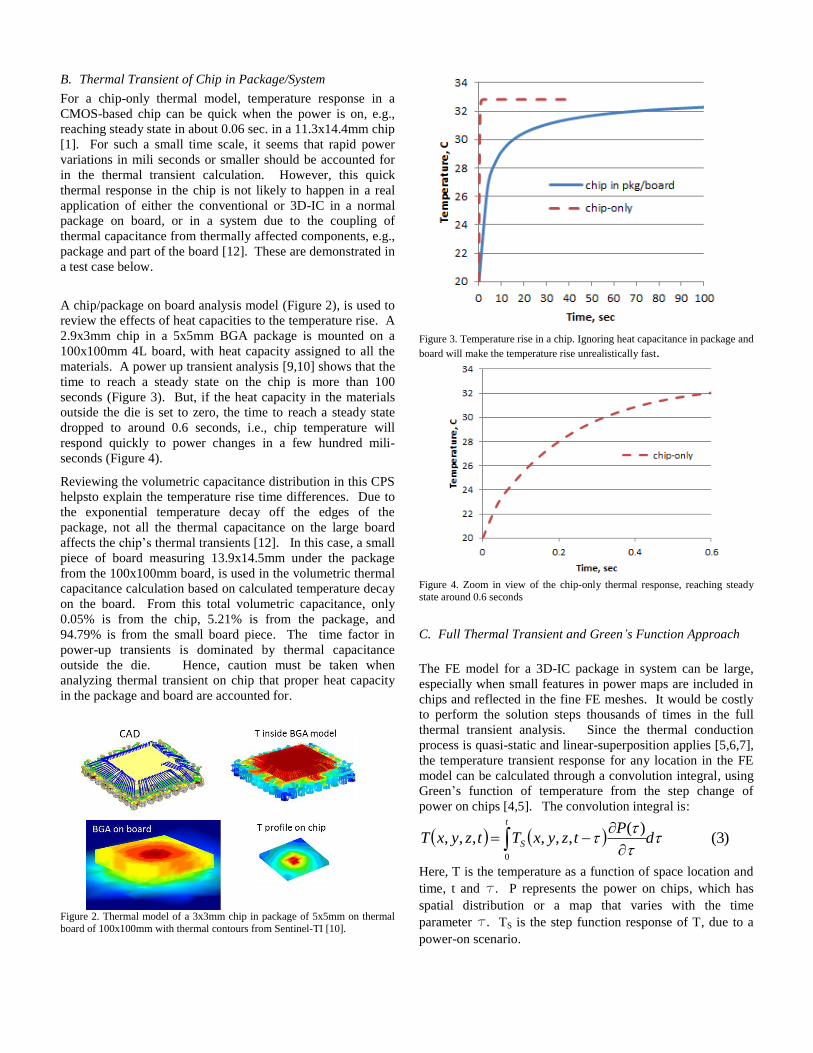
A. Trainsients in BGA from a Series of Power Activities
The BGA package is shown in Figure 6, with substrate sizes
of 16x16mm, 240 solder joints, and a wire-bond die of
5x5.1mm. The Theta_JA ranges from 76 to 81 C/W,
depending on how localized the power is allocated in the chip.
This BGA is mounted on a 100x100mm 4L thermal board in a
horizontal position. The ambient temperature was set at 20C
in still air. The chip power is generated in the chip power
tools [8] as shown in Figure 7, with three different power
modes or activities, i.e., a CTM for each of the conditions #1
to #3, with different power switching conditions. Figure 8
shows an example of the power map and temperature profiles
on-chip and in package for condition #1. Transients were
calculated at several locations, as shown in Figure 9. Figure
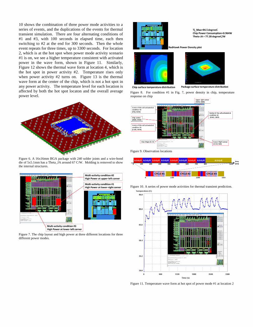
10 shows the combination of three power mode activities to a
series of events, and the duplications of the events for thermal
transient simulation. There are four alternating conditions of
#1 and #3, with 100 seconds in elapsed time, each then
switching to #2 at the end for 300 seconds. Then the whole
event repeats for three times, up to 3300 seconds. For location
2, which is at the hot spot when power mode activity scenario
#1 is on, we see a higher temperature consistent with activated
power in the wave form, shown in Figure 11. Similarly,
Figure 12 shows the thermal wave form at location 4, which is
the hot spot in power activity #2. Temperature rises only
when power activity #2 turns on. Figure 13 is the thermal
wave form at the center of the chip, which is not a hot spot in
any power activity. The temperature level for each location is
affected by both the hot spot locaton and the overall average
power level.
Figure 6. A 16x16mm BGA package with 240 solder joints and a wire-bond
die of 5x5.1mm has a Theta_JA around 67 C/W. Molding is removed to show the internal structures.
Figure 7. The chip layout and high power at three different locations for three
different power modes.
Figure 8. For condition #1 in Fig. 7, power density in chip, temperature
response on chip
Figure 9. Observation locations
Figure 10. A series of power mode activities for thermal transient prediction.
Figure 11. Temperature wave form at hot spot of power mode #1 at location 2
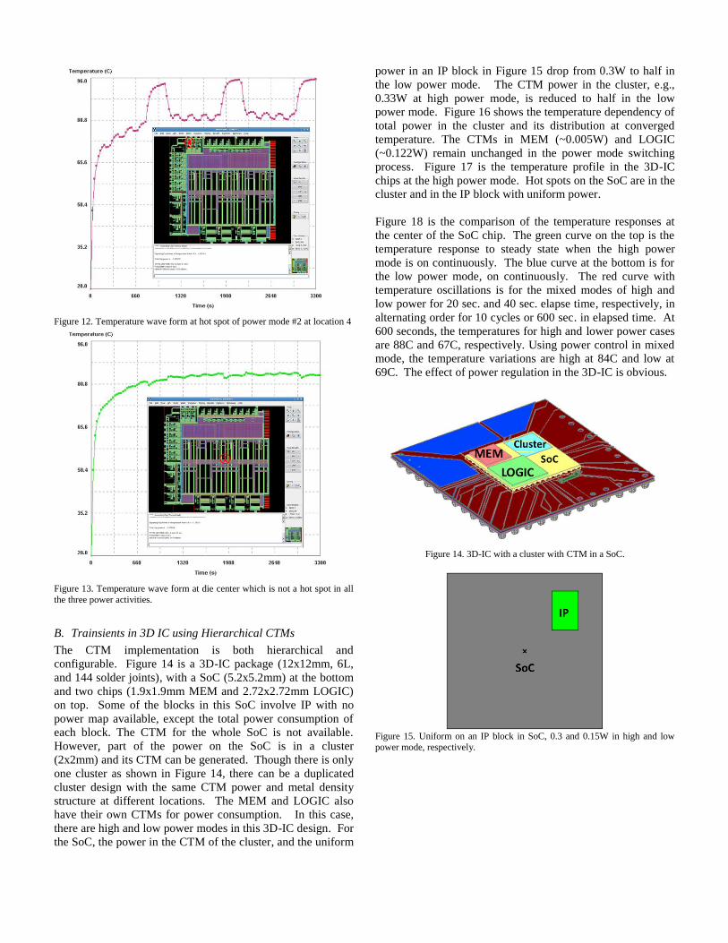
Figure 12. Temperature wave form at hot spot of power mode #2 at location 4
Figure 13. Temperature wave form at die center which is not a hot spot in all
the three power activities.
B. Trainsients in 3D IC using Hierarchical CTMs
The CTM implementation is both hierarchical and
configurable. Figure 14 is a 3D-IC package (12x12mm, 6L,
and 144 solder joints), with a SoC (5.2x5.2mm) at the bottom
and two chips (1.9x1.9mm MEM and 2.72x2.72mm LOGIC)
on top. Some of the blocks in this SoC involve IP with no
power map available, except the total power consumption of
each block. The CTM for the whole SoC is not available.
However, part of the power on the SoC is in a cluster
(2x2mm) and its CTM can be generated. Though there is only
one cluster as shown in Figure 14, there can be a duplicated
cluster design with the same CTM power and metal density
structure at different locations. The MEM and LOGIC also
have their own CTMs for power consumption. In this case,
there are high and low power modes in this 3D-IC design. For
the SoC, the power in the CTM of the cluster, and the uniform
power in an IP block in Figure 15 drop from 0.3W to half in
the low power mode. The CTM power in the cluster, e.g.,
0.33W at high power mode, is reduced to half in the low
power mode. Figure 16 shows the temperature dependency of
total power in the cluster and its distribution at converged
temperature. The CTMs in MEM (~0.005W) and LOGIC
(~0.122W) remain unchanged in the power mode switching
process. Figure 17 is the temperature profile in the 3D-IC
chips at the high power mode. Hot spots on the SoC are in the
cluster and in the IP block with uniform power.
Figure 18 is the comparison of the temperature responses at
the center of the SoC chip. The green curve on the top is the
temperature response to steady state when the high power
mode is on continuously. The blue curve at the bottom is for
the low power mode, on continuously. The red curve with
temperature oscillations is for the mixed modes of high and
low power for 20 sec. and 40 sec. elapse time, respectively, in
alternating order for 10 cycles or 600 sec. in elapsed time. At
600 seconds, the temperatures for high and lower power cases
are 88C and 67C, respectively. Using power control in mixed
mode, the temperature variations are high at 84C and low at
69C. The effect of power regulation in the 3D-IC is obvious.
Figure 14. 3D-IC with a cluster with CTM in a SoC.
Figure 15. Uniform on an IP block in SoC, 0.3 and 0.15W in high and low
power mode, respectively.
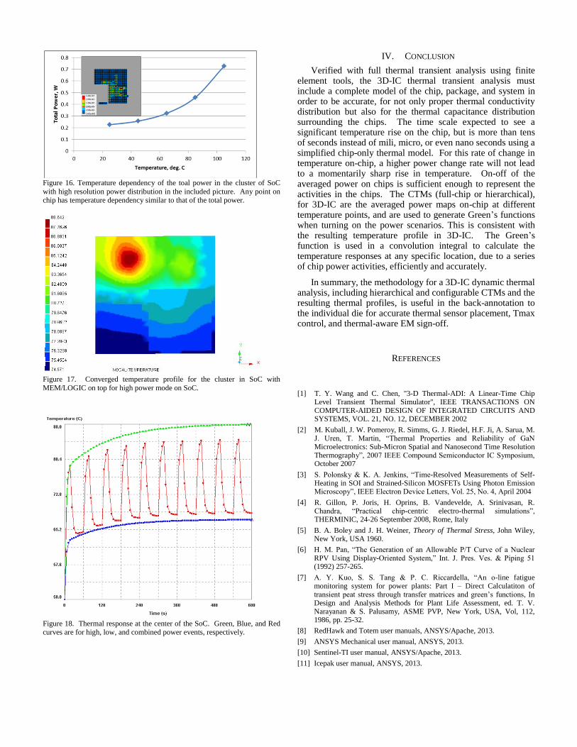
Figure 16. Temperature dependency of the toal power in the cluster of SoC
with high resolution power distribution in the included picture. Any point on chip has temperature dependency similar to that of the total power.
Figure 17. Converged temperature profile for the cluster in SoC with
MEM/LOGIC on top for high power mode on SoC.
Figure 18. Thermal response at the center of the SoC. Green, Blue, and Red curves are for high, low, and combined power events, respectively.
IV. CONCLUSION
Verified with full thermal transient analysis using finite element tools, the 3D-IC thermal transient analysis must include a complete model of the chip, package, and system in order to be accurate, for not only proper thermal conductivity distribution but also for the thermal capacitance distribution surrounding the chips. The time scale expected to see a significant temperature rise on the chip, but is more than tens of seconds instead of mili, micro, or even nano seconds using a simplified chip-only thermal model. For this rate of change in temperature on-chip, a higher power change rate will not lead to a momentarily sharp rise in temperature. On-off of the averaged power on chips is sufficient enough to represent the activities in the chips. The CTMs (full-chip or hierarchical), for 3D-IC are the averaged power maps on-chip at different temperature points, and are used to generate Green’s functions when turning on the power scenarios. This is consistent with the resulting temperature profile in 3D-IC. The Green’s function is used in a convolution integral to calculate the temperature responses at any specific location, due to a series of chip power activities, efficiently and accurately.
In summary, the methodology for a 3D-IC dynamic thermal analysis, including hierarchical and configurable CTMs and the resulting thermal profiles, is useful in the back-annotation to the individual die for accurate thermal sensor placement, Tmax control, and thermal-aware EM sign-off.
REFERENCES
[1] T. Y. Wang and C. Chen, "3-D Thermal-ADI: A Linear-Time Chip Level Transient Thermal Simulator", IEEE TRANSACTIONS ON COMPUTER-AIDED DESIGN OF INTEGRATED CIRCUITS AND SYSTEMS, VOL. 21, NO. 12, DECEMBER 2002
[2] M. Kuball, J. W. Pomeroy, R. Simms, G. J. Riedel, H.F. Ji, A. Sarua, M. J. Uren, T. Martin, “Thermal Properties and Reliability of GaN Microelectronics: Sub-Micron Spatial and Nanosecond Time Resolution Thermography”, 2007 IEEE Compound Semiconductor IC Symposium, October 2007
[3] S. Polonsky & K. A. Jenkins, “Time-Resolved Measurements of Self-Heating in SOI and Strained-Silicon MOSFETs Using Photon Emission Microscopy”, IEEE Electron Device Letters, Vol. 25, No. 4, April 2004
[4] R. Gillon, P. Joris, H. Oprins, B. Vandevelde, A. Srinivasan, R. Chandra, “Practical chip-centric electro-thermal simulations”, THERMINIC, 24-26 September 2008, Rome, Italy
[5] B. A. Boley and J. H. Weiner, Theory of Thermal Stress, John Wiley, New York, USA 1960.
[6] H. M. Pan, “The Generation of an Allowable P/T Curve of a Nuclear RPV Using Display-Oriented System,” Int. J. Pres. Ves. & Piping 51 (1992) 257-265.
[7] A. Y. Kuo, S. S. Tang & P. C. Riccardella, “An o-line fatigue monitoring system for power plants: Part I – Direct Calculatiton of transient peat stress through transfer matrices and green’s functions, In Design and Analysis Methods for Plant Life Assessment, ed. T. V. Narayanan & S. Palusamy, ASME PVP, New York, USA, Vol, 112, 1986, pp. 25-32.
[8] RedHawk and Totem user manuals, ANSYS/Apache, 2013.
[9] ANSYS Mechanical user manual, ANSYS, 2013.
[10] Sentinel-TI user manual, ANSYS/Apache, 2013.
[11] Icepak user manual, ANSYS, 2013.

[12] Bruce M. Guenin,"Simplified transient model for IC packages", Electronics Cooling Magazine, August 1st, 2002.
[13] S. Pan, N. Chang, and J. Zheng, "IC-PACKAGE THERMAL CO-ANALYSIS IN 3D IC ENVIRONMENT", InterPACK2011-52240, July 6-8, 2011, Portland, Oregon, USA.
[14] S. Pan, M. Ma, N. Chang, G. Shankaran, and M. Nagulapally, "Thermal Co-analysis of 3D-IC/Packages/System," 4-TA4, DesignCon2013, Santa Clara, CA, Jan. 29, 2013..


![[Elearnica.ir]-Bacterial Foraging Optimization Algorithm Theoretical Foundations Analysi](https://img.pdfslide.us/doc/110x75/55cf8aaa55034654898cc30c/elearnicair-bacterial-foraging-optimization-algorithm-theoretical-foundations.jpg)


![WP91 Lucia Montanaro Kosovo State Building Conundrum 3dic[1]](https://img.pdfslide.us/doc/110x75/577d27671a28ab4e1ea3d6e5/wp91-lucia-montanaro-kosovo-state-building-conundrum-3dic1.jpg)