Embed Size (px)
Citation preview
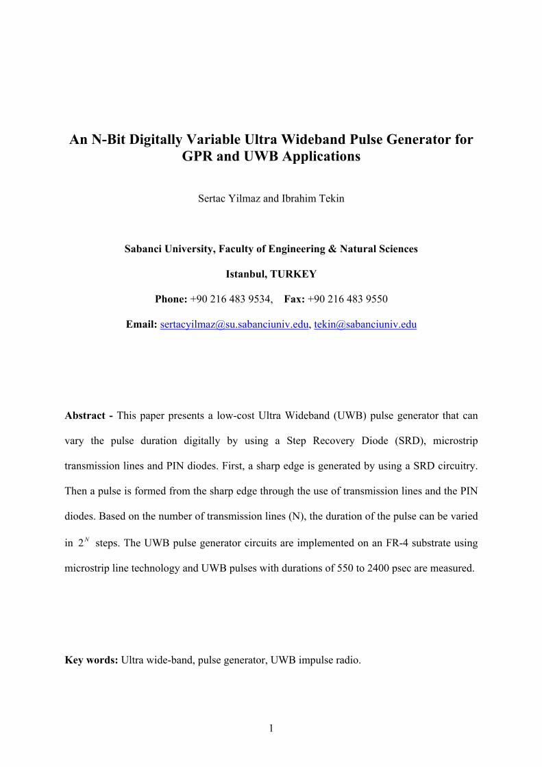
An N-Bit Digitally Variable Ultra Wideband Pulse Generator for GPR and UWB Applications
Sertac Yilmaz and Ibrahim Tekin
Sabanci University, Faculty of Engineering & Natural Sciences
Istanbul, TURKEY
Phone: +90 216 483 9534, Fax: +90 216 483 9550
Email: [email protected], [email protected]
Abstract - This paper presents a low-cost Ultra Wideband (UWB) pulse generator that can
vary the pulse duration digitally by using a Step Recovery Diode (SRD), microstrip
transmission lines and PIN diodes. First, a sharp edge is generated by using a SRD circuitry.
Then a pulse is formed from the sharp edge through the use of transmission lines and the PIN
diodes. Based on the number of transmission lines (N), the duration of the pulse can be varied
in steps. The UWB pulse generator circuits are implemented on an FR-4 substrate using
microstrip line technology and UWB pulses with durations of 550 to 2400 psec are measured.
N2
Key words: Ultra wide-band, pulse generator, UWB impulse radio.
1
Introduction
UWB technology has found military applications such as ground penetrating radar (GPR),
wall penetrating radar, secure communications and precision positioning/tracking [1, 2].
However, there is also a growing interest in commercial use of UWB technology such as in
Wireless Personal Area Networks (WPAN) [3, 4]. This interest has been the result of
increasing demand for much higher data rates on the order of hundreds of megabits since
future wireless networks requires very large transmission bandwidths to reach these data rates.
Currently, most wireless data technologies such as Bluetooth, IEEE 802.11b have baseband
signals up to tens of megabits, and the baseband signal is sent using an RF carrier, which is
basically a narrowband communication technique.
FCC recently allocated the frequency range from 3.1 to 10.6 GHz for UWB communications.
UWB signal is defined as the signal that has the bandwidth to center frequency ratio greater
than 0.25 or bandwidth of 500 MHz or higher. There are mainly two alternative ways of
UWB systems from the point of view of generating the UWB signal. One system is so called
the impulse radio in which ultra narrow pulses in picoseconds are generated and the generated
time pulses may span of a few GHz bandwidth. It is mostly preferred in the GPR and
precision positioning/tracking system. The other system is the multi-banded approach so that
multiple narrowband signals are generated independently and then combined to form the
larger bandwidth of UWB signal [5]. The multi-banded orthogonal frequency-division
multiplexing (OFDM) approach is used in the commercial UWB systems.
In the impulse GPRs, the pulse widths of the generated time pulses have influence on the
resolution of the radar. If the impulse radio is used as GPR to provide high penetration depth,
higher pulse durations are preferred; however, it also brings about low resolution. Decreasing
2
of the sounding pulse duration and increasing the resolution is considered as one of the most
promising ways for increase the quality of primary GPR data. However, excessively high
resolution can also have inverse effect. Rather, use of more durational sounding signals can
improve the primary GPR data [6]. Therefore, tuning the pulse width of the signal provides
more flexibility and improved performance in UWB application systems. Particularly, in
UWB ground penetrating radar, a digitally tunable pulse generator allows the pulse width to
be changed digitally to achieve varying penetration depths and resolution [7].
In this paper, a digitally tunable UWB pulse generator for an impulse type of pulse generator
is described. The pulse generator is realized with a simple circuitry by using Step Recovery
Diode (SRD), PIN diodes and transmission lines. These components are also employed in the
many equivalent basic UWB pulse generation circuits [8, 9]. The pulse generator as shown in
Figure 1 generates initial sharp edges by using a Step Recovery Diode (SRD) from the input
sinusoidal signal; then converts the sharp edges into short pulses with desired durations by
using parallel short-circuited stub with variable length. This variable length is obtained by
many PIN Diodes and transmission line sub-sections. The digitally tunable UWB pulse
generator has been designed and implemented using microstrip line technology and yielded
reasonable performance. Typical pulse durations varying from 550 to 1750 psec and from 900
to 2500 psec have been obtained experimentally for 2-bit and 4-bit pulse generator,
respectively. Experimental results are also duplicated using simulations based on Agilent
Advance Design System (ADS) platform.
N-Bit digitally tunable UWB pulse generator
N-bit digitally tunable UWB pulse generator is implemented with two main sub-circuits; Step
Recovery Diode (SRD) circuit and the Phase Shifter circuit as shown in Figure 1. The figure
3
shows the input step recovery diode circuit, phase shifter circuit with N PIN diodes and
transmission line sub-sections and the output load. The basic formation of an UWB pulse is
obtained first by creating a sharp edge by using SRD and then followed by the sharp edge
being splitted into two components and then followed through two different signal paths. One
signal component goes directly to the circuit output, the other component is delayed by the
phase shifter circuit and also the polarity of the pulse is reversed through the use of a short
circuit. The summation of these two components will yield the desired UWB pulse at the
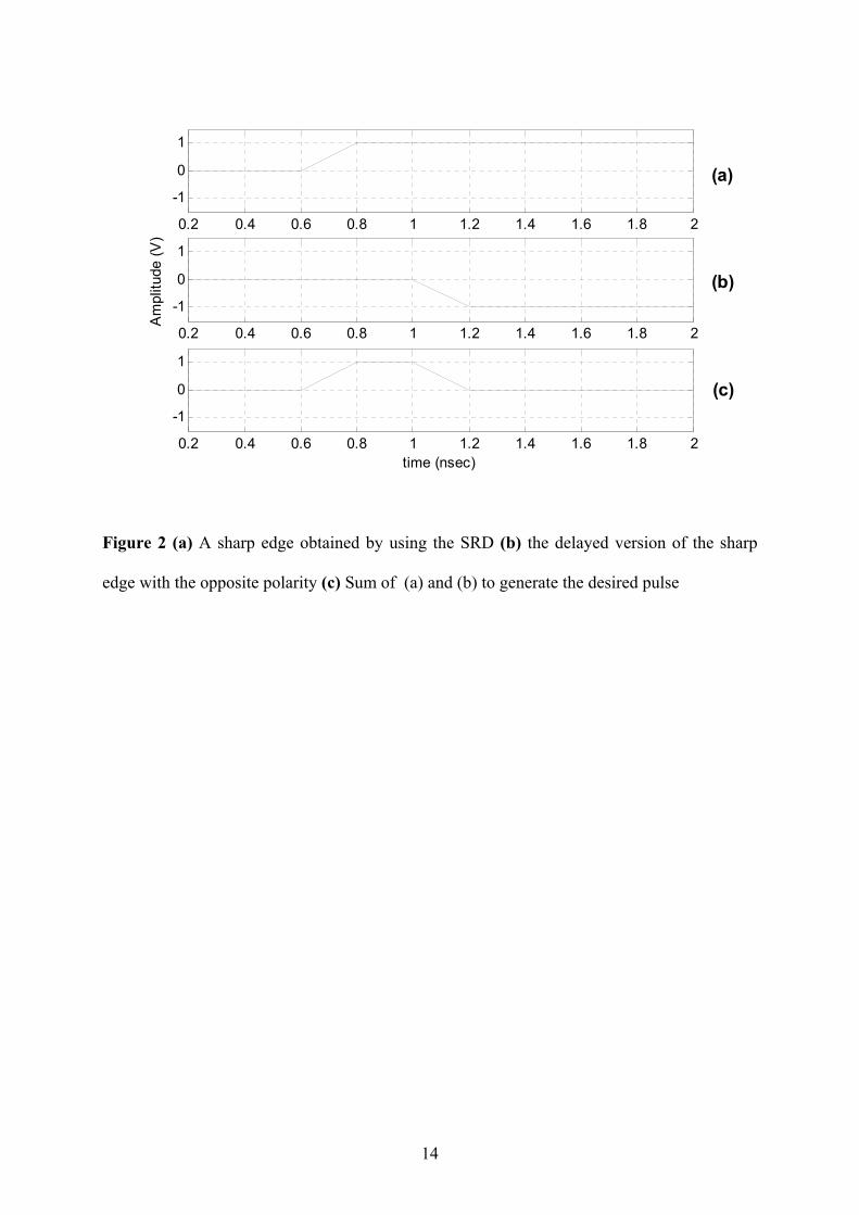
output as shown in the Figure 2. In the figure, generation of the pulse is mathematically
modeled. In Figure 2.a, it shows the generated sharp edge with 1 Volt amplitude and 200 psec
rise time by SRD. In Figure 2.b, the 400 psec delayed version of the sharp edge with the
opposite polarity is shown and the sum of the graphs 2.a and 2.b generates the desired pulse as
shown in Figure 2.c. Note that, the same circuitry can be used to obtain a Gaussian
Monocycle waveform, in other words; adding two mono pulses back to back with one of them
being with opposite polarity generates a Gaussian monocycle waveform.
Step recovery diodes (SRDs) have remained extremely useful in wave-shaping applications in
the last few decades since they were first presented. No other device rivals their combination
of fast switching speed and ease of use [10]. Figure 3 shows the typical circuit configurations
for SRD pulse sharpening. In both circuits, the SRD is initially biased with a constant forward
bias current IBIAS, which stores charge in the SRD. When the voltage source VIN rises, reverse
biasing the SRD, the SRD conducts for a short period of time, removing the stored charge.
This keeps the voltage across the diode very low. Then the stored charge is abruptly
exhausted, and the SRD switches to a high-impedance, high-voltage state, resulting in a
sharpening of the output voltage waveform. Therefore in the step recovery diode circuit, the
SRD generates a sharp edge on the order of picoseconds from a low frequency sinusoidal
signal applied to the input port of SRD diode circuit.
4
The phase shifter circuit is connected in parallel to the SRD circuit and the main purpose of
the phase shifter circuit is to delay the sharp edge generated by the SRD, and to reverse the
polarity of the delayed edge by a short circuit which terminates the phase shifter (or delay
line) circuit. Actually, phase shifter circuit is a true time delay (TTD) circuit. In addition to
SRD circuitry, phase shifter circuit implemented with microstrip lines constitutes the rest of
the UWB pulse circuit. A section of a phase shifter circuit includes a microstrip transmission
line, PIN diodes, RF chokes (LRF) and a DC blocking capacitor (CBL). Microstrip transmission
lines are planar transmission lines which are fabricated by photolithographic processes and
easily integrated with passive and active microwave devices. They are used as the delay
elements of the phase shifter circuit; therefore, the lengths and numbers of the transmission
lines are selected in accordance with the desired pulse widths since the transmission line
lengths determine the amount of time delay. Other important components of the phase shifter
circuit are PIN diodes. PIN diodes find applications as high-frequency switches for RF signals
up to 50 GHz. They contain an additional layer of an intrinsic (I-layer) or lightly doped
semiconductor sandwiched between highly doped p+ and n+ layers. In forward direction, the
diode behaves as if it possesses a variable resistance controlled by the applied current.
However, in reverse direction the lightly doped inner layer creates space charges whose extent
reaches the highly doped outer layers. This effect takes place even for small reverse voltages
and remains essentially constant up to high voltages, with the consequence that the diode
behaves similar to a dual plate capacitor [11]. The bias point setting required to operate the
PIN diode has to be provided through a DC circuit that must be separated from the RF signal
path. The DC isolation is achieved by a radio frequency coil (RFC) or RF choke, representing
a short circuit at DC and an open circuit at high frequency. Conversely, DC blocking
capacitors (CBL) represent an open circuit at DC and a short circuit at RF. Figure 4 shows a
5
typical switching circuit where the PIN diode is used in series connection. In the phase shifter
circuit, the PIN diodes are used as RF switch to control whether the signal goes through that
delay element or not. In each section, there are three PIN diodes. As shown in Figure 1, if the
series PIN 1 diode is forward-biased with positive bias voltage, then the PIN 2 and 3 are
reverse biased, and hence the RF signal reaches the point B from the point A over the PIN 1
diode. On the other hand, if the PIN 2 and 3 are forward biased with negative voltage, then the
PIN 1 diode is reverse-biased and the RF signal reaches the point B from the point A over the
transmission line, and is delayed by the transmission line length. Depending on the desired
pulse width, one or more phase shifter sections may be connected in series. All these phase
shifter sections can be capacitively coupled by using DC blocking capacitors connected
between the adjacent phase shifter sections. Various combinations of the PIN diodes can be
used to obtain different durations by using only N phase shifter sections. The series PIN
diodes to the transmission lines also avoids undesired reflections during the pulse generation.
N2
Simulation Results and Measurements
Both 2-section and 4-section versions of the N-bit digitally tunable UWB pulse generator
were first designed and simulated using Agilent Advanced Design System version 2003c to
compare their performances. The UWB pulse generator circuits were then implemented on the
FR-4 glass epoxy substrate with relative dielectric constant of 4.55 and thickness of 1.55 mm
as shown in Figure 5 and Figure 6. The SRDs used in the circuit are series MSD700-75 and
the PIN diodes are Ultra-Fast Switching series MMP7010-CS127 Low-High Power both
manufactured by Micrometrics Inc. To obtain the desired pulse widths at the outputs, two and
four sections are used in the phase shifter circuits of the pulse generators. In the 2-bit digitally
tunable UWB pulse generator, the transmission lines are implemented using microstrip line
technology so that the widths of the transmission lines are adjusted to 3 mm for matching the
6
transmission lines to the 50 Ohm at working frequencies and the lengths of the transmission
lines are selected as 3 and 6 cm to produce 200 and 400 psec delays, respectively. The lengths
of transmission lines are calculated by using Equations (1) and (2) given by
e
cpv
ε= (1)
where is the phase velocity in m/sec, c is the velocity of light and pv eε is the relative
dielectric constant of the material. Equation (2) relates the length of the transmission line to
the desired delay and phase velocity and it is given by
pvtl ×∆= (2)
where l is the length in meters and ∆t is the desired time delay in seconds.
In the 4-bit digitally tunable UWB pulse generator, the transmission lines are also
implemented using microstrip line technology, the widths of the transmission lines are
adjusted to 3 mm and the lengths of the transmission lines are selected as 0.75, 1.5, 3 and 6
cm to produce 50, 100, 200 and 400 psec delays, respectively.
The minimum pulse width that can be obtained is limited by the SRD’s maximum transition
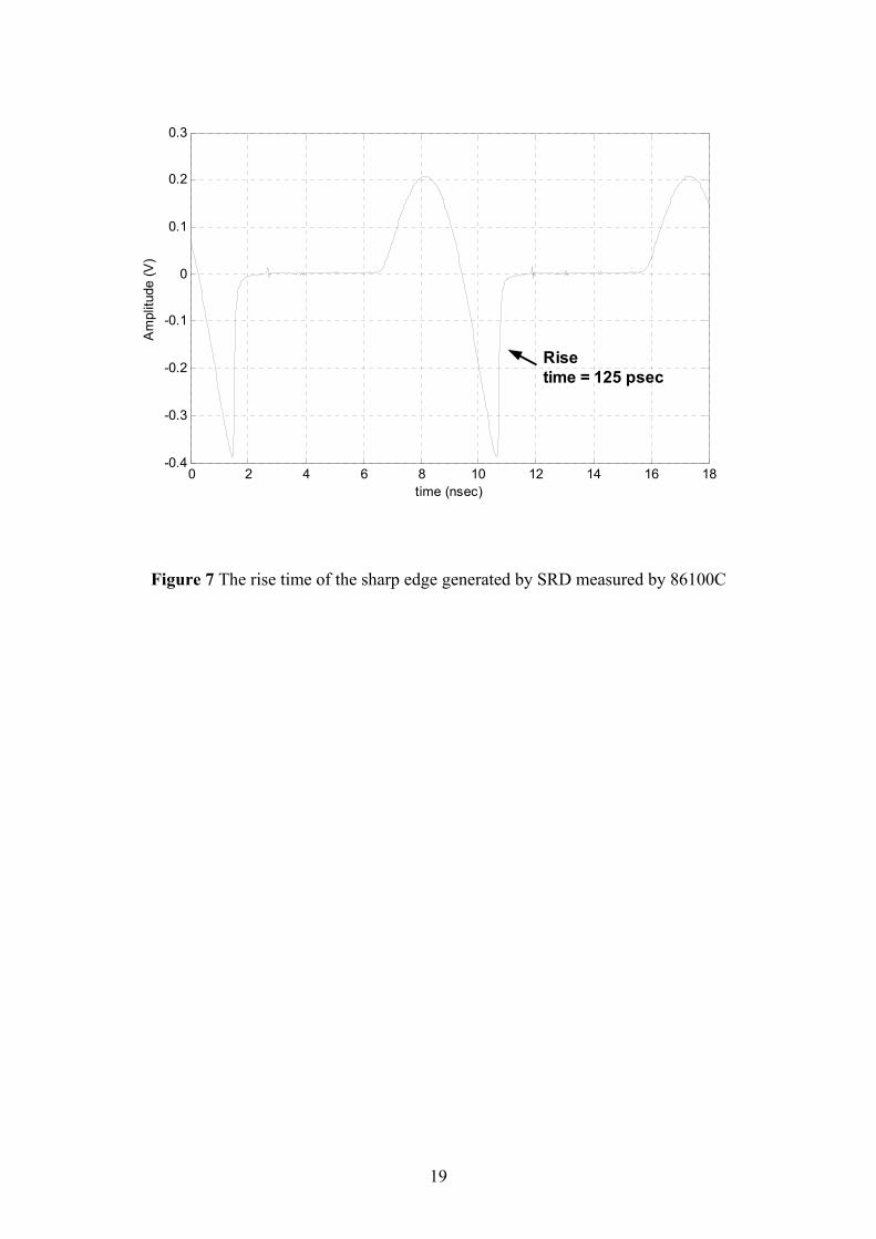
time which is measured by Agilent 8722ES Vector network analyzer around 125 psec. Figure
7 shows the phase measurement by the network analyzer. The slope of the phase measurement
is the rise time of the pulse, which is 125 psec. In addition, the group delays of the PIN diodes
and the dc blocking capacitors will also affect the pulse width. The group delay of one section
of the series PIN diode switch shown in the Figure 4 is measured with by network analyzer at
7
forward bias and gives rise to a time delay of 110 psec which can be calculated from the
Figure 8 as slope of the phase component of the reflection coefficient, . Note that the
overall pulse width is affected by twice the amount of group delay of the PIN diodes and the
dc blocking capacitors since the UWB pulse goes over the PIN diodes and then reflected by
the short circuit, and goes over the PIN diodes once again to reach the load. Therefore, the
possible shortest pulse width durations are around 550 and 900 psec for 2-bit and 4-bit pulse
generator, respectively; only including the offset delay of SRDs’ maximum transition times
and the group delays of PIN diodes and DC blocking capacitors. The other possible pulse
durations of the generator are given in the Table 1 and Table 2 with their digital codes.
11S
The ADS simulated output pulses of the 2-Bit digitally tunable UWB pulse generator are
shown in Figure 9. The pulse width range from 550 psec to 1750 psec with steps of 400 psec,
which corresponds to frequency bandwidth of 550 MHz to 2 GHz. Amplitude of the pulse
output is around 400 mV when the applied input has a peak of 1.4 V at a pulse repetition
frequency of 20 MHz. Also, note that the residual of the 20 MHz input signal around 28-31
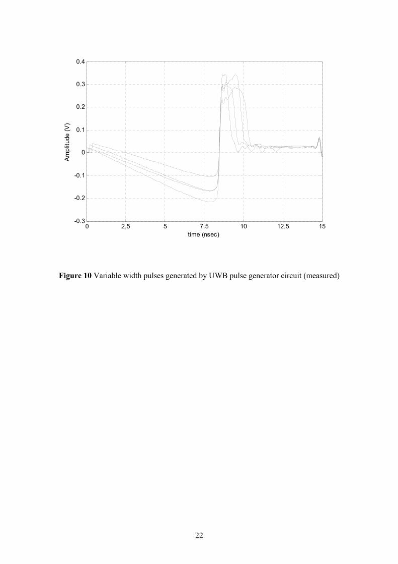
nsec which can easily be removed by a simple high pass filter. Measured UWB pulses are
shown in Figure 10, where the different possible combinations are plotted on the same graph.
The pulse amplitudes are around 300 mV for an applied signal of 1.4 V for the same
frequency of 20 MHz. Measurements are done with Agilent 86100C Digital Communication
Analyzer. The pulse widths are also in very good agreement with the simulations for 550 psec
to 1750 psec duration pulses.
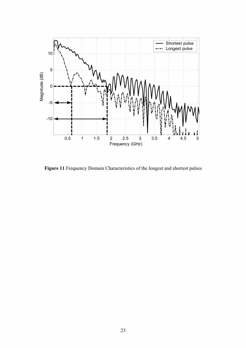
Also, the frequency domain characteristics of the output pulses of 2-bit pulse generator are
obtained by taking the Fourier transform of the measured pulses in time domain. The
frequency domain characteristics of the longest and shortest pulses are shown in Figure 11,
8
where the longest pulse has a first null bandwidth of 600 MHz, and the shortest pulse has first
null bandwidth of 1800 MHz, respectively.
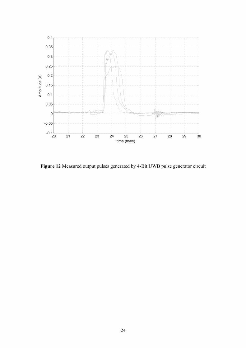
The measured output pulse widths for 4-bit pulse generator range from 900 psec to 2400 psec
with steps of 100 psec, which corresponds to bandwidth of 400 MHz to 1.1 GHz. In the
Figure 12, the shortest, the longest and the other two time pulses among 16 output pulses are
plotted on the same graph. Amplitude of the pulse output is around 300 mV when the applied
input signal has a peak of 1.4 V at a frequency of 20 MHz. The output pulse of the generator
can be easily used in and improve the performance of UWB GPR systems since most GPR
systems are designed to work between 0.1 and 1.5 GHz [12, 13].
Also, one should note that the resolution of the pulse generator increases when the numbers of
phase shifter sections are increased; however, this limits the frequency bandwidth since the
group delays of the PIN diodes and dc blocking capacitors increase as more sections are
placed into the circuitry. Therefore, there is a trade off between the frequency bandwidth and
the resolution that can be obtained.
Conclusion
In this paper, an UWB signal generator for an impulse type of pulse generator is described. 2-
section and 4-section versions of N-Bit digitally tunable UWB pulse generator using SRD,
microstrip line delay lines and PIN diodes are presented. The simulated and measured pulse
widths are in agreement and the pulse width changes from 550 psec (~2 GHz bandwidth) to
1750 psec (~550 MHz bandwidth) for 2-section version and changes from 900 psec (~1.1
GHz bandwidth) to 2400 psec (~450 MHz bandwidth) for 4-section version, which can be
considered as an UWB pulse. The minimum pulse width is determined by the transition time
9
of the employed SRD and the group delays of the PIN diodes and DC blocking capacitors
changed with the number of phase shifter sections. Also, the monocycle type pulses can be
easily obtained by using the similar circuitry which is used to obtain the UWB pulse. The
circuitry is low-cost, can be easily used in GPR, UWB radar, UWB positioning applications.
References
[1] H.L. Bertoni, L. Carin and L.B. Felsen, editors, “Ultra-Wideband short pulse
electromagnetic”, 1992, New York, Kluwer Publications.
[2] C.L. Bennett and G.F. Ross, “Time-domain electromagnetic and its applications”,
Proceedings of IEEE, Vol. 66, No.3, pp. 29-318, 1978.
[3] Ultra Wideband Tutorial, “IEEE P802.15 Working group for WPAN document”, doc.
No. IEEE 802.15-00/083r0, March 2000.
[4] J. Foerster and et. Al, “Ultra-Wideband Technology for Short- or Medium Range
Wireless Communications”, Intel Technology Journal Q2, 2001.
[5] “Understanding UWB”, IEEE P802.15 working group document, doc. No. IEEE 802.15-
03/157r0, March 2003.
[6] Pochanin, G.P., “Problems and promising lines of development of UWB ground
penetrating radiolocation”, Ultrawideband and Ultrashort Impulse Signals, 2004 Second
International Workshop 19-22 Sept. 2004 Page(s):61 – 66.
[7] J. Han and C. Nguyen, “Ultra-Wideband Electronically Tunable Pulse Generators”, IEEE
Mıcrowave And Wıreless Components Letters, Vol. 14, No. 3, March 2004.
[8] J. S. Lee, Cam Nguyen, Scullion T., “A novel, compact, low-cost, impulse ground-
penetrating radar for nondestructive evaluation of pavements”, IEEE Transactions on
Instrumentation and Measurement, Volume: 53, Issue: 6, Dec. 2004.
10
[9] J. Ha, C. Nguyen, “A new ultra-wideband, ultra-short monocycle pulse generator with
reduced ringing”, IEEE Microwave and Wireless Components Letters, Volume:
12, Issue: 6, June 2002.
[10] M. J. Chudobiak, “New Approaches For Designing High Voltage, High Current Silicon
Step Recovery Diodes for Pulse Sharpening Applications”, PhD Thesis.
[11] R. Ludwig, P. Bretchko, “RF Circuit Design Theory and Applications”, New Jersey,
Prentice Hall Inc., 2000.
[12] Young-Jin Park, Sung-Bae Cho, Kwan-Ho Kim, Dong-Gi Youn, “Development of an
ultra wideband ground penetrating radar (UWB GPR) for nondestructive testing of
underground objects”, IEEE Antennas and Propagation Society Symposium, 2004,
Volume 2, 20-25 June 2004 Page(s):1279 - 1282 Vol.2.
[13] U. Uschkerat, “Comparing UWB GPR measurements and simulation of simple shaped
buried targets”, Detection of Abandoned Land Mines, 1998. Second International
Conference on the (IEE Conf. Publ. No. 458) 12-14 Oct. 1998 Page(s):41 – 44.
11
List of Figures
Figure 1 Schematic of the N-Bit digitally tunable pulse generator.
Figure 2 (a) A sharp edge obtained by using the SRD (b) the delayed version of the sharp edge with the opposite polarity (c) Combined (a) and (b) to generate the desired pulse.
Figure 3 Standard step recovery diode pulse sharpening circuits.
Figure 4 Switching circuit with biased PIN diode in series configuration.
Figure 5 Photograph of the 2-bit digitally tunable UWB pulse generator.
Figure 6 Photograph of the 4-bit digitally tunable UWB pulse generator.
Figure 7 The rise time of the sharp edge generated by SRD.
Figure 8 Phase of versus frequency graph of the series PIN-diodes. 11S
Figure 9 The ADS simulated pulses of 2-Bit digitally tunable UWB pulse generator.
Figure 10 Variable width pulses generated by 2-BitUWB pulse generator circuit.
Figure 11 Frequency Domain Characteristics of the longest and shortest pulses
Figure 12 Measured output pulses generated by 4-Bit UWB pulse generator circuit.
List of Tables
Table 1 Pulse durations of 2-bit digitally tunable pulse generator
Table 2 Pulse durations of 4-bit digitally tunable pulse generator
12
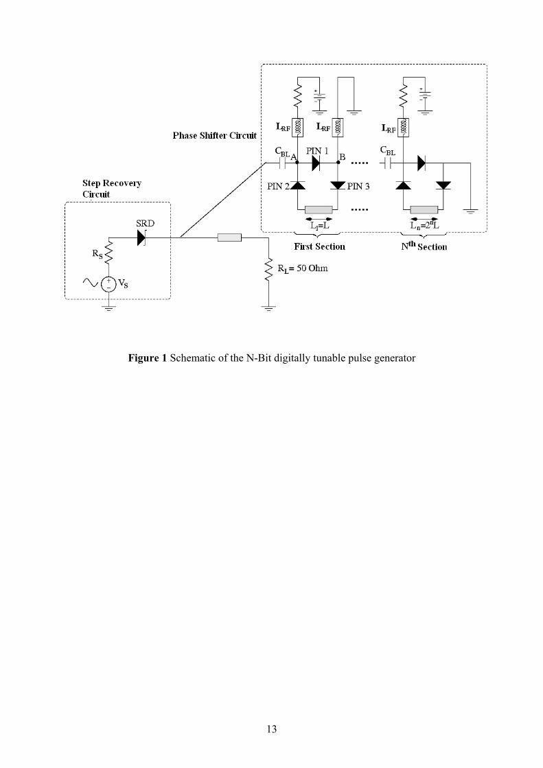
Figure 1 Schematic of the N-Bit digitally tunable pulse generator
13
0.2 0.4 0.6 0.8 1 1.2 1.4 1.6 1.8 2
-1
0
1
0.2 0.4 0.6 0.8 1 1.2 1.4 1.6 1.8 2
-1
0
1
Am
plitu
de (V
)
0.2 0.4 0.6 0.8 1 1.2 1.4 1.6 1.8 2
-1
0
1
time (nsec)
(a)
(b)
(c)
Figure 2 (a) A sharp edge obtained by using the SRD (b) the delayed version of the sharp
edge with the opposite polarity (c) Sum of (a) and (b) to generate the desired pulse
14
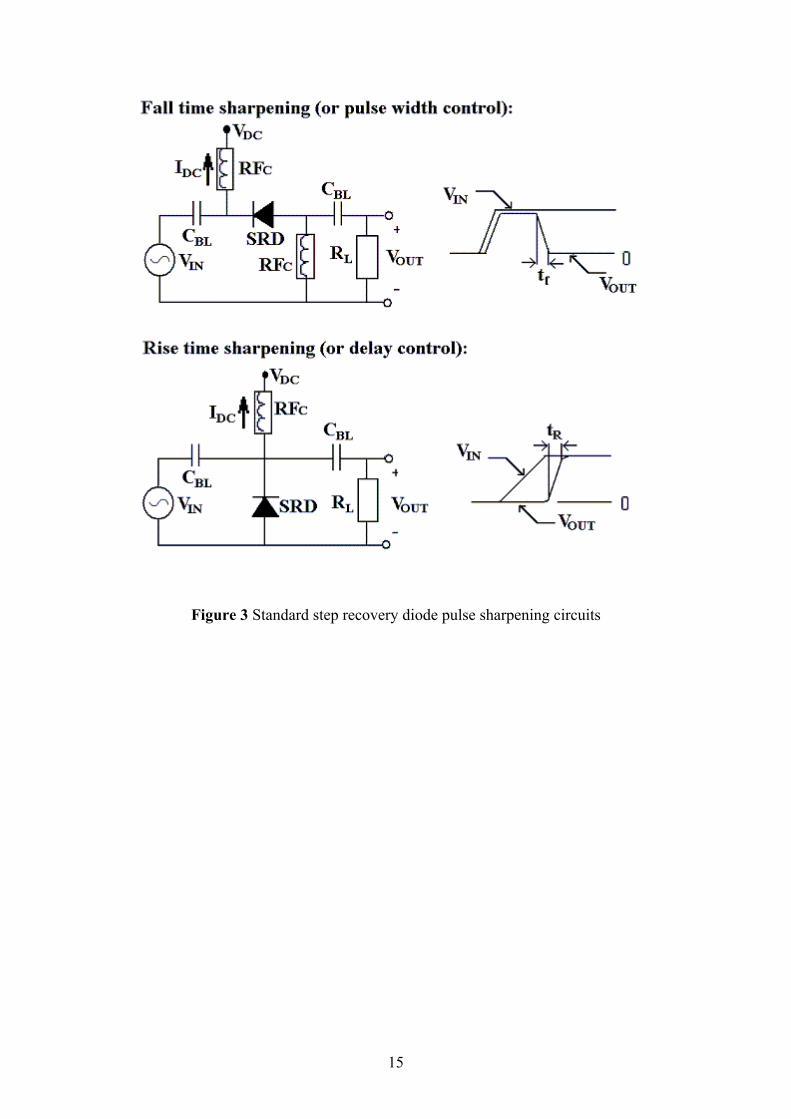
Figure 3 Standard step recovery diode pulse sharpening circuits
15

Figure 4 Switching circuit with biased PIN diode in series configuration
16
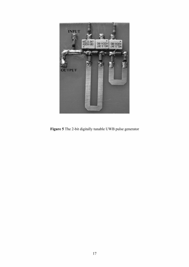
Figure 5 The 2-bit digitally tunable UWB pulse generator
17
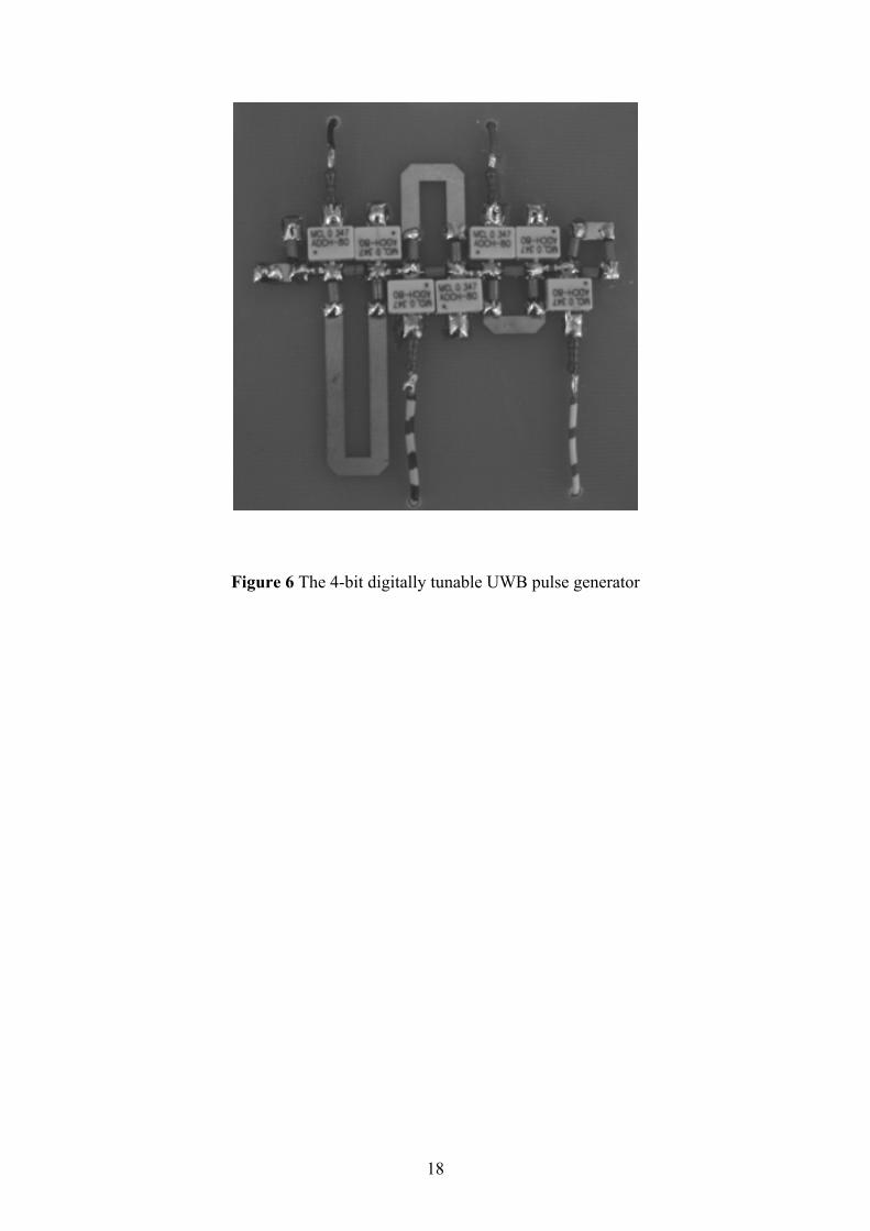
Figure 6 The 4-bit digitally tunable UWB pulse generator
18
0 2 4 6 8 10 12 14 16 18-0.4
-0.3
-0.2
-0.1
0
0.1
0.2
0.3
time (nsec)
Am
plitu
de (V
)
Risetime = 125 psec
Figure 7 The rise time of the sharp edge generated by SRD measured by 86100C
19

0 0.5 1 1.5 2 2.5 3 3.5 4 4.5 5
-180
-150
-100
-50
0
50
100
150
180
Frequency (GHz)
Pha
se (d
eg)
Group Delay = 110 psec
Figure 8 Phase of versus frequency graph of the series PIN-diodes measured by 8722ES 11S
20
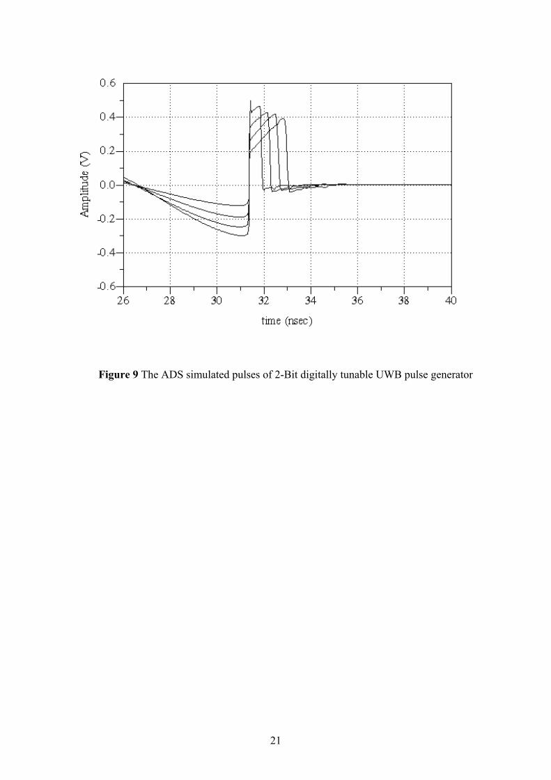
Figure 9 The ADS simulated pulses of 2-Bit digitally tunable UWB pulse generator
21
0 2.5 5 7.5 10 12.5 15-0.3
-0.2
-0.1
0
0.1
0.2
0.3
0.4
time (nsec)
Am
plitu
de (V
)
Figure 10 Variable width pulses generated by UWB pulse generator circuit (measured)
22
0.5 1 1.5 2 2.5 3 3.5 4 4.5 5
-10
-5
0
5
10
Frequency (GHz)
Mag
nitu
de (d
B)
Shortest pulseLongest pulse
Figure 11 Frequency Domain Characteristics of the longest and shortest pulses
23
20 21 22 23 24 25 26 27 28 29 30-0.1
-0.05
0
0.05
0.1
0.15
0.2
0.25
0.3
0.35
0.4
time (nsec)
Am
plitu
de (V
)
Figure 12 Measured output pulses generated by 4-Bit UWB pulse generator circuit
24
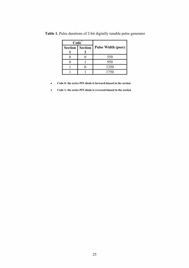
Table 1. Pulse durations of 2-bit digitally tunable pulse generator
Code*
Section 1
Section2
Pulse Width (psec)
0 0 550 0 1 950 1 0 1350 1 1 1750
• Code 0: the series PIN diode is forward-biased in the section
• Code 1: the series PIN diode is reversed-biased in the section
25
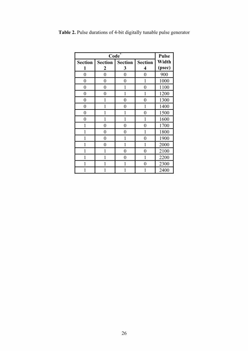
Table 2. Pulse durations of 4-bit digitally tunable pulse generator
Code*
Section 1
Section2
Section3
Section4
Pulse Width (psec)
0 0 0 0 900 0 0 0 1 1000 0 0 1 0 1100 0 0 1 1 1200 0 1 0 0 1300 0 1 0 1 1400 0 1 1 0 1500 0 1 1 1 1600 1 0 0 0 1700 1 0 0 1 1800 1 0 1 0 1900 1 0 1 1 2000 1 1 0 0 2100 1 1 0 1 2200 1 1 1 0 2300 1 1 1 1 2400
26