Embed Size (px)
Citation preview
Pulse-Based Ultra-WidebandTransmitters for Digital Communication
Ph.D. Thesis DefenseDavid Wentzloff
Thesis Committee:Prof. Anantha Chandrakasan (Advisor)
Prof. Joel DawsonProf. Charles Sodini
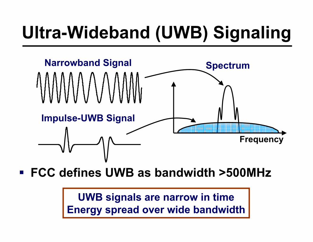
Ultra-Wideband (UWB) Signaling
FCC defines UWB as bandwidth >500MHz
Narrowband Signal
Impulse-UWB Signal
Frequency
UWB signals are narrow in timeEnergy spread over wide bandwidth
Spectrum
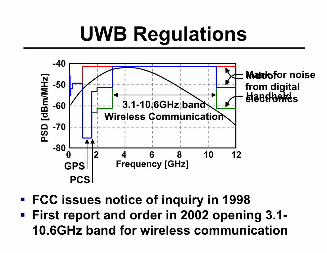
UWB Regulations
FCC issues notice of inquiry in 1998First report and order in 2002 opening 3.1-10.6GHz band for wireless communication
0 2 4 6 8 10 12-80
-70
-60
-50
-40
Frequency [GHz]
PSD
[dB
m/M
Hz]
PCSGPS
3.1-10.6GHz bandWireless Communication
Indoor
Handheld
Mask for noisefrom digitalelectronics
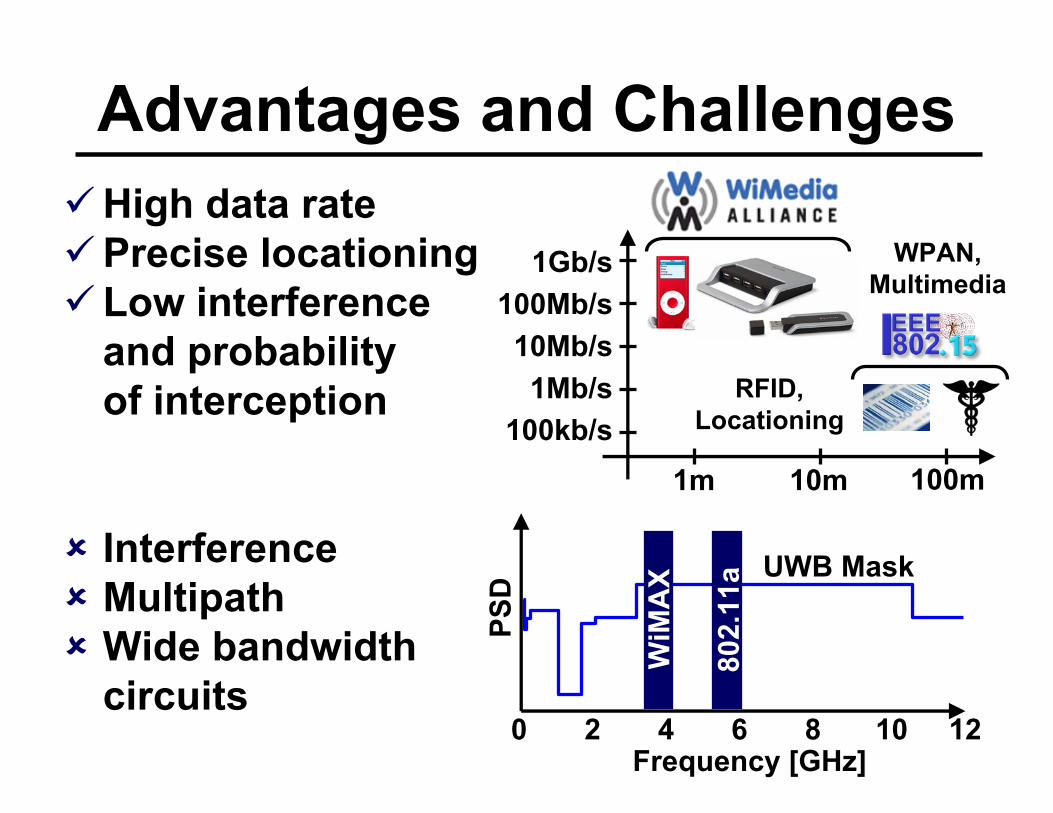
Advantages and ChallengesHigh data ratePrecise locationingLow interferenceand probabilityof interception
InterferenceMultipathWide bandwidth circuits
PSD
0 2 4 6 8 10 12Frequency [GHz]
802.
11a
WiM
AX UWB Mask
1m 10m 100m
1Gb/s100Mb/s10Mb/s1Mb/s RFID,
Locationing
WPAN,Multimedia
100kb/s

OutlineHigh data rate transmitter– Gaussian pulse shaping
Variable low data rate transmitter– All-digital architecture
Conclusions and future directions
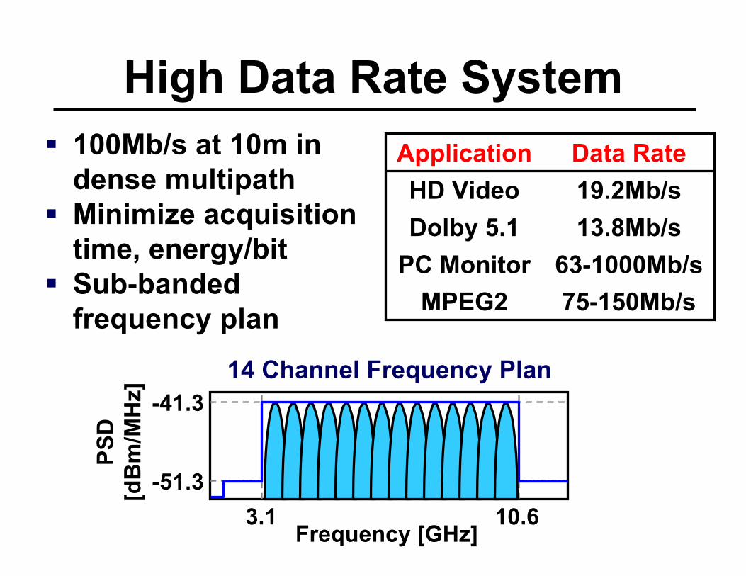
High Data Rate System100Mb/s at 10m in dense multipathMinimize acquisition time, energy/bitSub-banded frequency plan
14 Channel Frequency Plan
PSD
[dB
m/M
Hz]
3.1 10.6-51.3
-41.3
Frequency [GHz]
Data RateApplication
75-150Mb/sMPEG263-1000Mb/sPC Monitor
13.8Mb/sDolby 5.119.2Mb/sHD Video
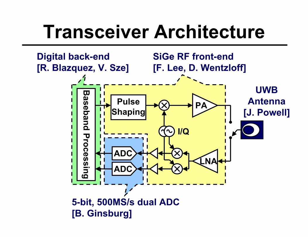
Transceiver Architecture
5-bit, 500MS/s dual ADC[B. Ginsburg]
Pulse Shaping
LNA
PA
I/Q
Digital back-end[R. Blazquez, V. Sze]
SiGe RF front-end[F. Lee, D. Wentzloff]
Baseband Processing
ADC
ADC
UWB Antenna
[J. Powell]
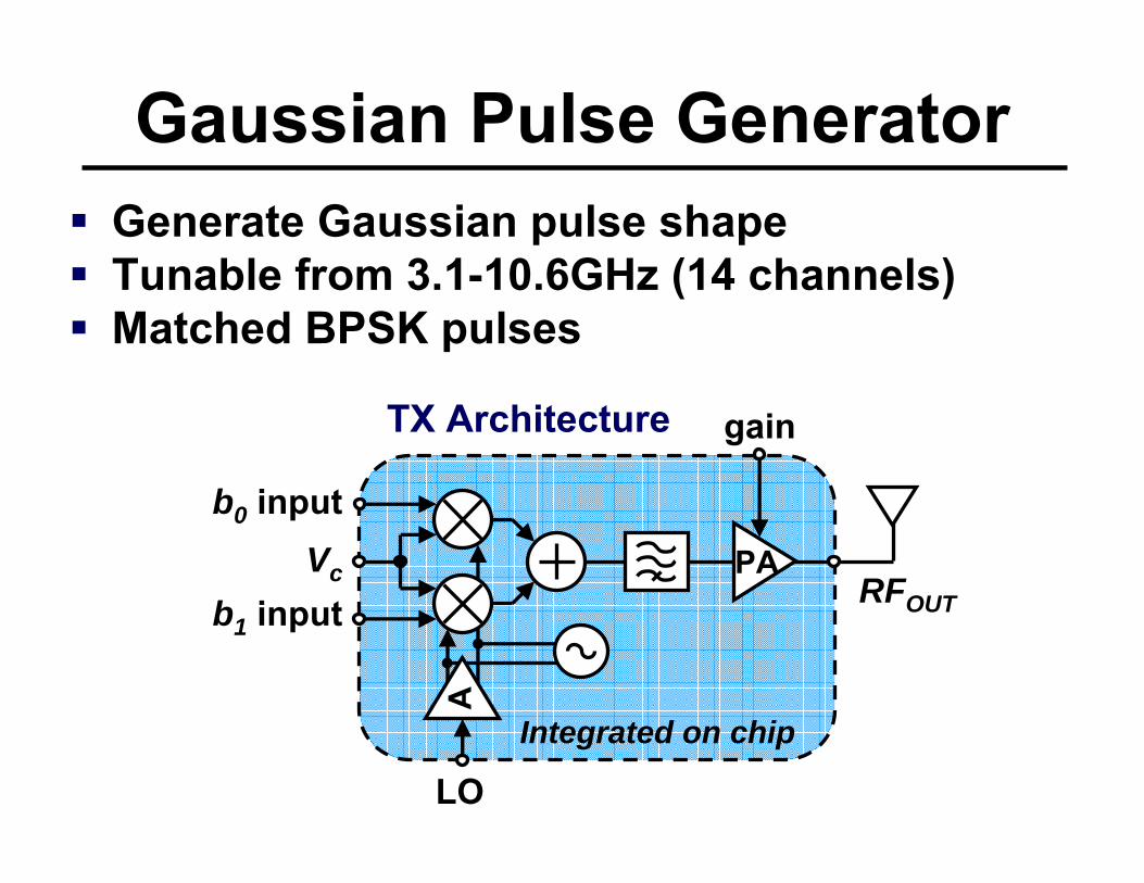
Gaussian Pulse GeneratorGenerate Gaussian pulse shapeTunable from 3.1-10.6GHz (14 channels)Matched BPSK pulses
Integrated on chip
LO
PA
b0 input
b1 inputVc
gainTX Architecture
RFOUT
A
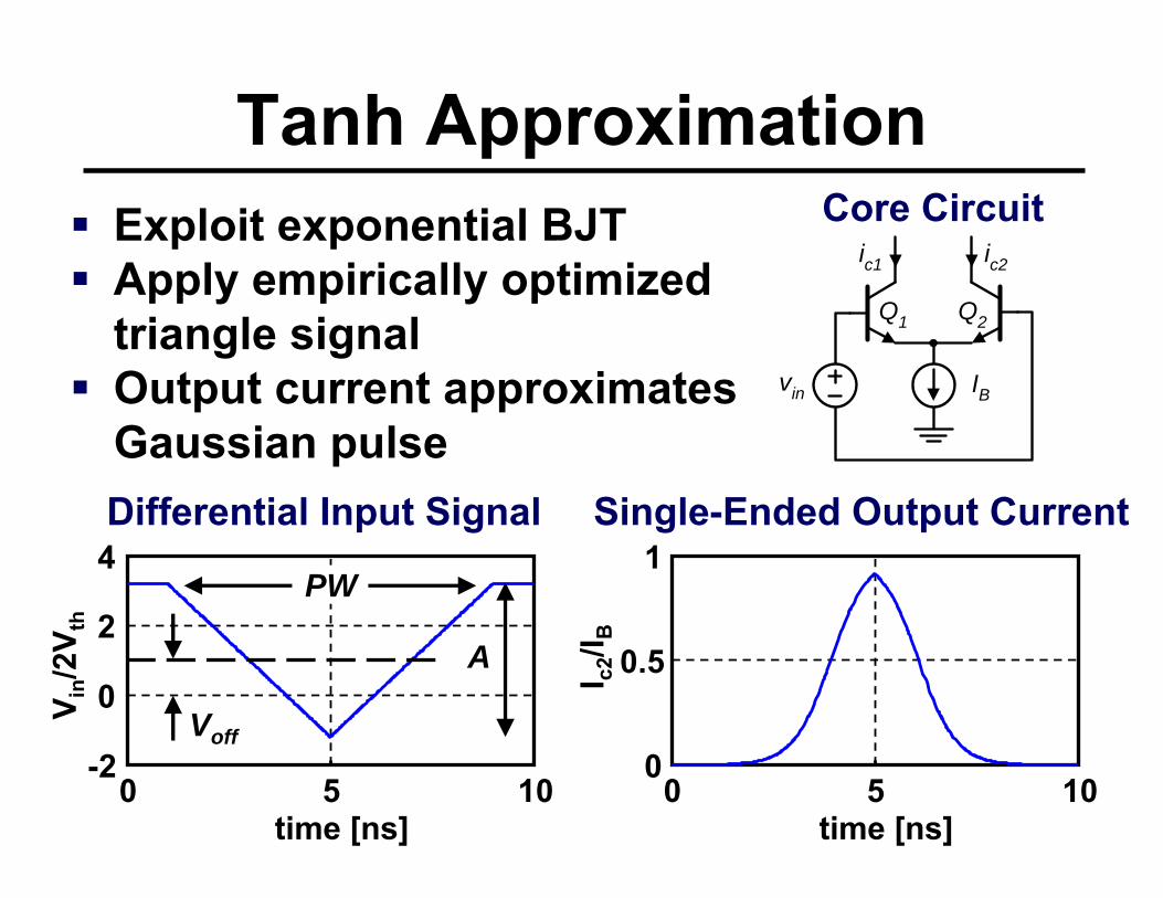
Tanh ApproximationExploit exponential BJTApply empirically optimized triangle signalOutput current approximates Gaussian pulse
IBvin
ic2ic1
Q1 Q2
0 5 100
0.5
1
time [ns]0 5 10
-2
0
2
4
time [ns]
PW
A
Voff
Differential Input Signal Single-Ended Output Current
Core Circuit
I c2/I B
V in/2
V th
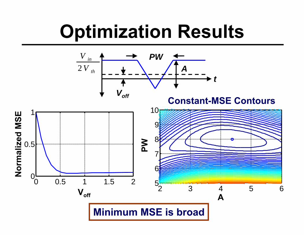
0 0.5 1 1.5 20
0.5
1
Voff
Nor
mal
ized
MSE
2 3 4 5 65
6
7
8
9
10
A
PW
Optimum for σ=1
Optimization Results
Minimum MSE is broad
Voff
PWAth
in
VV2
t
Constant-MSE Contours
A
PW
Voff
Nor
mal
ized
MSE

Optimized Pulse
-4 -2 0 2 40
0.2
0.4
0.6
0.8
1
1.2
Normalized time
Nor
mal
ized
am
plitu
de [V
]
TanhGauss
-4 -2 0 2 4-60-50-40-30-20-10
010
Normalized frequencyN
orm
aliz
ed a
mpl
itude
[dB
]
TanhGauss
1.7% maximum in-band errorbetween Tanh and Gaussian pulse
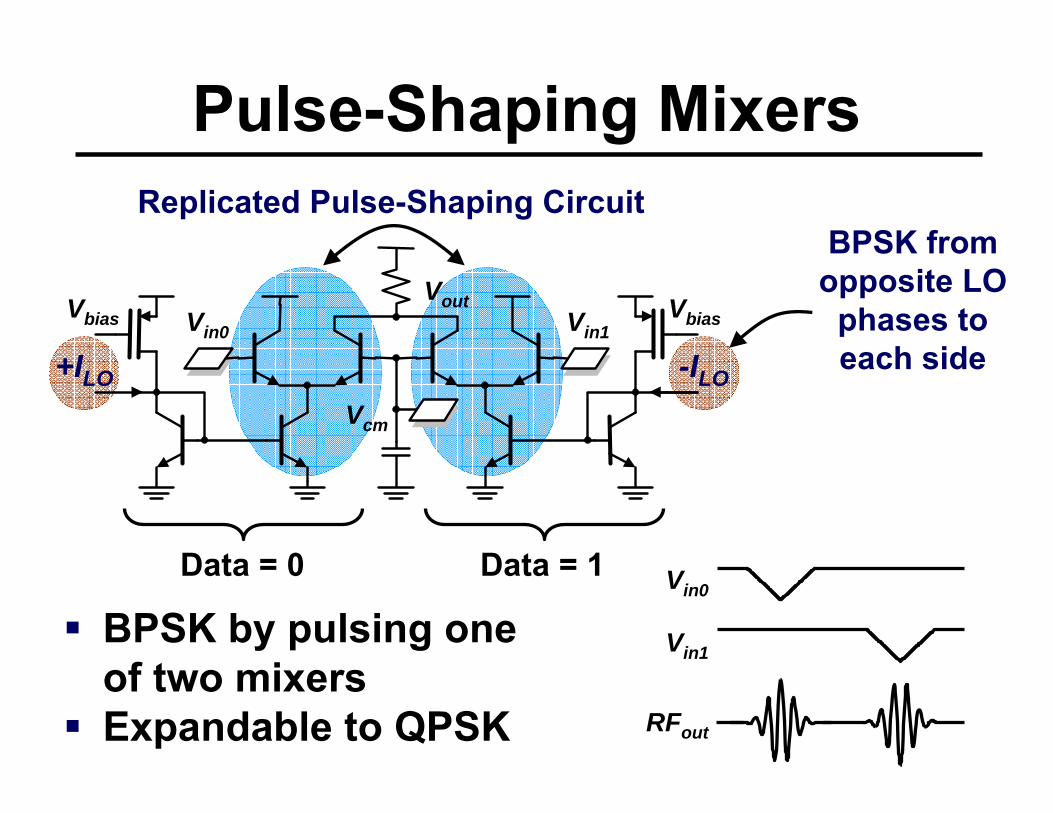
Pulse-Shaping Mixers
BPSK by pulsing one of two mixersExpandable to QPSK
Replicated Pulse-Shaping Circuit BPSK from
opposite LOphases toeach side
Data = 0 Data = 1
Vin0
-ILO+ILO
Vin1
Vin0
Vout
RFout
Vin1
Vcm
VbiasVbias
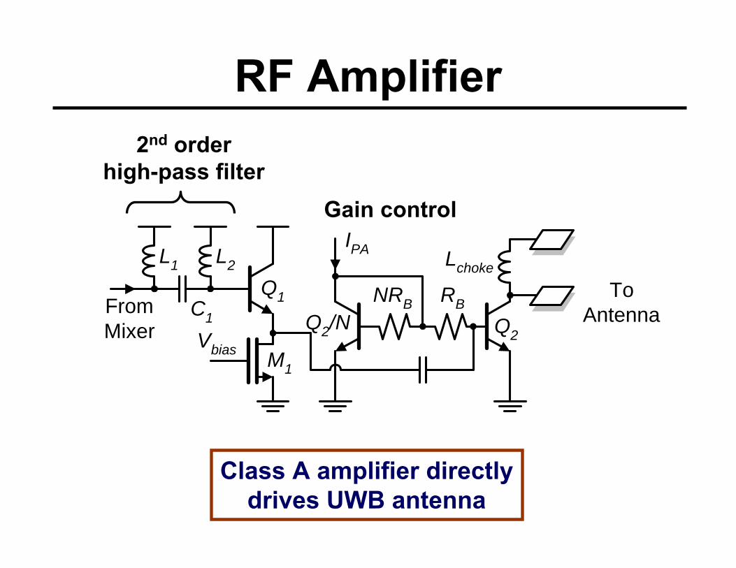
RF Amplifier
L1 L2
C1
Q1
M1
Vbias
FromMixer
IPA
Q2
RBNRBQ2/N
Lchoke
ToAntenna
2nd orderhigh-pass filter
Gain control
Class A amplifier directlydrives UWB antenna
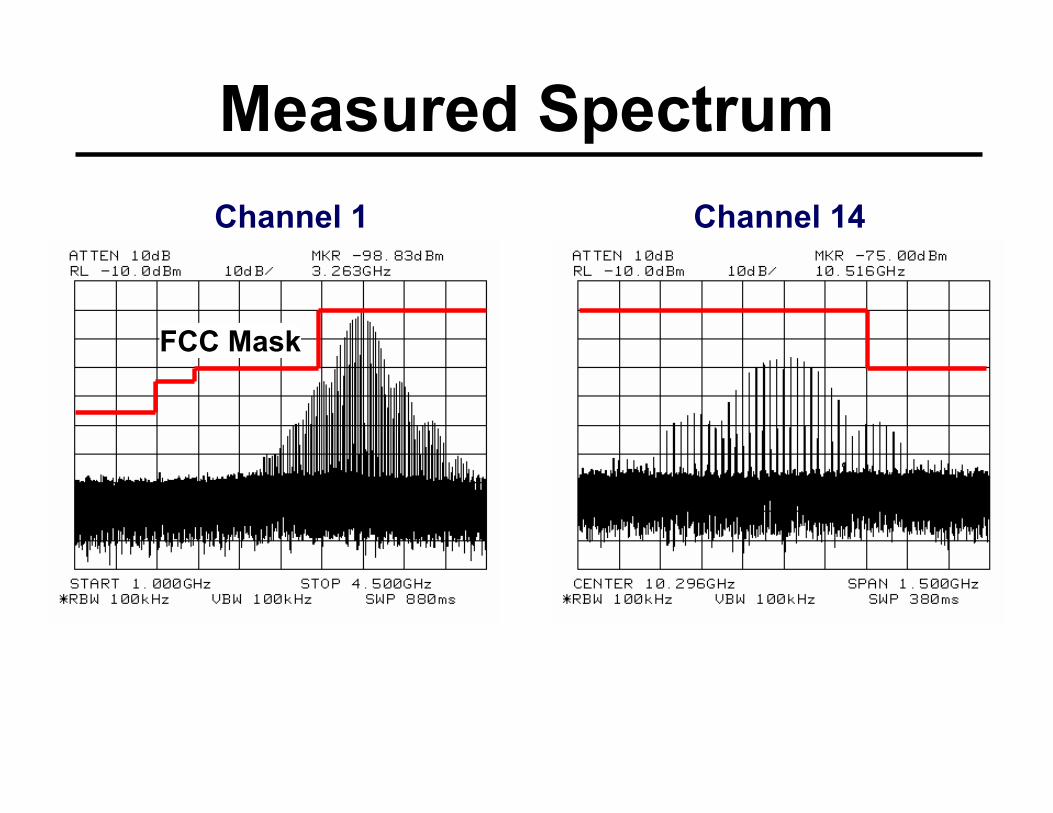
Measured SpectrumChannel 1 Channel 14
FCC Mask

BPSK Matching
Measured matching using on-chip VCOComparison to ideal Tanh response
-0.2 -0.15 -0.1 -0.05 0 0.05 0.1-40
-30
-20
-10
0
Differential input voltage [V]
RF
outp
ut p
ower
[dB
m]
Positive pulseNegative pulseIdeal Tanh Finite LO
feedthrough
Ideal Tanh Pulse
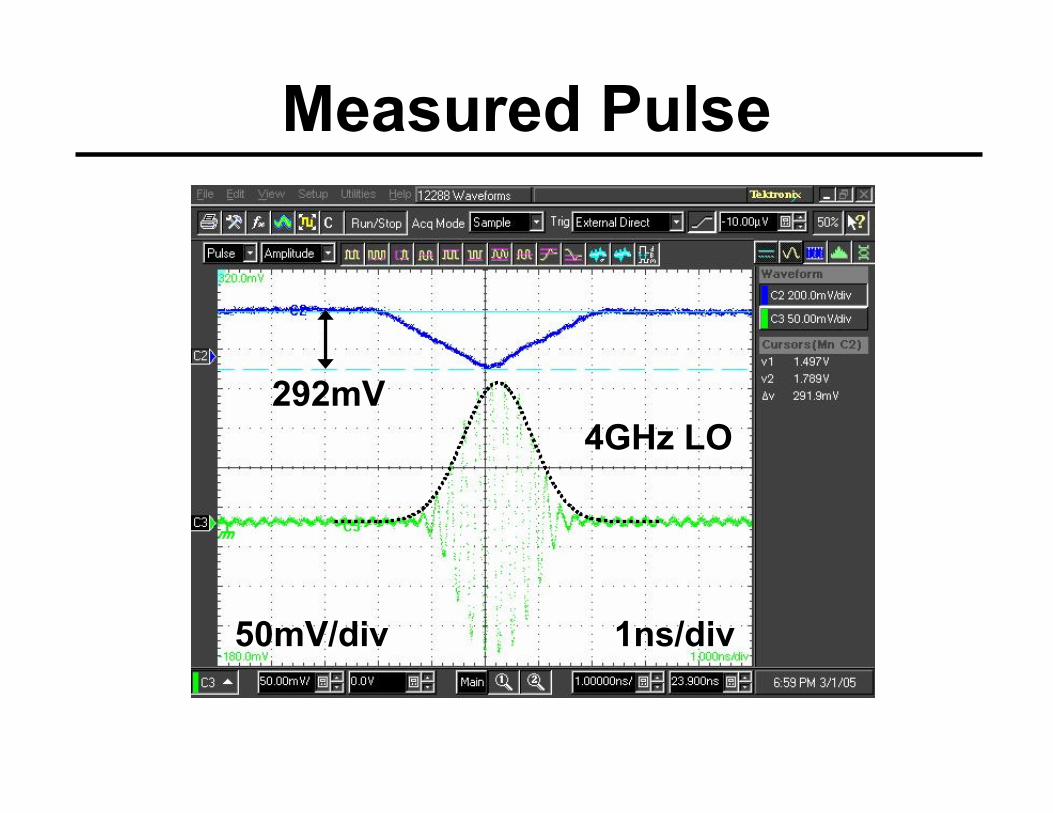
Measured Pulse
1ns/div50mV/div
292mV4GHz LO
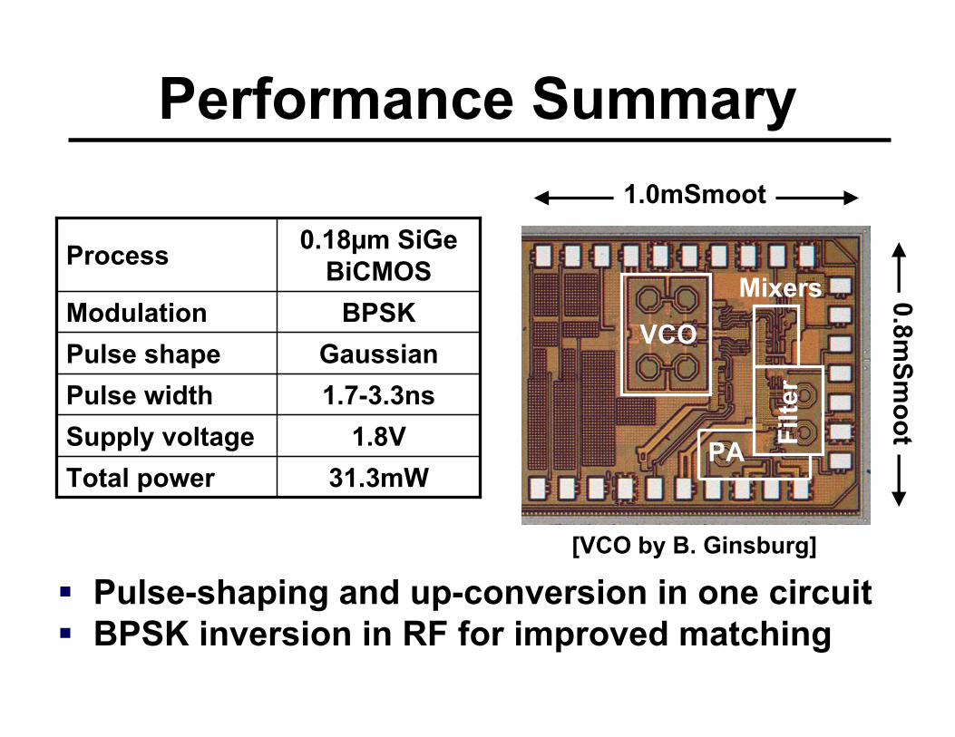
Performance Summary
Pulse-shaping and up-conversion in one circuitBPSK inversion in RF for improved matching
0.8mSm
oot
1.0mSmoot0.18µm SiGe
BiCMOSProcess
31.3mWTotal power1.8VSupply voltage
1.7-3.3nsPulse widthGaussianPulse shape
BPSKModulation
Filte
r
Mixers
PA
VCO
[VCO by B. Ginsburg]
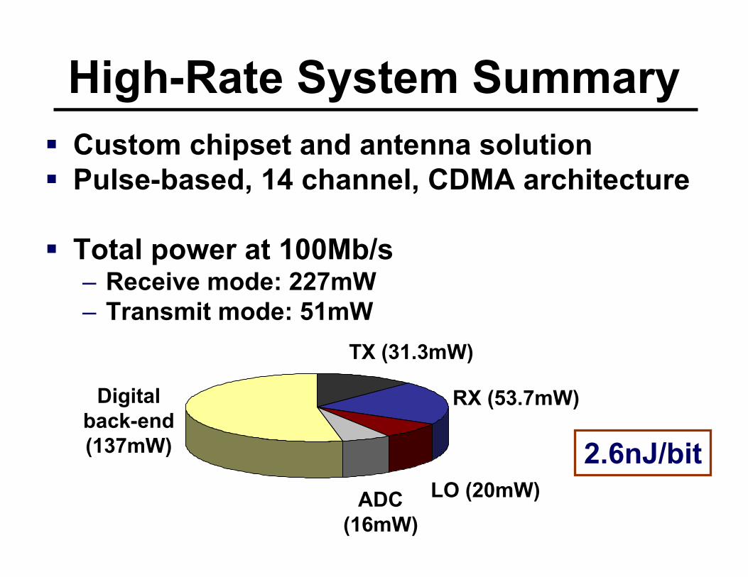
High-Rate System SummaryCustom chipset and antenna solutionPulse-based, 14 channel, CDMA architecture
Total power at 100Mb/s– Receive mode: 227mW– Transmit mode: 51mW
2.6nJ/bit
Digitalback-end(137mW)
ADC(16mW)
LO (20mW)
RX (53.7mW)
TX (31.3mW)
OutlineHigh data rate transmitter– Gaussian pulse shaping
Variable low data rate transmitter– All-digital architecture
Conclusions and future directions
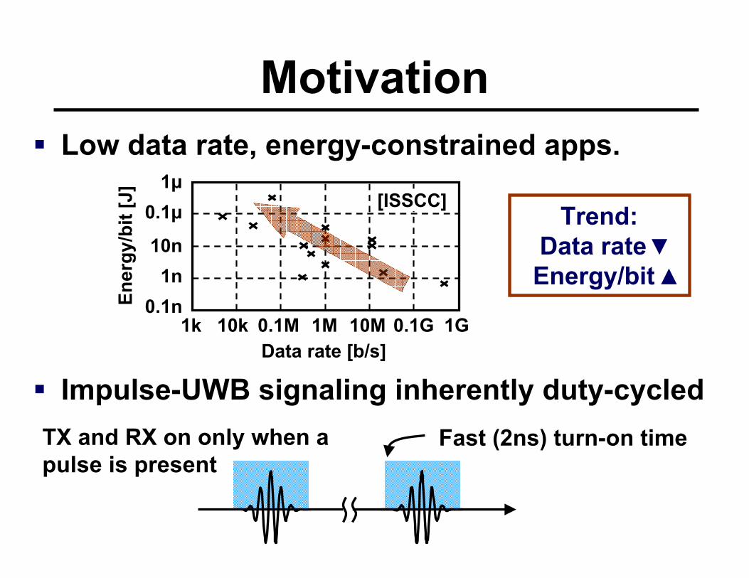
Motivation Low data rate, energy-constrained apps.
Impulse-UWB signaling inherently duty-cycled
1k 10k 0.1M 1M 10M 0.1G 1G0.1n
1n10n
0.1μ1μ
Data rate [b/s]
Ener
gy/b
it [J
]
Trend:Data rateEnergy/bit
Fast (2ns) turn-on timeTX and RX on only when apulse is present
[ISSCC]
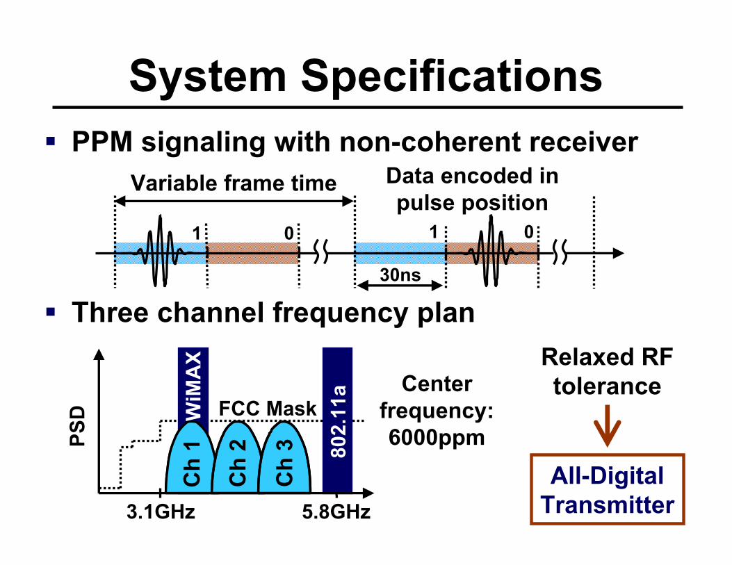
PPM signaling with non-coherent receiver
Three channel frequency plan
System Specifications
Data encoded inpulse position
Variable frame time
30ns
1 0 1 0
All-DigitalTransmitter
Relaxed RFtoleranceCenter
frequency:6000ppm
3.1GHz 5.8GHz
802.
11a
WiM
AX
PSD FCC Mask
Ch
1
Ch
2
Ch
3
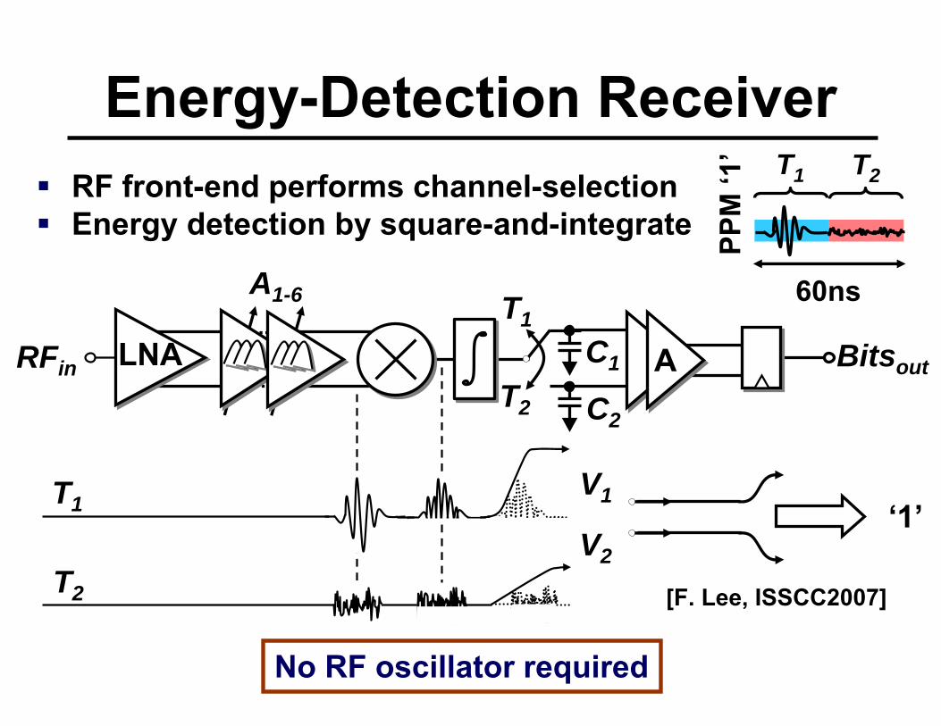
Energy-Detection ReceiverRF front-end performs channel-selectionEnergy detection by square-and-integrate
RFin LNA BitsoutAT1
T2
C1
C2
A1-6
T1 T2
PPM
‘1’
60ns
V1
V2‘1’
T1
T2
No RF oscillator required
[F. Lee, ISSCC2007]
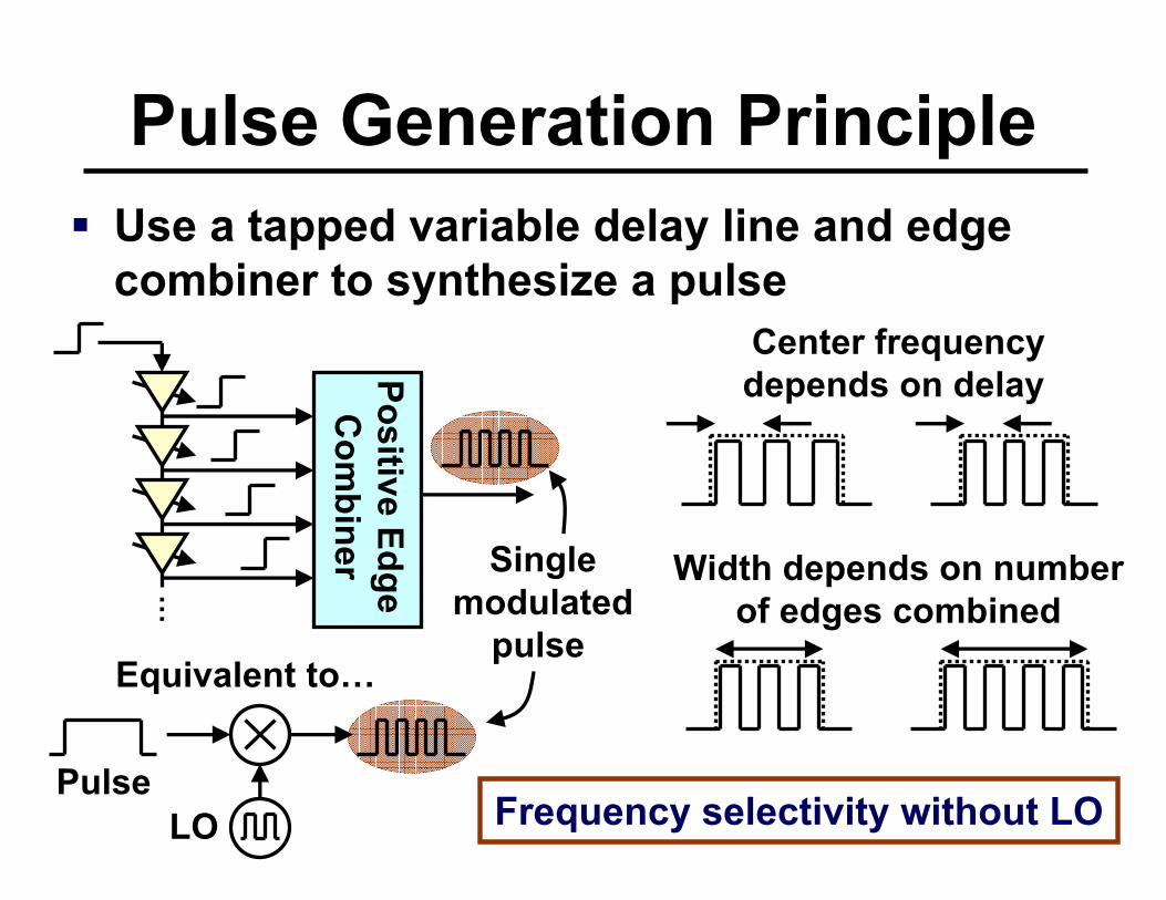
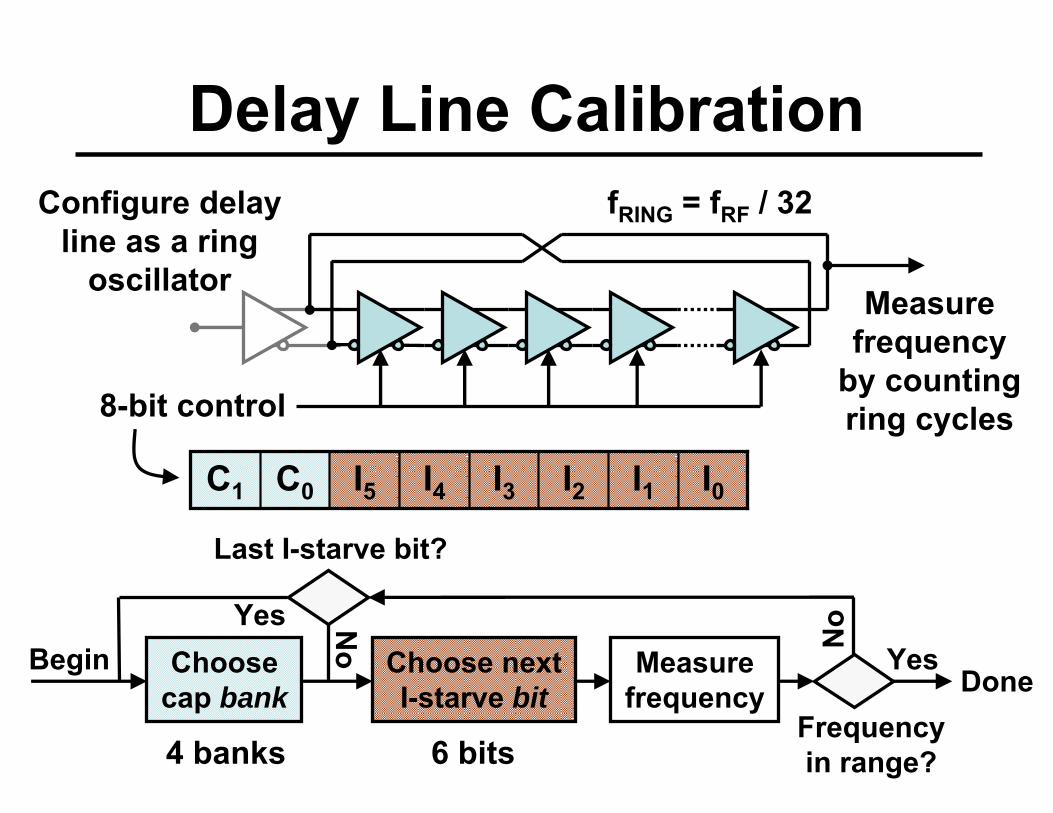
Pulse Generation PrincipleUse a tapped variable delay line and edge combiner to synthesize a pulse
…
Positive EdgeC
ombinerFrequency selectivity without LO
Equivalent to…
Center frequencydepends on delay
Width depends on numberof edges combined
Singlemodulated
pulse
LO Pulse
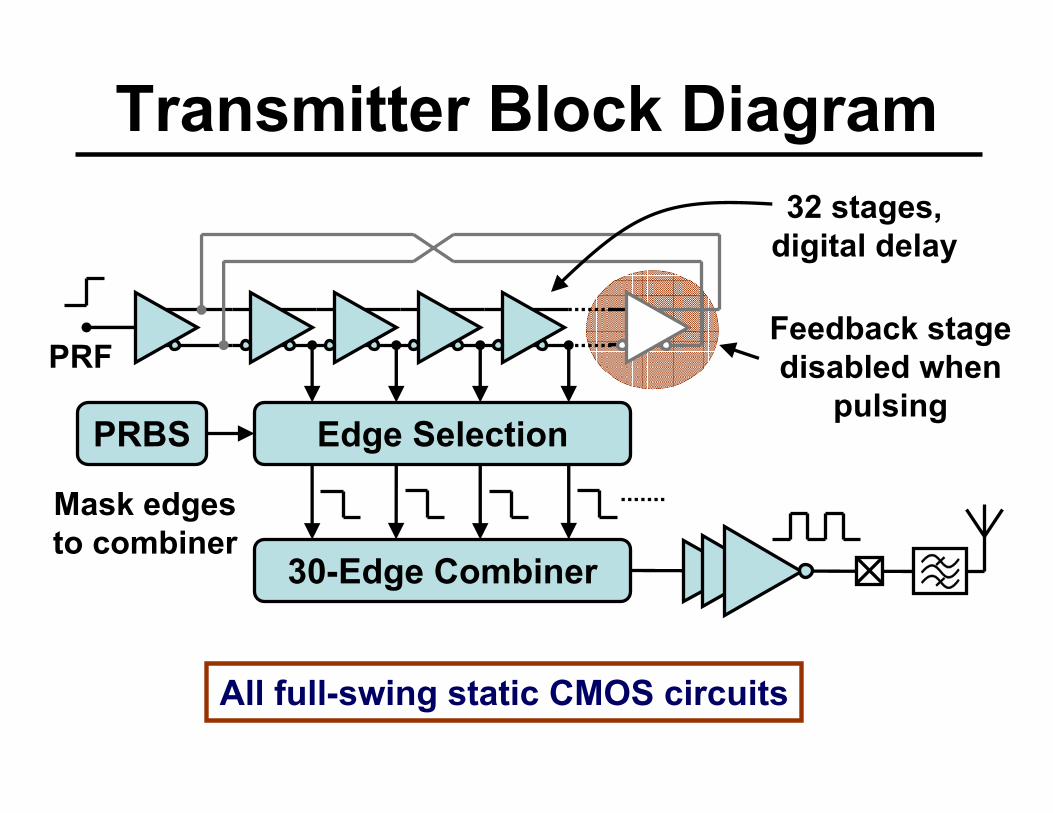
Transmitter Block Diagram
Edge Selection
Feedback stagedisabled when
pulsing
32 stages,digital delay
30-Edge Combiner
Mask edgesto combiner
PRBS
PRF
All full-swing static CMOS circuits

Digital Delay Stage
Full-swingsignals
R1[n]
R2[n]
Only selected edgesare combined
25f 50f
25f 50f
____in[n]
in[n]
in[n+1]______in[n+1]
Overall ±30%variation in delay
6-bitcurrentstarving
8-bit delaycontrol
2-bitcap bank
PRBS
Choosecap bank
Choose nextI-starve bit
Delay Line CalibrationConfigure delay
line as a ringoscillator
Frequencyin range?
YesDone
No
Last I-starve bit?
Yes NoBegin
I0I1I2I3I4I5C0C1
8-bit control
Measurefrequency
4 banks 6 bits
Measurefrequency
by countingring cycles
fRING = fRF / 32
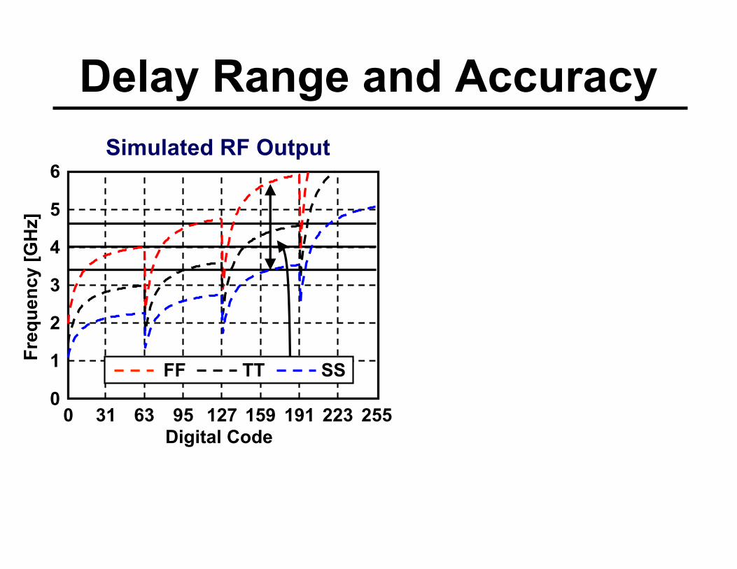
Delay Range and AccuracySimulated RF Output
0 31 63 95 127 159 191 223 2550
1
2
3
4
5
6
Digital Code
Freq
uenc
y [G
Hz]
FF TT SS
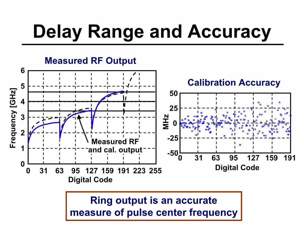
Delay Range and Accuracy
Calibration Accuracy
0 31 63 95 127 159 191-50
-25
0
25
50
Digital CodeM
Hz
Ring output is an accuratemeasure of pulse center frequency
Measured RF Output
0 31 63 95 127 159 191 223 2550
1
2
3
4
5
6
Digital Code
Freq
uenc
y [G
Hz]
Measured RFand cal. output
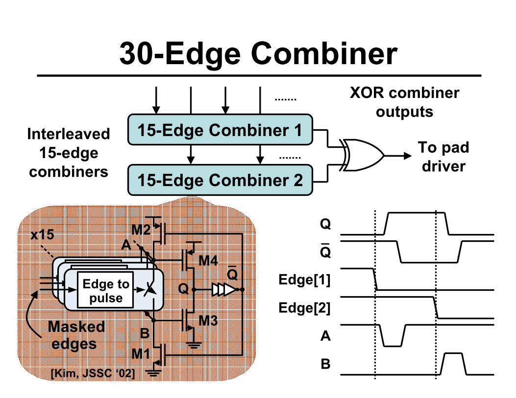
30-Edge Combiner
Interleaved15-edge
combiners
15-Edge Combiner 1
15-Edge Combiner 2
Edge topulse
_Q
A
B
x15
Q
XOR combineroutputs
To paddriver
A
B
_Q
Q
Edge[1]
Maskededges
Edge[2]
[Kim, JSSC ‘02]
M2
M1
M3
M4
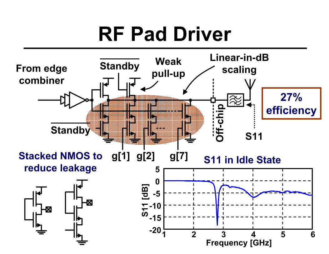
RF Pad Driver
Off-
chip
g[1] g[2] g[7]
_______Standby
_______Standby
From edgecombiner
Linear-in-dBscaling
27%efficiency
Weakpull-up
1 2 3 4 5 6-20-15-10-505
Frequency [GHz]
S11
[dB
]
S11 in Idle StateStacked NMOS toreduce leakage
S11
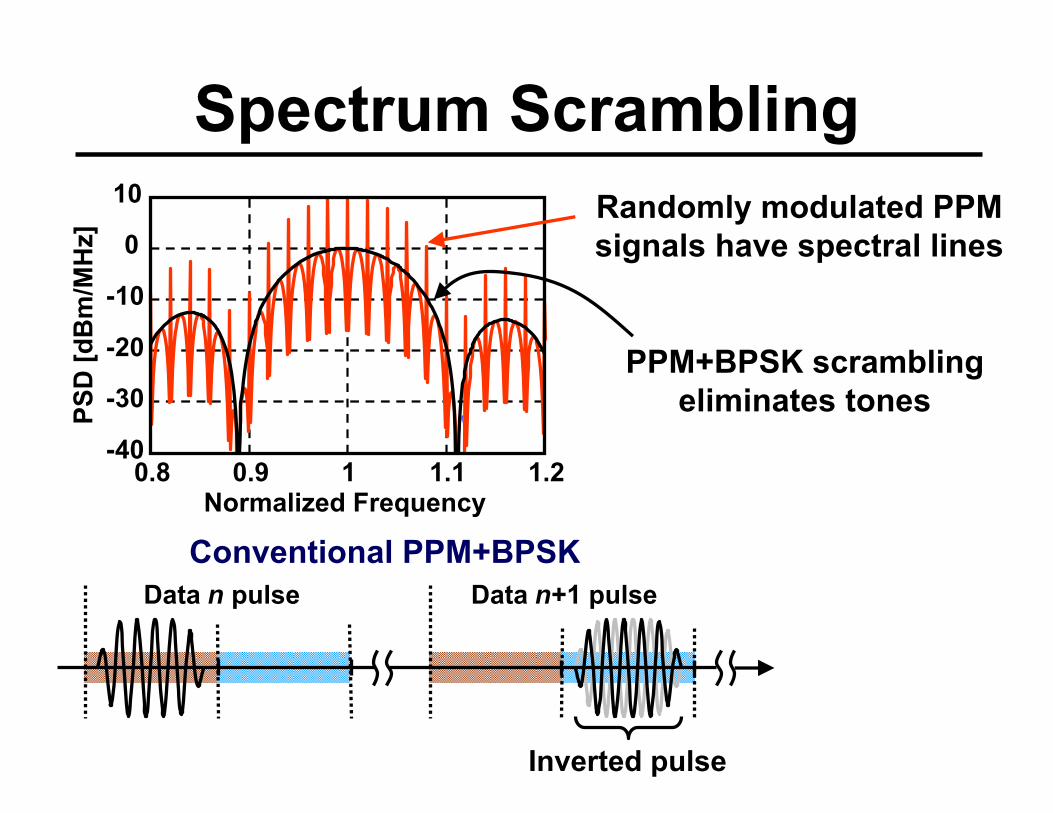
Inverted pulse
Conventional PPM+BPSK
Spectrum ScramblingRandomly modulated PPMsignals have spectral lines
PPM+BPSK scramblingeliminates tones
0.8 0.9 1 1.1 1.2Normalized Frequency
-40
-30
-20
-10
0
10
PSD
[dB
m/M
Hz]
Data n pulse Data n+1 pulse
0.8 0.9 1 1.1 1.2Normalized Frequency
-40
-30
-20
-10
0
10
PSD
[dB
m/M
Hz]
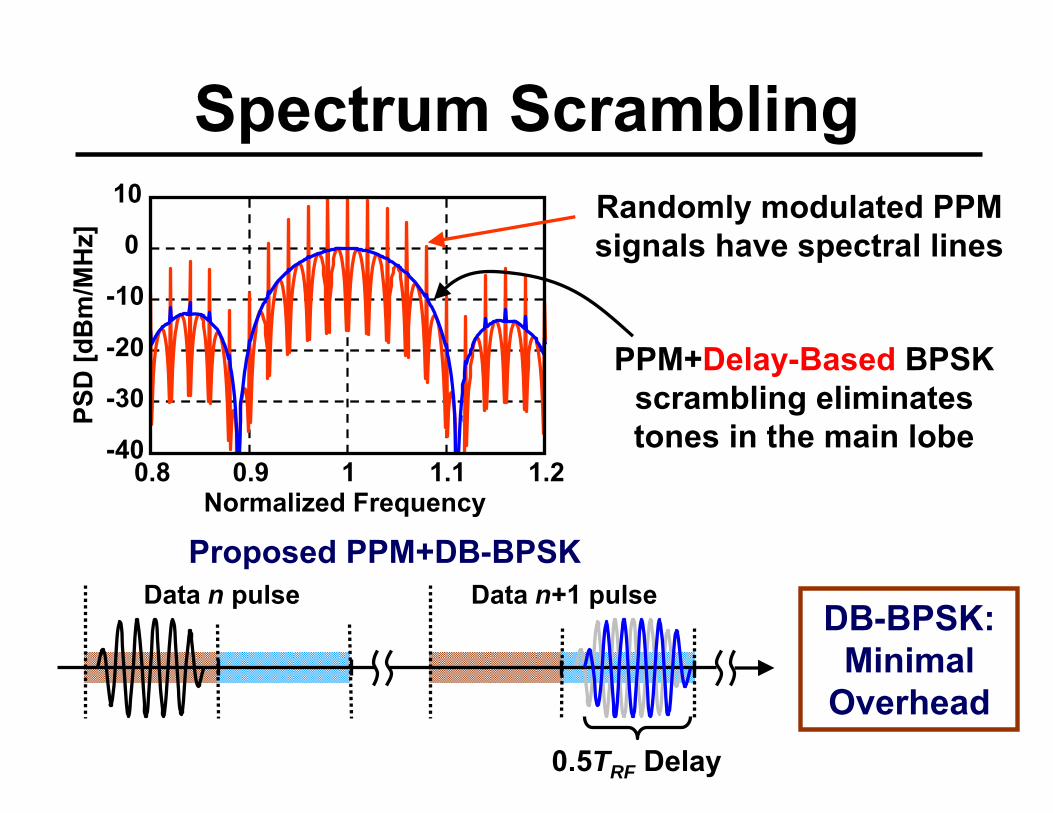
0.5TRF Delay
Spectrum Scrambling
DB-BPSK: Minimal
Overhead
Randomly modulated PPMsignals have spectral lines
PPM+Delay-Based BPSKscrambling eliminatestones in the main lobe
Proposed PPM+DB-BPSKData n pulse Data n+1 pulse
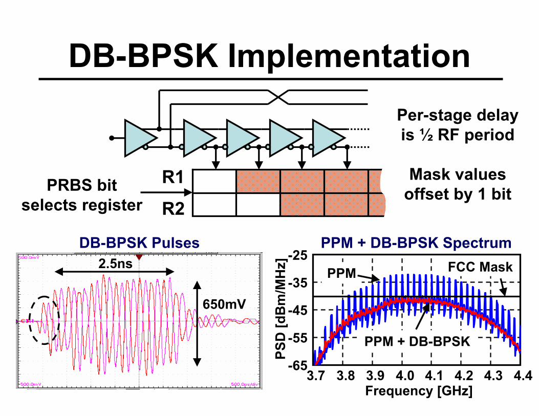
DB-BPSK Implementation
DB-BPSK Pulses PPM + DB-BPSK Spectrum
3.7 3.8 3.9 4.0 4.1 4.2 4.3 4.4-65
-55
-45
-35
-25
Frequency [GHz]
PSD
[dB
m/M
Hz] PPM
PPM + DB-BPSK
R1
R2PRBS bit
selects register
2.5ns
650mV
FCC Mask
Per-stage delayis ½ RF period
Mask valuesoffset by 1 bit
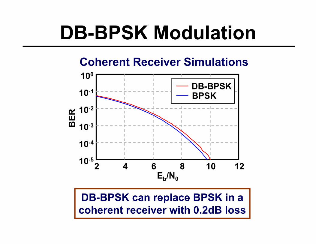
2 4 6 8 10 1210-5
10-4
10-3
10-2
10-1
100
Eb/N0
BER
DB-BPSKBPSK
DB-BPSK Modulation
DB-BPSK can replace BPSK in acoherent receiver with 0.2dB loss
Coherent Receiver Simulations
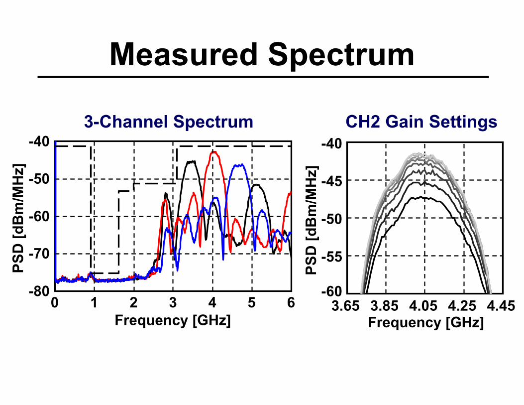
Measured Spectrum
3.65 3.85 4.05 4.25 4.45-60
-55
-50
-45
-40
Frequency [GHz]PS
D [d
Bm
/MH
z]
3-Channel Spectrum CH2 Gain Settings
1 2 3 4 5 6-80
-70
-60
-50
-40
Frequency [GHz]
PSD
[dB
m/M
Hz]
0
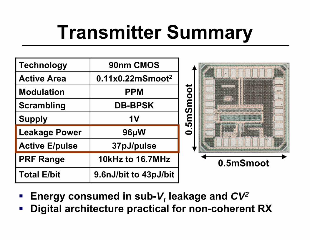
Transmitter Summary
Energy consumed in sub-Vt leakage and CV2
Digital architecture practical for non-coherent RX
10kHz to 16.7MHzPRF Range
9.6nJ/bit to 43pJ/bitTotal E/bit
37pJ/pulseActive E/pulse96μWLeakage Power
1VSupplyDB-BPSKScrambling
PPMModulation0.11x0.22mSmoot2Active Area
90nm CMOSTechnology
0.5mSmoot
0.5m
Smoo
t
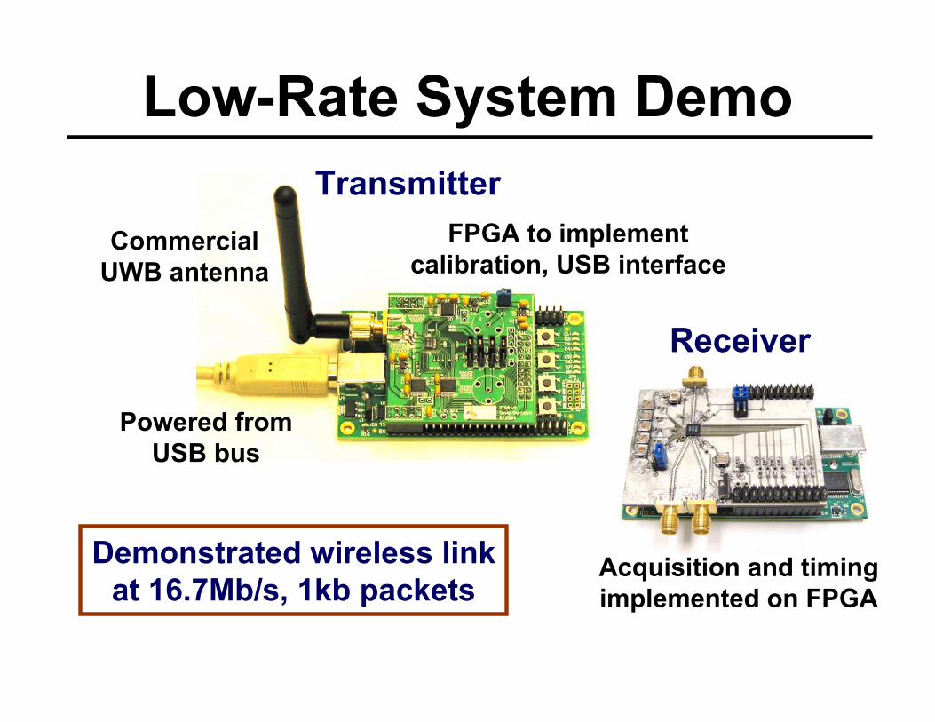
Low-Rate System Demo
Receiver
Transmitter
Powered fromUSB bus
FPGA to implementcalibration, USB interface
CommercialUWB antenna
Demonstrated wireless linkat 16.7Mb/s, 1kb packets
Acquisition and timingimplemented on FPGA
OutlineHigh data rate transmitter– Gaussian pulse shaping
Variable low data rate transmitter– All-digital architecture
Conclusions and future directions
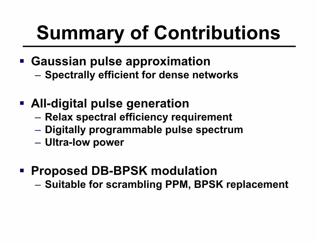
Summary of ContributionsGaussian pulse approximation– Spectrally efficient for dense networks
All-digital pulse generation– Relax spectral efficiency requirement– Digitally programmable pulse spectrum– Ultra-low power
Proposed DB-BPSK modulation– Suitable for scrambling PPM, BPSK replacement
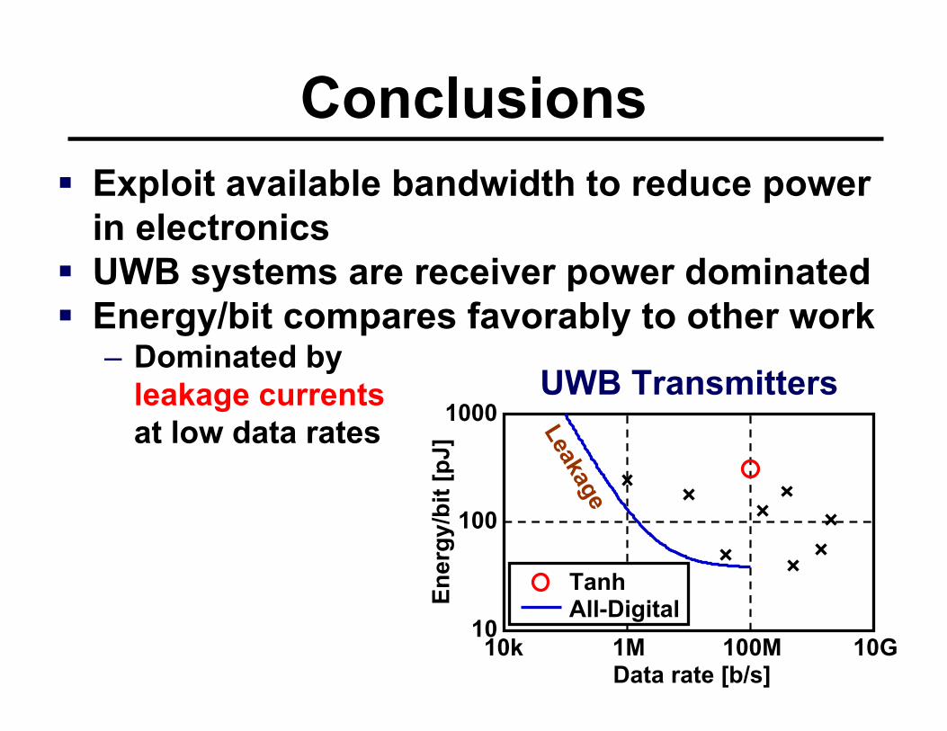
ConclusionsExploit available bandwidth to reduce power in electronicsUWB systems are receiver power dominatedEnergy/bit compares favorably to other work– Dominated by
leakage currentsat low data rates
UWB Transmitters
10k 1M 100M 10G10
100
1000En
ergy
/bit
[pJ]
Data rate [b/s]
Leakage
TanhAll-Digital
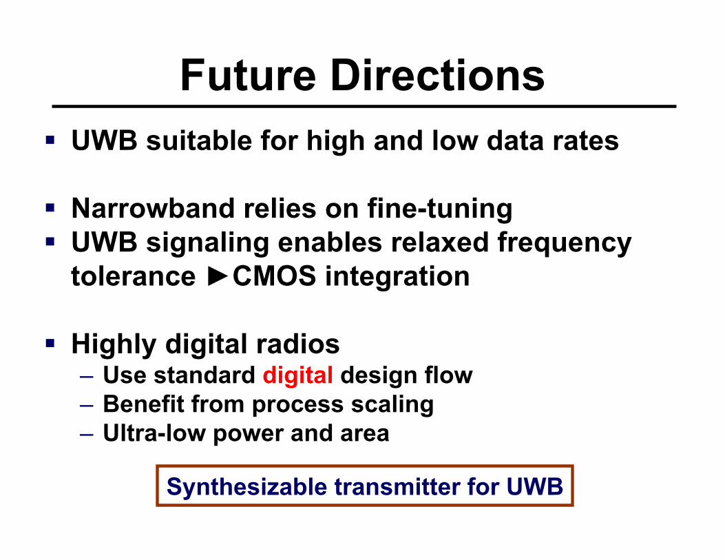
Future DirectionsUWB suitable for high and low data rates
Narrowband relies on fine-tuningUWB signaling enables relaxed frequency tolerance ►CMOS integration
Highly digital radios– Use standard digital design flow– Benefit from process scaling– Ultra-low power and area
Synthesizable transmitter for UWB
AcknowledgementsAnantha ChandrakasanJoel Dawson and Charlie SodiniMargaret FlahertyFriends@MIT and familyMARCO/DARPA Focus Center for Circuits and Systems Solutions (C2S2), National Science Foundation (NSF), HP/MIT AllianceSTMicroelectronics for chip fabrication
Thank YOU for your attention