Embed Size (px)
Citation preview
ISSN: 2319-8753
International Journal of Innovative Research in Science,
Engineering and Technology
(An ISO 3297: 2007 Certified Organization)
Vol. 3, Issue 3, March 2014
Copyright to IJIRSET www.ijirset.com 10445
Study and Implementation of Gain Boost Class-C
Inverter in CMOS 50nm Technology Atulkumar Sojitra
1, Arun Nandurbarkar
2
P.G student, Department of Electronics & Communication, L.D.College of Engineering, Ahmedabad, Gujarat, India,
Associate Professor, Department of Electronics & Communication, L.D.College of Engineering, Ahmedabad, Gujarat,India2
Abstract:This paper describes the Gain boost class–C inverter circuit, which is used in place of OTA (Operational Trans-
conductance Amplifier) block in ∑Δ modulator .The gain boost class-C inverter behaves as a low voltage, subthreshold
amplifier and boosts its DC gain for the high precision requirement. First a traditional cascade class-C inverter is presented,
another inverter circuit present in this paper is “Gain boost class-C inverter”. It is implemented in 50nm CMOS technology and
simulation is done using the LTSpice simulation tool.
Keywords: CMOS, cascode inverter, LT-Spice, gain boost class-C inverter.
I. INTRODUCTION
The continuing feature size scaling in CMOS technology has enabled the digital system to decrease power consumption and
lower costs while also increasing reliability. The supply voltages must be scaled along with transistor dimension to maintain the
device’s reliability. However, the threshold voltage is not scaled as aggressively as the supply voltage to avoid leakage current
in transistors. Therefore, the design of low-voltage analog circuits in the scaled CMOS technology poses significant challenges.
Especially, the design of an operational transconductance amplifier (OTA), a key analog building block, has been the main
bottleneck in low-voltage analog circuits. Low voltage OTAs have been explored [1]–[2], but the supply voltages of the OTAs
are restricted and have reached the limits of further scaling, because they are strictly limited by the input common-mode
voltage.
A number of design techniques have been investigated to overcome these challenge. Considering the OTA itself, a body-driven
OTA and digitally assisted OTAs, have been reported. To remove the need for OTAs, comparator-based [3], time-based [4], and
charge-domain [5] circuits have been proposed. A comparator-based circuit is proposed to replace an OTA by a comparator and
current sources [3] that remove feedback and stability concerns, but a comparator also has difficulties with low supply voltages.
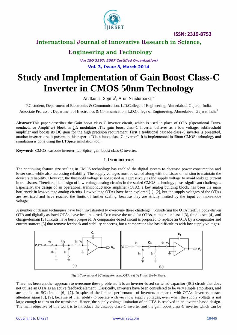
Fig. 1 Conventional SC integrator using OTA. (a) Φ1 Phase. (b) Φ2 Phase.
There has been another approach to overcome these problems. It is an inverter-based switched-capacitor (SC) circuit that does
not utilize an OTA as an active feedback element. Classically, inverters have been considered to be very simple amplifiers, and
are applied to SC circuits [6], [7]. In spite of the limited performance of inverters compared with OTAs, inverters attract
attention again [8], [9], because of their ability to operate with very low supply voltages, even when the supply voltage is not
large enough to turn on the transistors. Hence, the supply voltage limitation of an OTA is resolved in an inverter-based design.
The main objective of this work is to introduce the cascade class-C inverter and the gain boost class-C inverter which can be
ISSN: 2319-8753
International Journal of Innovative Research in Science,
Engineering and Technology
(An ISO 3297: 2007 Certified Organization)
Vol. 3, Issue 3, March 2014
Copyright to IJIRSET www.ijirset.com 10446
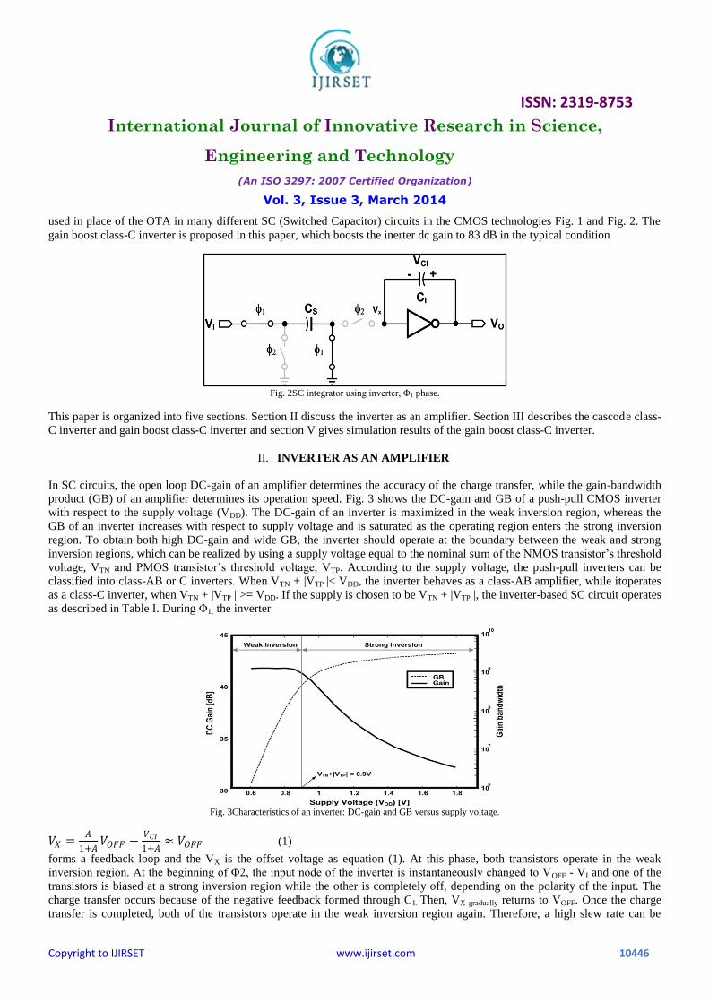
used in place of the OTA in many different SC (Switched Capacitor) circuits in the CMOS technologies Fig. 1 and Fig. 2. The
gain boost class-C inverter is proposed in this paper, which boosts the inerter dc gain to 83 dB in the typical condition
Fig. 2SC integrator using inverter, Φ1 phase.
This paper is organized into five sections. Section II discuss the inverter as an amplifier. Section III describes the cascode class-
C inverter and gain boost class-C inverter and section V gives simulation results of the gain boost class-C inverter.
II. INVERTER AS AN AMPLIFIER
In SC circuits, the open loop DC-gain of an amplifier determines the accuracy of the charge transfer, while the gain-bandwidth
product (GB) of an amplifier determines its operation speed. Fig. 3 shows the DC-gain and GB of a push-pull CMOS inverter
with respect to the supply voltage (VDD). The DC-gain of an inverter is maximized in the weak inversion region, whereas the
GB of an inverter increases with respect to supply voltage and is saturated as the operating region enters the strong inversion
region. To obtain both high DC-gain and wide GB, the inverter should operate at the boundary between the weak and strong
inversion regions, which can be realized by using a supply voltage equal to the nominal sum of the NMOS transistor’s threshold
voltage, VTN and PMOS transistor’s threshold voltage, VTP. According to the supply voltage, the push-pull inverters can be
classified into class-AB or C inverters. When VTN + |VTP |< VDD, the inverter behaves as a class-AB amplifier, while itoperates
as a class-C inverter, when VTN + |VTP | >= VDD. If the supply is chosen to be VTN + |VTP |, the inverter-based SC circuit operates
as described in Table I. During Φ1, the inverter
Fig. 3Characteristics of an inverter: DC-gain and GB versus supply voltage.
𝑉𝑋 =𝐴
1+𝐴𝑉𝑂𝐹𝐹 −
𝑉𝐶𝐼
1+𝐴≈ 𝑉𝑂𝐹𝐹 (1)
forms a feedback loop and the VX is the offset voltage as equation (1). At this phase, both transistors operate in the weak
inversion region. At the beginning of Φ2, the input node of the inverter is instantaneously changed to VOFF - VI and one of the
transistors is biased at a strong inversion region while the other is completely off, depending on the polarity of the input. The
charge transfer occurs because of the negative feedback formed through CI. Then, VX gradually returns to VOFF. Once the charge
transfer is completed, both of the transistors operate in the weak inversion region again. Therefore, a high slew rate can be
ISSN: 2319-8753
International Journal of Innovative Research in Science,
Engineering and Technology
(An ISO 3297: 2007 Certified Organization)
Vol. 3, Issue 3, March 2014
Copyright to IJIRSET www.ijirset.com 10447
obtained with minimum static current because one necessary transistor is operating in the strong inversion region providing high
slew rate during transition, and then both transistors operate in the weak inversion region during the steady state providing
highDC-gain. Fig. 4 shows the simulated step response of an inverter-based SC integrator when VDD = |VTP |+ VTN. The large
signal-dependent current flows only during the transition while the static current is kept very low. When a class-C inverter is
used foran amplifier, the settling time can be reduced by about 75% without increasing the static current, because it has a very
low short circuit current. Table I
Operation of class-c inverter at different clock phase
Fig. 4Simulated step response: output voltage and driven current at VDD.
III. CASCODE AND GAIN BOOST CLASS-C INVERTER
As we known, class-C inverter acts as a subthreshold amplifier [10], which is the most important module in the inverter-based
design. In this section, the design and application of a gain-boost class-C inverter will be introduced in detail.
ISSN: 2319-8753
International Journal of Innovative Research in Science,
Engineering and Technology
(An ISO 3297: 2007 Certified Organization)
Vol. 3, Issue 3, March 2014
Copyright to IJIRSET www.ijirset.com 10448
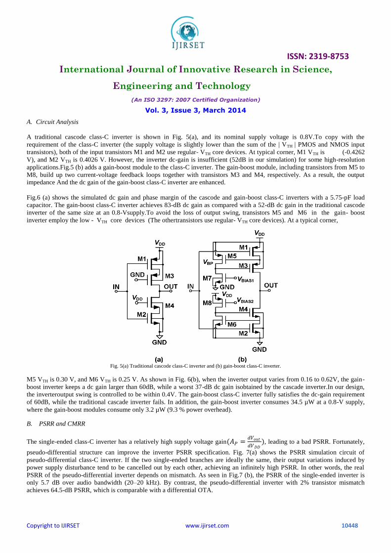
A. Circuit Analysis
A traditional cascode class-C inverter is shown in Fig. 5(a), and its nominal supply voltage is 0.8V.To copy with the
requirement of the class-C inverter (the supply voltage is slightly lower than the sum of the | VTH | PMOS and NMOS input
transistors), both of the input transistors M1 and M2 use regular- VTH core devices. At typical corner, M1 VTH is (-0.4262
V), and M2 VTH is 0.4026 V. However, the inverter dc-gain is insufficient (52dB in our simulation) for some high-resolution
applications.Fig.5 (b) adds a gain-boost module to the class-C inverter. The gain-boost module, including transistors from M5 to
M8, build up two current-voltage feedback loops together with transistors M3 and M4, respectively. As a result, the output
impedance And the dc gain of the gain-boost class-C inverter are enhanced.
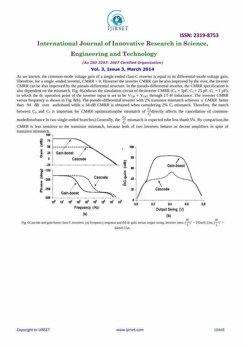
Fig.6 (a) shows the simulated dc gain and phase margin of the cascode and gain-boost class-C inverters with a 5.75-pF load
capacitor. The gain-boost class-C inverter achieves 83-dB dc gain as compared with a 52-dB dc gain in the traditional cascode
inverter of the same size at an 0.8-Vsupply.To avoid the loss of output swing, transistors M5 and M6 in the gain- boost
inverter employ the low - VTH core devices (The othertransistors use regular- VTH core devices). At a typical corner,
Fig. 5(a) Traditional cascode class-C inverter and (b) gain-boost class-C inverter.
M5 VTH is 0.30 V, and M6 VTH is 0.25 V. As shown in Fig. 6(b), when the inverter output varies from 0.16 to 0.62V, the gain-
boost inverter keeps a dc gain larger than 60dB, while a worst 37-dB dc gain isobtained by the cascade inverter.In our design,
the inverteroutput swing is controlled to be within 0.4V. The gain-boost class-C inverter fully satisfies the dc-gain requirement
of 60dB, while the traditional cascade inverter fails. In addition, the gain-boost inverter consumes 34.5 µW at a 0.8-V supply,
where the gain-boost modules consume only 3.2 µW (9.3 % power overhead).
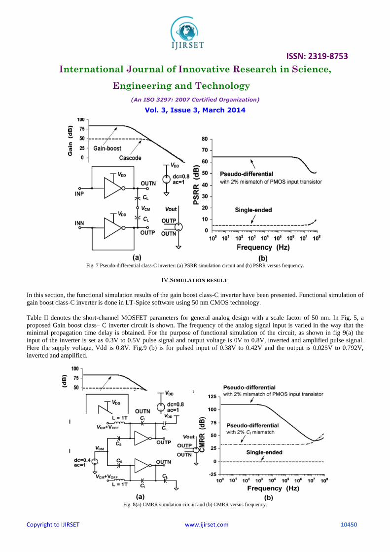
B. PSRR and CMRR
The single-ended class-C inverter has a relatively high supply voltage gain(𝐴𝑃 =𝑑𝑉𝑜𝑢𝑡
𝑑𝑉𝐷𝐷), leading to a bad PSRR. Fortunately,
pseudo-differential structure can improve the inverter PSRR specification. Fig. 7(a) shows the PSRR simulation circuit of
pseudo-differential class-C inverter. If the two single-ended branches are ideally the same, their output variations induced by
power supply disturbance tend to be cancelled out by each other, achieving an infinitely high PSRR. In other words, the real
PSRR of the pseudo-differential inverter depends on mismatch. As seen in Fig.7 (b), the PSRR of the single-ended inverter is
only 5.7 dB over audio bandwidth (20–20 kHz). By contrast, the pseudo-differential inverter with 2% transistor mismatch
achieves 64.5-dB PSRR, which is comparable with a differential OTA.
ISSN: 2319-8753
International Journal of Innovative Research in Science,
Engineering and Technology
(An ISO 3297: 2007 Certified Organization)
Vol. 3, Issue 3, March 2014
Copyright to IJIRSET www.ijirset.com 10449
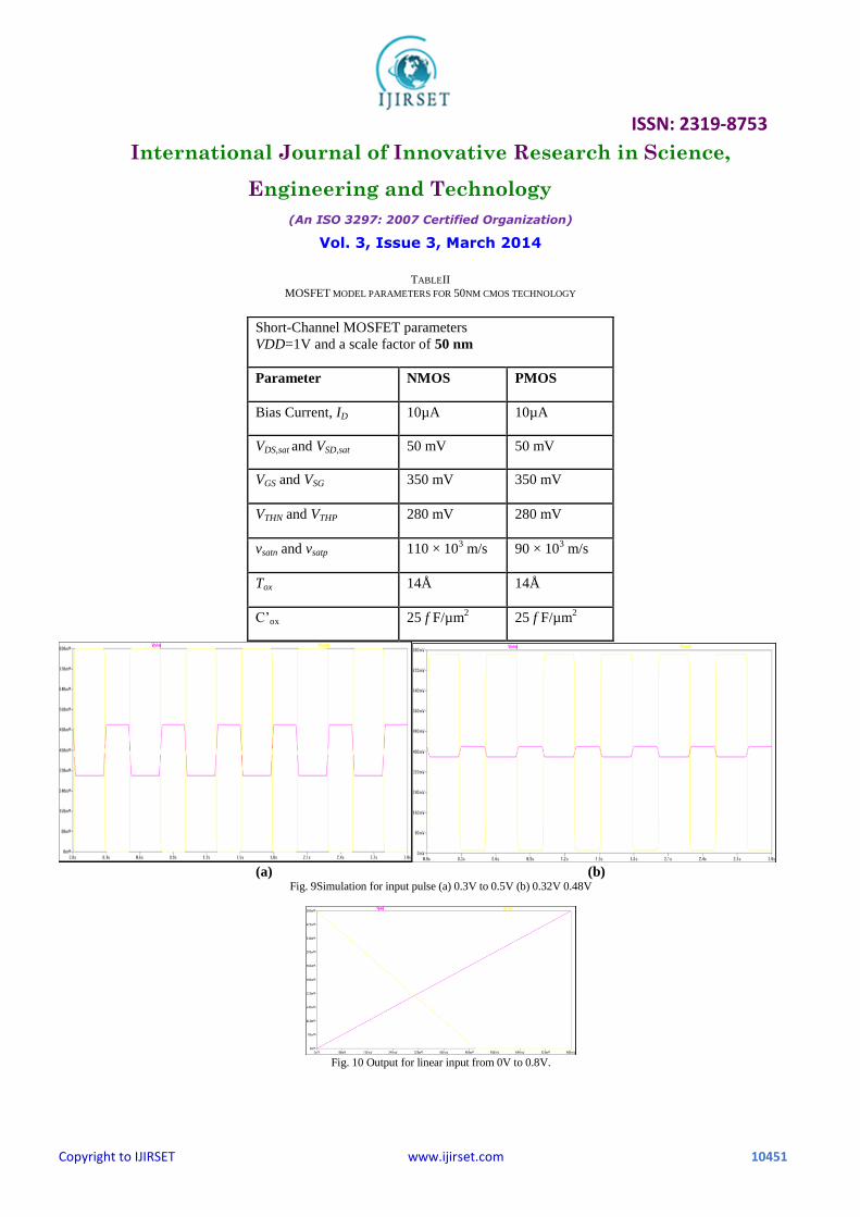
As we known, the common-mode voltage gain of a single-ended class-C inverter is equal to its differential-mode voltage gain.
Therefore, for a single -ended inverter, CMRR = 0. However the inverter CMRR can be also improved by the ever, the inverter
CMRR can be also improved by the pseudo-differential structure. In the pseudo-differential inverter, the CMRR specification is
also dependent on the mismatch. Fig. 8(a)shows the simulation circuit of theinverter CMRR (CS = 5pF, CI = 25 pF, CL = 1 pF),
in which the dc operation point of the inverter input is set to be VCM + VOFF through 1T-H inductance. The inverter CMRR
versus frequency is shown in Fig. 8(b). The pseudo-differential inverter with 2% transistor mismatch achieves a CMRR better
than 94 dB over audioband while a 34-dB CMRR is obtained when considering 2% CI mismatch. Therefore, the match
between CS and CI is important for CMRR optimization(the mismatch of 𝐶𝑆
𝐶𝐼directly affects the cancellation of common-
modedisturbance in two single-ended branches).Generally, the 𝐶𝑆
𝐶𝐼 mismatch is expected tobe less than0.5%. By comparison,the
CMRR is less sensitive to the transistor mismatch, because both of two inverters behave as decent amplifiers in spite of
transistor mismatch.
Fig. 6Cascode and gain-boost class-C inverters: (a) Frequency response and (b) dc gain versus output swing. Inverter sizes: (𝑊
𝐿) 2 = 192m/0.15m, (
𝑊
𝐿) 2 =
64m/0.15m.
ISSN: 2319-8753
International Journal of Innovative Research in Science,
Engineering and Technology
(An ISO 3297: 2007 Certified Organization)
Vol. 3, Issue 3, March 2014
Copyright to IJIRSET www.ijirset.com 10450
Fig. 7 Pseudo-differential class-C inverter: (a) PSRR simulation circuit and (b) PSRR versus frequency.
IV.SIMULATION RESULT
In this section, the functional simulation results of the gain boost class-C inverter have been presented. Functional simulation of
gain boost class-C inverter is done in LT-Spice software using 50 nm CMOS technology.
Table II denotes the short-channel MOSFET parameters for general analog design with a scale factor of 50 nm. In Fig. 5, a
proposed Gain boost class– C inverter circuit is shown. The frequency of the analog signal input is varied in the way that the
minimal propagation time delay is obtained. For the purpose of functional simulation of the circuit, as shown in fig 9(a) the
input of the inverter is set as 0.3V to 0.5V pulse signal and output voltage is 0V to 0.8V, inverted and amplified pulse signal.
Here the supply voltage, Vdd is 0.8V. Fig.9 (b) is for pulsed input of 0.38V to 0.42V and the output is 0.025V to 0.792V,
inverted and amplified.
Fig. 8(a) CMRR simulation circuit and (b) CMRR versus frequency.
ISSN: 2319-8753
International Journal of Innovative Research in Science,
Engineering and Technology
(An ISO 3297: 2007 Certified Organization)
Vol. 3, Issue 3, March 2014
Copyright to IJIRSET www.ijirset.com 10451
TABLEII
MOSFET MODEL PARAMETERS FOR 50NM CMOS TECHNOLOGY
(a) (b)
Fig. 9Simulation for input pulse (a) 0.3V to 0.5V (b) 0.32V 0.48V
Fig. 10 Output for linear input from 0V to 0.8V.
Short-Channel MOSFET parameters
VDD=1V and a scale factor of 50 nm
Parameter NMOS PMOS
Bias Current, ID 10µA 10µA
VDS,sat and VSD,sat 50 mV 50 mV
VGS and VSG 350 mV 350 mV
VTHN and VTHP 280 mV 280 mV
vsatn and vsatp 110 × 103 m/s 90 × 10
3 m/s
Tox 14Å 14Å
C’ox 25 f F/µm2 25 f F/µm
2
ISSN: 2319-8753
International Journal of Innovative Research in Science,
Engineering and Technology
(An ISO 3297: 2007 Certified Organization)
Vol. 3, Issue 3, March 2014
Copyright to IJIRSET www.ijirset.com 10452
V.CONCLUSION
IN THIS PAPER, A GAIN BOOST CLASS-C INVERTER CIRCUIT IS PROPOSED. OTA HAS A PROBLEM WITH THE REQUIREMENT OF
HIGHER POWER SUPPLY AND CASCODE CLASS-C INVERTER HAS LOWER DC GAIN WHICH IS LESS SUITABLE FOR DIFFERENT SIGMA
DELTA MODULATOR. GAIN BOOST CLASS-C INERTER IS PRESENTED USING 50NM CMOS TECHNOLOGY. THIS ARCHITECTURE
ACHIEVES DC GAIN OF 83- DB. AS A FUTURE WORK, WE CAN DESIGN LOW POWER LOW VOLTAGE INVERTER BASED ∑∆
MODULATOR USING THIS INVERTER DESIGN.
REFERENCES
[1]. L. Yao, M. S. J. Steyaert, and W. Sansen, “A 1-V 140-µW88-dB audio sigma-delta modulator in 90-nm CMOS,” in IEEE J. Solid-State Circuits, vol. 39,
no. 11, pp. 1809–1818, Nov. 2004.
[2]. J. Goes, B. Vaz, R. Monteiro, and N. Paulino, “A 0.9-V sigma delta modulator with 80 dB SNDR and 83 dB DR using a single-phase technique,” IEEE Int. Solid-State Circuits Conf. Dig. Tech. Papers, Feb. 2006, pp. 74–75.
[3]. J. K. Fiorenza, T. Sepke, P. Holloway, C. G. Sodini, and H.-S. Lee, “Comparator-based switched-capacitor circuits dor scaled CMOS technologie,”IEEE
J. Solid-State Circuits, vol. 41, no. 12, pp. 2658–2668, Dec. 2006 [4]. H. Yang and R. Sarpeshkar, “A time-based energy-efficient analog-to-digital converter,” inIEEE J. Solid-State Circuits, vol. 40, no. 8, pp. 1590–1601,
Aug. 2005.
[5]. S. Paul, H.-S. Lee, J. Goodrich, T. Alailima, and D. Santiago, “A Nyquist-rate pipelined oversampling A/D converter,” inIEEE J. Solid-State Circuits, vol. 34, no. 12, pp. 1777–1787, Dec. 1999.
[6]. B. J. Hosticka, “Dynamic CMOS amplifiers,” inIEEE J. Solid-State Circuits, vol. 14, pp. 1111–1114, Dec. 1979.
[7]. F. Krummenacher, “Micropower switched capacitor biquadratic cell,” inIEEE J. Solid-State Circuits, vol. 17, pp. 507–512, June 1982. [8]. B. Nauta, “A CMOS transconductance-C filter technique for very high frequencies,” inIEEE J. Solid-State Circuits, vol. 27, pp. 142–153, Feb. 1992.
[9]. R. H. M. van Veldhoven, R. Rutten, and L. J. Breems, “An inverter based hybrid sigma delta modulator,” in IEEE Int. Solid-State Circuits Conf. Dig.
Tech. Papers, Feb. 2008, pp. 492–493. [10]. Hao Luo,Yan Han, Ray C.C. Cheung, “A 0.8-V 230-µW DR Inverter –Based Sigma Delta Modulator for Audio Applications,” inIEEE J. Solid-State
Circuits, vol. 48, pp. 2430–2441, Oct. 2013.
[11]. R. J. Baker, H. W. Li and D.E Boyce, CMOS Circuit Design, Layout And Simulation, New York, IEEE Press, 2008. [12]. Phillip E. Allen and Douglas R. Holberg, CMOS Analog Circuit Design, Oxford University Press, Inc. 2002.
[13]. Sung-mo Kang, Yusuf Leblebici, “CMOS Digital Integrated Circuits: Analysis and Design”, third edition, Tata McGraw-Hill edition 2003.