Embed Size (px)
DESCRIPTION
An Investigation of Crosstalk on the Rapid Transfer BPM Analog Transition Module PC Board. August 23, 2006 David Peterson Antiproton Source Department Fermi National Accelerator Lab. Acknowledgements. Thanks to : Carl Seifrid John Van Bogaert Bob Dysert Peter Prieto Bob Webber - PowerPoint PPT Presentation
Citation preview

An Investigation of Crosstalk on the
Rapid Transfer BPM Analog Transition Module
PC Board
August 23, 2006David Peterson
Antiproton Source DepartmentFermi National Accelerator Lab

Acknowledgements
Thanks to :Carl Seifrid
John Van Bogaert
Bob Dysert
Peter Prieto
Bob Webber
Nathan Eddy
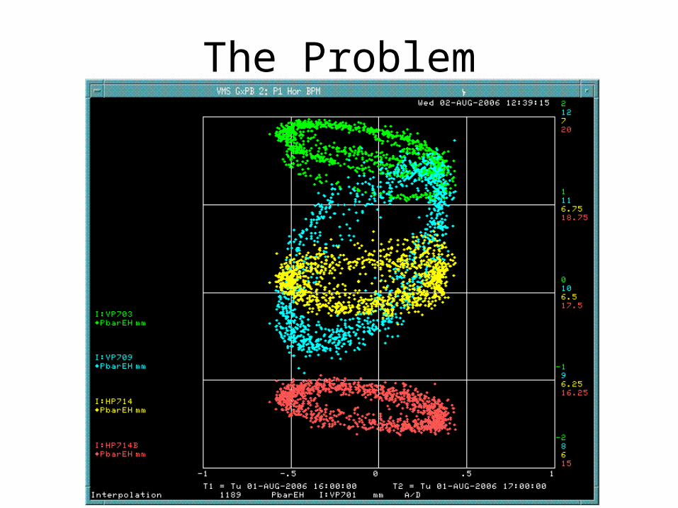
The Problem

Some Clues
Beam signals after the Analog Transition card (53 MHz bandpass filtering) had
1. Strong 53 MHz
2. -40 dB 106 MHz
3. Weak 159
4. Some 212
5. Even more 265 and so on…
6. Strong 424 MHz!

More Clues
• Splitting one beam signal four ways into BPM also produced ellipses.
• Splitting one Arbitrary Waveform Generator signal four ways into BPM did not produce ellipses.
• Adding low pass filters to beam signals eliminated ellipses.

Frequency Response Measurement
Green = A1 In to A1 OutViolet = A1 In to B1 Out
Transition Board S21 showing desired channel and isolation to adjacent channel.

More Tests
• The EchoTek board is sensitive to 424 MHzADC Counts:
Noise (No input) = 5-653.1MHz = 1,800318.6MHz = 50371MHz = 12424.8MHz = 260477.9MHz = 10
• The Transition PC card exhibited coupling from one input channel to all others.
• Coupling was not affected by DC power or relay settings.

Where? How?
Needless to say, this was quite mysterious.
Since a bare prototype board was available it was decided to start with the SMB connectors and add components until the crosstalk was observed.
It didn’t take long.

Only SMB Connectorson the board
Did I miss something?
Just to make sure RF fundamentals haven’t changed, I put two SMB connectors on a simple test board with microstrip lines and the same spacing as on the Transition card.
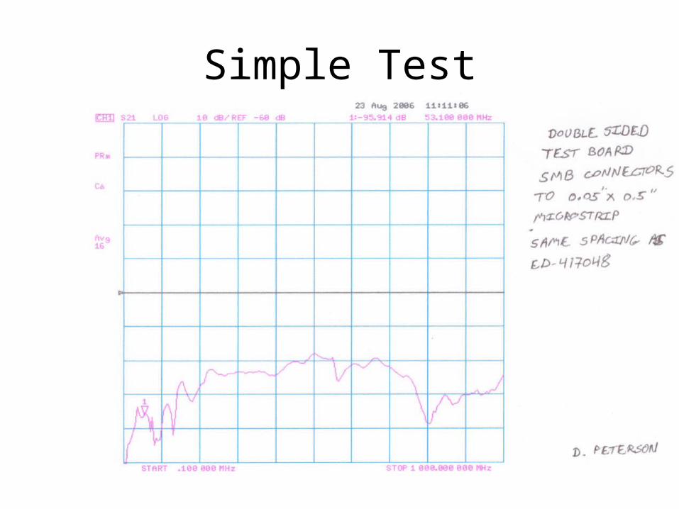
Simple Test

Why the Difference?The simple test board only has signal and ground planes.
The Transition Card has 6 layers:1) Top (signals and some grounding)2) -5 volts (full size of board)3) +5 volts (full size of board)4) Signals5) Ground6) Bottom (some signals, mostly ground)
The ground pads of Top and Bottom all connect to the Ground layer.
Unfortunately, the -5 volt layer is not bypassed to ground very near the input connectors.
This creates a nice broadside coupled line structure since the -5 volt layer is free to "wave in the breeze".

Board Layout
Area of Interest

Board Layers
-5 volt layer
SMB center pinClosest Connection

Recommendations
• Although it is common practice to use power planes as isolation layers, careful attention must be paid to the signal frequencies and return paths.
• A generous number of appropriately placed bypass capacitors might help.
• Better yet, if the design needs a ground plane, use a real ground plane.

Useful Reading
• Thomas P. Van Doren, Grounding & Shielding of Electronic Systems, short course notes (although
you have to take the course to get the notes or talk to me) http://www.emclab.umr.edu/studfac/vandoren.html
• Paul Horowitz and Winfield Hill, The Art of Electronics, 2nd Edition, Cambridge University Press, Chapters 7 & 12.
• Tips for Electronic Printed Circuit Board Design http://www.radioing.com/eengineer/pcb-tips.html