Embed Size (px)
Citation preview
An Embedded DRAM Architecture forLarge-Scale Spatial-Lattice Computations
Norman Margolus!
MIT AI Laboratory545 Technology SquareCambridge MA 02139
ABSTRACTSpatial-lattice computations with finite-range interactionsare an important class of easily parallelized computations.This class includes many simple and direct algorithms forphysical simulation, virtual-reality simulation, agent-basedmodeling, logic simulation, 2D and 3D image processing andrendering, and other volumetric data processing tasks. Therange of applicability of such algorithms is completely de-pendant upon the lattice-sizes and processing speeds thatare computationally feasible. Using embedded DRAM anda new technique for organizing SIMD memory and commu-nications we can e!ciently utilize 1Tbit/sec of sustainedmemory bandwidth in each chip in an indefinitely scalablearray of chips. This allows a 10,000-fold speedup per mem-ory chip for these algorithms compared to the CAM-8 lat-tice gas computer, and is about one million times faster permemory chip for these calculations than a CM-2.
Categories and Subject DescriptorsC.1.2 [Processor Architectures]: Multiprocessors—ar-ray and vector processors, SIMD ; C.1.4 [Processor Ar-chitectures]: Parallel Architectures—distributed architec-tures; C.3 [Computer Systems Organization]: Special-Purpose and Application-Based Systems
KeywordsVirtual Processor, PIM, lattice gas, cellular automata
1. INTRODUCTIONBeginning in 1986, a new class of physical simulation meth-ods were developed based on discrete particles which hoparound and collide on a spatial lattice[11, 20]. These meth-ods provide a simplified molecular dynamics that makes
!Permanent address: Boston University Center for Compu-tational Science, 3 Cummington Street, Boston 02215
direct large-scale simulation of complex fluids and materi-als computationally feasible[2]. Stimulated by the promiseof these new and “embarassingly parallel” lattice gas tech-niques, special purpose SIMD machines were developed thatwere optimized for these kinds of calculations, including theCAM-8 machine, completed in 1992[17]. Although CAM-8’smesh architecture is indefinitely scalable, only small-scaleprototypes were actually built. With an aggregate memorybandwidth a factor of 100 less than a contemporary CM-2and just 8 lookup-table processors, CAM-8 prototypes ranlattice-gas simulations at about the same speed as the CM-2[7, 17]. This demonstrated the usefulness of optimizing aSIMD architecture for discrete spatial lattice simulations.
With its simple high-level lattice-gas programming model,CAM-8 was used to develop a variety of algorithms for physi-cal simulation, bit-mapped virtual-reality, image processing,and logic simulation[17, 19]. Although CAM-8 applicationshave focused on novel non-numerical computations, thereare also of course many well-known numerical techniques(such as finite-di"erence and lattice-Boltzmann) that arebased on local lattice processing. Moreover, hybrid tech-niques that combine numerical and symbolic processing arebecoming increasingly attractive[3].
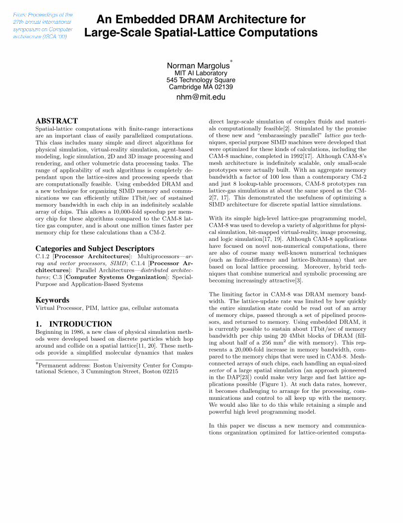
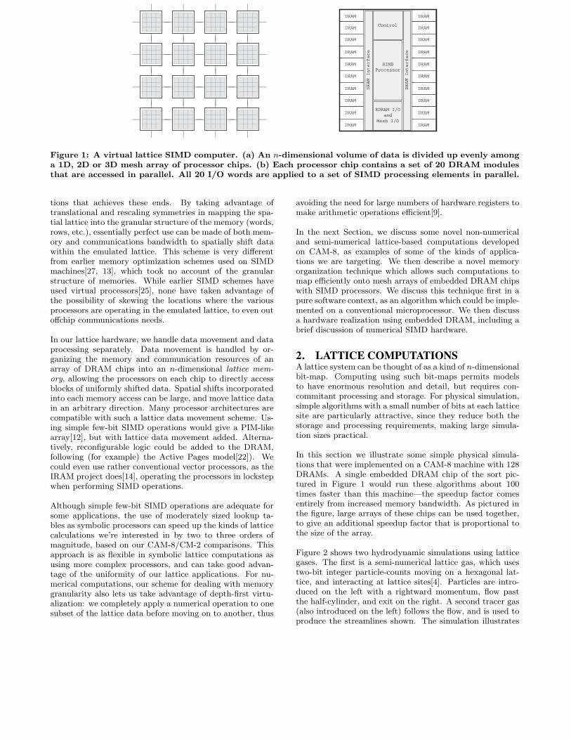
The limiting factor in CAM-8 was DRAM memory band-width. The lattice-update rate was limited by how quicklythe entire simulation state could be read out of an arrayof memory chips, passed through a set of pipelined proces-sors, and returned to memory. Using embedded DRAM, itis currently possible to sustain about 1Tbit/sec of memorybandwidth per chip using 20 4Mbit blocks of DRAM (fill-ing about half of a 256 mm2 die with memory). This rep-resents a 20,000-fold increase in memory bandwidth, com-pared to the memory chips that were used in CAM-8. Mesh-connected arrays of such chips, each handling an equal-sizedsector of a large spatial simulation (an approach pioneeredin the DAP[23]) could make very large and fast lattice ap-plications possible (Figure 1). At such data rates, however,it becomes challenging to arrange for the processing, com-munications and control to all keep up with the memory.We would also like to do this while retaining a simple andpowerful high level programming model.
In this paper we discuss a new memory and communica-tions organization optimized for lattice-oriented computa-
SIMDProcessor
Control
RDRAM I/Oand
Mesh I/O
DRAM Interface
DRAM Interface
DRAM
DRAM
DRAM
DRAM
DRAM
DRAM
DRAM
DRAM
DRAM
DRAM
DRAM
DRAM
DRAM
DRAM
DRAM
DRAM
DRAM
DRAM
DRAM
DRAM
Figure 1: A virtual lattice SIMD computer. (a) An n-dimensional volume of data is divided up evenly amonga 1D, 2D or 3D mesh array of processor chips. (b) Each processor chip contains a set of 20 DRAM modulesthat are accessed in parallel. All 20 I/O words are applied to a set of SIMD processing elements in parallel.
tions that achieves these ends. By taking advantage oftranslational and rescaling symmetries in mapping the spa-tial lattice into the granular structure of the memory (words,rows, etc.), essentially perfect use can be made of both mem-ory and communications bandwidth to spatially shift datawithin the emulated lattice. This scheme is very di"erentfrom earlier memory optimization schemes used on SIMDmachines[27, 13], which took no account of the granularstructure of memories. While earlier SIMD schemes haveused virtual processors[25], none have taken advantage ofthe possibility of skewing the locations where the variousprocessors are operating in the emulated lattice, to even outo"chip communications needs.
In our lattice hardware, we handle data movement and dataprocessing separately. Data movement is handled by or-ganizing the memory and communication resources of anarray of DRAM chips into an n-dimensional lattice mem-ory, allowing the processors on each chip to directly accessblocks of uniformly shifted data. Spatial shifts incorporatedinto each memory access can be large, and move lattice datain an arbitrary direction. Many processor architectures arecompatible with such a lattice data movement scheme. Us-ing simple few-bit SIMD operations would give a PIM-likearray[12], but with lattice data movement added. Alterna-tively, reconfigurable logic could be added to the DRAM,following (for example) the Active Pages model[22]). Wecould even use rather conventional vector processors, as theIRAM project does[14], operating the processors in lockstepwhen performing SIMD operations.
Although simple few-bit SIMD operations are adequate forsome applications, the use of moderately sized lookup ta-bles as symbolic processors can speed up the kinds of latticecalculations we’re interested in by two to three orders ofmagnitude, based on our CAM-8/CM-2 comparisons. Thisapproach is as flexible in symbolic lattice computations asusing more complex processors, and can take good advan-tage of the uniformity of our lattice applications. For nu-merical computations, our scheme for dealing with memorygranularity also lets us take advantage of depth-first virtu-alization: we completely apply a numerical operation to onesubset of the lattice data before moving on to another, thus
avoiding the need for large numbers of hardware registers tomake arithmetic operations e!cient[9].
In the next Section, we discuss some novel non-numericaland semi-numerical lattice-based computations developedon CAM-8, as examples of some of the kinds of applica-tions we are targeting. We then describe a novel memoryorganization technique which allows such computations tomap e!ciently onto mesh arrays of embedded DRAM chipswith SIMD processors. We discuss this technique first in apure software context, as an algorithm which could be imple-mented on a conventional microprocessor. We then discussa hardware realization using embedded DRAM, including abrief discussion of numerical SIMD hardware.
2. LATTICE COMPUTATIONSA lattice system can be thought of as a kind of n-dimensionalbit-map. Computing using such bit-maps permits modelsto have enormous resolution and detail, but requires con-commitant processing and storage. For physical simulation,simple algorithms with a small number of bits at each latticesite are particularly attractive, since they reduce both thestorage and processing requirements, making large simula-tion sizes practical.
In this section we illustrate some simple physical simula-tions that were implemented on a CAM-8 machine with 128DRAMs. A single embedded DRAM chip of the sort pic-tured in Figure 1 would run these algorithms about 100times faster than this machine—the speedup factor comesentirely from increased memory bandwidth. As pictured inthe figure, large arrays of these chips can be used together,to give an additional speedup factor that is proportional tothe size of the array.
Figure 2 shows two hydrodynamic simulations using latticegases. The first is a semi-numerical lattice gas, which usestwo-bit integer particle-counts moving on a hexagonal lat-tice, and interacting at lattice sites[4]. Particles are intro-duced on the left with a rightward momentum, flow pastthe half-cylinder, and exit on the right. A second tracer gas(also introduced on the left) follows the flow, and is used toproduce the streamlines shown. The simulation illustrates
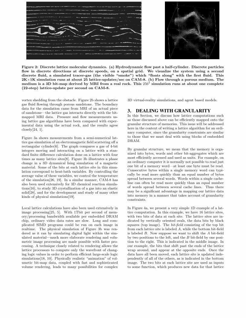
Figure 2: Discrete lattice molecular dynamics. (a) Hydrodynamic flow past a half-cylinder. Discrete particlesflow in discrete directions at discrete speeds, on a spatial grid. We visualize the system using a seconddiscrete fluid, a simulated tracer-gas (the visible “smoke”) which “floats along” with the first fluid. This2K"1K simulation runs at about 25 lattice-updates/sec on CAM-8. (b) Flow through a porous medium. Themedium is a 3D bit-map derived by MRI from a real rock. This 2563 simulation runs at about one complete(22-step) lattice-update per second on CAM-8.
vortex shedding from the obstacle. Figure 2b shows a latticegas fluid flowing through porous sandstone. The boundarydata for the simulation came from MRI of an actual pieceof sandstone—the lattice gas interacts directly with the bit-mapped MRI data. Pressure and flow measurements us-ing lattice gas algorithms have been compared with exper-imental data using the actual rock, and the results agreeclosely[24, 1].
Figure 3a shows measurements from a semi-numerical lat-tice gas simulation of an electromagnetic field scattering o" arectangular cylinder[6]. The graph compares a gas of 4-bitintegers moving and interacting on a lattice with a stan-dard finite di"erence calculation done on a lattice with fourtimes as many lattice sites[8]. Figure 3b illustrates a phasechange in a 3D dynamical Ising simulation of a magneticmaterial. Some of the bits at each lattice site in this simu-lation correspond to heat-bath variables. By controlling theaverage value of these variables, we control the temperatureof the simulation[26, 19]. In a similar manner, CAM-8 hasalso been used extensively for 3D chemical reaction simula-tions[16], to study 3D crystallization of a gas into an elasticsolid[28], and for the development and study of many otherkinds of physical simulations[19].
Local lattice calculations have also been used extensively inimage processing[25, 5]. With 1Tbit per second of mem-ory/processing bandwidth available per embedded DRAMchip, ordinary video data rates are slow. Long and com-plicated SIMD programs could be run on each image inrealtime. The physical simulation of Figure 3b was ren-dered as it ran by simulating digital light within the sim-ulated material—much more elaborate rendering and volu-metric image processing are made possible with faster pro-cessing. A technique closely related to rendering allows thelattice processors to compute only the wavefront of chang-ing logic values in order to perform e!cient large-scale logicsimulations[18, 10]. Physically realistic “animation” of vol-umetic bit-map data, coupled with fast and sophisticatedvolume rendering, leads to many possibilities for complex
3D virtual-reality simulations, and agent based models.
3. DEALINGWITH GRANULARITYIn this Section, we discuss how lattice computations suchas those discussed above can be e!ciently mapped onto thegranular structure of memories. This issue will be addressedhere in the context of writing a lattice algorithm for an ordi-nary computer, since the granularity constraints are similarto those that we must deal with using blocks of embeddedDRAM.
By granular structure, we mean that the memory is orga-nized into bytes, words and other bit-aggregates which aremost e!ciently accessed and used as units. For example, onan ordinary computer it is normally not possible to read justone bit of a memory word—at least one byte must be read.Consecutive bytes within a single memory word can typi-cally be read more quickly than an equal number of bytesspread between several words. Words within a single cache-line can often be read more quickly than an equal numberof words spread between several cache lines. Thus theremay be a significant advantage in mapping our lattice datainto memory in a manner that takes account of granularityconstraints.
In Figure 4a, we present a very simple 1D example of a lat-tice computation. In this example, we have 16 lattice sites,with two bits of data at each site. The lattice sites are in-dicated by vertically oriented ovals, the data bits by blacksquares (top image). The bit-field consisting of the top bitfrom each lattice site is labeled A, while the bottom bit-fieldis labeled B. Now suppose we want to shift the A bit-fieldby two positions to the left, and the B bit-field by one posi-tion to the right. This is indicated in the middle image. Inour example, the bits that shift past the ends of the latticewrap around, and appear at the opposite ends. Once thedata have all been moved, each lattice site is updated inde-pendently of all of the others, as is indicated in the bottomimage. The two bits at each lattice site are used as inputsto some function, which produces new data for that lattice
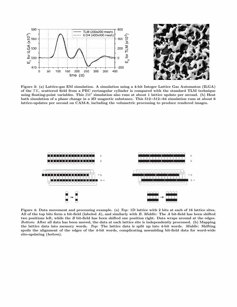
Figure 3: (a) Lattice-gas EM simulation. A simulation using a 4-bit Integer Lattice Gas Automaton (ILGA)of the TEz scattered field from a PEC rectangular cylinder is compared with the standard TLM techniqueusing floating-point variables. This 2563 simulation also runs at about 1 lattice update per second. (b) Heatbath simulation of a phase change in a 3D magnetic substance. This 512"512"64 simulation runs at about 6lattice-updates per second on CAM-8, including the volumetric processing to produce rendered images.
A
B
A
B
’
A
B
A
B
’ ’ ’ ’
Figure 4: Data movement and processing example. (a) Top: 1D lattice with 2 bits at each of 16 lattice sites.All of the top bits form a bit-field (labeled A), and similarly with B. Middle: The A bit-field has been shiftedtwo positions left, while the B bit-field has been shifted one position right. Data wraps around at the edges.Bottom: After all data has been moved, the data at each lattice site is independently processed. (b) Mappingthe lattice data into memory words. Top: The lattice data is split up into 4-bit words. Middle: Shiftingspoils the alignment of the edges of the 4-bit words, complicating assembling bit-field data for word-widesite-updating (bottom).
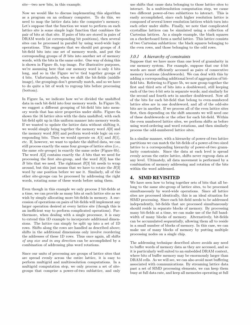
site—two new bits, in this example.
Now we would like to discuss implementing this algorithmas a program on an ordinary computer. To do this, weneed to map the lattice data into the computer’s memory.Let’s suppose that the function we want to perform on eachlattice site is some simple logic function that combines thepair of bits at that site. If pairs of bits are stored in pairs ofDRAM words (at corresponding bit positions), then severalsites can be processed in parallel by using word-wide logicoperations. This suggests that we should put groups of Abit-field bits into one set of memory words, and put thecorresponding groups of B bits into another set of memorywords, with the bits in the same order. One way of doing thisis shown in Figure 4b, top image. For illustrative purposes,we’re assuming here that our memory word is only 4 bitslong, and so in the Figure we’ve tied together groups of4 bits. Unfortunately, when we shift the bit-fields (middleimage), the groupings don’t generally match, and so we haveto do quite a bit of work to regroup bits before processing(bottom).
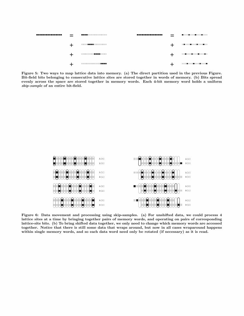
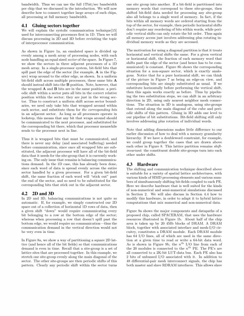
In Figure 5a, we indicate how we’ve divided the unshifteddata in each bit-field into four memory words. In Figure 5b,we suggest a di"erent grouping of bit-field bits into mem-ory words that has nicer properties under shifts. Figure 6ashows the 16 lattice sites with the data unshifted, with eachbit-field split up in this uniform manner into memory words.If we wanted to update the lattice data without shifting it,we would simply bring together the memory word A[0] andthe memory word B[0] and perform word-wide logic on cor-responding bits. Then we would operate on A[1] and B[1],etc. If, however, we want to update the shifted data, we canstill process exactly the same four groups of lattice sites (i.e.,the same site-groups) in exactly the same order (Figure 6b).The word A[2] contains exactly the A bits that we need forprocessing the first site-group, and the word B[3] has theB bits that we need. The rightmost B[3] bit needs to wraparound, but this just means that we have to rotate the B[3]word by one position before we use it. Similarly, all of theother site-groups can be processed by addressing the rightwords, rotating some of these words before using them.
Even though in this example we only process 2 bit-fields ata time, we can provide as many bits at each lattice site as wewish by simply allocating more bit-fields in memory. A suc-cession of operations on pairs of bit-fields will implement anylarger operation desired at every lattice site (though this isan ine!cient way to perform complicated operations). Fur-thermore, when dealing with a single processor, it is easyto extend this 1D example to incorporate additional dimen-sions. The lattice can simply be split up into a set of 1Drows. Shifts along the rows are handled as described above;shifts in the additional dimensions only involve reorderingthe addresses of these 1D rows. Thus once again, all shiftsof any size and in any direction can be accomplished by acombination of addressing plus word rotations.
Since our units of processing are groups of lattice sites thatare spread evenly across the entire lattice, it is easy toperform multigrid and multiresolution computations. In amultigrid computation step, we only process a set of site-groups that comprise a power-of-two sublattice, and only
use shifts that cause data belonging to those lattice sites tointeract. In a multiresolution computation step, we causetwo di"erent power-of-two sublattices to interact. This iseasily accomplished, since each higher resolution lattice iscomposed of several lower resolution lattices which turn intoeach other under shifts. Finally, we note that complicatedcrystalline lattices can be simulated using a collection ofCartesian lattices. As a simple example, the black squareson a checkerboard form a useful lattice. This lattice consistsof two Cartesian sublattices: the black squares belonging tothe even rows, and those belonging to the odd rows.
3.0.1 A hierarchy of constraintsSuppose that we have more than one level of granularity inour memory system. For example, suppose that our 4-bitwords are most e!ciently accessed as pairs of consecutivememory locations (doublewords). We can deal with this byadding a corresponding additional level of aggregation of bit-field bits. Referring to Figure 5b, we now group together thefirst and third sets of bits into a doubleword, still keepingeach of the two 4-bit sets in separate words; and similarly forthe second and fourth sets in another doubleword. Now allof the bits for each bit-field that belong to even-numberedlattice sites are in one doubleword, and all of the odd-sitebits are in another. If we process all of the even lattice sitesfirst, then depending on the shift amounts we will need oneof these doublewords or the other for each bit-field. Withinthe even numbered lattice sites, we perform shifts as beforeusing word-ordering and word rotations, and then similarlyprocess the odd-numbered lattice sites.
In a similar manner, with a hierarchy of power-of-two latticepartitions we can match the bit-fields of a power-of-two sizedlattice to a corresponding hierarchy of power-of-two granu-larity constraints. Since the data at each level is spreadevenly across the entire lattice, shifts never regroup data atany level. Ultimately, all data movement is performed by acombination of memory addressing and rotation of the bitswithin the word addressed.
4. SIMD REVISITEDWe have seen how to bring together sets of bits that all be-long to the same site-group of lattice sites, to be processedsimultaneously by word-wide operations. Since all latticesites are processed identically, this is an ideal situation forSIMD processing. Since each bit-field needs to be addressedindependently, bit-fields that are processed simultaneouslyshould reside in separate blocks of memory. By processingmany bit-fields at a time, we can make use of the full band-width of many blocks of memory. Alternatively, bit-fieldscan be accumulated sequentially, allowing them all to residein a small number of blocks of memory. In this case, we canmake use of many blocks of memory by putting multipleprocessing nodes on a single chip.
The addressing technique described above avoids any needto bu"er words of memory data as they are accessed, and soit is particularly well suited to an embedded DRAM context,where bits of bu"er memory may be enormously larger thanDRAM cells. As we will see, we can also avoid most bu"eringassociated with communications. By streaming lattice datapast a set of SIMD processing elements, we can keep thembusy at full data rate, and keep all memories operating at full
+
++
= =+
++
Figure 5: Two ways to map lattice data into memory. (a) The direct partition used in the previous Figure.Bit-field bits belonging to consecutive lattice sites are stored together in words of memory. (b) Bits spreadevenly across the space are stored together in memory words. Each 4-bit memory word holds a uniformskip-sample of an entire bit-field.
A[0]
B[0]
A[1]
B[1]
A[2]
B[2]
A[3]
B[3]
B[3]
A[0]
B[0]
A[1]
B[1]
A[2]
B[2]
A[3]
Figure 6: Data movement and processing using skip-samples. (a) For unshifted data, we could process 4lattice sites at a time by bringing together pairs of memory words, and operating on pairs of correspondinglattice-site bits. (b) To bring shifted data together, we only need to change which memory words are accessedtogether. Notice that there is still some data that wraps around, but now in all cases wraparound happenswithin single memory words, and so each data word need only be rotated (if necessary) as it is read.
bandwidth. Thus we can use the full 1Tbit/sec bandwidthper chip that we discussed in the introduction. We will nowdescribe how to connect together large arrays of such chips,all processing at full memory bandwidth.
4.1 Gluing sectors togetherWe will explain the systolic communication technique[15]used for interconnecting processors first in 1D. Then we willdiscuss processing in 2D and 3D before revisiting the topicof interprocessor communication.
As shown in Figure 1a, an emulated space is divided upevenly among a mesh array of processing nodes, with eachnode handling an equal sized sector of the space. In Figure 7,we show the sectors in three adjacent processors of a 1Dmesh array. In a single-processor system, bit-field bits thatspill past the edge of the sector (for example, A in the Fig-ure) wrap around to the other edge, as shown. In a uniformbit-field shift across multiple processors, these same bits Ashould instead shift into the B position. Note, however, thatthe wrapped A and B bits are in the same position: a peri-odic shift within a sector puts all bits in the correct relativeposition within the sector; they are just in the wrong sec-tor. Thus to construct a uniform shift across sector bound-aries, we need only take bits that wrapped around withineach sector, and substitute them for the corresponding bitsin an adjacent sector. As long as all processors operate inlockstep, this means that any bit that wraps around shouldbe communicated to the next processor, and substituted forthe corresponding bit there, which that processor meanwhilesends to the processor next in line.
Thus it is wrapped bits that must be communicated, andthere is never any delay (and associated bu"ering) neededbefore communication, since once all wrapped bits are sub-stituted, the adjacent processor will have all of the bit-fielddata that it needs for the site-group that it is currently work-ing on. The only issue that remains is balancing communica-tions demand. In the 1D case, this has already been done,since each word of data is spread evenly across the entiresector handled by a given processor. For a given bit-fieldshift, the same fraction of each word will “stick out” pastthe end of the sector, and so need to be substituted for thecorresponding bits that stick out in the adjacent sector.
4.2 2D and 3DIn 2D and 3D, balancing communications is not quite soautomatic. If, for example, we simply constructed our 2Dspace out of a collection of horizontal 1D rows of data, thena given shift “down” would require communicating everybit belonging to a row at the bottom edge of the sector;whereas when processing a row that doesn’t spill past thebottom edge, we would require no communication—thus thecommunication demand in the vertical direction would notbe very even in time.
In Figure 8a, we show a way of partitioning a square 2D lat-tice (and hence all of the bit fields) so that communicationsdemand is even in time. Recall that a site-group is a set oflattice sites that are processed together. In this example, westretch one site-group evenly along the main diagonal of thesector. The other site-groups are then periodic shifts of thispattern. Clearly any periodic shift within the sector turns
one site group into another. If a bit-field is partitioned intomemory words that correspond to these site-groups, thenshifted bit-field data needed for processing any site-groupalso all belongs to a single word of memory. In fact, if thebits within all memory words are ordered starting from thetop of the sector, for example, then periodic horizontal shiftsdon’t require any reordering of bits within words, while peri-odic vertical shifts can only rotate the bit order. Thus againall memory access just involves addressing plus rotating in-dividual memory words as they are accessed.
The motivation for using a diagonal partition is that it treatshorizontal and vertical shifts the same. For a given verticalor horizontal shift, the fraction of each memory word thatshifts past the edge of the sector (and hence has to be com-municated) is constant. Figure 8b shows the correspondingsituation for a non-square sector, which is exactly analo-gous. Notice that for a pure horizontal shift, we can thinkof the picture in Figure 7 as being an edge-on view, andcorresponding bits are simply substituted as usual. If wesubstitute horizontally before performing the vertical shift,then this again works exactly as before. Thus by pipelin-ing the two substitution steps, we can shift in an arbitrarydirection in 2D, using only nearest neighbor mesh connec-tions. The situation in 3D is analogous, using site-groupsthat extend along the main diagonal of the cube and peri-odic shifts of this pattern. Gluing in 3D adds one level toour pipeline of bit substitutions. Bit-field shifting still onlyinvolves addressing plus rotation of individual words.
Note that adding dimensions makes little di"erence to ourearlier discussion of how to deal with a memory granularityhierarchy. If we have a doubleword constraint, for example,we could group together the cases that are drawn aboveeach other in Figure 8. This lattice partition remains shift-invariant: the constituent double site-groups turn into eachother under shifts.
4.3 HardwareThe shifting and communication technique described aboveis suitable for a variety of spatial lattice architectures, withvarious kinds of SIMD processing elements and various num-bers of simultaneously shifting bit-fields coupled to each PE.Here we describe hardware that is well suited for the kindsof non-numerical and semi-numerical simulations discussedin Section 2. We will also discuss in Section 4.4 how tomodify this hardware, in order to adapt it to hybrid latticecomputations that mix numerical and non-numerical data.
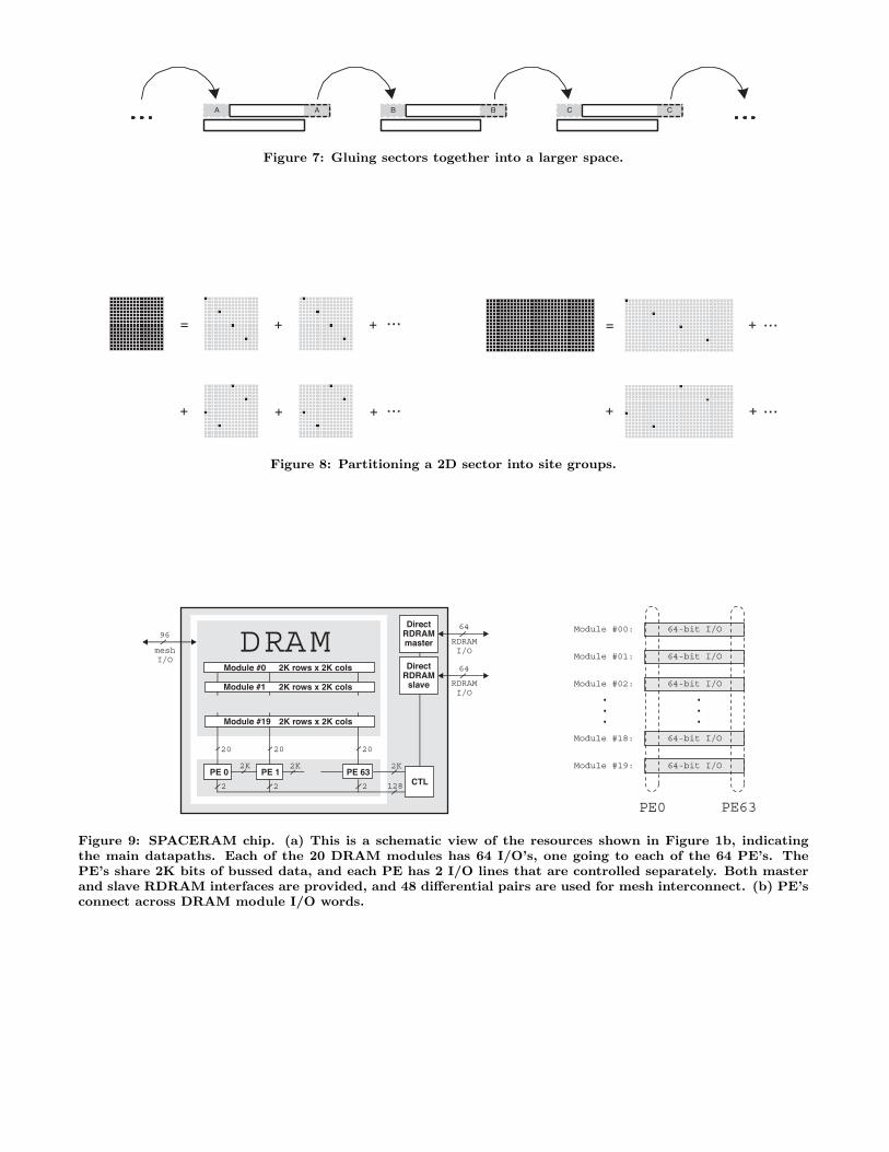
Figure 9a shows the major components and datapaths of aproposed chip, called SPACERAM, that uses the hardwareresources illustrated in Figure 1b. About half of the chiparea is taken up by 20 4Mb blocks of DRAM. A DRAMblock, together with associated interface and mesh-I/O cir-cuitry, constitutes a DRAM module. Each DRAM modulehas 64 I/O lines, all of which are used in the same direc-tion at a given time to read or write a 64-bit data word.As is shown in Figure 9b, the nth I/O line from each ofthe 20 modules is connected to the nth PE. The PE’s areall connected to a 2K-bit LUT-data bus. Each PE also has2 bits of unbussed I/O associated with it. In addition to48 di"erential-pair mesh interconnect signals, the chip hasboth master and slave RDRAM interfaces. This allows slave
AA BB CC
Figure 7: Gluing sectors together into a larger space.
= + + ...
+ + ...+
= + ...
++ ...
Figure 8: Partitioning a 2D sector into site groups.
DRAMModule #0 2K rows x 2K cols
PE 0 PE 1 PE 63
20 2020
Module #19
Module #1 2K rows x 2K cols
2K rows x 2K cols
2K 2K 2K
128
96
meshI/O
DirectRDRAM
slave
64
RDRAMI/O
CTL
DirectRDRAMmaster
64
RDRAMI/O
2 2 2
64-bit I/O
64-bit I/O
64-bit I/O
64-bit I/O
64-bit I/OModule #00:
Module #01:
Module #02:
Module #18:
Module #19:
...
...
PE0 PE63
Figure 9: SPACERAM chip. (a) This is a schematic view of the resources shown in Figure 1b, indicatingthe main datapaths. Each of the 20 DRAM modules has 64 I/O’s, one going to each of the 64 PE’s. ThePE’s share 2K bits of bussed data, and each PE has 2 I/O lines that are controlled separately. Both masterand slave RDRAM interfaces are provided, and 48 di!erential pairs are used for mesh interconnect. (b) PE’sconnect across DRAM module I/O words.
RDRAM’s to be attached to each chip, in order to increasethe size of simulations that can be run, and also allows thechip to be directly connected to a microprocessor that hasan RDRAM master interface.
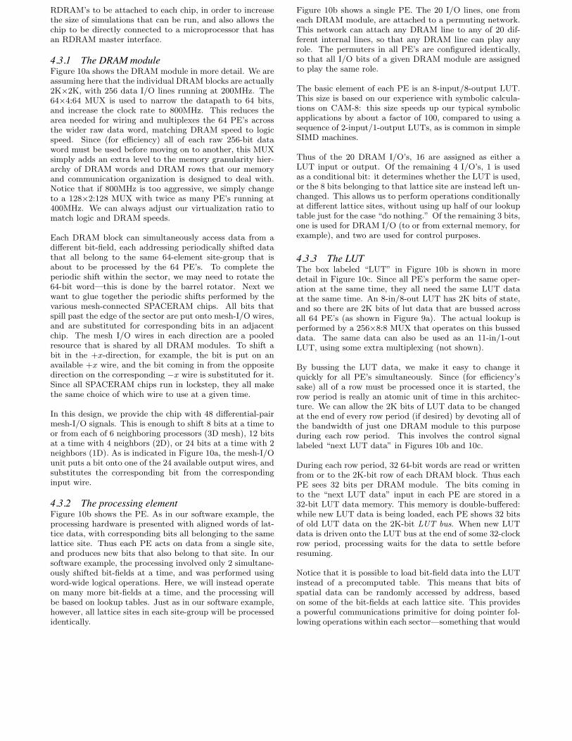
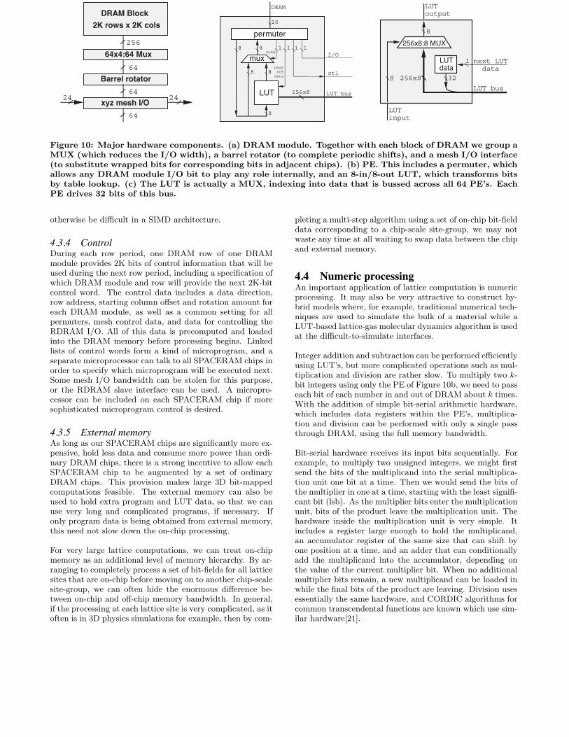
4.3.1 The DRAM moduleFigure 10a shows the DRAM module in more detail. We areassuming here that the individual DRAM blocks are actually2K"2K, with 256 data I/O lines running at 200MHz. The64"4:64 MUX is used to narrow the datapath to 64 bits,and increase the clock rate to 800MHz. This reduces thearea needed for wiring and multiplexes the 64 PE’s acrossthe wider raw data word, matching DRAM speed to logicspeed. Since (for e!ciency) all of each raw 256-bit dataword must be used before moving on to another, this MUXsimply adds an extra level to the memory granularity hier-archy of DRAM words and DRAM rows that our memoryand communication organization is designed to deal with.Notice that if 800MHz is too aggressive, we simply changeto a 128"2:128 MUX with twice as many PE’s running at400MHz. We can always adjust our virtualization ratio tomatch logic and DRAM speeds.
Each DRAM block can simultaneously access data from adi"erent bit-field, each addressing periodically shifted datathat all belong to the same 64-element site-group that isabout to be processed by the 64 PE’s. To complete theperiodic shift within the sector, we may need to rotate the64-bit word—this is done by the barrel rotator. Next wewant to glue together the periodic shifts performed by thevarious mesh-connected SPACERAM chips. All bits thatspill past the edge of the sector are put onto mesh-I/O wires,and are substituted for corresponding bits in an adjacentchip. The mesh I/O wires in each direction are a pooledresource that is shared by all DRAM modules. To shift abit in the +x-direction, for example, the bit is put on anavailable +x wire, and the bit coming in from the oppositedirection on the corresponding #x wire is substituted for it.Since all SPACERAM chips run in lockstep, they all makethe same choice of which wire to use at a given time.
In this design, we provide the chip with 48 di"erential-pairmesh-I/O signals. This is enough to shift 8 bits at a time toor from each of 6 neighboring processors (3D mesh), 12 bitsat a time with 4 neighbors (2D), or 24 bits at a time with 2neighbors (1D). As is indicated in Figure 10a, the mesh-I/Ounit puts a bit onto one of the 24 available output wires, andsubstitutes the corresponding bit from the correspondinginput wire.
4.3.2 The processing elementFigure 10b shows the PE. As in our software example, theprocessing hardware is presented with aligned words of lat-tice data, with corresponding bits all belonging to the samelattice site. Thus each PE acts on data from a single site,and produces new bits that also belong to that site. In oursoftware example, the processing involved only 2 simultane-ously shifted bit-fields at a time, and was performed usingword-wide logical operations. Here, we will instead operateon many more bit-fields at a time, and the processing willbe based on lookup tables. Just as in our software example,however, all lattice sites in each site-group will be processedidentically.
Figure 10b shows a single PE. The 20 I/O lines, one fromeach DRAM module, are attached to a permuting network.This network can attach any DRAM line to any of 20 dif-ferent internal lines, so that any DRAM line can play anyrole. The permuters in all PE’s are configured identically,so that all I/O bits of a given DRAM module are assignedto play the same role.
The basic element of each PE is an 8-input/8-output LUT.This size is based on our experience with symbolic calcula-tions on CAM-8: this size speeds up our typical symbolicapplications by about a factor of 100, compared to using asequence of 2-input/1-output LUTs, as is common in simpleSIMD machines.
Thus of the 20 DRAM I/O’s, 16 are assigned as either aLUT input or output. Of the remaining 4 I/O’s, 1 is usedas a conditional bit: it determines whether the LUT is used,or the 8 bits belonging to that lattice site are instead left un-changed. This allows us to perform operations conditionallyat di"erent lattice sites, without using up half of our lookuptable just for the case “do nothing.” Of the remaining 3 bits,one is used for DRAM I/O (to or from external memory, forexample), and two are used for control purposes.
4.3.3 The LUTThe box labeled “LUT” in Figure 10b is shown in moredetail in Figure 10c. Since all PE’s perform the same oper-ation at the same time, they all need the same LUT dataat the same time. An 8-in/8-out LUT has 2K bits of state,and so there are 2K bits of lut data that are bussed acrossall 64 PE’s (as shown in Figure 9a). The actual lookup isperformed by a 256"8:8 MUX that operates on this busseddata. The same data can also be used as an 11-in/1-outLUT, using some extra multiplexing (not shown).
By bussing the LUT data, we make it easy to change itquickly for all PE’s simultaneously. Since (for e!ciency’ssake) all of a row must be processed once it is started, therow period is really an atomic unit of time in this architec-ture. We can allow the 2K bits of LUT data to be changedat the end of every row period (if desired) by devoting all ofthe bandwidth of just one DRAM module to this purposeduring each row period. This involves the control signallabeled “next LUT data” in Figures 10b and 10c.
During each row period, 32 64-bit words are read or writtenfrom or to the 2K-bit row of each DRAM block. Thus eachPE sees 32 bits per DRAM module. The bits coming into the “next LUT data” input in each PE are stored in a32-bit LUT data memory. This memory is double-bu"ered:while new LUT data is being loaded, each PE shows 32 bitsof old LUT data on the 2K-bit LUT bus. When new LUTdata is driven onto the LUT bus at the end of some 32-clockrow period, processing waits for the data to settle beforeresuming.
Notice that it is possible to load bit-field data into the LUTinstead of a precomputed table. This means that bits ofspatial data can be randomly accessed by address, basedon some of the bit-fields at each lattice site. This providesa powerful communications primitive for doing pointer fol-lowing operations within each sector—something that would
DRAM Block2K rows x 2K cols
256
64
Barrel rotator64
xyz mesh I/O64
24 24
64x4:64 Mux
LUT
88 1
8
8
1 1 1
256x8
permuter20
8
I/O
ctl
LUT bus
DRAM
cond
nextLUT
data
mux
256x8
8
LUT bus
256x8:8 MUX
LUTdata328
1 next LUTdata
LUT input
LUT output
Figure 10: Major hardware components. (a) DRAM module. Together with each block of DRAM we group aMUX (which reduces the I/O width), a barrel rotator (to complete periodic shifts), and a mesh I/O interface(to substitute wrapped bits for corresponding bits in adjacent chips). (b) PE. This includes a permuter, whichallows any DRAM module I/O bit to play any role internally, and an 8-in/8-out LUT, which transforms bitsby table lookup. (c) The LUT is actually a MUX, indexing into data that is bussed across all 64 PE’s. EachPE drives 32 bits of this bus.
otherwise be di!cult in a SIMD architecture.
4.3.4 ControlDuring each row period, one DRAM row of one DRAMmodule provides 2K bits of control information that will beused during the next row period, including a specification ofwhich DRAM module and row will provide the next 2K-bitcontrol word. The control data includes a data direction,row address, starting column o"set and rotation amount foreach DRAM module, as well as a common setting for allpermuters, mesh control data, and data for controlling theRDRAM I/O. All of this data is precomputed and loadedinto the DRAM memory before processing begins. Linkedlists of control words form a kind of microprogram, and aseparate microprocessor can talk to all SPACERAM chips inorder to specify which microprogram will be executed next.Some mesh I/O bandwidth can be stolen for this purpose,or the RDRAM slave interface can be used. A micropro-cessor can be included on each SPACERAM chip if moresophisticated microprogram control is desired.
4.3.5 External memoryAs long as our SPACERAM chips are significantly more ex-pensive, hold less data and consume more power than ordi-nary DRAM chips, there is a strong incentive to allow eachSPACERAM chip to be augmented by a set of ordinaryDRAM chips. This provision makes large 3D bit-mappedcomputations feasible. The external memory can also beused to hold extra program and LUT data, so that we canuse very long and complicated programs, if necessary. Ifonly program data is being obtained from external memory,this need not slow down the on-chip processing.
For very large lattice computations, we can treat on-chipmemory as an additional level of memory hierarchy. By ar-ranging to completely process a set of bit-fields for all latticesites that are on-chip before moving on to another chip-scalesite-group, we can often hide the enormous di"erence be-tween on-chip and o"-chip memory bandwidth. In general,if the processing at each lattice site is very complicated, as itoften is in 3D physics simulations for example, then by com-
pleting a multi-step algorithm using a set of on-chip bit-fielddata corresponding to a chip-scale site-group, we may notwaste any time at all waiting to swap data between the chipand external memory.
4.4 Numeric processingAn important application of lattice computation is numericprocessing. It may also be very attractive to construct hy-brid models where, for example, traditional numerical tech-niques are used to simulate the bulk of a material while aLUT-based lattice-gas molecular dynamics algorithm is usedat the di!cult-to-simulate interfaces.
Integer addition and subtraction can be performed e!cientlyusing LUT’s, but more complicated operations such as mul-tiplication and division are rather slow. To multiply two k-bit integers using only the PE of Figure 10b, we need to passeach bit of each number in and out of DRAM about k times.With the addition of simple bit-serial arithmetic hardware,which includes data registers within the PE’s, multiplica-tion and division can be performed with only a single passthrough DRAM, using the full memory bandwidth.
Bit-serial hardware receives its input bits sequentially. Forexample, to multiply two unsigned integers, we might firstsend the bits of the multiplicand into the serial multiplica-tion unit one bit at a time. Then we would send the bits ofthe multiplier in one at a time, starting with the least signifi-cant bit (lsb). As the multiplier bits enter the multiplicationunit, bits of the product leave the multiplication unit. Thehardware inside the multiplication unit is very simple. Itincludes a register large enough to hold the multiplicand,an accumulator register of the same size that can shift byone position at a time, and an adder that can conditionallyadd the multiplicand into the accumulator, depending onthe value of the current multiplier bit. When no additionalmultiplier bits remain, a new multiplicand can be loaded inwhile the final bits of the product are leaving. Division usesessentially the same hardware, and CORDIC algorithms forcommon transcendental functions are known which use sim-ilar hardware[21].
site-group #30, bit-field #0
site-group #2, bit-field #0
site-group #1, bit-field #0
site-group #0, bit-field #0
site-group #31, bit-field #0Word #31:
Word #30:
Word #2:
Word #1:
Word #0:
...
...
PE0bit#0
PE63bit#0
site-group #0, bit-field #30
site-group #0, bit-field #2
site-group #0, bit-field #1
site-group #0, bit-field #0
site-group #0, bit-field #31Word #31:
Word #30:
Word #2:
Word #1:
Word #0:
...
...
PE0bit#0
PE63bit#0
msb
lsb
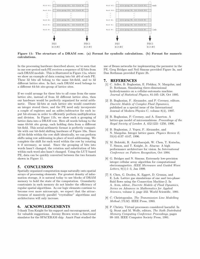
Figure 11: The structure of a DRAM row. (a) Format for symbolic calculations. (b) Format for numericcalculations.
In the processing hardware described above, we’ve seen thatin one row-period each PE receives a sequence of 32 bits fromeach DRAM module. This is illustrated in Figure 11a, wherewe show an example of data coming into bit #0 of each PE.These 32 bits all belong to the same bit-field, and to 32di"erent lattice sites. In fact, each DRAM word belongs toa di"erent 64-bit site-group of lattice sites.
If we could arrange for these bits to all come from the samelattice site, instead of from 32 di"erent lattice sites, thenour hardware would be perfectly organized for serial arith-metic. These 32-bits at each lattice site would constitutean integer stored there, and the PE need only incorporatea couple of registers and an adder/subtractor for each in-put bit-stream in order to e!ciently perform multiplicationand division. In Figure 11b, we show such a grouping oflattice data into a DRAM row. Here all words belong to thesame 64-bit site group, each holding data from a di"erentbit-field. This serial-arithmetic format is perfectly compati-ble with our bit-field shifting hardware of Figure 10a. Sinceall bit-fields within the row shift identically, we can performshifts using row addressing in place of word addresssing. Wecomplete the shift for each word within the row by rotatingit if necessary, as usual. Since the grouping of bits intowords hasn’t changed, the rotation and substitution of bitswithin each word also hasn’t changed. Using the LUT-basedPE, data can be quickly converted between the two formatsshown in Figure 11.
5. CONCLUSIONSSpatially organized computation maps naturally onto spatialarrays of processing elements. For greatest density of infor-mation storage, it is natural today to use blocks of DRAMmemory to hold the state of the computation. Granularityconstraints in such memory do not hinder the e!ciency ofregular spatial algorithms. As our logic elements continue tobecome ever more microscopic, we expect that the attrac-tiveness of massively parallel “crystalline” algorithms andarchitectures will only increase.
6. ACKNOWLEDGEMENTSI thank Tom Knight for his support and encouragement, andfor valuable suggestions. Jeremy Brown wrote a functionalsimulator for the SPACERAM chip. Amrit Pant studied the
use of Benes networks for implementing the permuter in thePE. Greg Bridges and Neil Simons provided Figure 3a, andDan Rothman provided Figure 2b.
7. REFERENCES[1] C. Adler, B. Boghosian, E. Flekkoy, N. Margolus, and
D. Rothman. Simulating three-dimensionalhydrodynamics on a cellular-automata machine.Journal of Statistical Physics, 81:105–128, Oct 1995.
[2] B. Boghosian, F. Alexander, and P. Coveney, editors.Discrete Models of Complex Fluid Dynamics,published as a special issue of the InternationalJournal of Modern Physics C, volume 8(4), 1997.
[3] B. Boghosian, P. Coveney, and A. Emerton. Alattice-gas model of microemulsions. Proceedings of theRoyal Society of London A, 452:1221–1250, 1996.
[4] B. Boghosian, J. Yepez, F. Alexander, andN. Margolus. Integer lattice gases. Physics Review E,55(4):4137–4147, 1996.
[5] M. Bolotski, R. Amirtharajah, W. Chen, T. Kutscha,T. Simon, and T. Knight, Jr. Abacus: A highperformance architecture for vision. In InternationalConference on Pattern Recognition, Oct 1994.
[6] G. Bridges and N. Simons. Extremely low-precisioninteger cellular array algorithm for computationalelectromagnetics. IEEE Microwave and Guided WaveLetters, 9(1):1–3, Jan 1999.
[7] S. Chen, G. Doolen, K. Eggert, D. Grunau, andE. Loh. Lattice gas simulations of one and two-phasefluid flows using the Connection Machine-2. InA. Aves, editor, Discrete Models of Fluid Dynamics,Series on Advances in Mathematics for AppliedSciences, volume 2, page 232. World Scientific, 1991.
[8] C. Christopoulos. The Transmission Line ModellingMethod (TLM). IEEE Press, 1993.
[9] P. Christy. Virtual processors considered harmful. InQ. Stout and M. Wolfe, editors, The Sixth DistributedMemory Computing Conference Proceedings, pages99–103. IEEE Computer Society Press, 1991.
[10] A. DeHon. Reconfigurable Architectures forGeneral-Purpose Computing. PhD thesis,Massachusetts Institute of Technology, 1996.Reprinted as MIT AI Lab Technical Report 1586.
[11] U. Frisch, B. Hasslacher, and Y. Pomeau. Lattice-gasautomata for the navier-stokes equation. PhysicsReview Letters, 56:1505–1508, 1986.
[12] M. Gokhale, B. Holmes, and K. Iobst. Processing inmemory: The terasys massively parallel PIM array.IEEE Computer, pages 24–31, Apr 1995.
[13] K. Knobe, J. Lukas, and G. Steele, Jr. Dataoptimization: Allocation of arrays to reducecommunication on SIMD machines. Journal ofParallel and Distributed Computing, 8:102–118, 1990.
[14] C. Kozyrakis, S. Perissakis, D. Patterson,T. Anderson, K. Asanovic, et al. Scalable processorsin the billion-transistor era: IRAM. IEEE Computer,pages 75–78, September 1997.
[15] H. T. Kung. Systolic communication. In Proceedingsof the International Conference on Systolic Arrays,May 1988.
[16] A. Malevanets and R. Kapral. Microscopic model forFitzhugh-Nagumo dynamics. Physics Review E,55(5):5657–5670, 1997.
[17] N. Margolus. CAM-8: A computer architecture basedon cellular automata. In A. Lawniczak and R. Kapral,editors, Pattern Formation and Lattice-Gas Automata,pages 167–187. American Mathematical Society, 1996.
[18] N. Margolus. An FPGA architecture for DRAM-basedsystolic computations. In Arnold et al., editors,Proceedings of the IEEE Workshop on FPGAs forCustom Computing Machines, pages 2–11. IEEEComputer Society Press, 1997.
[19] N. Margolus. Crystalline computation. In A. Hey,editor, Feynman and Computation, chapter 18.Perseus Books, 1999.
[20] N. Margolus, T. To"oli, and G. Vichniac.Cellular-automata supercomputers for fluid dynamicsmodeling. Physics Review Letters, 56:1694–1696, 1986.
[21] J.-M. Muller. Elementary Functions: Algorithms andImplementation. Birkhauser, 1997.
[22] M. Oskin, F. T. Chong, and T. Sherwood. Activepages: A computation model for intelligent memory.In The 25th Annual International Symposium onComputer Architecture. IEEE Computer Society, 1998.
[23] S. Reddaway. Signal processing on a processor array.In Lacoume et al., editors, Traitement Du Signal /Signal Processing, volume 2. Elsevier Science, 1987.
[24] D. Rothman and S. Zaleski. Lattice-Gas CellularAutomata—simple models of complex hydrodynamics.Cambridge University Press, 1997.
[25] S. Tanimoto and J. Pfei"er, Jr. An image processorbased on an array of pipelines. In IEEE ComputerSociety Workshop on Computer Architecture forPattern Analysis and Image Database Management,volume 81, pages 201–208, 1981.
[26] T. To"oli and N. Margolus. Cellular AutomataMachines: A New Environment for Modeling. MITPress, 1987.
[27] H. Wijsho" and J. van Leeuwen. The structure ofperiodic storage schemes for parallel memories. IEEETransactions on Computers, c-34(6):501–505, 1985.
[28] J. Yepez. Lattice-gas crystallization. Journal ofStatistical Physics, 81:255–294, 1994.