Embed Size (px)
Citation preview

Power Conversion
Version 1.2 , November 2001
Application Note
AN-CoolMOS-06
200W SMPS Demonstration Board
Author: Marko Scherf, Ilia Zverev
Published by Infineon Technologies AGhttp://www.infineon.com
� � � � � � � � � � � � � � � � � � � �

200W SMPS Demonstration Board
2 of 25 AN-CoolMOS-06V1.2
This application note describes the 200W SMPS Demonstration Board with Infineon powerproducts like CoolMOS, OptiMOS, TDA16888, SiC Schottky diode thinQ!, small signal N- & P-channel MOSFETs.
Contains
1 Features / Parameters..........................................................................................................32 General Description / Main Function ....................................................................................43 Construction / Heatsinks ......................................................................................................44 Description of Functional Part Groups..................................................................................5
4.1 Power Stages (“Main Board”) .........................................................................................54.1.1 AC input/ EMI Filter ..................................................................................................54.1.2 PFC Converter .........................................................................................................54.1.3 PWM Converter (Two Transistor Forward)...............................................................64.1.4 Synchronous Rectification ........................................................................................6
4.2 Controlling Circuitry (“Control Board”) ............................................................................64.2.1 General Description of the Combi-IC TDA16888......................................................74.2.2 PFC Control..............................................................................................................74.2.3 PWM Control ............................................................................................................74.2.4 Gate Drive Circuitry ..................................................................................................7
5 Power Losses / Efficiency ....................................................................................................86 Power Loss Sources ............................................................................................................97 Conducted EMI Measurements ..........................................................................................108 Construction of magnetic components ...............................................................................12
8.1 PFC choke....................................................................................................................128.2 Main transformer ..........................................................................................................138.3 Output filter choke ........................................................................................................14
9 PCB Layout ........................................................................................................................159.1 Main Board - Scaling 1:1 ..............................................................................................159.2 Control Board- Scaling 1:1 ...........................................................................................18
10 Bill of Materials ................................................................................................................1810.1 Main Board...................................................................................................................1810.2 Control Board ...............................................................................................................21

200W SMPS Demonstration Board
3 of 25 AN-CoolMOS-06V1.2
1 Features / Parameters
Parameters:- wide input voltage range 90-275V- output power 200W- output voltages- 5V / 20A max (load resistance = 0.25Ohm)- 12V / 8.3A max (load resistance = 1.45Ohm)- active Power Factor Correction boost converter operates at 200kHz- hard switching two transistor forward converter operates at 200kHz- synchronous rectification for 5V output operates at 200kHz
Features:- Infineon & EPCOS components on board- Second generation of CoolMOS C2 as PFC, PWM switches- Silicon Carbide (SiC) Schottky diode thinQ! as PFC diode- OptiMOS as synchronous rectification switches- PFC and PWM controller in one IC- High efficiency- No external heat sink required- No minimum output load required- Output over load protected- Output short circuit protected
200W SMPS Demonstration Board
4 of 25 AN-CoolMOS-06V1.2
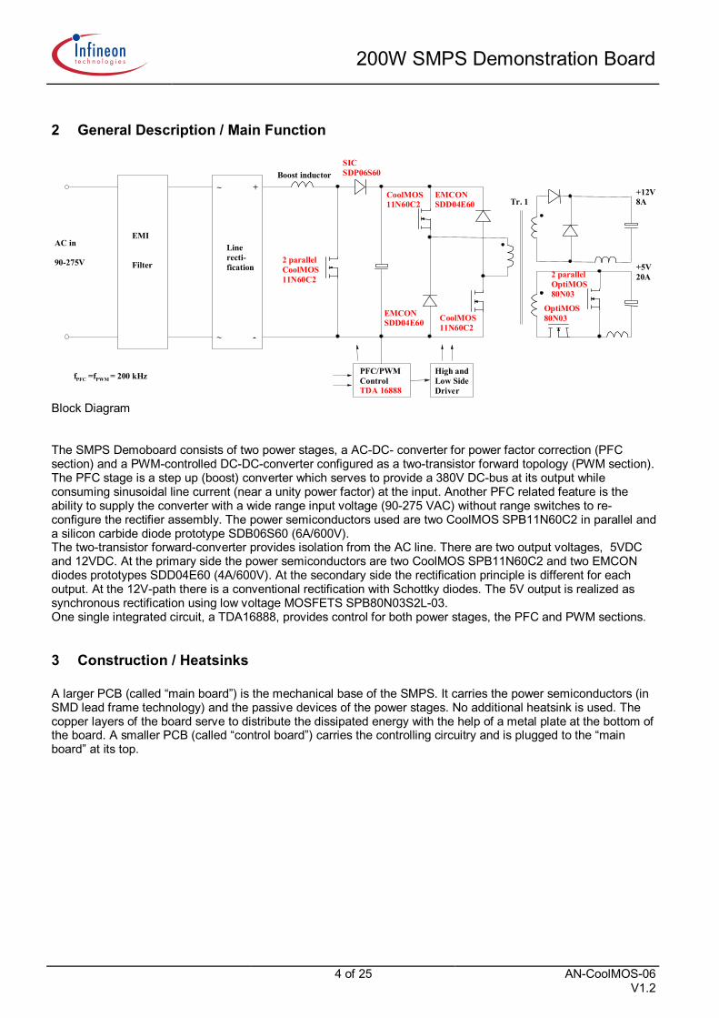
2 General Description / Main Function
Tr. 1
AC in
90-275V
EMI
Filter
Linerecti-fication
~
~ -
+Boost inductor
2 parallelCoolMOS11N60C2
SICSDP06S60
CoolMOS11N60C2
EMCONSDD04E60 CoolMOS
11N60C2
EMCONSDD04E60
OptiMOS80N03
2 parallelOptiMOS80N03
+5V20A
+12V8A
High andLow SideDriver
PFC/PWMControlTDA 16888
fPFC =fPWM = 200 kHz
Block Diagram
The SMPS Demoboard consists of two power stages, a AC-DC- converter for power factor correction (PFCsection) and a PWM-controlled DC-DC-converter configured as a two-transistor forward topology (PWM section).The PFC stage is a step up (boost) converter which serves to provide a 380V DC-bus at its output whileconsuming sinusoidal line current (near a unity power factor) at the input. Another PFC related feature is theability to supply the converter with a wide range input voltage (90-275 VAC) without range switches to re-configure the rectifier assembly. The power semiconductors used are two CoolMOS SPB11N60C2 in parallel anda silicon carbide diode prototype SDB06S60 (6A/600V).The two-transistor forward-converter provides isolation from the AC line. There are two output voltages, 5VDCand 12VDC. At the primary side the power semiconductors are two CoolMOS SPB11N60C2 and two EMCONdiodes prototypes SDD04E60 (4A/600V). At the secondary side the rectification principle is different for eachoutput. At the 12V-path there is a conventional rectification with Schottky diodes. The 5V output is realized assynchronous rectification using low voltage MOSFETS SPB80N03S2L-03.One single integrated circuit, a TDA16888, provides control for both power stages, the PFC and PWM sections.
3 Construction / Heatsinks
A larger PCB (called “main board”) is the mechanical base of the SMPS. It carries the power semiconductors (inSMD lead frame technology) and the passive devices of the power stages. No additional heatsink is used. Thecopper layers of the board serve to distribute the dissipated energy with the help of a metal plate at the bottom ofthe board. A smaller PCB (called “control board”) carries the controlling circuitry and is plugged to the “mainboard” at its top.
200W SMPS Demonstration Board
5 of 25 AN-CoolMOS-06V1.2
4 Description of Functional Part Groups
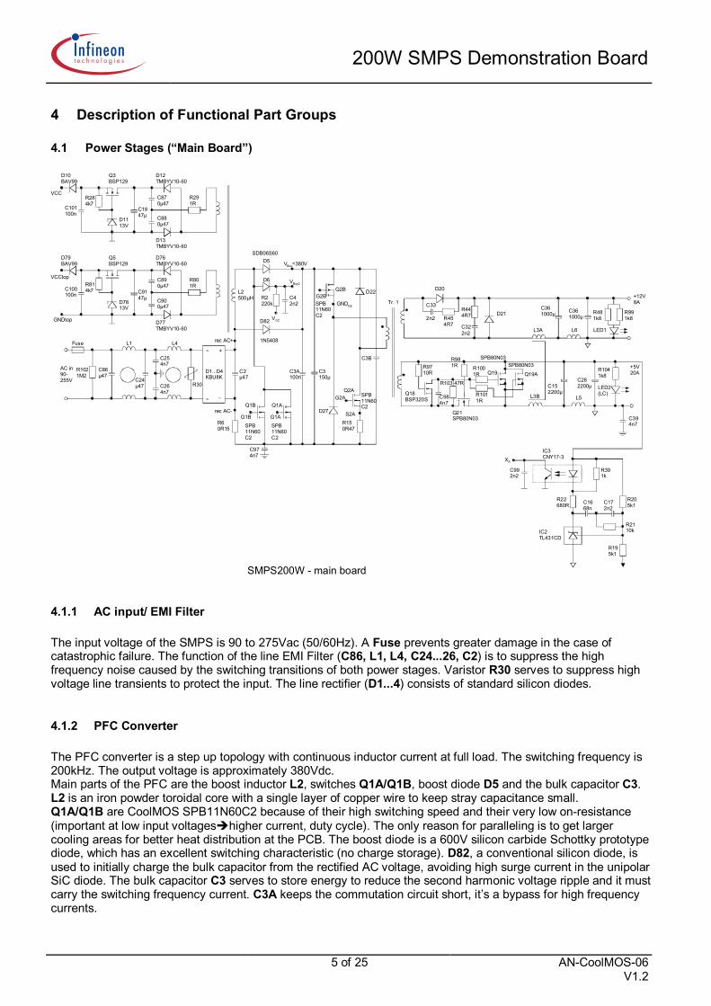
4.1 Power Stages (“Main Board”)
SMPS200W - main board
Fuse
AC in90-255V
R1021M2
L1
C86µ47
C24µ47
C254n7
C264n7
L4
R30
~
~
+
-
C2µ47
L2500µH
rec AC+
rec AC-
R60R15
Q1B
G1B
C974n7
G1A
Q1A
VCC
R2220k
C42n2
D6
D5 VBus=380V
VBus2
C3A100n
C3150µ
G2BQ2B
GNDtop
D27
D22
Q2AG2A
S2AR150R47
C3B
Tr. 1
C394n7
R9710R
R981R
C984n7
Q18BSP320S
Q21SPB80N03
R1001R
R1011R
Q19SPB80N03
Q19A
SPB80N03
L3B
L3A
D20
C33
2n2 R454R7
R444R7
C322n2
D21 R481k8
C361000µ C36
1000µ
+12V8A
+5V20A
C152200µ
C282200µ
L5
R291R
D12TMBYV10-60
D13TMBYV10-60
C870µ47
C880µ47
C1847µ
D1113V
R284k7
Q3BSP129
D10BAV99
R801R
D76TMBYV10-60
D77TMBYV10-60
C890µ47
C900µ47
C9147µ
D7813V
R814k7
Q5BSP129
D79BAV99
GNDtop
VCCtop
VCC
XS
R391k
R205k1
R2110k
C172n2
C1668n
R195k1
IC2TL431CD
R22680R
IC3CNY17-3
D1...D4KBU8K
C101100n
R991k8
R103 47R
C992n2
C100100n
D82
1N5408
SPB11N60C2
SPB11N60C2
SPB11N60C2
SPB11N60C2
R1041k8
LED2(LC)
LED1L6
SDB06S60
4.1.1 AC input/ EMI Filter
The input voltage of the SMPS is 90 to 275Vac (50/60Hz). A Fuse prevents greater damage in the case ofcatastrophic failure. The function of the line EMI Filter (C86, L1, L4, C24...26, C2) is to suppress the highfrequency noise caused by the switching transitions of both power stages. Varistor R30 serves to suppress highvoltage line transients to protect the input. The line rectifier (D1...4) consists of standard silicon diodes.
4.1.2 PFC Converter
The PFC converter is a step up topology with continuous inductor current at full load. The switching frequency is200kHz. The output voltage is approximately 380Vdc.Main parts of the PFC are the boost inductor L2, switches Q1A/Q1B, boost diode D5 and the bulk capacitor C3.L2 is an iron powder toroidal core with a single layer of copper wire to keep stray capacitance small.Q1A/Q1B are CoolMOS SPB11N60C2 because of their high switching speed and their very low on-resistance(important at low input voltages�higher current, duty cycle). The only reason for paralleling is to get largercooling areas for better heat distribution at the PCB. The boost diode is a 600V silicon carbide Schottky prototypediode, which has an excellent switching characteristic (no charge storage). D82, a conventional silicon diode, isused to initially charge the bulk capacitor from the rectified AC voltage, avoiding high surge current in the unipolarSiC diode. The bulk capacitor C3 serves to store energy to reduce the second harmonic voltage ripple and it mustcarry the switching frequency current. C3A keeps the commutation circuit short, it’s a bypass for high frequencycurrents.

200W SMPS Demonstration Board
6 of 25 AN-CoolMOS-06V1.2
4.1.3 PWM Converter (Two Transistor Forward)
The PWM converter is a two transistor forward topology. The operating frequency of 200 kHz is same as at thePFC section. Main parts at the primary side are Q2A/Q2B and D22/D27. When the forward transistors Q2A/Q2Bare switched on simultaneously, energy is transferred to the output through the transformer. The transistors arechosen as CoolMOS SPB11N60C2 because of their high switching speed. D22/D27 are EMCON prototypediodes. They serve to clamp the flyback voltages from the transformer leakage inductance, during reset of thetransformer magnetization, in every turn off cycle. The transformer Tr.1 provides galvanic isolation of the outputfrom the line and adapts the output voltages from the voltage of the bulk capacitor. The transformer consists of aRM14/N87-core by EPCOS with litz-windings at the primary and tape windings at the secondary. The windingsare interleaved to reduce leakage inductance. Main parts at the secondary are D20/D21, L3A, L6 and C36/C37(12V-path) and Q19/Q21, L3B, L5 and C15, C28 (5V-path). D20/D21 are 45-volts standard Schottky diodes,which handle the current in both sequences, when the transistors are on in series rectifier mode or asfreewheeling path if the transistors are off.
4.1.4 Synchronous Rectification
At the 5V-path there is used a synchronous rectifier with 30V-MOSFETs SPB80N03S2L-03. It uses controlwaveforms generated by the secondary side of the transformer. Two MOSFETs in parallel, Q19 and Q19A handlethe freewheeling current in the “low” PWM state, and one MOSFET, Q21, handles the series rectifier circuitry.The freewheeling synchronous rectifiers are turned on in the absence of the PWM pulse output, driven throughthe body diode of Q18 during the primary transformer reset interval. When the primary switches turn on, the gateof Q18 (previously biased negative), driven through R97 connected to the dot transformer winding, startsswitching positive.
4.2 Controlling Circuitry (“Control Board”)
SMPS 200W - control board
1
2
3
4
5
6
7
8
9
10
20
19
18
17
16
15
14
13
12
11
C9A2n2
R4B470k
R4A470k
recAC+
Vref
C12µ47
R810k
R51k8
C7220p
C82n2
R71k8R3
10k
R2633k
C1047p
C11µ47
C11A220µ
C21100p R32
1k
C14µ47
open
R2333k
R351k
R2422k
C224n7C13
47p
R1451k
R16 390kR13D820k
R13C1M
R13B1M
R13A1M
C6 100n
C41 220pC5 47n
R11 51k
R2510k
R27 51k
R12D
820k
R12C R12B R12A
1M 1M 1M
R1D820k
R1C1M
R1B1M
R1A1M
S2A
XS
Vref
VBus = 380V
VBus2
PWMout
VCC
PFCout
Vref
recAC-
IC1 TD
A 16888
Vref
PWMout
PFCout
VCC
GND
PFCCL
GNDS
PFCCS
PFCCC
ac Aux vs
PFCVS
PFCVC
PFCFB
Rosc
PWMRMP
PWMIN
PWMSS
SYNC
PWMCS
D80BAV99
C93100p
R921k
R911k
D81BAV99
VCCtop
R9310R
C94100n
C9547µ
C96µ47
VDDtop
IC9HEF40106BT
1421
3
5
9
11
9
13
4
6
8
10
12
7
Q14BC817
Q15BC807
R944R7
Q16BSP613P
R9522R
R964R7
Q17BSP320S
G2B
GNDtop
1421
3
5
4
6
Q6BC817
Q7BC807
R834R7
Q8BSP613P
R8622R
R874R7
Q9BSP320S
G1BG1A
R8422R
R854R7
89
11
13
10
12
Q10BC817
Q11BC807
R884R7
Q12BSP613P
R8922R
R904R7
Q13BSP320S
G2A
7
R8210R
C92µ47
PFCout
PWMout
VDD
IC7HEF40106BT
VCC
IC8SFH6711

200W SMPS Demonstration Board
7 of 25 AN-CoolMOS-06V1.2
4.2.1 General Description of the Combi-IC TDA16888
The TDA 16888 comprises the complete control for power factor controlled switched mode power supplies. Withits PFC and PWM section being internally synchronized, it is suitable for two stage off-line converters withworldwide input voltage range. It is designed to reduce system costs by less external parts count.
Special PFC features include:� Dual loop control (average current and voltage sensing)� Additional operation mode as auxiliary power supply� Fast, soft switching totem pole gate drive (1A)� Leading edge pulse width modulation� Peak current limitation� Overvoltage protection
Special PWM features include:� Improved current mode control� Fast, soft switching totem pole gate drive (1A)� Soft-start management� Trailing edge pulse width modulation� 50% maximum duty cycle to prevent transformer saturation
4.2.2 PFC Control
The TDA 16888 provides active power factor control in average current control mode. The “heart” of the PFCsection is an analog multiplier. It creates the current programming signal for the current amplifier OP2 bymultiplying the rectified line voltage with the output of the voltage amplifier so that the current programming signalhas the shape of the input voltage and an average amplitude which controls the output voltage.At the Demoboard the external circuitry of the voltage amplifier (voltage sensing, compensating) consists of R13,R14, R16, C5, and C6. The resistor R4 serves to monitor the actual rectified line voltage. R5, R7, R8, C7, and C8are the components belonging to the current amplifier, the inductor current is monitored as a voltage drop at R6(located at “main board”). R3, R26 determine the PFC current limit (approx. 6,5A). R11, R12 fix the overvoltagethresholds.
4.2.3 PWM Control
The TDA 16888 provides an improved current mode control containing effective slope compensation as well asenhanced spike suppression. The converter primary side switch current is monitored as voltage drop at R15(located at “main board”). The amplified and “cleaned” current signal sensed at PWMCS (11), measurable atPWMRMP (15), together with the output voltage control loop feedback signal at PWMIN (14), are both inputs ofthe PWM comparator C8. Together they determine the actual duty cycle. C14 provides soft start of the PWMsection. The components of the output voltage control loop are located at the secondary side of the converter (onthe “main board”). The feedback signal is transferred across the isolation barrier via a low cost optocoupler, IC3.
4.2.4 Gate Drive Circuitry
Because of the very high operating frequency the PFC section power transistors (Q1A, Q1B) and the low sidepower transistor (Q2A) of the PWM stage are driven by discrete high speed, high current driver stages usingsmall signal bipolar transistors and MOSFETs. That’s why the original gate drive signals at PFCOUT/ PWMOUTare schmitt-trigerred and used as inputs of the discrete drivers. The gate drive signal of the high side powertransistor (Q2B) is transferred via a high-speed optocoupler, IC8 (SFH 6711), and amplified as described before.The floating supply voltage for the high side driver circuitry is generated by a separate winding of the PFC chokeL2.

200W SMPS Demonstration Board
8 of 25 AN-CoolMOS-06V1.2
5 Power Losses / Efficiency
Measured power losses at nearly full load and different input voltages:
Vinac/V Pin/W Pout/W V12v/V I12v/A V5v/V I5v/A ���
90 224 180,5 10,24 8,56 4,85 19,15 80,6110 220 180,6 10,25 8,56 4,85 19,15 82,1150 215 180,8 10,25 8,57 4,85 19,16 84,1200 215 181,5 10,25 8,65 4,85 19,14 84,4230 215 181,4 10,24 8,65 4,85 19,14 84,4275 212 181,4 10,24 8,65 4,85 19,14 85,6
The best efficiency appears at the highest input voltage, the worst at the lowest. The reason is the variation of theline current. Higher input currents result in increased conduction losses at the input rectifier, EMI Filter, PFCchoke and PFC current sense resistor. The RMS value of the PFC transistor current is much higher at low lineconditions, when the switches have to carry higher peak currents. Furthermore, the transistors switch at twice theeffective duty cycle in order to provide a higher step up rate for the PFC stage. The higher current values alsocause increased switching losses of the PFC stage. The behavior of the PWM stage doesn’t depend on the inputvoltage, due to the pre-regulated bulk bus from the output of the PFC stage.
80.682.1
84.1 84.4 84.4 85.6
50.0
55.0
60.0
65.0
70.0
75.0
80.0
85.0
90.0
50 100 150 200 250 300
Vin AC, [V]
200W SMPS Demonstration Board
9 of 25 AN-CoolMOS-06V1.2
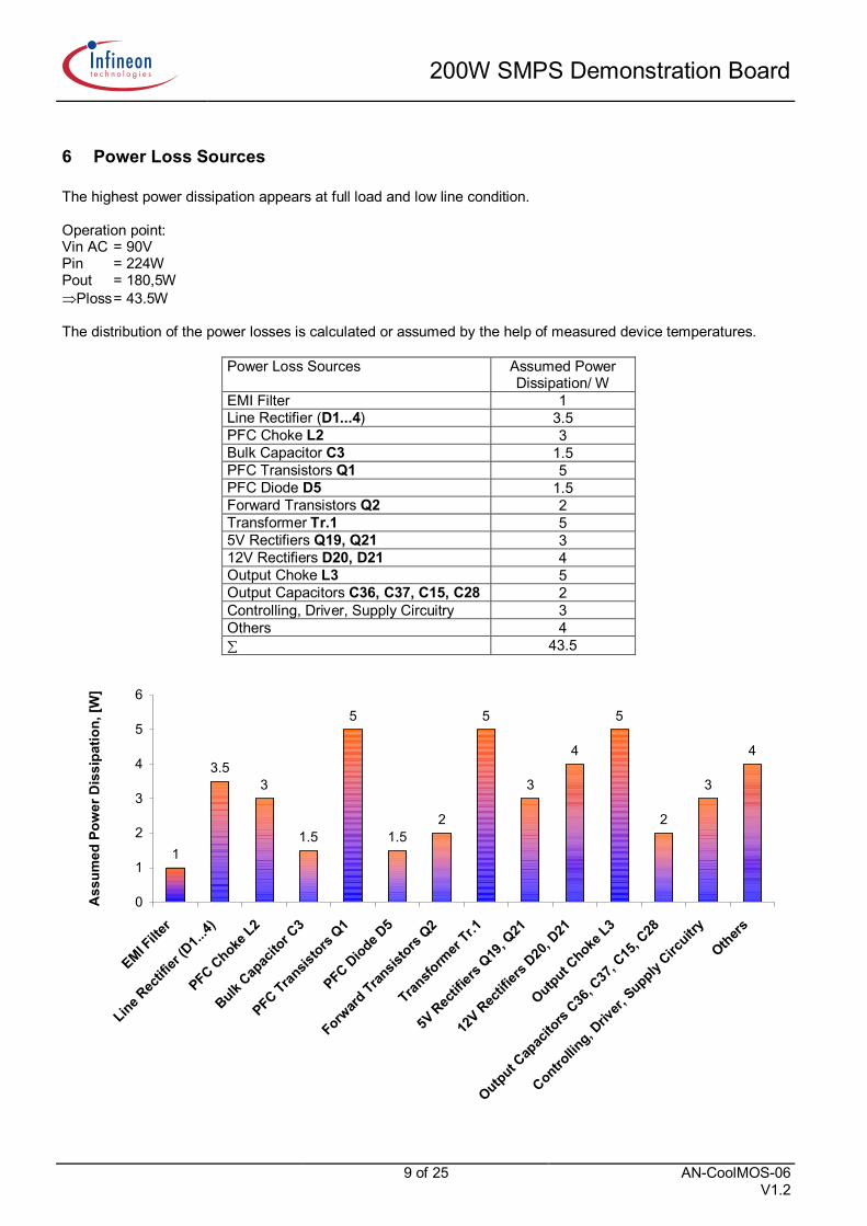
6 Power Loss Sources
The highest power dissipation appears at full load and low line condition.
Operation point:Vin AC = 90VPin = 224WPout = 180,5W�Ploss= 43.5W
The distribution of the power losses is calculated or assumed by the help of measured device temperatures.
Power Loss Sources Assumed PowerDissipation/ W
EMI Filter 1Line Rectifier (D1...4) 3.5PFC Choke L2 3Bulk Capacitor C3 1.5PFC Transistors Q1 5PFC Diode D5 1.5Forward Transistors Q2 2Transformer Tr.1 55V Rectifiers Q19, Q21 312V Rectifiers D20, D21 4Output Choke L3 5Output Capacitors C36, C37, C15, C28 2Controlling, Driver, Supply Circuitry 3Others 4� 43.5
1
3.53
1.5
5
1.52
5
3
4
5
2
3
4
0
1
2
3
4
5
6
EMI Filte
r
Line Rec
tifier
(D1..
.4)
PFC Choke L2
Bulk Cap
acito
r C3
PFC Transis
tors Q1
PFC Diode D5
Forward
Transis
tors Q2
Transfo
rmer
Tr.1
5V Rec
tifiers
Q19
, Q21
12V Rec
tifiers
D20, D
21
Output Choke
L3
Output Cap
acito
rs C36
, C37
, C15
, C28
Controllin
g, Driv
er, Supply
Circuitry
Others
Ass
umed
Pow
er D
issi
patio
n, [W
]

200W SMPS Demonstration Board
10 of 25 AN-CoolMOS-06V1.2
7 Conducted EMI Measurements
Measuring of conducted noise with an EMI-Receiver FMLK 1518 at a Line-Impedance Stabilization Network(LISN) NSLK 8128.Conditions: VAC in = 230V, Pout = 181,4W, main board in a metal case.
Phase 1, Average
Phase 1, CISPR QP

200W SMPS Demonstration Board
11 of 25 AN-CoolMOS-06V1.2
Phase 2, Average
Phase 2, CISPR QP
As it can be seen from the figures above the measured EMI spectra are below the norm limit lines.

200W SMPS Demonstration Board
12 of 25 AN-CoolMOS-06V1.2
8 Construction of magnetic components
8.1 PFC choke
Core: MAGNETICS Ringcore 77930 - A7; L = 490 µH (Pin1 - Pin8)
N1: 56 turns 0,5mm �N2: 4 turns 0,2mm �N3: 4 turns 0,2mm �
Hole arrangementView in mounting direction
N3 N1 N2 Pin 1 2 43
Pin 8 7 6 5
N 1 N 2 N 3
200W SMPS Demonstration Board
13 of 25 AN-CoolMOS-06V1.2
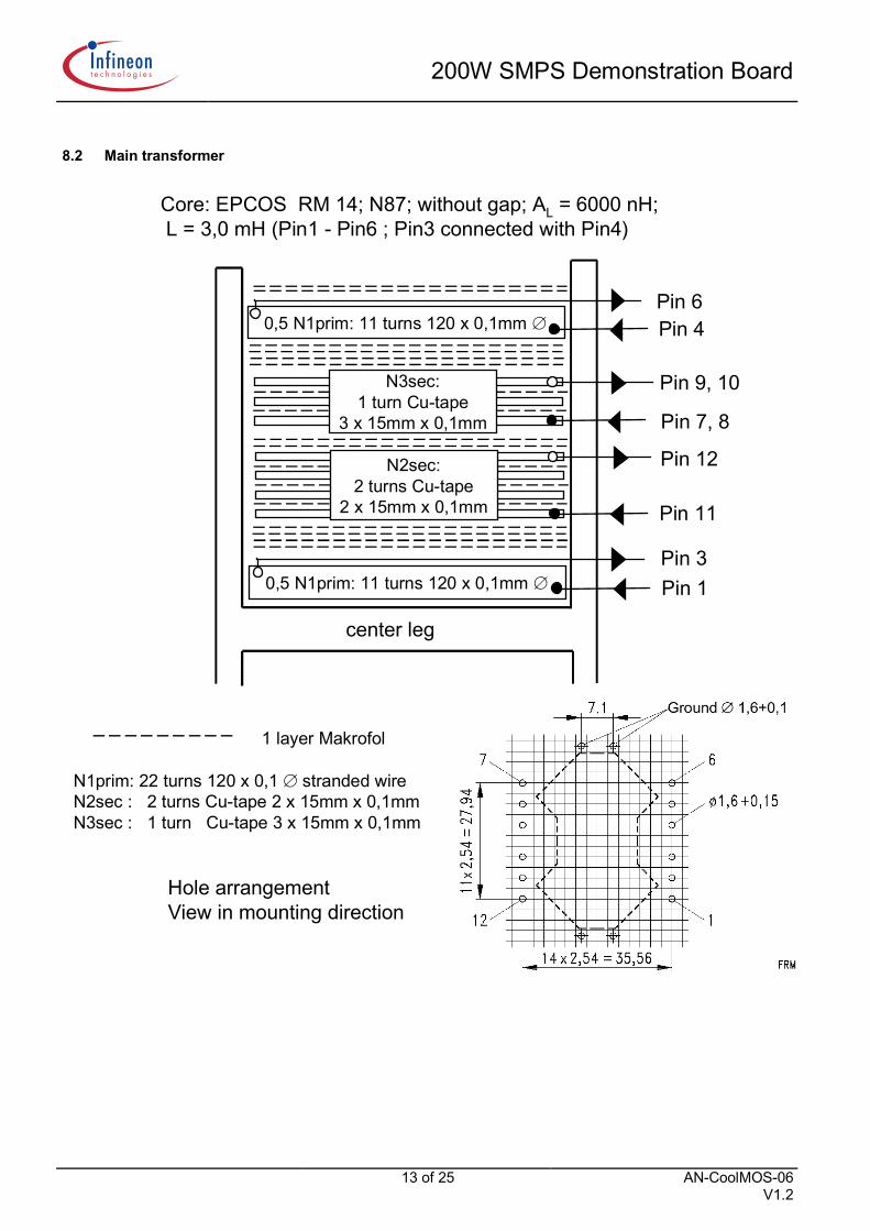
8.2 Main transformer
Core: EPCOS RM 14; N87; without gap; AL = 6000 nH; L = 3,0 mH (Pin1 - Pin6 ; Pin3 connected with Pin4)
N1prim: 22 turns 120 x 0,1 � stranded wireN2sec : 2 turns Cu-tape 2 x 15mm x 0,1mm N3sec : 1 turn Cu-tape 3 x 15mm x 0,1mm
1 layer Makrofol
Hole arrangementView in mounting direction
Pin 9, 10
center leg
Pin 12
Pin 3Pin 1
N2sec:2 turns Cu-tape
2 x 15mm x 0,1mm
N3sec:1 turn Cu-tape
3 x 15mm x 0,1mm
0,5 N1prim: 11 turns 120 x 0,1mm �
0,5 N1prim: 11 turns 120 x 0,1mm � Pin 4Pin 6
Pin 11
Pin 7, 8

200W SMPS Demonstration Board
14 of 25 AN-CoolMOS-06V1.2
8.3 Output filter choke
Core: EPCOS RM 14; N41; total gap = 1mm; AL = 250 nH; L = 36 µH (Pin1 - Pin6);(20A · 5turns + 10A · 12turns) · 250nH / 170mm² = 320mT
N1 : 5 turns Cu-tape 17mm x 0,1mm N2 : 12 turns Cu-tape 17mm x 0,1mm
1 layer Makrofol
Hole arrangementView in mounting direction
center leg
Pin 4, 5, 6
Pin 1, 2, 3Pin 7, 8, 9
Pin 10, 11, 12
N1:5 turns Cu-tape17mm x 0,1mm
N2:12 turns Cu-tape
2 x 17mm x 0,1mm
200W SMPS Demonstration Board
15 of 25 AN-CoolMOS-06V1.2
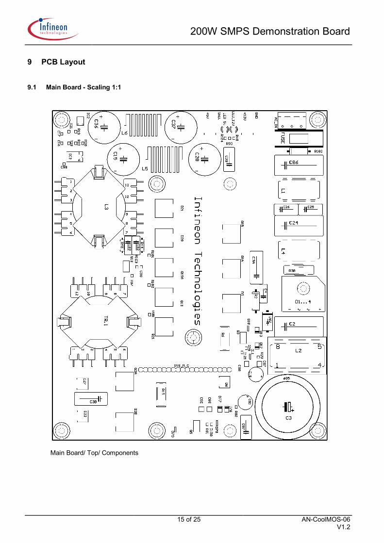
9 PCB Layout
9.1 Main Board - Scaling 1:1
Main Board/ Top/ Components

200W SMPS Demonstration Board
16 of 25 AN-CoolMOS-06V1.2
Main Board /Top / Copper
200W SMPS Demonstration Board
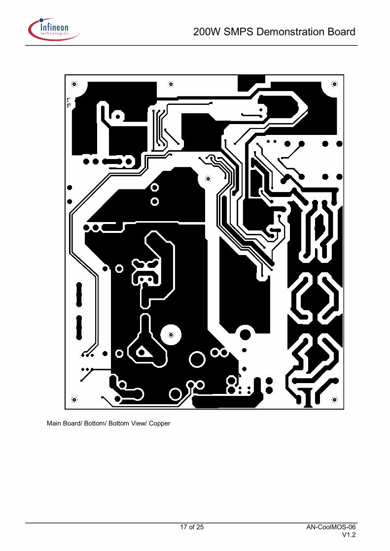
17 of 25 AN-CoolMOS-06V1.2
Main Board/ Bottom/ Bottom View/ Copper

200W SMPS Demonstration Board
18 of 25 AN-CoolMOS-06V1.2
9.2 Control Board- Scaling 1:1
Control Board/ Top/ Components
Control Board/ Top/ Copper
Control Board/ Bottom/ Bottom View/ Components Control Board/ Bottom/ Bottom View/ Copper
10 Bill of Materials
10.1 Main Board
Part Value Package Library Position (mil) Orientation
+5V FLSTL6,3 CON-RIB (500 3275) R180
+12V FLSTL6,3 CON-RIB (500 4075) R180
AC_IN KLEMME-3 WAGO508 (200 5150) R270
C2 u47/X2 C22,5B11 CAP-WI (4650 5300) R90
C3 150u/450V EB35D POLCAP (6375 5053.74) R270
C3A 100n/630V C15B7 CAP-WI (3375 4387.5) R180
C3B 100n/630V C15B7 CAP-WI (6200 825) R270
C4 2n2/1kV C7,5B4 CAP-WI (3937.5 4537.5) R180
C15 2m2/16V E3P-18 POLCAP (1050 1525) R90
C16 68n 1206 SMD (700 200) R0
C17 2n2 1206 SMD (500 200) R0
C18 47u/63V E3,5-8 POLCAP (5675 4375) R270
C24 u47/X2 C22,5B11 CAP-WI (2475 5300) R90
C25 4n7/Y C10B6 CAP-WI (2125 5550) R90
C26 4n7/Y C10B6 CAP-WI (2125 5025) R90
C28 2m2/16V E3P-18 POLCAP (1050 3275) R90
C32 2n2/1kV C7,5B4 CAP-WI (2900 1800) R0
C33 2n2/1kV C7,5B4 CAP-WI (2900 1625) R0
200W SMPS Demonstration Board
19 of 25 AN-CoolMOS-06V1.2
Part Value Package Library Position (mil) Orientation
C36 1m/25V E3P-18 POLCAP (362.5 1112.5) R90
C37 1m/25V E3P-18 POLCAP (362.5 2762.5) R90
C39 4n7/Y C10B6 CAP-WI (1050 3800) R180
C86 u47/X2 C22,5B11 CAP-WI (1175 5300) R90
C87 u47 1812 SMD (5450 4450) R270
C88 u47 1812 SMD (5450 4175) R90
C89 u47 1812 SMD (6425 3375) R0
C90 u47 1812 SMD (6425 3200) R0
C91 47u/63V E3,5-8 POLCAP (6275 4150) R0
C97 4n7/Y C10B6 CAP-WI (6812.5 4162.5) R180
C98 4n7 1206 SMD (3362.5 1912.5) R180
C99 2n2 1206 SMD (1143.75 250) R90
C100 100n 1206 SMD (6750 3418.75) R180
C101 100n 1206 SMD (5200 4075) R0
D1...4 KBU8K KBU-L RECTIF (4375 5400) R270
D5 SDB06S60 D2PAK SMD-SPC (4150 3925) R180
D6 SDD04E60 DPAK SMD-SPC (5837.5 3700) R180
D10 BAV99 SOT-23 SMD (4681.25 4206.25) R0
D11 BZX84C13 SOT-23 SMD (5287.5 4250) R0
D12 TMBYV10-60 MELF SMD (5062.5 4400) R180
D13 TMBYV10-60 MELF SMD (4725 4400) R180
D20 MBRB2545 D2PAK SMD-SPC (2737.5 2325) R0
D21 MBRB2545 D2PAK SMD-SPC (2100 2325) R0
D22 SDD04E60 DPAK SMD-SPC (6575 650) R180
D27 SDD04E60 DPAK SMD-SPC (5875 642.52) R180
D76 TMBYV10-60 MELF SMD (6425 3750) R0
D77 TMBYV10-60 MELF SMD (6425 3600) R0
D78 BZX84C13 SOT-23 SMD (6725 3537.5) R180
D79 BAV99 SOT-23 SMD (6862.5 2637.5) R0
D82 1N5408 DO201-15 DIODE (4531.25 4625) R0
E$5 BO3,2-P HOLES (6889.76 3818.9) R0
E$9 BO3,2-P HOLES (1574.8 3818.9) R0
FUSE 4AT SH22 FUSE (600 5300) R90
GND FLSTL6,3 CON-RIB (500 4325) R180
GND. FLSTL6,3 CON-RIB (500 3525) R180
IC2 TL431CD SO-8 SMD-IC (250 600) R180
IC3 CNY17-3 DIL06 OPTOCPL (987.5 475) R270
L1 2x1m2 82722J IND-A (1700 5300) R90
L2 500u INF-PFC IND-A (5275 5262.5) R90
L3 36/6uH RM14-12A IND-B (2075 1000) R270
L4 2x1m2 82722J IND-A (3000 5300) R90
L5 1u INAIR20A IND-A (1050 2400) R90
L6 1u INAIR8A IND-A (312.5 1937.5) R90
200W SMPS Demonstration Board
20 of 25 AN-CoolMOS-06V1.2
Part Value Package Library Position (mil) Orientation
LED_5V Green/LC LED3 LED (400 3706.25) R180
LED_12V Red LED3 LED (400 3893.75) R180
Q1A SPB11N60C2 D2PAK SMD-SPC (3400 3925) R180
Q1B SPB11N60C2 D2PAK SMD-SPC (2650 3925) R180
Q2A SPB11N60C2 D2PAK SMD-SPC (5862.5 1625) R180
Q2B SPB11N60C2 D2PAK SMD-SPC (6700 1625) R180
Q3 BSP129 SOT-223 SMD (4887.5 4100) R180
Q5 BSP129 SOT-223 SMD (6787.5 3100) R180
Q18 BSP318 SOT-223 SMD (3350 1587.5) R0
Q19 SPB80N03S2L-03 D2PAK SMD-SPC (4012.5 2325) R0
Q19A SPB80N03S2L-03 D2PAK SMD-SPC (3375 2325) R0
Q21 SPB80N03S2L-03 D2PAK SMD-SPC (4650 2325) R0
R2 220k/2W 0411/15 R (4100 4375) R180
R6 0R15/1W R-SMR SMD-SPC (4900 3700) R180
R15 R47 R-SMR SMD-SPC (6112.5 2337.5) R0
R19 5k1 1206 SMD (450 500) R180
R20 5k1 1206 SMD (700 650) R180
R21 10k 1206 SMD (450 350) R180
R22 680R 1206 SMD (700 500) R180
R28 4k7 1206 SMD (5112.5 4168.75) R0
R29 1R 1206 SMD (5300 4425) R90
R30 S14K275 S14K275 VARIST (3425 5300) R0
R39 1k 1206 SMD (700 350) R0
R44 4R7/0,6W 0207/10 R (2900 1925) R0
R45 4R7/0,6W 0207/10 R (2900 1500) R0
R48 1k8 1206 SMD (593.7 3897.98) R0
R80 1R 1206 SMD (6375 3950) R0
R81 4k7 1206 SMD (6750 3325) R0
R97 10R 1206 SMD (3550 1712.5) R180
R98 1R 1206 SMD (4387.5 2087.5) R0
R99 1k8 1206 SMD (593.75 3806.25) R0
R100 1R 1206 SMD (3750 2075) R0
R101 1R 1206 SMD (3112.5 2075) R0
R102 1M2/Netz 0411/15 R (875 5300) R90
R103 47R 1206 SMD (3362.5 1812.5) R0
R104 1k8 1206 SMD (593.75 3712.5) R0
S$63 BO3,2-P HOLES (3825 5400) R0
SVB_M_C 1X20SMDI PINHEAD (5575 2850) R270
TR.1 RM14-12A IND-B (4550 1000) R0

200W SMPS Demonstration Board
21 of 25 AN-CoolMOS-06V1.2
10.2 Control Board
Part Value Package Library Position (mil) Orientation
C5 47n 1206 SMD (900 968.75) R270
C6 100n 1206 SMD (818.75 968.75) R90
C7 220p 1206 SMD (1699.36 1050) MR0
C8 2n2 1206 SMD (1699.36 968.75) MR180
C9A 2n2 1206 SMD (1699.36 1131.26) MR180
C10 47p 1206 SMD (1424.36 906.24) R0
C11 u47 1812 SMD (1511.85 528.12) MR180
C11A 220u/25V E3,5-8 POLCAP (150 1025) R0
C12 u47 1812 SMD (1561.87 1103.13) R0
C13 47p 1206 SMD (1424.37 825) R180
C14 u47 1812 SMD (1252.48 528.12) MR180
C21 100p 1206 SMD (1424.37 656.25) R180
C22 4n7 1206 SMD (1424.37 743.75) R180
C41 220p 1206 SMD (1424.36 987.5) R180
C92 u47 1812 SMD (975 749.36) R90
C93 100p 1206 SMD (1653.13 756.25) MR90
C94 100n 1206 SMD (2018.75 537.5) MR90
C95 47u/63V E3,5-8 POLCAP (1965.63 993.75) R90
C96 u47 1812 SMD (2287.5 703.13) R90
D80 BAV99 SOT-23 SMD (1700 571.87) MR180
D81 BAV99 SOT-23 SMD (1678.12 734.37) R270
IC1 TDA16888 SO-20L SMD-IC (1380.61 918.75) MR270
IC7 HEF40106BT SO-14 SMD-IC (849.36 981.25) MR180
IC8 SFH6711 DIL-08 IC (1943.11 631.25) R270
IC9 HEF40106BT SO-14 SMD-IC (2175 988.14) MR270
Q6 BC817 SOT-23 SMD (618.75 884.38) MR0
Q7 BC807 SOT-23 SMD (487.5 884.38) MR0
Q8 BSP613P SOT-223 SMD (468.11 643.75) MR180
Q9 BSP320S SOT-223 SMD (199.36 643.75) MR180
Q10 BC817 SOT-23 SMD (818.75 687.5) R0
Q11 BC807 SOT-23 SMD (818.76 815.63) R180
Q12 BSP613P SOT-223 SMD (736.86 643.75) MR180
Q13 BSP320S SOT-223 SMD (1005.61 643.75) MR180
Q14 BC817 SOT-23 SMD (2275.01 659.37) MR180
Q15 BC807 SOT-23 SMD (2275 471.88) MR180
Q16 BSP613P SOT-223 SMD (1961.86 181.25) MR180
Q17 BSP320S SOT-223 SMD (2224.35 181.25) MR180
R1A 1M 1206 SMD (568.11 550) R90
R1B 1M 1206 SMD (568.11 725) R90
R1C 1M 1206 SMD (568.11 900) R90
R1D 820k 1206 SMD (568.11 1075) R90

200W SMPS Demonstration Board
22 of 25 AN-CoolMOS-06V1.2
Part Value Package Library Position (mil) Orientation
R3 10k 1206 SMD (1549.36 478.13) R0
R4A 470k 1206 SMD (180.61 550) R90
R4B 470k 1206 SMD (180.61 725) R90
R5 1k8 1206 SMD (1374.36 478.13) R180
R7 1k8 1206 SMD (1233.74 587.5) R0
R8 10k 1206 SMD (1699.36 887.5) MR0
R11 51k 1206 SMD (443.75 1087.5) MR90
R12A 1M 1206 SMD (443.11 550) R90
R12B 1M 1206 SMD (443.11 725) R90
R12C 1M 1206 SMD (443.11 900) R90
R12D 820k 1206 SMD (443.11 1075) R90
R13A 1M 1206 SMD (343.11 550) R90
R13B 1M 1206 SMD (343.11 725) R90
R13C 1M 1206 SMD (343.11 900) R90
R13D 820k 1206 SMD (343.11 1075) R90
R14 51k 1206 SMD (318.75 1087.5) MR90
R16 390k 1206 SMD (981.26 968.75) R270
R23 33k 1206 SMD (1556.25 312.5) MR0
R24 22k 1206 SMD (1118.75 950) MR270
R25 10k 1206 SMD (1121.87 950) R270
R26 33k 1206 SMD (1714.98 987.5) R90
R27 51k 1206 SMD (568.76 1087.5) MR90
R32 1k 1206 SMD (1150 312.5) MR0
R35 1k 1206 SMD (1121.87 775) R90
R82 10R 1206 SMD (1043.75 531.26) R90
R83 4R7 1206 SMD (256.25 940.63) MR0
R84 22R 1206 SMD (700 187.5) MR270
R85 4R7 1206 SMD (787.5 187.5) MR270
R86 22R 1206 SMD (956.25 187.5) MR270
R87 4R7 1206 SMD (868.75 187.5) MR270
R88 4R7 1206 SMD (718.75 706.25) R270
R89 22R 1206 SMD (878.13 531.25) R90
R90 4R7 1206 SMD (962.5 531.25) R90
R91 1k 1206 SMD (1700.01 584.38) R90
R92 1k 1206 SMD (1718.76 756.25) MR90
R93 10R 1206 SMD (2168.75 687.5) MR90
R94 4R7 1206 SMD (2293.75 459.38) R90
R95 22R 1206 SMD (1781.25 100) MR90
R96 4R7 1206 SMD (1700 100) MR90
SVB_C_M 1X20/90I PINHEAD (1205.61 400) R0

200W SMPS Demonstration Board
23 of 25 AN-CoolMOS-06V1.2
This demonstration board was designed by
ISLEISLE GmbHEhrenbergstr. 3398693 IlmenauGermany
Revision HistoryApplication Note AN-CoolMOS-06Actual Release: V1.2 Date:2001-11-14 Previous Release: V1.1Page ofactualRelease
Page ofprev.Release
Subjects changed since last release
Construction of magnetic components added.

200W SMPS Demonstration Board
24 of 25 AN-CoolMOS-06V1.2
For questions on technology, delivery and prices please contact the Infineon TechnologiesOffices in Germany or the Infineon Technologies Companies and Representatives worldwide:see the address list on the last page or our webpage at
http://www.infineon.com
CoolMOS� and CoolSET� are trademarks of Infineon Technologies AG.Edition 2000-03-03����������� �� �� ���� ����������
��������� �����������
�� !�"!�# ���
�� �� �� ���� ���������$%%%�
���&�����&����'��
���� ��� (�����)
��������������������� ������������ �������������������� ����� ��������������� ������� ����������������� ��� �
�� �������������������� ���������������������� �����
����������� ������������������������ ������������������������������������� ���������������������������������� ���� ������� ��������� � ������������
�������������������� �� ���������������������������
� ���*����
�������������������������������������������� �������������� ��������� ����� ������������������ ���������������������� � ���������!���������
�������������������� �"��� �������� ����������# ������� ��� �$�
+�� � ��
%�����������������&������ ��������� ������������������� � �� ����� �������������������������� ����&�� ��������� ������������������ ����������
����������� � ������
�������������������� ��������� ������������� ����������� ������������ ��� � �� �����������'�� ��������������������������������������� ����������������
������������ ������� �����������'������������� �������������������������� ��������������� � �������������������� ������������������� �����������������
� ����(���� ������������ ��� � �� ��������������������������������������������������� ���������)�������������� � ��������)����������������������
��������������� ��� ����������� ��������������������������� ����������� �� �����������������

200W SMPS Demonstration Board
25 of 25 AN-CoolMOS-06V1.2
������������������ ���� ��� ������ �����������
������������ ��������������� ���
ASiemens AG ÖsterreichErdberger Lände 26A-1031 WienT (+43)1-17 07-3 56 11Fax (+43)1-17 07-5 59 73AUSSiemens Ltd.885 Mountain HighwayBayswater,Victoria 3153T (+61)3-97 21 21 11Fax (+61)3-97 21 72 75BSiemens Electronic ComponentsBeneluxCharleroisesteenweg 116/Chaussée de Charleroi 116B-1060 Brussel/BruxellesT (+32)2-5 36 69 05Fax (+32)2-5 36 28 57Email:[email protected] Ltda.SemiconductoresAvenida Mutinga,3800-Pirituba05110-901 São Paulo-SPT (+55)11-39 08 25 64Fax (+55)11-39 08 27 28CDNInfineon Technologies Corporation320 March Road,Suite 604Canada,Ontario K2K 2E2T (+1)6 13-5 91 63 86Fax (+1)6 13-5 91 63 89CHSiemens Schweiz AGBauelementeFreilagerstrasse 40CH-8047 ZürichT (+41)1-4 953065Fax (+41)1-4 955050DInfineon Technologies AGVölklinger Str.2D-40219 DüsseldorfT (+49)2 11-3 99 29 30Fax (+49)2 11-3 99 14 81Infineon Technologies AGWerner-von-Siemens-Platz 1D-30880 Laatzen (Hannover)T (+49)5 11-8 77 22 22Fax (+49)5 11-8 77 15 20Infineon Technologies AGVon-der-Tann-Straße 30D-90439 NürnbergT (+49)9 11-6 54 76 99Fax (+49)9 11-6 54 76 24Infineon Technologies AGWeissacher Straße 11D-70499 StuttgartT (+49)7 11-1 37 33 14Fax (+49)7 11-1 37 24 48DInfineon Technologies AGHalbleiter DistributionRichard-Strauss-Straße 76D-81679 MünchenT (+49)89-92 21 40 86Fax (+49)89-92 21 20 71DKSiemens A/SBorupvang 3DK-2750 BallerupT (+45)44 77-44 77Fax (+45)44 77-40 17ESiemens S.A.Dpto.ComponentesRonda de Europa,5E-28760 Tres Cantos-MadridT (+34)91-5 14 71 51Fax (+34)91-5 14 70 13
FInfineon Technologies France,39/47,Bd.OrnanoF-93527 Saint-Denis CEDEX2T (+33)1-49 22 31 00Fax (+33)1-49 22 28 01FINSiemens ComponentsScandinaviaP.O .Bo x 6 0FIN-02601 Espoo (Helsinki)T (+3 58)10-5 11 51 51Fax (+3 58)10-5 11 24 95Email:[email protected] TechnologiesSiemens HouseOldburyGB-Bracknell,BerkshireRG12 8FZT (+44)13 44-39 66 18Fax (+44)13 44-39 66 32HSimacomp Kft.Lajos u.103H-1036 BudapestT (+36)1-4 57 16 90Fax (+36)1-4 57 16 92HKInfineon TechnologiesHong Kong Ltd.Suite 302,Level 3,Festival Walk,80 Tat Chee Avenue,Yam Yat Tsuen,Kowloon TongHong KongT (+8 52)28 32 05 00Fax (+8 52)28 27 97 62ISiemens S..A.Semiconductor SalesVia Piero e Alberto Pirelli,10I-20126 MilanoT (+39)02-66 76 -1Fax (+39)02-66 76 43 95INDSiemens Ltd.Components DivisionNo.84 Keonics Electronic CityHosur RoadBangalore 561 229T (+91)80-8 52 11 22Fax (+91)80-8 52 11 80Siemens Ltd.CMP Div,5th Floor4A Ring Road,IP EstateNew Delhi 110 002T (+91)11-3 31 99 12Fax (+91)11-3 31 96 04Siemens Ltd.CMP Div,4th Floor130,Pandurang Budhkar Marg,WorliMumbai 400 018T (+91)22-4 96 21 99Fax (+91)22-4 96 22 01IRLSiemens Ltd.Electronic Components Division8,Raglan RoadIRL-Dublin 4T (+3 53)1-2 16 23 42Fax (+3 53)1-2 16 23 49ILNisko Ltd.2A,Habarzel St.P.O.Box 5815161580 Tel Aviv –IsrealT (+9 72)3 -7 65 73 00Fax (+9 72)3 -7 65 73 33
JSiemens Components K.K.Talanawa Park Tower 12F &17F3-20-14,Higashi-Gotanda,Shinagawa-kuTokyoT (+81)3-54 49 64 11Fax (+81)3 -54 49 64 01MALInfineon Technologies AGSdn BhdBayan Lepas Free Industrial Zone111900 PenangT (+60)4 -6 44 99 75Fax (+60)4 -6 41 48 72NSiemens ComponentsScandinaviaØstre Aker vei 24Postboks 10,VeitvetN-0518 OsloT (+47)22-63 30 00Fax (+47)22-68 49 13Email:[email protected] Electronic ComponentsBeneluxPostbus 16068NL-2500 BB Den HaagT (+31)70-3 33 20 65Fax (+31)70-3 33 28 15Email:[email protected] Auckland300 Great South RoadGreenlandAucklandT (+64)9-5 20 30 33Fax (+64)9-5 20 15 56PSiemens S.A.an Componentes ElectronicosR.Irmaos Siemens,1AlfragideP-2720-093 AmadoraT (+351)1-4 17 85 90Fax (+351)1-4 17 80 83PKSiemens Pakistan EngineeringCo.Ltd.PO Box 1129,Islamabad 4400023 West Jinnah AveIslamabadT (+92)51-21 22 00Fax (+92)51-21 16 10PLSiemens SP.z.o.o.ul.Zupnicza 11PL-03-821 WarszawaT (+48)22-8 70 91 50Fax (+48)22-8 70 91 59ROKSiemens Ltd.Asia Tower,10th Floor726 Yeoksam-dong,Kang-nam KuCPO Box 3001Seoul 135-080T (+82)2-5 27 77 00Fax (+82)2-5 27 77 79RUSINTECH electronicsul.Smolnaya,24/1203RUS-125 445 MoskvaT (+7)0 95 -4 51 97 37Fax (+7)0 95 -4 51 86 08SSiemens Components ScandinaviaÖsterögatan 1,Box 46S-164 93 KistaT (+46)8-7 03 35 00Fax (+46)8-7 03 35 01Email:[email protected]
RCInfineon TechnologiesAsia Pacific Pte.Ltd.Taiwan Branch10F,No.136 Nan King East RoadSection 23,TaipeiT (+8 86)2-27 73 66 06Fax (+8 86)2-27 71 20 76SGPInfineon Technologies AsiaPacific,Pte.Ltd.168 Kallang WaySingapore 349 253T (+65)8 40 06 10Fax (+65)7 42 62 39USAInfineon Technologies Corporation1730 North First StreetSan Jose,CA 95112T (+1)4 08-5 01 60 00Fax (+1)4 08-5 01 24 24Siemens Components,Inc.Optoelectronics Division19000 Homestead RoadCupertino,CA 95014T (+1)4 08-2 57 79 10Fax (+1)4 08-7 25 34 39Siemens Components,Inc.Special Products Division186 Wood Avenue SouthIselin,NJ 08830-2770T (+1)7 32-9 06 43 00Fax (+1)7 32-6 32 28 30VRCInfineon TechnologiesHong Kong Ltd.Beijing OfficeRoom 2106,Building AVantone New World PlazaNo.2 Fu Cheng Men Wai Da JieJie100037 BeijingT (+86)10 -68 57 90 -06,-07Fax (+86)10 -68 57 90 08Infineon TechnologiesHong Kong Ltd.Chengdu OfficeRoom14J1,Jinyang Mansion58 Tidu StreetChengdu,Sichuan Province 610 016T (+86)28-6 61 54 46 /79 51Fax (+86)28 -6 61 01 59Infineon TechnologiesHong Kong Ltd.Shanghai OfficeRoom1101,Lucky Target SquareNo.500 Chengdu Road NorthShanghai 200003T (+86)21-63 6126 18 /19Fax (+86)21-63 61 11 67Infineon TechnologiesHong Kong Ltd.Shenzhen OfficeRoom 1502,Block ATian An International BuildingRenim South RoadShenzhen 518 005T (+86)7 55 -2 28 91 04Fax (+86)7 55-2 28 02 17ZASiemens Ltd.Components DivisionP.O.B.3438Halfway House 1685T (+27)11-6 52 -27 02Fax (+27)11-6 52 20 42