Embed Size (px)
Citation preview
Pacific MicroCHIP Corp.
AN ASIC WITH A LOW POWER
MULTICHANNEL ADC FOR ENERGY
AND TIMING MEASUREMENTS
Anton Karnitski
Dalius Baranauskas
Award Number: DE-SC0018566
1
Pacific MicroCHIP Corp.
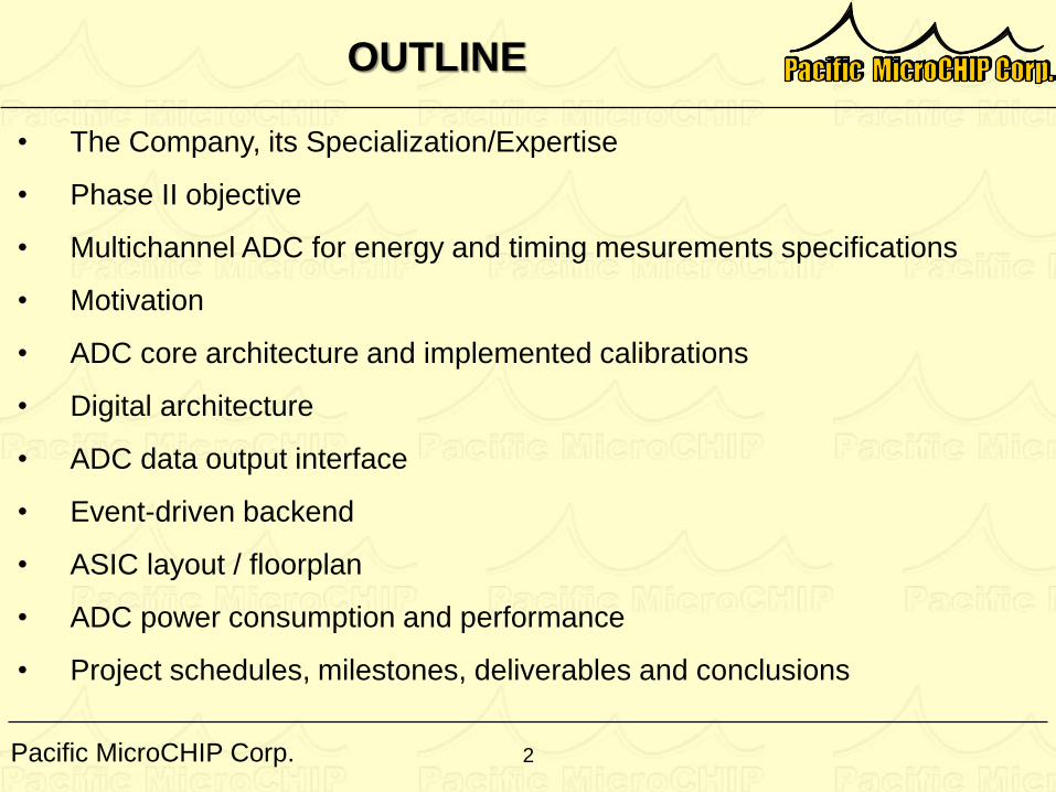
OUTLINE
• The Company, its Specialization/Expertise
• Phase II objective
• Multichannel ADC for energy and timing mesurements specifications
• Motivation
• ADC core architecture and implemented calibrations
• Digital architecture
• ADC data output interface
• Event-driven backend
• ASIC layout / floorplan
• ADC power consumption and performance
• Project schedules, milestones, deliverables and conclusions
2
Pacific MicroCHIP Corp.
COMPANY
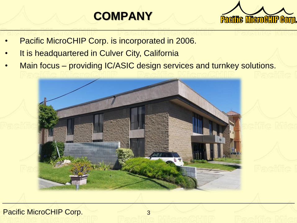
• Pacific MicroCHIP Corp. is incorporated in 2006.
• It is headquartered in Culver City, California
• Main focus – providing IC/ASIC design services and turnkey solutions.
3
Pacific MicroCHIP Corp.
CORE EXPERTISE
• Analog (ADC/DAC, CTF, VGA, BG, LDO)
• Mixed Signal (PLL, CDR, SerDes, MDrv, TIA)
• RF (LNA, Mixer/Modulator, PA)
• Digital (RTL, Synthesis, P&R, Timing Closure, DFT, Verifications)
• Layout (SiGe/CMOS) down to 7nm
4
Pacific MicroCHIP Corp.
PHASE II OBJECTIVE
5
• To design circuits and layout for the ADC ASIC.
• To fabricate the chip.
• To package the chips.
• To develop the test PCB and socket for the ASIC.
• To develop a GUI and a testbench.
• To test and characterize the ADC ASIC.
• To prepare a datasheet for marketing.
• To submit deliverables to the DoE.
Pacific MicroCHIP Corp.
ASIC SPECIFICATION
SER 10:1
SER 16:1
MUX CML
CML
[3.2/6.4]
Gbit/s
in_p
in_n
Direct DATA output
JESD204B output
3.2GHz
100Ω Diff
10b
Clock tree[3.2/0.2]GHz
. . .
clk[0] . . .
... ...
clk[31]
Frame
assembly
JESD204B
SER 32:8
8b/10b
FIFO
32x
32x
32x Data
12-bit32xClk
0.2GHz
FIFO
Calibration
CPU
ADC BIAS
Up to
100MHz
100Ω Diff
32Ch 12-bit 200MS/s ADC Array ASIC
I2C InterfaceRegister map
32x Data
12b
32xClk
0.2GHz
32xDigital back-end
DATA
50 Mbit/s
CLK
50MHz
32x
….
….
….
….
32x
Buffer
CLK 3.2GHz
Clk gen12b
200 MS/s
ADC channel [0]
data/
clk
synch4b+12b data
12b
16b
clk
48b
time
stamp
FIFO
and
Digital
Trigger
FIFO
and
Digital
Trigger
FIFO
and
Digital
Trigger
Event
builderEvent
builderEvent
builder
Shared
FIFO
Event
Memory
TX
UART
200MHzBuffer
MUX
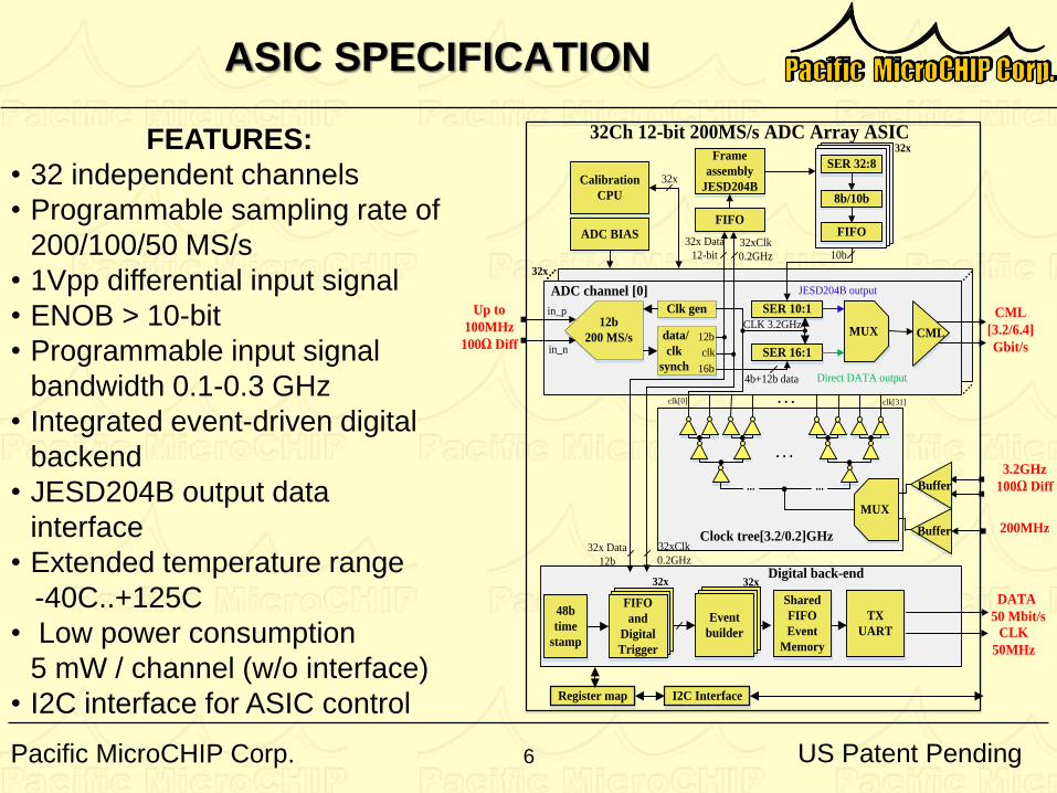
FEATURES:
• 32 independent channels
• Programmable sampling rate of
200/100/50 MS/s
• 1Vpp differential input signal
• ENOB > 10-bit
• Programmable input signal
bandwidth 0.1-0.3 GHz
• Integrated event-driven digital
backend
• JESD204B output data
interface
• Extended temperature range
-40C..+125C
• Low power consumption
5 mW / channel (w/o interface)
• I2C interface for ASIC control
US Patent Pending6
Pacific MicroCHIP Corp.
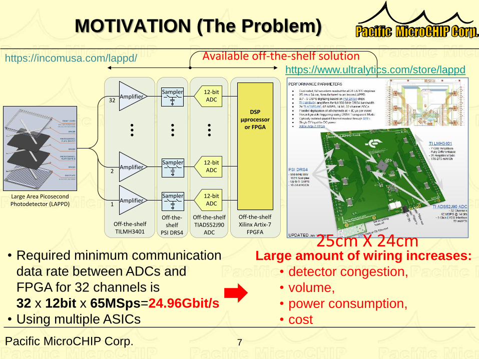
MOTIVATION (The Problem)
Large Area Picosecond Photodetector (LAPPD)
Amplifier
Amplifier
Amplifier
Off-the-shelfTILMH3401
1
2
32
12-bit ADC
12-bit ADC
12-bit ADC
Off-the-shelfTIADS52J90
ADC
DSPµprocessor
or FPGA
Off-the-shelfXilinx Artix-7
FPGFA
Sampler
Sampler
Sampler
Off-the-shelf
PSI DRS4
25cm X 24cm
Available off-the-shelf solution
• Required minimum communication
data rate between ADCs and
FPGA for 32 channels is
32 x 12bit x 65MSps=24.96Gbit/s
• Using multiple ASICs
Large amount of wiring increases:
• detector congestion,
• volume,
• power consumption,
• cost
https://www.ultralytics.com/store/lappdhttps://incomusa.com/lappd/
7
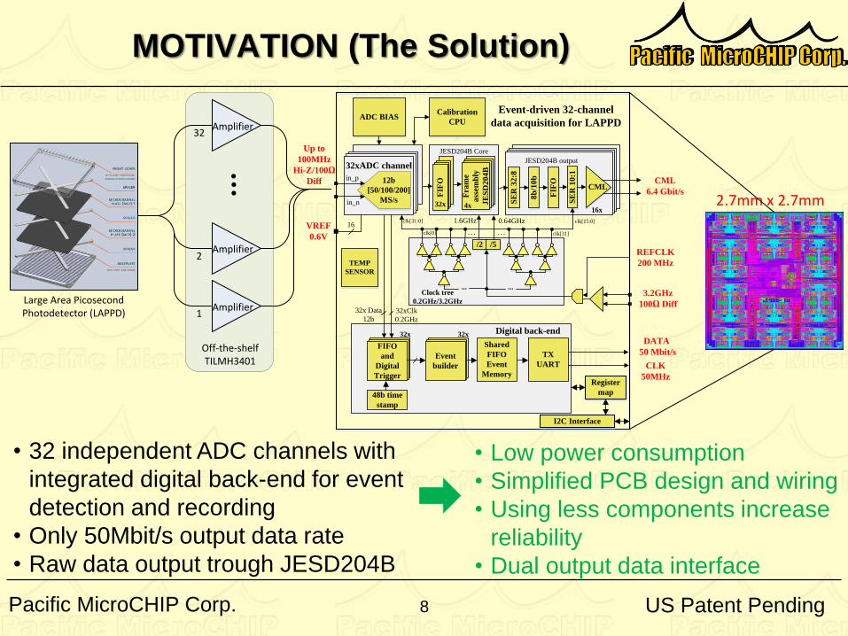
Pacific MicroCHIP Corp.
MOTIVATION (The Solution)
3.2GHz
100Ω Diff
Clock tree
0.2GHz/3.2GHz
. . .clk[0]
... ...
clk[31]
Calibration
CPUADC BIAS
Event-driven 32-channel
data acquisition for LAPPD
I2C Interface
Register
map
32x Data
12b
32xClk
0.2GHz
FIFO and Digital Trigger
FIFO and Digital Trigger
FIFO
and
Digital
Trigger
32x Digital back-end
FIFO and Digital Trigger
FIFO and Digital Trigger
Event
builder
Shared
FIFO
Event
Memory
TX
UART
DATA
50 Mbit/s
CLK
50MHz
48b time
stamp
32x
1.6GHz
0.64GHz
12b
[50/100/200]
MS/s
in_p
in_n
32xADC channel
Up to
100MHz
Hi-Z/100Ω
Diff
clk[31:0]
SE
R 1
0:1
CMLCML
6.4 Gbit/s
JESD204B output
16x
SE
R 3
2:8
8b
/10
b
FIF
O
FIF
OF
IFO
FIF
OF
IFO
32x
Fra
me
ass
emb
ly
JE
SD
20
4B
4x
JESD204B Core
clk[15:0]
/2 /5
. . .
TEMP
SENSOR
REFCLK
200 MHz
VREF
0.6V
16
Large Area Picosecond Photodetector (LAPPD)
Amplifier
Amplifier
Amplifier
Off-the-shelfTILMH3401
1
2
32
2.7mm x 2.7mm
• 32 independent ADC channels with
integrated digital back-end for event
detection and recording
• Only 50Mbit/s output data rate
• Raw data output trough JESD204B
• Low power consumption
• Simplified PCB design and wiring
• Using less components increase
reliability
• Dual output data interface
US Patent Pending8
Pacific MicroCHIP Corp.
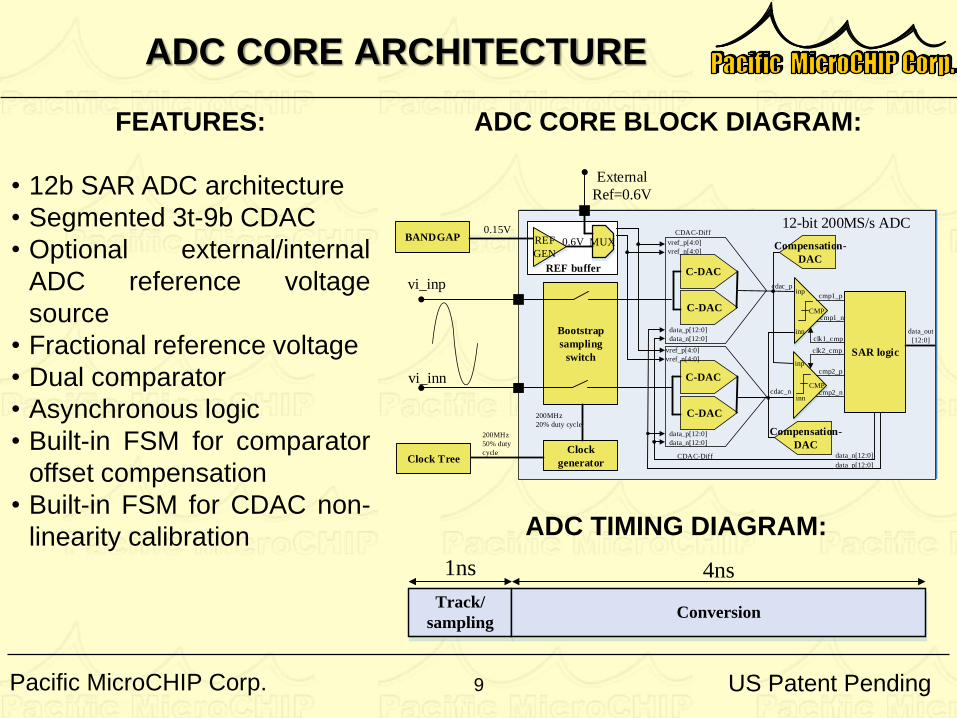
ADC CORE ARCHITECTURE
vi_inp
vi_inn
12-bit 200MS/s ADC
Clock
generator
Bootstrap
sampling
switch
200MHz
20% duty cycle
200MHz
50% duty
cycleClock Tree
C-DAC
C-DAC
C-DAC
C-DAC
CDAC-Diff
CDAC-Diff
SAR logic
data_n[12:0]
REF buffer
CMP
CMP
cmp1_p
cmp1_n
cmp2_p
cmp2_n
cdac_p
cdac_n
clk1_cmp
clk2_cmp
data_p[12:0]
data_n[12:0]
data_p[12:0]
data_n[12:0]
data_p[12:0]
External
Ref=0.6V
vref_p[4:0]
vref_n[4:0]
vref_p[4:0]
vref_n[4:0]
Compensation-
DAC
Compensation-
DAC
BANDGAP
inp
inn
inp
inn
REF
GENMUX0.6V
0.15V
data_out
[12:0]
1ns 4ns
Track/
samplingConversion
FEATURES:
• 12b SAR ADC architecture
• Segmented 3t-9b CDAC
• Optional external/internal
ADC reference voltage
source
• Fractional reference voltage
• Dual comparator
• Asynchronous logic
• Built-in FSM for comparator
offset compensation
• Built-in FSM for CDAC non-
linearity calibration
ADC CORE BLOCK DIAGRAM:
ADC TIMING DIAGRAM:
9 US Patent Pending
Pacific MicroCHIP Corp.
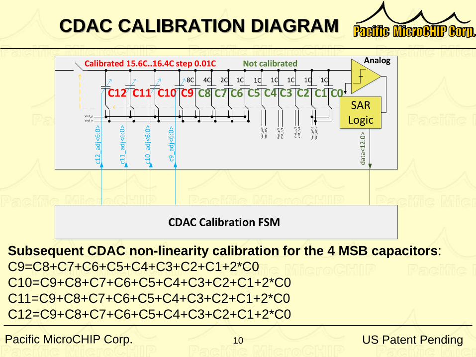
CDAC CALIBRATION DIAGRAM
c12
_ad
j<6
:0>
Vref_p
Vref_nc1
1_a
dj<
6:0
>
C12 C11
c10
_ad
j<6
:0>
C10
c9_a
dj<
6:0
>
C9 C88C
C74C
C62C
C51C
C41C
C31C
C21C
C11C
C01C
Vre
f_p
/2V
ref_
n/2
Vre
f_p
/4V
ref_
n/4
Vre
f_p
/8V
ref_
n/8
Vre
f_p
/16
Vre
f_n
/16
SAR Logic
Calibrated 15.6C..16.4C step 0.01C
dat
a<12
:0>
Analog
CDAC Calibration FSM
Not calibrated
Subsequent CDAC non-linearity calibration for the 4 MSB capacitors:
C9=C8+C7+C6+C5+C4+C3+C2+C1+2*C0
C10=C9+C8+C7+C6+C5+C4+C3+C2+C1+2*C0
C11=C9+C8+C7+C6+C5+C4+C3+C2+C1+2*C0
C12=C9+C8+C7+C6+C5+C4+C3+C2+C1+2*C0
10 US Patent Pending
Pacific MicroCHIP Corp.
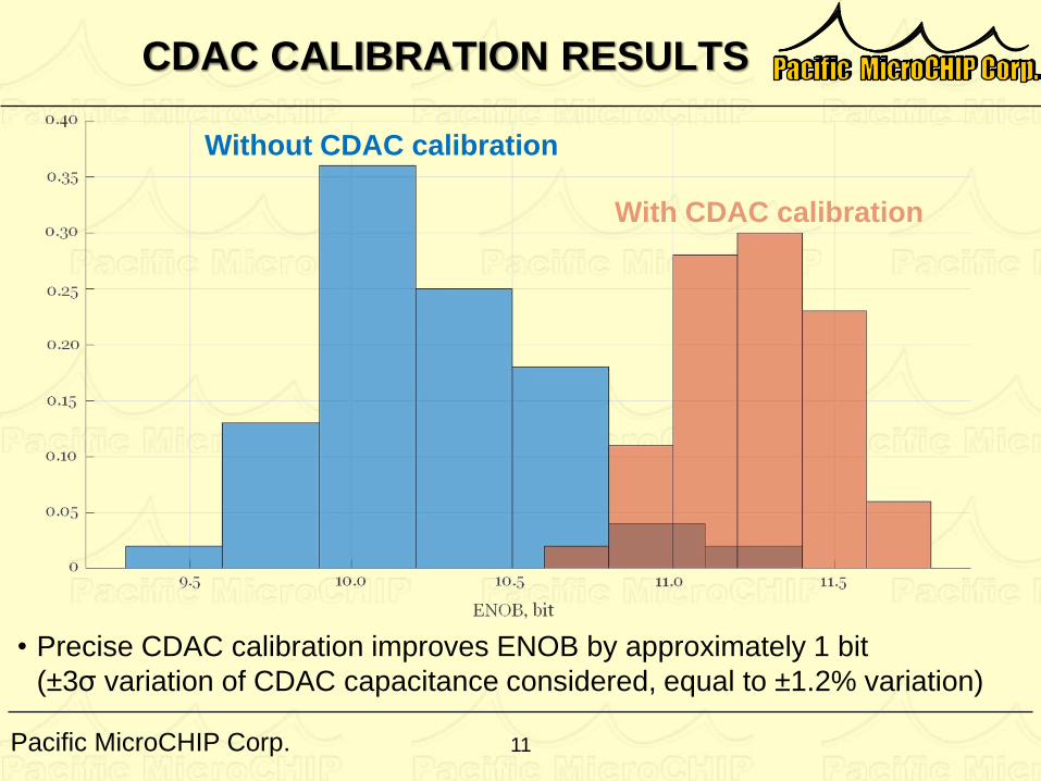
CDAC CALIBRATION RESULTS
• Precise CDAC calibration improves ENOB by approximately 1 bit
(±3σ variation of CDAC capacitance considered, equal to ±1.2% variation)
Without CDAC calibration
With CDAC calibration
11
Pacific MicroCHIP Corp.
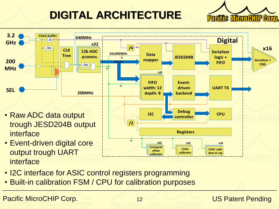
DIGITAL ARCHITECTURE
• Raw ADC data output
trough JESD204B output
interface
• Event-driven digital core
output trough UART
interface
Data mapper
JESD204B
CM
LC
ML
x16
FIFOwidth: 12depth: 8
FIFOwidth: 12depth: 8
FIFOwidth: 12depth: 8
x32
Event-driven
backendUART TX
Registers
Debug controller
I2C CPU
/4
32
32
640MHz
32x200MHz
200MHz
3.2 GHz
Serializer logic + FIFO
FIFOwidth: 12depth: 8
FIFOwidth: 12depth: 8
12b ADC@200MHz
x32/5
/16
200 MHz
Clock buffer
32x12b
Digital
Serializer +CML
CLK Tree
/16
32
SEL
/2
\CDAC calibrator
x32
\CDAC calib data to reg
x32
\Comparat
offset calibrator
x3232
• I2C interface for ASIC control registers programming
• Built-in calibration FSM / CPU for calibration purposes
12 US Patent Pending
Pacific MicroCHIP Corp.
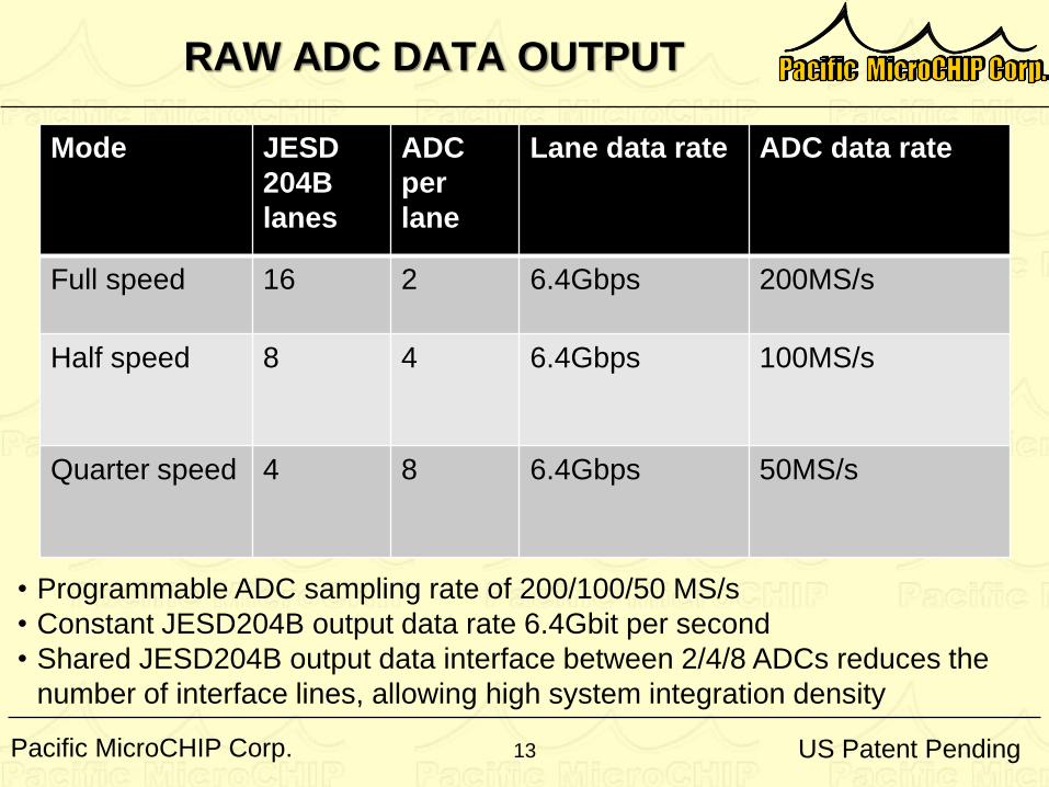
RAW ADC DATA OUTPUT
• Programmable ADC sampling rate of 200/100/50 MS/s
• Constant JESD204B output data rate 6.4Gbit per second
• Shared JESD204B output data interface between 2/4/8 ADCs reduces the
number of interface lines, allowing high system integration density
Mode JESD
204B
lanes
ADC
per
lane
Lane data rate ADC data rate
Full speed 16 2 6.4Gbps 200MS/s
Half speed 8 4 6.4Gbps 100MS/s
Quarter speed 4 8 6.4Gbps 50MS/s
13 US Patent Pending
Pacific MicroCHIP Corp.
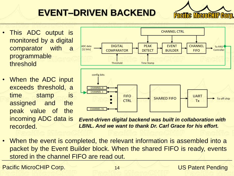
EVENT–DRIVEN BACKEND
SHARED FIFOUART
TxFIFOCTRL
To off chip
CHANNEL 0
CHANNEL 1
CHANNEL 31
config bits
DIGITAL COMPARATOR
PEAK DETECT
Threshold
ADC data[12 bits]
EVENT BUILDER
CHANNEL FIFO
Time Stamp
CHANNEL CTRL
To FIFO Controller
• This ADC output is
monitored by a digital
comparator with a
programmable
threshold
• When the ADC input
exceeds threshold, a
time stamp is
assigned and the
peak value of the
incoming ADC data is
recorded.
• When the event is completed, the relevant information is assembled into a
packet by the Event Builder block. When the shared FIFO is ready, events
stored in the channel FIFO are read out.
Event-driven digital backend was built in collaboration with
LBNL. And we want to thank Dr. Carl Grace for his effort.
14 US Patent Pending
Pacific MicroCHIP Corp.
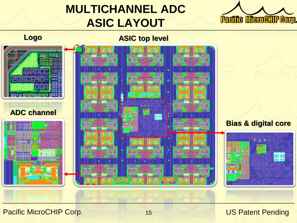
MULTICHANNEL ADC
ASIC LAYOUT
ASIC top levelLogo
ADC channel
Bias & digital core
15 US Patent Pending
Pacific MicroCHIP Corp.
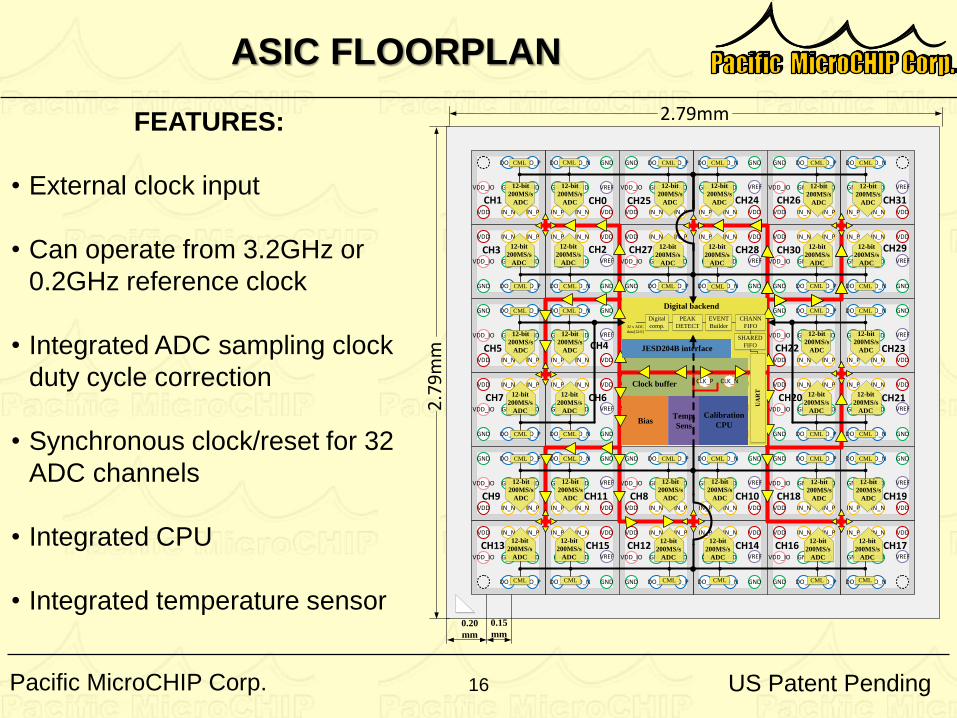
ASIC FLOORPLAN
FEATURES:
• External clock input
• Can operate from 3.2GHz or
0.2GHz reference clock
• Integrated ADC sampling clock
duty cycle correction
• Synchronous clock/reset for 32
ADC channels
• Integrated CPU
• Integrated temperature sensor0.15
mm
0.20
mm
CLK_NCLK_P
ADDR0
ADDR1 RST
TM
SESCL
TCK
SDA
SYNC
ADDR2REFCLK
P
REFCLKN
SYSREFP
SYSREFN
REXT
ATEST_P
ATEST_N GND
VDDGNDVDDPAD
VSSPAD
INTERFACE
GND
GND
GND
IN_NIN_P VDD
GND VREFGND
IN_N IN_P
DO_PDO_N
VDD
GNDVDD_IO GND
GND
IN_NIN_P
GNDGND
GND
IN_N IN_P
DO_PDO_N
GNDGND
VDDVDD
VDD_IO
DO_P DO_N
DO_P DO_N
CH1
CH3 CH2
GND
IN_NIN_P VDD
GND GND
IN_N IN_P
DO_PDO_N
VDD
GNDVDD_IO GND
GND
IN_NIN_P
GNDGND
GND
IN_N IN_P
DO_PDO_N
GNDGND
VDDVDD
VDD_IO
DO_P DO_N
DO_P DO_N
CH5
CH7
CH4
CH6
GND
GND
IN_NIN_P VDD
GND GND
IN_N IN_P
DO_PDO_N
VDD
GNDVDD_IO GND
GND
IN_NIN_P
GNDGND
GND
IN_N IN_P
DO_PDO_N
GNDGND
VDDVDD
VDD_IO
DO_P DO_N
DO_P DO_N
CH9
CH13
CH11
CH15
GND
IN_NIN_P VDD
GND GND
IN_N IN_P
DO_PDO_N
VDD
GNDVDD_IO GND
GND
IN_NIN_P
GNDGND
GND
IN_N IN_P
DO_PDO_N
GNDGND
VDDVDD
VDD_IO
DO_P DO_N
DO_P DO_N
CH25
CH27
CH24
CH28
GND
GND
IN_NIN_P VDD
GND GND
IN_N IN_P
DO_PDO_N
VDD
GNDVDD_IO GND
GND
IN_NIN_P
GNDGND
GND
IN_N IN_P
DO_PDO_N
GNDGND
VDDVDD
VDD_IO
DO_P DO_N
DO_P DO_N
CH8
CH12
CH10
CH14
GND
GND
IN_N IN_PVDD
GNDVDD_IO GND
IN_NIN_P
DO_P DO_N
VDD
GND GND
GND
IN_N IN_P
GND GND
GND
IN_NIN_P
DO_P DO_N
GND GND
VDD
VDD_IO
VDD
DO_PDO_N
DO_PDO_N
CH31
CH29
CH26
CH30
GND
IN_N IN_PVDD
GNDVDD_IO GND
IN_NIN_P
DO_P DO_N
VDD
GND GND
GND
IN_N IN_P
GND GND
GND
IN_NIN_P
DO_P DO_N
GND GND
VDD
VDD_IO
VDD
DO_PDO_N
DO_PDO_N
CH23
CH21
CH22
CH20
GND
GND
IN_N IN_PVDD
GNDVDD_IO GND
IN_NIN_P
DO_P DO_N
VDD
GND GND
GND
IN_N IN_P
GND GND
GND
IN_NIN_P
DO_P DO_N
GND GND
VDD
VDD_IO
VDD
DO_PDO_N
DO_PDO_N
CH19
CH17
CH18
CH16
GND GNDVDD_D
TX_DATA
TX_CLK
GND
VREF
VREF
VREF
VREF VREF
VREF
VREFVREF
VREF
VREF VREF VREF
VREF VREF VREF
VDD_D
VDD_D
VDD_D VDD_D
12-bit
200MS/s
ADC
12-bit
200MS/s
ADC
12-bit
200MS/s
ADC
12-bit
200MS/s
ADC
12-bit
200MS/s
ADC
12-bit
200MS/s
ADC
12-bit
200MS/s
ADC
12-bit
200MS/s
ADC
12-bit
200MS/s
ADC
12-bit
200MS/s
ADC
12-bit
200MS/s
ADC
12-bit
200MS/s
ADC
12-bit
200MS/s
ADC
12-bit
200MS/s
ADC
12-bit
200MS/s
ADC
12-bit
200MS/s
ADC
12-bit
200MS/s
ADC
12-bit
200MS/s
ADC
12-bit
200MS/s
ADC
12-bit
200MS/s
ADC
12-bit
200MS/s
ADC
12-bit
200MS/s
ADC
12-bit
200MS/s
ADC
12-bit
200MS/s
ADC
12-bit
200MS/s
ADC
12-bit
200MS/s
ADC
12-bit
200MS/s
ADC
12-bit
200MS/s
ADC
12-bit
200MS/s
ADC
12-bit
200MS/s
ADC
12-bit
200MS/s
ADC
12-bit
200MS/s
ADC
Temp.
SensBias
CLK_NCLK_P
CH0
2.79mm
2.7
9m
m
CML CML CML CML CML CML
CML CML
CML CML
CML CML CML CML CML CML
CML CML
CMLCML
CML CML CML CML CML CML
CML CML CML CML CML CML
Clock buffer
Digital backend
JESD204B interface
Calibration
CPU
32 x ADC
data[12:0]
PEAK
DETECT
EVENT
Builder
CHANN
FIFO
Digital
comp.
SHARED
FIFO
UA
RT
16 US Patent Pending
Pacific MicroCHIP Corp.
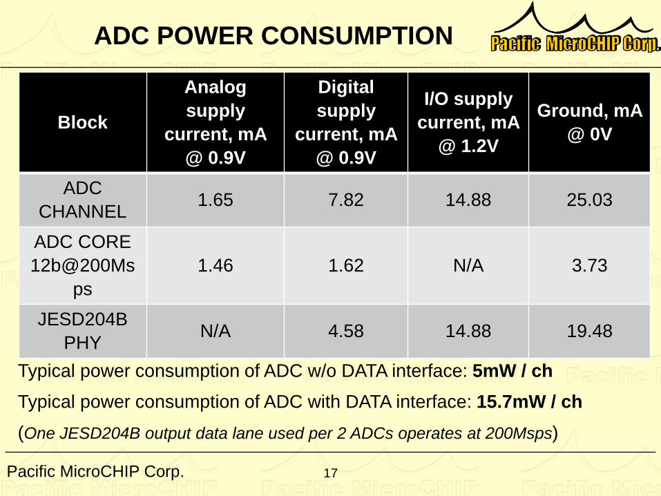
ADC POWER CONSUMPTION
Block
Analog
supply
current, mA
@ 0.9V
Digital
supply
current, mA
@ 0.9V
I/O supply
current, mA
@ 1.2V
Ground, mA
@ 0V
ADC
CHANNEL1.65 7.82 14.88 25.03
ADC CORE
12b@200Ms
ps
1.46 1.62 N/A 3.73
JESD204B
PHYN/A 4.58 14.88 19.48
Typical power consumption of ADC w/o DATA interface: 5mW / ch
Typical power consumption of ADC with DATA interface: 15.7mW / ch
(One JESD204B output data lane used per 2 ADCs operates at 200Msps)
17
Pacific MicroCHIP Corp.
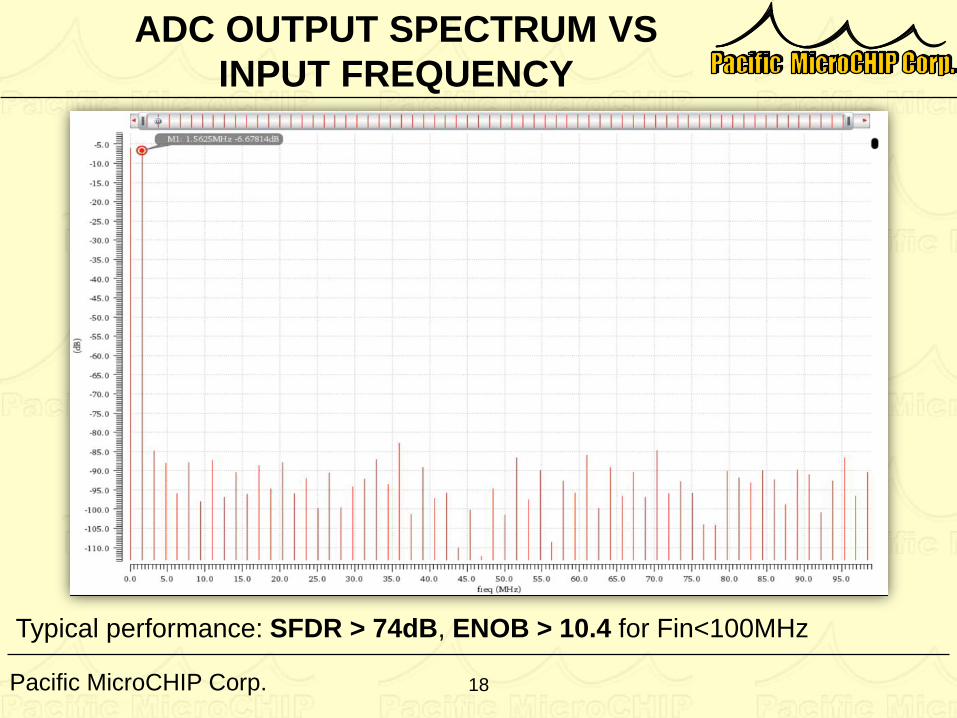
ADC OUTPUT SPECTRUM VS
INPUT FREQUENCY
Typical performance: SFDR > 74dB, ENOB > 10.4 for Fin<100MHz
18
Pacific MicroCHIP Corp.
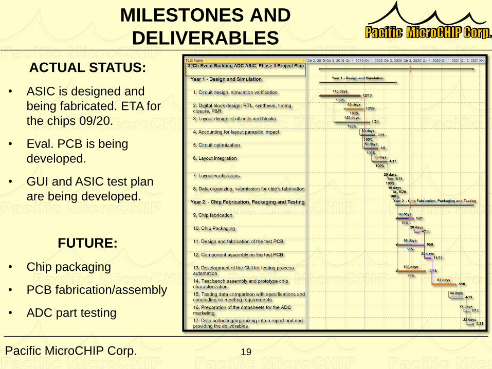
MILESTONES AND
DELIVERABLES
ACTUAL STATUS:
• ASIC is designed and
being fabricated. ETA for
the chips 09/20.
• Eval. PCB is being
developed.
• GUI and ASIC test plan
are being developed.
FUTURE:
• Chip packaging
• PCB fabrication/assembly
• ADC part testing
19
Pacific MicroCHIP Corp.
Thank You
Application Ideas for the ADC ASIC are appreciated!
20