Embed Size (px)
Citation preview
16
An Analogue Front-End System with a Low-Power On-Chip Filter and ADC for Portable ECG Detection Devices
Shuenn-Yuh Lee1, Jia-Hua Hong1, Jin-Ching Lee2 and Qiang Fang3
1Department of Electrical Engineering, National Chung-Cheng University, Taiwan 2Department of Biotechnology, College of Life Science, Kaohsiung Medical University,
3Department of Electrical and Computer Engineering, RMIT University, 1,2Taiwan
3Australia
1. Introduction
Medical diagnostic instruments can be made into portable devices for the purpose of home
care, such as the diagnosis of heart disease. These assisting devices are not only used to
monitor patients but are also beneficial as handy and convenient medical instruments.
Hence, for reasons of both portability and durability, designers should reduce the power
consumption of assistant devices as much as possible to extend their battery lifetime.
However, achieving the low power requirement of the ECG sensing and the processing
board for the ECG with commercial discrete components (A21-0003) is difficult because the
low power consumer electronics for ECG acquisition systems are not yet available. With the
help of the integrated circuit technology, the power-saving requirement of portable and
durable equipment gives circuit designers the impetus to reduce the power consumption of
analogue front-end circuits in ECG acquisition systems. In addition, the analogue front-end
circuits, which are the interface between physical signals and the digital processor, must be
operated at a low-supply voltage to be integrated into the low-voltage system-on-a-chip
(SOC) system (Eshraghian, 2006). Therefore, the chapter will present two design examples of
low-voltage (1 V) and low-power (<1 W) on-chip circuits including a low-pass filter (LPF)
and an analogue-to-digital converter (ADC) to demonstrate the possibility of developing the
low-voltage low-power ECG acquisition SOC.
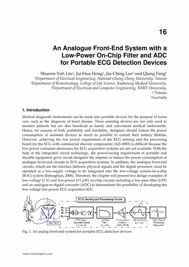
Fig. 1. An analog front-end system for portable ECG detection devices
www.intechopen.com
Advances in Electrocardiograms – Methods and Analysis
298
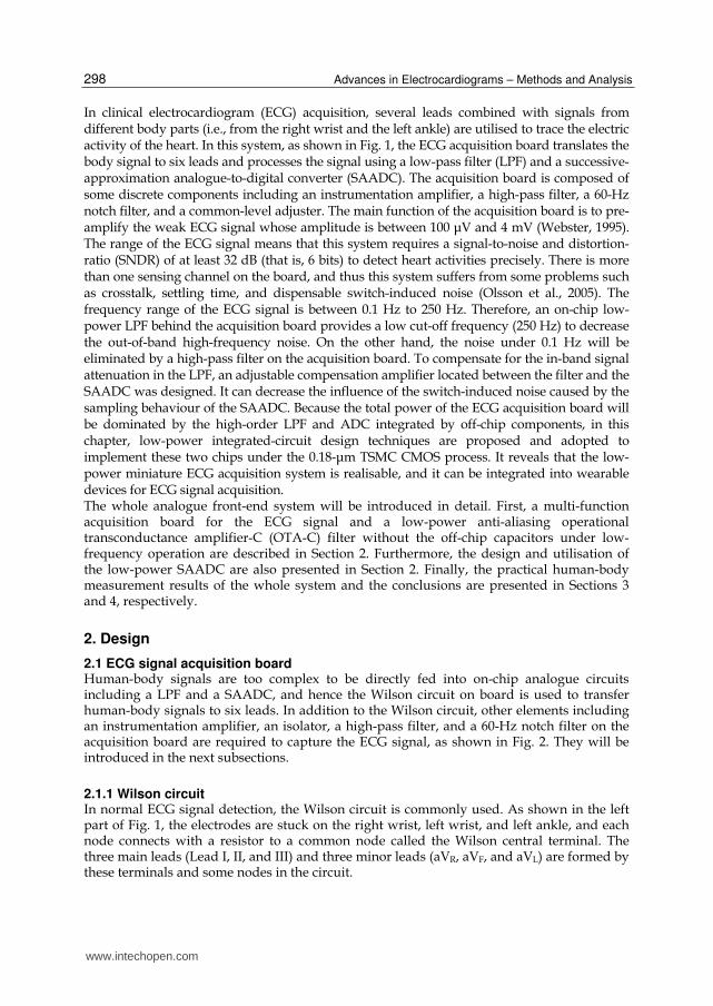
In clinical electrocardiogram (ECG) acquisition, several leads combined with signals from different body parts (i.e., from the right wrist and the left ankle) are utilised to trace the electric activity of the heart. In this system, as shown in Fig. 1, the ECG acquisition board translates the body signal to six leads and processes the signal using a low-pass filter (LPF) and a successive-approximation analogue-to-digital converter (SAADC). The acquisition board is composed of some discrete components including an instrumentation amplifier, a high-pass filter, a 60-Hz notch filter, and a common-level adjuster. The main function of the acquisition board is to pre-amplify the weak ECG signal whose amplitude is between 100 μV and 4 mV (Webster, 1995). The range of the ECG signal means that this system requires a signal-to-noise and distortion-ratio (SNDR) of at least 32 dB (that is, 6 bits) to detect heart activities precisely. There is more than one sensing channel on the board, and thus this system suffers from some problems such as crosstalk, settling time, and dispensable switch-induced noise (Olsson et al., 2005). The frequency range of the ECG signal is between 0.1 Hz to 250 Hz. Therefore, an on-chip low-power LPF behind the acquisition board provides a low cut-off frequency (250 Hz) to decrease the out-of-band high-frequency noise. On the other hand, the noise under 0.1 Hz will be eliminated by a high-pass filter on the acquisition board. To compensate for the in-band signal attenuation in the LPF, an adjustable compensation amplifier located between the filter and the SAADC was designed. It can decrease the influence of the switch-induced noise caused by the sampling behaviour of the SAADC. Because the total power of the ECG acquisition board will be dominated by the high-order LPF and ADC integrated by off-chip components, in this chapter, low-power integrated-circuit design techniques are proposed and adopted to implement these two chips under the 0.18-μm TSMC CMOS process. It reveals that the low-power miniature ECG acquisition system is realisable, and it can be integrated into wearable devices for ECG signal acquisition. The whole analogue front-end system will be introduced in detail. First, a multi-function acquisition board for the ECG signal and a low-power anti-aliasing operational transconductance amplifier-C (OTA-C) filter without the off-chip capacitors under low-frequency operation are described in Section 2. Furthermore, the design and utilisation of the low-power SAADC are also presented in Section 2. Finally, the practical human-body measurement results of the whole system and the conclusions are presented in Sections 3 and 4, respectively.
2. Design
2.1 ECG signal acquisition board Human-body signals are too complex to be directly fed into on-chip analogue circuits including a LPF and a SAADC, and hence the Wilson circuit on board is used to transfer human-body signals to six leads. In addition to the Wilson circuit, other elements including an instrumentation amplifier, an isolator, a high-pass filter, and a 60-Hz notch filter on the acquisition board are required to capture the ECG signal, as shown in Fig. 2. They will be introduced in the next subsections.
2.1.1 Wilson circuit In normal ECG signal detection, the Wilson circuit is commonly used. As shown in the left part of Fig. 1, the electrodes are stuck on the right wrist, left wrist, and left ankle, and each node connects with a resistor to a common node called the Wilson central terminal. The three main leads (Lead I, II, and III) and three minor leads (aVR, aVF, and aVL) are formed by these terminals and some nodes in the circuit.
www.intechopen.com
An Analogue Front-End System With a Low-Power On-Chip Filter and ADC for Portable ECG Detection Devices
299
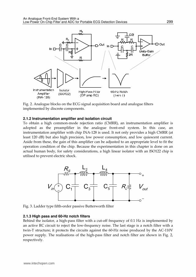
Fig. 2. Analogue blocks on the ECG signal acquisition board and analogue filters implemented by discrete components.
2.1.2 Instrumentation amplifier and isolation circuit To obtain a high common-mode rejection ratio (CMRR), an instrumentation amplifier is
adopted as the preamplifier in the analogue front-end system. In this case, an
instrumentation amplifier with chip INA-128 is used. It not only provides a high CMRR (at
least 120 dB) but also high precision, low power consumption, and low quiescent current.
Aside from these, the gain of this amplifier can be adjusted to an appropriate level to fit the
operation condition of the chip. Because the experimentation in this chapter is done on an
actual human body, for safety considerations, a high linear isolator with an ISO122 chip is
utilised to prevent electric shock.
SR
5C LR outVinV
2L
3C1C
4L
Fig. 3. Ladder type fifth-order passive Butterworth filter
2.1.3 High pass and 60-Hz notch filters Behind the isolator, a high-pass filter with a cut-off frequency of 0.1 Hz is implemented by
an active RC circuit to reject the low-frequency noise. The last stage is a notch filter with a
twin-T structure; it protects the circuits against the 60-Hz noise produced by the AC-110V
power supply. The realisations of the high-pass filter and notch filter are shown in Fig. 2,
respectively.
www.intechopen.com
Advances in Electrocardiograms – Methods and Analysis
300
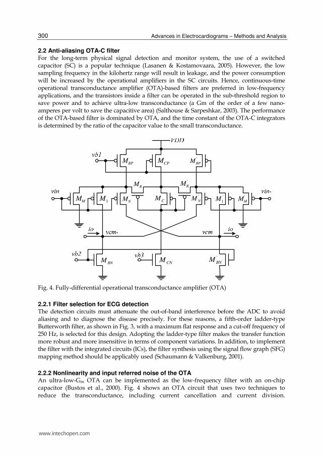
2.2 Anti-aliasing OTA-C filter For the long-term physical signal detection and monitor system, the use of a switched capacitor (SC) is a popular technique (Lasanen & Kostamovaara, 2005). However, the low sampling frequency in the kilohertz range will result in leakage, and the power consumption will be increased by the operational amplifiers in the SC circuits. Hence, continuous-time operational transconductance amplifier (OTA)-based filters are preferred in low-frequency applications, and the transistors inside a filter can be operated in the sub-threshold region to save power and to achieve ultra-low transconductance (a Gm of the order of a few nano-amperes per volt to save the capacitive area) (Salthouse & Sarpeshkar, 2003). The performance of the OTA-based filter is dominated by OTA, and the time constant of the OTA-C integrators is determined by the ratio of the capacitor value to the small transconductance.
MM
1M
'
NM
'
MM
NM
'
1M
BPM
'
BPM
BNM
'
BNM
CPM
RM
'
RM
CM
CNM
Fig. 4. Fully-differential operational transconductance amplifier (OTA)
2.2.1 Filter selection for ECG detection The detection circuits must attenuate the out-of-band interference before the ADC to avoid aliasing and to diagnose the disease precisely. For these reasons, a fifth-order ladder-type Butterworth filter, as shown in Fig. 3, with a maximum flat response and a cut-off frequency of 250 Hz, is selected for this design. Adopting the ladder-type filter makes the transfer function more robust and more insensitive in terms of component variations. In addition, to implement the filter with the integrated circuits (ICs), the filter synthesis using the signal flow graph (SFG) mapping method should be applicably used (Schaumann & Valkenburg, 2001).
2.2.2 Nonlinearity and input referred noise of the OTA An ultra-low-Gm OTA can be implemented as the low-frequency filter with an on-chip capacitor (Bustos et al., 2000). Fig. 4 shows an OTA circuit that uses two techniques to reduce the transconductance, including current cancellation and current division.
www.intechopen.com

An Analogue Front-End System With a Low-Power On-Chip Filter and ADC for Portable ECG Detection Devices
301
Furthermore, the fully differential structure provides a higher capability in terms of common-mode rejection and an increase of 3 dB in the dynamic range rather than the single-end structure. In addition, all transistors in the OTA are operated in sub-threshold region to save the power consumption. According to the analysis of the nonlinearity and input referred noise of this filter (Lee &
Cheng, 2009), the dominated third harmonic distortion (HD3) caused by the device MR can
be expressed as
3
2
2
396( )(2 )
SD
SG th F SB
vHD
v V v
(1)
where F represents the Fermi potential. In this design, HD3 is to be suppressed below -50
dB with a differential input level of 100 mV. Second harmonic distortion (HD2) is almost
cancelled by using a fully differential structure. As previously mentioned, the system
detecting the ECG signal should possess an SNDR greater than 32 dB. Because the distortion
is below 50 dB (that is, it is sufficient), the other issues in terms of equivalent input noise
should be considered in the filter design.
By selecting the PMOS as the input stage of Fig. 4, the flicker noise should be low. Given
this, the required input referred noise of the filter can be expressed as
,, ( )/20( )
10in rms
in ref SNR dB
VNoi rms (2)
According to the description, with an SNR of 42 dB (7 bits), the input referred noise must be
less than 560 Vrms for an input voltage of 100 mVrms.
inv
0mG
1mG
amG
2
bmG
2
amG
3
bmG
3
2C
1C
3C
amG
4
bmG
4
amG
5
bmG
5
4C
6mG 5
Coutv
a
'a
b
'b'cc
d
'd
e
'e
ea ~
'~' ea
Fig. 5. Active circuit realization of the fifth-order Butterworth filter
2.2.3 Fifth-order OTA-C low-pass filter The realisations of the fifth-order OTA-C filter with common-mode feedback (CMFB)
circuits are illustrated in Fig. 5. To contrast with the ladder type, the overall circuit is
composed of two grounded resistors Gm0 and Gm6, two gyrators A and B, which implement
the equivalent inductors L2 and L4, respectively, and five capacitors C1~C5. To reduce the
www.intechopen.com

Advances in Electrocardiograms – Methods and Analysis
302
power consumption, five common-mode feedback circuits are shared by the eleven OTAs of
the filter. The common-mode feedback circuits provide sensing of the common output
voltages on nodes a~e to control the bias voltage vb3 of the OTA.
2.3 Low-power successive approximation ADC For the required performance of ECG signals with an amplitude between 100 μV and 4 mV
(Webster, 1995), the resolution of the ADC with analogue filter in this ECG signal processing
system usually only has to be between 6 to 8 bits. In this chapter, a low-power SAADC with
8-bit resolution and 10-KHz sampling frequency is designed. It is not only applied to the
ECG signal, but also used for other physical signals, such as Electroneurography (ENG). The
basic architecture of a SAADC is illustrated in Fig. 6. The converter consists of a
sample/hold (S/H) circuit, a comparator, a successive approximation register (SAR)
controller, and an 8-bit digital-to-analogue converter (DAC). Using a binary searching
algorithm, the input sample voltage can be successively approximated by the DAC output
voltage. For a N-bit SAADC, N cycles are required to convert the analogue signals into
digital codes. Obviously, the DAC dominates the accuracy and the speed of the SAADC. To
conform to the system specifications, a low-power, opamp-free, capacitor-based DAC with
an 80-kHz sampling rate is implemented. The sub-circuit design of the SAADC will be
described in the following subsections in detail.
Comparator SAR
Reset
DAC
Vref
Comparator Reset
dacret
clock StartSHclock
VholdVIN
delay
D0 ~ D7
StartClock
Reset
D0 ~ D7
Vbias
Vref
Fig. 6. Block diagram of a successive approximation ADC.
Fig. 7. (a) Passive S/H circuit with dummy switch, and (b) Comparator circuit
www.intechopen.com
An Analogue Front-End System With a Low-Power On-Chip Filter and ADC for Portable ECG Detection Devices
303
2.3.1 Sample/hold circuit To decrease the power consumption of the SAADC, a passive S/H circuit illustrated in Fig. 7(a)
is adopted. It consists of the NMOS switch S1 and the sampling capacitor CH. A dummy switch
S2 is adopted to circumvent the problem of the charge injection and the clock feedthrough and
to compensate for the charge error. It will meet the requirements of 8-bit resolution.
2.3.2 Comparator circuit The comparator used in the SAADC is illustrated in Fig. 7(b); it is a track-and-latch stage. Because the accuracy of the comparator plays a critical role in the SAADC, the transistors Ms1 and Ms2 are included to avoid hysteresis or delayed response when resetting the phase. The operational principle is as follows. When the clock is high, the comparator is operated in the resetting mode, and both outputs (VOUT+ and VOUT-) are pulled to VDD (high). On the other hand, when the clock is low, the circuit will execute the comparison of differential input, and the outputs level (VOUT+ or VOUT-) of the comparator will depend on the difference between VIN+ and VIN-. The design of the bias current Ib is critical for the performance of the comparator, including speed, noise, and power consumption. For speed considerations, the frequency response of the comparator depending on the dominant pole should be analysed. The dominated pole of the comparator is located at node P and can be described as follows:
13 2 4 _ 2 , m
P P gs db db db s bufferP
gC C C C C C
C (3)
where Cp is the total capacitance at node P. To fit the 10 kS/s sampling rate of the 8-bit
SAADC, the speed of the comparator must be operated at no less than 80 kHz. However, for
settling within the 0.1% accuracy, the required unity-gain bandwidth of the comparator must
satisfy seven times its time constant. Therefore, a comparator with a unity-gain bandwidth of 1
MHz is implemented. Hence, a comparing time of less than 1 μs can be achieved.
Fig. 8. Architecture of an 8-bit capacitor-based DAC.
Because the operational speed of the comparator is at a low frequency, flicker noise will dominate the input-referred noise. Hence, a low bias current with large channel width is appropriate to decrease power consumption. In this chapter, a bias current with only 400 nA is adopted to let the comparator operate in the sub-threshold region under the 8-bit and 10-kHz requirements.
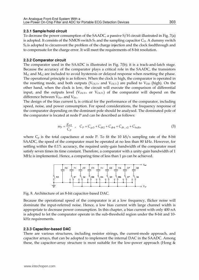
2.3.3 Capacitor-based DAC There are various structures, including resistor strings, the current-mode approach, and capacitor arrays, that can be adopted to implement the internal DAC in the SAADC. Among these, the capacitor-array structure is most suitable for the low-power approach (Hong &
www.intechopen.com

Advances in Electrocardiograms – Methods and Analysis
304
Lee, 2007). Therefore, in this chapter, an opamp-free, capacitor-based approach, as shown in Fig. 8, is used to implement the DAC. Based on the binary-weighted capacitor array, the output voltage of the DAC can be described as follows:
8
1i j j
j iout ref
total
C D C
V VC
(4)
where Ctotal is the total capacitance of the DAC, and the value of i is from 0 to 7. The power source of the above mentioned passive capacitor array is dominated by the reference voltage, Vref. It can be analysed by calculating the required charge of all the capacitors during charging and discharging periods (Hong & Lee, 2007). A relative equation described below can be used to estimate the power:
8 2 20
5 12
9 6 2clk
Vref DD in
fP C V V
(5)
where fclk is the operational frequency of the DAC, Vin is the sampling voltage of the S/H circuit, and C0 is the unity capacitor. According to (5), a smaller capacitor, C0, can reduce power consumption. However, it will also contribute to an increase in thermal noise (KT/C), which degrades the resolution of the DAC. In this chapter, a metal-insulator-metal (MIM) capacitor of 24 fF is implemented in a TSMC 0.18-μm 1P6M CMOS process to trade off between power consumption and the noise contribution.
Fig. 9. N-bit SAR controller based on the non-redundant structure.
Moreover, the matching and noise in the capacitor array will dominate the accuracy of the DAC. However, the process variation resulting in matching error commonly plays a more important role compared with the thermal noise. Hence, the layout of the capacitor array based on the common-centroid structure is adopted to protect against the matching error.
2.3.4 SAR Controller For a N-bit SAR, two sets of registers are required in the binary search algorithm. One is used for storing the conversion results, and the other is used for estimating the results. A non-redundant structure, as illustrated in Fig. 9, is adopted to reduce the usage of the registers; the result is to reduce power consumption (Rossi & Fucili, 1996). In this structure,
www.intechopen.com

An Analogue Front-End System With a Low-Power On-Chip Filter and ADC for Portable ECG Detection Devices
305
a finite state machine (FSM) is used to generate the control signal. At the beginning of conversion, the most significant bit (MSB) is set to one, whereas the remaining bits are set to zero. The initial value of the DAC output is then set to 0.5 V (1/2 full scale). If the comparator output is low, the MSB will be set to 0 and saved in the output of the SAR. If the output is high, the MSB will remain 1. The residue bits will be processed in the same operations until the least significant bit (LSB) is determined.
3. Experimental results
The three main elements introduced above were integrated to a low-power analogue front-
end system on a detection board; the measured analogue front-end system was set up as
shown in Fig. 10. The picture also shows the practical measurement conditions: the
electrodes are stuck on both wrists and both ankles. The circuits of the OTA-C filter and
SAADC were fabricated in a 0.18-μm TSMC process with metal-insulator-metal (MIM)
capacitors. The die area of the OTA-C filter and SAADC are 0.135 mm2 and 0.12 mm2,
respectively. Figure 10 also shows the microphotographs of the two chips.
320µm
284µm
Fig. 10. Chip-microphotographs of an OTA-C filter and SAADC, respectively, and the measurement setup of an analog front-end ECG detection system
3.1 Filter measurement A differential sinusoidal wave with a magnitude of 100 mVPP is fed into the chip to measure
the frequency response and the power spectrum with an input frequency of 50 Hz. Referring
to Fig. 11(a), the -3 dB frequency is around 240 Hz, where the inband gain degradation (from
-6 dB to -10 dB) arises from the finite-gain effect of the OTA. The measured third harmonic
distortion (HD3) in Fig. 11(b) is well below -49 dB, which is close to the simulation
estimation. In addition, the integrated input referred noise from 1 - 250 Hz is 340 µVrms. The
power consumption is 453 nW at a supply voltage of 1 V.
www.intechopen.com

Advances in Electrocardiograms – Methods and Analysis
306
102
103
-70
-60
-50
-40
-30
-20
-10
0
Frequency (Hz)
Ma
gn
itu
de
(d
B)
Frequency Response of the OTA-C Filter
(a) (b)
Fig. 11. Measurement of the OTA-C filter. (a) Frequency response. (b) Output power spectrum density.
3.2 SAADC measurement The 1-kHz input signal with a 500-mVpp full-swing magnitude sinusoidal wave is fed into
the SAADC to measure integral nonlinearity (INL) and differential nonlinearity (DNL).
Moreover, the sampling rate is 10 kHz. Fig. 12 shows the maximum DNL is +0.38/-0.41 LSB,
whereas the maximum INL is +0.6/-0.89 LSB. Moreover, a full-scale 100-Hz sine-wave
spectrum measured at a 1-kHz sampling rate is illustrated in Fig. 13 to demonstrate the low-
frequency performance. The signal-to-noise distortion ratio (SNDR) in the ECG bandwidth
(250 Hz) is 48.46 dB, and the spurious free dynamic range (SFDR) is 57 dB. Meanwhile, the
effective number of bits (ENOB) defined as follows is 7.76 bits:
1.76
6.02
SNDRENOB
(6)
Fig. 12. Measured DNL and INL of the SAADC
www.intechopen.com

An Analogue Front-End System With a Low-Power On-Chip Filter and ADC for Portable ECG Detection Devices
307
50 100 150 200 250 300 350 400 450 500
-120
-100
-80
-60
-40
-20
Spectrum of 8-bit SARADC
[dB
]
SNDR=48.4627 dB ;ENOB=7.75792 bit
Fig. 13. Measured output spectrum at 100Hz input frequency and 1 kHz sampling rate.
Fig. 14. Measurement results of the ECG analog front-end system
3.3 Real ECG signal testing Corresponding to the system shown in Fig. 1, the measurement results are also illustrated in Fig. 14. They are measured from each output node of the three main partitions on the system, including (a) the ECG acquisition board, (b) the OTA-C filter, and (c) the SAADC. We can observe the relations and functions between each output. Channel 1 in Fig. 14 is the initial pre-amplified ECG signal with obvious high-frequency noise generated by the human body. Because some tiny physical waves are covered, this kind of ECG signal is inconvenient for the diagnosis of heart disease. With the help of the low-pass OTA-C filter, the high frequency noise can be significantly attenuated, and the tracing signal with a clear baseline is shown in channel 2. To demonstrate the operation of the SAADC, the waveform view showing in the logic analyser is adopted to present the conversion result. Channel 3 in Fig. 14 shows the real-time human-body digital ECG waveform reconstructed by the 8-bit decimal codes of the SAADC. Similarly, a clear baseline is observed in this graph, and the 8-bit digital codes can be accepted by the post digital processor to diagnose the abnormal heart activities precisely.
www.intechopen.com

Advances in Electrocardiograms – Methods and Analysis
308
4. Conclusions
A low-power analogue front-end system for ECG detection consisting of an acquisition board and two low-power on-chip components is presented. The design issues including an off-chip ECG signal acquisition board, an on-chip analogue filter, and an on-chip ADC are introduced in this chapter. The result reveals that developing an ultra low-power ECG acquisition SOC is possible. In the future, the entire elements of these three partitions will be integrated into a single chip to save area and achieve a fully low-voltage and low-power ECG acquisition SOC for wearable applications.
5. Acknowledgment
The authors would like to thank the Chip Implementation Center (CIC), the National Science Council (NSC) of Taiwan, R. O. C. under Grant NSC 99-2628-E-194-032, NSC 99-2220-E-194-001, and NSC 99-2220-E-194-006, the Australian Research Council, Australia for their support of this work, and the help of CBIC Laboratory members, Yu-Cheng Su, Chih-Jen Cheng, Kun-Min Huang, and Wei-Chun Kao.
6. References
A21-0003. ECG acquisition board. http://www.icci.com.tw Bustos S. S., Martinez J. S., Maloberti F., Sinencio E. S., (2000). A 60-dB dynamic-range
CMOS sixth-Order 2.4Hz low-pass filter for medical application. IEEE Trans. Circuits Syst. II: Analog and Digital Signal Processing, Vol. 47. No.12, (2000), pp. 1391–1398, ISSN 1057-7130.
Eshraghian K. (2006). SoC emerging technologies. Proc. IEEE, Vol. 94, No. 6, (2006), pp. 1197-1213, ISSN 0018-9219.
Hong H. C., Lee G. M. (2007). A 65-fJ/conversion-step 0.9-V 200-kS/s rail-to-rail 8-bit successive approximation ADC. IEEE J. Solid-State Circuits, Vol. 42, No. 10, (2007), pp. 2161-2168, ISSN 0018-9200.
Lasanen K., Kostamovaara J. (2005). A 1-V analog CMOS front-end for detecting QRS complexes in a cardiac signal. IEEE Trans. Circuits Syst. I: Regular Papers, Vol. 52, No. 12, (2005), pp. 2584-2594, ISSN 1057-7122.
Lee S. Y., Cheng C. J. (2009). Systematic design and modeling of a OTA-C filter for portable ECG detection. IEEE Trans. Biomed. Circuits Syst., Vol. 3, No. 1, (2009), pp. 53-64, ISSN 1932-4545.
Olsson R. H., Buhl D. L., Sirota A. M. Guzsaki G., Wise K. D. (2005). Band-tunable and multiplexed integrated circuits for simultaneous recording and stimulation with microelectrode arrays. IEEE Trans. Biomed. Eng., Vol. 52, No. 7, (2005), pp. 1303-1311, ISSN 0018-9294.
Rossi A., Fucili G. (1996). Nonredundant successive approximation register for A/D converters. Electronics Letters, Vol. 32. No. 12, (1996), pp. 1055-1056, ISSN 0013-5194.
Salthouse C.D., Sarpeshkar R. (2003). A practical micropower programmable bandpass filter for use in bionic ears. IEEE J. Solid-State Circuits, Vol. 38, No. 1, (2003), pp. 63-70, ISSN 0018-9200.
Schaumann R., Valkenburg M. E. V. ( 2001). Design of Analog Filters. New York: Oxford. Webster J. G. (1995). Design of Cardiac Pacemakers. Piscataway, NJ: IEEE Press.
www.intechopen.com

Advances in Electrocardiograms - Methods and AnalysisEdited by PhD. Richard Millis
ISBN 978-953-307-923-3Hard cover, 390 pagesPublisher InTechPublished online 25, January, 2012Published in print edition January, 2012
InTech EuropeUniversity Campus STeP Ri Slavka Krautzeka 83/A 51000 Rijeka, Croatia Phone: +385 (51) 770 447 Fax: +385 (51) 686 166www.intechopen.com
InTech ChinaUnit 405, Office Block, Hotel Equatorial Shanghai No.65, Yan An Road (West), Shanghai, 200040, China
Phone: +86-21-62489820 Fax: +86-21-62489821
Electrocardiograms are one of the most widely used methods for evaluating the structure-functionrelationships of the heart in health and disease. This book is the first of two volumes which reviews recentadvancements in electrocardiography. This volume lays the groundwork for understanding the technicalaspects of these advancements. The five sections of this volume, Cardiac Anatomy, ECG Technique, ECGFeatures, Heart Rate Variability and ECG Data Management, provide comprehensive reviews ofadvancements in the technical and analytical methods for interpreting and evaluating electrocardiograms. Thisvolume is complemented with anatomical diagrams, electrocardiogram recordings, flow diagrams andalgorithms which demonstrate the most modern principles of electrocardiography. The chapters which formthis volume describe how the technical impediments inherent to instrument-patient interfacing, recording andinterpreting variations in electrocardiogram time intervals and morphologies, as well as electrocardiogram datasharing have been effectively overcome. The advent of novel detection, filtering and testing devices aredescribed. Foremost, among these devices are innovative algorithms for automating the evaluation ofelectrocardiograms.
How to referenceIn order to correctly reference this scholarly work, feel free to copy and paste the following:
Shuenn-Yuh Lee, Jia-Hua Hong, Jin-Ching Lee and Qiang Fang (2012). An Analogue Front-End System with aLow-Power On-Chip Filter and ADC for Portable ECG Detection Devices, Advances in Electrocardiograms -Methods and Analysis, PhD. Richard Millis (Ed.), ISBN: 978-953-307-923-3, InTech, Available from:http://www.intechopen.com/books/advances-in-electrocardiograms-methods-and-analysis/an-analogue-front-end-system-with-a-low-power-on-chip-filter-and-adc-for-portable-ecg-detection-devi

© 2012 The Author(s). Licensee IntechOpen. This is an open access articledistributed under the terms of the Creative Commons Attribution 3.0License, which permits unrestricted use, distribution, and reproduction inany medium, provided the original work is properly cited.