Embed Size (px)
Citation preview
1
An Accurate, Continuous, and Lossless Self-Learning CMOS Current-Sensing Scheme for Inductor-Based DC–DC Converters
H. Pooya Forghani-zadeh, Student Member, IEEE, and Gabriel A. Rincón-Mora, Senior Member, IEEE
Georgia Tech Analog and Power IC Lab Georgia Institute of Technology
Atlanta, GA 30332, USA [email protected] and [email protected]
Abstract:
Sensing current is a fundamental function in power supply circuits, especially as it generally
applies to protection and feedback control. Emerging state-of-the-art switching supplies, in fact, are now
exploring ways to use this sensed-current information to improve transient response, power efficiency,
and compensation performance by appropriately self-adjusting, on the fly, frequency, inductor ripple
current, switching configuration (e.g., synchronous to/from asynchronous), and other operating
parameters. The discontinuous, non-integrated, and inaccurate nature of existing lossless current-sensing
schemes, however, impedes their widespread adoption, and lossy solutions are not acceptable. Lossless,
filter-based techniques are continuous, but inaccurate when integrated on-chip because of the inherent
mismatches between the filter and the power inductor. The proposed GM-C filter-based, fully integrated
current-sensing CMOS scheme circumvents this accuracy limitation by introducing a self-learning
sequence to start-up and power-on-reset. During these seldom-occurring events, the gain and bandwidth
of the internal filter are matched to the response of the power inductor and its equivalent series resistance
(ESR), effectively measuring their values. A 0.5 µm CMOS realization of the proposed scheme was
fabricated and applied to a current-mode buck switching supply, achieving overall DC and ac current-
gain errors of 8% and 9%, respectively, at 0.8 A DC load and 0.2 A ripple currents for 3.5 µH - 14 µH
inductors with ESRs ranging from 48 mΩ to 384 mΩ (other lossless, state-of-the-art solutions achieve 20-
40% error, and only when the nominal specifications of the power MOSFET and/or inductor are known).
Since the self-learning sequence is non-recurring, the power losses associated with the foregoing solution
are minimal, translating to a 2.6% power efficiency savings when compared to the more traditional but
accurate series-sense resistor (e.g., 50 mΩ) technique .
Index Terns—power management, switching regulators, DC-DC converters, current sensing, lossless,
GM-C filter, current-mode, self-learning, inductance measurement.

2
I. Introduction
Switching DC-DC converters are an indispensable component of every battery-operated
device, efficiently supplying power to all vital and supplementary blocks of the system. While it
is possible to design these switching supplies without sensing current, with only output voltage
information [1-2], short-circuit protection and increasingly stringent performance requirements
force designers to include a current-sensing function to almost all practical solutions. Boost and
buck-boost DC-DC converters, for instance, are optimally stable under the guise of a current-
mode topology, in which case sensing current eases feedback control requirements [3].
Additionally, modern state-of-the-art designs use sensed-current information to optimally set the
operating mode of the system for highest power efficiency [4]; balance the various phase loads
of multiphase converters [5]; control and regulate single-inductor, multiple-output topologies [6];
and even multiply the inductance of micro-scale power inductors [7]. The over-riding
requirements for all these applications are losslessness for increased battery life, integration for
small footprint solutions, accuracy for high performance, and in many cases, continuous
operation for maximum flexibility and optimum performance.
Achieving both losslessness and accuracy is difficult. Adding a series sense-resistor, for
instance, and sensing the voltage across it can be accurate, but necessarily lossy because it
carries all of the sensed current, which can be on the order of Amperes, reducing the overall
power efficiency of a switching supply by 2-10%. The only way to completely eliminate the
losses is by not introducing any additional series devices in the power-carrying paths of the
system, in other words, by using the components that already exist in the power stage, like the
power inductor, output capacitor, and the surrounding power switches [8]. Unfortunately,
however, the impedances of these devices vary significantly with process, temperature, vendor,
and design, and this variation translates to poor current-sensing tolerance. Nevertheless, given
the sensitive nature of battery life in portable electronics to power losses, accuracy is often
sacrificed for lifetime.
Series MOSFET’s Ron [9] and parallel current-sensing FET (sense-FET) [9-15] schemes
are among the most popular lossless sensing techniques today. In the MOSFET’s Ron case, the
voltage across a power switch is measured and divided by its estimated turn-on resistance to
extrapolate the value of the current flowing through it, when it is conducting. This resistance,
unfortunately, typically varies with temperature, process, and supply voltages by 50-200% [9]. In
3
the sense-FET scheme, a mirror transistor is used to source a fraction of the switch current, and
its accuracy is determined by the matching performance of the current mirror in triode
(Ohmic/non-saturated region), whose mirroring ratio is on the order of 1,000 or higher. Although
accuracies of ±4% are reported [15], channel-length modulation and process-induced mismatch
errors between sense- and power-FETs, whose device ratio is considerably large with minimum
channel lengths, can cause 3σ errors as large as ±20% [16]. Ultimately, sensing the switch
current is discontinuous because of the very nature of the switch, conducting current only a
fraction of the period. The noisy sensed current must therefore be synchronized and/or averaged
via a sample-and-hold network. Sensing the inductor current continuously may be achieved with
complementary sense-FETs, but the complexity and noise necessarily increase. The sense-FET,
which enjoys better matching performance, is further limited to fully integrated solutions, where
the switches are on-chip, because well-matched sense-FETs are not otherwise available.
The only means of sensing the current continuously is by altogether avoiding the
switches, which is the basic feature of the filter approach. These schemes indirectly measure the
inductor current, which is inherently continuous, by applying the inductor voltage across a tuned
low pass filter and sensing the filter current. Since there is no switching noise, the filter is better
suited for current-mode feedback control applications [9, 17]. The accuracy, however, much like
the switch-based schemes, is dependent on the tolerance of the inductance and equivalent series
resistance (ESR) of the power inductor and the tuning accuracy of the filter, whose overall
tolerance can be ±28% (inductance, ESR, and temperature variation of ±15%, ±11%, and 70 °C,
respectively) and worse for extended temperature-range applications [17].
For any lossless technique to be accurate, the circuit must sense the voltage across an
existing power device whose impedance is well-known, exploiting Ohm’s law. Unfortunately,
accuracy degrades as the sensing circuit is fully integrated on-chip, as power device tolerance
and characteristics, be it from a power switch, inductor, or capacitor, become even more
unknown (i.e., dependent on vendor and application in addition to temperature and process
technology). A self-learning scheme is therefore proposed, wherein the power inductor is
measured and characterized during start-up and/or power-on-reset events, as will be described in
Section II. The design of a 0.5 µm CMOS prototype is presented in Section III and its application
to a current-mode buck converter discussed in Section IV. Experimental results are subsequently
presented in Section V and conclusions drawn in Section VI.

4
II. Proposed Self-Learning Scheme
As just alluded, the driving force behind the proposed current-sensing scheme is to
automatically and indirectly measure the inductance and equivalent series resistance (ESR) of an
off-chip power inductor during start-up. Tuning the sensing circuit during start-up and measuring
inductor current during normal operating conditions assure both accuracy and continuous
operation. These general concepts are applied to the filter technique because of its losslessness
(i.e., no additional series sense power device is necessary), low switching noise, and high
bandwidth, assuming the tuning values are stored and the tuning circuitry disengaged during
normal operating conditions.
In the proposed solution, which is illustrated in Fig. 1, the inductor current is measured
by applying the voltage across L and RESR to a GM-C filter whose voltage frequency response
matches the current response of the inductor. The output voltage of the filter is therefore
proportional to inductor current IL [17-18]:
( ) (s)IsRC1
sL/R1RRg(s)V LESR
ESR1mSense ⎟⎠
⎞⎜⎝
⎛+
+= , (1)
where gm1 is the transconductance of the GM cell, R the filter resistor, and C the filter capacitor. If
the product of R and C is tuned to the ratio of L and RESR,
RCRL
ESR= , (2)
VSense is independent of frequency and linearly and directly proportional to IL,
( ) LESR1msense IRRgV = , (3)
where product (gm1R)RESR is the current-sensing gain, which can be calibrated to any value (e.g.,
0.5 V/A) by properly adjusting gm1 and/or R. During normal operation, RESR can change with
frequency because of skin effect but its effects are most prevalent at frequencies higher than the
switching frequency and minimal at frequencies of interest.
During each start-up and power-on-reset event, after biasing currents and voltages are
properly set, but before the switching supply is allowed to start, the tuning and calibration
circuits are engaged, properly adjusting and setting current-sensing filter parameters gm1 and R.
During this process, power switches MH and ML are both off and test current ITest is forced into
inductor L at switching node Vph. Once gm1 and R are set, they are stored and the DC-DC
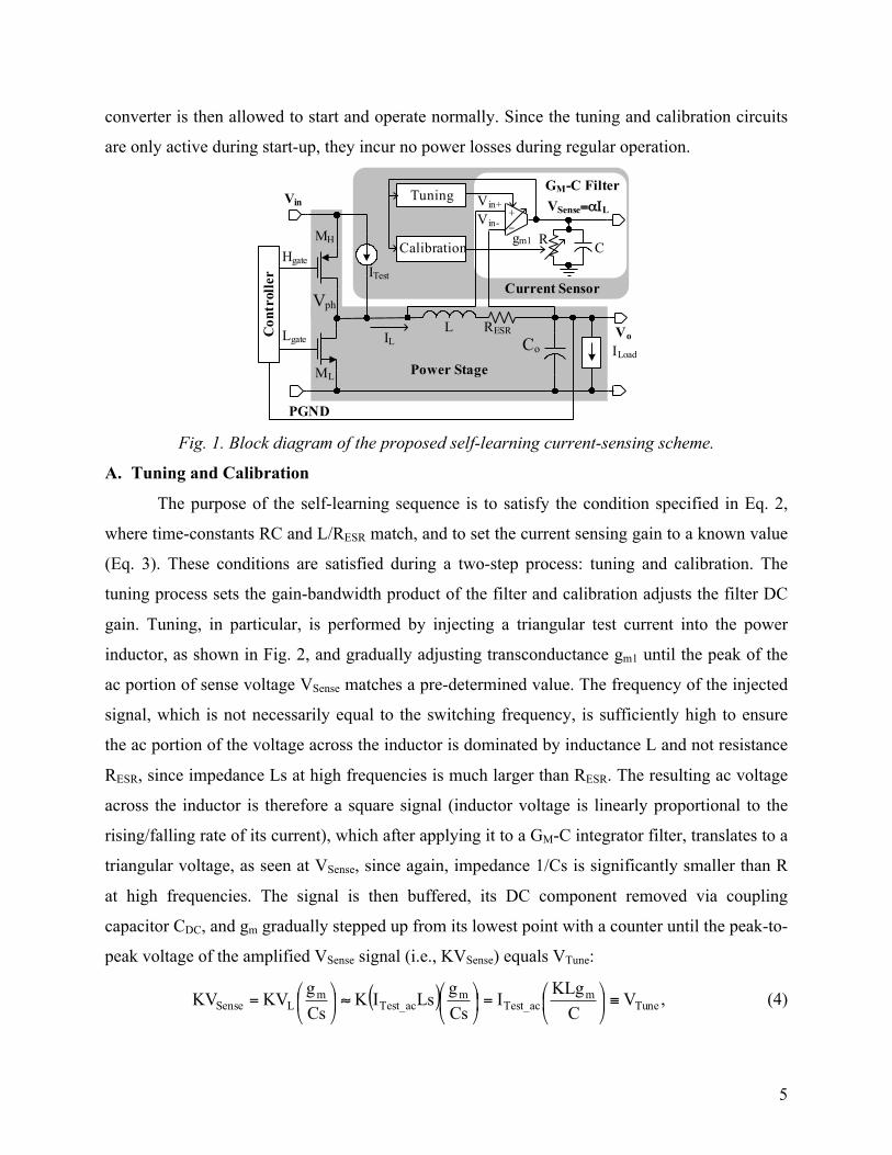
5
converter is then allowed to start and operate normally. Since the tuning and calibration circuits
are only active during start-up, they incur no power losses during regular operation.
ILoad
Vo
MH
ML
LCo
PGND
Vin
Vph
Hgate
Lgate ILRESR
Vin+
gm1
+-
R C
VSense=αΙL
GM-C Filter
Vin-
ITest
Tuning
Calibration
Current Sensor
Power Stage
Con
trol
ler
Fig. 1. Block diagram of the proposed self-learning current-sensing scheme.
A. Tuning and Calibration
The purpose of the self-learning sequence is to satisfy the condition specified in Eq. 2,
where time-constants RC and L/RESR match, and to set the current sensing gain to a known value
(Eq. 3). These conditions are satisfied during a two-step process: tuning and calibration. The
tuning process sets the gain-bandwidth product of the filter and calibration adjusts the filter DC
gain. Tuning, in particular, is performed by injecting a triangular test current into the power
inductor, as shown in Fig. 2, and gradually adjusting transconductance gm1 until the peak of the
ac portion of sense voltage VSense matches a pre-determined value. The frequency of the injected
signal, which is not necessarily equal to the switching frequency, is sufficiently high to ensure
the ac portion of the voltage across the inductor is dominated by inductance L and not resistance
RESR, since impedance Ls at high frequencies is much larger than RESR. The resulting ac voltage
across the inductor is therefore a square signal (inductor voltage is linearly proportional to the
rising/falling rate of its current), which after applying it to a GM-C integrator filter, translates to a
triangular voltage, as seen at VSense, since again, impedance 1/Cs is significantly smaller than R
at high frequencies. The signal is then buffered, its DC component removed via coupling
capacitor CDC, and gm gradually stepped up from its lowest point with a counter until the peak-to-
peak voltage of the amplified VSense signal (i.e., KVSense) equals VTune:
( ) Tunem
Test_acm
Test_acm
LSense VCLgKI
CsgLsIK
CsgVKVK ≡⎟
⎠
⎞⎜⎝
⎛=⎟⎠
⎞⎜⎝
⎛≈⎟⎠
⎞⎜⎝
⎛= , (4)

6
at which point comparator CMP stops the clock and stores the value. The buffer introduces gain
K to increase the tuning resolution of CMP because the peak-to-peak current ripple of ITest is low
and subsequently so is the ac amplitude of VSense.
Clk
VComp
RESR
+-
gm
RC
VSense
ITest_ac
-
+KCDC
Vtune
VPreamp
Q()
Counter
L
Preamp
CMP
VLGM-C Filter DC
Removal
Stop
Fig. 2. Block diagram of the tuning phase.
As a side note, R is kept at its minimum value during this part of the process to reduce
DC offsets in the system and consequently relax the DC-blocking performance requirements of
CDC (i.e., reduce the order of the high pass filter). Ideally, the test frequency should be close to
the switching frequency of the regulator to ensure L is measured close to the operating frequency
because inductance may be different at two frequencies. However, experiments only showed a
1% per decade decrease in inductance, which for a tuning frequency of 100 kHz and a converter
operating frequency of 1 MHz amounts to 1% error.
In the calibration phase, which immediately follows the tuning cycle, a DC current is fed
into the inductor, DC-blocking capacitor CDC is removed, and R is gradually increased from its
minimum point with a counter until the output of the pre-amplifier reaches VCal, as shown in Fig.
3. Since the voltage across RESR overwhelms that of L because impedance Ls is much lower than
RESR and only DC values exist, the amplified version of VSense (i.e., KVSense) is adjusted until it
equals calibration voltage VCal,
( ) ( )( ) CalmDCTest_ESRmLSense VKRgIRKRgVVK ≡≈= . (5)
If tuning and calibration reference impedances VTune/ITest_ac and VCal/ITest_DC match,
RKgRIV
CLgK
IV
mESRTest_DC
Calm
Test_ac
Tune ≈≡≈ , (6)
GM-C filter time-constant RC equals inductor time-constant L/RESR, which corresponds to the
targeted condition prescribed by Eq. 2, and current sensing is possible:

7
( ) LLTest_DC
CalLESRmsense II
IKVIRRgV α≡⎟
⎟⎠
⎞⎜⎜⎝
⎛≈= , (7)
where Eqs. 3 and 6 are recombined and α is the overall current-sensing gain of the circuit.
VComp
ITest_DC
+-
gm
RC
VSense
-
+K
Vcal
VPreamp
Clk
Counter
L
Q()
Preamp
CMP
VL GM-C Filter
Stop
RESR
Fig. 3. Block diagram of the calibration phase.
B. Error Sources
The accuracy of the foregoing technique is dependent on tuning and calibration accuracy.
Consequently, the ac and DC sensing errors are the result of the tuning and calibration loops,
respectively, which are in turn affected by the input-referred offsets of the GM cell, comparator
CMP, and the pre-amplifier; the tolerance of VCal, VTune, ITest_DC, and ITest_ac and the resolution or
quantization error of sensing parameters gm and R (minimum five bits of resolution were used,
which translates to maximum of 3.2% quantization error). Because test currents cannot exceed
reasonable levels and the resulting test voltage across the power inductor is low (on the order of
1-5 mV), overall sensing accuracy is particularly sensitive to the input-referred offset of the GM
cell. Currents over 50 mA, for example, which would increase the magnitude of the signal,
require significant die area overhead and result in parasitic hot spots that not only affect the self-
learning results but also unnecessarily push the thermal limits of the package. The end result is
that the GM cell must incorporate a dynamic offset-canceling feature [19].
Another source of error is drift, when inductance and/or ESR change from their self-
learned values. This variation may be the result of temperature, power level, and/or wear and
tear. Of these, the temperature coefficient (TC) of the ESR, which is approximately 3,900
ppm/oC (TC of copper), has the worse effect [17], on the order of ±20% for every 100 oC.
Fortunately, this error is systematic and linear, and can therefore be compensated by including it
in the system. A simple way to compensate for temperature errors is to use a proportional to

8
absolute temperature (PTAT) VCal voltage source in the calibration loop with its temperature
coefficient equal to the of the ESR. Similarly, when processing the DC output voltage of the
current-sensing filter, VSense should also be compared against a PTAT voltage source, not a
temperature-independent voltage. The errors caused by variations in other operating point
conditions, such as inductance changes with temperature, are negligibly small [17] and can be
compensated during each startup and/or power-on-reset event.
III. Current-Sensing Circuit
A. GM-C Filter
The GM-C filter is a first-order, low pass filter (Fig. 1) with a programmable gain and
bandwidth feature (variable gm and filter resistor R) [20]. As discussed earlier, because of low
ESR values, the voltage across the inductor is small and on the order of tens of milli-Volts (i.e., 1
A load current transient into an ESR of 50 mΩ produces a 50 mV drop). The situation is even
worse during startup, when relatively small test currents (i.e., 50 mA) are used, resulting in test
signals at the input of the filter on the order of 1-5 mV, thereby requiring low offset
performance. Since the goal is continuous operation, which is useful in current-mode controllers
and other high performance applications, the offset-cancellation technique must also be
continuous.
The proposed continuous low offset GM-C filter is illustrated in Fig. 4 and is comprised
of two well-matched, auto-zeroed, ping-ponging [19] dual-input summing transconductors (i.e.,
GM1 and GM2); two offset-programming capacitors for each transconductor (i.e., Ch1-, Ch1+, Ch2-,
and Ch2+); a single bandwidth-setting capacitor C; gain-setting resistor R; and non-overlapping
clock signals φ and φn. The non-overlapping feature is implemented to prevent various cross-
wiring events. Input voltage Vref, against which filter output voltage Vo is referenced, is used as a
virtual ground (ac ground). Finally, as in all ping-pong schemes, while one transconductor
processes the input signal, the other one auto-zeroes.
The difference in the proposed offset-cancellation scheme with state-of-the-art is that a
summing amplifier is used to program and cancel the offset by dedicating an input differential
pair to the input signal and another to subtract (i.e., cancel) the offset. The key advantage to this
configuration is that the large holding capacitor is de-coupled from the high bandwidth path, that
is to say, not connected to the input ac-signal path and therefore not bandwidth-limiting the

9
signal. A large holding capacitor is desirable because it reduces clock feed-through and charge
injection, consequently improving offset cancellation performance, all without adversely
affecting bandwidth.
R
Vo
Vref
Ch1-
Ch2-
C
GM1
GM2
+
-+
ϕ
Ch1+
+
-+
Vo1
Vo2
Vaux1-
Vaux2-
Vref
Vid
ϕ
ϕϕnϕϕn
ϕn
ϕ
ϕn
ϕ
ϕ
ϕn
ϕn
-Ch2+
Vref ϕn
-a
a
Fig. 4. Auto-zeroed, ping-ponging GM-C filter circuit.
In the switching supply circuit shown in Fig. 1, the GM-C filter must be programmable
and highly linear across the rail-to-rail input voltage range. Since the non-inverting input
periodically swings from the positive to the negative supply, a variation in transconductance
(Δgm) in these two states translates to a systematic input-referred offset error voltage (Vos_gm),
idm
m
m
mid
m
oos_gm V
gΔg
RgRΔgV
RgΔVV ⎟⎟
⎠
⎞⎜⎜⎝
⎛=== , (8)
where Vid is the differential voltage applied to the transconductor [8, 20]. Parasitic voltage
artifacts present in the non-inverting input signal like inductive ringing are filtered by the low
frequency GM-C filter (just as L filters these same non-idealities from affecting the inductor
current) and therefore have little to no effects on offset or circuit operation. Similarly, since dead
time introduces short-lived parasitic diode voltage drops to this signal, its effects are also filtered
and therefore relatively inconsequential. In fact, since this signal is applied to both inductor
(current filter) and GM-C circuit (voltage filter), its parasitic effects on inductor current are
reproduced by the current-sensing block, further validating the sensing capability of the circuit.
Because polysilicon resistors are many times more linear than transistors and the non-
inverting input of the transconductor is connected to a low impedance node (i.e., connected to a
source capable of supplying current), a wide input voltage range resistor-dependent current
conveyor [21-23], as shown in Fig. 5, can be used in place of a traditional differential pair

10
transconductor. The input terminals of amplifier Aint are virtually short-circuited because of
negative feedback and the resulting current flowing through series resistor R1 (IR1) is
proportional to the differential input voltage applied to the GM-C cell (Vid),
1
idR1 R
VI = . (9)
The current conveyor converts the large voltage variations across the inductor into current,
thereby not affecting the voltage biasing point of differential amplifier Aint, whose input
terminals remain biased at the regulated output voltage of the converter (Aint’s non-inverting
input). The wide voltage swing is only applied across a polysilicon resistor, which has a
relatively low voltage coefficient (e.g., 50 ppm/V) and therefore negligible adverse effects on the
circuit. This current is then mirrored to the output by current mirror M1-M2, ultimately defining
the transconductance to
11
id
idid
om R
KRKV
V1
VIg =⎟⎟
⎠
⎞⎜⎜⎝
⎛=≡ , (10)
where K is a digitally programmable current-mirror gain.
The gate of M4 is high impedance and is therefore the gain- and bandwidth-setting node
of the current-mirror’s controlling feedback loop. Compensation capacitor Cc ensures the
bandwidth-setting pole is at sufficiently low frequencies to prevent parasitic high frequency
poles from compromising stability. This M4-M1-M3 feedback loop, however, adds a parasitic
high frequency pole to the signal-flowing path (Vid to Io) approximately at its gain-bandwidth
product (gm1/Cc), and Cc is therefore selected to balance stability against high bandwidth.
Because of the current-conveyor configuration (i.e., amplifier Aint’s inverting input is
approximately equal to Aint’s non-inverting input), Aint’s input common-mode range need only
include the regulated output voltage range of the converter (non-inverting input voltage range),
which superimposes relatively relaxed input common-mode range requirements on Aint. Aint, as
shown in Fig. 5(b), is therefore a standard ground-sensing two-stage PMOS input differential
amplifier with a Miller-compensating (CINT) capacitor that produces a gain-bandwidth product of
10 MHz, which constitutes another parasitic pole in the signal-flowing path from Vid to Io.

11
-
+-
+vo
Ib KIb
I1
M1 M2
M3 M4
CurrentSource
(W/L)
d6-d0
d6-d0
gma
K(W/L)
CurrentMirror
R1
Ib2
I2
I3 I4
vG
Aint
CcVid
Vida
+
-
idamaid1
o VgVRKI +=
(a)
vssa
vdda
- +
O
P1P2
N2 N1 N3
P3 P4 P5P6
Ib
CINT
(b)
Fig. 5. (a) Linear dual-input transconductor cell and (b) Aint implementation.
The programmable K-gain current mirror implemented with M1-M2 and its slave current
source KIb are shown in Fig. 6, where a digital word determines the connectivity of the binarily
weighted array of current mirrors. Cascoding devices are added to the current mirrors and
sources to increase their respective output impedances and consequently increase the
transconductor’s overall output impedance. For functional and therefore power and real-estate
efficiency, the bias current generator and the auxiliary transconductor are combined into a single
circuit via transistor current-mirror pairs Pa-P1 and Pb-P2, where amplifier A2 equates the drain
voltages of P1 and P2 to minimize channel-length modulation errors and at the same time
properly set the biasing voltage of the gates of the upper cascoding devices. The auxiliary pair
consists of current-canceling differential pairs Na-Nb and Nc-Nd, whose net result is a low
transconductance value (gma_d) [19] that is then multiplied by current gain K with Pb-P2x mirror:
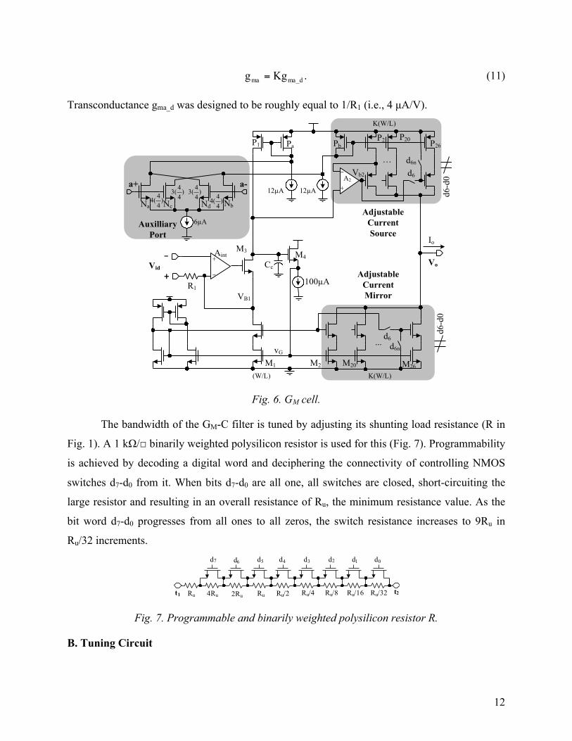
12
ma_dma Kgg = . (11)
Transconductance gma_d was designed to be roughly equal to 1/R1 (i.e., 4 µA/V).
-
+
Vo
M1 M2
M3 M4
(W/L)
d6-d
0
K(W/L)
AdjustableCurrentMirror
R1
vG
Aint
Cc
Io
M20
...
M26
VB1
PaP1
12µA
PbP2 P26
P20
…Vb2
a+ a-
d6d6n
d6-d
0
K(W/L)
-
+
-
+A2
d6
d6n
6µA
Na Nc Nd Nb)
444( )
444(
)443()
443(
Auxilliary Port
AdjustableCurrentSource
Vid
12µA
100µA
Fig. 6. GM cell.
The bandwidth of the GM-C filter is tuned by adjusting its shunting load resistance (R in
Fig. 1). A 1 kΩ/□ binarily weighted polysilicon resistor is used for this (Fig. 7). Programmability
is achieved by decoding a digital word and deciphering the connectivity of controlling NMOS
switches d7-d0 from it. When bits d7-d0 are all one, all switches are closed, short-circuiting the
large resistor and resulting in an overall resistance of Ru, the minimum resistance value. As the
bit word d7-d0 progresses from all ones to all zeros, the switch resistance increases to 9Ru in
Ru/32 increments.
Ru 4Ru 2Ru Ru Ru/2 Ru/4 Ru/8 Ru/16 Ru/32t1 t2
d1d2d3d4d5d6 d0d7
Fig. 7. Programmable and binarily weighted polysilicon resistor R.
B. Tuning Circuit

13
For ease, only one of the two ping-ponging GM cells is used during the tuning and
calibration process, as illustrated in Fig. 8(a). The subsequent pre-amplifier is a two-stage,
Miller-compensated op-amp in a non-inverting feedback configuration with a closed-loop gain of
26 dB (less than 0.1 dB of gain error) and a bandwidth of 1 MHz (five times higher than the
frequency of the triangular test signal). It drives the high pass, DC-blocking filter, which has a 3
dB bandwidth of 20 kHz (Rf is 1 MΩ and Ch21 is 8 pF). The output of the filter is then fed to an
auto-zeroed comparator with a propagation delay of 40 ns for an overdrive input signal of 10
mV. The comparator is also a standard two-stage Miller-compensated amplifier to ensure it is
stable during its auto-zeroing phase.
Vref-Vtune
VSense
Vref
φ1n
φ1
RC
φ1n
SW1
SW2
-
+
-
+
Vref190K10K
Vref
Ch21
Ch22
Vref
φ1
Q()clk
RSTEN Tuning Counter
Tune_RSTTune_EN
SW1
Tune_stop
φ1
Cmp+
Cmp-
clk
RST
ovRf
φ1
3-bit Counter
AZ_CMPPre-Amp
φ1φ1n
CMPo
Tune_stop
SW1, φ1
Tune_EN
Tune_RST
CMP+
CMP-
CMPo
Vref
Ch
Ch φ1φ1
Vin+ SW1
SW2
Vin-
Gm-C FilterTuning Circuit
SW2, φ1n
Time(s)
(a)
(b)
Vref
gm12
+
-+
-
Fig. 8. (a) Tuning circuit and (b) its relevant waveforms.
Functionally, once the tuning process is engaged by Tune_RST and Tune_EN, the tuning
counter is reset and allowed to count, gradually increasing gm1 and therefore increasing the
triangular ripple voltage seen at the input of auto-zeroed comparator AZ_CMP (Fig. 8(b)). This

14
process continues until the peak ripple voltage reaches tuning voltage VTune, at which point the
tuning counter stops (Tune_stop transitions to a high state) and gm1 is set. In the tuning sequence,
auto-zeroing clock signals φ1 and SW1 are in phase, and so are φ1n and SW2, but not so in
calibration, which is why they are separated here. When SW1 is high, both the GM cell and
AZ_CMP are auto-zeroed (i.e., connected in a unity-gain configuration to measure their
respective offset voltages and store them in holding capacitors); the triangular test signal is then
processed when SW1 is low.
A 3-bit counter is placed at the output of the buffered comparator for deglitching
purposes, to avoid noise glitches from inadvertently stopping the tuning sequence. The output of
the comparator is continually low when the peak-to-peak voltage of the triangular signal is not
sufficiently amplified. When gm1 and consequently the peak voltage of the triangular signal are
high enough, the output of the comparator starts toggling back and forth from low to high states,
and only when eight consecutive transitions occur does the 3-bit counter disengage the tuning
process via Tune_stop.
C. Calibration Circuit
More so than in the tuning process, low offset operation is critical for calibration, on the
order of tens of micro-Volts, because the input test signal is only a few milli-Volts. Best offset
cancellation is achieved when the offset voltage is stored at the output because the errors are
attenuated by the gain of the amplifier, when referred back to the input signals. However, this
can only be done when the gain of the amplifier is low enough (e.g., less than 40) to prevent its
output from saturating to the rails during the measurement phase, or by means of an auto-zeroing
technique called residual successive memorization (RSM) [24]. The main idea behind RSM is to
divide a high gain stage into several low gain stages, each of which provides an auto-zeroing
point. Generally, an amplifier chain with N gain stages consists of N+1 phases, and in the first
phase, all stages are connected in unity-gain configuration and their offsets stored in holding
capacitors at their respective outputs. During each subsequent intermediate phase (phases 2 to
N), while the inputs of the first stage are kept intact, the output of each subsequent stage is
connected to the input of the following stage, one at a time, sequentially from the second to the
last stage, gradually driving the accumulated offset voltage to the last stage. Finally, during the
last phase (phase N+1), all gain stages are connected serially and the input signal is injected into
the first stage. The intermediate phases are necessary to locally cancel the offset of each stage
15
and prevent each stage from saturating to the rails because of large initial offsets. At this point,
the overall performance of the circuit is limited by charge injection and clock feed-through errors
[19].
The proposed calibration circuit uses the GM cell and the comparator to incorporate the
RSM scheme, as illustrated in Fig. 9(a), which is why auto-zeroing clock signals SW1, φ1, φ2,
and their inverted counterparts (SW2, φ1n, and φ2n) and control signal C_CLK are used. First,
both the GM cell and the comparator are auto-zeroed and their offsets stored at their respective
outputs (i.e., SW1, φ1, and φ2 are high), as shown in Fig. 9(b). In the second phase, auto-zeroing
is disengaged only for the GM cell, but keeping its inputs intact (i.e., SW1 stays high and φ1
transitions low). In doing so, the clock feed-through and charge injection errors caused by
toggling φ1 are measured and stored by holding capacitor Ch21. In the third and final phase, the
test signal is injected into the GM cell, the comparator is brought out of its auto-zeroing phase,
and the circuit is connected serially to allow the comparator to process and compare the
amplified test signal against calibration target voltage VCal. As in tuning, the calibration counter
increments, increasing filter resistor R and the amplitude of the signal fed into comparator
AZ_CMP, until the amplified signal surpasses VCal (i.e., there is just enough DC gain), at which
point C_CLK, which samples the inverted output of the comparator in the middle of the third
phase, activates Cal_stop and consequently stops the counter and the calibration process.
D. Triangular Wave Generator
The triangle signal generator is a modified version of typical saw-tooth and clock
generator circuits used in PWM switching supplies [15, 25]. The circuit sources and sinks current
into and from a capacitor (Fig. 10). When the capacitor voltage exceeds upper threshold VH,
comparator CMP1 disconnects charge current IChg from capacitor CW and connects discharge
current IDchg in its place, forcing the capacitor voltage to reverse direction. When the voltage then
reaches lower limit VL, comparator CMP2 effectively reverses the process by connecting charge
current IChg back to CW, starting another cycle. The end result is a triangular voltage on CW with
upper and lower peak limits of VH and VL, respectively. Finally, since the output of comparator
CMP2 is a periodic digital signal, it is used as the master clock for the tuning and calibration
process as well as the switching clock for the pulse-width modulated (PWM) buck regulator
circuit.

16
Vref-Vcal
VSense
Vref
f1n
f1
R
f1n
SW1
SW2
-
+
-
+
Vref
190K10K
Vref
Ch21
Ch22
Vref
D Q
QnclkC_CLK
f2
f2f2n
Cal_stop
f2n
f2
f2
Cmp+
Cmp-Q()
clk
RSTEN
Calibration Counter
Cal_RSTCal_EN
SW1
C
Gm-C FilterPre-Amp
AZ_CMP
Calibration Circuit
VPreamp
Cal_stop
C_CLK
f1n
SW1, f2
Cal_EN
Cal_RST
CMP+
CMP-
SW2, f2n
f1
Time(s)
(a)
(b)
Vref
Phas
e 1
Phas
e 2
Phas
e 3
Phas
e 1
Phas
e 2 Phas
e 3
Vref
Ch f1f1
Vin+ SW1
SW2
Vin- gm12
+
-+
-
Ch
Fig. 9. (a) Calibration circuit and (b) its relevant waveforms.
-
+
-
+
R
S
Q
Qn
VH
Cw
IChg
VL
SChg
SDchgSDchg
SChg
IDchg
CMP1
CMP2
Vramp/Tri
VPulse
Tune_EN
Tune_EN
Fig. 10. Triangle and clock generator circuit.
The values of the charge and discharge currents during the tuning and calibration process
are different. In tuning, a 50% duty-cycle triangular signal is generated with equal charge and

17
discharge currents. In calibration and during normal operating conditions, however, no longer is
a triangular waveform required. As a result, and since normal operating conditions requires a
saw-tooth ramp signal, the discharge current is set to a value that is approximately 10 times
larger than the charge current. Similarly, since the peak-to-peak voltages of the triangular signal
and the saw-tooth ramp are different, their respective upper and lower limits (VH and VL) are
also set to different values.
E. Test-Current Circuit
The basic function of the test-current circuit shown in Fig. 11 is to drive triangular and
DC currents through the power inductor back to ground during the tuning and calibration
process, when PWM switches ML and MH are both off. It does this by converting ripple and DC
voltage signals into currents, sourcing them into inductor L, and sinking them back to ground via
switch Mb. Op-amp ATCG and Ma are connected in negative feedback configuration with a gain-
bandwidth product of 10 MHz, forcing test voltage VTest, which is referenced to the supply
voltage, to the bottom terminal of test resistor RT. The current flowing through RT and Ma is
therefore set to (VDD-VTest)/RT. During tuning, VTest is derived from the triangular waveform
generator; otherwise, it is set to a DC reference voltage during calibration or VDD during normal
operating conditions.
-
+
RT
VTb
ITest
Ma
LCo
MDampRDamp
EN
RBias
Mb
EN
EN
ITest
VoVPh
VTest
ATCG
MH
ML
Test Current Generator
Power Stage
RESR
Fig. 11. Test-current circuit.
The high frequency components of the triangular current sourced into the inductor causes
oscillations at VPh because of the LC tank that results from power inductor L, output capacitor
Co, and the parasitic capacitors surrounding the inductor. To damp these oscillations, damping

18
resistor RDamp (200 Ω) is connected across the inductor, but only during start-up. Its resistance is
large enough to allow most of the test current (more than 99%) to flow into the inductor. The
purpose of resistor RBias is to bring the regulator’s output voltage Vo within common-mode
voltage range of the GM cell. Finally, when tuning and calibration are finished, transistors Ma,
Mb, and MDamp are off.
IV. Current-Mode DC-DC Buck Converter
To verify the operation of the proposed current-sensing circuit, a PWM current-mode
buck converter is designed, fabricated, and tested. The switching regulator is supplied from a 2.6
- 3.5 V DC supply and loaded with up to 0.8 A while regulating an output voltage of 1.5 V,
which constitutes a typical portable CMOS application. The overall system is composed of a
power stage, a feedback controller, and an inductor current-sensing block (Fig. 12). The output
stage is switched at a constant frequency and the regulating feedback loop is consequently
designed with a unity-gain frequency that is well below the switching frequency (e.g., 100 kHz
for 1 MHz switching frequency). In all, the current-sensing block sends inductor current
information back to the controller so that it may, in turn, along with output voltage information,
regulate how the power stage transfers power from the input supply to the load.
ILoad
-
++
-
+ R
S
Q
Qn
MH
ML
LCo
PGND
Vin
Vo
D
Pulse
VEA_out
Vph
Error Amp.VRef VCMP_out
Ramp
Driv
er a
nd D
TC
Hgate
Lgate
Ref
eren
ce
(Start-Up)
IL
Signal Generator
RESR
Vin+
gm1
+-
R C
VSense=αΙ L
Gm-C Filter
Vin-
ITest
Tuning
Calibration
Current-Mode Controller
Current Sensor
Power StageDigital Core
CzRaRb
VFk
Summing CMP
Fig. 12. Current-mode buck converter with the proposed self-learning current-sensing feature.
A. Controller
The feedback controller consists of an error amplifier with a frequency-compensating
filter, a summing comparator, a ramp and pulse generator, a latch, a driver and dead-time control
circuit, a reference and bias generator, and “house-keeping” start-up functions regulating and
monitoring how the converter starts. Functionally, power switches ML and MH constitute an

19
inverting driver whose supply is connected to the input supply voltage and its output generates a
pulse-width modulated (PWM) signal, the average of which is set by the amount of time it is at
Vin (i.e., DVin, where D is its duty cycle - percentage of the time MH is conducting in a given
switching cycle). The LC tank then filters this PWM signal so that its output is simply the
average, i.e., DVin. The error amplifier closes a shunt negative feedback loop and, in the process,
drives whatever signal is required to set output voltage Vo to reference voltage Vref, virtually
short-circuiting the inputs of the error amplifier [1-2].
The error signal generated by the amplifier is a slowly moving voltage against which a
saw-tooth overlapped by the sensed inductor current information and fed to summing comparator
CMP generates the PWM signal driving the power stage. In essence, whenever the peak of the
inductor current, which is triangular in nature and emulated by VSense, surpasses slow-moving
signal VEA_out, the latch is reset with VCMP_out and ML is therefore turned on (and MH off). This is
reversed whenever a pulse, which defines the switching frequency of the converter, sets the
latch, starting yet another cycle. A ramp signal is subtracted from the slow-moving error
amplifier output via the summing comparator to reduce noise sensitivity and prevent large signal
instability (i.e., sub-harmonic oscillations) at duty cycles exceeding 50%, which is otherwise
known in literature as slope compensation [2].
The appealing feature of a current-mode topology is ease of frequency compensation
because it transforms a complex-conjugate LC pole pair into what amounts a single pole [1-2,
26]. It does this by adding an internal high frequency series feedback loop inside the outer
voltage-regulating loop. Basically, the inductor current is sensed and regulated within the inner
loop, thereby effectively turning the inductor into a current source, the output of which simply
introduces a single pole when confronted with output capacitor Co. No compensation filter is
required in this case; however, filter capacitor Cz and resistors Ra and Rb are introduced to
improve the regulating performance of the regulator by increasing the DC open-loop gain. They
basically add a pole at the origin and a zero within the bandwidth of the voltage loop (another
pole is also added outside the bandwidth but that has little effect on the circuit) [26]. The gain at
low frequencies is therefore high (set by the open-loop differential gain of the error amplifier)
and attenuated as CZ’s impedance decreases with frequency, until flattening the gain across the
error amplifier to the ratio of Ra to Rb.

20
The summing comparator is designed with multiple low gain stages to gradually amplify
the input overdrive and therefore achieve highest bandwidth [27-28]. For the foregoing design,
the comparator is designed to exhibit a 50 ns delay when confronted with an input overdrive of
10 mV. The purpose of the driver and dead-time control (DDTC) circuit is to build up enough
drive to quickly charge and discharge the highly capacitive gates of switches ML and MH, and
prevent them from conducting at the same time, which would otherwise constitute a short-circuit
condition (shoot-through current) [1-2, 15]. Drive is built by cascading gradually increasing
inverters, where each inverter is a factor larger in size than the previous one.
B. Start-Up
The start-up block is responsible for governing not only the tuning and calibration phases
but also the gradual and well-controlled ramp-up of the DC-DC converter. Once the input supply
voltage is high enough, a pre-conditioning phase is asserted to ensure all biasing blocks are
working properly and within operating limits, including allowing the regulator’s output voltage
to reach and stay within its input common-mode range (in this case, 0.6 V). The load is disabled
during this time and a 50 mA peak-to-peak triangular current is sourced into the inductor in the
latter stages of this phase. Only when the output capacitor is charged to approximately 0.9 V
(well above 0.6 V), which is determined by a comparator within the start-up block, is tuning
allowed to start, marking the end of the pre-conditioning phase (Fig. 13) and the onset of the
tuning cycle.
Tuning Calibration SoftStart
NormalOperation
Vo
(V)
Time (s)
Pre-Conditionig VStart
VFinal
Fig. 13. Start-up sequence of the switching supply circuit.
As discussed earlier, when the targeted tuning transconductance (gm1) is reached,
Tune_stop is asserted, disabling the tuning block and engaging the calibration sequence.
Similarly, when the targeted resistance (R) is reached, Cal_stop is asserted, disabling the
calibration block and allowing a soft-start circuit to ramp-up the supply circuit to its targeted
value (in this case, 1.5 V). The function of the soft-start block is to reliably ramp up the supply

21
without damaging the components in the power stage with excessive inductor current, which is
achieved by slowing down the ramp-up process.
The core of the soft-start circuit is a slowly charging capacitor whose voltage is used to
ramp the effective reference of the circuit until the output reaches its target. Since the output
voltage in the foregoing start-up sequence is already at approximately 0.9 V when soft-start
begins, the soft-start capacitor must be initialized to this level. This is done by connecting it in
parallel with the output during the previous phases (i.e., pre-conditioning, tuning, and
calibration). Once calibration ends, the soft-start capacitor is disconnected from the output and
connected to a charging current (Fig. 14). Amplifier EA regulates the converter output to this
slowly rising voltage (VSoft) until it reaches Vref, at which point EA regulates against Vref.
VFk
+
Vo
CSS
ISoft
Vref
ENnEN VEA_out
EA Amp+-
VSoft
P1 P2VrefPS
Vo
CSS
ISoft
ENnENVSoft
VFk
EA Amp Input Stage
(a)
(b) Fig. 14. Soft-start circuit.
A transistor is added to the input differential stage of amplifier EA to transition the
regulation from VSoft to Vref (Fig. 14(b)) [1]. At first, when VSoft and output voltage Vo are 0.9 V
and Vref is 1.5 V, transistor P1 is off and transistors PS and P2 comprise the differential input
pair, regulating Vo to VSoft. When VSoft reaches within the vicinity of Vref, P1 starts to conduct,
but soon thereafter, PS is turned off because VSoft surpasses Vref. Once VSoft is high enough, PS is
completely off and P1 and P2 then regulate Vo to Vref, linearly and softly transitioning from VSoft
to Vref. Soft-start capacitor CSS and current ISoft are designed to ramp-up the supply in 2 ms.
Capacitor CSS is external to the IC, as are the passive devices in the compensation network.
V. Experimental Results
22
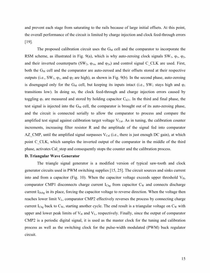
The proposed 0.5 µm CMOS (AMI) current-sensing and current-mode DC-DC buck
converter circuit was fabricated, tested, and evaluated. The power stage, the passive components
of the frequency compensation circuit, and the soft-start capacitor were off-chip (Fig. 12). The
power stage consisted of a 3.9 µH power inductor with a 48 mΩ ESR, 47 µF output capacitor,
and IRF7317 power switches having typical turn-on resistances of 65 mΩ and 27 mΩ for the
PMOS and NMOS switches, respectively. The frequency-compensating passives consisted of 15
kΩ, 1 kΩ, and 2 kΩ resistors for Ra, Rb, and Rc and 20 nF for Cz. A 2 nF capacitor was used for
the soft-start function (CSS). The rest of the circuit, as pictured in Fig. 15, was fully integrated
into a 3 mm x 1.5 mm silicon die. To accelerate the calibration phase, the digital core was
designed to disconnect GM-C filter capacitor C only during this period, but this turned out to
have adverse effects because noise degraded the calibration accuracy. An external RC low pass
filter was consequently added to the output of the GM-C filter, which was pinned out and
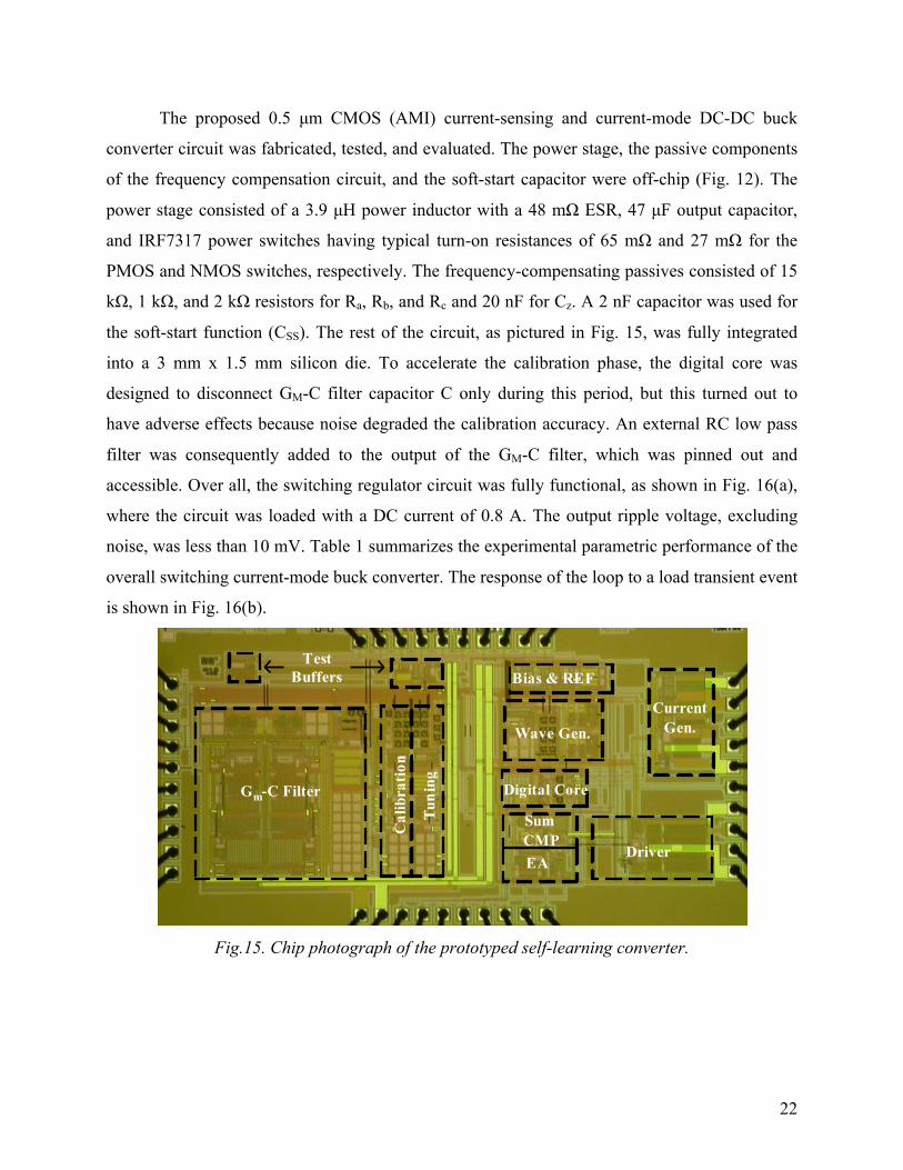
accessible. Over all, the switching regulator circuit was fully functional, as shown in Fig. 16(a),
where the circuit was loaded with a DC current of 0.8 A. The output ripple voltage, excluding
noise, was less than 10 mV. Table 1 summarizes the experimental parametric performance of the
overall switching current-mode buck converter. The response of the loop to a load transient event
is shown in Fig. 16(b).
Gm-C Filter
Tuni
ng
Cal
ibra
tion
TestBuffers Bias & REF
Wave Gen.
Digital Core
EA
SumCMP
Driver
CurrentGen.
Fig.15. Chip photograph of the prototyped self-learning converter.
23
Vo (Buck Output)
VPh (Phase Node)
Load Current -0.1 A
-0.8 A
(a)
(b)
Vo (Buck Output)
t: 2ms/divCh1: 20mV
Fig. 16. Switching converter output voltage Vo and switching node VPh waveforms under
a (a) DC load of 0.8 A and (b) output voltage under a series of transient load steps.
Table 1. Experimental parametric performance of the current-mode buck converter.
Parameter Value
Feedback Control Current-Mode Synchronous PWM
Input Voltage (Vin) 2.6 - 3.5 V Output Voltage (targeted for 1.5 V) 1.496 V
Output Current 0 - 0.8 A Switching Frequency 780 kHz
Steady-State Output Voltage Ripple < ± 10 mV Efficiency at ILoad = 0.8 A & Vin = 2.7 V
with Lossless Current Sensing with RSense Current Sensing
85.67 % 83.05 %
Load Regulation (LDR) (ILoad=0-0.8 A) -0.34 % Line Regulation (LNR) (Vin=2.7-3.5 V) 0.85 %
Soft-Start Delay 2.2 ms
24
To evaluate the ac-gain accuracy of the current-sensing circuit, a sense resistor of 50 mΩ
and a differential sense amplifier with a gain of ten was added to the printed-circuit board (PCB)
to generate a reference signal (ideal) against which the output of the proposed circuit could be
evaluated, matching the current-to-voltage gain of the circuit at 0.5 V/A. The DC accuracy was
tested against the load current to which the supply circuit was exposed. In the end, after allowing
the circuit to properly start, the measured output of the GM-C filter (i.e., sensed inductor current)
was evaluated against its ideal ac and DC counterparts (Figs. 17 and 18). The experimental
continuous inductor ripple current response of the proposed circuit matched the ac reference with
an ac error of less than 9%. The experimental DC accuracy was better than 8%, and this resulted
because the GM cell’s gain was not perfectly linear throughout the load-current range.
Vph
VSense
VRsense
(Vpp=107 mV)
(Vpp=118 mV)
Fig. 17. Experimental sensed and reference ac inductor currents.
-100
0
100
200
300
400
500
0 0.2 0.4 0.6 0.8Input Current (A)
Out
put V
olta
ge (m
V)
Ideal 0.5V/A
Calibrated for 0.5V/A
8% Error
8% Error
Fig. 18. Experimental sensed and ideal DC inductor currents.

25
As the circuit enters the tuning phase, the external LC network is first charged with a
constant current until the output voltage is raised above 1 V, at which point the test current
circuit starts sourcing a triangular current into L, as shown in Figs. 19(a) and 19(b), where the
ringing effects of rectangular waveform Vph (phase node) are the result of the parasitic
inductances and capacitances present at that node. The amplitude of the ripple is then slowly
increased from its lowest ac-gain setting (low amplitude ripple in Fig. 19(c)) until its target value
is reached (higher amplitude ripple in Fig. 19(d)), when the circuit is tuned. At this point, signal
Tune_stop is asserted eight times to alert the digital core that tuning is completed.
(c) (d)
(a)
SW1SW1
VSense
VSense
Tune_stopTune_stop
Wave Gen. Output
VTest
VPh
1.12V
(b)
Vout
nRST
Iconstcharging
ITriangulartcharging
Fig. 19. Tuning waveforms: (a) initial output voltage ramp-up, (b) steady-state triangular test-signal and phase-node waveforms, and current-sensing filter and tuning circuit outputs (c) as ripple gain is increased (before reaching its target value) and (d) after target gain is reached
and circuit is locked (tuned).
To test the tuning range of the proposed circuit, a 200 kHz, 50% duty-cycle pulse was
injected into the GM-C filter with a magnitude varying from 60 mV to 340 mV, emulating the
26
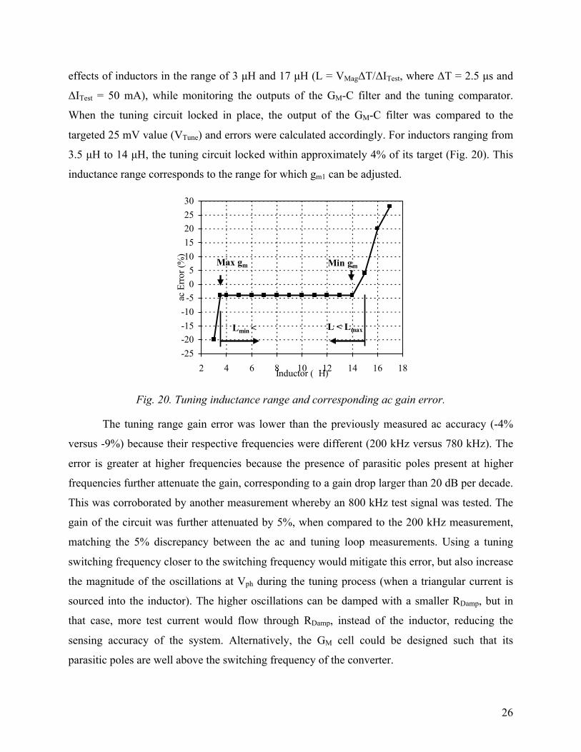
effects of inductors in the range of 3 µH and 17 µH (L = VMagΔT/ΔITest, where ΔT = 2.5 µs and
ΔITest = 50 mA), while monitoring the outputs of the GM-C filter and the tuning comparator.
When the tuning circuit locked in place, the output of the GM-C filter was compared to the
targeted 25 mV value (VTune) and errors were calculated accordingly. For inductors ranging from
3.5 µH to 14 µH, the tuning circuit locked within approximately 4% of its target (Fig. 20). This
inductance range corresponds to the range for which gm1 can be adjusted.
-25-20-15-10-505
1015202530
2 4 6 8 10 12 14 16 18Inductor (��� H)
ac E
rror (
%)
Max gm Min gm
Lmin < L
L < Lmax
Fig. 20. Tuning inductance range and corresponding ac gain error.
The tuning range gain error was lower than the previously measured ac accuracy (-4%
versus -9%) because their respective frequencies were different (200 kHz versus 780 kHz). The
error is greater at higher frequencies because the presence of parasitic poles present at higher
frequencies further attenuate the gain, corresponding to a gain drop larger than 20 dB per decade.
This was corroborated by another measurement whereby an 800 kHz test signal was tested. The
gain of the circuit was further attenuated by 5%, when compared to the 200 kHz measurement,
matching the 5% discrepancy between the ac and tuning loop measurements. Using a tuning
switching frequency closer to the switching frequency would mitigate this error, but also increase
the magnitude of the oscillations at Vph during the tuning process (when a triangular current is
sourced into the inductor). The higher oscillations can be damped with a smaller RDamp, but in
that case, more test current would flow through RDamp, instead of the inductor, reducing the
sensing accuracy of the system. Alternatively, the GM cell could be designed such that its
parasitic poles are well above the switching frequency of the converter.

27
As described in Section III, the calibration process is comprised of three phases, the first
two of which are for auto-zeroing offsets and the last is to sample the output and calibrate it
against a target value in a sequential search fashion. Fig. 21 illustrates the relevant calibration
waveforms where Phase 3 is used to process the calibration procedure, which is to stop the
calibration counter from incrementing R and the DC gain of the filter in each successive cycle
when pre-amplifier voltage VPreamp reaches its target value of 0.5 V below 1.35 V, which
corresponds to a current-sensing gain of 0.5 V/A. In testing the calibration range, the inductor’s
ESR must be considered and, for this test, a DC voltage was superimposed across the inputs of
the GM cell to emulate the DC voltage across the inductor and its ESR during start-up (VL =
RESRITest). Higher ESR values correspond to higher test voltages across the inductor during
calibration, which eases the input-offset requirements of the GM cell and therefore improves
calibration accuracy. Calibration accuracy consequently improves with higher ESR values, as
also experimentally verified (Fig. 22). The area enclosed by the solid dark lines in Fig. 22
denotes the programmability range of the GM-C filter and the gray area the region for which
there is less than 5.5% error. The end result was that ESR values below 48 mΩ (VL is 2.4 mV)
rapidly degraded the calibration accuracy (DC error) beyond 5.4% (e.g., 12% and 27% for ESRs
of 44 mΩ and 26 mΩ, respectively). Ultimately, the total gain error of the sensing circuit (ac and
DC) is the linear sum of the ac and DC errors, which amount to 8.5% for an inductance and ESR
combination of 3.9 µH and 48 mΩ at a DC load current of 0.8 A and ripple peak-to-peak current
of 0.2 A.
VSense
VPreamp
SW1
1.35V? V=20×GFilter×? VL-DC
1.35V
Phase 1Phase 2
Phase 3
Fig. 21. VPreamp and VSense during calibration, where DC filter gain GFilter is 6.38, inductor-ESR
voltage VL-DC is 3.6 mV, and supply voltage VDD is 3.2 V.

28
0
5
10
15
20
0 100 200 300 400ESR (m��� )
Indu
ctor
(���H
)
Err=1.3%
Err=1.7%Err=12%Err=27%
Err=1.9%Err=5.4%
Err=2.6%
High Error
Low-Error Tune & Calibraton Range
Gm-C Filter Range
Fig. 22. Calibration range and DC errors for increasing ESR and inductance values.
The overall efficiency performance of the current-mode DC-DC converter with and
without the current-sensing circuit for loads ranging from 0 to 0.8 A is shown in Fig. 23. In the
latter case, where a 50 mΩ series resistor is used in place of the proposed sensing circuit, the
tuning and calibration circuits and the GM-C filter were disabled and the voltage across the series
sense resistor was buffered and applied to the summing comparator, in place of VSense.
Ultimately, the sense resistor essentially incurred an efficiency loss of 2.3% at 0.8 A, which
corresponds to the gain in efficiency of the proposed scheme, when considering the accuracies
both of these schemes can achieve. As is normally the case, efficiency decreases slightly when
load currents increase beyond their mid-range level (0.5 A in this case) because of increasing
conduction losses across the power MOSFET switches.
0
10
20
30
4050
60
70
80
90
0 0.1 0.2 0.3 0.4 0.5 0.6 0.7 0.8Load Current (A)
Effic
ienc
y (%
)
R
ProposedTechnique
Vin = 2.7 V, Vo = 1.5 V
50 m���Sense
Fig. 23. Overall power efficiency of the switching power supply with the proposed current-
sensing circuit and without it (with RSense).

29
The efficiency is low during light loading conditions because the switching frequency is
constant (i.e., converter is always in PWM mode) and no power-saving scheme, such as pulse
frequency modulation (PFM), is used to decrease the frequency and therefore decrease its
associated switching power losses. In fact, a meaningful efficiency comparison cannot really be
ascertained at lighter loads (less than 0.2 A) because the design of the differential amplifier used
to amplify the voltage across the sense resistor is not optimized and its quiescent power losses
are higher than those of the GM-C filter prototyped. The efficiency at these lighter loads is
expected to be on the same order because, just as the amplifier amplifies the voltage across the
sense resistor, the GM-C filter processes the voltage across the inductor, both of which constitute
constant loads to the system. Table 2 summarizes the experimental parametric performance of
the proposed self-learning current-sensing CMOS circuit prototype and its GM-C filter.
The tuning and calibration functions of the proposed current-sensing GM-C filter can be
viably implemented with a digital-signal processor (DSP), but only if a high quality analog
reference is used to calibrate the current-sensing device, or if the analog test-signal and tuning
and calibration method proposed here are used. Digital controllers for high speed applications,
however, are often less appealing than their analog counterparts because of their relatively higher
silicon real-estate demands, longer response times (lower speed), and higher processing costs
[29], and a DSP is therefore not always available. State-of-the-art analog current-sensing
solutions, on the other hand, such as a Sense-FET, may be less accurate and only applicable to
on-chip switches but often less complex and less area-intensive, and they should consequently be
used in crude on-chip current-sensing applications. The proposed technique is accurate and
lossless but relatively complex, so its market space tends to be in high performance applications
where current-based mode-hopping schemes are used to increase efficiency and improve
regulating performance.
The relatively long calibration and tuning cycles can be considerably reduced if the
sequential search (i.e., linear search with a sequential up counter) were replaced with a binary
search (i.e., successive range divisions) or any other more sophisticated convergent search
algorithm. For instance, while a linear search requires an average of 2N-1 counts, where N is the
number of programmability bits, the binary search only requires N, thereby potentially
decreasing the 500 ms calibration process down to approximately 16 ms. Alternatively, if time
overhead is still an issue, the long calibration cycles can be altogether avoided during soft re-start

30
events by deglitching the events and storing the calibration settings in on-chip memory modules;
the settings could then be refreshed and reprogrammed during hard re-set conditions.
Table 2. Experimental parametric performance of the proposed self-learning current-sensing CMOS circuit prototype.
Parameter Value Technology AMI’s CMOS 0.5 µm Die Area (including pads) 3 mm x 1.5 mm Quiescent Current for Entire System (during normal operation)
1.6 - 2.1 mA (for various values of gm1)
Input Supply Voltage 2.6 - 3.5 V Self-Learning Current-Sensing Circuit
Load Current (Inductor DC Current) 0 - 0.8 A Sensing Gain (Rgain=VSense/IL) 0.5 V/A Errors (ILoad=0.8 A, ΔIL=0.2 A) ac DC (including offsets) Random Offset Non Linearity (Systematic Offset) Total (weighted DC + ac errors)
-9% +8%
±0.4% -2%
8.51% Tunable Inductor Range 3.5 µH -14 µH Inductor’s ESR Range 48 mΩ – 384 mΩ Worst-Case Start-Up Time 484 ms
GM-C Filter BW (1/RC) Programmability (worst-case resolution by design)
1.1 kHz to 6.4 kHz (3.2%)
Gain (gmR) Programmability (worst-case resolution by design)
1.27 - 29.16 (V/V) (3.2%)
Input-Referred Offset for 3 Samples at Gain=9.92, Max. R, VDD=3-4.2V, and ICMR=1-1.5 V
< ±210 µV
Transient Glitches < 40 mV Input-Referred Total Noise (C=60 pF, Gain=9.92, & Max. R) 93 µV
Filter Nonlinearity (Δgm/gm) For a Rail-to-Rail Input (3 V) -57 dB
Second (Parasitic) Pole 4 MHz Auto-Zeroing Clock Frequency 1 kHz
For considerably higher switching frequency applications (e.g., 100 MHz), the
bandwidths of the GM-C cell, controller, and all signal-processing blocks must be scaled
accordingly, and the switching noise that is injected as a result is similarly filtered. The
underlying idea behind the proposed current-sensing scheme is to build a voltage-mode GM-C

31
filter that reproduces the filtering effects the inductor has on its current, so its respective
bandwidths are equal to RESR/2πL, which is relatively low compared to the switching frequency
(e.g., a few kHz of bandwidth compared to a few MHz of switching frequency). Consequently,
the switching noise injected into the analog filter is well attenuated (e.g., by about 60 dB),
making the foregoing solution relatively robust to switching noise. Although switching
frequencies on the order of hundreds of mega-Hertz are attractive from the perspective of LC
integration, practical designs generally conform to lower switching frequencies (e.g., less than 10
MHz) to keep switching power losses low and therefore maintain high efficiency performance.
The 200 MHz converter reported in [30] achieved 80% efficiency in part because its input supply
voltage was 1.2 V and switching losses were consequently significantly lower, which would not
have been the case in a Li-Ion-supplied application (2.7 - 4.2 V) where switching losses would
have been drastically increased (proportional to the square of the supply voltage).
VI. Conclusions
A fully integrated continuous, lossless, and accurate self-learning current-sensing 0.5 µm
CMOS circuit was presented, and along with a current-mode switching buck DC-DC converter
platform, designed, fabricated, and experimentally tested. Its overall sensing accuracy was 8.5%
for a tunable inductor and ESR range of 3.5 µH - 14 µH and 48 mΩ - 384 mΩ, when state-of-
the-art lossless and fully integrated solutions achieve between 20% and 40% only when knowing
the power inductor’s inductance. The driving novelty behind the system is its accurate self-
learning feature, wherein the voltage gain and bandwidth of an on-chip GM-C filter are
automatically matched to the power inductor’s current frequency response during power-on-reset
events to emulate the inductor current and indirectly measure the off chip power inductor’s
inductance and ESR. Even though the technique was only applied to a peak current-mode
switching buck converter, the scheme extends to most inductor-based switching regulator
topologies, such as boost and buck-boost converters, independent of the current ratings of the
power stage and whether on- or off-chip power switches are used. The self-learning current-
sensing feature proposed affords the designer the flexibility required to address emerging state-
of-the-art challenges by allowing the power supply system to self-adjust and mode-hop
according to its passive and active loading conditions, in the process optimizing speed and power

32
efficiency performance, which are more critical than ever today, especially in portable, battery-
powered applications.
ACKNOWLEDGEMENT
The authors would like to especially thank John Seitters from Intersil Corporation and
Todd Harrison from Texas Instruments for their valuable comments and general support, as well
as MOSIS for fabricating the CMOS prototype chip, and the reviewers for their valuable
feedback.
REFERENCES
[1] G. A. Rincón-Mora, Power Management ICs – A Top-Down Design Approach. New York, NY: Lulu, 2005.
[2] P. Krein, Elements of Power Electronics. New York, NY: Oxford University Press, 1998.
[3] N. A. Keskar and G. A. Rincón-Mora, “Self-stabilizing, integrated, hysteretic boost DC-DC converter,” in Proc. 2004 IEEE Industrial Electronics Conference (IECON), pp. TA3-4.
[4] M. Gildersleeve, H. P. Forghani-zadeh, and G. A. Rincón-Mora, “A comprehensive power analysis and a highly efficient, mode-hopping DC-DC converter,” in Proc. 2002 IEEE Asian Pacific ASIC Conference, pp. 153-156.
[5] Current-sharing techniques for VRMs, Technical Brief TB385.1, Milpitas, CA: Intersil Corporation.
[6] W. Ki, D. Ma, “Single-inductor multiple-output switching converters,” in Proc. 2001 IEEE Power Electronics Specialists Conference (PESC), pp. 226 – 231.
[7] L. A. Milner and G. A. Rincón-Mora, “A novel predictive inductor multiplier for integrated circuit DC-DC converters in portable applications,” in Proc. 2005 International Symposium on Low Power Electronics and Design (ISLPED).
[8] H. P. Forghani-zadeh and G. A. Rincón-Mora, “Current-sensing techniques for DC-DC converters,” in Proc. 2002 Midwest Symposium on Circuits and Systems (MWSCAS), pp. 577-580.
[9] R. Lenk, “Application bulletin AB-20 optimum current-sensing techniques in CPU converters,” Fairchild Semiconductor Application Notes, 1999.
[10] W. Schults, “Lossless current sensing with SENSEFET enhance the motor drive,” Motorola Technical Report, 1988.
[11] S. Yuvarajan, “Performance analysis and signal processing in a current sensing current MOSFET (SENSEFET),” in Proc. 1990 Industry Applications Society Annual Meeting, pp. 1445–1450.

33
[12] P. Givelin and M. Bafleur, “On-chip over-current and open-load detection for a power MOS high-side switch: a CMOS current-source approach,” in Proc. 1993 European Conference on Power Electronics and Applications, pp. 197 –200.
[13] S. Yuvarajan and L. Wang, “Power conversion and control using a current-sensing MOSEFET,” in Proc. 1992 Midwest Symposium on Circuits and Systems (MWSCAS), pp.166 –169.
[14] J. Chen, J. Su, H. Lin, C. Chang, Y. Lee, T. Chen, H. Wang, K. Chang, and P. Lin, “Integrated current sensing circuits suitable for step-down DC-DC converters,” Electronics Letters, Feb. 2004, pp. 200-201.
[15] C. Lee and P. Mok, “A monolithic current-mode CMOS DC-DC converter with on-chip current-sensing technique,” IEEE Journal of Solid States Circuits, vol. 39, Jan. 2004, pp. 3-14.
[16] P. Drennan and C. McAndrew, “Understanding MOSFET mismatch for analog design,” IEEE Journal of Solid States Circuits, vol. 38, Mar. 2003, pp. 450-459.
[17] E. Dallago, M. Passoni, and G. Sassone, “Lossless current-sensing in low-voltage high-current DC-DC modular supplies,” IEEE Trans. on Industrial Electronics, vol. 47, Dec. 2000, pp. 1249-1252.
[18] H. P. Forghani-zadeh and G. A. Rincón-Mora, “A lossless, accurate, self-calibrating current-sensing technique for DC-DC converters,” in Proc. 2005 Industrial Electronics Conference (IECON), pp. 549 - 554.
[19] C. Enz and G. Temes, “Circuit technique for reducing the effects of circuit imperfections,” Proceedings of IEEE, pp. 1586-1614, Nov. 1996.
[20] H. P. Forghani-zadeh and G. A. Rincón-Mora, “A continuous, low-glitch, low-offset, programmable gain and bandwidth gm-C filter,” in Proc. 2005 Midwest Symposium on Circuits and Systems (MWSCAS), pp. 1629-1632.
[21] C. Toumazou, J. Lidgey, and D. Haigh, Analogue IC Design: the Current-Mode Approach, Peter Peregrinus Ltd: London, UK, 1990.
[22] K. Koli, CMOS Current Amplifiers: Speed versus Nonlinearity, PhD dissertation, Helsinki University of Technology, 2000.
[23] H. Elwan, A. Soliman, “Low-voltage low-power CMOS current conveyors,” IEEE Transaction on Circuits and Systems-I (TCAS I), vol., pp. 828-835, Sept. 1997.
[24] R. Poujois and J. Borel, “A low-drift fully integrated operational amplifier,” IEEE Journal of Solid State Circuits, vol. 13, pp. 499-505, Aug. 1978.
[25] C. Reis Filho and A. Santiago, “CMOS building blocks for smart-power integrated circuits,” in Proc. 1996 International Conference on Electronics, Circuits, and Systems (ICECS), pp. 892-896.
[26] R. Middlebrook, “Modeling current-programmed buck and boost regulators,” IEEE Transactions on Power Electronics, vol. 4, Jan. 1989, pp. 36-52.
[27] P. Allen and D. Holberg, CMOS Analog Circuit Design, Oxford, NY: Oxford university press, 2002.

34
[28] R. Gregorian, Introduction to CMOS Op-Amps and Comparators. New York, NY: Wiley, 1999.
[29] B. Patella, A. Prodic, A. Zirger, and D. Maksimovic, "High-frequency digital PWM controller IC for DC-DC converters," IEEE Transactions on Power Electronics, January 2003, vol. 18, issue 1, part 2, pp. 438-446.
[30] P. Hazucha, et al., “A 233-MHz 80%-87% efficient four-phase DC-DC converter utilizing air-core inductors on package,” IEEE J. Solid States Circuits, Vol. 40, April 2005, pp. 838 – 845.


![A Low Voltage, Dynamic, Non-inverting, …users.ece.gatech.edu › rincon › publicat › jrnls › pe03_bck-bst.pdfdischarged [1]. Therefore, systems designed for a nominal supply](https://img.pdfslide.us/doc/110x75/5f1080697e708231d4496c4f/a-low-voltage-dynamic-non-inverting-usersece-a-rincon-a-publicat-a-jrnls.jpg)


![A High Efficiency, Linear RF Power Amplifier With a Power ...users.ece.gatech.edu/rincon/publicat/jrnls/mtts03_pa_dyn.pdfDoherty amplifier for extended power range [4] has been demonstrated](https://img.pdfslide.us/doc/110x75/61489f672918e2056c22cec3/a-high-efficiency-linear-rf-power-amplifier-with-a-power-usersece-doherty.jpg)