Embed Size (px)
Citation preview

www.ams.com Revision 1.2 / 21/02/2014 page 1/13
AS3993
Radon Demo Reader – Hardware Description
Application Note: Radon Demo Reader – HW Description

Radon Demo Reader
Hardware Description
www.ams.com Revision 1.2 / 21/02/2014 page 2/13
Table of Contents
1 General Description ............................................................................................................. 3
1.1 Kit Content ........................................................................................................................... 4
2 Getting Started ..................................................................................................................... 4
3 Hardware Description........................................................................................................... 5
3.1 RF Circuit ............................................................................................................................. 5
3.2 Power Supply ....................................................................................................................... 6
3.3 MCU ..................................................................................................................................... 7
3.3.1 Bootloader ............................................................................................................................ 8
3.4 FW Programming ................................................................................................................. 8
3.5 UART ................................................................................................................................... 9
3.6 Measurement & Test Points ................................................................................................. 9
3.6.1 DC Voltages: ........................................................................................................................ 9
3.6.2 Signal Test Points .............................................................................................................. 10
3.6.2.1 OAD & OAD2 ..................................................................................................................... 10
3.6.3 SPI Interface Signals.......................................................................................................... 10
3.6.4 RF Test Points ................................................................................................................... 11
3.6.5 Antenna Connections ......................................................................................................... 12
4 Software Description .......................................................................................................... 12
Copyright ........................................................................................................................................... 13
Disclaimer .......................................................................................................................................... 13
Figure 1 - Connecting the Radon Reader ........................................................................................... 4
Figure 2 - AS3993 Reader Suite - Main Window ................................................................................ 5
Figure 3 - LED Error Codes ................................................................................................................. 7
Figure 4 - Connecting the ICD3 Programmer ..................................................................................... 8
Figure 5 - Debug Interface Pinout ....................................................................................................... 8
Figure 6 - UART Interface Pinout ........................................................................................................ 9
Figure 7 – DC Testpoint Connector Pinout ....................................................................................... 10
Figure 8 - Signal Testpoint Pinout ..................................................................................................... 10
Figure 9 - Locating the SPI Interface Connector ............................................................................... 10
Figure 10 - SPI Interface Connector Pinout ...................................................................................... 11
Figure 11 - RF Testpoint Adapter (not included in the demo kit) ...................................................... 11
Figure 12 - RF Test Point Description ............................................................................................... 12
Figure 13 - SMB Plug (Female) ......................................................................................................... 12

Radon Demo Reader
Hardware Description
www.ams.com Revision 1.2 / 21/02/2014 page 3/13
Revision History
Revision Date Owner Description
1.0 Dec 2013 bhi Initial Document
1.1 Feb 2014 bhi Corrections
1.2 Feb 2014 bhi Corrections and Information added
1 General Description
The Radon is an EPC Class 1 Gen 2 UHF RFID reader system with the purpose of demonstrating
the AS3993 IC in a high power reader application for long read ranges.
The Radon is operated through a graphical user interface (GUI) running on a host computer which
implements tag inventory and tag access routines. It also facilitates full access to the AS3993 IC
registers allowing the user to configure and optimize the reader for various use cases and is used
for updating the firmware of the Radon reader. The host computer communicates with the Radon
reader via USB interface.
The Radon is powered by an external 5V DC supply as well as by the USB interface. The USB
interface supplies the MCU and all digital tunable capacitors. Therefore it is possible to program the
MCU without connecting the external 5V DC Supply. The external 5V DC powers the AS3993, the
pre-amplifier, the power amplifier and the LNA.
The AS3993 IC is controlled via the SPI interface by a PIC24 MCU which can be disconnected1 in
order to allow other MCU types to control the AS3993. The RF signal is generated by a PLL/VCO
circuitry integrated in the AS3993 IC. As a frequency reference a 20 MHz TCXO is used. The RF
signal is output at the differential low power outputs RFONX and RFOPX. After the Balun (2:1) the
RF signal is attenuated by a resistive, discrete attenuator in order to limit the input power for the
external pre-amplifier to follow. After the pre-amplifier stage the RF signal is amplified by a power
amplifier and filtered by a ceramic low pass filter and a ceramic high pass filter in order to limit
harmonics and spurious frequencies introduced by the various gain stages. To isolate the TX signal
from the differential mixer input of the AS3993 IC a directional 10 dB coupler is used. At the input
coupled port of the directional coupler a tuning circuitry is placed which allows controlled impedance
adjustments in order to suppress TX leakage reaching the AS3993 receiver. At the direct output of
the directional coupler a RF switch is placed which allows routing the RF signal to one of the two
antenna ports. For antenna port 1 only, an additional tuning circuit is placed which allows adaptive
impedance matching in case the antenna properties (S11) are poor for a given frequency.
The incoming RX signal is coupled to the differential RX mixer input of AS3993 via a 2:1 balun. The
optional LNA stage on the receive side is bypassed per default but is otherwise fully operational and
can be connect through a solder change.
The Radon reader PCB is placed inside an enclosure with a metallic base which is acting as a heat
sink and a plastic cover. The plastic cover is held by magnets and can be lifted to allow access the
PCB. The PCB is mounted by four screws to the metallic base. Underneath the PA an adhesive
1 By desoldering zero ohm resistors

Radon Demo Reader
Hardware Description
www.ams.com Revision 1.2 / 21/02/2014 page 4/13
heat conducting tape is placed. In case the PCB needs to be removed from the metallic base it is
recommend to heat up the metallic base first in order to prevent any damages to the PCB by
bending the PCB.
1.1 Kit Content
Every AS3993 Radon Demo Kit contains:
1 x AS3993 Radon Reader
1 x 5V power supply (without IEC-60320 C13 cable)
1 x Micro USB cable
2 x SMA/SMB coax antenna cable
1 x USB thumb drive with documentation
1 x Tag demo bag
2 Getting Started
The following step-by-step instructions describe how to connect the hardware correctly and how to
operate the GUI to scan for tags:
1) Connect the antenna to antenna port 2 (J7)
2) Connect the 5V DC power cable to the DC jack (P1)
3) Connect the Radon reader to the host computer using the Micro USB cable.
4) At this point the MCU LED (D13) is flashing and the Antenna 2 LED (D11) is permanently
on.
Figure 1 - Connecting the Radon Reader
5) Start the AS3993 Reader Suite on the host computer.
6) The Radon reader is listed in the main window and the state shows Online in green letters.
7) To scan2 for tag click on the Start Scan button in the lower left corner of the main window.
2 Adhere to local RF regulations.

Radon Demo Reader
Hardware Description
www.ams.com Revision 1.2 / 21/02/2014 page 5/13
Figure 2 - AS3993 Reader Suite - Main Window
3 Hardware Description
This section describes in detail the circuitry of the Radon reader and outlines important
measurement points as well as easy modification options.
3.1 RF Circuit
The RF signal is generated by the integrated PLL/VCO circuit inside AS3993. The reference
frequency is provided by an external 20 MHz TCXO with a clipped sine wave output wave form and
an amplitude of 0.8Vpp. The TCXO is supplied by a regulated 3.3V voltage generated by an ultra-
low noise LDO (AS1362). The output of the TCXO is connected to OSCO (pin 30) of AS3993 via a
1 nF capacitor. The output of the internal PLL- charge pump is connected to LF_CEXT (pin 45) at
which the external part of the loop filter is closely placed. An additional low pass filter stage is
integrated in AS3993 and is part of the loop filter circuit. The loop filter output is the control voltage
of the internal VCO.
The RF signal is output at the differential low power outputs (pin 23, 24) which have a differential
output impedance of 100 Ohms. The default output level of the Radon reader is approx.. -6 dBm
which is controlled by register 0x15 of AS3993. The output stage is supplied via VDD_B (pin 12). 39
nH inductors block the RF signal from reaching VDD_B while two blocking capacitors block the DC
voltage towards the Balun. The Balun has a balanced impedance of 100 ohms and an unbalanced
impedance of 50 ohms. The insertion loss of the Balun is ~1dB.
To limit the input power for the external pre-amplifier a discrete resistive attenuator is placed after
the Balun. The attenuator has an attenuation of 7dB and an input/output impedance of 49 ohms.
The pre-amplifier (SGC2363Z) increases the RF power to approx. 1.8 dBm. The pre-amplifier has a
dedicated regulated voltage (AS1362) supply of 3.3V.

Radon Demo Reader
Hardware Description
www.ams.com Revision 1.2 / 21/02/2014 page 6/13
The RF power is further amplified by an external PA (RF6886) to ~1W depending on the output
frequency. Radon outputs at 915 MHz per default 30 dBm. For ETSI frequencies the output power
is 25 dBm. The amplifier stages of the PA are supplied by 3.6V from a dedicated LDO (LT1764)
which provides enough current for the PA stage. The bias voltages for the two stages are
connected to VDD_PA (pin 13) of AS3993 which is set to 3V (register 0x0B).
After the PA stage two filters are placed which attenuate higher frequency harmonics and spurious
frequencies generated by the amplifier stages. The high pass filter stage shows at 860 MHz an
insertion loss of approx. 1dB. At 740 MHz the filter has 3dB of attenuation. The low pass filter has at
1 GHz an insertion loss below 1dB. The low pass filter has ~45dB attenuation a 1.8GHz and
2.4GHz.
The filtered RF signal is then connected to the directional coupler which isolates the TX signal from
the differential mixer inputs of the AS3993 IC. The directional coupler has a coupling factor of 10dB
and an isolation of 25 dB (typically).
At the input coupled port a tuning circuit (system tuner) with variable impedance is connected. This
allows adaptively improving the virtual directivity of the coupling device. The tuning circuitry
comprises of three digitally adjustable capacitors (PE64904) and discrete components. The digital
capacitors are controlled via SPI by the MCU.
To the output of the directional coupler a RF switch is connected which routes the RF signal to one
of the two antenna ports.
Between the RF switch and the antenna port 1 an additional antenna tuning circuit is available
which allows matching the antenna impedance to the reader system. The antenna matching circuit
comprises of two digitally adjustable capacitors and discrete components.
To the isolated output of the directional coupler a Balun is connected which transforms the singled-
ended RF signal to a differential one. The differential RF signal is connected to the mixer inputs (pin
4, 6) of AS3993. For experimental use a LNA is placed which can increase the sensitivity of the
reader in case the tag responses have a low signal level and the reflected power is optimized by the
system tuner. The LNA circuitry is bypassed per default but can be included by re-soldering C97
and C99.
3.2 Power Supply
The Radon reader is externally powered by a 5V DC source. The inner contact of the connector is
positive. From this voltage all other voltages for the analog part are generated through LDOs. The
MCU is supplied by a regulated voltage (AS1364) derived from the USB interface which allows to
programming the MCU without the DC power supply.
The pre-amplifier and the AS3993 are supplied by a fixed output voltage (3.3V) version of AS1362.
The LDO output voltage for the PA is adjustable and is set to 3.6V.
(
)
(
)

Radon Demo Reader
Hardware Description
www.ams.com Revision 1.2 / 21/02/2014 page 7/13
3.3 MCU
The MCU used for the Radon is a PIC24FJ64GB004 type in a 44 pin TQFP package. The
communication between the MCU and the host computer is done via the USB interface. A UART
firmware version is also available. The UART interface needs to be connected to J5. The square pin
indicated pin 1 of J5 and is connected to the TX pin of the controller. Pin 2 corresponds to RX and
pin 3 is connected to digital GND. The MCU is clocked by a 12 MHz crystal. The MCU controls the
AS3993 IC and the digital tunable capacitors used in the tuning circuits via the SPI. The MCU is
also controlling the 6 LEDs on the Radon.
D10 (Tag Read) - RA4 (pin 34):
Flashes upon a tag read.
D9 (RF ON) - RP4 (pin 33):
Illuminated if the RF power is switched ON.
D8 (Untuned) - RA8 (pin 32):
Indicates that the reflected power is too high and tuning the reader systems is
recommended.
D13 (MCU) - RP6 (pin 20):
MCU is idle. During scanning for tags the LED remains in its current state (bright or dark).
D7 (Antenna 1) – RA9 (pin 35):
Illuminated if the RF power is switched to the Antenna Port 1 (J14)
D11 (Antenna 2) – RP22 (pin 2):
Illuminated if the RF power is switched to the Antenna Port 2 (J7)
During the reader start-up a self-check is performed. In case an error occurs, the LEDs D13, D8
and D9 binary encode the source of the error by being permanently active.
Error Code #
Active LED
Description
1 MCU SPI Error on MISO MOSI, CLK or NCS
2 Untuned EN line failed
3 MUC, Untuned
IRQ line failed
4 RF ON Crystal not stable
5 MCU, RF ON
PLL not locked
Figure 3 - LED Error Codes
The Button accessible on the outside of the housing allows resetting the controller.
In case the USB is connected before the external DC supply the controller immediately starts with
self-check. But at this point the AS3993 is not yet supplied. An error message is display in the GUI.
Radon Demo Reader
Hardware Description
www.ams.com Revision 1.2 / 21/02/2014 page 8/13
To recover from this state click OK to remove the error message an press the reset button or
reconnect the USB connector.
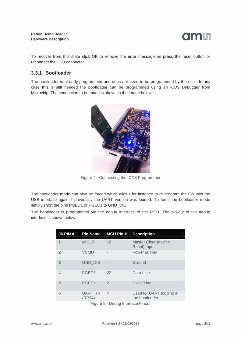
3.3.1 Bootloader
The bootloader is already programmed and does not need to be programmed by the user. In any
case this is still needed the bootloader can be programmed using an ICD3 Debugger from
Microchip. The connection to be made is shown in the image below:
Figure 4 - Connecting the ICD3 Programmer
The bootloader mode can also be forced which allows for instance to re-program the FW with the
USB interface again if previously the UART version was loaded. To force the bootloader mode
simply short the pins PGED1 or PGEC1 to GND_DIG.
The bootloader is programmed via the debug interface of the MCU. The pin-out of the debug
interface is shown below:
J6 PIN # Pin Name MCU Pin # Description
1 /MCLR 18 Master Clear (device Reset) Input.
2 VCMU - Power supply
3 GND_DIG - Ground
4 PGED1 22 Data Line
5 PGEC1 21 Clock Line
6 UART_TX (RP24)
4 Used for UART logging in the bootloader
Figure 5 - Debug Interface Pinout

Radon Demo Reader
Hardware Description
www.ams.com Revision 1.2 / 21/02/2014 page 9/13
3.4 FW Programming
A new firmware version can be programmed using AS3993 Reader Suite via the Help menu. For
more instruction please refer to the User Manual of the AS3993 Reader Suite. For programming
only the USB interface needs to be connected.
3.5 UART
In order to operate the reader through the UART interface the TX and RX lines should be connected
to J5. It is recommended to use a FTDI USB/TTL Serial Cable (TTL-232R-3V3)
J5 PIN # Pin Name MCU Pin # Note
1 (square)
UART_TX 4 Connect with RXD (yellow) of TTL-232R-3V3
2 UART_RX 5 Connect with TXD (orange) of TTL-232R-3V3
3 GND_DIG - GND
Figure 6 - UART Interface Pinout
The UART connection settings are:
Baud Rate: 115.2 kbps
Data bits: 8
Parity: None
Stop Bits: 1
Handshaking: none
3.6 Measurement & Test Points
The Radon has numerous measurement points built in which allows checking various important
voltages, analog and digital signal lines.
3.6.1 DC Voltages:
Important voltages can be measured at the following test points. Please note that the voltages
VAPC and VMIX are valid only during scanning for tags.
Testpoint Pin # Description
J1 J1-1 VUSB, 5V from USB
J1-2 5V from DC jack
J17 J17-1 VPA
J17-2 GND
J11 J11-1- VEXT

Radon Demo Reader
Hardware Description
www.ams.com Revision 1.2 / 21/02/2014 page 10/13
J11-2 GND
J20 J20-1 VAPC
J20-2 GND
J19 J19-1 VLNA
J19-2 GND
J12 J12-1 VMIX
J12-2 GND
Figure 7 – DC Testpoint Connector Pinout
3.6.2 Signal Test Points
Testpoint Pin # Description
J21 J21-1 OAD
J21-2 GND
J22 J22-1 OAD2
J22-2 GND
J16
J16-1- SW_ANT
J16-2 GND
J12-2 GND
Figure 8 - Signal Testpoint Pinout
3.6.2.1 OAD & OAD2
The OAD and OAD2 signals are very useful for debugging purposes or subsequent signal
processing. Through register settings (0x10) it is possible to output
Analog or digitized I, Q subcarrier signals
TX modulation and selected subcarrier. Observe reader commands and tag responses.
Analog Mixer DC output to determine the self-jamming level.
3.6.3 SPI Interface Signals
On J10, J26 and J27 AS3993 signal lines and the SPI signals can be monitored.
Figure 9 - Locating the SPI Interface Connector

Radon Demo Reader
Hardware Description
www.ams.com Revision 1.2 / 21/02/2014 page 11/13
Pin # Description
J10-1 (square)
SPI_CLK
J10-2 GND_DIG
J10-3 GND_DIG
J10-4 GND_DIG
J10-5 GND_DIG
J26-1 AS3993_EN
J26-2 AS3993_IRQ
J26-3 SPI_NCS
J26-4 SPI_MISO
J26-5 SPI_MOSI
J27-1 (square)
SPI_SEN: Enable Antenna DTC 2
J27-2 SPI_SEN: Enable Antenna DTC 1
J27-3 SPI_SEN: Enable System DTC 1
J27-4 SPI_SEN: Enable System DTC 2
J27-5 SPI_SEN: Enable System DTC 3
Figure 10 - SPI Interface Connector Pinout
If it is required to control the Radon through an external MCU it is possible to unsolder the resistors
R10 – R18 which disconnects the existing PIC24 MCU. This is sometimes beneficial and saves time
as the firmware development can start early. R10 – R18 are located on the backside of the Radon
PCB.
3.6.4 RF Test Points
The Radon reader allows measuring the RF power at various points. The RF tracks can be
contacted through subminiature coax sockets with a built in switch. It is recommended to use
matching connection adapters which are available from Hirose. For example a SMA conversion
adapter MS-156-HRMJ-2
Figure 11 - RF Testpoint Adapter (not included in the demo kit)
If the adapter is connected to the coax socket the RF track on the PCB is disconnected. Please
note that the coax sockets have limited plug/unplug cycles of 500 times.
Pin # Description
P6 Single ended AS3993 output power after the external attenuator.
P5 Pre-amplifier output power

Radon Demo Reader
Hardware Description
www.ams.com Revision 1.2 / 21/02/2014 page 12/13
P8 PA output power
P11 Impedance of system tuning circuit
P3 RF power at the receiver (single-ended) for measuring the tag responses and self-jammer level.
P4 LNA output.
Figure 12 - RF Test Point Description
3.6.5 Antenna Connections
Radon reader has two antenna connection ports while the antenna ports slightly differ. For Antenna
Port 1 an antenna tuning circuit is available which allows tuning the connected antenna
independently from the tuning of the system tuner. The draw-back of this antenna port is the
additional insertion loss introduced by the antenna tuning circuit. Antenna Port 2 does not have an
antenna tuning circuit. The antenna socket is of SMB type.
Note: Some SMB cables, when plugged-in for the first time, might be slightly difficult to mate with
the connector on the Radon board. Place the SMB plug absolutely straight above the jack and try to
connect with a fair amount of pressure. Excessive pressure might damage the GND cage inside the
cable plug.
!
Figure 13 - SMB Plug (Female)
4 Software Description
Please refer to the User Manual for a more information on the AS3993 Reader Suite.
Caution!
The Radon reader is intended for engineering usage to demonstrate the AS3993.
Before turning the Radon reader ON please check your local RF regulations and
configure the reader accordingly.
Always connect a RF load to the antenna port in use,

Radon Demo Reader
Hardware Description
www.ams.com Revision 1.2 / 21/02/2014 page 13/13
The Radon demo reader PCB is mounted into a metallic enclosure which acts as a
heat sink and therefore tends to get hot.
Do not touch the hot metallic enclosure after prolonged operation of the reader with
the RF field set to high power.
Copyright
Copyright © 1997-2014, ams AG, Tobelbader Strasse 30, 8141 Unterpremstaetten, Austria-Europe. Trademarks Registered ®. All rights reserved. The material herein may not be reproduced, adapted, merged, translated, stored, or used without the prior written consent of the copyright owner. All products and companies mentioned are trademarks or registered trademarks of their respective companies.
Disclaimer
Devices sold by ams AG are covered by the warranty and patent indemnification provisions appearing in its Term of Sale. ams AG makes no warranty, express, statutory, implied, or by description regarding the information set forth herein or regarding the freedom of the described devices from patent infringement. ams AG reserves the right to change specifications and prices at any time and without notice. Therefore, prior to designing this product into a system, it is necessary to check with ams AG for current information. This product is intended for use in normal commercial applications. Applications requiring extended temperature range, unusual environmental requirements, or high reliability applications, such as military, medical life-support or lifesustaining equipment are specifically not recommended without additional processing by ams AG for each application. For shipments of less than 100 parts the manufacturing flow might show deviations from the standard production flow, such as test flow or test location. The information furnished here by ams AG is believed to be correct and accurate. However, ams AG shall not be liable to recipient or any third party for any damages, including but not limited to personal injury, property damage, loss of profits, loss of use, interruption of business or indirect, special, incidental or consequential damages, of any kind, in connection with or arising out of the furnishing, performance or use of the technical data herein. No obligation or liability to recipient or any third party shall arise or flow out of ams AG rendering of technical or other services.
Contact Information
Headquarters
ams AG Tobelbader Strasse 30 8141 Unterpremstaetten Austria T. +43 (0) 3136 500 0 For Sales Offices, Distributors and Representatives, please visit: http://www.ams.com/contact