Embed Size (px)
DESCRIPTION
Amplifiers
Citation preview

Prepared Under the guidance of,Mr. H V ravish Aradhya,
Asst. Professor,Dept. of ECE,
RVCE, Bengaluru
AMPLIFIERS

Introduction to amplifiersTo amplify AC or DC signalAmplitude levelDevices used: FET, OP-AMP, transistor, etc..Communication systems.Design to provide desired output voltage by designing
for desired gain.VO/Vi
Types of gain:Amount of amplification depends on FEEDBACK
NETWORK.Feedback:Types of feedback:
Positive feedback AmplifiersNegative feedback (Regenerative circuits, (Oscillators)

CLASSIFICATION OF AMPLIFIERSClassified based on
Based on its input:
Based on its output:
Based on its frequency range:
Based on biasing conditions:
Based on transistor configurations:

DECIBELSIts convenient to measure the power in logarithmic
scale rather than linear graph.(2 – 3)W, (10 – 11)W (Ratios: 50% and
11.1%)Ratio determines change in loudness.Power Gain = Log(Ratio of output to input)belsActual unit is dB, 1/10th of bel = 10xLog(Ratio of
output to input)PO = Power dissipating through RL and
Pi = Power dissipating through input resistance Ri
P = V2/RP = i2R
PROBLEMSThe output power from an amplifier is 50W when
the signal frequency is 5KHz. The power falls to 25mW when the frequency is increased to 20KHz. Calculate the output power change in dB.
Advantages of representing gain in dB
Overall gain = Product of individual gains.Here addition of individual gains in dB.Very small and very large value can be
represented considerably by using small figures.0.0000001 = -140dB and 100000 = 100dB.

HALF POWER POINTSConsider frequency response of an amplifierAmplifier will not amplify frequency components
equally.If amplification is not equal, output will be
distorted frequency distortion.Max gain over a range of frequenciesReduced gain below and above.
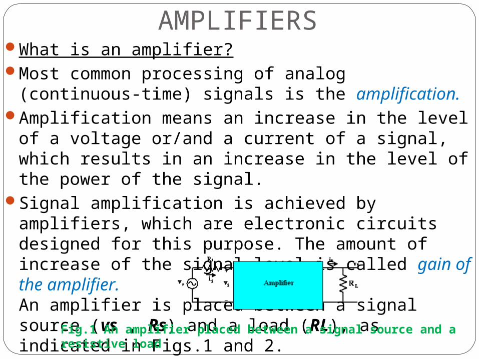
AMPLIFIERSWhat is an amplifier?Most common processing of analog (continuous-
time) signals is the amplification. Amplification means an increase in the level of a
voltage or/and a current of a signal, which results in an increase in the level of the power of the signal.
Signal amplification is achieved by amplifiers, which are electronic circuits designed for this purpose. The amount of increase of the signal level is called gain of the amplifier. An amplifier is placed between a signal source (vs , Rs) and a load (RL), as indicated in Figs.1 and 2.
Fig.1 An amplifier placed between a signal source and a resistive load

The input of the amplifier is driven by a signal from the signal source and delivers the amplified signal to the load.
At least one active element e.g. a transistor, is necessary in order to obtain a simple, one stage amplifier, (Fig.2).
Fig. 2 Single-stage amplifier between a signal source and a resistive load
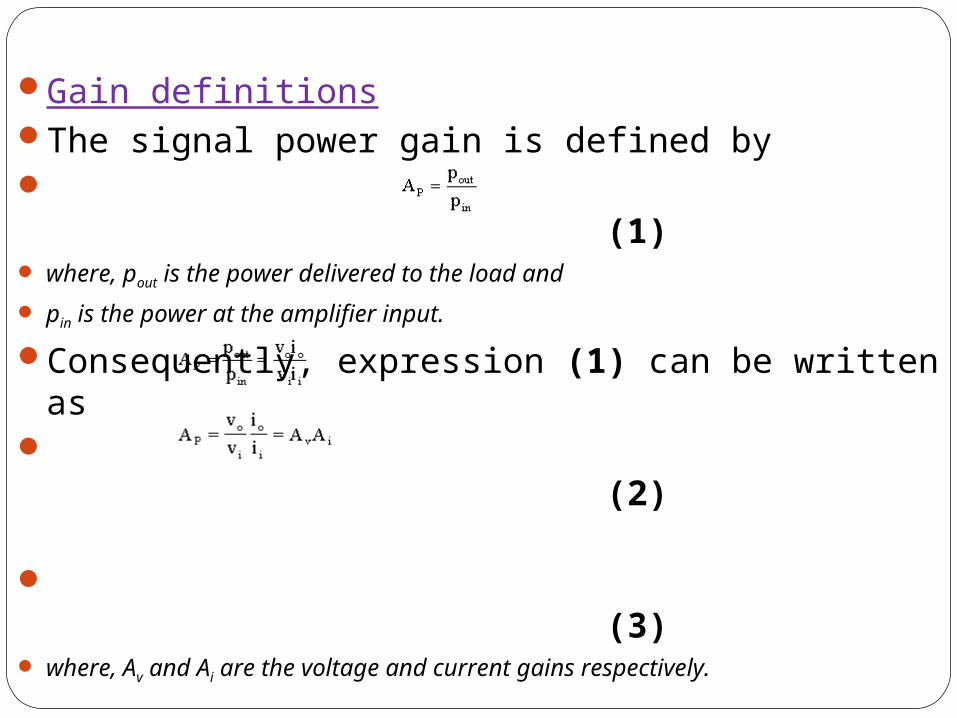
Gain definitions The signal power gain is defined by (1) where, pout is the power delivered to the load and
pin is the power at the amplifier input.
Consequently, expression (1) can be written as (2)
(3) where, Av and Ai are the voltage and current gains respectively.
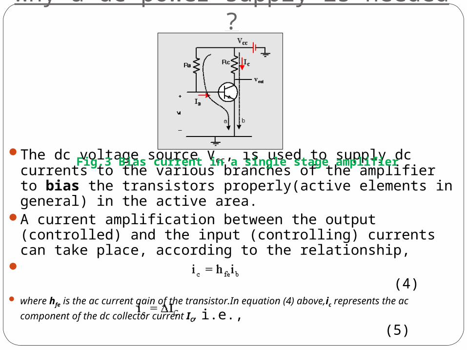
Why a dc power supply is needed ?
The dc voltage source Vcc, is used to supply dc currents to the various branches of the amplifier to bias the transistors properly(active elements in general) in the active area.
A current amplification between the output (controlled) and the input (controlling) currents can take place, according to the relationship,
(4)
where hfe is the ac current gain of the transistor.In equation (4) above,ic represents
the ac component of the dc collector current IC, i.e., (5)
Fig.3 Bias current in a single stage amplifier
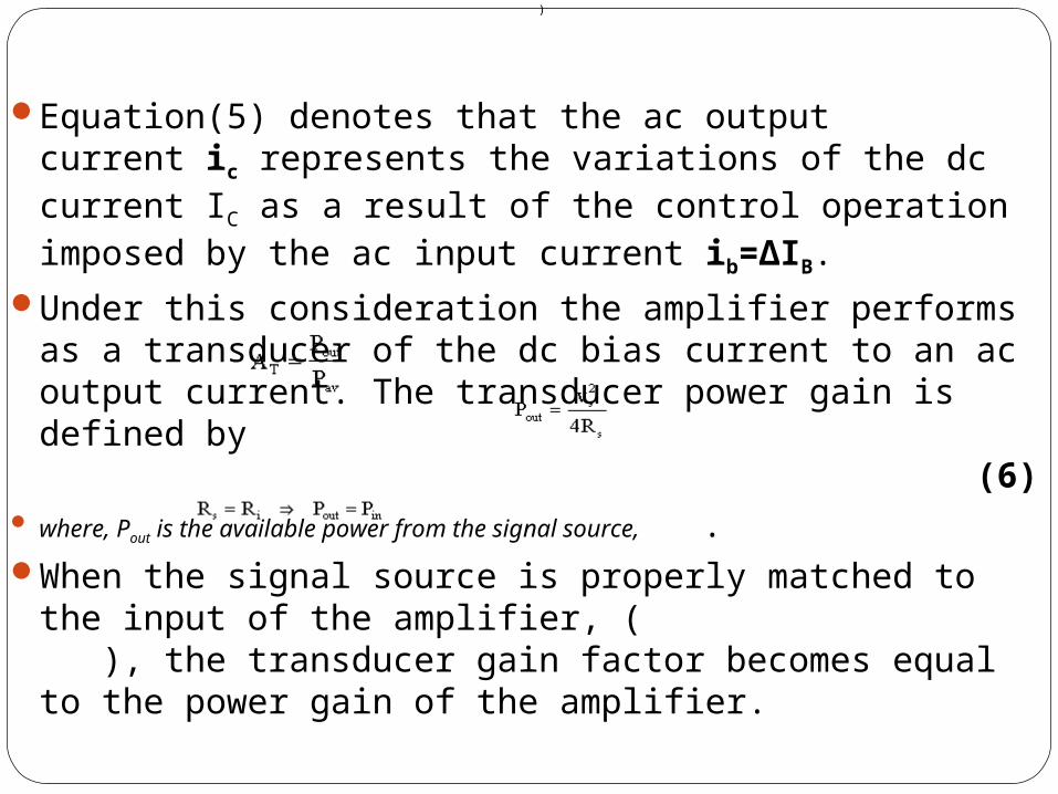
Equation(5) denotes that the ac output current ic represents the variations of the dc current IC as a result of the control operation imposed by the ac input current ib=ΔIB.
Under this consideration the amplifier performs as a transducer of the dc bias current to an ac output current. The transducer power gain is defined by (6)
where, Pout is the available power from the signal source, . When the signal source is properly matched to the
input of the amplifier, ( ), the transducer gain factor becomes equal to the power gain of the amplifier.
)

Stages of an amplifier The gain required from an amplifier is higher than
we can obtain with a single stage amplifier. In such a case, several stages of amplification are
cascaded to obtain the desired result, (multistage amplifiers).
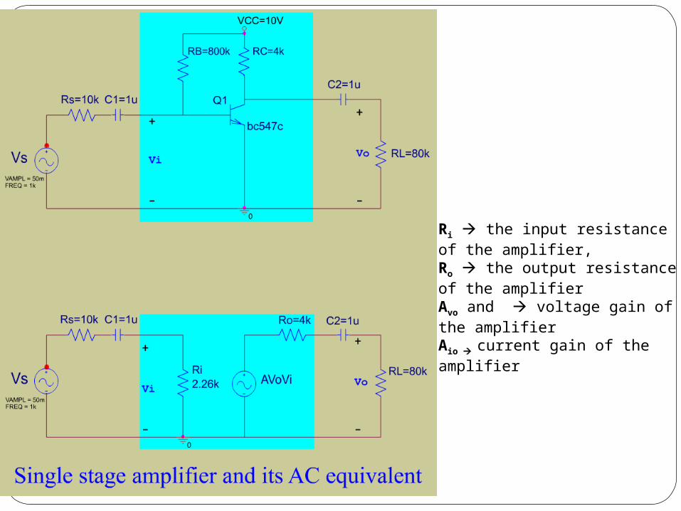
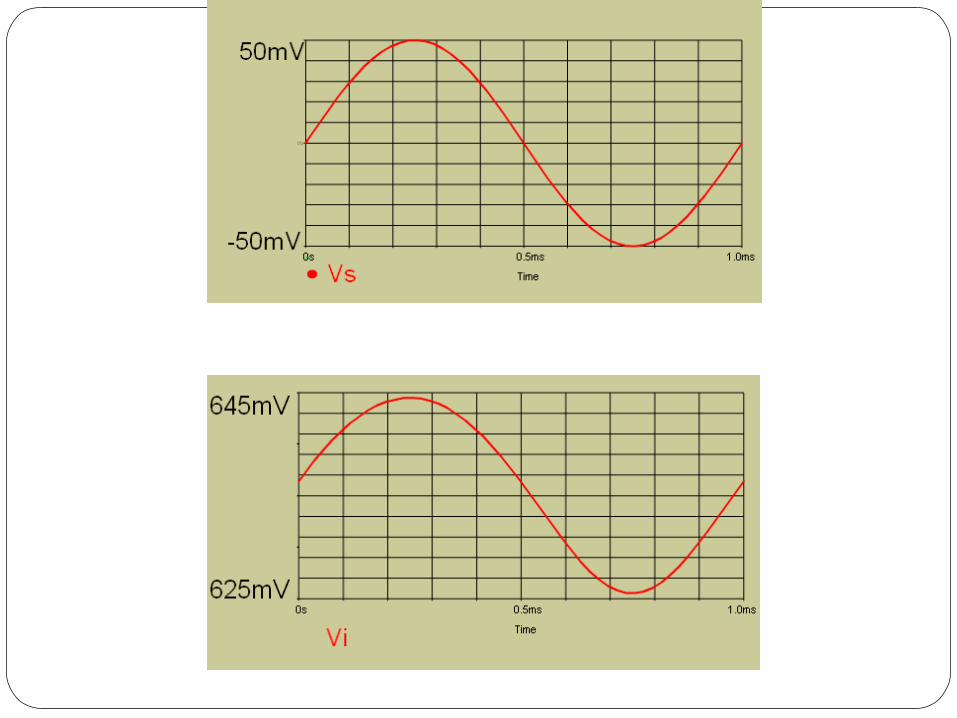
Ri the input resistance of the amplifier, Ro the output resistance of the amplifier Avo and voltage gain of the amplifierAio current gain of the amplifier

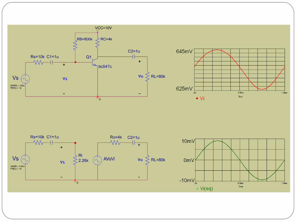
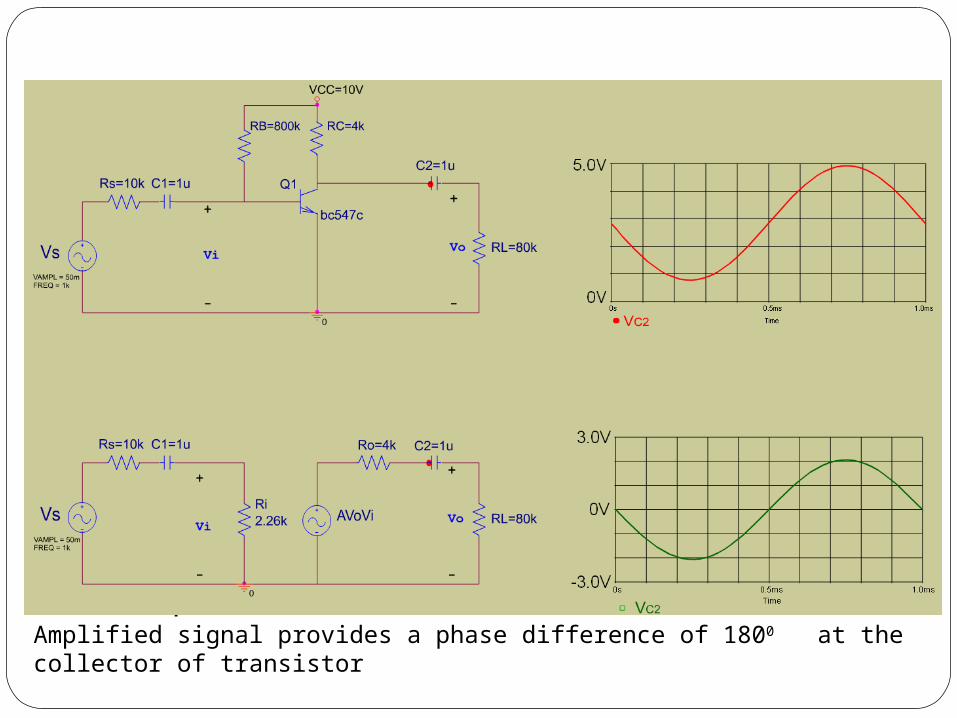
Amplified Amplified signal provides a phase difference of 1800 at the collector of transistor


CE amplifiers are very popular to amplify the small signal ac
After a transistor has been biased with a Q point near the middle of a dc load line, ac source can be coupled to the base.
This produces fluctuations in the base current and hence in the collector current of the same shape and frequency.
The output will be enlarged sine wave of same frequency.The amplifier is called linear if it does not change the
wave shape of the signal. As long as the input signal is small, the transistor will use
only a small part of the load line and the operation will be linear.
On the other hand, if the input signal is too large, the fluctuations along the load line will drive the transistor into either saturation or cut off.
This clips the peaks of the input and the amplifier is no longer linear.

The coupling capacitor (CC ) passes an ac signal from one point to another.
Coupling Capacitorblocks dc to pass through it. Hence it is also called blocking capacitor.
the ac voltage at point A is transmitted to point B.For this series reactance XC should be very small
compared to series resistance RS
As frequency increases, decreases, and current increases until it reaches to its maximum value vin / R
The size of the coupling capacitor depends upon the lowest frequency to be coupled
for lowest frequency XC < 0.1R is taken as design rule.

The coupling capacitor acts like a switch, which is open to dc and shorted for ac.
The bypass capacitor Cb is similar to a coupling capacitor, except that it couples an ungrounded point to a grounded point
The Cb capacitor looks like a short to an ac signal and therefore emitter is said ac grounded
A bypass capacitor does not disturb the dc voltage at emitter because it looks open to dc current.
As a design rule XCb < 0.1RE at lowest frequency.
Analysis of CE amplifier:the dc source sets up quiescent current and
voltages. The ac source then produces fluctuations in these
current and voltages.The simplest way to analyze this circuit is to split
the analysis in two parts: dc analysis and ac analysis.
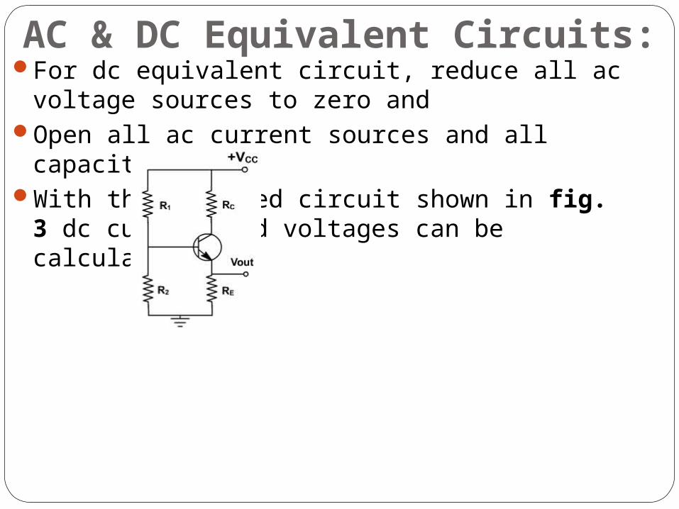
AC & DC Equivalent Circuits:For dc equivalent circuit, reduce all ac voltage
sources to zero and Open all ac current sources and all capacitors. With this reduced circuit shown in fig. 3 dc current
and voltages can be calculated.
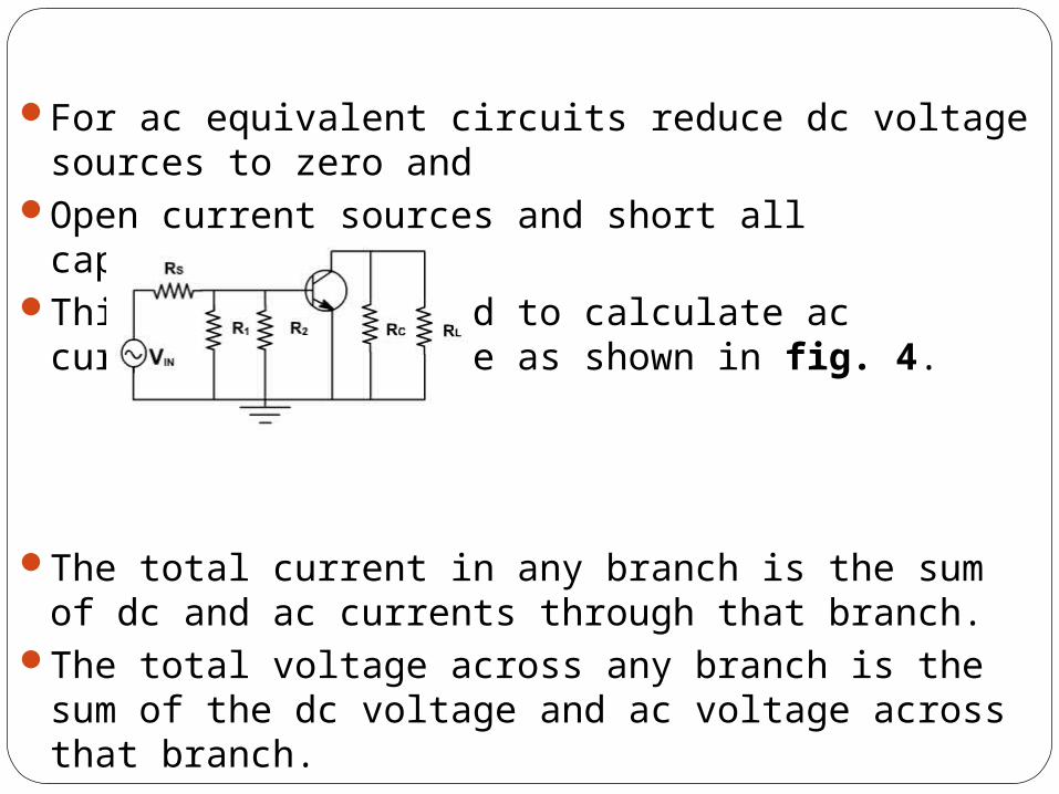
For ac equivalent circuits reduce dc voltage sources to zero and
Open current sources and short all capacitors. This circuit is used to calculate ac currents and
voltage as shown in fig. 4.
The total current in any branch is the sum of dc and ac currents through that branch.
The total voltage across any branch is the sum of the dc voltage and ac voltage across that branch.

Phase Inversion:Because of the fluctuation is base current; collector current
and collector voltage also swings above and below the quiescent voltage.
The ac output voltage is inverted with respect to the ac input voltage, meaning it is 180o out of phase with input.
During the positive half cycle base current increase, causing the collector current to increase.
This produces a large voltage drop across the collector resistor; therefore,
the voltage output decreases and negative half cycle of output voltage is obtained.
on the negative half cycle of input voltage less collector current flows and the voltage drop across the collector resistor decreases, and hence
collector voltage increases we get the positive half cycle of output voltage as shown in fig. 5.
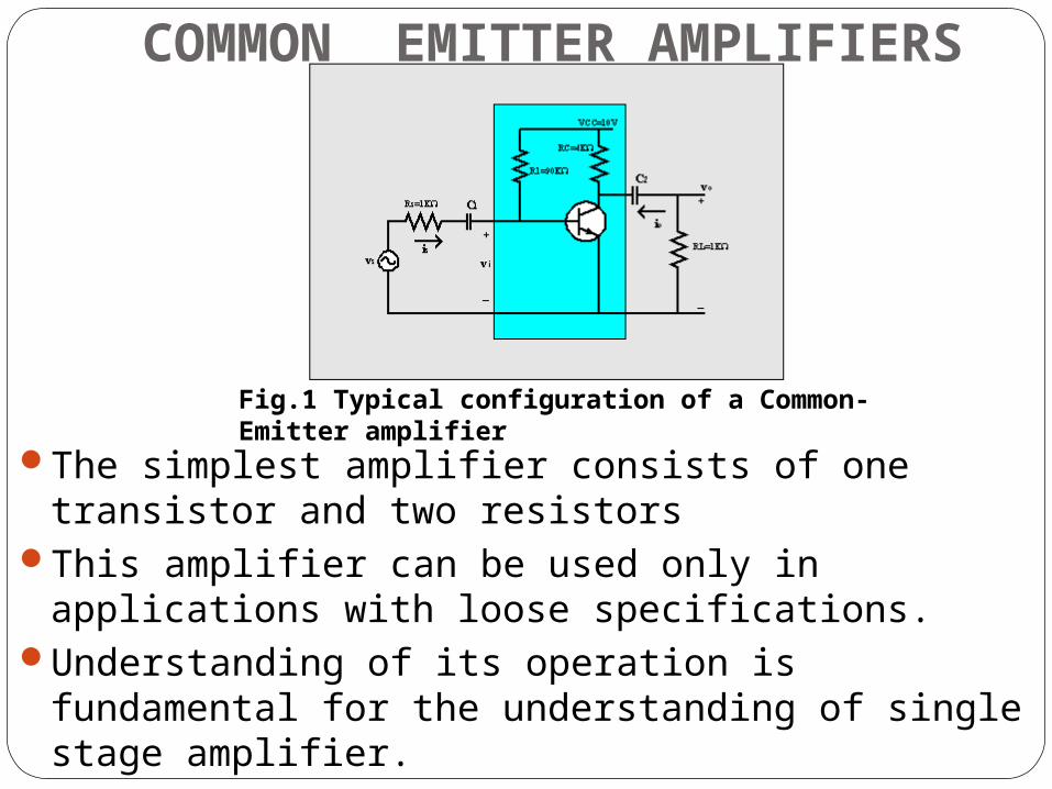
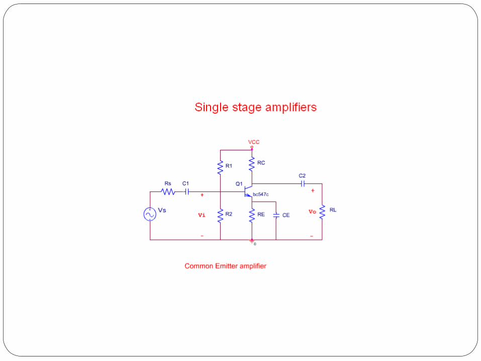
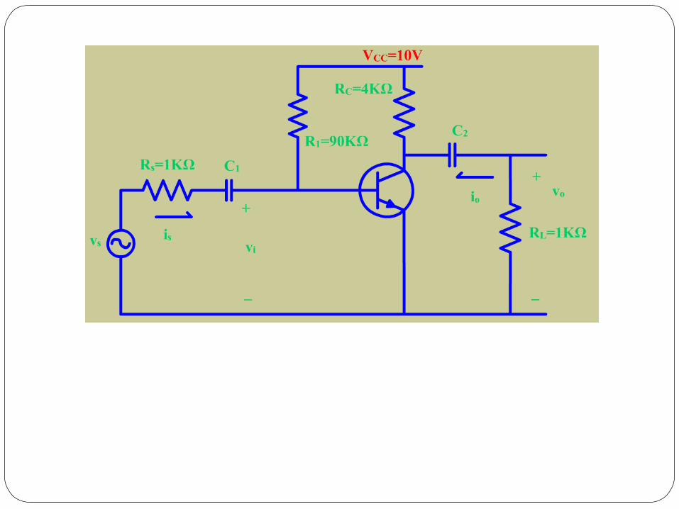
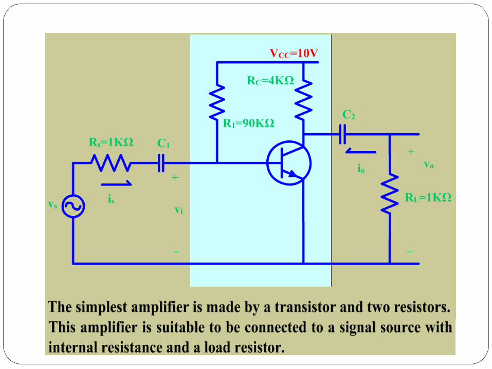
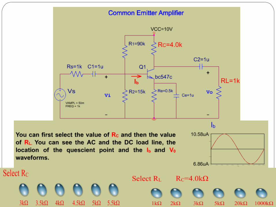
COMMON EMITTER AMPLIFIERS
The simplest amplifier consists of one transistor and two resistors
This amplifier can be used only in applications with loose specifications.
Understanding of its operation is fundamental for the understanding of single stage amplifier.
Fig.1 Typical configuration of a Common-Emitter amplifier
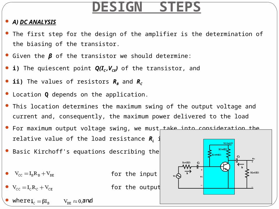
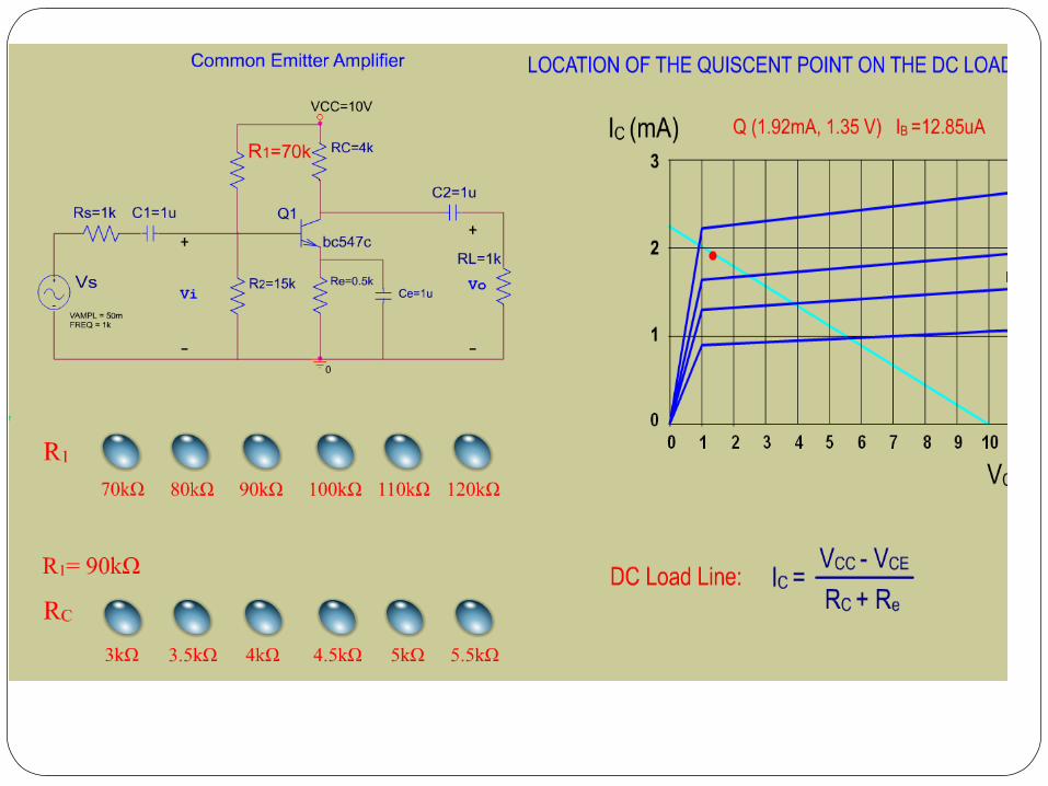
DESIGN STEPS A) DC ANALYSIS
The first step for the design of the amplifier is the determination of the biasing of the
transistor.
Given the β of the transistor we should determine:
i) The quiescent point Q(IC ,VCE) of the transistor, and
ii) The values of resistors RB and RC
Location Q depends on the application.
This location determines the maximum swing of the output voltage and current and,
consequently, the maximum power delivered to the load
For maximum output voltage swing, we must take into consideration the relative
value of the load resistance RL in comparison to the value of RC
Basic Kirchoff's equations describing the circuit
for the input circuit
for the output circuit
where, and for a Si transistor

Rules of thump for locating the quiescent point Q for almost symmetrical output clipping
CASE A: RL>>RC
We set (VCE=5.2 V)
(IC=1.25 mA)Consequently, the bias point Q is located
at (IC=1,25mA, VCE=5.2V)

the maximum output voltage swing is,
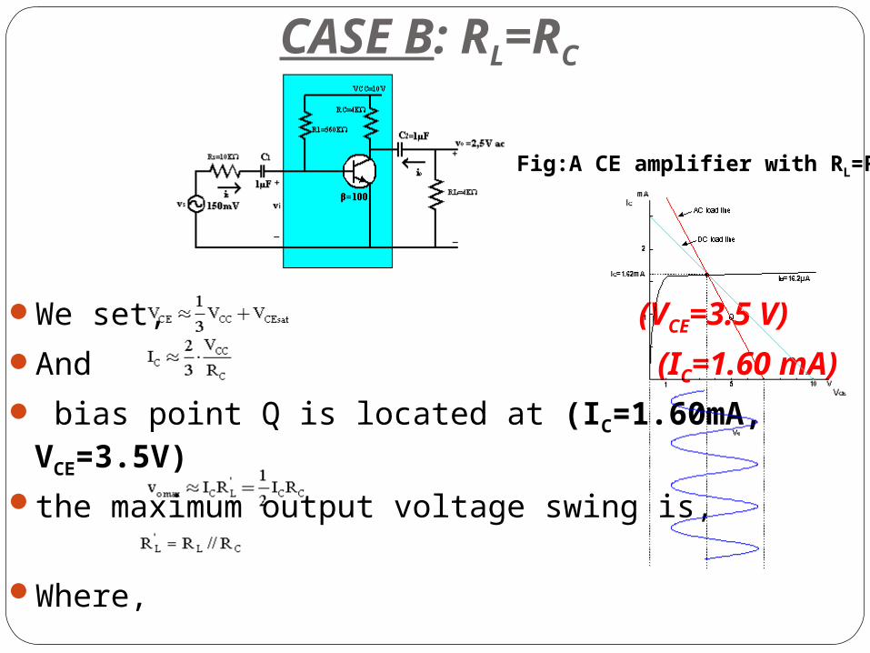
CASE B: RL=RC
We set, (VCE=3.5 V)
And (IC=1.60 mA)
bias point Q is located at (IC=1.60mA, VCE=3.5V)the maximum output voltage swing is,
Where,
Fig:A CE amplifier with RL=RC
CASE C: RL<<RCthe amplifier operates as a voltage controlled
current amplifier, (transconductance amplifier) and thus,
maximum output voltage swing is of no interest.
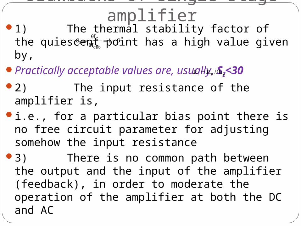
Drawbacks of single stage amplifier
1) The thermal stability factor of the quiescent point has a high value given by,
Practically acceptable values are, usually, SI<302) The input resistance of the amplifier is,i.e., for a particular bias point there is no free
circuit parameter for adjusting somehow the input resistance
3) There is no common path between the output and the input of the amplifier (feedback), in order to moderate the operation of the amplifier at both the DC and AC


CALCULATION OF Q-POINT
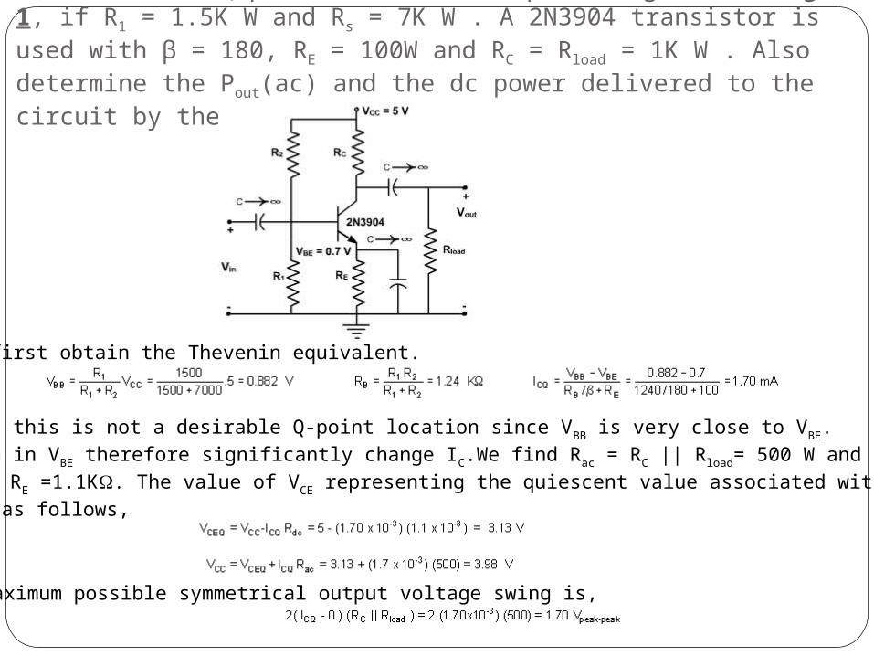
Determine the Q-point for the CE amplifier given in fig. 1, if R1 = 1.5K W and Rs = 7K W . A 2N3904 transistor is used with β = 180, RE = 100W and RC = Rload = 1K W . Also determine the Pout(ac) and the dc power delivered to the circuit by the source.
We first obtain the Thevenin equivalent.
Note that this is not a desirable Q-point location since VBB is very close to VBE.
Variation in VBE therefore significantly change IC.We find Rac = RC || Rload= 500 W and
Rdc = RC + RE =1.1K. The value of VCE representing the quiescent value associated with ICQ
is found as follows,
the maximum possible symmetrical output voltage swing is,
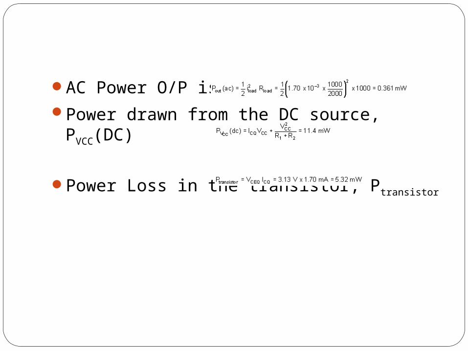
AC Power O/P is PAC
Power drawn from the DC source, PVCC(DC)
Power Loss in the transistor, Ptransistor


