Embed Size (px)
Citation preview

SOLOMON SYSTECH SEMICONDUCTOR TECHNICAL DATA
This document contains information on a new product. Specifications and information herein are subject to change without notice. http://www.solomon-systech.com SSD1332 Rev 1.6 P 1/56 June 2005 Copyright 2005 Solomon Systech Limited
Advance Information
96RGB x 64 Dot Matrix OLED/PLED Segment/Common Driver with Controller
SSD1332

SSD1332 Rev 1.6 P 2/56 June 2005 Solomon Systech
TABLE OF CONTENTS
1 GERENAL INFORMATIOM ........................................................................................................................6
2 FEATURES......................................................................................................................................................6
3 ORDERING INFORMATION.......................................................................................................................6
4 BLOCK DIAGRAM........................................................................................................................................7
5 SSD1332Z GOLD BUMP DIE PAD ASSIGNMENT...................................................................................8
6 PIN DESCRIPTION......................................................................................................................................13 BS0, BS1, BS2.........................................................................................................................................................13 CS# ..........................................................................................................................................................................13 RES#........................................................................................................................................................................13 D/C ..........................................................................................................................................................................13 R/W(WR#) ..............................................................................................................................................................13 E (RD#) ...................................................................................................................................................................13 D7-D0 .......................................................................................................................................................................13 VDD ..........................................................................................................................................................................14 VSS ...........................................................................................................................................................................14 VCC...........................................................................................................................................................................14 VREF .........................................................................................................................................................................14 VPA, VPB, VPC ............................................................................................................................................................14 IREF ...........................................................................................................................................................................14 VCOMH ......................................................................................................................................................................14 COM0-COM63........................................................................................................................................................15 SA0-SA95, SB0-SB95, SC0-SC95..........................................................................................................................15
7 FUNCTIONAL BLOCK DESCRIPTIONS ................................................................................................16 OSCILLATOR CIRCUIT AND DISPLAY TIME GENERATOR...........................................................................................16 RESET CIRCUIT.........................................................................................................................................................16 COMMAND DECODER AND COMMAND INTERFACE...................................................................................................16 CURRENT AND VOLTAGE SUPPLY.............................................................................................................................17 SEGMENT DRIVERS/COMMON DRIVERS ...................................................................................................................18 MPU PARALLEL 6800-SERIES INTERFACE................................................................................................................21 MPU PARALLEL 8080-SERIES INTERFACE................................................................................................................21 MPU SERIAL INTERFACE .........................................................................................................................................21 GRAPHIC DISPLAY DATA RAM (GDDRAM) ..........................................................................................................22 GRAY SCALE AND GRAY SCALE TABLE ...................................................................................................................23 DC-DC VOLTAGE CONVERTER................................................................................................................................25
8 COMMAND TABLE.....................................................................................................................................26 DATA READ / WRITE ................................................................................................................................................30
9 COMMAND DESCRIPTIONS ....................................................................................................................31
10 GRAPHIC ACCELERATION COMMAND SET DESCRIPTION.........................................................38
11 MAXIMUM RATINGS.................................................................................................................................41
12 DC CHARACTERISTICS............................................................................................................................41

Solomon Systech June 2005 P 3/56 Rev 1.6 SSD1332
13 AC CHARACTERISTICS............................................................................................................................42
14 APPLICATION EXAMPLE ........................................................................................................................46
15 SSD1332U1R1 COF PACKAGE DIMENSIONS .......................................................................................47
16 SSD1332U1R1 COF PIN ASSIGNMENT ...................................................................................................49
17 SSD1332T1R1 TAB PACKAGE DIMENSIONS........................................................................................51
18 SSD1332T1R1 TAB PIN ASSIGNMENT....................................................................................................53
19 SSD1332Z PACKAGE DETAILS................................................................................................................55
SSD1332 Rev 1.6 P 4/56 June 2005 Solomon Systech
TABLE OF FIGURES Figure 1 - Block Diagram .............................................................................................................................. 7 Figure 2 – SSD1332Z Pin Assignment ......................................................................................................... 8 Figure 3 - SSD1332Z Alignment mark dimensions..................................................................................... 12 Figure 4 - Oscillator Circuit.......................................................................................................................... 16 Figure 5 – IREF Current Setting by Resistor Value....................................................................................... 17 Figure 6 – Segment and Common Driver Block Diagram........................................................................... 18 Figure 7 – Segment and Common Driver Signal Waveform....................................................................... 19 Figure 8 – Gray Scale Control by PWM in Segment .................................................................................. 20 Figure 9 - Display data read back procedure - insertion of dummy read.................................................... 21 Figure 10 – 65k Color Depth Graphic Display Data RAM Structure ........................................................... 22 Figure 11 – 65k Color Depth Graphic Display Data Writing Sequence ...................................................... 22 Figure 12 – 256 Color Depth Graphic Display Data RAM Structure for One Pixel..................................... 23 Figure 13 – Relation between graphic data RAM value and gray scale table entry for three colors in 65K
color mode ........................................................................................................................................... 23 Figure 14 – illustration of relation between graphic display RAM value and gray scale control................. 24 Figure 15 – DC-DC Converter Application Circuit Diagram........................................................................25 Figure 16 – Example of Column and Row Address Pointer Movement ..................................................... 31 Figure 17 – Segment Output Current for Different Contrast Control and Master Current Setting.............. 32 Figure 18 – Address Pointer Movement of Horizontal Address Increment Mode....................................... 33 Figure 19 – Address Pointer Movement of Vertical Address Increment Mode........................................... 33 Figure 20 – Example of Set Display Start Line with no Remap.................................................................. 34 Figure 21 – Example of Set Display Offset with no Remap........................................................................ 34 Figure 22 – Example of gamma correction by gray scale table setting ...................................................... 36 Figure 23 – Example of Draw Line Command............................................................................................ 38 Figure 24 – Example of Draw Rectangle Command .................................................................................. 38 Figure 25 – Example of Copy Command.................................................................................................... 39 Figure 26 – Example of Copy + Clear = Move Command ......................................................................... 40 Figure 27 - 6800-series MPU parallel interface characteristics .................................................................. 43 Figure 28 - 8080-series MPU parallel interface characteristics .................................................................. 44 Figure 29 - Serial interface characteristics.................................................................................................. 45 Figure 30 - Application Example for SSD1332U1R1 .................................................................................. 46 Figure 31 - SSD1332U1R1 COF pin assignment ....................................................................................... 49 Figure 32 - SSD1332T1R1 TAB pin assignment ........................................................................................ 53

Solomon Systech June 2005 P 5/56 Rev 1.6 SSD1332
LIST OF TABLES Table 1 - Ordering Information ...................................................................................................................... 6 Table 2 - SSD1332Z Die Pad Coordinates ................................................................................................... 9 Table 3 – MCU Interface Selection Setting................................................................................................. 13 Table 4 – Components Selection for DC-DC Converter .............................................................................25 Table 5 – Configuration Command Table ................................................................................................... 26 Table 6 – Graphic Acceleration Command Set Table ................................................................................ 29 Table 7 - Read Command Table................................................................................................................. 30 Table 8 - Address increment table (Automatic)........................................................................................... 30 Table 9 – Result of Change of Brightness by Dim Window Command ...................................................... 39 Table 10 - Maximum Ratings ...................................................................................................................... 41 Table 11 - DC Characteristics..................................................................................................................... 41 Table 12 - AC Characteristics ..................................................................................................................... 42 Table 13 - 6800-Series MPU Parallel Interface Timing Characteristics ..................................................... 43 Table 14 - 8080-Series MPU Parallel Interface Timing Characteristics ..................................................... 44 Table 15 - Serial Interface Timing Characteristics ...................................................................................... 45 Table 16 - SSD1332U1R1 COF pin assignment ........................................................................................ 50 Table 17 - SSD1332T1R1 TAB pin assignment ......................................................................................... 54

Solomon Systech June 2005 P 6/56 Rev 1.6 SSD1332
1 GERENAL INFORMATIOM
The SSD1332 is a single-chip CMOS OLED/PLED driver with controller for organic/polymer light emitting diode dot-matrix graphic display system. It consists of 288 segments (96RGB) and 64 commons. This IC is designed for Common Cathode type OLED panel.
The SSD1332 displays data directly from its internal 96x64x16 bits Graphic Data RAM (GDDRAM). Data/Commands are sent from general MCU through the hardware selectable 6800/8000 series compatible Parallel Interface or Serial Peripheral Interface. It has a 256 steps contrast control and 65K color control.
2 FEATURES ! Support max. 96RGB x 64 matrix panel ! Power supply: VDD = 2.4V - 3.5V
VCC = 7.0V - 18.0V ! OLED driving output voltage, 16V maximum ! DC-DC voltage converter ! Segment maximum source current: 200uA ! Common maximum sink current: 50mA ! Embedded 96x64x16 bit SRAM display buffer ! 16 step master current control, and 256 step current control for the three color components ! Programmable Frame Rate ! Graphic Acceleration Command Set (GAC) ! 8-bit 6800-series Parallel Interface, 8-bit 8080-series Parallel Interface, Serial Peripheral
Interface. ! Wide range of operating temperature: -40 to 85 °C
3 ORDERING INFORMATION Table 1 - Ordering Information
Ordering Part Number SEG COM Package Form Reference Remark
SSD1332U1R1 96RGB 64 COF
Page 47
• 35mm film • 5 sprocket hole • 80 / 68 / SPI interface • SEG lead pitch 0.06mm • COM lead pitch 0.09mm
SSD1332T1R1 96RGB 64 TAB
Page 52
• 35mm film • 5 sprocket hole • Folding TAB • 80 / 68 / SPI interface • SEG lead pitch 0.06mm • COM lead pitch 0.09mm
SSD1332Z 96RGB 64 COG Page 8 • Min SEG pad pitch: 41.2 µm • Min COM pad pitch: 41.2 µm

SSD1332 Rev 1.6 P 7/56 June 2005 Solomon Systech
4 BLOCK DIAGRAM
Com
mon
Driv
ers (
odd)
S
egm
ent D
river
s
C
omm
on D
river
s(ev
en)
G
rey
Scal
e D
ecod
er
D
ispl
ay
Tim
ing
Gen
erat
or
O
scill
ator
G
DD
RA
M
MC
U
Inte
rface
RES#CS#
D/C#E (RD#)
R/W#(WR#)BS2BS1BS0
D7D6D5D4D3D2D1D0
DC
-DC
vol
tage
conv
erte
r
Seg/
Com
OLE
D
Driv
ing
bloc
k
C
omm
and
Dec
oder
VDD
VSS
VC
C
VC
OM
H
VR
EF
VPA
VPB
VPC
I REF
.
.
.
.
.
.
.
.
.
.
.
.
.
.
.
.
.
.
.
.
.
.
COM62 COM60
|
COM2 COM0
SA0 SB0 SC0 SA1 SB1 SC1
|
SA95 SB95 SC95
CL
CLS
COM1 COM3
|
COM61 COM63
.
.
.
.
.
.
.
.
.
.
.
GD
RR
ESE FB
VB
ref
VSL
VC
L
Figure 1 - Block Diagram

Solomon Systech June 2005 P 8/56 Rev 1.6 SSD1332
5 SSD1332Z GOLD BUMP DIE PAD ASSIGNMENT
Figure 2 – SSD1332Z Pin Assignment
+ represents the centre of the alignment mark
X-pos (µm) Y-pos (µm)
-7433.6 -90.5
7433.6 -90.5
-7465.9 -437.4
7465.9 -437.4
All alignment keys have size 75 µm x 75 µm
Die Size: 15.4mm x 1.9mm Die Thickness: 457 +/- 25 µm Min I/O pad pitch: 76.2 µm Min SEG pad pitch: 41.2 µm Min COM pad pitch: 41.2 µm Bump Height: Nominal 15 µm
Pad #1

SSD1332 Rev 1.6 P 9/56 June 2005 Solomon Systech
Table 2 - SSD1332Z Die Pad Coordinates Pad # Pad Name X-Axis Y-Axis Pad # Pad Name X-Axis Y-Axis Pad # Pad Name X-Axis Y-Axis Pad # Pad Name X-Axis Y-Axis
1 DUMMY -7543.8 -853 61 GDR -2971.8 -853 121 VDD 1600.2 -853 181 DUMMY 6172.2 -853 2 DUMMY -7467.6 -853 62 GDR -2895.6 -853 122 D0 1676.4 -853 182 DUMMY 6248.4 -853 3 VCL -7391.4 -853 63 GDR -2819.4 -853 123 D1 1752.6 -853 183 DUMMY 6324.6 -853 4 VCL -7315.2 -853 64 GDR -2743.2 -853 124 D2 1828.8 -853 184 VCL 6400.8 -853 5 VCL -7239 -853 65 VDDB -2667 -853 125 D3 1905 -853 185 VCL 6477 -853 6 VCL -7162.8 -853 66 VDDB -2590.8 -853 126 D4 1981.2 -853 186 VCL 6553.2 -853 7 VCL -7086.6 -853 67 VDDB -2514.6 -853 127 D5 2057.4 -853 187 VCL 6629.4 -853 8 VCL -7010.4 -853 68 VDDB -2438.4 -853 128 D6 2133.6 -853 188 VCL 6705.6 -853 9 VSS -6934.2 -853 69 VDD -2362.2 -853 129 D7 2209.8 -853 189 VCL 6781.8 -853 10 VSS -6858 -853 70 VDD -2286 -853 130 VSS 2286 -853 190 VCL 6858 -853 11 VSS -6781.8 -853 71 VDD -2209.8 -853 131 M/S 2362.2 -853 191 VCL 6934.2 -853 12 VSS -6705.6 -853 72 VDD -2133.6 -853 132 CLS 2438.4 -853 192 VCL 7010.4 -853 13 VSSB -6629.4 -853 73 FB -2057.4 -853 133 VDD 2514.6 -853 193 VCL 7086.6 -853 14 VSSB -6553.2 -853 74 VSS -1981.2 -853 134 VCOMH 2590.8 -853 194 VCL 7162.8 -853 15 VSL -6477 -853 75 RESE -1905 -853 135 VCOMH 2667 -853 195 VCL 7239 -853 16 VSL -6400.8 -853 76 VBREF -1828.8 -853 136 VCOMH 2743.2 -853 196 DUMMY 7315.2 -853 17 VSL -6324.6 -853 77 VSS -1752.6 -853 137 VCOMH 2819.4 -853 197 DUMMY 7391.4 -853 18 VSL -6248.4 -853 78 BGGND -1676.4 -853 138 VCOMH 2895.6 -853 198 DUMMY 7467.6 -853 19 VSL -6172.2 -853 79 DUMMY -1600.2 -853 139 VCC 2971.8 -853 199 DUMMY 7543.8 -853 20 VSL -6096 -853 80 VPA -1524 -853 140 VCC 3048 -853 200 DUMMY 7580.8 840 21 DUMMY -6019.8 -853 81 VPB -1447.8 -853 141 VCC 3124.2 -853 201 DUMMY 7539.6 840 22 DUMMY -5943.6 -853 82 VPC -1371.6 -853 142 VCC 3200.4 -853 202 COM31 7498.4 840 23 VDD -5867.4 -853 83 VSS -1295.4 -853 143 VCC 3276.6 -853 203 COM30 7457.2 840 24 VDD -5791.2 -853 84 SENSE -1219.2 -853 144 VCC 3352.8 -853 204 COM29 7416 840 25 VDD -5715 -853 85 VSS -1143 -853 145 VCC 3429 -853 205 COM28 7374.8 840 26 VDD -5638.8 -853 86 GPIO0 -1066.8 -853 146 VCC 3505.2 -853 206 COM27 7333.6 840 27 VCC -5562.6 -853 87 GPIO1 -990.6 -853 147 VCC 3581.4 -853 207 COM26 7292.4 840 28 VCC -5486.4 -853 88 VDD -914.4 -853 148 VCC 3657.6 -853 208 COM25 7251.2 840 29 VCC -5410.2 -853 89 ICASC -838.2 -853 149 VCC 3733.8 -853 209 COM24 7210 840 30 VCC -5334 -853 90 ICASB -762 -853 150 VCC 3810 -853 210 COM23 7168.8 840 31 VCOMH -5257.8 -853 91 ICASA -685.8 -853 151 VDD 3886.2 -853 211 COM22 7127.6 840 32 VCOMH -5181.6 -853 92 VSS -609.6 -853 152 VDD 3962.4 -853 212 COM21 7086.4 840 33 VCOMH -5105.4 -853 93 VREF -533.4 -853 153 VDD 4038.6 -853 213 COM20 7045.2 840 34 TR8 -5029.2 -853 94 VCC -457.2 -853 154 VDD 4114.8 -853 214 COM19 7004 840 35 TR7 -4953 -853 95 VDD -381 -853 155 VDD 4191 -853 215 COM18 6962.8 840 36 TR6 -4876.8 -853 96 BS0 -304.8 -853 156 VDD 4267.2 -853 216 COM17 6921.6 840 37 TR5 -4800.6 -853 97 VSS -228.6 -853 157 VDD 4343.4 -853 217 COM16 6880.4 840 38 TR4 -4724.4 -853 98 BS1 -152.4 -853 158 VDD 4419.6 -853 218 COM15 6839.2 840 39 TR3 -4648.2 -853 99 VDD -76.2 -853 159 VDD 4495.8 -853 219 COM14 6798 840 40 TR2 -4572 -853 100 BS2 0 -853 160 VSL 4572 -853 220 COM13 6756.8 840 41 TR1 -4495.8 -853 101 VSS 76.2 -853 161 VSL 4648.2 -853 221 COM12 6715.6 840 42 TR0 -4419.6 -853 102 IREF 152.4 -853 162 VSL 4724.4 -853 222 COM11 6674.4 840 43 VSS -4343.4 -853 103 VSS 228.6 -853 163 VSL 4800.6 -853 223 COM10 6633.2 840 44 VSSB -4267.2 -853 104 VCC 304.8 -853 164 VSL 4876.8 -853 224 COM9 6592 840 45 VSSB -4191 -853 105 VCC 381 -853 165 VSL 4953 -853 225 COM8 6550.8 840 46 VSSB -4114.8 -853 106 VCC 457.2 -853 166 VSL 5029.2 -853 226 COM7 6509.6 840 47 VSSB -4038.6 -853 107 VCC 533.4 -853 167 VSL 5105.4 -853 227 COM6 6468.4 840 48 GDR -3962.4 -853 108 VCC 609.6 -853 168 VSL 5181.6 -853 228 COM5 6427.2 840 49 GDR -3886.2 -853 109 VCC 685.8 -853 169 VSL 5257.8 -853 229 COM4 6386 840 50 GDR -3810 -853 110 M 762 -853 170 VSL 5334 -853 230 COM3 6344.8 840 51 GDR -3733.8 -853 111 CL 838.2 -853 171 VSL 5410.2 -853 231 COM2 6303.6 840 52 GDR -3657.6 -853 112 DOF# 914.4 -853 172 VSS 5486.4 -853 232 COM1 6262.4 840 53 GDR -3581.4 -853 113 VSS 990.6 -853 173 VSS 5562.6 -853 233 COM0 6221.2 840 54 GDR -3505.2 -853 114 CS# 1066.8 -853 174 VSS 5638.8 -853 234 DUMMY 6180 840 55 GDR -3429 -853 115 VDD 1143 -853 175 VSS 5715 -853 235 DUMMY 6138.8 840 56 GDR -3352.8 -853 116 RES# 1219.2 -853 176 VSS 5791.2 -853 236 DUMMY 6097.6 840 57 GDR -3276.6 -853 117 D/C# 1295.4 -853 177 VSS 5867.4 -853 237 DUMMY 6056.4 840 58 GDR -3200.4 -853 118 VSS 1371.6 -853 178 VSS 5943.6 -853 238 DUMMY 6015.2 840 59 GDR -3124.2 -853 119 R/W# 1447.8 -853 179 VSS 6019.8 -853 239 SA0 5974 840 60 GDR -3048 -853 120 E/RD# 1524 -853 180 VSS 6096 -853 240 SB0 5932.8 840

Solomon Systech June 2005 P 10/56 Rev 1.6 SSD1332
Pad # Pad Name X-Axis Y-Axis Pad # Pad Name X-Axis Y-Axis Pad # Pad Name X-Axis Y-Axis Pad # Pad Name X-Axis Y-Axis 241 SC0 5891.6 840 301 SC20 3419.6 840 361 SC40 947.6 840 421 SC60 -1648 840 242 SA1 5850.4 840 302 SA21 3378.4 840 362 SA41 906.4 840 422 SA61 -1689.2 840 243 SB1 5809.2 840 303 SB21 3337.2 840 363 SB41 865.2 840 423 SB61 -1730.4 840 244 SC1 5768 840 304 SC21 3296 840 364 SC41 824 840 424 SC61 -1771.6 840 245 SA2 5726.8 840 305 SA22 3254.8 840 365 SA42 782.8 840 425 SA62 -1812.8 840 246 SB2 5685.6 840 306 SB22 3213.6 840 366 SB42 741.6 840 426 SB62 -1854 840 247 SC2 5644.4 840 307 SC22 3172.4 840 367 SC42 700.4 840 427 SC62 -1895.2 840 248 SA3 5603.2 840 308 SA23 3131.2 840 368 SA43 659.2 840 428 SA63 -1936.4 840 249 SB3 5562 840 309 SB23 3090 840 369 SB43 618 840 429 SB63 -1977.6 840 250 SC3 5520.8 840 310 SC23 3048.8 840 370 SC43 576.8 840 430 SC63 -2018.8 840 251 SA4 5479.6 840 311 SA24 3007.6 840 371 SA44 535.6 840 431 SA64 -2060 840 252 SB4 5438.4 840 312 SB24 2966.4 840 372 SB44 494.4 840 432 SB64 -2101.2 840 253 SC4 5397.2 840 313 SC24 2925.2 840 373 SC44 453.2 840 433 SC64 -2142.4 840 254 SA5 5356 840 314 SA25 2884 840 374 SA45 412 840 434 SA65 -2183.6 840 255 SB5 5314.8 840 315 SB25 2842.8 840 375 SB45 370.8 840 435 SB65 -2224.8 840 256 SC5 5273.6 840 316 SC25 2801.6 840 376 SC45 329.6 840 436 SC65 -2266 840 257 SA6 5232.4 840 317 SA26 2760.4 840 377 SA46 288.4 840 437 SA66 -2307.2 840 258 SB6 5191.2 840 318 SB26 2719.2 840 378 SB46 247.2 840 438 SB66 -2348.4 840 259 SC6 5150 840 319 SC26 2678 840 379 SC46 206 840 439 SC66 -2389.6 840 260 SA7 5108.8 840 320 SA27 2636.8 840 380 SA47 164.8 840 440 SA67 -2430.8 840 261 SB7 5067.6 840 321 SB27 2595.6 840 381 SB47 123.6 840 441 SB67 -2472 840 262 SC7 5026.4 840 322 SC27 2554.4 840 382 SC47 82.4 840 442 SC67 -2513.2 840 263 SA8 4985.2 840 323 SA28 2513.2 840 383 SA48 41.2 840 443 SA68 -2554.4 840 264 SB8 4944 840 324 SB28 2472 840 384 SB48 0 840 444 SB68 -2595.6 840 265 SC8 4902.8 840 325 SC28 2430.8 840 385 SC48 -41.2 840 445 SC68 -2636.8 840 266 SA9 4861.6 840 326 SA29 2389.6 840 386 SA49 -82.4 840 446 SA69 -2678 840 267 SB9 4820.4 840 327 SB29 2348.4 840 387 SB49 -123.6 840 447 SB69 -2719.2 840 268 SC9 4779.2 840 328 SC29 2307.2 840 388 SC49 -164.8 840 448 SC69 -2760.4 840 269 SA10 4738 840 329 SA30 2266 840 389 SA50 -206 840 449 SA70 -2801.6 840 270 SB10 4696.8 840 330 SB30 2224.8 840 390 SB50 -247.2 840 450 SB70 -2842.8 840 271 SC10 4655.6 840 331 SC30 2183.6 840 391 SC50 -288.4 840 451 SC70 -2884 840 272 SA11 4614.4 840 332 SA31 2142.4 840 392 SA51 -329.6 840 452 SA71 -2925.2 840 273 SB11 4573.2 840 333 SB31 2101.2 840 393 SB51 -370.8 840 453 SB71 -2966.4 840 274 SC11 4532 840 334 SC31 2060 840 394 SC51 -412 840 454 SC71 -3007.6 840 275 SA12 4490.8 840 335 SA32 2018.8 840 395 SA52 -453.2 840 455 SA72 -3048.8 840 276 SB12 4449.6 840 336 SB32 1977.6 840 396 SB52 -494.4 840 456 SB72 -3090 840 277 SC12 4408.4 840 337 SC32 1936.4 840 397 SC52 -535.6 840 457 SC72 -3131.2 840 278 SA13 4367.2 840 338 SA33 1895.2 840 398 SA53 -576.8 840 458 SA73 -3172.4 840 279 SB13 4326 840 339 SB33 1854 840 399 SB53 -618 840 459 SB73 -3213.6 840 280 SC13 4284.8 840 340 SC33 1812.8 840 400 SC53 -659.2 840 460 SC73 -3254.8 840 281 SA14 4243.6 840 341 SA34 1771.6 840 401 SA54 -700.4 840 461 SA74 -3296 840 282 SB14 4202.4 840 342 SB34 1730.4 840 402 SB54 -741.6 840 462 SB74 -3337.2 840 283 SC14 4161.2 840 343 SC34 1689.2 840 403 SC54 -782.8 840 463 SC74 -3378.4 840 284 SA15 4120 840 344 SA35 1648 840 404 SA55 -824 840 464 SA75 -3419.6 840 285 SB15 4078.8 840 345 SB35 1606.8 840 405 SB55 -865.2 840 465 SB75 -3460.8 840 286 SC15 4037.6 840 346 SC35 1565.6 840 406 SC55 -906.4 840 466 SC75 -3502 840 287 SA16 3996.4 840 347 SA36 1524.4 840 407 SA56 -947.6 840 467 SA76 -3543.2 840 288 SB16 3955.2 840 348 SB36 1483.2 840 408 SB56 -988.8 840 468 SB76 -3584.4 840 289 SC16 3914 840 349 SC36 1442 840 409 SC56 -1030 840 469 SC76 -3625.6 840 290 SA17 3872.8 840 350 SA37 1400.8 840 410 SA57 -1071.2 840 470 SA77 -3666.8 840 291 SB17 3831.6 840 351 SB37 1359.6 840 411 SB57 -1112.4 840 471 SB77 -3708 840 292 SC17 3790.4 840 352 SC37 1318.4 840 412 SC57 -1153.6 840 472 SC77 -3749.2 840 293 SA18 3749.2 840 353 SA38 1277.2 840 413 SA58 -1194.8 840 473 SA78 -3790.4 840 294 SB18 3708 840 354 SB38 1236 840 414 SB58 -1236 840 474 SB78 -3831.6 840 295 SC18 3666.8 840 355 SC38 1194.8 840 415 SC58 -1277.2 840 475 SC78 -3872.8 840 296 SA19 3625.6 840 356 SA39 1153.6 840 416 SA59 -1318.4 840 476 SA79 -3914 840 297 SB19 3584.4 840 357 SB39 1112.4 840 417 SB59 -1359.6 840 477 SB79 -3955.2 840 298 SC19 3543.2 840 358 SC39 1071.2 840 418 SC59 -1400.8 840 478 SC79 -3996.4 840 299 SA20 3502 840 359 SA40 1030 840 419 SA60 -1565.6 840 479 SA80 -4037.6 840 300 SB20 3460.8 840 360 SB40 988.8 840 420 SB60 -1606.8 840 480 SB80 -4078.8 840

SSD1332 Rev 1.6 P 11/56 June 2005 Solomon Systech
Pad # Pad Name X-Axis Y-Axis Pad # Pad Name X-Axis Y-Axis 481 SC80 -4120 840 541 COM41 -6592 840 482 SA81 -4161.2 840 542 COM42 -6633.2 840 483 SB81 -4202.4 840 543 COM43 -6674.4 840 484 SC81 -4243.6 840 544 COM44 -6715.6 840 485 SA82 -4284.8 840 545 COM45 -6756.8 840 486 SB82 -4326 840 546 COM46 -6798 840 487 SC82 -4367.2 840 547 COM47 -6839.2 840 488 SA83 -4408.4 840 548 COM48 -6880.4 840
489 SB83 -4449.6 840 549 COM49 -6921.6 840 Width (um) Length (um) 490 SC83 -4490.8 840 550 COM50 -6962.8 840 Die Size (after saw) 15400 1900 491 SA84 -4532 840 551 COM51 -7004 840 Top Side 27 110
492 SB84 -4573.2 840 552 COM52 -7045.2 840 Bottom side 54 84
493 SC84 -4614.4 840 553 COM53 -7086.4 840 494 SA85 -4655.6 840 554 COM54 -7127.6 840 495 SB85 -4696.8 840 555 COM55 -7168.8 840 496 SC85 -4738 840 556 COM56 -7210 840 497 SA86 -4779.2 840 557 COM57 -7251.2 840 498 SB86 -4820.4 840 558 COM58 -7292.4 840 499 SC86 -4861.6 840 559 COM59 -7333.6 840 500 SA87 -4902.8 840 560 COM60 -7374.8 840 501 SB87 -4944 840 561 COM61 -7416 840 502 SC87 -4985.2 840 562 COM62 -7457.2 840 503 SA88 -5026.4 840 563 COM63 -7498.4 840 504 SB88 -5067.6 840 564 DUMMY -7539.6 840 505 SC88 -5108.8 840 565 DUMMY -7580.8 840 506 SA89 -5150 840 507 SB89 -5191.2 840 508 SC89 -5232.4 840 509 SA90 -5273.6 840 510 SB90 -5314.8 840 511 SC90 -5356 840 512 SA91 -5397.2 840 513 SB91 -5438.4 840 514 SC91 -5479.6 840 515 SA92 -5520.8 840 516 SB92 -5562 840 517 SC92 -5603.2 840 518 SA93 -5644.4 840 519 SB93 -5685.6 840 520 SC93 -5726.8 840 521 SA94 -5768 840 522 SB94 -5809.2 840 523 SC94 -5850.4 840 524 SA95 -5891.6 840 525 SB95 -5932.8 840 526 SC95 -5974 840 527 DUMMY -6015.2 840 528 DUMMY -6056.4 840 529 DUMMY -6097.6 840 530 DUMMY -6138.8 840 531 DUMMY -6180 840 532 COM32 -6221.2 840 533 COM33 -6262.4 840 534 COM34 -6303.6 840 535 COM35 -6344.8 840 536 COM36 -6386 840 537 COM37 -6427.2 840 538 COM38 -6468.4 840 539 COM39 -6509.6 840 540 COM40 -6550.8 840

Solomon Systech June 2005 P 12/56
Figure 3 - SSD1332Z Alignment mark dimensions
T shape + shape Circle Unit in um
Rev 1.6 SSD1332

SSD1332 Rev 1.6 P 13/56 June 2005 Solomon Systech
6 PIN DESCRIPTION BS0, BS1, BS2 These input pins are used to configure MCU interface selection by appropriate logic setting, which is described in the following table:
Table 3 – MCU Interface Selection Setting
6800-parallel interface (8 bit)
8080-parallel interface (8 bit)
Serial interface
BS0 0 0 0
BS1 0 1 0
BS2 1 1 0
CS# This pin is the chip select input. The chip is enabled for MCU communication only when CS# is pulled low.
RES# This pin is reset signal input. When the pin is low, initialization of the chip is executed.
D/C This pin is Data/Command control pin. When the pin is pulled high, the data at D7-D0 is treated as display data. When the pin is pulled low, the data at D7-D0 will be transferred to the command register. For detail relationship to MCU interface signals, please refer to the Timing Characteristics Diagrams.
R/W(WR#) This pin is MCU interface input. When interfacing to a 6800-series microprocessor, this pin will be used as Read/Write (R/W) selection input. Read mode will be carried out when this pin is pulled high and write mode when low. When 8080 interface mode is selected, this pin will be the Write (WR#) input. Data write operation is initiated when this pin is pulled low and the chip is selected. When serial interface is selected, this pin E(RD#) must be connected to VSS.
E (RD#) This pin is MCU interface input. When interfacing to a 6800-series microprocessor, this pin will be used as the Enable (E) signal. Read/write operation is initiated when this pin is pulled high and the chip is selected. When connecting to an 8080-microprocessor, this pin receives the Read (RD#) signal. Data read operation is initiated when this pin is pulled low and the chip is selected. When serial interface is selected, this pin E(RD#) must be connected to VSS.
D7-D0 These pins are 8-bit bi-directional data bus to be connected to the microprocessor’s data bus.

Solomon Systech June 2005 P 14/56 Rev 1.6 SSD1332
VDD Power Supply pin for logic operation of the driver. It must be connected to external source.
VSS Ground pin. It must be connected to external ground.
VCC This is the most positive voltage supply pin of the chip. It is supplied either by external high voltage source or internal booster
VREF This pin is the reference for OLED driving voltages like VPA, VPB, VPC and VCOMH. The relation between VREF and those driving voltages can be programmed and please refer to section “Command Table” for details. VREF can be either supplied externally or connected to VCC.
VPA, VPB, VPC These pins are the pre-charge driving voltages for OLED driving segment pins SA0-SA95, SB0-SB95 and SC0-SC95 respectively. They can be supplied externally or internally generated by VP circuit. When internal VP is used, VPA, VPB, VPC pins should be left open.
IREF This pin is the segment output current reference pin. ISEG is derived from IREF
ISEG = Contrast / 256 * IREF * scale factor, in which the contrast is set by command and the scale factor = 1 ~ 16.
A resistor should be connected between this pin and VSS to maintain the current around 10uA. Please refer to section 6 “Current and Voltage Supply” for the formula of resistor value from IREF.
VCOMH This pin is the input pin for the voltage output high level for COM signals. It can be supplied externally or internally. When VCOMH is generated internally, a capacitor should be connected between this pin and VSS. VDDB This is the power supply pin for the internal buffer of the DC-DC voltage converter. 3.5V >= VDDB >= VDD. VSSB This is the GND pin for the internal buffer of the DC-DC voltage converter. It must be connected to VSS. GDR This output pin drives the gate of the external NMOS of the booster circuit. Please refer to the DC-DC voltage converter section for connection details. RESE This pin connects to the source current pin of the external NMOS of the booster circuit. Please refer to the DC-DC voltage converter section for connection details. VBREF This pin is the internal voltage reference of booster circuit. A stabilization capacitor, typically 1uF, should be connected between VBREF and Vss.

SSD1332 Rev 1.6 P 15/56 June 2005 Solomon Systech
FB This pin is the feedback resistor input of the booster circuit. It is used to adjust the booster output voltage level (Vcc). Please refer to the DC-DC voltage converter section for connection details.
COM0-COM63 These pins provide the Common switch signals to the OLED panel. These pins are in high impedance state when display is off.
SA0-SA95, SB0-SB95, SC0-SC95 These pins provide the OLED segment driving signals. These pins are in high impedance state when display is off. The 288 segment pins are divided into 3 groups, SA, SB and SC. Each group can have different color settings for color A, B and C.
Solomon Systech June 2005 P 16/56 Rev 1.6 SSD1332
7 FUNCTIONAL BLOCK DESCRIPTIONS
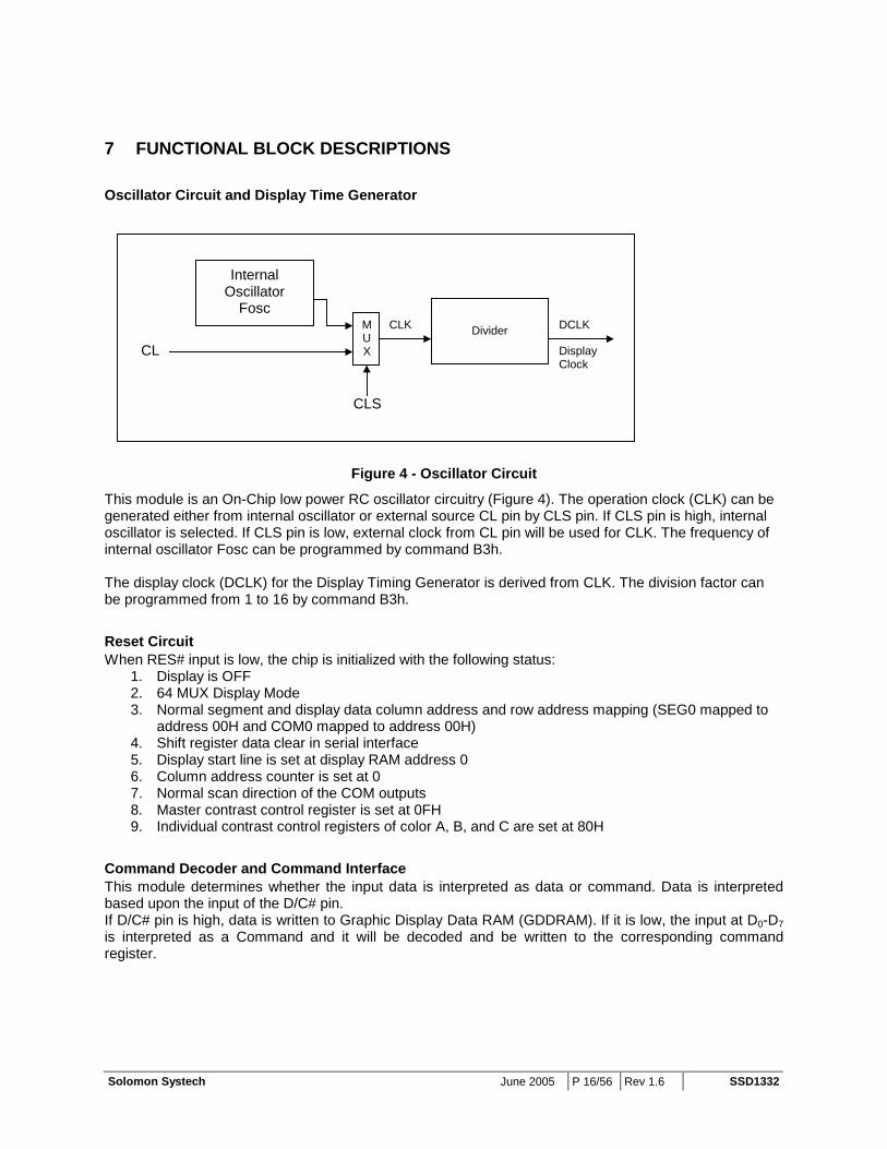
Oscillator Circuit and Display Time Generator
Divider
Internal Oscillator
Fosc MUXCL
CLK DCLK
Display Clock
CLS
Figure 4 - Oscillator Circuit
This module is an On-Chip low power RC oscillator circuitry (Figure 4). The operation clock (CLK) can be generated either from internal oscillator or external source CL pin by CLS pin. If CLS pin is high, internal oscillator is selected. If CLS pin is low, external clock from CL pin will be used for CLK. The frequency of internal oscillator Fosc can be programmed by command B3h. The display clock (DCLK) for the Display Timing Generator is derived from CLK. The division factor can be programmed from 1 to 16 by command B3h.
Reset Circuit When RES# input is low, the chip is initialized with the following status:
1. Display is OFF 2. 64 MUX Display Mode 3. Normal segment and display data column address and row address mapping (SEG0 mapped to
address 00H and COM0 mapped to address 00H) 4. Shift register data clear in serial interface 5. Display start line is set at display RAM address 0 6. Column address counter is set at 0 7. Normal scan direction of the COM outputs 8. Master contrast control register is set at 0FH 9. Individual contrast control registers of color A, B, and C are set at 80H
Command Decoder and Command Interface This module determines whether the input data is interpreted as data or command. Data is interpreted based upon the input of the D/C# pin. If D/C# pin is high, data is written to Graphic Display Data RAM (GDDRAM). If it is low, the input at D0-D7 is interpreted as a Command and it will be decoded and be written to the corresponding command register.

SSD1332 Rev 1.6 P 17/56 June 2005 Solomon Systech
Current and Voltage Supply This block is used to derive the incoming power sources into the different levels of internal use voltage and current.
• VCC are most positive voltage supply. It can be supplied externally or from internal DC-DC converter.
• VDD are external power supply for logic operation of the driver. • VREF is reference voltage, which is used to derive driving voltage for segments and commons like
VPA, VPB, VPC and VCOMH. Normally, VREF is connected to VCC. Please refer to the command table for the relationships of VREF to the segments and commons voltages.
• IREF is a reference current source for segment current drivers ISEG. The relationship between reference current and segment current of a color is:
ISEG = Contrast / 256 * IREF * scale factor in which the contrast (0~255) is set by Set Contrast command, and the scale factor (1 ~ 16) is set by Master Current Control command.
For example, in order to achieve ISEG = 160uA at maximum contrast 255, IREF is set to around 10uA. This current value is obtained by connecting an appropriate resistor from IREF pin to VSS as shown in Figure 5. Recommended range for Iref = 8 – 12uA
Figure 5 – IREF Current Setting by Resistor Value
Since the voltage at IREF pin is VCC – 3V, the value of resistor R1 can be found as below.
R1 = (Voltage at IREF – VSS) / IREF = (VCC – 3) / 10uA ≈ 910kΩ for VCC = 12V.
SSD1332
IREF (voltage at this pin = VCC – 3)
R1
VSS
IREF ≈ 10uA

Solomon Sys
Segment Drivers/Common Drivers Segment drivers consists of 288 (96 x 3 colors) current sources to drive OLED panel. The driving current can be adjusted from 0 to 200uA with 256 steps by contrast setting command. Common drivers generate scanning voltage pulse. The block diagrams and waveforms of the segment and common driver are shown as follow.
VCOMH
c
Current Drive
g
Non-select Row
te
Reset OLED Pixel
SelectedRow
ch June 2005 P 18/5
Figure 6 – Segment and Common Driver Block Diag
Vss
Common Driver
Segm
Vc
6 Rev 1
ram
Vss
ent D
Ise
.6 SSD1332
river

SSD1332 Rev 1.6 P 19/56 June 2005 Solomon Systech
Figure 7 – Segment and Common Driver Signal Waveform
Segment Voltage
e
Com Voltage
e
VCOMH
VCOMH
Com 0
Com 1
One Frame Period
N
Non-select Row
Selected Row
Tim
VSSVpa,Vpb,Vpc
Tim
VCOMH
VSS
This row is selected to turn on
VSS
VSS
Waveform for O
Waveform for OFF

S
The commons are scanned sequentially one by one row. If the row is not selected, all the pixels on the row are in reverse bias by driving those commons to voltage VCOMH. In the scanned row, the pixels on the row will be turned on or off by sending the corresponding data signal to the segment pins. If the pixel is turned off, the segment current is kept at 0. On the other hand, the segment drives to ISEG when the pixel is turned on. There are three phases to driving a OLED a pixel. In phase 1, the pixel is reset by the segment driver to VSS in order to discharge the previous data charge stored in the parasitic capacitance along the segment electrode. The period of phase 1 can be programmed by command B1h from 1 to 16 DCLK. An OLED panel with larger capacitance requires a longer period for discharging. In phase 2, the pixel is charged up by the segment driver to the desired voltage levels VPA, VPB or VPC for color A, B or C respectively. The period of phase 2 can be programmed by command B1h from 1 to 16 DCLK. An OLED panel with larger capacitance requires a longer period for charging up. Last phase is current drive stage. The current source in the segment driver delivers constant current to the pixel. The driver IC employs PWM (Pulse Width Modulation) method to control the gray scale of each pixel individually. The wider pulse widths in the current drive stage results in brighter pixels and vice versa. This is shown in the following figure.
ThTa
Segment Voltage
VSS
olomon Systech June 2005 P 20/56 Rev 1.6 SSD1332
Figure 8 – Gray Scale Control by PWM in Segment
e pulse width in current drive stage to control brightness can be programmed through “Set Gray Scale ble” command. It is described in more detailed in “Command Descriptions” section.
OLED Panel
Wider pulse width drives pixel brighter
e
Tim
SSD1332 Rev 1.6 P 21/56 June 2005 Solomon Systech
MPU Parallel 6800-series Interface The parallel interface consists of 8 bi-directional data pins (D0-D7), R/W(WR#), D/C, E (RD#) and CS#. R/W(WR#) High Input indicates a read operation from the Graphic Display Data RAM (GDDRAM) or the status register. R/W(WR#) Low Input indicates a write operation to Display Data RAM or Internal Command Registers depending on the status of D/C input. The E(RD#) input serves as data latch signal (clock) when high provided that CS# is low. Refer to Figure 27 of parallel timing characteristics for Parallel Interface Timing Diagram of 6800-series microprocessors. In order to match the operating frequency of display RAM with that of the microprocessor, some pipeline processing is internally performed which requires the insertion of a dummy read before the first actual display data read. This is shown in Figure 9 below.
n+2 n+1
Write column address Dummy read Data read1
R/ W(WR#)
Data bus N n
E(RD#)
Data read2 Data read3
Figure 9 - Display data read back procedure - insertion of dummy read
MPU Parallel 8080-series Interface The parallel interface consists of 8 bi-directional data pins (D0-D7), E (RD#), R/W(WR#), D/C and CS#. The E(RD#) input serves as data read latch signal (clock) when low, provided that CS# is low. Display data RAM or status register read is controlled by D/C#. R/W(WR#) input serves as data write latch signal (clock) when low provided that CS# is low, or CS# input serves as data write latch signal at rising edge when R/W(WR#) is low. Display data RAM or command register write is controlled by D/C. Refer to Figure 28 of parallel timing characteristics for Parallel Interface Timing Diagram of 8080-series microprocessor. Similar to 6800-series interface, a dummy read is also required before the first actual display data read.
MPU Serial Interface The serial interface consists of serial clock SCLK, serial data SDIN, D/C#, CS#. In SPI mode, D0 acts as SCLK, D1 acts as SDIN. For the unused data pins, D2 should be left open. D3 to D7, E and R/W pins can be connected to external ground. SDIN is shifted into an 8-bit shift register on every rising edge of SCLK in the order of D7, D6, ... D0. D/C# is sampled on every eighth clock and the data byte in the shift register is written to the Display Data RAM or command register in the same clock.

Solomon Systech June 2005 P 22/56 Rev 1.6 SSD1332
Graphic Display Data RAM (GDDRAM) The GDDRAM is a bit mapped static RAM holding the pattern to be displayed. The size of the RAM is 96 x 64 x 16bits. For mechanical flexibility, re-mapping on both Segment and Common outputs can be selected by software. For vertical scrolling of the display, an internal register storing display start line can be set to control the portion of the RAM data to be mapped to the display. Each pixel has 16-bit data. Three sub-pixels for color A, B and C have 6 bits, 5 bits and 6 bits respectively. The arrangement of data pixel in graphic display data RAM is shown below.
Figure 10 – 65k Color Depth Graphic Display Data RAM Structure
The sequence of sending one pixel of 16-bit data is divided into two 8-bit sessions as shown below.
Bit 7 Bit 6 Bit 5 Bit 4 Bit 3 Bit 2 Bit 1 Bit 0 1st byte C4 C3 C2 C1 C0 B5 B4 B3 2nd byte B2 B1 B0 A4 A3 A2 A1 A0
Figure 11 – 65k Color Depth Graphic Display Data Writing Sequence
In 256-color mode, each pixel is composed of 8-bit. Color A uses 2-bit while color B and color C each is represented by 3-bit. Although only 8 bits are required to represent one pixel, each pixel occupies 16-bit space inside graphic display data RAM with format as follows. For 256-color mode, one pixel data is sent in a 8-bit session like below.
Bit 7 Bit 6 Bit 5 Bit 4 Bit 3 Bit 2 Bit 1 Bit 0 1st byte C2 C1 C0 B2 B1 B0 A1 A0
Figure 11 – 256 Color Depth Graphic Display Data Writing Sequence
Normal :Remap :
A4 B5 C4 A4 B5 C4 A4 B5 C4 A4 B5 C4 A4 B5 C4 A4 B5 C4A3 B4 C3 A3 B4 C3 A3 B4 C3 A3 B4 C3 A3 B4 C3 A3 B4 C3A2 B3 C2 A2 B3 C2 A2 B3 C2 A2 B3 C2 A2 B3 C2 A2 B3 C2A1 B2 C1 A1 B2 C1 A1 B2 C1 A1 B2 C1 A1 B2 C1 A1 B2 C1A0 B1 C0 A0 B1 C0 A0 B1 C0 A0 B1 C0 A0 B1 C0 A0 B1 C0
B0 B0 B0 B0 B0 B0 COM
Normal Remap OUTPUT
0 95 5 6 5 5 6 5 5 6 5 5 6 5 5 6 5 5 6 5 COM01 94 COM12 93 COM2
: : :
93 2 COM6194 1 COM6295 0 COM63
SA0 SB0 SC0 SA1 SB1 SC1 SA2 SB2 SC2 : SA93 SB93 SC93 SA94 SB94 SC94 SA95 SB95 SC95
:
:
Data Format
Row
Address
293
932
0 95
:
Column Address
SEG OUTPUT
1 95 0 94 1
94
no. of bits of data in this cell

SSD1332 Rev 1.6 P 23/56 June 2005
Color C (3 bits)
RAM Content ( 5 bits)
000 00000 001 00100 010 01000 011 01100 100 10010 101 10110 110 11010 111 11110
Figure 12 – 256 Color Depth Graphi
Gray Scale and Gray Scale Table The gray scale display is produced by controllingcurrent drive phase. The gray scale table stores gray scale levels (GS0~GS63). The wider the puscale table supports all the three colors A, B and As shown in figure 13, color B sub-pixel RAM dGS0 to GS63. color A and color C sub-pixel RAMGS0, GS2, …, GS62.
Color A, C RAM data (5 bits)
ColorRAM data
0 0 - 1 1 2 - 3 2 4 : : : : : :
30 60- 61
31 62- 63
Figure 13 – Relation between graphic data RA65K
Color B (3 bits)
RAM Content ( 6 bits)
000 000000 001 001000 010 010000 011 011000 100 100100 101 101100 110 110100 111 111100
c Display Data RAM Structu
the current pulse widths frothe corresponding pulse widtlse width, the brighter the pi
C. The pulse widths are enter
ata has 6 bits, represent the data has only 5 bits, represe
B (6 bits)
Gray Sca
GS0 GS 1 GS 2 GS 3 GS 4
: : :
GS 60 GS 61 GS 62 GS 63
M value and gray scale tablcolor mode
Color A (2 bits)
RAM Content ( 5 bits)
00 00000 01 01000 10 10100 11 11100
Solomon Systech
re for One Pixel
m the segment driver in the hs (PW0 ~ PW63) of the 64 xel will be. This single gray ed by software commands.
64 gray scale levels from nt 32 gray scale levels from
le
e entry for three colors in

Solomon Systech June 2005 P 24/56 Rev 1.6 SSD1332
The meaning of values inside data RAM with respect to the gray scale level is best to be illustrated in an example below.
Gray Scale (Pulse Width)
Value/DCLKs
PW0 0 PW1 2 PW2 5
: : PW62 120 PW63 125
Figure 14 – illustration of relation between graphic display RAM value and gray scale control
Segment Voltage
e
Color B RAM data = 000001PW1
pulse width = 2 DCLKs
Color B RAM data = 111111 PW125
pulse width = 125 DCLKs
Gray Scale Table
Segment Voltage
Color A RAM data = 00001 PW2
pulse width = 5 DCLKs
Color A RAM data = 11111 PW62
pulse width = 120 DCLKs
Tim
VSSe
Tim VSS
SSD1332 Rev 1.6 P 25/56 June 2005 Solomon Systech
DC-DC Voltage Converter
VDDB
VBREF
VSSB
GDR
RESE
FB
+VDD
AGND
+
DGND
AGND
+
AGND
+
VCCL1 D1
Q1
R1
R2+
C4
C3C2
C1
C5
+
C6+
C7R3
Figure 15 – DC-DC Converter Application Circuit Diagram
It is a switching voltage generator circuit, designed for handheld applications. In SSD1332, internal DC-DC voltage converter accompanying with an external application circuit (shown in Figure 15) can generate a high voltage supply VCC from a low voltage supply input VDD. VCC is the voltage supply to the OLED driver block. The application circuit above is an example for the input voltage of 3V VDD to generate VCC of 12V @20mA ~ 30mA application. *ALL PATHS TO AGND SHOULD BE CONNECTED AS SHORT AS POSSIBLE Passive components selection:
Table 4 – Components Selection for DC-DC Converter
Components Typical Value Remark L1 Inductor, 22µH 2A D1 Schottky diode 2A, 25V e.g. 1N5822 Q1 MOSFET N-FET with low RDS(on) and low Vth voltage.
e.g. MGSF1N02LT1 [ON SEMICONDUCTOR] R1, R2 Resistor 1%,1/10W R3 Resistor, 1.2Ω 1%, 1/2W C1 Capacitor, 1µF 16V C2 Capacitor, 22µF Low ESR, 25V C3 Capacitor, 1µF 16V C4 Capacitor, 10nF 16V C5 Capacitor, 1 ~ 10 µF 16V C6 Capacitor, 0.1 ~ 1µF 16V C7 Capacitor, 15nF 16V
The VCC output voltage level can be adjusted by R1 and R2, the reference formula is: VCC = 1.2 x (R1+R2) / R2

Solomon Systech June 2005 P 26/56 Rev 1.6 SSD1332
8 COMMAND TABLE Table 5 – Configuration Command Table
(To write commands to command registers, the MCU interface pins are set as: D/C = 0, R/W(WR#) = 0, E (RD#)=1)
D/C Hex D7 D6 D5 D4 D3 D2 D1 D0 Command Description 0 15 0 0 0 1 0 1 0 1 A[6:0] sets the column start address from 0-95, POR=00d. 0 A[6:0] * A6 A5 A4 A3 A2 A1 A0 B[6:0] sets the column end address from 0-95 POR=95d. 0 B[6: 0] * B6 B5 B4 B3 B2 B1 B0
Set Column Address
0 75 0 1 1 1 0 1 0 1 A[5:0] sets the row start address from 0-63, POR=00d. 0 A[5:0] * * A5 A4 A3 A2 A1 A0 B[5:0] sets the row end address from 0-63, POR=63d. 0 B[5:0] * * B5 B4 B3 B2 B1 B0
Set Row Address
0 81 1 0 0 0 0 0 0 1 0 A[7:0] A7 A6 A5 A4 A3 A2 A1 A0 Set Contrast for Color
A (Segment Pins :SA0 –
SA95)
Double byte command to select 1 out of 256 contrast steps. Contrast increases as level increases. POR = 80H
0 82 1 0 0 0 0 0 1 0 0 A[7:0] A7 A6 A5 A4 A3 A2 A1 A0 Set Contrast for Color
B (Segment Pins :SB0 –
SB95)
Double byte command to select 1 out of 256 contrast steps. Contrast increases as level increases. POR = 80H
0 83 1 0 0 0 0 0 1 1 Set Contrast for Color C
0 A[7:0] A7 A6 A5 A4 A3 A2 A1 A0 (Segment Pins :SC0 – SC95)
Double byte command to select 1 out of 256 contrast steps. Contrast increases as level increases. POR = 80H
0 87 1 0 0 0 0 1 1 1
0 A[3:0] * * * * A3 A2 A1 A0
Master Current Control
Set A[3:0] from 0000, 0001… to 1111 to adjust the master current attenuation factor from 1/16, 2/16… to 16/16. POR =1111b, for no attenuation.

SSD1332 Rev 1.6 P 27/56 June 2005 Solomon Systech
0 A0 1 0 1 0 0 0 0 0 A[0]=0, Horizontal address increment (POR) 0 A[7:0] A7 A6 A5 A4 * * A1 A0 A[0]=1, Vertical address increment
A[1]=0, Column address 0 is mapped to SEG0 (POR) A[1]=1, Column address 95 is mapped to SEG0 A[4]=0, Scan from COM 0 to COM [N –1] A[4]=1, Scan from COM [N-1] to COM0. Where N is the
Multiplex ratio. A[5]=0, Disable COM Split Odd Even (POR) A[5]=1, Enable COM Split Odd Even A[7:6]=00; 256 color format = 01; 65k color format(POR)
Set Re-map & Data Format
Set display RAM display start line register from 0-63.
0 A1 1 0 1 0 0 0 0 1 Display start line register is reset to 00H after POR. 0 A[5:0] * * A5 A4 A3 A2 A1 A0
Set Display Start Line
0 A2 1 0 1 0 0 0 1 0 Set vertical scroll by COM from 0-63. 0 A[5:0] * * A5 A4 A3 A2 A1 A0 The value is reset to 00H after POR.
Set Display Offset
0 A4~A7 1 0 1 0 0 1 X1 X0 A4h=Normal Display (POR) A5h=Entire Display On, all pixels turn on at GS level 63 A6h=Entire Display Off, all pixels turn off A7h=Inverse Display
Set Display Mode
The next command determines multiplex
0 A8 1 0 1 0 1 0 0 0 ratio N from 16MUX-64MUX, POR=63d (64MUX)
0 A[5:0] * * A5 A4 A3 A2 A1 A0 A[5:0]=0-14d (invalid entry)
Set Multiplex Ratio
0 AD 1 0 1 0 1 1 0 1 Set Master A[0]=0, Select external VCC supply at Display ON 0 A[7:0] 1 0 0 0 1 A2 A1 A0 Configuration A[0]=1, Select internal booster at Display ON (POR) A[1]=0, Select external VCOMH voltage supply at Display ON A[1]=1, Select internal VCOMH regulator at Display ON (POR) A[2]=0, Select External VP voltage supply A[2]=1, Select Internal VP (POR)
0 AE~AF 1 0 1 0 X3 1 1 1 AEh=Display off (POR)
Set Display On/Off AFh=Display on
0 B0 1 0 1 1 0 0 0 0 Set Power Save A[7:0]=00 (POR) 0 A[7:0] 0 0 0 A4 0 0 A1 0 A[7:0]=12, power saving mode 0 B1 1 0 1 1 0 0 0 1 Phase 1 and 2 A[3:0] Phase 1 period in 1~16 DCLK clocks [POR=4h] 0 A[7:0] A7 A6 A5 A4 A3 A2 A1 A0 period adjustment A[7:4] Phase 2 period in 1~16 DCLK clocks [POR=7h]

Solomon Systech June 2005 P 28/56 Rev 1.6 SSD1332
0 B3 1 0 1 1 0 0 1 1 Display Clock Divider / A[3:0] [DIVIDER, POR=0] 0 A[7:0] A7 A6 A5 A4 A3 A2 A1 A0 Oscillator Frequency DCLK is generated from CLK divided by DIVIDER +1 (i.e., 1 to 16) A[7:4] Fosc frequency, POR=D0H Frequency increases as level increases
0 B8 1 0 1 1 1 0 0 0 The next 32 bytes of command set the current drive pulse width of gray scale level GS1, GS3, GS5 …GS63 as below:
0 A[7:0]--PW1
A7 A6 A5 A4 A3 A2 A1 A0 A[7:0]=PW1, POR=1, it equals 1 DCLK clock
0 B[7:0]--PW3
B7 B6 B5 B4 B3 B2 B1 B0 B[7:0]=PW3, POR=5, it equals 3 DCLK clocks
0 C[7:0]--PW5
C7 C6 C5 C4 C3 C2 C1 C0 C[7:0]=PW5, POR= 9
0 : : 0 : : 0 : : 0 AE[7:0]--
PW61 AE7 AE6 AE5 AE4 AE3 AE2 AE1 AE0
AE[7:0]=PW61, POR=121 0 AF[7:0]--
PW63 AF7 AF6 AF5 AF4 AF3 AF2 AF1 AF0
AF[7:0]=PW63, POR=125, it equals 125 DCLK clocks Note: GS0 has no pre-charge and current drive stages. For GS2 GS4…GS62, they are derived by driver itself with: PWn = (PWn-1+PWn+1)/2
Set Gray Scale Table
Max pulse width is 125
0 B9 1 0 1 1 1 0 0 1 Enable build-in linear gray scale table (POR=Enable) Enable Linear PW1=1,PW2=3,PW3=5 Gray Scale Table … PW61=121,PW62=123,PW63=125
0 BB ~ BD 1 0 1 1 1 X2 X1 X0 011b for Color A, 100b for Color B, 101b for Color C 0 A[7:0] A7 A6 A5 A4 A3 A2 A1 A0 A[7:0] 00000000 0.43*Vref 00111111 0.83*Vref 01111111 1.0*Vref
VPA, VPB, VPC level setting for Color A,B,C
1xxxxxxx connects to VCOMH (POR) 0 BE 1 0 1 1 1 1 1 0 A[6:0] 0000000 0.43*Vref 0 A[6:0] * A6 A5 A4 A3 A2 A1 A0 0111111 0.83*Vref (POR)
Set VCOMH
0 E3 1 1 1 0 0 0 1 1 NOP Command for No Operation

SSD1332 Rev 1.6 P 29/56 June 2005 Solomon Systech
Table 6 – Graphic Acceleration Command Set Table
(To write commands to command registers, the MCU interface pins are set as: D/C = 0, R/W(WR#)=0, E (RD#)=1)
D/C Hex D7 D6 D5 D4 D3 D2 D1 D0 Command Description 0 21 0 0 1 0 0 0 0 1 A[6:0] : Column Address of Start 0 A[6:0] * A6 A5 A4 A3 A2 A1 A0 B[5:0] : Row Address of Start 0 B[5:0] * * B5 B4 B3 B2 B1 B0 C[6:0] : Column Address of End 0 C[6:0] * C6 C5 C4 C3 C2 C1 C0 D[5:0] : Row Address of End 0 D[5:0] * * D5 D4 D3 D2 D1 D0 E[5:1] : Color C of the line 0 E[5:1] * * E5 E4 E3 E2 E1 * F[5:0] : Color B of the line 0 F[5:0] * * F5 F4 F3 F2 F1 F0 G[5:1] : Color A of the line 0 G[5:1] * * G5 G4 G3 G2 G1 *
Draw Line
0 22 0 0 1 0 0 0 1 0 A[6:0] : Column Address of Start 0 A[6:0] * A6 A5 A4 A3 A2 A1 A0 B[5:0] : Row Address of Start 0 B[5:0] * * B5 B4 B3 B2 B1 B0 C[6:0] : Column Address of End 0 C[6:0] * C6 C5 C4 C3 C2 C1 C0 D[5:0] : Row Address of End 0 D[5:0] * * D5 D4 D3 D2 D1 D0 E[5:1] : Color C of the line 0 E[5:1] * * E5 E4 E3 E2 E1 * F[5:0] : Color B of the line 0 F[5:0] * * F5 F4 F3 F2 F1 F0 G[5:1] : Color A of the line 0 G[5:1] * * G5 G4 G3 G2 G1 * H[5:1] : Color C of the fill area 0 H[5:1] * * H5 H4 H3 H2 H1 * I[5:0] : Color B of the fill area 0 I[5:0] * * I5 I4 I3 I2 I1 I0 J[5:1] : Color A of the fill area 0 J[5:1] * * J5 J4 J3 J2 J1 *
Drawing Rectangle
0 23 0 0 1 0 0 0 1 1 A[6:0] : Column Address of Start 0 A[6:0] * A6 A5 A4 A3 A2 A1 A0 B[5:0] : Row Address of Start 0 B[5:0] * * B5 B4 B3 B2 B1 B0 C[6:0] : Column Address of End 0 C[6:0] * C6 C5 C4 C3 C2 C1 C0 D[5:0] : Row Address of End 0 D[5:0] * * D5 D4 D3 D2 D1 D0 E[6:0] : Column Address of New Start 0 E[6:0] * E6 E5 E4 E3 E2 E1 E0 F[5:0] : Row Address of New Start 0 F[5:0] * * F5 F4 F3 F2 F1 F0
Copy
0 24 0 0 1 0 0 1 0 0 A[6:0] : Column Address of Start 0 A[6:0] * A6 A5 A4 A3 A2 A1 A0 B[5:0] : Row Address of Start 0 B[5:0] * * B5 B4 B3 B2 B1 B0 C[6:0] : Column Address of End 0 C[6:0] * C6 C5 C4 C3 C2 C1 C0 D[5:0] : Row Address of End 0 D[5:0] * * D5 D4 D3 D2 D1 D0 The effect of dim window: GS15~GS0 no change GS19~GS16 become GS4 GS23~GS20 become GS5 ...
Dim Window
GS63~GS60 become GS15 0 25 0 0 1 0 0 1 0 1 A[6:0] : Column Address of Start 0 A[6:0] * A6 A5 A4 A3 A2 A1 A0 B[5:0] : Row Address of Start 0 B[5:0] * * B5 B4 B3 B2 B1 B0 C[6:0] : Column Address of End 0 C[6:0] * C6 C5 C4 C3 C2 C1 C0 D[5:0] : Row Address of End 0 D[5:0] * * D5 D4 D3 D2 D1 D0
Clear Window

Solomon Systech June 2005 P 30/56 Rev 1.6 SSD1332
D/C Hex D7 D6 D5 D4 D3 D2 D1 D0 Command Description 0 26 0 0 1 0 0 1 1 0 A0 0 : Disable Fill for Draw Rectangle Command (POR) 0 A[4:0] * * * A4 0 0 0 A0 1 : Enable Fill for Draw Rectangle Command A[3:1] 000 : Reserved values A4 0 : Disable reverse copy (POR) 1 : Enable reverse during copy command.
Fill Enable / Disable
Table 7 - Read Command Table
(D/C=0, R/W (WR#)=1, E (RD#)=1 for 6800 or E (RD#)=0 for 8080) Bit Pattern Command Description
D7D6D5D4D3D2D1D0
Status Register Read *
D7 : “1” for Command lock D6 : “1” for display OFF / “0” for display ON D5 : Reserve D4 : Reserve D3 : Reserve D2 : Reserve D1 : Reserve D0 : Reserve
Note: Patterns other than that given in Command Table are prohibited to enter to the chip as a command; otherwise, unexpected result will occur.
Data Read / Write To read data from the GDDRAM, input HIGH to R/W (WR#) pin and D/C pin for 6800-series parallel mode, LOW to E (RD#) pin and HIGH to D/C pin for 8080-series parallel mode. No data read is provided in serial mode operation. In normal data read mode, GDDRAM column address pointer will be increased by one automatically after each data read. Also, a dummy read is required before the first data read. See Figure 5 in Functional Block Description. To write data to the GDDRAM, input LOW to R/W (WR#) pin and HIGH to D/C pin for 6800-series parallel mode AND 8080-series parallel mode. For serial interface mode, it is always in write mode. GDDRAM column address pointer will be increased by one automatically after each data write.
Table 8 - Address increment table (Automatic)
D/C
R/W (WR#)
Comment
Address Increment
0 0 Write Command No 0 1 Read Status No 1 0 Write Data Yes 1 1 Read Data Yes

SSD1332 Rev 1.6 P 31/56 June 2005 Solomon Systech
9 COMMAND DESCRIPTIONS Set Column Address (15h) This command specifies column start address and end address of the display data RAM. This command also sets the column address pointer to column start address. This pointer is used to define the current read/write column address in graphic display data RAM. If horizontal address increment mode is enabled by command A0h, after finishing read/write one column data, it is incremented automatically to the next column address. Whenever the column address pointer finishes accessing the end column address, it is reset back to start column address. Set Row Address (75h) This command specifies row start address and end address of the display data RAM. This command also sets the row address pointer to row start address. This pointer is used to define the current read/write row address in graphic display data RAM. If vertical address increment mode is enabled by command A0h, after finishing read/write one row data, it is incremented automatically to the next row address. Whenever the row address pointer finishes accessing the end row address, it is reset back to start row address. For example, column start address is set to 2 and column end address is set to 93, row start address is set to 1 and row end address is set to 62. Horizontal address increment mode is enabled by command A0h. In this case, the graphic display data RAM column accessible range is from column 2 to column 93 and from row 1 to row 62 only. In addition, the column address pointer is set to 2 and row address pointer is set to 1. After finishing read/write one pixel of data, the column address is increased automatically by 1 to access the next RAM location for next read/write operation. Whenever the column address pointer finishes accessing the end column 93, it is reset back to column 2 and row address is automatically increased by 1. While the end row 62 and end column 93 RAM location is accessed, the row address is reset back to 1. The diagram below shows the way of column and row address pointer movement for this example.
Col 0 Col 1 Col 2 ….. ……. Col 93 Col 94 Col 95
Row 0
Row 1
Row 2
: :
: :
: :
Row 61
Row 62
Row 63
Figure 16 – Example of Column and Row Address Pointer Movement

Solomon Systech June 2005 P 32/56 Rev 1.6 SSD1332
Set Contrast for Color A, B, C (81h, 82h, 83h) This command is to set Contrast Setting of each color A, B and C. The chip has three contrast control circuits for color A, B and C. Each contrast circuit has 256 contrast steps from 00h to FFh. The segment output current ISEG increases linearly with the contrast step, which results in brighter of the color. This relation is shown in Figure 17. In many situations, the output brightness of color A, B and C pixels are different under the same segment current condition. The contrasts of color A, B and C are set such that the brightness of each color are the same on the OLED panel Master Current Control (87h) This command is to control the segment output current by a scale factor. This factor is common to color A, B and C. The chip has 16 master control steps. The factor is ranged from 1 [0000] to 16 [1111]. POR is 16 [1111]. The smaller the master current value, the dimmer the OLED panel display is set. For example, if original segment output current of a color is 160uA at scale factor = 16, setting scale factor to 8 to reduce the current to 80uA. Please see Figure 17.
Segment output current
0
50
100
150
200
00 0F 1F 2F 3F 4F 5F 6F 7F 8F 9F AF BF CF DF EF FF
Cont r as t set t i ng
Out
put
curr
ent
Iseg
(uA
)
Master current setting
0F0E0D0C0B0A09080706050403020100
Figure 17 – Segment Output Current for Different Contrast Control and Master Current Setting
Change contrast control moves along the contrast curve with constant slope
Change master current selects different contrast slope.

SSD1332 Rev 1.6 P 33/56 June 2005 Solomon Systech
Set Re-map & Data Format (A0h) This command has multiple configurations and each bit setting is described as follows.
• Address increment mode (A[0]) When it is set to 0, the driver is set as horizontal address increment mode. After the display RAM is read/written, the column address pointer is increased automatically by 1. If the column address pointer reaches column end address, the column address pointer is reset to column start address and row address pointer is increased by 1. The sequence of movement of the row and column address point for horizontal address increment mode is shown in Figure 18.
Col 0 Col 1 ….. Col 94 Col 95 Row 0 Row 1
: : : : : : Row 62 Row 63
Figure 18 – Address Pointer Movement of Horizontal Address Increment Mode
When A[0] is set to 1, the driver is set to vertical address increment mode. After the display RAM is read/written, the row address pointer is increased automatically by 1. if the row address pointer reaches the row end address, the row address pointer is reset to row start address and column address pointer is increased by 1. The sequence of movement of the row and column address point for vertical address increment mode is shown in Figure 19.
Col 0 Col 1 ….. Col 94 Col 95 Row 0 ….. Row 1 …..
: : Row 62 ….. Row 63 …..
Figure 19 – Address Pointer Movement of Vertical Address Increment Mode
• Column Address Mapping (A[1])
This command bit is made for flexible layout of segment signals in OLED module with segment arranged from left to right or vice versa.
• COM Remap (A[4]) This bit determines the scanning direction of the common for flexible layout of common signals in OLED module either from up to down or vice versa.
• Odd even split of COM pins (A[5]) This bit can set the odd even arrangement of COM pins. A[5] = 0: Disable COM split odd even, pin assignment of common is in sequential as
COM63 COM62 .... COM 33 COM32..SC95..SA0..COM0 COM1.... COM30 COM31 A[5] = 1: Enable COM split odd even, pin assignment of common is in odd even split as
COM63 COM61.... COM3 COM1..SC95..SA0..COM0 COM2.... COM60 COM62
• Display color mode (A[7:6]) Select either 65k or 256 color mode. The display RAM data format in different mode is described in section “Graphic Display Data RAM (GDDRAM)”.

Solomon Systech June 2005 P 34/56 Rev 1.6 SSD1332
Set Display Start Line (A1h) This command is to set Display Start Line register to determine starting address of display RAM to be displayed by selecting a value from 0 to 63. The figure below shows an example of this command. In there, “Row” means the graphic display data RAM row. 64 64 62 62 Mux ratio COM Pin 0 4 0 4 Display start
line COM0 Row0 Row4 Row0 Row4 COM1 Row1 Row5 Row1 Row5 COM2 Row2 Row6 Row2 Row6 COM3 Row3 Row7 Row3 Row7 : : : : : : : : : : COM57 Row57 Row61 Row57 Row61 COM58 Row58 Row62 Row58 Row62 COM59 Row59 Row63 Row59 Row63 COM60 Row60 Row0 Row60 Row0 COM61 Row61 Row1 Row61 Row1 COM62 Row62 Row2 - - COM63 Row63 Row3 - -
Figure 20 – Example of Set Display Start Line with no Remap
Set Display Offset (A2h) This command specifies the mapping of display start line (it is assumed that COM0 is the display start line, display start line register equals to 0) to one of COM0-63. For example, to move the COM16 towards the COM0 direction for 16 lines, the 6-bit data in the second command should be given by 0010000. The figure below shows an example of this command. In there, “Row” means the graphic display data RAM row. 64 64 62 62 Mux ratio COM Pin 0 4 0 4 Display offset COM0 Row0 Row4 Row0 Row4 COM1 Row1 Row5 Row1 Row5 COM2 Row2 Row6 Row2 Row6 COM3 Row3 Row7 Row3 Row7 : : : : : : : : : : COM57 Row57 Row61 Row57 Row61 COM58 Row58 Row62 Row58 - COM59 Row59 Row63 Row59 - COM60 Row60 Row0 Row60 Row0 COM61 Row61 Row1 Row61 Row1 COM62 Row62 Row2 - Row2 COM63 Row63 Row3 - Row3
Figure 21 – Example of Set Display Offset with no Remap

SSD1332 Rev 1.6 P 35/56 June 2005 Solomon Systech
Set Display Mode (A4h ~ A7h) These are single byte command and they are used to set Normal Display, Entire Display On, Entire Display Off and Inverse Display.
• Set Entire Display On (A5h) Forces the entire display to be at “GS63” regardless of the contents of the display data RAM.
• Set Entire Display Off (A6h) Forces the entire display to be at gray level “GS0” regardless of the contents of the display data RAM.
• Inverse Display (A7h) The gray level of display data are swapped such that “GS0” <-> “GS63”, “GS1” <-> “GS62”, ….
• Normal Display (A4h) Reset the above effect and turn the data to ON at the corresponding gray level.
Set Multiplex Ratio (A8h) This command switches default 1:64 multiplex mode to any multiplex mode from 16 to 64. For example, when multiplex ratio is set to 16, only 16 common pins are enabled. The starting and the ending of the enabled common pins are depended on the setting of “Display Offset” register programmed by command A2h. Set Master Configuration (ADh) This command contains multiple bits to control several functionalities of the driver.
• Select DC-DC converter (A[0]) 0 = Disable selection of DC-DC converter and VCC is supplied externally. 1 (POR) = Enable selection of DC-DC converter to supply high voltage to VCC. The output voltage of the converter is set by values of external resistors. Please refer to section “DC-DC Voltage Converter” for details.
• Select VCOMH supply (A[1]) 0 = Select external VCOMH voltage from VCOMH pin for the common waveform high voltage level supply. It is recommended to set the voltage of VCOMH such that the OLED pixel diode is not turned on (prefer in reverse bias state) when the segment pin is either driven to VPA, VPB or VPC level. 1 = Select internal VCOMH voltage generated by regulator from VREF. The level of VCOMH can be programmed by command BEh.
• Select pre-charge voltage supply (A[2]) 0 = Select pre-charge voltage sources from external pins VPA, VPB, VPC for color A, B and C respectively. 1 = Select pre-charge voltage supply internally. The level of VPA, VPB, VPC can be set by command BBh, BCh and BDh for color A, B and C respectively.
Set Display On/Off (AEh/AFh) These single byte commands are used to turn the OLED panel display on or off. When the display is on, the selected circuits by Set Master Configuration command will be turned on. When the display is off, those circuits will be turned off and the segment and common output are in high impedance state. Phase 1 and 2 Period Adjustment (B1h) This command sets the length of phase 1 and 2 of segment waveform of the driver.
• Phase 1 (A[3:0]): Set the period from 1 to 16 in the unit of DCLKs. A larger capacitance of the OLED pixel may require longer period to discharge the previous data charge completely.
• Phase 2 (A[7:4]): Set the period from 1 to 16 in the unit of DCLKs. A longer period is needed to charge up a larger capacitance of the OLED pixel to the target voltage VPA, VPB, VPC for color A, B and C respectively.

Solomon Systech June 2005 P 36/56 Rev 1.6 SSD1332
Set Display Clock Divide Ratio/ Oscillator Frequency (B3h) This command consists of two functions:
• Display Clock Divide Ratio (A[3:0]) Set the divide ratio to generate DCLK (Display Clock) from CLK. The divide ratio is from 1 to 16, with power on reset value = 1. Please refer to section “Oscillator Circuit and Display Time Generator” for the details of DCLK and CLK.
• Oscillator Frequency (A[7:4]) Program the oscillator frequency Fosc which is the source of CLK if CLS pin is pulled high. The 4-bit value results in 16 different frequency setting available as shown below. The default value is 1101b which represents 0.97MHz Fosc.
Set Gray Scale Table (B8h) This command is used to set the gray scale table for the display. Except gray scale entry 0, which is zero as it has no pre-charge and current drive, each odd entry gray scale level is programmed in the length of current drive stage pulse width with unit of DCLK. The longer the length of the pulse width, the brighter is the OLED pixel when it’s turned on. Please refer to section “Graphic Display Data RAM (GDDRAM)” for more detailed explanation of relation of display data RAM, gray scale table and the pixel brightness. Following the command B8h, the user has to set the pulse width from PW1, PW3, PW5, …, PW59, PW61, PW63 one by one in sequence and complies the following conditions.
PW1 > 0; PW3 > PW1 + 1; PW5 > PW3 + 1; …… Afterwards, the driver automatically derives the pulse width of even entry of gray scale table PW2, PW4, …, PW62 with the formula like below.
PWn = (PWn-1 + PWn+1) / 2
For example, if PW1 = 3 DCLKs and PW3 = 7 DCLKs, PW2 = (3+7)/2 = 5 DCLKs The setting of gray scale table entry can perform gamma correction on OLED panel display. Normally, it is desired that the brightness response of the panel is linearly proportional to the image data value in display data RAM. However, the OLED panel is somehow responded in non-linear way. Appropriate gray scale table setting like example below can compensate this effect.
Figure 22 – Example of gamma correction by gray scale table setting
Pulse Width
Gray Scale
Panel response
Brightness Brightness
Pulse width Gray Scale
Gray scale table setting
Result in linear response

SSD1332 Rev 1.6 P 37/56 June 2005 Solomon Systech
Enable Linear Gray Scale Table (B9h) This command reloads the preset linear gray scale table as PW1 = 1, PW2 = 3, PW3 = 5, …., PW62 = 123, PW63 = 125 DCLKs. Set VPA, VPB and VPC Voltage for Color A, B and C (BBh, BCh and BDh) These three commands are used to set VPA, VPB and VPC phase 2 voltage level for color A, B and C respectively. The commands are valid in condition that these voltages are selected to generate internally by command ADh. It can be programmed to set the pre-charge voltage reference to VREF or VCOMH. Set VCOMH Voltage (BEh) This command sets the high voltage level of common pins, VCOMH, when it is selected to generate internally by command ADh. The level of VCOMH is programmed with reference to VREF.

Solomon
10 GRAPHIC ACCELERATION COMMAND SET DESCRIPTION Draw Line (21h) This command draws a line by the given start, end column and row coordinates and the color of the line.
For exam
1. 2. 3. 4. 5. 6.
Draw RGiven thand fill adisabled
The follo
1. 2. 3. 4. 5. 6. 7.
1
2
OC
Row 1, Column
Systech
Figure 23 – Example of D
ple, the line above can be drawn by the followiEnter into draw line mode by command 21h Send column start address of line, column1, forSend row start address of line, row 1, for exampSend column end address of line, column 2, forSend row end address of line, row 2, for exampSend color C, B and A of line, for example = 35d
ectangle (22h) e starting point (Row 1, Column 1) and the enrea colors, a rectangle that will be drawn with, the enclosed area will not be filled.
Figure 24 – Example of Draw
wing example illustrates the rectangle drawing Enter the “draw rectangle mode” by execute theSet the starting column coordinates, Column 1. Set the starting row coordinates, Row 1. e.g., 02Set the finishing column coordinates, Column 2Set the finishing row coordinates, Row 2. e.g., 1Set the outline color C, B and A. e.g., (28d, 0d, Set the filled color C, B and A. e.g., (0d, 0d, 40d
1
Row Colum
utline olor
FC
Row 2, Column
LineColor
raw Line Command
ng command sequence.
example = 1h le = 10h
example = 28h le = 4h , 0d, 0d for blue color
ding point (Row 2, Column 2), specify the outline the color specified. Remarks: If fill color option is
Row 1, Column
June 2005 P 38/56 Rev 1.6 SSD1332
Rectangle Command
command sequence. command 22h e.g., 03h. h.
. e.g., 12h 5h 0d) for blue color ) for red color
2, n 2
illed olor

SSD1332 Rev 1.6 P 39/56 June 2005 Solomon Systech
Copy (23h) Copy the rectangular region defined by the starting point (Row 1, Column 1) and the ending point (Row 2, Column 2) to location (Row 3, Column 3). If the new coordinates are smaller than the ending points, the new image will overlap the original one. The following example illustrates the copy procedure.
1. Enter the “copy mode” by execute the command 23h 2. Set the starting column coordinates, Column 1. E.g., 00h. 3. Set the starting row coordinates, Row 1. E.g., 00h. 4. Set the finishing column coordinates, Column 2. E.g., 05h 5. Set the finishing row coordinates, Row 2. E.g., 05h 6. Set the new column coordinates, Column 3. E.g., 03h 7. Set the new row coordinates, Row 3. E.g., 03h
Figure 25 – Example of Copy Command
Dim Window (24h) This command will dim the window area specify by starting point (Row 1, Column 1) and the ending point (Row 2, Column 2). After the execution of this command, the selected window area will become darker as follow.
Table 9 – Result of Change of Brightness by Dim Window Command
Original gray scale New gray scale after dim window command GS0 ~ GS15 No change GS16 ~ GS19 GS4 GS20 ~ GS23 GS5
: : GS60 ~ GS63 GS15
Additional execution of this command over the same window area will not change the data content.
Row 3 + Row 2, Column 3 + Column 2
Row 1, Column 1
Row 3, Column 3
Original Image
New Copied Image

Solomon Systech June 2005 P 40/56 Rev 1.6 SSD1332
Clear Window (25h) This command sets the window area specify by starting point (Row 1, Column 1) and the ending point (Row 2, Column 2) to clear the window display. The graphic display data RAM content of the specified window area will be set to zero. This command can be combined with Copy command to make as a “move” result. The following example illustrates the copy plus clear procedure and results in moving the window object.
1. Enter the “copy mode” by execute the command 23h 2. Set the starting column coordinates, Column 1. E.g., 00h. 3. Set the starting row coordinates, Row 1. E.g., 00h. 4. Set the finishing column coordinates, Column 2. E.g., 05h 5. Set the finishing row coordinates, Row 2. E.g., 05h 6. Set the new column coordinates, Column 3. E.g., 06h 7. Set the new row coordinates, Row 3. E.g., 06h 8. Enter the “clear mode” by execute the command 24h 9. Set the starting column coordinates, Column 1. E.g., 00h. 10. Set the starting row coordinates, Row 1. E.g., 00h. 11. Set the finishing column coordinates, Column 2. E.g., 05h 12. Set the finishing row coordinates, Row 2. E.g., 05h
Figure 26 – Example of Copy + Clear = Move Command
Fill Enable/Disable (26h) This command has two functions.
• Enable/Disable fill (A[0]) 0 = Disable filling of color into rectangle in draw rectangle command. (POR) 1 = Enable filling of color into rectangle in draw rectangle command.
• Enable/Disable reverse copy (A[4]) 0 = Disable reverse copy (POR) 1 = During copy command, the new image colors are swapped such that “GS0” <-> “GS63”, “GS1” <-> “GS62”, ….
Row 3 + Row 2, Column 3 + Column 2
Row 1, Column 1
Row 3, Column 3
Original Image
New Copied Image
Clear Command

SSD1332 Rev 1.6 P 41/56 June 2005 Solomon Systech
11 MAXIMUM RATINGS Table 10 - Maximum Ratings
(Voltage Reference to VSS) Symbol Parameter Value Unit
VDD -0.3 to +4 V VCC 0 to 18 V VREF
Supply Voltage 0 to 18 V
VCOMH Supply Voltage/Output voltage 0 to 16 V - SEG/COM output voltage 0 to 16 V
Vin Input voltage Vss-0.3 to Vdd+0.3 V TA Operating Temperature -40 to +85 ºC Tstg Storage Temperature Range -65 to +150 ºC
*Maximum Ratings are those values beyond which damage to the device may occur. Functional operation should be restricted to the limits in the Electrical Characteristics tables or Pin Description.
12 DC CHARACTERISTICS Table 11 - DC Characteristics
(Unless otherwise specified, Voltage Referenced to VSS, VDD = 2.4 to 3.5V, TA = 25°C) Symbol Parameter Test Condition Min Typ Max Unit
Vcc Operating Voltage 7 11 18 V VDD Logic Supply Voltage 2.4 2.7 3.5 V
VOH High Logic Output Level Iout =100uA, 3.3MHz 0.9*VDD - VDD V
VOL Low Logic Output Level Iout =100uA, 3.3MHz 0 - 0.1*VDD V
VIH High Logic Input Level Iout =100uA, 3.3MHz 0.8*VDD - VDD V
VIL Low Logic Input Level Iout =100uA, 3.3MHz 0 - 0.2*VDD V
ISLEEP Sleep mode Current VDD=2.7V, Display OFF, No panel attached - -
5
uA
ICC Vcc Supply Current VDD=2.7V, VCC=11V, Display ON Contrast =FF, No panel attached - 770 - uA
IDD VDD Supply Current VDD=2.7V, VCC=11V, Display ON Contrast =FF, No panel attached - 170 - uA
Contrast = FF - 160 - uA Contrast = AF 110 uA Contrast = 5F - 60 - uA ISEG
Segment Output Current Setting VDD=2.7V, VCC=11V, IREF=10uA, All one pattern, Display on, Segment pin under test is connected with a 33KΩ resistive load to Vcc.
Contrast = 00 - 0 - uA
Dev Segment output current uniformity
Dev = (ISEG – IMID)/IMID
IMID = (IMAX + IMIN)/2
ISEG[0:287] = Segment current at
contrast = FF
- - 3 %
Adj. Dev Adjacent pin output current uniformity (contrast = FF) Adj Dev = (I[n]-I[n+1]) / (I[n]+I[n+1]) - ±2.0 -- %
Vcc Booster output voltage (Vcc) Vin=3V, L=22uH; R1=450Kohm;
R2=50Kohm; Icc = 30mA(soaking)
11 -
13
V
Pwr Booster output power Vin=3V, L=22uH; Vcc = 10 V ~ 16V - - 400 mW

Solomon Systech June 2005 P 42/56 Rev 1.6 SSD1332
13 AC CHARACTERISTICS Table 12 - AC Characteristics
(Unless otherwise specified, Voltage Referenced to VSS, VDD = 2.4 to 3.5V, TA = 25°C.) Symbol Parameter Test Condition Min Typ Max Unit FOSC Oscillation Frequency of Display
Timing Generator VDD = 2.7V - 0.97 - MHz
FFRM Frame Frequency for 64 MUX Mode
96RGB x 64 Graphic Display Mode, Display ON, Internal Oscillator Enabled
- FOSC X 1/(D*K*64) - Hz
D: divide ratio (POR=1) K: number of display clocks (POR=136, i.e. phase1 dclk+phase2 dclk+ phase3 dclk=4+7+125)

SSD1332 Rev 1.6 P 43/56 June 2005 Solomon Systech
Table 13 - 6800-Series MPU Parallel Interface Timing Characteristics
(VDD - VSS = 2.4 to 3.5V, TA = -40 to 85°C)
Symbol Parameter Min Typ Max Unit tcycle Clock Cycle Time 300 - - ns tAS Address Setup Time 0 - - ns tAH Address Hold Time 0 - - ns
tDSW Write Data Setup Time 40 - - ns tDHW Write Data Hold Time 15 - - ns tDHR Read Data Hold Time 20 - - ns tOH Output Disable Time - - 70 ns tACC Access Time - - 140 ns
PWCSL Chip Select Low Pulse Width (read) Chip Select Low Pulse Width (write)
120 60 - - ns
PWCSH Chip Select High Pulse Width (read) Chip Select High Pulse Width (write)
60 60 - - ns
tR Rise Time - - 15 ns tF Fall Time - - 15 ns
D0~D7(WRITE)
D0~D7(READ)
E
CS#
R/W#
PWCSL tR
tF tDHW
tOH
tACC tDHR
Valid Data
tDSW
Valid Data
tcyclePWCSH
tAH tAS
D/C#
Figure 27 - 6800-series MPU parallel interface characteristics

Solomon Systech June 2005 P 44/56 Rev 1.6 SSD1332
Table 14 - 8080-Series MPU Parallel Interface Timing Characteristics
(VDD - VSS = 2.4 to 3.5V, TA = -40 to 85°C) Symbol Parameter Min Typ Max Unit tcycle Clock Cycle Time 300 - - ns tAS Address Setup Time 0 - - ns tAH Address Hold Time 0 - - ns tDSW Write Data Setup Time 40 - - ns tDHW Write Data Hold Time 15 - - ns tDHR Read Data Hold Time 20 - - ns tOH Output Disable Time - - 70 ns tACC Access Time - - 140 ns PWCSL Chip Select Low Pulse Width (read)
Chip Select Low Pulse Width (write) 120 60
- - ns
PWCSH Chip Select High Pulse Width (read) Chip Select High Pulse Width (write)
60 60
- - ns
tR Rise Time - - 15 ns tF Fall Time - - 15 ns
Figure 28 - 8080-series MPU parallel interface characteristics
t
tDHRtACC
Valid Data
Valid Data
tDSW
tDHW
tRtF
PW CSL PW CSH tcycle
tAHtAS
D0-D15 (Read data from driver)
D0-D15 (Write data to driver)
WR#
RD#
CS#
D/C

SSD1332 Rev 1.6 P 45/56 June 2005 Solomon Systech
Table 15 - Serial Interface Timing Characteristics
(VDD - VSS = 2.4 to 3.5V, TA = -40 to 85°C) Symbol Parameter Min Typ Max Unit
tcycle Clock Cycle Time 250 - - ns
tAS Address Setup Time 150 - - ns tAH Address Hold Time 150 - - ns tCSS Chip Select Setup Time 120 - - ns tCSH Chip Select Hold Time 60 - - ns tDSW Write Data Setup Time 100 - - ns tDHW Write Data Hold Time 100 - - ns tCLKL Clock Low Time 100 - - ns tCLKH Clock High Time 100 - - ns tR Rise Time - - 15 ns tF Fall Time - - 15 ns
tAH tAS
D/C#
Valid Data
tDHW
tCLK
tDSW
tCLKHtcycle
tCSS tCSH
tF tR
SDIN(D1)
CS#
SCLK(D0)
D7 SDIN(D1)
CS#
SCLK(D0)
D6 D5 D4 D3 D2 D1 D0
Figure 29 - Serial interface characteristics
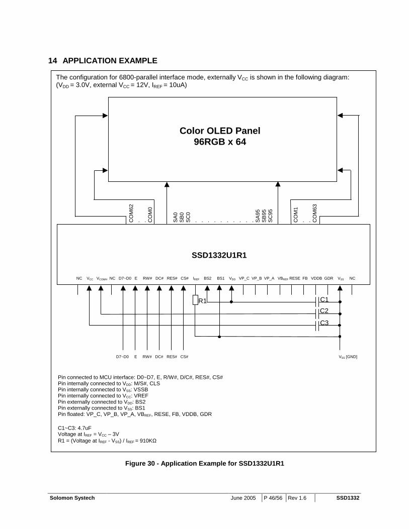
Solomon Systech
14 APPLICATION EXAMPLE
Figure 3
Color OLED Panel 96RGB x 64
CO
M62
. .
3
NC VCC VCOMH NC D7~D0 E RW
D7~D0 E RW
The configuration for 6800-parallel interface mode, externally VCC is shown in the following diagram: (VDD = 3.0V, external VCC = 12V, IREF = 10uA)
SSD1332U1R1
CO
M0
SA
0 S
B0
SC
0 . . . . . . . . . . S
A95
SB
95S
C95
CO
M1
. . CO
M6
# DC# RES# CS# IREF BS2 BS1 VDD VP_C VP_B VP_A VBREF RESE FB VDDB GDR VSS NC
# DC# RES# CS# VSS [GND]
1
3
2
Pin connected to MCU interface: D0~D7, E, R/W#, D/C#, RES#, CS#Pin internally connected to VDD: M/S#, CLS Pin internally connected to VSS: VSSB Pin internally connected to VCC: VREF Pin externally connected to VDD: BS2 Pin externally connected to VSS: BS1 Pin floated: VP_C, VP_B, VP_A, VBREF, RESE, FB, VDDB, GDR C1~C3: 4.7uF Voltage at IREF = VCC – 3V R1 = (Voltage at IREF - VSS) / IREF = 910KΩ
0 - Application
R1
June 2005 P 46/56 Rev 1.6
Example for SSD1332U1R1
C
C
C
SSD1332

SSD1332 Rev 1.6 P 47/56 June 2005 Solomon Systech
15 SSD1332U1R1 COF PACKAGE DIMENSIONS

Solomon Systech June 2005 P 48/56 Rev 1.6 SSD1332

SSD1332 Rev 1.6 P 49/56 June 2005 Solomon Systech
16 SSD1332U1R1 COF PIN ASSIGNMENT
Figure 31 - SSD1332U1R1 COF pin assignment

Solomon Systech June 2005 P 50/56 Rev 1.6 SSD1332
Pin # Pin name Pin # Pin name Pin # Pin name Pin # Pin name Pin # Pin name
1 NC 81 SA93 161 SB66 241 SC39 321 SA13 2 VCC 82 SC92 162 SA66 242 SB39 322 SC12 3 VCOMH 83 SB92 163 SC65 243 SA39 323 SB12 4 NC 84 SA92 164 SB65 244 SC38 324 SA12 5 D7 85 SC91 165 SA65 245 SB38 325 SC11 6 D6 86 SB91 166 SC64 246 SA38 326 SB11 7 D5 87 SA91 167 SB64 247 SC37 327 SA11 8 D4 88 SC90 168 SA64 248 SB37 328 SC10 9 D3 89 SB90 169 SC63 249 SA37 329 SB10
10 D2 90 SA90 170 SB63 250 SC36 330 SA10 11 D1 91 SC89 171 SA63 251 SB36 331 SC9 12 D0 92 SB89 172 SC62 252 SA36 332 SB9 13 E(RD#) 93 SA89 173 SB62 253 SC35 333 SA9 14 R/W#(WR#) 94 SC88 174 SA62 254 SB35 334 SC8 15 D/C# 95 SB88 175 SC61 255 SA35 335 SB8 16 RES 96 SA88 176 SB61 256 SC34 336 SA8 17 CS# 97 SC87 177 SA61 257 SB34 337 SC7 18 IREF 98 SB87 178 SC60 258 SA34 338 SB7 19 BS2 99 SA87 179 SB60 259 SC33 339 SA7 20 BS1 100 SC86 180 SA60 260 SB33 340 SC6 21 VDD 101 SB86 181 SC59 261 SA33 341 SB6 22 VP_C 102 SA86 182 SB59 262 SC32 342 SA6 23 VP_B 103 SC85 183 SA59 263 SB32 343 SC5 24 VP_A 104 SB85 184 SC58 264 SA32 344 SB5 25 VBREF 105 SA85 185 SB58 265 SC31 345 SA5 26 RESE 106 SC84 186 SA58 266 SB31 346 SC4 27 FB 107 SB84 187 SC57 267 SA31 347 SB4 28 VDDB 108 SA84 188 SB57 268 SC30 348 SA4 29 GDR 109 SC83 189 SA57 269 SB30 349 SC3 30 VSS 110 SB83 190 SC56 270 SA30 350 SB3 31 NC 111 SA83 191 SB56 271 SC29 351 SA3 32 NC 112 SC82 192 SA56 272 SB29 352 SC2 33 NC 113 SB82 193 SC55 273 SA29 353 SB2 34 NC 114 SA82 194 SB55 274 SC28 354 SA2 35 COM63 115 SC81 195 SA55 275 SB28 355 SC1 36 COM61 116 SB81 196 SC54 276 SA28 356 SB1 37 COM59 117 SA81 197 SB54 277 SC27 357 SA1 38 COM57 118 SC80 198 SA54 278 SB27 358 SC0 39 COM55 119 SB80 199 SC53 279 SA27 359 SB0 40 COM53 120 SA80 200 SB53 280 SC26 360 SA0 41 COM51 121 SC79 201 SA53 281 SB26 361 NC 42 COM49 122 SB79 202 SC52 282 SA26 362 NC 43 COM47 123 SA79 203 SB52 283 SC25 363 NC 44 COM45 124 SC78 204 SA52 284 SB25 364 NC 45 COM43 125 SB78 205 SC51 285 SA25 365 NC 46 COM41 126 SA78 206 SB51 286 SC24 366 NC 47 COM39 127 SC77 207 SA51 287 SB24 367 COM0 48 COM37 128 SB77 208 SC50 288 SA24 368 COM2 49 COM35 129 SA77 209 SB50 289 SC23 369 COM4 50 COM33 130 SC76 210 SA50 290 SB23 370 COM6 51 COM31 131 SB76 211 SC49 291 SA23 371 COM8 52 COM29 132 SA76 212 SB49 292 SC22 372 COM10 53 COM27 133 SC75 213 SA49 293 SB22 373 COM12 54 COM25 134 SB75 214 SC48 294 SA22 374 COM14 55 COM23 135 SA75 215 SB48 295 SC21 375 COM16 56 COM21 136 SC74 216 SA48 296 SB21 376 COM18 57 COM19 137 SB74 217 SC47 297 SA21 377 COM20 58 COM17 138 SA74 218 SB47 298 SC20 378 COM22 59 COM15 139 SC73 219 SA47 299 SB20 379 COM24 60 COM13 140 SB73 220 SC46 300 SA20 380 COM26 61 COM11 141 SA73 221 SB46 301 SC19 381 COM28 62 COM9 142 SC72 222 SA46 302 SB19 382 COM30 63 COM7 143 SB72 223 SC45 303 SA19 383 COM32 64 COM5 144 SA72 224 SB45 304 SC18 384 COM34 65 COM3 145 SC71 225 SA45 305 SB18 385 COM36 66 COM1 146 SB71 226 SC44 306 SA18 386 COM38 67 NC 147 SA71 227 SB44 307 SC17 387 COM40 68 NC 148 SC70 228 SA44 308 SB17 388 COM42 69 NC 149 SB70 229 SC43 309 SA17 389 COM44 70 NC 150 SA70 230 SB43 310 SC16 390 COM46 71 NC 151 SC69 231 SA43 311 SB16 391 COM48 72 NC 152 SB69 232 SC42 312 SA16 392 COM50 73 SC95 153 SA69 233 SB42 313 SC15 393 COM52 74 SB95 154 SC68 234 SA42 314 SB15 394 COM54 75 SA95 155 SB68 235 SC41 315 SA15 395 COM56 76 SC94 156 SA68 236 SB41 316 SC14 396 COM58 77 SB94 157 SC67 237 SA41 317 SB14 397 COM60 78 SA94 158 SB67 238 SC40 318 SA14 398 COM62 79 SC93 159 SA67 239 SB40 319 SC13 399 NC 80 SB93 160 SC66 240 SA40 320 SB13 400 NC
401 NC
Table 16 - SSD1332U1R1 COF pin assignment
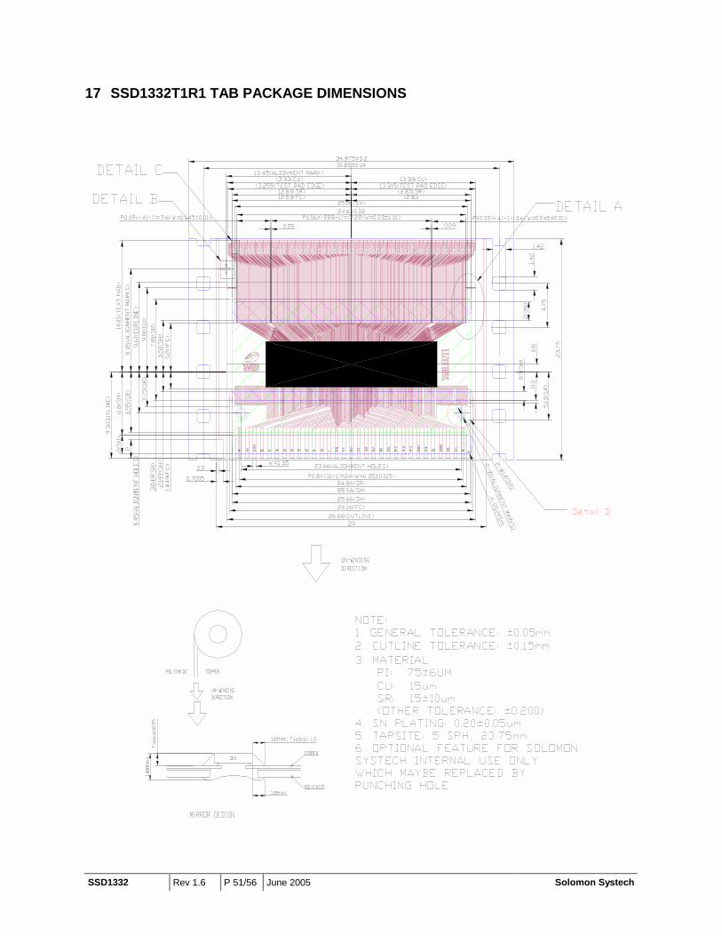
SSD1332 Rev 1.6 P 51/56 June 2005 Solomon Systech
17 SSD1332T1R1 TAB PACKAGE DIMENSIONS
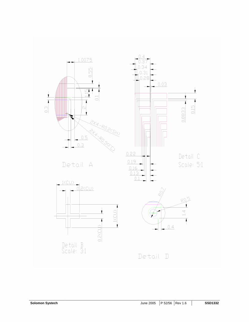
Solomon Systech June 2005 P 52/56 Rev 1.6 SSD1332
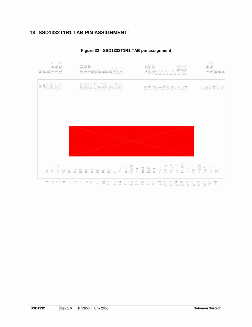
SSD1332 Rev 1.6 P 53/56 June 2005 Solomon Systech
18 SSD1332T1R1 TAB PIN ASSIGNMENT
Figure 32 - SSD1332T1R1 TAB pin assignment

Solomon Systech June 2005 P 54/56 Rev 1.6 SSD1332
Pad.no Pad.name Pad.no Pad.name Pad.no Pad.name Pad.no Pad.name Pad.no Pad.name Pad.no Pad.name Pad.no Pad.name 1 NC 61 COM11 121 SC79 181 SC59 241 SC39 301 SC19 361 NC 2 VCC 62 COM9 122 SB79 182 SB59 242 SB39 302 SB19 362 NC 3 VCOMH 63 COM7 123 SA79 183 SA59 243 SA39 303 SA19 363 NC 4 NC 64 COM5 124 SC78 184 SC58 244 SC38 304 SC18 364 NC 5 D7 65 COM3 125 SB78 185 SB58 245 SB38 305 SB18 365 NC 6 D6 66 COM1 126 SA78 186 SA58 246 SA38 306 SA18 366 NC 7 D5 67 NC 127 SC77 187 SC57 247 SC37 307 SC17 367 COM0 8 D4 68 NC 128 SB77 188 SB57 248 SB37 308 SB17 368 COM2 9 D3 69 NC 129 SA77 189 SA57 249 SA37 309 SA17 369 COM4
10 D2 70 NC 130 SC76 190 SC56 250 SC36 310 SC16 370 COM6 11 D1 71 NC 131 SB76 191 SB56 251 SB36 311 SB16 371 COM8 12 D0 72 NC 132 SA76 192 SA56 252 SA36 312 SA16 372 COM10 13 E 73 SC95 133 SC75 193 SC55 253 SC35 313 SC15 373 COM12 14 R/W 74 SB95 134 SB75 194 SB55 254 SB35 314 SB15 374 COM14 15 D/C 75 SA95 135 SA75 195 SA55 255 SA35 315 SA15 375 COM16 16 RES# 76 SC94 136 SC74 196 SC54 256 SC34 316 SC14 376 COM18 17 CS# 77 SB94 137 SB74 197 SB54 257 SB34 317 SB14 377 COM20 18 IREF 78 SA94 138 SA74 198 SA54 258 SA34 318 SA14 378 COM22 19 BS2 79 SC93 139 SC73 199 SC53 259 SC33 319 SC13 379 COM24 20 BS1 80 SB93 140 SB73 200 SB53 260 SB33 320 SB13 380 COM26 21 VDD 81 SA93 141 SA73 201 SA53 261 SA33 321 SA13 381 COM28 22 VP_C 82 SC92 142 SC72 202 SC52 262 SC32 322 SC12 382 COM30 23 VP_B 83 SB92 143 SB72 203 SB52 263 SB32 323 SB12 383 COM32 24 VP_A 84 SA92 144 SA72 204 SA52 264 SA32 324 SA12 384 COM34 25 BVREF 85 SC91 145 SC71 205 SC51 265 SC31 325 SC11 385 COM36 26 RESE 86 SB91 146 SB71 206 SB51 266 SB31 326 SB11 386 COM38 27 FR 87 SA91 147 SA71 207 SA51 267 SA31 327 SA11 387 COM40 28 VDDB 88 SC90 148 SC70 208 SC50 268 SC30 328 SC10 388 COM42 29 GDR 89 SB90 149 SB70 209 SB50 269 SB30 329 SB10 389 COM44 30 VSS 90 SA90 150 SA70 210 SA50 270 SA30 330 SA10 390 COM46 31 NC 91 SC89 151 SC69 211 SC49 271 SC29 331 SC9 391 COM48 32 NC 92 SB89 152 SB69 212 SB49 272 SB29 332 SB9 392 COM50 33 NC 93 SA89 153 SA69 213 SA49 273 SA29 333 SA9 393 COM52 34 NC 94 SC88 154 SC68 214 SC48 274 SC28 334 SC8 394 COM54 35 COM63 95 SB88 155 SB68 215 SB48 275 SB28 335 SB8 395 COM56 36 COM61 96 SA88 156 SA68 216 SA48 276 SA28 336 SA8 396 COM58 37 COM59 97 SC87 157 SC67 217 SC47 277 SC27 337 SC7 397 COM60 38 COM57 98 SB87 158 SB67 218 SB47 278 SB27 338 SB7 398 COM62 39 COM55 99 SA87 159 SA67 219 SA47 279 SA27 339 SA7 399 NC 40 COM53 100 SC86 160 SC66 220 SC46 280 SC26 340 SC6 400 NC 41 COM51 101 SB86 161 SB66 221 SB46 281 SB26 341 SB6 401 NC 42 COM49 102 SA86 162 SA66 222 SA46 282 SA26 342 SA6 43 COM47 103 SC85 163 SC65 223 SC45 283 SC25 343 SC5 44 COM45 104 SB85 164 SB65 224 SB45 284 SB25 344 SB5 45 COM43 105 SA85 165 SA65 225 SA45 285 SA25 345 SA5 46 COM41 106 SC84 166 SC64 226 SC44 286 SC24 346 SC4 47 COM39 107 SB84 167 SB64 227 SB44 287 SB24 347 SB4 48 COM37 108 SA84 168 SA64 228 SA44 288 SA24 348 SA4 49 COM35 109 SC83 169 SC63 229 SC43 289 SC23 349 SC3 50 COM33 110 SB83 170 SB63 230 SB43 290 SB23 350 SB3 51 COM31 111 SA83 171 SA63 231 SA43 291 SA23 351 SA3 52 COM29 112 SC82 172 SC62 232 SC42 292 SC22 352 SC2 53 COM27 113 SB82 173 SB62 233 SB42 293 SB22 353 SB2 54 COM25 114 SA82 174 SA62 234 SA42 294 SA22 354 SA2 55 COM23 115 SC81 175 SC61 235 SC41 295 SC21 355 SC1 56 COM21 116 SB81 176 SB61 236 SB41 296 SB21 356 SB1 57 COM19 117 SA81 177 SA61 237 SA41 297 SA21 357 SA1 58 COM17 118 SC80 178 SC60 238 SC40 298 SC20 358 SC0 59 COM15 119 SB80 179 SB60 239 SB40 299 SB20 359 SB0 60 COM13 120 SA80 180 SA60 240 SA40 300 SA20 360 SA0
Table 17 - SSD1332T1R1 TAB pin assignment

SSD1332 Rev 1.6 P 55/56 June 2005 Solomon Systech
19 SSD1332Z PACKAGE DETAILS
mm (mil)W1 76.0 +0.2/-0.1 (2992)W2 68.0 +0.2/-0.1 (2677)H 4.20 +/-0.1 (165)Px 20.36 +/-0.1 (802)Py 3.23 +/-0.1 (127)X 15.60 +/- (614)Y 2.10 +/- (83)Z 0.61 +/-0.05 (24)N 80
Spec

Solomon Systech June 2005 P 56/56 Rev 1.6 SSD1332
http://www.solomon-systech.com
Solomon Systech reserves the right to make changes without further notice to any products herein. Solomon Systech makes no warranty,representation or guarantee regarding the suitability of its products for any particular purpose, nor does Solomon Systech assume any liability arisingout of the application or use of any product or circuit, and specifically disclaims any and all liability, including without limitation consequential orincidental damages. “Typical” parameters can and do vary in different applications. All operating parameters, including “Typicals” must be validatedfor each customer application by customer’s technical experts. Solomon Systech does not convey any license under its patent rights nor the rights ofothers. Solomon Systech products are not designed, intended, or authorized for use as components in systems intended for surgical implant into thebody, or other applications intended to support or sustain life, or for any other application in which the failure of the Solomon Systech product couldcreate a situation where personal injury or death may occur. Should Buyer purchase or use Solomon Systech products for any such unintended orunauthorized application, Buyer shall indemnify and hold Solomon Systech and its offices, employees, subsidiaries, affiliates, and distributorsharmless against all claims, costs, damages, and expenses, and reasonable attorney fees arising out of, directly or indirectly, any claim of personalinjury or death associated with such unintended or unauthorized use, even if such claim alleges that Solomon Systech was negligent regarding thedesign or manufacture of the part.