Embed Size (px)
Citation preview
AMC: An Asynchronous Memory CompilerSamira Ataei and Rajit Manohar
Computer Systems Lab, Yale University, New Haven, CT 06520{samira.ataei, rajit.manohar}@yale.edu
Abstract—The lack of electronic design automation (EDA)tools for asynchronous circuits makes it challenging to designasynchronous systems that have high complexity. This restrictionalso makes it almost impossible to prototype and comparenew asynchronous designs with their clocked counterparts. Theavailability of high quality EDA tools would significantly bolsterresearch in asynchronous design, and potentially lead to theiradoption in certain application domains.
This paper presents AMC: an open-source asynchronouspipelined memory compiler. AMC generates SRAM moduleswith a bundled-data datapath and quasi-delay-insensitive control.AMC is a flexible, user-modifiable and technology-independentmemory compiler that generates fabricable SRAM blocks in abroad range of sizes, configurations and process nodes. AMCalso produces memory designs that are competitive with bothasynchronous and synchronous memories in the literature. AMCaims to reduce design turn-around time and amplify the researchin the asynchronous design community.
I. INTRODUCTION
Memory latency is a critical performance bottleneck inhigh-performance digital systems. Data movement betweenmemory and logic (sometimes referred to as the von Neumannbottleneck) largely dominates overall system performance andpower consumption in both general-purpose computing andspecial-purpose architectures for big data computing. Althoughwide busses can improve memory bandwidth at a cost in area,memory latency remains a performance barrier.
Asynchronous SRAM has the potential to improve SRAMlatency and reduce its sensitivity to fabrication variations com-pared to clocked SRAMs. The standard six transistor SRAMbit-cell produces a differential output, making it compatiblewith a dual-rail data encoding that encodes both the presenceand absence of data. Asynchronous SRAMs can alleviatethe timing constraints presented in clocked SRAM, provideshigher throughput through pipelining and overlapping memoryaccesses to different banks, because they naturally handle thevariations in memory read access time. Pipelining overhead inthe asynchronous case can be designed to minimize impact onread latency, permitting asynchronous SRAMs that have bothexcellent latency as well as high throughput.
In modern scaled technologies, memory design is consis-tently one of the most challenging parts of circuit designdue to increasing device variability, higher leakage-powerconsumption, and physical design rule complexity. As a result,the complexity of memory design has dramatically increased.Since most ASICs require some on-chip memory, includingmemory design as part of individual ASIC development wouldsignificantly increase cost. The general practice in industry is
to use a third-party memory compiler to minimize develop-ment costs, enabling design teams to focus on the core ASIC.
Access to a good memory compiler is a major limitation inacademia. Process design kits (PDK) do not include memoryblocks, and commercial compilers are not always accessible.This problem is exacerbated for asynchronous chips in bothacademia and industry, since asynchronous logic is not directlysupported by commercial tools or memory compilers.
In recent years, there have been efforts to provide anopen-source platform to automate memory layout generation.However, the generated memories by most of such platformsare not silicon-verified and are also not competitive with cus-tom designed high-performance memories. Synopsys’ genericmemory compiler [1] only supports Synopsys’ 32/28nm and90nm abstract technologies, which do not correspond to afoundry technology.1 OpenRAM [2], developed through acollaboration between OSU and UCSC, is a synchronousopen-source memory compiler. While OpenRAM provides aflexible and portable platform to implement clocked memories,it doesn’t support thin-cell layout (needed for the designrules at 65nm and below) or modern design rules. Also, theperformance of memories generated by OpenRAM is lowas the sequence of operations needed for memory operation(capturing the address and data bits, address decoding, bitlineprecharging and data driving/sensing) are bounded by clockedges which does not allow memory to perform at its highestfrequency. With only four banks, the biggest 32-bit memorythat can be generated by OpenRAM compiler is 32KB.
This paper presents AMC: an open-source asynchronouspipelined memory compiler. AMC applies techniques frompipelined asynchronous circuit design to improve the average-case performance of memory access and supports non-uniformmemory access time. AMC generates multi-bank SRAM mod-ules, using a combination of quasi delay-insensitive (QDI)control and bundled-data datapath. The largest 32-bit memorythat can be generated by AMC is 1 MB. AMC supports anatomic read-modify-write operation in addition to the readand write memory operations that has a longer cycle timecompared to read/write operations, exploiting the ability ofasynchronous circuits to handle data-dependent delay. AMCleverages the micro-architectural techniques introduced by thecache of an asynchronous MIPS processor [3], and inheritsthe data structures and base functions from the OpenRAMcompiler [2]. Like OpenRAM, the back end GDSII frame-
1This enables them to provide the technology information without involvingcomplex foundry non-disclosure agreements.
Row
-Dec
oder
Sub-
Bank
D
ecod
erC
ontro
l Circ
uitry
Sub-
Bank
#2
Sub-
Bank
#N
Sub-
Bank
#1
Bank
D
ecod
erC
ontro
l C
ircui
try
Bank #2
Bank #N
Bank #1
DoutDinA
ddr&
Ctr
l
Split and Merge Arrays
wreqwack rack rreqre
qac
k
PrechargerWrite-Completion
Read-Completion
Sense AmplifierWrite Driver
Bitline Multiplexer
Wor
dlin
eD
river
Con
trol D
river
6T Array
6TWordline
Bitl
ine
Bitl
ine_
Bar
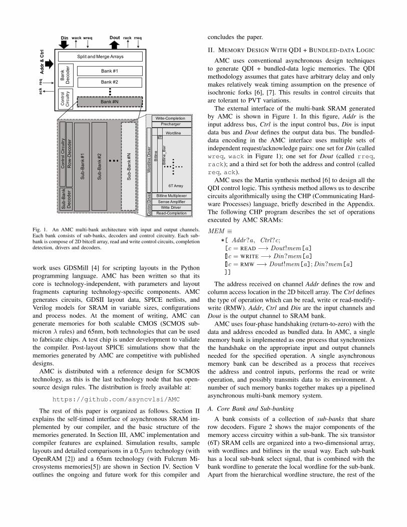
Fig. 1. An AMC multi-bank architecture with input and output channels.Each bank consists of sub-banks, decoders and control circuitry. Each sub-bank is compose of 2D bitcell array, read and write control circuits, completiondetection, drivers and decoders.
work uses GDSMill [4] for scripting layouts in the Pythonprogramming language. AMC has been written so that itscore is technology-independent, with parameters and layoutfragments capturing technology-specific components. AMCgenerates circuits, GDSII layout data, SPICE netlists, andVerilog models for SRAM in variable sizes, configurationsand process nodes. At the moment of writing, AMC cangenerate memories for both scalable CMOS (SCMOS sub-micron λ rules) and 65nm, both technologies that can be usedto fabricate chips. A test chip is under development to validatethe compiler. Post-layout SPICE simulations show that thememories generated by AMC are competitive with publisheddesigns.
AMC is distributed with a reference design for SCMOStechnology, as this is the last technology node that has open-source design rules. The distribution is freely available at:
https://github.com/asyncvlsi/AMC
The rest of this paper is organized as follows. Section IIexplains the self-timed interface of asynchronous SRAM im-plemented by our compiler, and the basic structure of thememories generated. In Section III, AMC implementation andcompiler features are explained. Simulation results, samplelayouts and detailed comparisons in a 0.5µm technology (withOpenRAM [2]) and a 65nm technology (with Fulcrum Mi-crosystems memories[5]) are shown in Section IV. Section Voutlines the ongoing and future work for this compiler and
concludes the paper.
II. MEMORY DESIGN WITH QDI + BUNDLED-DATA LOGIC
AMC uses conventional asynchronous design techniquesto generate QDI + bundled-data logic memories. The QDImethodology assumes that gates have arbitrary delay and onlymakes relatively weak timing assumption on the presence ofisochronic forks [6], [7]. This results in control circuits thatare tolerant to PVT variations.
The external interface of the multi-bank SRAM generatedby AMC is shown in Figure 1. In this figure, Addr is theinput address bus, Ctrl is the input control bus, Din is inputdata bus and Dout defines the output data bus. The bundled-data encoding in the AMC interface uses multiple sets ofindependent request/acknowledge pairs: one set for Din (calledwreq, wack in Figure 1); one set for Dout (called rreq,rack); and a third set for both the address and control (calledreq, ack).
AMC uses the Martin synthesis method [6] to design all theQDI control logic. This synthesis method allows us to describecircuits algorithmically using the CHP (Communicating Hard-ware Processes) language, briefly described in the Appendix.The following CHP program describes the set of operationsexecuted by AMC SRAMs:
MEM ≡*[ Addr?a, Ctrl?c;[c = READ −→ Dout !mem[a][]c = WRITE −→ Din?mem[a][]c = RMW −→ Dout !mem[a];Din?mem[a]]]
The address received on channel Addr defines the row andcolumn access location in the 2D bitcell array. The Ctrl definesthe type of operation which can be read, write or read-modify-write (RMW). Addr, Ctrl and Din are the input channels andDout is the output channel to SRAM bank.
AMC uses four-phase handshaking (return-to-zero) with thedata and address encoded as bundled data. In AMC, a singlememory bank is implemented as one process that synchronizesthe handshake on the appropriate input and output channelsneeded for the specified operation. A single asynchronousmemory bank can be described as a process that receivesthe address and control inputs, performs the read or writeoperation, and possibly transmits data to its environment. Anumber of such memory banks together makes up a pipelinedasynchronous multi-bank memory system.
A. Core Bank and Sub-banking
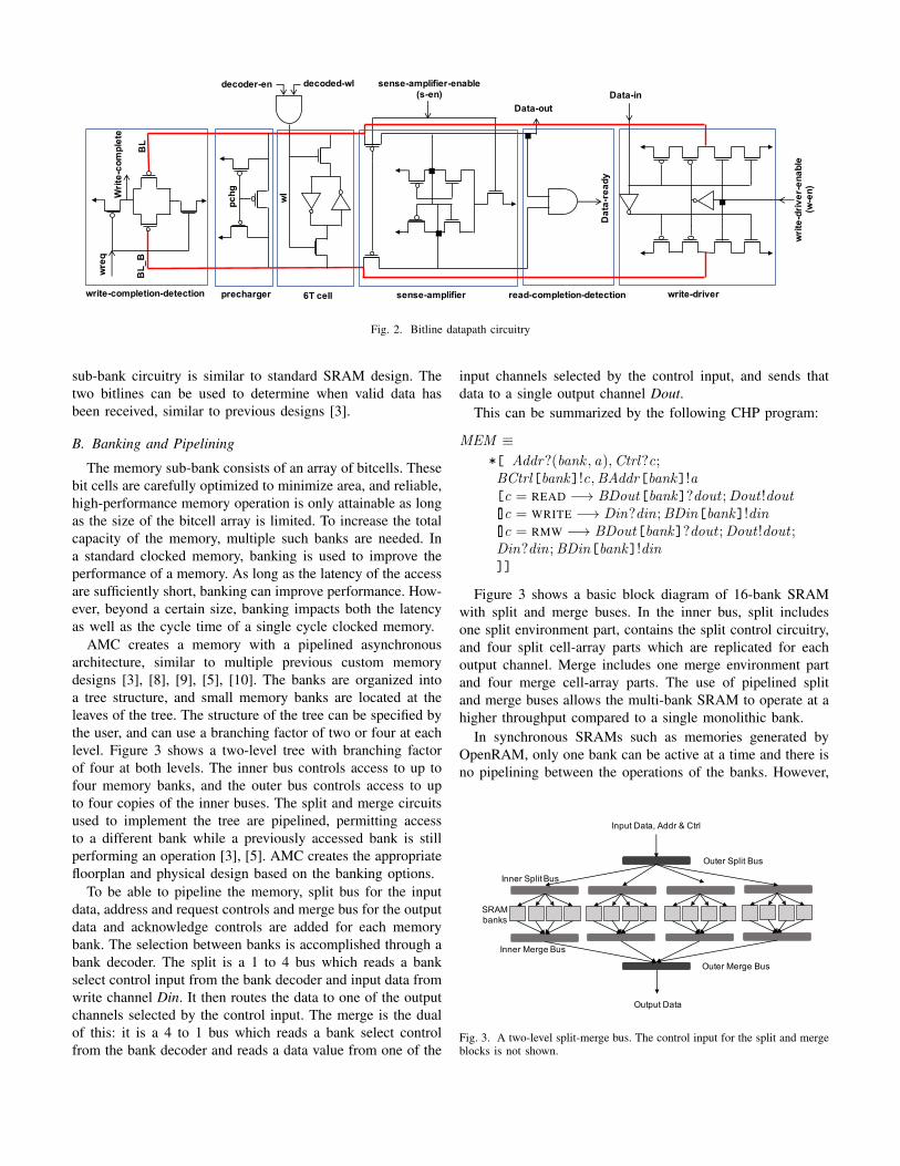
A bank consists of a collection of sub-banks that sharerow decoders. Figure 2 shows the major components of thememory access circuitry within a sub-bank. The six transistor(6T) SRAM cells are organized into a two-dimensional array,with wordlines and bitlines in the usual way. Each sub-bankhas a local sub-bank select signal, that is combined with thebank wordline to generate the local wordline for the sub-bank.Apart from the hierarchical wordline structure, the rest of the
BL
BL_
B
Writ
e-co
mpl
ete
wre
q
write-completion-detection read-completion-detection
sense-amplifier-enable (s-en)
Dat
a-re
ady
Data-out
..
.
sense-amplifier
.
writ
e-dr
iver
-ena
ble
(w-e
n)
Data-in
write-driverprechargerw
l
decoder-en decoded-wl
6T cell
pchg
Fig. 2. Bitline datapath circuitry
sub-bank circuitry is similar to standard SRAM design. Thetwo bitlines can be used to determine when valid data hasbeen received, similar to previous designs [3].
B. Banking and Pipelining
The memory sub-bank consists of an array of bitcells. Thesebit cells are carefully optimized to minimize area, and reliable,high-performance memory operation is only attainable as longas the size of the bitcell array is limited. To increase the totalcapacity of the memory, multiple such banks are needed. Ina standard clocked memory, banking is used to improve theperformance of a memory. As long as the latency of the accessare sufficiently short, banking can improve performance. How-ever, beyond a certain size, banking impacts both the latencyas well as the cycle time of a single cycle clocked memory.
AMC creates a memory with a pipelined asynchronousarchitecture, similar to multiple previous custom memorydesigns [3], [8], [9], [5], [10]. The banks are organized intoa tree structure, and small memory banks are located at theleaves of the tree. The structure of the tree can be specified bythe user, and can use a branching factor of two or four at eachlevel. Figure 3 shows a two-level tree with branching factorof four at both levels. The inner bus controls access to up tofour memory banks, and the outer bus controls access to upto four copies of the inner buses. The split and merge circuitsused to implement the tree are pipelined, permitting accessto a different bank while a previously accessed bank is stillperforming an operation [3], [5]. AMC creates the appropriatefloorplan and physical design based on the banking options.
To be able to pipeline the memory, split bus for the inputdata, address and request controls and merge bus for the outputdata and acknowledge controls are added for each memorybank. The selection between banks is accomplished through abank decoder. The split is a 1 to 4 bus which reads a bankselect control input from the bank decoder and input data fromwrite channel Din. It then routes the data to one of the outputchannels selected by the control input. The merge is the dualof this: it is a 4 to 1 bus which reads a bank select controlfrom the bank decoder and reads a data value from one of the
input channels selected by the control input, and sends thatdata to a single output channel Dout.
This can be summarized by the following CHP program:
MEM ≡*[ Addr?(bank , a),Ctrl?c;BCtrl[bank]!c,BAddr[bank]!a[c = READ −→ BDout[bank]?dout ;Dout !dout[]c = WRITE −→ Din?din;BDin[bank]!din[]c = RMW −→ BDout[bank]?dout ;Dout !dout ;Din?din;BDin[bank]!din]]
Figure 3 shows a basic block diagram of 16-bank SRAMwith split and merge buses. In the inner bus, split includesone split environment part, contains the split control circuitry,and four split cell-array parts which are replicated for eachoutput channel. Merge includes one merge environment partand four merge cell-array parts. The use of pipelined splitand merge buses allows the multi-bank SRAM to operate at ahigher throughput compared to a single monolithic bank.
In synchronous SRAMs such as memories generated byOpenRAM, only one bank can be active at a time and there isno pipelining between the operations of the banks. However,
Input Data, Addr & Ctrl
Outer Split Bus
Outer Merge Bus
Inner Split Bus
Inner Merge Bus
SRAM banks
Output Data
Fig. 3. A two-level split-merge bus. The control input for the split and mergeblocks is not shown.
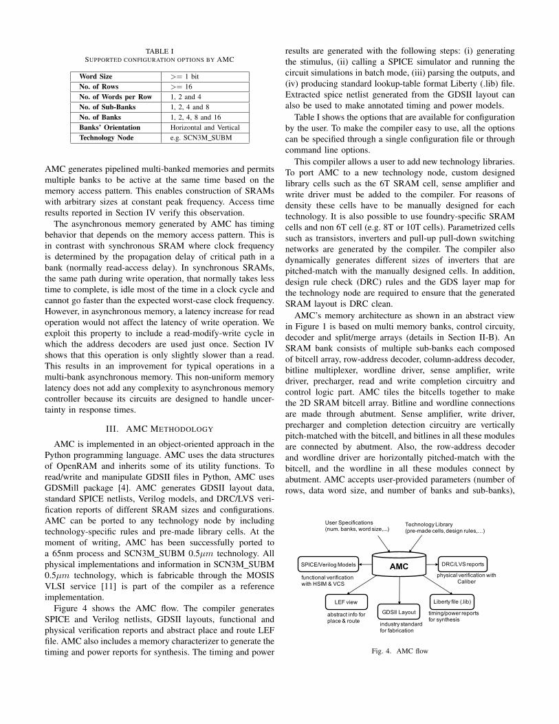
TABLE ISUPPORTED CONFIGURATION OPTIONS BY AMC
Word Size >= 1 bitNo. of Rows >= 16No. of Words per Row 1, 2 and 4No. of Sub-Banks 1, 2, 4 and 8No. of Banks 1, 2, 4, 8 and 16Banks’ Orientation Horizontal and VerticalTechnology Node e.g. SCN3M SUBM
AMC generates pipelined multi-banked memories and permitsmultiple banks to be active at the same time based on thememory access pattern. This enables construction of SRAMswith arbitrary sizes at constant peak frequency. Access timeresults reported in Section IV verify this observation.
The asynchronous memory generated by AMC has timingbehavior that depends on the memory access pattern. This isin contrast with synchronous SRAM where clock frequencyis determined by the propagation delay of critical path in abank (normally read-access delay). In synchronous SRAMs,the same path during write operation, that normally takes lesstime to complete, is idle most of the time in a clock cycle andcannot go faster than the expected worst-case clock frequency.However, in asynchronous memory, a latency increase for readoperation would not affect the latency of write operation. Weexploit this property to include a read-modify-write cycle inwhich the address decoders are used just once. Section IVshows that this operation is only slightly slower than a read.This results in an improvement for typical operations in amulti-bank asynchronous memory. This non-uniform memorylatency does not add any complexity to asynchronous memorycontroller because its circuits are designed to handle uncer-tainty in response times.
III. AMC METHODOLOGY
AMC is implemented in an object-oriented approach in thePython programming language. AMC uses the data structuresof OpenRAM and inherits some of its utility functions. Toread/write and manipulate GDSII files in Python, AMC usesGDSMill package [4]. AMC generates GDSII layout data,standard SPICE netlists, Verilog models, and DRC/LVS veri-fication reports of different SRAM sizes and configurations.AMC can be ported to any technology node by includingtechnology-specific rules and pre-made library cells. At themoment of writing, AMC has been successfully ported toa 65nm process and SCN3M SUBM 0.5µm technology. Allphysical implementations and information in SCN3M SUBM0.5µm technology, which is fabricable through the MOSISVLSI service [11] is part of the compiler as a referenceimplementation.
Figure 4 shows the AMC flow. The compiler generatesSPICE and Verilog netlists, GDSII layouts, functional andphysical verification reports and abstract place and route LEFfile. AMC also includes a memory characterizer to generate thetiming and power reports for synthesis. The timing and power
results are generated with the following steps: (i) generatingthe stimulus, (ii) calling a SPICE simulator and running thecircuit simulations in batch mode, (iii) parsing the outputs, and(iv) producing standard lookup-table format Liberty (.lib) file.Extracted spice netlist generated from the GDSII layout canalso be used to make annotated timing and power models.
Table I shows the options that are available for configurationby the user. To make the compiler easy to use, all the optionscan be specified through a single configuration file or throughcommand line options.
This compiler allows a user to add new technology libraries.To port AMC to a new technology node, custom designedlibrary cells such as the 6T SRAM cell, sense amplifier andwrite driver must be added to the compiler. For reasons ofdensity these cells have to be manually designed for eachtechnology. It is also possible to use foundry-specific SRAMcells and non 6T cell (e.g. 8T or 10T cells). Parametrized cellssuch as transistors, inverters and pull-up pull-down switchingnetworks are generated by the compiler. The compiler alsodynamically generates different sizes of inverters that arepitched-match with the manually designed cells. In addition,design rule check (DRC) rules and the GDS layer map forthe technology node are required to ensure that the generatedSRAM layout is DRC clean.
AMC’s memory architecture as shown in an abstract viewin Figure 1 is based on multi memory banks, control circuity,decoder and split/merge arrays (details in Section II-B). AnSRAM bank consists of multiple sub-banks each composedof bitcell array, row-address decoder, column-address decoder,bitline multiplexer, wordline driver, sense amplifier, writedriver, precharger, read and write completion circuitry andcontrol logic part. AMC tiles the bitcells together to makethe 2D SRAM bitcell array. Bitline and wordline connectionsare made through abutment. Sense amplifier, write driver,precharger and completion detection circuitry are verticallypitch-matched with the bitcell, and bitlines in all these modulesare connected by abutment. Also, the row-address decoderand wordline driver are horizontally pitched-match with thebitcell, and the wordline in all these modules connect byabutment. AMC accepts user-provided parameters (number ofrows, data word size, and number of banks and sub-banks),
User Specifications (num. banks, word size,...)
Technology Library(pre-made cells, design rules,…)
industry standard for fabrication
GDSII Layoutabstract info for place & route
LEF view
functional verificationwith HSIM & VCS
SPICE/Verilog Models
physical verification with Caliber
DRC/LVS reports
timing/power reportsfor synthesis
Liberty file (.lib)
AMC
Fig. 4. AMC flow
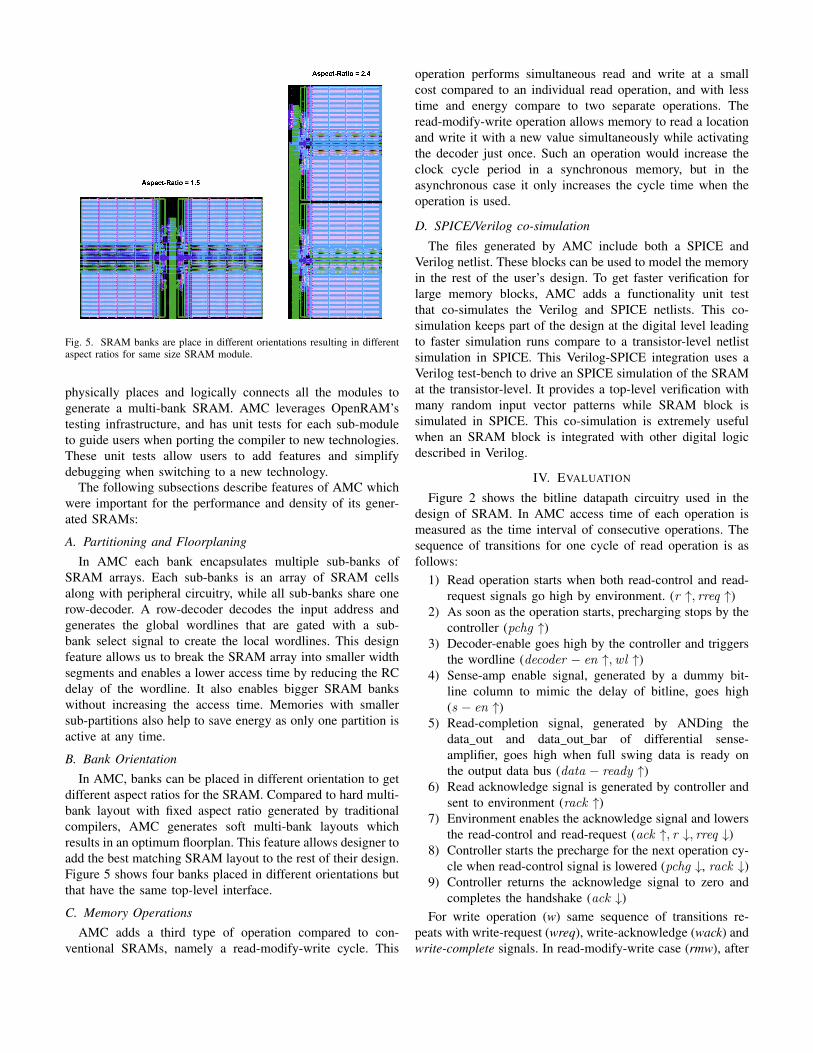
Fig. 5. SRAM banks are place in different orientations resulting in differentaspect ratios for same size SRAM module.
physically places and logically connects all the modules togenerate a multi-bank SRAM. AMC leverages OpenRAM’stesting infrastructure, and has unit tests for each sub-moduleto guide users when porting the compiler to new technologies.These unit tests allow users to add features and simplifydebugging when switching to a new technology.
The following subsections describe features of AMC whichwere important for the performance and density of its gener-ated SRAMs:
A. Partitioning and FloorplaningIn AMC each bank encapsulates multiple sub-banks of
SRAM arrays. Each sub-banks is an array of SRAM cellsalong with peripheral circuitry, while all sub-banks share onerow-decoder. A row-decoder decodes the input address andgenerates the global wordlines that are gated with a sub-bank select signal to create the local wordlines. This designfeature allows us to break the SRAM array into smaller widthsegments and enables a lower access time by reducing the RCdelay of the wordline. It also enables bigger SRAM bankswithout increasing the access time. Memories with smallersub-partitions also help to save energy as only one partition isactive at any time.
B. Bank OrientationIn AMC, banks can be placed in different orientation to get
different aspect ratios for the SRAM. Compared to hard multi-bank layout with fixed aspect ratio generated by traditionalcompilers, AMC generates soft multi-bank layouts whichresults in an optimum floorplan. This feature allows designer toadd the best matching SRAM layout to the rest of their design.Figure 5 shows four banks placed in different orientations butthat have the same top-level interface.
C. Memory OperationsAMC adds a third type of operation compared to con-
ventional SRAMs, namely a read-modify-write cycle. This
operation performs simultaneous read and write at a smallcost compared to an individual read operation, and with lesstime and energy compare to two separate operations. Theread-modify-write operation allows memory to read a locationand write it with a new value simultaneously while activatingthe decoder just once. Such an operation would increase theclock cycle period in a synchronous memory, but in theasynchronous case it only increases the cycle time when theoperation is used.
D. SPICE/Verilog co-simulation
The files generated by AMC include both a SPICE andVerilog netlist. These blocks can be used to model the memoryin the rest of the user’s design. To get faster verification forlarge memory blocks, AMC adds a functionality unit testthat co-simulates the Verilog and SPICE netlists. This co-simulation keeps part of the design at the digital level leadingto faster simulation runs compare to a transistor-level netlistsimulation in SPICE. This Verilog-SPICE integration uses aVerilog test-bench to drive an SPICE simulation of the SRAMat the transistor-level. It provides a top-level verification withmany random input vector patterns while SRAM block issimulated in SPICE. This co-simulation is extremely usefulwhen an SRAM block is integrated with other digital logicdescribed in Verilog.
IV. EVALUATION
Figure 2 shows the bitline datapath circuitry used in thedesign of SRAM. In AMC access time of each operation ismeasured as the time interval of consecutive operations. Thesequence of transitions for one cycle of read operation is asfollows:
1) Read operation starts when both read-control and read-request signals go high by environment. (r ↑, rreq ↑)
2) As soon as the operation starts, precharging stops by thecontroller (pchg ↑)
3) Decoder-enable goes high by the controller and triggersthe wordline (decoder − en ↑,wl ↑)
4) Sense-amp enable signal, generated by a dummy bit-line column to mimic the delay of bitline, goes high(s − en ↑)
5) Read-completion signal, generated by ANDing thedata out and data out bar of differential sense-amplifier, goes high when full swing data is ready onthe output data bus (data − ready ↑)
6) Read acknowledge signal is generated by controller andsent to environment (rack ↑)
7) Environment enables the acknowledge signal and lowersthe read-control and read-request (ack ↑, r ↓, rreq ↓)
8) Controller starts the precharge for the next operation cy-cle when read-control signal is lowered (pchg ↓, rack ↓)
9) Controller returns the acknowledge signal to zero andcompletes the handshake (ack ↓)
For write operation (w) same sequence of transitions re-peats with write-request (wreq), write-acknowledge (wack) andwrite-complete signals. In read-modify-write case (rmw), after
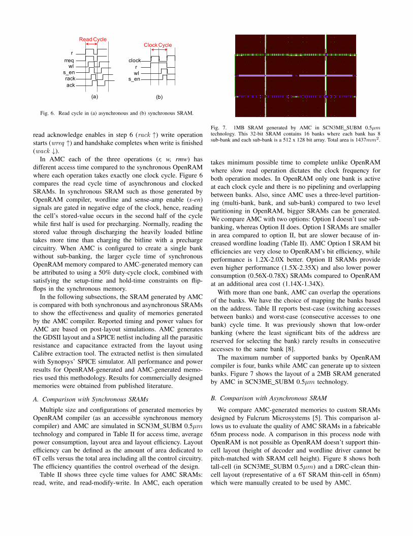
rrreq
wls_enrackack
Read Cycle
rwl
s_en
Clock Cycle
clock
(a) (b)
Fig. 6. Read cycle in (a) asynchronous and (b) synchronous SRAM.
read acknowledge enables in step 6 (rack ↑) write operationstarts (wreq ↑) and handshake completes when write is finished(wack ↓).
In AMC each of the three operations (r, w, rmw) hasdifferent access time compared to the synchronous OpenRAMwhere each operation takes exactly one clock cycle. Figure 6compares the read cycle time of asynchronous and clockedSRAMs. In synchronous SRAM such as those generated byOpenRAM compiler, wordline and sense-amp enable (s-en)signals are gated in negative edge of the clock, hence, readingthe cell’s stored-value occurs in the second half of the cyclewhile first half is used for precharging. Normally, reading thestored value through discharging the heavily loaded bitlinetakes more time than charging the bitline with a prechargecircuitry. When AMC is configured to create a single bankwithout sub-banking, the larger cycle time of synchronousOpenRAM memory compared to AMC-generated memory canbe attributed to using a 50% duty-cycle clock, combined withsatisfying the setup-time and hold-time constraints on flip-flops in the synchronous memory.
In the following subsections, the SRAM generated by AMCis compared with both synchronous and asynchronous SRAMsto show the effectiveness and quality of memories generatedby the AMC compiler. Reported timing and power values forAMC are based on post-layout simulations. AMC generatesthe GDSII layout and a SPICE netlist including all the parasiticresistance and capacitance extracted from the layout usingCalibre extraction tool. The extracted netlist is then simulatedwith Synopsys’ SPICE simulator. All performance and powerresults for OpenRAM-generated and AMC-generated memo-ries used this methodology. Results for commercially designedmemories were obtained from published literature.
A. Comparison with Synchronous SRAMs
Multiple size and configurations of generated memories byOpenRAM compiler (as an accessible synchronous memorycompiler) and AMC are simulated in SCN3M SUBM 0.5µmtechnology and compared in Table II for access time, averagepower consumption, layout area and layout efficiency. Layoutefficiency can be defined as the amount of area dedicated to6T cells versus the total area including all the control circuitry.The efficiency quantifies the control overhead of the design.
Table II shows three cycle time values for AMC SRAMs:read, write, and read-modify-write. In AMC, each operation
Fig. 7. 1MB SRAM generated by AMC in SCN3ME SUBM 0.5µmtechnology. This 32-bit SRAM contains 16 banks where each bank has 8sub-bank and each sub-bank is a 512 x 128 bit array. Total area is 1437mm2.
takes minimum possible time to complete unlike OpenRAMwhere slow read operation dictates the clock frequency forboth operation modes. In OpenRAM only one bank is activeat each clock cycle and there is no pipelining and overlappingbetween banks. Also, since AMC uses a three-level partition-ing (multi-bank, bank, and sub-bank) compared to two levelpartitioning in OpenRAM, bigger SRAMs can be generated.We compare AMC with two options: Option I doesn’t use sub-banking, whereas Option II does. Option I SRAMs are smallerin area compared to option II, but are slower because of in-creased wordline loading (Table II). AMC Option I SRAM bitefficiencies are very close to OpenRAM’s bit efficiency, whileperformance is 1.2X-2.0X better. Option II SRAMs provideeven higher performance (1.5X-2.35X) and also lower powerconsumption (0.56X-0.78X) SRAMs compared to OpenRAMat an additional area cost (1.14X-1.34X).
With more than one bank, AMC can overlap the operationsof the banks. We have the choice of mapping the banks basedon the address. Table II reports best-case (switching accessesbetween banks) and worst-case (consecutive accesses to onebank) cycle time. It was previously shown that low-orderbanking (where the least significant bits of the address arereserved for selecting the bank) rarely results in consecutiveaccesses to the same bank [8].
The maximum number of supported banks by OpenRAMcompiler is four, banks while AMC can generate up to sixteenbanks. Figure 7 shows the layout of a 2MB SRAM generatedby AMC in SCN3ME SUBM 0.5µm technology.
B. Comparison with Asynchronous SRAM
We compare AMC-generated memories to custom SRAMsdesigned by Fulcrum Microsystems [5]. This comparison al-lows us to evaluate the quality of AMC SRAMs in a fabricable65nm process node. A comparison in this process node withOpenRAM is not possible as OpenRAM doesn’t support thin-cell layout (height of decoder and wordline driver cannot bepitch-matched with SRAM cell height). Figure 8 shows bothtall-cell (in SCN3ME SUBM 0.5µm) and a DRC-clean thin-cell layout (representative of a 6T SRAM thin-cell in 65nm)which were manually created to be used by AMC.
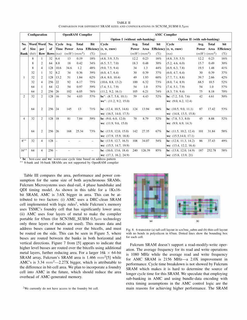
TABLE IICOMPARISON FOR DIFFERENT SRAM SIZES AND CONFIGURATIONS IN SCN3M SUBM 0.5µm
Configuration OpenRAM Compiler AMC CompilerOption I (without sub-banking) Option II (with sub-banking)
No. Word Word No. Cycle Avg. Total Bit Cycle Avg. Total bit Cycle Avg. Total bitof Size per of Time Power Area Efficiency (r, w, rmw) Power Area Efficiency (r, w, rmw) Power Area Efficiency
Bank (bit) Row Rows (ns) (mW ) (mm2) (%) (ns) (mW ) (mm2) (%) (ns) (mW ) (mm2) (%)
8 1 32 6.4 13 0.19 18% (4.8, 3.9, 5.5) 12.2 0.23 16% (4.8, 3.9, 5.5) 12.2 0.23 16%8 2 64 8.8 18 0.42 34% (6.5, 5.7, 7.0) 18.3 0.48 30% (5.2, 4.6, 6.0) 15.7 0.49 30%8 4 128 10.6 34.6 1.2 48% (9.0, 7.5, 9.4) 34 1.3 44% (6.9, 6.3, 7.8) 19.5 1.48 41%
32 1 32 8.2 34 0.36 39% (6.0, 4.7, 6.4) 30 0.39 37% (6.0, 4.7, 6.4) 30 0.39 37%1 32 2 128 13.2 51 1.84 62% (8.4, 8.0, 10.4) 49 1.93 60% (7.7, 7.1, 8.8) 39.7 2.66 42%
32 4 256 22 92 6.17 75% (10.6, 8.8, 13.2) 100 6.32 73% (8.0, 7.4, 8.9) 68.5 10.5 52%64 1 64 12 54 0.97 59% (7.4, 5.1, 7.9) 54 1.0 57% (7.4, 5.1, 7.9) 54 1.0 57%64 2 256 26 102 6.05 76% (11.2, 9.2, 16.1) 105 6.21 74% (8.3, 7.9, 9.4) 75 8.18 70%
2 32 2 128 16 54 4.03 57% bc∗: (8.7, 5.8, 10.1) 59 4.43 52% bc: (7.2, 5.0, 7.6) 42 4.61 50%wc∗: (11.2, 9.2, 15.0) wc: (9.0, 6.2, 12.4)
64 2 256 24 145 13 71% bc: (12.4, 10.5, 14.6) 124 13.94 66% bc: (10.5, 9.0, 11.1) 87 17.42 53%wc: (16.5, 14.0, 17.5) wc: (14.8, 13.5, 15.8)
4 32 2 128 18 81 7.84 59% bc: (9.0, 6.0, 12.0) 70 8.79 52% bc: (7.8, 5.3, 8.0) 45 8.88 52%wc: (11.9, 9.6, 15.0) wc: (9.9, 6.9, 14.3)
64 2 256 26 168 25.34 73% bc: (13.9, 12.0, 15.0) 142 27.35 67% bc: (11.5, 10.2, 12.4) 101 31.84 58%wc: (17.9, 15.9, 18.8) wc: (15.5,14.0, 17.1)
8∗∗ 32 4 128 – – – – bc: (13.9, 12.7, 16.5) 108 34.07 54% bc: (12.8, 11.3, 14.2) 86 37.43 49%wc: (15.5, 14.7, 19.9) wc: (13.4, 12.2, 16.4)
16∗∗ 64 4 256 – – – – bc: (16.0, 13.6, 18.4) 240 126.39 85% bc: (13.8, 12.0, 14.9) 187 252.78 58%wc: (17.3, 16.2, 24.9) wc: (15.8, 13.9, 21)
∗ bc : best-case and wc: worst-case cycle time based on address pattern∗∗ 8-bank and 16-bank SRAMs are not supported by OpenRAM compiler
Table III compares the area, performance and power con-sumption for the same size of both asynchronous SRAMs.Fulcrum Microsystems uses dual-rail, 4 phase handshake andQDI timing model. As shown in this table for a 1Kx16-bit SRAM, AMC is 3.6X bigger in area. This can be at-tributed to two factors: (i) AMC uses a DRC-clean SRAMcell implemented with logic rules2, while Fulcrum’s memoryuses TSMC’s foundry cell that has significantly lower area;(ii) AMC uses four layers of metal to make the compilerportable for 65nm (for SCN3ME SUBM 0.5µm technologyonly three layers of metals are used). This means data andaddress buses cannot be routed over the bitcells, and mustbe routed on the side. This can be seen in Figure 5, wherebuses are routed between the banks in both horizontal andvertical directions. Figure 7 from [5] appears to indicate thathigher level busses are routed over the bitcells using additionalmetal layers, further reducing area. For a larger 16k × 64-bitSRAM array, Fulcrum’s SRAM area is 1.466 mm2[5] whileAMC’s is 3.34 mm2—2.27X bigger, which is attributable tothe difference in bit-cell area. We plan to incorporate a foundrycell into AMC in the future, which should reduce the areaoverhead of AMC-generated memory.
2We currently do not have access to the foundry bit cell.
Fig. 8. 6-transistor (a) tall-cell layout in scn3me subm and (b) thin-cell layoutwith no bends in polysilicon in 65nm. Dotted lines show the bounding boxfor each cell.
Fulcrum SRAM doesn’t support a read-modify-write oper-ation. The average frequency for its read and write operationsis 1080 MHz while the average read and write frequencyfor AMC SRAM is 2156 MHz—a 2.0X improvement inperformance. Cycle time breakdown is not showed by FulcrumSRAM which makes it is hard to determine the source oflonger cycle time for this SRAM. We speculate that employingsub-banking in AMC and using bundle-data encoding withextra timing assumptions in the AMC control logic are themain reasons for achieving higher performance. The SRAM
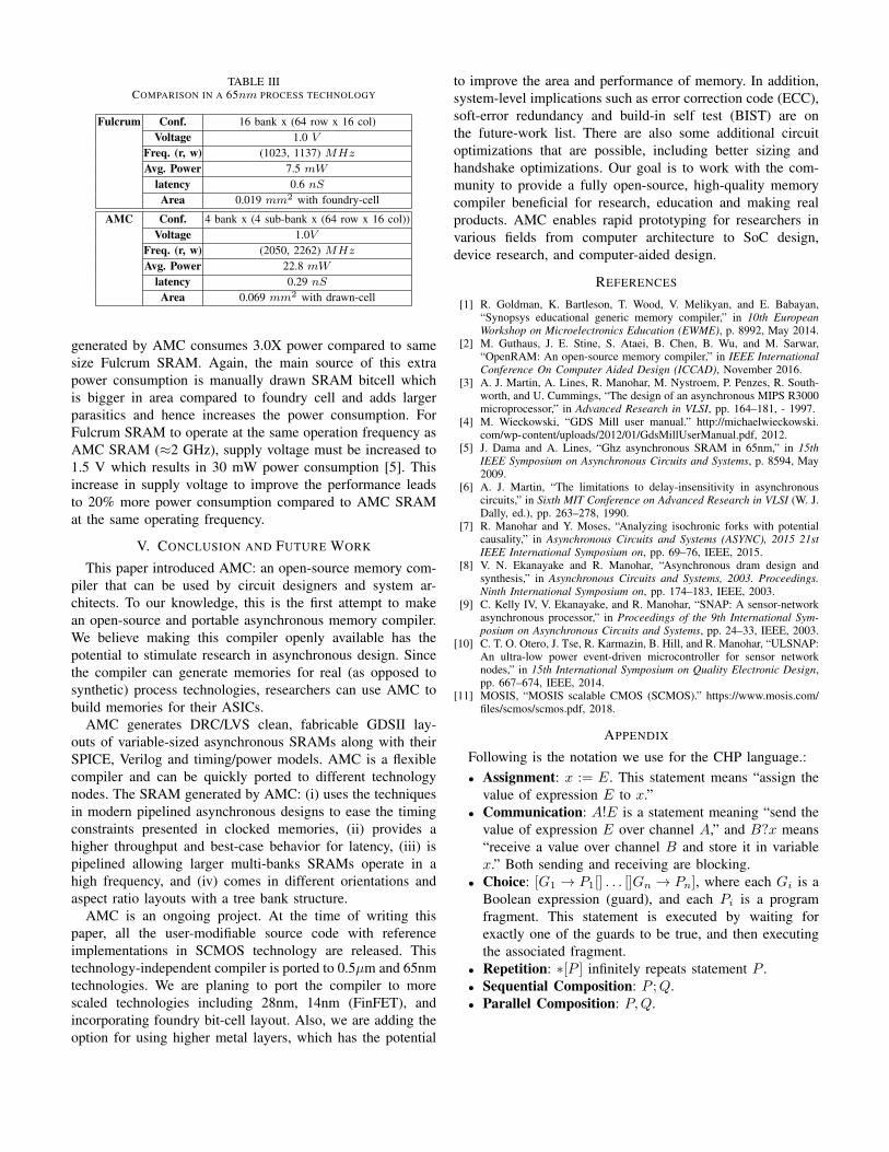
TABLE IIICOMPARISON IN A 65nm PROCESS TECHNOLOGY
Fulcrum Conf. 16 bank x (64 row x 16 col)Voltage 1.0 V
Freq. (r, w) (1023, 1137) MHz
Avg. Power 7.5 mWlatency 0.6 nSArea 0.019 mm2 with foundry-cell
AMC Conf. 4 bank x (4 sub-bank x (64 row x 16 col))Voltage 1.0V
Freq. (r, w) (2050, 2262) MHz
Avg. Power 22.8 mWlatency 0.29 nSArea 0.069 mm2 with drawn-cell
generated by AMC consumes 3.0X power compared to samesize Fulcrum SRAM. Again, the main source of this extrapower consumption is manually drawn SRAM bitcell whichis bigger in area compared to foundry cell and adds largerparasitics and hence increases the power consumption. ForFulcrum SRAM to operate at the same operation frequency asAMC SRAM (≈2 GHz), supply voltage must be increased to1.5 V which results in 30 mW power consumption [5]. Thisincrease in supply voltage to improve the performance leadsto 20% more power consumption compared to AMC SRAMat the same operating frequency.
V. CONCLUSION AND FUTURE WORK
This paper introduced AMC: an open-source memory com-piler that can be used by circuit designers and system ar-chitects. To our knowledge, this is the first attempt to makean open-source and portable asynchronous memory compiler.We believe making this compiler openly available has thepotential to stimulate research in asynchronous design. Sincethe compiler can generate memories for real (as opposed tosynthetic) process technologies, researchers can use AMC tobuild memories for their ASICs.
AMC generates DRC/LVS clean, fabricable GDSII lay-outs of variable-sized asynchronous SRAMs along with theirSPICE, Verilog and timing/power models. AMC is a flexiblecompiler and can be quickly ported to different technologynodes. The SRAM generated by AMC: (i) uses the techniquesin modern pipelined asynchronous designs to ease the timingconstraints presented in clocked memories, (ii) provides ahigher throughput and best-case behavior for latency, (iii) ispipelined allowing larger multi-banks SRAMs operate in ahigh frequency, and (iv) comes in different orientations andaspect ratio layouts with a tree bank structure.
AMC is an ongoing project. At the time of writing thispaper, all the user-modifiable source code with referenceimplementations in SCMOS technology are released. Thistechnology-independent compiler is ported to 0.5µm and 65nmtechnologies. We are planing to port the compiler to morescaled technologies including 28nm, 14nm (FinFET), andincorporating foundry bit-cell layout. Also, we are adding theoption for using higher metal layers, which has the potential
to improve the area and performance of memory. In addition,system-level implications such as error correction code (ECC),soft-error redundancy and build-in self test (BIST) are onthe future-work list. There are also some additional circuitoptimizations that are possible, including better sizing andhandshake optimizations. Our goal is to work with the com-munity to provide a fully open-source, high-quality memorycompiler beneficial for research, education and making realproducts. AMC enables rapid prototyping for researchers invarious fields from computer architecture to SoC design,device research, and computer-aided design.
REFERENCES
[1] R. Goldman, K. Bartleson, T. Wood, V. Melikyan, and E. Babayan,“Synopsys educational generic memory compiler,” in 10th EuropeanWorkshop on Microelectronics Education (EWME), p. 8992, May 2014.
[2] M. Guthaus, J. E. Stine, S. Ataei, B. Chen, B. Wu, and M. Sarwar,“OpenRAM: An open-source memory compiler,” in IEEE InternationalConference On Computer Aided Design (ICCAD), November 2016.
[3] A. J. Martin, A. Lines, R. Manohar, M. Nystroem, P. Penzes, R. South-worth, and U. Cummings, “The design of an asynchronous MIPS R3000microprocessor,” in Advanced Research in VLSI, pp. 164–181, - 1997.
[4] M. Wieckowski, “GDS Mill user manual.” http://michaelwieckowski.com/wp-content/uploads/2012/01/GdsMillUserManual.pdf, 2012.
[5] J. Dama and A. Lines, “Ghz asynchronous SRAM in 65nm,” in 15thIEEE Symposium on Asynchronous Circuits and Systems, p. 8594, May2009.
[6] A. J. Martin, “The limitations to delay-insensitivity in asynchronouscircuits,” in Sixth MIT Conference on Advanced Research in VLSI (W. J.Dally, ed.), pp. 263–278, 1990.
[7] R. Manohar and Y. Moses, “Analyzing isochronic forks with potentialcausality,” in Asynchronous Circuits and Systems (ASYNC), 2015 21stIEEE International Symposium on, pp. 69–76, IEEE, 2015.
[8] V. N. Ekanayake and R. Manohar, “Asynchronous dram design andsynthesis,” in Asynchronous Circuits and Systems, 2003. Proceedings.Ninth International Symposium on, pp. 174–183, IEEE, 2003.
[9] C. Kelly IV, V. Ekanayake, and R. Manohar, “SNAP: A sensor-networkasynchronous processor,” in Proceedings of the 9th International Sym-posium on Asynchronous Circuits and Systems, pp. 24–33, IEEE, 2003.
[10] C. T. O. Otero, J. Tse, R. Karmazin, B. Hill, and R. Manohar, “ULSNAP:An ultra-low power event-driven microcontroller for sensor networknodes,” in 15th International Symposium on Quality Electronic Design,pp. 667–674, IEEE, 2014.
[11] MOSIS, “MOSIS scalable CMOS (SCMOS).” https://www.mosis.com/files/scmos/scmos.pdf, 2018.
APPENDIX
Following is the notation we use for the CHP language.:• Assignment: x := E. This statement means “assign the
value of expression E to x.”• Communication: A!E is a statement meaning “send the
value of expression E over channel A,” and B?x means“receive a value over channel B and store it in variablex.” Both sending and receiving are blocking.
• Choice: [G1 → P1[] . . . []Gn → Pn], where each Gi is aBoolean expression (guard), and each Pi is a programfragment. This statement is executed by waiting forexactly one of the guards to be true, and then executingthe associated fragment.
• Repetition: ∗[P ] infinitely repeats statement P .• Sequential Composition: P ;Q.• Parallel Composition: P,Q.