Embed Size (px)
Citation preview

AM3P20
REV. 01
www.apsemi.com 1
20V P-Channel Enhancement-Mode MOSFET
Features n Low on-resistance
n Max. RDS(ON) (VGS=-4.5V, IDS=-2.8A ) = 100mΩ
n Max. RDS(ON) (VGS=-2.5V, IDS=-2.0A ) = 150mΩ
n Max. RDS(ON) (VGS=-1.8V, IDS=-2.0A ) = 170mΩ
n High Density Cell Design For Ultra Low On-Resistance
n Advanced trench process technology
n General Application
Typical Application
SOT-23(TO-236AB) 1
2
3

AM3P20
REV. 01
www.apsemi.com 2
Maximum Ratings (TA=25 °C, unless otherwise noted)
Rating Symbol Value Unit
Drain-Source Voltage VDS -20 V
Gate-Source Voltage VGS ±12 V
Continuous Drain Current ID -2.44 A
Pulsed Drain Current (Note 1) IDM -9.27 A
Maximum Power Dissipation TC = 25°C
PD 1.25 W
TA = 75°C 0.8 W
Operating Junction and Storage Temperature Range TJ,TSTG -55 to 150 °C
Junction-to-Ambient Thermal Resistance (PCB Mounted) (Note 2) RθJA 140 °C/W Note:
1. Fused current that based on wire numbers and diameter
2. Repetitive Rating: Pulse width limited by the maximum junction temperature
3. 1-in2 2oz Cu PCB board
Ordering information
Device Package Packing Finish Halogen Packing Unit
AM3P20 SOT-23 Reel&Tape Sn Free 3,000 ea
Pin Configuration
SOT-23
PIN INFO. 1. Gate 2. Source 3. Drain
AM3P20
REV. 01
www.apsemi.com 3
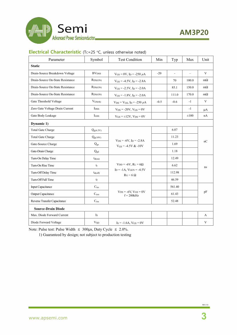
Electrical Characteristic (TC=25 °C, unless otherwise noted)
Parameter Symbol Test Condition Min Typ Max Unit Static
Drain-Source Breakdown Voltage BVDSS VGS = 0V, ID = -250 µA -20 - – V
Drain-Source On-State Resistance RDS(ON) VGS = -4.5V, ID = -2.8A 70 100.0 mΩ
Drain-Source On-State Resistance RDS(ON) VGS = -2.5V, ID = -2.0A 85.1 150.0 mΩ
Drain-Source On-State Resistance RDS(ON) VGS = -1.8V, ID = -2.0A 111.0 170.0 mΩ
Gate Threshold Voltage VGS(th) VDS = VGS, ID = -250 µA -0.5 -0.6 -1 V
Zero Gate Voltage Drain Current IDSS VDS = -20V, VGS = 0V -1 μA
Gate Body Leakage IGSS VGS = ±12V, VDS = 0V ±100 nA
Dynamic 1)
Total Gate Charge Qg(4.5V)
VDS = -6V, ID = -2.8A
VGS = -4.5V & -10V
6.07
nC Total Gate Charge Qg(10V) 11.23 Gate-Source Charge Qgs 1.69 Gate-Drain Charge Qgd 1.18 Turn-On Delay Time td(on)
VDD = -6V, RL = 6Ω
ID = -1A, VGEN = -4.5V
RG = 6 Ω
12.49
ns
Turn-On Rise Time tr 6.62 Turn-Off Delay Time td(off) 112.98 Turn-Off Fall Time tf 46.59 Input Capacitance Ciss
561.40 pF
Output Capacitance Coss 61.43 Reverse Transfer Capacitance Crss 52.48
Source-Drain Diode
Max. Diode Forward Current IS A
Diode Forward Voltage VSD IS = -1.6A, VGS = 0V V
Note: Pulse test: Pulse Width ≤ 300μs, Duty Cycle ≤ 2.0%. 1) Guaranteed by design; not subject to production testing
VDS = -6V, VGS = 0V f = 200kHz

AM3P20
REV. 01
www.apsemi.com 4
Typical Performance Characteristics
AM3P20
REV. 01
www.apsemi.com 5
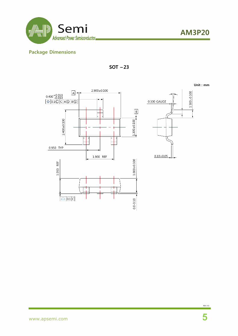
Package Dimensions
SOT -23
Unit : mm
AM3P20
REV. 01
www.apsemi.com 6
Revision History
No Date Contents
1 2015-08-30 Initial Brief Datasheet Release

AM3P20
REV. 01
www.apsemi.com 7
http://www.apsemi.com
IMPORTANT NOTICE
AP Semiconductor co, Ltd reserves the right to make changes without further notice to any products or specifications herein. AP Semiconductor co, Ltd does not assume any responsibility for use of any its products for any particular purpose, nor does AP Semiconductor co, Ltd assume any liability arising out of the application or use of any its products or circuits. AP Semiconductor co, Ltd does not convey any license under its patent rights or other rights nor the rights of others.
AP Semiconductor Co., Ltd Contact. Tel 82.70.4693.2299 FAX 82.70.4000.4009
E-mail: [email protected]
© 2015 AP semiconductor Co., Ltd. –Printed in KOREA –All Rights Reserved.