Embed Size (px)
Citation preview

AM243x Sitara™ Microcontrollers
1 FeaturesProcessor cores:• Up to 2× Dual-core Arm® Cortex®-R5F MCU
subsystems operating at up to 800 MHz, highly-integrated for real-time processing– Dual-core Arm® Cortex®-R5F clusters support
dual-core and single-core operation– 32KB ICache and 32KB DCache per R5F core
with SECDED ECC on all memories– Single-core: 128KB TCM per cluster (128KB
TCM per R5F core)– Dual-core: 128KB TCM per cluster (64KB TCM
per R5F core)• 1× Single-core Arm® Cortex®-M4F MCU at up to
400 MHz– 256KB SRAM with SECDED ECC
Memory subsystem:• Up to 2MB of On-chip RAM (OCSRAM) with
SECDED ECC:– Can be divided into smaller banks in
increments of 256KB for as many as 8 separate memory banks
– Each memory bank can be allocated to a single core to facilitate software task partitioning
• DDR Subsystem (DDRSS)– Supports LPDDR4, DDR4 memory types– 16-Bit data bus with inline ECC– Supports speeds up to 1600 MT/s
Industrial subsystem:• 2× Gigabit Industrial Communication Subsystems
(PRU_ICSSG)– Optional support for Profinet IRT, Profinet
RT, EtherNet/IP, EtherCAT, Time-Sensitive Networking (TSN), and other Networking Protocols
– Backwards compatibility with 10/100Mb PRU_ICSS
– Each PRU_ICSSG contains:• 3× PRU RISC Cores per Slice (2× Slice per
PRU_ICSSG)– PRU General Use core (PRU)– PRU Real-Time Unit core (PRU-RTU)– PRU Transmit core (PRU-TX)
• Each PRU core supports the following features:– Instruction RAM with ECC– Broadside RAM– Multiplier with optional accumulator
(MAC)
– CRC16/32 hardware accelerator– Byte swap for Big/Little Endian
conversion– SUM32 hardware accelerator for UDP
checksum– Task Manager for preemption support
• Up to 2× Ethernet ports– RGMII (10/100/1000)– MII (10/100)
• Three Data RAMs with ECC• 8 banks of 30 × 32-bit register scratchpad
memory• Interrupt controller and task manager• 2× 64-bit Industrial Ethernet Peripherals
(IEPs) for time stamping and other time synchronization functions
• 18× Sigma-Delta Filter Module (SDFM) interfaces– Short circuit logic– Over-current logic
• 6× Multi-protocol position encoder interfaces• 1× Enhanced Capture Module (ECAP)• 16550-compatible UART
– Dedicated 192-MHz clock to support 12-Mbps PROFIBUS
System on Chip (SoC) services:• Device Management Security Controller (DMSC-L)
– Centralized SoC system controller– Manages system services including initial boot,
security, and clock/reset/power management– Communication with various processing units
over message manager– Simplified interface for optimizing unused
peripherals– On-Chip Debug functionality through JTAG and
Trace interfaces)• Data Movement Subsystem (DMSS)
– Block Copy DMA (BCDMA)– Packet DMA (PKTDMA)– Secure Proxy (SEC_PROXY)– Ring Accelerator (RINGACC)
• Time Sync Subsystem– Central Platform Time Sync (CPTS) module– Timer Manager (TIMERMANAGER) with 1024
timers– Time Sync and Compare event interrupt routers
Security:• Secure Boot supported
– Hardware-enforced Root-of-Trust (RoT)– Support to switch RoT via backup key
AD
VAN
CE
INFO
RM
ATIO
N
AM2434, AM2432, AM2431SPRSP65C – APRIL 2021 – REVISED MARCH 2022
An IMPORTANT NOTICE at the end of this data sheet addresses availability, warranty, changes, use in safety-critical applications, intellectual property matters and other important disclaimers. ADVANCE INFORMATION for preproduction products; subject to change without notice.

– Support for takeover protection, IP protection, and anti-roll back protection
• Support for cryptographic acceleration– Session-aware cryptographic engine with ability
to auto-switch key-material based on incoming data stream
– Supports cryptographic cores• AES – 128/192/256 Bits key sizes• 3DES – 56/112/168 Bits key sizes• MD5, SHA1• SHA2 – 224/256/384/512• DRBG with true random number generator• PKA (Public Key Accelerator) to Assist in
RSA/ECC processing– DMA support
• Debugging security– Secure software controlled debug access– Security aware debugging
• Secure storage support• On-the-Fly encryption (OTFE) support for OSPI
interface in XIP mode• Networking security support for data (Payload)
encryption/authentication via packet based hardware cryptographic engine
• DMSC-L co-processor for key and security management, with dedicated device level interconnect
High-speed interfaces:• 1× Integrated Ethernet switch supporting up to 2
external ports (CPSW3G)– Up to 2 Ethernet ports
• RGMII (10/100/1000)• RMII (10/100)
– IEEE 1588 (2008 Annex D, Annex E, Annex F) with 802.1AS PTP
– Clause 45 MDIO PHY management– Energy efficient Ethernet (802.3az)
• 1× PCI-Express® Gen2 controller (PCIE)– Supports Gen2 operation– Supports Single Lane operation
• 1× USB 3.1-Gen1 Dual-role Device (DRD) Subsystem (USBSS)– One shared USBSS port for enhanced
SuperSpeed Gen1 or USB 2.0– Port configurable as USB host, USB peripheral,
or USB Dual-role Device– Integrated USB VBUS detection
• 1× Serializer/Deserializer (SERDES)– One SERDES lane to support either PCI-
Express® Gen2 or USB SuperSpeed Gen1
General connectivity peripherals:• 6× Inter-Integrated Circuit (I2C) ports
• 9× configurable Universal Asynchronous Receive/Transmit (UART) modules
• 1× 12-bit Analog-to-Digital Converters (ADC)– Up to 4 MSPS– 8× multiplexed analog inputs
• 7× Multichannel Serial Peripheral Interfaces (MCSPI) controllers
• 3× General-Purpose I/O (GPIO) modules
Industrial and control interfaces:• 9× Enhanced Pulse-Width Modulator (EPWM)
modules• 3× Enhanced Capture (ECAP) modules• 3× Enhanced Quadrature Encoder Pulse (EQEP)
modules• 2× Modular Controller Area Network (MCAN)
modules with full CAN-FD support• 2× Fast Serial Interface Transmitter (FSI_TX)
cores• 6× Fast Serial Interface Receiver (FSI_RX) cores
Media and data storage:• 2× MultiMedia Card/Secure Digital (MMC/SD)
interfaces– One 4-bit for SD/SDIO– One 8-bit for eMMC– Integrated analog switch for voltage switching
between 3.3V to 1.8V for high-speed cards• 1× General-Purpose Memory Controller (GPMC)
– 16-bit parallel bus with 133 MHz clock or– 32-bit parallel bus with 100 MHz clock– Error Location Module (ELM) support
• 1× Flash Subsystem (FSS) that can be configured as one Octal SPI (OSPI) flash interfaces or one Quad SPI (QSPI)
Power management:• Simplified power sequence• Dual-voltage I/O Support• Integrated SDIO LDO for handling automatic
voltage transition for SD interface• Integrated voltage supervisor for safety monitoring
of over-under voltage conditions• Integrated power supply glitch detector for
detecting fast supply transients
Functional Safety:• Functional Safety-Compliant Targeted
– Developed for functional safety applications– Documentation will be available to aid IEC
61508 functional safety system design– Systematic capability up to SIL 3– Hardware integrity up to SIL 2 targeted for MCU
domain– Quality-managed MAIN Domain
AM2434, AM2432, AM2431SPRSP65C – APRIL 2021 – REVISED MARCH 2022 www.ti.com
AD
VAN
CE IN
FOR
MATIO
N
2 Submit Document Feedback Copyright © 2022 Texas Instruments Incorporated
Product Folder Links: AM2434 AM2432 AM2431

– Safety-related certification• IEC 61508 certification planned
– ECC or parity on calculation-critical memories– ECC and parity on select internal bus
interconnects– Built-In Self-Test (BIST) for CPU and on-chip
RAM– Error Signaling Module (ESM) with external
error pin– Run-time safety diagnostics, including:
• Voltage, Temperature, and Clock Monitoring• Windowed Watchdog Timers• CRC Engine for memory integrity checks
– MCU Domain with dedicated memory, interfaces, and M4F core capable of being isolated from the larger SoC with Freedom From Interference (FFI) features• Separate interconnect• Firewalls and timeout gaskets• Dedicated PLL• Dedicated I/O supply• Separate reset
SoC architecture:• Supports primary boot from UART, I2C, OSPI/
QSPI Flash, SPI Flash, parallel NOR Flash, parallel NAND Flash, SD, eMMC, USB 2.0, PCIe, and Ethernet interfaces
• 16-nm FinFET technology
Package options:• ALV - 17.2 mm × 17.2 mm, 0.8-mm pitch (441-pin)
FCBGA [Lidded] Flip-Chip Ball Grid Array package• ALX - 11.0 mm × 11.0 mm, 0.5-mm pitch (293-
pin) FC/CSP [SiP] Flip-Chip/Chip Scale Package package
2 Applications• Programmable Logic Controller (PLC)• Motor Drives• Remote I/O• Industrial Robots
3 DescriptionAM243x is an extension of Sitara’s industrial-grade portfolio into high-performance microcontrollers. The AM243x device is built for industrial applications, such as motor drives and remote I/O modules, which require a combination of real-time communications and processing. The AM243x family provides scalable performance with up to four Cortex-R5F MCUs, one Cortex-M4F, and two instances of Sitara’s gigabit TSN-enabled PRU-ICSSG.
The AM243x SoC architecture was designed to provide best-in-class real-time performance through the high-performance Arm Cortex-R5F cores, Tightly-Coupled Memory banks, configurable SRAM partitioning, and dedicated low-latency paths to and from peripherals for rapid data movement in and out of the SoC. This deterministic architecture allows for AM243x to handle the tight control loops found in servo drives while the peripherals like FSI, GPMC, ECAPs, PWMs, and encoder interfaces help enable a number of different architectures found in these systems.
The SoC provides flexible industrial communications capability including full protocol stacks for EtherCAT slave, PROFINET device, EtherNet/IP adapter, and IO-Link Master. The PRU-ICSSG further provides capability for gigabit and TSN based protocols. In addition, the PRU-ICSSG also enables additional interfaces in the SoC including a UART interface, sigma delta decimation filters, and absolute encoder interfaces.
Functional safety features can be enabled through the integrated Cortex-M4F along with its dedicated peripherals which can all be isolated from the rest of the SoC. AM243x also supports secure boot.
www.ti.comAM2434, AM2432, AM2431
SPRSP65C – APRIL 2021 – REVISED MARCH 2022
AD
VAN
CE
INFO
RM
ATIO
N
Copyright © 2022 Texas Instruments Incorporated Submit Document Feedback 3
Product Folder Links: AM2434 AM2432 AM2431

Device InformationPART NUMBER PACKAGE(1) BODY SIZE
XAM2434...ALV(2) (441-Pin) FCBGA [Lidded] 17.2 mm × 17.2 mm
XAM2434...ALX(2) (293-Pin) FC/CSP [SiP] 11.0 mm × 11.0 mm
XAM2432...ALV(2) (441-Pin) FCBGA [Lidded] 17.2 mm × 17.2 mm
XAM2432...ALX(2) (293-Pin) FC/CSP [SiP] 11.0 mm × 11.0 mm
XAM2431..ALV(2) (441-Pin) FCBGA [Lidded] 17.2 mm × 17.2 mm
XAM2431..ALX(2) (293-Pin) FC/CSP [SiP] 11.0 mm × 11.0 mm
(1) For more information, see Section 11, Mechanical, Packaging, and Orderable Information.(2) All XAM243x part numbers correspond to the fully featured XAM2434ASFGGAALX or
XAM2434ASFGGAALV.
AM2434, AM2432, AM2431SPRSP65C – APRIL 2021 – REVISED MARCH 2022 www.ti.com
AD
VAN
CE IN
FOR
MATIO
N
4 Submit Document Feedback Copyright © 2022 Texas Instruments Incorporated
Product Folder Links: AM2434 AM2432 AM2431

3.1 Functional Block DiagramFigure 3-1 is the functional block diagram for the device.
Industrial Connectivity
PRU-ICSS(Gb)
System Memory
Security
A 243xM
intro_001
2 MB SRAM with ECC DDR4/LPDDR4 with inline ECC 2x MMCSD
AESMD5
SHA
3DES
PKA DRBGSecureBoot
System Services
12x GP Timers 4x WWDTSync
Manager
3x EQEP
3x ECAP
9x EPWM 4x I2C
GPIO
5x MCSPI
1x ADC
7x UART
PCIe1x Single lane
Gen 2
GPMC / ELM
8x FSI
OSPI or QSPI
2x CAN-FD
2x GMACEncoder
with 9x ∆∑
PRU-ICSS(Gb)
2x GMACEncoder
with 9x ∆∑
1x USB 3.1 DRD
2-port GbEthernet
General Connectivity
2x I2C
GPIO
2x MCSPI
2x UART
Isolated Connectivity(A)
(for use with Cortex-M4F)
128KB TCM
Arm®
Cortex -R5F®
128KB TCM
Arm®
Cortex -R5F®
Arm®
Cortex -R5F®
Arm®
Cortex -R5F®
Arm®
®Cortex -M4F
256KB SRAM
Real-time cores Isolated core(A)
A. Isolation of peripherals and M4F core is an optional feature. MCU domain resources are shared across SoC when in non-isolated configuration.
B. USB3.1 and PCIe share a common SerDes lane.
Figure 3-1. Functional Block Diagram
www.ti.comAM2434, AM2432, AM2431
SPRSP65C – APRIL 2021 – REVISED MARCH 2022
AD
VAN
CE
INFO
RM
ATIO
N
Copyright © 2022 Texas Instruments Incorporated Submit Document Feedback 5
Product Folder Links: AM2434 AM2432 AM2431

Table of Contents1 Features............................................................................12 Applications..................................................................... 33 Description.......................................................................3
3.1 Functional Block Diagram........................................... 54 Revision History.............................................................. 75 Device Comparison......................................................... 8
5.1 Related Products...................................................... 106 Terminal Configuration and Functions........................11
6.1 Pin Diagram.............................................................. 116.2 Pin Attributes.............................................................136.3 Signal Descriptions................................................... 576.4 Pin Connectivity Requirements.................................94
7 Specifications................................................................ 997.1 Absolute Maximum Ratings...................................... 997.2 ESD Ratings........................................................... 1017.3 Power-On Hours (POH).......................................... 1017.4 Recommended Operating Conditions.....................1027.5 Operating Performance Points................................1047.6 Power Consumption Summary............................... 1047.7 Electrical Characteristics.........................................1057.8 VPP Specifications for One-Time Programmable
(OTP) eFuses............................................................ 111
7.9 Thermal Resistance Characteristics....................... 1127.10 Timing and Switching Characteristics................... 114
8 Detailed Description....................................................2088.1 Overview................................................................. 2088.2 Processor Subsystems........................................... 2098.3 Accelerators and Coprocessors..............................2108.4 Other Subsystems.................................................. 210
9 Applications, Implementation, and Layout............... 2189.1 Device Connection and Layout Fundamentals....... 2199.2 Peripheral- and Interface-Specific Design
Information................................................................ 22010 Device and Documentation Support........................226
10.1 Device Nomenclature............................................22610.2 Tools and Software............................................... 22810.3 Documentation Support........................................ 22910.4 Support Resources............................................... 22910.5 Trademarks...........................................................22910.6 Electrostatic Discharge Caution............................23010.7 Glossary................................................................230
11 Mechanical, Packaging, and Orderable Information.................................................................. 23111.1 Packaging Information.......................................... 231
AM2434, AM2432, AM2431SPRSP65C – APRIL 2021 – REVISED MARCH 2022 www.ti.com
AD
VAN
CE IN
FOR
MATIO
N
6 Submit Document Feedback Copyright © 2022 Texas Instruments Incorporated
Product Folder Links: AM2434 AM2432 AM2431

4 Revision History
Changes from July 16, 2021 to March 14, 2022 (from Revision B (July 2021) to Revision C (March 2022)) Page• (Features): Deleted Trusted Execution Environment (TEE). Arm TrustZone® support for Cortex-A cores only
bullets. Not supported on AM243x devices........................................................................................................ 1• (Device Information): Added footnote for AM2432_ALV/ALX and AM2431_ALV/ALX device options regarding
pre-production part numbers.............................................................................................................................. 3• (Device Comparison): Clarified speed grade options for each device. Also clarified functional safety support
and added a note that references the Nomenclature Description table..............................................................8• (AM243x_ALX Package - Unsupported Interfaces and Signals): Updated table and associated notes...........58• (Pin Connectivity Requirements [was "Connections for Unused Pins"]): Added new pin connection
requirements and updated SERDES power pin connection requirements to include a condition of device boundary scan usage....................................................................................................................................... 94
• (Pin Connectivity Requirements): Included VMON connectivity requirements................................................. 94• (Absolute Maximum Ratings): Replaced free-air in the table description with junction and moved MCU_PORz
from a row of dual-voltage fail-safe pins to its own row.................................................................................... 99• (Recommended Operating Conditions): Replaced free-air in the table description with junction and added a
note to VDD_MMC0 and VDD_DLL_MMC0...................................................................................................102• (Recommended Operating Conditions): Combined VDDS_DDR and VDDS_DDR_C into a single row and
added a note that explains these two power rails should be powered from the same source........................102• Updated the "The voltage at the device ball must never ..." footnote............................................................. 102• (Speed Grade Maximum Frequency): Added Speed Grade K - ICSSG operating frequency (250 MHz)...... 104• (Speed Grade Maximum Frequency): Updated Note 1 to reference the AM64x\AM243x DDR Board Design
and Layout Guidelines.................................................................................................................................... 104• (Fail-Safe Reset Electrical Characteristics): Updated values for VILSS and VIHSS parameters.......................105• (LVCMOS Electrical Characteristics): Corrected the VOH MIN value for 1.8V Mode...................................... 109• (Recommended Operating Conditions for OTP eFuse Programming): Replaced free-air in the table
description with junction and changed operating temperature description to remove ambient and replace with junction. Also removed the recommendation for using a specific power management solution..................... 111
• (ALV Package Thermal Resistance Characteristics): Updated TBD values in the table with actual values... 112• (ALX Package Thermal Resistance Characteristics): Updated TBD values in the table with actual values...112• (System Timing): Removed the maximum input slew rate requirement from the Systems Timing Conditions
table................................................................................................................................................................ 118• (Clock Timing): Added MCU_EXT_REFCLK0 to the Clock Timing Requirements, and added
MCU_SYSCLKOUT0 and MCU_OBSCLK0 to the Clock Switching Characteristics......................................123• (MCU_OSC0 Internal Oscillator Clock Source): Added a note to define the maximum ESRxtal value based on
the Cshunt parameter....................................................................................................................................... 125• (MCU_OSC0 Start-up Time): Updated signal names in figure....................................................................... 125• (CPSW3G): Added IOSET information...........................................................................................................131• (DDRSS Switching Characteristics): Added a note that clarifies the min cycle time definition and references
the AM64x\AM243x DDR Board Design and Layout Guidelines.................................................................... 136• (GPMC): Added IOSET information................................................................................................................143• (GPMC and NOR Flash — Synchronous Mode): Added a note to Timing Requirements and Switching
Characteristics tables to clarify maximum frequency relationship to data bus width...................................... 143• (System Power Supply Monitor Design Guidelines): Updated maximum and minumum threshold values to
remove a few mV of rounding error in example provided............................................................................... 224• (Standard Package Symbolization): Updated package symbolization figure................................................. 227• (Device Naming Convention): Added K option to Device Speed Grades row to table. Added Q1 Automotive
Designator Row to table................................................................................................................................. 227• (Tools and Software): Updated the supported development tools.................................................................. 228• (Documentation Support) Updated/Changed the URL of the Silicon Errata reference...................................229
www.ti.comAM2434, AM2432, AM2431
SPRSP65C – APRIL 2021 – REVISED MARCH 2022
AD
VAN
CE
INFO
RM
ATIO
N
Copyright © 2022 Texas Instruments Incorporated Submit Document Feedback 7
Product Folder Links: AM2434 AM2432 AM2431

5 Device ComparisonTable 5-1 shows a comparison between devices, highlighting the differences.
NoteAvailability of features listed in this table are a function of shared IO pins, where IO signals associated with many of the features are multiplexed to a limited number of pins. The SysConfig tool should be used to assign signal functions to pins. This will provide a better understanding of limitations associated with pin multiplexing.
NoteTo understand what device features are currently supported by TI Software Development Kits (SDKs), see the AM243x SW Build Sheet.
Table 5-1. Device ComparisonFEATURES(1) REFERENCE
NAMEAM2434
(ALV)AM2432
(ALV)AM2431
(ALV)AM2434
(ALX)AM2432
(ALX)AM2431
(ALX)
JTAG DEVICE ID COMPARISON (FEATURES)
CTRLMMR_JTAG_DEVICE_ID[31:13] DEVICE_ID register bit-field value(2)
C: -----------D: 0x19064E: 0x19065F: 0x19066
C: 0x19023D: 0x19024E: 0x19025F: 0x19026
C: 0x19003D: 0x19004E: -----------F: -----------
C: -----------D: 0x19064E: 0x19065F: 0x19066
C: 0x19023D: 0x19024E: 0x19025F: 0x19026
C: 0x19003D: 0x19004E: -----------F: -----------
PROCESSORS AND ACCELERATORSSpeed Grades (See Table 7-1) S S S,K S S S,K
Arm Cortex-R5F Processor R5FSS 2 × Dual Core
2 × Single Core
1 × Single Core
2 × Dual Core
2× Single Core
1 × Single Core
Arm Cortex-M4F Processor M4FSSSingle Core
Functional Safety Optional(3)
Single Core
Device Management Security Controller DMSC-L Yes Yes
Crypto Accelerators Security Yes Yes
PROGRAM AND DATA STORAGEShared On-Chip Memory (OCSRAM) in MAIN Domain OCSRAM 2MB 2MB
R5F Tightly Coupled Memory (TCM)(4) TCM 256KB 256KB 128KB 256KB 256KB 128KB
Shared On-Chip Memory (OCSRAM) in MCU Domain MCU_MSRAM 256KB 256KB
DDR4/LPDDR4 DDR Subsystem DDRSS Up to 2GB (16-bit data) with inline ECC -
General-Purpose Memory Controller w/Error Location Module (ELM) GPMC w/ELM Up to 1GB with ECC -
PERIPHERALSModular Controller Area Network Interface MCAN 2 2
Full CAN-FD Support(5) MCAN Optional Optional
General-Purpose I/O GPIO Up to 198 Up to 148
Inter-Integrated Circuit Interface I2C 6 (2 in MCU Domain) 3 (MAIN Domain Only)
Analog-to-Digital Converter ADC 12-bit 10-bit
Multichannel Serial Peripheral Interface MCSPI 7 (2 in MCU Domain) 4 (MAIN Domain Only)
MultiMedia Card/ Secure Digital Interface
MMC0 eMMC (8-bits) -
MMC1 SD/SDIO (4-bits) SD/SDIO (4-bits)
AM2434, AM2432, AM2431SPRSP65C – APRIL 2021 – REVISED MARCH 2022 www.ti.com
AD
VAN
CE IN
FOR
MATIO
N
8 Submit Document Feedback Copyright © 2022 Texas Instruments Incorporated
Product Folder Links: AM2434 AM2432 AM2431

Table 5-1. Device Comparison (continued)FEATURES(1) REFERENCE
NAMEAM2434
(ALV)AM2432
(ALV)AM2431
(ALV)AM2434
(ALX)AM2432
(ALX)AM2431
(ALX)
Fast Serial InterfaceFSI_TX 2 1
FSI_RX 6 4
Flash Subsystem (FSS) OSPI/QSPI Yes(6) QSPI-Mode Only
PCI Express Port with Integrated PHY PCIE Single Lane -
Programmable Real-Time Unit Subsystem(7)
(PRU Cores, eGPIO, UART, ECAP. EPWM)
PRU_ICSSG 2 2
Industrial Communication Subsystem Support(8)
(RGMII/MII and additional Networking Interfaces)
PRU_ICSSG Optional Optional
Gigabit Ethernet Interface CPSW3G Yes (2 External Ports) Yes (2 External Ports)
General-Purpose Timers TIMER 16 (4 in MCU Domain) 16 (4 in MCU Domain)
Enhanced Pulse-Width Modulation Module EPWM 9 7(9)
Enhanced Capture Module ECAP 3 3
Enhanced Quadrature Encoder Pulse Module EQEP 3 3
Universal Asynchronous Receiver/Transmitter UART 9 (2 in MCU Domain) 8 (1 in MCU Domain)
Universal Serial Bus (USB3.1 Gen1) SuperSpeed Dual-Role-Device (DRD) Port with SS PHY
USB Yes No USB SuperSpeed Support(USB2 Only)
(1) Features noted as “not supported” or "-", must not be used. Their functionality is not supported by TI for this family of devices. These features are subject to removal without notice on future device revisions. Any information regarding the unsupported features has been retained in the documentation solely for the purpose of clarifying signal names or for consistency with previous feature descriptions.
(2) For more details about the CTRLMMR_JTAG_DEVICE_ID register and DEVICE_ID bit field, see the device's associated Technical Reference Manual.
(3) Functional Safety is available when selecting an orderable part number that includes a feature code of F. Refer to Table 10-1 for definition of feature codes.
(4) The R5F cores share Tightly Coupled Memory within a cluster and can be allocated per system requirements.(5) Full CAN-FD Support is available when selecting an orderable part number that includes a feature code of E or F. Refer to Table 10-1
for definition of feature codes.(6) One simultaneous flash interface configured as OSPI0 or QSPI0.(7) Programmable Real-Time Unit Subsystem is available when selecting an orderable part number that includes a feature code of C.
Refer to Table 10-1 for definition of feature codes.(8) Industrial Communication Subsystem support is available when selecting an orderable part number that includes a feature code of D,
E, or F. Refer to Table 10-1 for definition of feature codes.(9) Only the A output signal is available for the EHRPWM5 instance of the ALX package type.
www.ti.comAM2434, AM2432, AM2431
SPRSP65C – APRIL 2021 – REVISED MARCH 2022
AD
VAN
CE
INFO
RM
ATIO
N
Copyright © 2022 Texas Instruments Incorporated Submit Document Feedback 9
Product Folder Links: AM2434 AM2432 AM2431

5.1 Related ProductsSitara™ processors Broad family of scalable processors based on Arm® Cortex® cores with flexible accelerators, peripherals, connectivity and unified software support – perfect for sensors to servers. Sitara processors have the reliability needed for use in industrial applications.
AM243x Sitara™ microcontrollers AM243x microcontrollers enable gigabit industrial Ethernet networks, robust operation with extensive ECC on memories, and enhanced security features.
Sitara™ processors - Applications Sitara™ processors provide scalable solutions for a wide range of applications from HMIs and gateways to more complex equipment such as drives and substation automation equipment. Sitara processors also offer multi-protocol support for industrial communication protocols such as EtherCAT®, Ethernet/IP, and Profinet.
Sitara™ processors - Reference designs TI provides many reference designs containing ‘building block’ solutions to enable customers to rapidly develop their own unique products and solutions.
Companion Products for AM243x Review products that are frequently purchased or used in conjunction with this product to complete your design.
AM2434, AM2432, AM2431SPRSP65C – APRIL 2021 – REVISED MARCH 2022 www.ti.com
AD
VAN
CE IN
FOR
MATIO
N
10 Submit Document Feedback Copyright © 2022 Texas Instruments Incorporated
Product Folder Links: AM2434 AM2432 AM2431

6 Terminal Configuration and Functions6.1 Pin Diagram
Note
The terms "ball", "pin", and "terminal" are used interchangeably throughout the document. An attempt is made to use "ball" only when referring to the physical package.
The diagrams in this section are used in conjunction with the other Terminal Configuration and Functions tables to locate signal names and ball grid numbers.
6.1.1 AM243x ALV Pin Diagram
ALV FCBGA-N441 Pin Diagram shows the ball locations for the lidded 441-ball flip chip ball grid array (FCBGA) package.
Figure 6-1. ALV FCBGA-N441 Pin Diagram (Bottom View)
www.ti.comAM2434, AM2432, AM2431
SPRSP65C – APRIL 2021 – REVISED MARCH 2022
AD
VAN
CE
INFO
RM
ATIO
N
Copyright © 2022 Texas Instruments Incorporated Submit Document Feedback 11
Product Folder Links: AM2434 AM2432 AM2431

6.1.2 AM243x ALX Pin Diagram
ALX FCBGA-N293 Pin Diagram shows the ball locations for the non-lidded 293-ball flip chip ball grid array (FCBGA) package.
Figure 6-2. ALX FCBGA-N293 Pin Diagram (Bottom View)
AM2434, AM2432, AM2431SPRSP65C – APRIL 2021 – REVISED MARCH 2022 www.ti.com
AD
VAN
CE IN
FOR
MATIO
N
12 Submit Document Feedback Copyright © 2022 Texas Instruments Incorporated
Product Folder Links: AM2434 AM2432 AM2431

6.2 Pin AttributesThe following list describes the contents of each column in the Pin Attributes table:
1. BALL NUMBER: Ball numbers assigned to each terminal of the Ball Grid Array package.2. BALL NAME: Ball name assigned to each terminal of the Ball Grid Array package (this name is typically
taken from the primary MUXMODE 0 signal function).3. SIGNAL NAME: Signal name(s) of all dedicated and pin multiplexed signal functions associated with a ball.
Note
The Pin Attributes table, defines the SoC pin multiplexed signal function implemented at the pin and does not define secondary multiplexing of signal functions implemented in device subsystems. Secondary multiplexing of signal functions are not described in this table. For more information on secondary multiplexed signal functions, see the respective peripheral chapter of the device TRM.
4. MUX MODE: The MUXMODE value associated with each pin multiplexed signal function:• MUXMODE 0 is the primary pin multiplexed signal function. However, the primary pin multiplexed signal
function is not necessarily the default pin multiplexed signal function.• MUXMODE values 1 through 15 are possible for pin multiplexed signal functions. However, not all
MUXMODE values have been implemented. The only valid MUXMODE values are those defined as pin multiplexed signal functions within the Pin Attributes table. Only valid values of MUXMODE should be used.
• Bootstrap defines SOC configuration pins, where the logic state applied to each pin is latched on the rising edge of PORz_OUT. These input signal functions are fixed to their respective pins and are not programmable via MUXMODE.
• An empty box or "-" means Not Applicable.
Note• The value found in the MUX MODE AFTER RESET column defines the default pin multiplexed
signal function selected when MCU_PORz is deasserted.• Configuring two pins to the same pin multiplexed signal function can yield unexpected results
and is not supported. This can be prevented with proper software configuration.• Configuring a pad to an undefined multiplexing mode will result in undefined behavior and
should be avoided.
5. TYPE: Signal type and direction:Signal Type Description
I Input
O Output
IO Input, Output, or simultaneously Input and Output
IOD Input, Output, or simultaneously Input and Output, with open-drain output function
IOZ Input, Output, or simultaneously Input and Output, with three-state output function
OZ Output with three-state output function
A Analog
PWR Power
GND Ground
CAP LDO Capacitor
www.ti.comAM2434, AM2432, AM2431
SPRSP65C – APRIL 2021 – REVISED MARCH 2022
AD
VAN
CE
INFO
RM
ATIO
N
Copyright © 2022 Texas Instruments Incorporated Submit Document Feedback 13
Product Folder Links: AM2434 AM2432 AM2431

6. DSIS: The deselected input state (DSIS) indicates the state driven to the subsystem input (logic "0", logic "1", or "pad" level) when the pin multiplexed signal function is not selected by MUXMODE.• 0: Logic 0 driven to the subsystem input.• 1: Logic 1 driven to the subsystem input.• pad: Logic state of the pad is driven to the subsystem input.• An empty box or "-" means Not Applicable.
7. BALL STATE DURING RESET (RX/TX/PULL): State of the terminal while MCU_PORz is asserted, where RX defines the state of the input buffer, TX defines the state of the output buffer, and PULL defines the state of internal pull resistors:• RX (Input buffer)
– Off: The input buffer is disabled.– On: The input buffer is enabled.
• TX (Output buffer)– Off: The output buffer is disabled.– Low: The output buffer is enabled and drives VOL.
• PULL (Internal pull resistors)– Off: Internal pull resistors are turned off.– Up: Internal pull-up resistor is turned on.– Down: Internal pull-down resistor is turned on.
• An empty box or "-" means Not Applicable.
8. BALL STATE AFTER RESET (RX/TX/PULL): State of the terminal after MCU_PORz is deasserted, where RX defines the state of the input buffer, TX defines the state of the output buffer, and PULL defines the state of internal pull resistors:• RX (Input buffer)
– Off: The input buffer is disabled.– On: The input buffer is enabled.
• TX (Output buffer)– Off: The output buffer is disabled.– SS: The subsystem selected with MUXMODE determines the output buffer state.
• PULL (Internal pull resistors)– Off: Internal pull resistors are turned off.– Up: Internal pull-up resistor is turned on.– Down: Internal pull-down resistor is turned on.
• An empty box or "-" means Not Applicable.
9. MUX MODE AFTER RESET: The value found in this column defines the default pin multiplexed signal function after MCU_PORz is deasserted.• An empty box means Not Applicable.
10. I/O VOLTAGE VALUE: This column describes I/O operating voltage options of the respective power supply, when applicable.• An empty box or "-" means Not Applicable.
For more information, see valid operating voltage range(s) defined for each power supply in Recommended Operating Conditions.
11. POWER: The power supply of the associated I/O, when applicable.• An empty box or "-" means Not Applicable.
12. HYS: Indicates if the input buffer associated with this I/O has hysteresis:• Yes: Hysteresis Support• No: No Hysteresis Support• An empty box or "-" means Not Applicable.
For more information, see the hysteresis values in Electrical Characteristics.
AM2434, AM2432, AM2431SPRSP65C – APRIL 2021 – REVISED MARCH 2022 www.ti.com
AD
VAN
CE IN
FOR
MATIO
N
14 Submit Document Feedback Copyright © 2022 Texas Instruments Incorporated
Product Folder Links: AM2434 AM2432 AM2431

13. BUFFER TYPE: This column defines the buffer type associated with a terminal. This information can be used to determine the applicable Electrical Characteristics table.• An empty box or "-" means Not Applicable.
For electrical characteristics, refer to the appropriate buffer type table in Electrical Characteristics.
14. PULL UP/DOWN TYPE: Indicates the presence of an internal pull-up or pull-down resistor. Internal resistors can be enabled or disabled via software.• PU: Internal pull-up Only• PD: Internal pull-down Only• PU/PD: Internal pull-up and pull-down• An empty box or "-" means No internal pull.
15. Pad Configuration Register Name: This is the name of the device pad/pin configuration register.16. Pad Configuration Register Address: This is the memory address of the device pad/pin configuration
register.
www.ti.comAM2434, AM2432, AM2431
SPRSP65C – APRIL 2021 – REVISED MARCH 2022
AD
VAN
CE
INFO
RM
ATIO
N
Copyright © 2022 Texas Instruments Incorporated Submit Document Feedback 15
Product Folder Links: AM2434 AM2432 AM2431

Table 6-1. Pin Attributes (ALV, ALX Packages)ALV
BALLNUMBER
[1]
ALX BALL
NUMBER [1]
BALL NAME [2]/PADCONFIG
REGISTER [15]/PADCONFIG
ADDRESS [16]
SIGNAL NAME [3]MUX
MODE [4]
TYPE [5]
DSIS [6]
BALLSTATE
DURINGRESET [7]
BALLSTATEAFTER
RESET [8]
MUXMODEAFTER
RESET [9]
IOVOLTAGE
[10]POWER [11] HYS
[12]BUFFER
TYPE [13]
PULLTYPE [14]
G20 H21 ADC0_AIN0 ADC0_AIN0 A 1.8 V VDDA_ADC0 Yes ADC12B
F20 F19 ADC0_AIN1 ADC0_AIN1 A 1.8 V VDDA_ADC0 Yes ADC12B
E21 F21 ADC0_AIN2 ADC0_AIN2 A 1.8 V VDDA_ADC0 Yes ADC12B
D20 F20 ADC0_AIN3 ADC0_AIN3 A 1.8 V VDDA_ADC0 Yes ADC12B
G21 H20 ADC0_AIN4 ADC0_AIN4 A 1.8 V VDDA_ADC0 Yes ADC12B
F21 E21 ADC0_AIN5 ADC0_AIN5 A 1.8 V VDDA_ADC0 Yes ADC12B
F19 G20 ADC0_AIN6 ADC0_AIN6 A 1.8 V VDDA_ADC0 Yes ADC12B
E20 E20 ADC0_AIN7 ADC0_AIN7 A 1.8 V VDDA_ADC0 Yes ADC12B
H12 D12 CAP_VDDS0 CAP_VDDS0 CAP
T7 N5 CAP_VDDS1 CAP_VDDS1 CAP
R11 U9 CAP_VDDS2 CAP_VDDS2 CAP
N14 R16 CAP_VDDS3 CAP_VDDS3 CAP
M16 N18 CAP_VDDS4 CAP_VDDS4 CAP
L13 M18 CAP_VDDS5 CAP_VDDS5 CAP
K15 J17 CAP_VDDSHV_MMC1 CAP_VDDSHV_MMC1 CAP
H10 D9 CAP_VDDS_MCU CAP_VDDS_MCU CAP
H2 DDR0_ACT_n DDR0_ACT_n O 1.1 V/1.2 V VDDS_DDR, VDDS_DDR_C
DDR
H1 DDR0_ALERT_n DDR0_ALERT_n IO 1.1 V/1.2 V VDDS_DDR, VDDS_DDR_C
DDR
J5 DDR0_CAS_n DDR0_CAS_n O 1.1 V/1.2 V VDDS_DDR, VDDS_DDR_C
DDR
K5 DDR0_PAR DDR0_PAR O 1.1 V/1.2 V VDDS_DDR, VDDS_DDR_C
DDR
F6 DDR0_RAS_n DDR0_RAS_n O 1.1 V/1.2 V VDDS_DDR, VDDS_DDR_C
DDR
H4 DDR0_WE_n DDR0_WE_n O 1.1 V/1.2 V VDDS_DDR, VDDS_DDR_C
DDR
D2 DDR0_A0 DDR0_A0 O 1.1 V/1.2 V VDDS_DDR, VDDS_DDR_C
DDR
C5 DDR0_A1 DDR0_A1 O 1.1 V/1.2 V VDDS_DDR, VDDS_DDR_C
DDR
E2 DDR0_A2 DDR0_A2 O 1.1 V/1.2 V VDDS_DDR, VDDS_DDR_C
DDR
D4 DDR0_A3 DDR0_A3 O 1.1 V/1.2 V VDDS_DDR, VDDS_DDR_C
DDR
D3 DDR0_A4 DDR0_A4 O 1.1 V/1.2 V VDDS_DDR, VDDS_DDR_C
DDR
F2 DDR0_A5 DDR0_A5 O 1.1 V/1.2 V VDDS_DDR, VDDS_DDR_C
DDR
AM2434, AM2432, AM2431SPRSP65C – APRIL 2021 – REVISED MARCH 2022 www.ti.com
AD
VAN
CE IN
FOR
MATIO
N
16 Submit Document Feedback Copyright © 2022 Texas Instruments Incorporated
Product Folder Links: AM2434 AM2432 AM2431

Table 6-1. Pin Attributes (ALV, ALX Packages) (continued)ALV
BALLNUMBER
[1]
ALX BALL
NUMBER [1]
BALL NAME [2]/PADCONFIG
REGISTER [15]/PADCONFIG
ADDRESS [16]
SIGNAL NAME [3]MUX
MODE [4]
TYPE [5]
DSIS [6]
BALLSTATE
DURINGRESET [7]
BALLSTATEAFTER
RESET [8]
MUXMODEAFTER
RESET [9]
IOVOLTAGE
[10]POWER [11] HYS
[12]BUFFER
TYPE [13]
PULLTYPE [14]
J2 DDR0_A6 DDR0_A6 O 1.1 V/1.2 V VDDS_DDR, VDDS_DDR_C
DDR
L5 DDR0_A7 DDR0_A7 O 1.1 V/1.2 V VDDS_DDR, VDDS_DDR_C
DDR
J3 DDR0_A8 DDR0_A8 O 1.1 V/1.2 V VDDS_DDR, VDDS_DDR_C
DDR
J4 DDR0_A9 DDR0_A9 O 1.1 V/1.2 V VDDS_DDR, VDDS_DDR_C
DDR
K3 DDR0_A10 DDR0_A10 O 1.1 V/1.2 V VDDS_DDR, VDDS_DDR_C
DDR
J1 DDR0_A11 DDR0_A11 O 1.1 V/1.2 V VDDS_DDR, VDDS_DDR_C
DDR
M5 DDR0_A12 DDR0_A12 O 1.1 V/1.2 V VDDS_DDR, VDDS_DDR_C
DDR
K4 DDR0_A13 DDR0_A13 O 1.1 V/1.2 V VDDS_DDR, VDDS_DDR_C
DDR
G4 DDR0_BA0 DDR0_BA0 O 1.1 V/1.2 V VDDS_DDR, VDDS_DDR_C
DDR
G5 DDR0_BA1 DDR0_BA1 O 1.1 V/1.2 V VDDS_DDR, VDDS_DDR_C
DDR
G2 DDR0_BG0 DDR0_BG0 O 1.1 V/1.2 V VDDS_DDR, VDDS_DDR_C
DDR
H3 DDR0_BG1 DDR0_BG1 O 1.1 V/1.2 V VDDS_DDR, VDDS_DDR_C
DDR
H5 DDR0_CAL0 DDR0_CAL0 A 1.1 V/1.2 V VDDS_DDR, VDDS_DDR_C
DDR
F1 DDR0_CK0 DDR0_CK0 O 1.1 V/1.2 V VDDS_DDR, VDDS_DDR_C
DDR
E1 DDR0_CK0_n DDR0_CK0_n O 1.1 V/1.2 V VDDS_DDR, VDDS_DDR_C
DDR
F4 DDR0_CKE0 DDR0_CKE0 O 1.1 V/1.2 V VDDS_DDR, VDDS_DDR_C
DDR
F3 DDR0_CKE1 DDR0_CKE1 O 1.1 V/1.2 V VDDS_DDR, VDDS_DDR_C
DDR
E3 DDR0_CS0_n DDR0_CS0_n O 1.1 V/1.2 V VDDS_DDR, VDDS_DDR_C
DDR
E4 DDR0_CS1_n DDR0_CS1_n O 1.1 V/1.2 V VDDS_DDR, VDDS_DDR_C
DDR
B2 DDR0_DM0 DDR0_DM0 IO 1.1 V/1.2 V VDDS_DDR, VDDS_DDR_C
DDR
M2 DDR0_DM1 DDR0_DM1 IO 1.1 V/1.2 V VDDS_DDR, VDDS_DDR_C
DDR
A3 DDR0_DQ0 DDR0_DQ0 IO 1.1 V/1.2 V VDDS_DDR, VDDS_DDR_C
DDR
A2 DDR0_DQ1 DDR0_DQ1 IO 1.1 V/1.2 V VDDS_DDR, VDDS_DDR_C
DDR
www.ti.comAM2434, AM2432, AM2431
SPRSP65C – APRIL 2021 – REVISED MARCH 2022
AD
VAN
CE
INFO
RM
ATIO
N
Copyright © 2022 Texas Instruments Incorporated Submit Document Feedback 17
Product Folder Links: AM2434 AM2432 AM2431

Table 6-1. Pin Attributes (ALV, ALX Packages) (continued)ALV
BALLNUMBER
[1]
ALX BALL
NUMBER [1]
BALL NAME [2]/PADCONFIG
REGISTER [15]/PADCONFIG
ADDRESS [16]
SIGNAL NAME [3]MUX
MODE [4]
TYPE [5]
DSIS [6]
BALLSTATE
DURINGRESET [7]
BALLSTATEAFTER
RESET [8]
MUXMODEAFTER
RESET [9]
IOVOLTAGE
[10]POWER [11] HYS
[12]BUFFER
TYPE [13]
PULLTYPE [14]
B5 DDR0_DQ2 DDR0_DQ2 IO 1.1 V/1.2 V VDDS_DDR, VDDS_DDR_C
DDR
A4 DDR0_DQ3 DDR0_DQ3 IO 1.1 V/1.2 V VDDS_DDR, VDDS_DDR_C
DDR
B3 DDR0_DQ4 DDR0_DQ4 IO 1.1 V/1.2 V VDDS_DDR, VDDS_DDR_C
DDR
C4 DDR0_DQ5 DDR0_DQ5 IO 1.1 V/1.2 V VDDS_DDR, VDDS_DDR_C
DDR
C2 DDR0_DQ6 DDR0_DQ6 IO 1.1 V/1.2 V VDDS_DDR, VDDS_DDR_C
DDR
B4 DDR0_DQ7 DDR0_DQ7 IO 1.1 V/1.2 V VDDS_DDR, VDDS_DDR_C
DDR
N5 DDR0_DQ8 DDR0_DQ8 IO 1.1 V/1.2 V VDDS_DDR, VDDS_DDR_C
DDR
L4 DDR0_DQ9 DDR0_DQ9 IO 1.1 V/1.2 V VDDS_DDR, VDDS_DDR_C
DDR
L2 DDR0_DQ10 DDR0_DQ10 IO 1.1 V/1.2 V VDDS_DDR, VDDS_DDR_C
DDR
M3 DDR0_DQ11 DDR0_DQ11 IO 1.1 V/1.2 V VDDS_DDR, VDDS_DDR_C
DDR
N4 DDR0_DQ12 DDR0_DQ12 IO 1.1 V/1.2 V VDDS_DDR, VDDS_DDR_C
DDR
N3 DDR0_DQ13 DDR0_DQ13 IO 1.1 V/1.2 V VDDS_DDR, VDDS_DDR_C
DDR
M4 DDR0_DQ14 DDR0_DQ14 IO 1.1 V/1.2 V VDDS_DDR, VDDS_DDR_C
DDR
N2 DDR0_DQ15 DDR0_DQ15 IO 1.1 V/1.2 V VDDS_DDR, VDDS_DDR_C
DDR
C1 DDR0_DQS0 DDR0_DQS0 IO 1.1 V/1.2 V VDDS_DDR, VDDS_DDR_C
DDR
B1 DDR0_DQS0_n DDR0_DQS0_n IO 1.1 V/1.2 V VDDS_DDR, VDDS_DDR_C
DDR
N1 DDR0_DQS1 DDR0_DQS1 IO 1.1 V/1.2 V VDDS_DDR, VDDS_DDR_C
DDR
M1 DDR0_DQS1_n DDR0_DQS1_n IO 1.1 V/1.2 V VDDS_DDR, VDDS_DDR_C
DDR
E5 DDR0_ODT0 DDR0_ODT0 O 1.1 V/1.2 V VDDS_DDR, VDDS_DDR_C
DDR
F5 DDR0_ODT1 DDR0_ODT1 O 1.1 V/1.2 V VDDS_DDR, VDDS_DDR_C
DDR
D5 DDR0_RESET0_n DDR0_RESET0_n O 1.1 V/1.2 V VDDS_DDR, VDDS_DDR_C
DDR
AM2434, AM2432, AM2431SPRSP65C – APRIL 2021 – REVISED MARCH 2022 www.ti.com
AD
VAN
CE IN
FOR
MATIO
N
18 Submit Document Feedback Copyright © 2022 Texas Instruments Incorporated
Product Folder Links: AM2434 AM2432 AM2431

Table 6-1. Pin Attributes (ALV, ALX Packages) (continued)ALV
BALLNUMBER
[1]
ALX BALL
NUMBER [1]
BALL NAME [2]/PADCONFIG
REGISTER [15]/PADCONFIG
ADDRESS [16]
SIGNAL NAME [3]MUX
MODE [4]
TYPE [5]
DSIS [6]
BALLSTATE
DURINGRESET [7]
BALLSTATEAFTER
RESET [8]
MUXMODEAFTER
RESET [9]
IOVOLTAGE
[10]POWER [11] HYS
[12]BUFFER
TYPE [13]
PULLTYPE [14]
D18 ECAP0_IN_APWM_OUT
PADCONFIG1560x000F4270
ECAP0_IN_APWM_OUT 0 IO 0 Off / Off / Off Off / Off / Off 7 1.8 V/3.3 V VDDSHV0 Yes LVCMOS PU/PD
SYNC0_OUT 1 O
CPTS0_RFT_CLK 2 I 0
CP_GEMAC_CPTS0_RFT_CLK 5 I 0
SPI4_CS3 6 IO 1
GPIO1_68 7 IO pad
D10 C5 EMU0
MCU_PADCONFIG310x0408407C
EMU0 0 IO On / Off / Up On / Off / Up 0 1.8 V/3.3 V VDDSHV_MCU Yes LVCMOS PU/PD
E10 B3 EMU1
MCU_PADCONFIG320x04084080
EMU1 0 IO On / Off / Up On / Off / Up 0 1.8 V/3.3 V VDDSHV_MCU Yes LVCMOS PU/PD
MCU_OBSCLK0 15 O
C19 EXTINTn
PADCONFIG1580x000F4278
EXTINTn 0 I 1 Off / Off / Off Off / Off / Off 7 1.8 V/3.3 V VDDSHV0 Yes I2C OD FS
GPIO1_70 7 IO pad
A19 A18 EXT_REFCLK1
PADCONFIG1570x000F4274
EXT_REFCLK1 0 I 0 Off / Off / Off Off / Off / Off 7 1.8 V/3.3 V VDDSHV0 Yes LVCMOS PU/PD
SYNC1_OUT 1 O
SPI2_CS3 2 IO 1
CLKOUT0 5 O
GPIO1_69 7 IO pad
P16 GPMC0_ADVn_ALE
PADCONFIG330x000F4084
GPMC0_ADVn_ALE 0 O Off / Off / Off Off / Off / Off 7 1.8 V/3.3 V VDDSHV3 Yes LVCMOS PU/PD
FSI_RX5_CLK 1 I 0
UART5_RXD 2 I 1
EHRPWM_TZn_IN3 3 I 0
TRC_DATA15 6 O
GPIO0_32 7 IO pad
PRG0_PWM3_TZ_IN 9 I 0
R17 GPMC0_CLK
PADCONFIG310x000F407C
GPMC0_CLK 0 O 0 Off / Off / Off Off / Off / Off 7 1.8 V/3.3 V VDDSHV3 Yes LVCMOS PU/PD
FSI_RX4_CLK 1 I 0
UART4_RTSn 2 O
EHRPWM3_SYNCO 3 O
GPMC0_FCLK_MUX 4 O
TRC_DATA14 6 O
GPIO0_31 7 IO pad
PRG0_PWM3_TZ_OUT 9 O
www.ti.comAM2434, AM2432, AM2431
SPRSP65C – APRIL 2021 – REVISED MARCH 2022
AD
VAN
CE
INFO
RM
ATIO
N
Copyright © 2022 Texas Instruments Incorporated Submit Document Feedback 19
Product Folder Links: AM2434 AM2432 AM2431

Table 6-1. Pin Attributes (ALV, ALX Packages) (continued)ALV
BALLNUMBER
[1]
ALX BALL
NUMBER [1]
BALL NAME [2]/PADCONFIG
REGISTER [15]/PADCONFIG
ADDRESS [16]
SIGNAL NAME [3]MUX
MODE [4]
TYPE [5]
DSIS [6]
BALLSTATE
DURINGRESET [7]
BALLSTATEAFTER
RESET [8]
MUXMODEAFTER
RESET [9]
IOVOLTAGE
[10]POWER [11] HYS
[12]BUFFER
TYPE [13]
PULLTYPE [14]
N17 GPMC0_DIR
PADCONFIG410x000F40A4
GPMC0_DIR 0 O Off / Off / Off Off / Off / Off 7 1.8 V/3.3 V VDDSHV3 Yes LVCMOS PU/PD
EQEP0_B 3 I 0
GPIO0_40 7 IO pad
EHRPWM6_B 8 IO 0
PRG1_PWM2_B0 9 IO 1
R18 GPMC0_OEn_REn
PADCONFIG340x000F4088
GPMC0_OEn_REn 0 O Off / Off / Off Off / Off / Off 7 1.8 V/3.3 V VDDSHV3 Yes LVCMOS PU/PD
FSI_RX5_D0 1 I 0
UART5_TXD 2 O
EHRPWM4_A 3 IO 0
TRC_DATA16 6 O
GPIO0_33 7 IO pad
PRG0_PWM3_A1 9 IO 0
T21 GPMC0_WEn
PADCONFIG350x000F408C
GPMC0_WEn 0 O Off / Off / Off Off / Off / Off 7 1.8 V/3.3 V VDDSHV3 Yes LVCMOS PU/PD
FSI_RX5_D1 1 I 0
UART5_RTSn 2 O
EHRPWM4_B 3 IO 0
TRC_DATA17 6 O
GPIO0_34 7 IO pad
PRG0_PWM3_B1 9 IO 1
N16 GPMC0_WPn
PADCONFIG400x000F40A0
GPMC0_WPn 0 O Off / Off / Off Off / Off / Off 7 1.8 V/3.3 V VDDSHV3 Yes LVCMOS PU/PD
FSI_TX1_CLK 1 O
EQEP0_A 3 I 0
GPMC0_A22 4 OZ
TRC_DATA22 6 O
GPIO0_39 7 IO pad
EHRPWM6_A 8 IO 0
PRG1_PWM2_A0 9 IO 0
T20 R21 GPMC0_AD0
PADCONFIG150x000F403C
GPMC0_AD0 0 IO 0 On / Off / Off On / Off / Off 7 1.8 V/3.3 V VDDSHV3 Yes LVCMOS PU/PD
FSI_RX2_CLK 1 I 0
UART2_RXD 2 I 1
EHRPWM0_SYNCI 3 I 0
TRC_CLK 6 O
GPIO0_15 7 IO pad
BOOTMODE00 Bootstrap
I
AM2434, AM2432, AM2431SPRSP65C – APRIL 2021 – REVISED MARCH 2022 www.ti.com
AD
VAN
CE IN
FOR
MATIO
N
20 Submit Document Feedback Copyright © 2022 Texas Instruments Incorporated
Product Folder Links: AM2434 AM2432 AM2431

Table 6-1. Pin Attributes (ALV, ALX Packages) (continued)ALV
BALLNUMBER
[1]
ALX BALL
NUMBER [1]
BALL NAME [2]/PADCONFIG
REGISTER [15]/PADCONFIG
ADDRESS [16]
SIGNAL NAME [3]MUX
MODE [4]
TYPE [5]
DSIS [6]
BALLSTATE
DURINGRESET [7]
BALLSTATEAFTER
RESET [8]
MUXMODEAFTER
RESET [9]
IOVOLTAGE
[10]POWER [11] HYS
[12]BUFFER
TYPE [13]
PULLTYPE [14]
U21 R20 GPMC0_AD1
PADCONFIG160x000F4040
GPMC0_AD1 0 IO 0 On / Off / Off On / Off / Off 7 1.8 V/3.3 V VDDSHV3 Yes LVCMOS PU/PD
FSI_RX2_D0 1 I 0
UART2_TXD 2 O
EHRPWM0_SYNCO 3 O
TRC_CTL 6 O
GPIO0_16 7 IO pad
PRG0_PWM2_TZ_OUT 9 O
BOOTMODE01 Bootstrap
I
T18 T19 GPMC0_AD2
PADCONFIG170x000F4044
GPMC0_AD2 0 IO 0 On / Off / Off On / Off / Off 7 1.8 V/3.3 V VDDSHV3 Yes LVCMOS PU/PD
FSI_RX2_D1 1 I 0
UART2_RTSn 2 O
EHRPWM_TZn_IN0 3 I 0
TRC_DATA0 6 O
GPIO0_17 7 IO pad
PRG0_PWM2_TZ_IN 9 I 0
BOOTMODE02 Bootstrap
I
U20 V21 GPMC0_AD3
PADCONFIG180x000F4048
GPMC0_AD3 0 IO 0 On / Off / Off On / Off / Off 7 1.8 V/3.3 V VDDSHV3 Yes LVCMOS PU/PD
FSI_RX3_CLK 1 I 0
UART3_RXD 2 I 1
EHRPWM0_A 3 IO 0
TRC_DATA1 6 O
GPIO0_18 7 IO pad
PRG0_PWM2_A0 9 IO 0
BOOTMODE03 Bootstrap
I
U18 U21 GPMC0_AD4
PADCONFIG190x000F404C
GPMC0_AD4 0 IO 0 On / Off / Off On / Off / Off 7 1.8 V/3.3 V VDDSHV3 Yes LVCMOS PU/PD
FSI_RX3_D0 1 I 0
UART3_TXD 2 O
EHRPWM0_B 3 IO 0
TRC_DATA2 6 O
GPIO0_82 7 IO pad
PRG0_PWM2_B0 9 IO 1
BOOTMODE04 Bootstrap
I
www.ti.comAM2434, AM2432, AM2431
SPRSP65C – APRIL 2021 – REVISED MARCH 2022
AD
VAN
CE
INFO
RM
ATIO
N
Copyright © 2022 Texas Instruments Incorporated Submit Document Feedback 21
Product Folder Links: AM2434 AM2432 AM2431

Table 6-1. Pin Attributes (ALV, ALX Packages) (continued)ALV
BALLNUMBER
[1]
ALX BALL
NUMBER [1]
BALL NAME [2]/PADCONFIG
REGISTER [15]/PADCONFIG
ADDRESS [16]
SIGNAL NAME [3]MUX
MODE [4]
TYPE [5]
DSIS [6]
BALLSTATE
DURINGRESET [7]
BALLSTATEAFTER
RESET [8]
MUXMODEAFTER
RESET [9]
IOVOLTAGE
[10]POWER [11] HYS
[12]BUFFER
TYPE [13]
PULLTYPE [14]
U19 T20 GPMC0_AD5
PADCONFIG200x000F4050
GPMC0_AD5 0 IO 0 On / Off / Off On / Off / Off 7 1.8 V/3.3 V VDDSHV3 Yes LVCMOS PU/PD
FSI_RX3_D1 1 I 0
UART3_RTSn 2 O
EHRPWM1_A 3 IO 0
TRC_DATA3 6 O
GPIO0_83 7 IO pad
PRG0_PWM2_A1 9 IO 0
BOOTMODE05 Bootstrap
I
V20 T18 GPMC0_AD6
PADCONFIG210x000F4054
GPMC0_AD6 0 IO 0 On / Off / Off On / Off / Off 7 1.8 V/3.3 V VDDSHV3 Yes LVCMOS PU/PD
FSI_RX4_D0 1 I 0
UART4_RXD 2 I 1
EHRPWM1_B 3 IO 0
TRC_DATA4 6 O
GPIO0_21 7 IO pad
PRG0_PWM2_B1 9 IO 1
BOOTMODE06 Bootstrap
I
V21 U19 GPMC0_AD7
PADCONFIG220x000F4058
GPMC0_AD7 0 IO 0 On / Off / Off On / Off / Off 7 1.8 V/3.3 V VDDSHV3 Yes LVCMOS PU/PD
FSI_RX4_D1 1 I 0
UART4_TXD 2 O
EHRPWM_TZn_IN1 3 I 0
EHRPWM8_A 4 IO 0
TRC_DATA5 6 O
GPIO0_22 7 IO pad
PRG1_PWM2_A2 9 IO 0
BOOTMODE07 Bootstrap
I
V19 U18 GPMC0_AD8
PADCONFIG230x000F405C
GPMC0_AD8 0 IO 0 On / Off / Off On / Off / Off 7 1.8 V/3.3 V VDDSHV3 Yes LVCMOS PU/PD
FSI_RX0_CLK 1 I 0
UART2_CTSn 2 I 1
EHRPWM2_A 3 IO 0
TRC_DATA6 6 O
GPIO0_23 7 IO pad
PRG0_PWM2_A2 9 IO 0
BOOTMODE08 Bootstrap
I
AM2434, AM2432, AM2431SPRSP65C – APRIL 2021 – REVISED MARCH 2022 www.ti.com
AD
VAN
CE IN
FOR
MATIO
N
22 Submit Document Feedback Copyright © 2022 Texas Instruments Incorporated
Product Folder Links: AM2434 AM2432 AM2431

Table 6-1. Pin Attributes (ALV, ALX Packages) (continued)ALV
BALLNUMBER
[1]
ALX BALL
NUMBER [1]
BALL NAME [2]/PADCONFIG
REGISTER [15]/PADCONFIG
ADDRESS [16]
SIGNAL NAME [3]MUX
MODE [4]
TYPE [5]
DSIS [6]
BALLSTATE
DURINGRESET [7]
BALLSTATEAFTER
RESET [8]
MUXMODEAFTER
RESET [9]
IOVOLTAGE
[10]POWER [11] HYS
[12]BUFFER
TYPE [13]
PULLTYPE [14]
T17 U20 GPMC0_AD9
PADCONFIG240x000F4060
GPMC0_AD9 0 IO 0 On / Off / Off On / Off / Off 7 1.8 V/3.3 V VDDSHV3 Yes LVCMOS PU/PD
FSI_RX0_D0 1 I 0
UART3_CTSn 2 I 1
EHRPWM2_B 3 IO 0
TRC_DATA7 6 O
GPIO0_24 7 IO pad
PRG0_PWM2_B2 9 IO 1
BOOTMODE09 Bootstrap
I
R16 V20 GPMC0_AD10
PADCONFIG250x000F4064
GPMC0_AD10 0 IO 0 On / Off / Off On / Off / Off 7 1.8 V/3.3 V VDDSHV3 Yes LVCMOS PU/PD
FSI_RX0_D1 1 I 0
UART4_CTSn 2 I 1
EHRPWM_TZn_IN2 3 I 0
EHRPWM8_B 4 IO 0
TRC_DATA8 6 O
GPIO0_25 7 IO pad
PRG1_PWM2_B2 9 IO 1
BOOTMODE10 Bootstrap
I
W20 W20 GPMC0_AD11
PADCONFIG260x000F4068
GPMC0_AD11 0 IO 0 On / Off / Off On / Off / Off 7 1.8 V/3.3 V VDDSHV3 Yes LVCMOS PU/PD
FSI_RX1_CLK 1 I 0
UART5_CTSn 2 I 1
EQEP1_A 3 I 0
TRC_DATA9 6 O
GPIO0_26 7 IO pad
EHRPWM7_A 8 IO 0
BOOTMODE11 Bootstrap
I
W21 Y20 GPMC0_AD12
PADCONFIG270x000F406C
GPMC0_AD12 0 IO 0 On / Off / Off On / Off / Off 7 1.8 V/3.3 V VDDSHV3 Yes LVCMOS PU/PD
FSI_RX1_D0 1 I 0
UART6_CTSn 2 I 1
EQEP1_B 3 I 0
TRC_DATA10 6 O
GPIO0_27 7 IO pad
EHRPWM7_B 8 IO 0
BOOTMODE12 Bootstrap
I
www.ti.comAM2434, AM2432, AM2431
SPRSP65C – APRIL 2021 – REVISED MARCH 2022
AD
VAN
CE
INFO
RM
ATIO
N
Copyright © 2022 Texas Instruments Incorporated Submit Document Feedback 23
Product Folder Links: AM2434 AM2432 AM2431

Table 6-1. Pin Attributes (ALV, ALX Packages) (continued)ALV
BALLNUMBER
[1]
ALX BALL
NUMBER [1]
BALL NAME [2]/PADCONFIG
REGISTER [15]/PADCONFIG
ADDRESS [16]
SIGNAL NAME [3]MUX
MODE [4]
TYPE [5]
DSIS [6]
BALLSTATE
DURINGRESET [7]
BALLSTATEAFTER
RESET [8]
MUXMODEAFTER
RESET [9]
IOVOLTAGE
[10]POWER [11] HYS
[12]BUFFER
TYPE [13]
PULLTYPE [14]
V18 Y19 GPMC0_AD13
PADCONFIG280x000F4070
GPMC0_AD13 0 IO 0 On / Off / Off On / Off / Off 7 1.8 V/3.3 V VDDSHV3 Yes LVCMOS PU/PD
FSI_RX1_D1 1 I 0
EHRPWM3_A 3 IO 0
TRC_DATA11 6 O
GPIO0_28 7 IO pad
PRG0_PWM3_A0 9 IO 0
BOOTMODE13 Bootstrap
I
Y21 Y18 GPMC0_AD14
PADCONFIG290x000F4074
GPMC0_AD14 0 IO 0 On / Off / Off On / Off / Off 7 1.8 V/3.3 V VDDSHV3 Yes LVCMOS PU/PD
FSI_TX0_D0 1 O
UART6_RXD 2 I 1
EHRPWM3_B 3 IO 0
TRC_DATA12 6 O
GPIO0_29 7 IO pad
PRG0_PWM3_B0 9 IO 1
BOOTMODE14 Bootstrap
I
Y20 AA19 GPMC0_AD15
PADCONFIG300x000F4078
GPMC0_AD15 0 IO 0 On / Off / Off On / Off / Off 7 1.8 V/3.3 V VDDSHV3 Yes LVCMOS PU/PD
FSI_TX0_D1 1 O
UART6_TXD 2 O
EHRPWM3_SYNCI 3 I 0
TRC_DATA13 6 O
GPIO0_30 7 IO pad
BOOTMODE15 Bootstrap
I
P17 GPMC0_BE0n_CLE
PADCONFIG360x000F4090
GPMC0_BE0n_CLE 0 O Off / Off / Off Off / Off / Off 7 1.8 V/3.3 V VDDSHV3 Yes LVCMOS PU/PD
FSI_TX1_D0 1 O
UART6_RTSn 2 O
EHRPWM_TZn_IN4 3 I 0
EHRPWM7_A 5 IO 0
TRC_DATA18 6 O
GPIO0_35 7 IO pad
PRG1_PWM2_A1 9 IO 0
AM2434, AM2432, AM2431SPRSP65C – APRIL 2021 – REVISED MARCH 2022 www.ti.com
AD
VAN
CE IN
FOR
MATIO
N
24 Submit Document Feedback Copyright © 2022 Texas Instruments Incorporated
Product Folder Links: AM2434 AM2432 AM2431

Table 6-1. Pin Attributes (ALV, ALX Packages) (continued)ALV
BALLNUMBER
[1]
ALX BALL
NUMBER [1]
BALL NAME [2]/PADCONFIG
REGISTER [15]/PADCONFIG
ADDRESS [16]
SIGNAL NAME [3]MUX
MODE [4]
TYPE [5]
DSIS [6]
BALLSTATE
DURINGRESET [7]
BALLSTATEAFTER
RESET [8]
MUXMODEAFTER
RESET [9]
IOVOLTAGE
[10]POWER [11] HYS
[12]BUFFER
TYPE [13]
PULLTYPE [14]
T19 P21 GPMC0_BE1n
PADCONFIG370x000F4094
GPMC0_BE1n 0 O Off / Off / Off Off / Off / Off 7 1.8 V/3.3 V VDDSHV3 Yes LVCMOS PU/PD
FSI_TX0_CLK 1 O
EHRPWM5_A 3 IO 0
TRC_DATA19 6 O
GPIO0_36 7 IO pad
PRG0_PWM3_A2 9 IO 0
R19 GPMC0_CSn0
PADCONFIG420x000F40A8
GPMC0_CSn0 0 O Off / Off / Off Off / Off / Off 7 1.8 V/3.3 V VDDSHV3 Yes LVCMOS PU/PD
EQEP0_S 3 IO 0
TRC_DATA23 6 O
GPIO0_41 7 IO pad
EHRPWM6_SYNCI 8 I 0
R20 GPMC0_CSn1
PADCONFIG430x000F40AC
GPMC0_CSn1 0 O Off / Off / Off Off / Off / Off 7 1.8 V/3.3 V VDDSHV3 Yes LVCMOS PU/PD
EQEP0_I 3 IO 0
EHRPWM_TZn_IN2 5 I 0
GPIO0_42 7 IO pad
EHRPWM6_SYNCO 8 O
PRG1_PWM2_TZ_OUT 9 O
P19 GPMC0_CSn2
PADCONFIG440x000F40B0
GPMC0_CSn2 0 O Off / Off / Off Off / Off / Off 7 1.8 V/3.3 V VDDSHV3 Yes LVCMOS PU/PD
I2C2_SCL 1 IOD 1
TIMER_IO8 2 IO 0
EQEP1_S 3 IO 0
EHRPWM_TZn_IN4 5 I 0
GPIO0_43 7 IO pad
PRG1_PWM2_TZ_IN 9 I 0
R21 GPMC0_CSn3
PADCONFIG450x000F40B4
GPMC0_CSn3 0 O Off / Off / Off Off / Off / Off 7 1.8 V/3.3 V VDDSHV3 Yes LVCMOS PU/PD
I2C2_SDA 1 IOD 1
TIMER_IO9 2 IO 0
EQEP1_I 3 IO 0
GPMC0_A20 4 OZ
EHRPWM_TZn_IN5 5 I 0
GPIO0_44 7 IO pad
W19 GPMC0_WAIT0
PADCONFIG380x000F4098
GPMC0_WAIT0 0 I 1 Off / Off / Off Off / Off / Off 7 1.8 V/3.3 V VDDSHV3 Yes LVCMOS PU/PD
EHRPWM5_B 3 IO 0
TRC_DATA20 6 O
GPIO0_37 7 IO pad
PRG0_PWM3_B2 9 IO 1
www.ti.comAM2434, AM2432, AM2431
SPRSP65C – APRIL 2021 – REVISED MARCH 2022
AD
VAN
CE
INFO
RM
ATIO
N
Copyright © 2022 Texas Instruments Incorporated Submit Document Feedback 25
Product Folder Links: AM2434 AM2432 AM2431

Table 6-1. Pin Attributes (ALV, ALX Packages) (continued)ALV
BALLNUMBER
[1]
ALX BALL
NUMBER [1]
BALL NAME [2]/PADCONFIG
REGISTER [15]/PADCONFIG
ADDRESS [16]
SIGNAL NAME [3]MUX
MODE [4]
TYPE [5]
DSIS [6]
BALLSTATE
DURINGRESET [7]
BALLSTATEAFTER
RESET [8]
MUXMODEAFTER
RESET [9]
IOVOLTAGE
[10]POWER [11] HYS
[12]BUFFER
TYPE [13]
PULLTYPE [14]
Y18 GPMC0_WAIT1
PADCONFIG390x000F409C
GPMC0_WAIT1 0 I 1 Off / Off / Off Off / Off / Off 7 1.8 V/3.3 V VDDSHV3 Yes LVCMOS PU/PD
FSI_TX1_D1 1 O
EHRPWM_TZn_IN5 3 I 0
GPMC0_A21 4 OZ
EHRPWM7_B 5 IO 0
TRC_DATA21 6 O
GPIO0_38 7 IO pad
PRG1_PWM2_B1 9 IO 1
A18 B16 I2C0_SCL
PADCONFIG1520x000F4260
I2C0_SCL 0 IOD 1 Off / Off / Off On / SS / Off 7 1.8 V/3.3 V VDDSHV0 Yes I2C OD FS
UART6_CTSn 4 I 1
GPIO1_64 7 IO pad
B18 B15 I2C0_SDA
PADCONFIG1530x000F4264
I2C0_SDA 0 IOD 1 Off / Off / Off On / SS / Off 7 1.8 V/3.3 V VDDSHV0 Yes I2C OD FS
UART6_RTSn 4 O
GPIO1_65 7 IO pad
C18 A17 I2C1_SCL
PADCONFIG1540x000F4268
I2C1_SCL 0 IOD 1 Off / Off / Off Off / Off / Off 7 1.8 V/3.3 V VDDSHV0 Yes LVCMOS PU/PD
CPTS0_HW1TSPUSH 1 I 0
TIMER_IO0 2 IO 0
SPI2_CS1 3 IO 1
GPIO1_66 7 IO pad
B19 B18 I2C1_SDA
PADCONFIG1550x000F426C
I2C1_SDA 0 IOD 1 Off / Off / Off Off / Off / Off 7 1.8 V/3.3 V VDDSHV0 Yes LVCMOS PU/PD
CPTS0_HW2TSPUSH 1 I 0
TIMER_IO1 2 IO 0
SPI2_CS2 3 IO 1
GPIO1_67 7 IO pad
B17 A14 MCAN0_RX
PADCONFIG1490x000F4254
MCAN0_RX 0 I 1 Off / Off / Off Off / Off / Off 7 1.8 V/3.3 V VDDSHV0 Yes LVCMOS PU/PD
UART4_TXD 1 O
TIMER_IO3 2 IO 0
SYNC3_OUT 3 O
SPI4_CS2 6 IO 1
GPIO1_61 7 IO pad
EQEP2_S 8 IO 0
UART0_RIn 9 I 1
AM2434, AM2432, AM2431SPRSP65C – APRIL 2021 – REVISED MARCH 2022 www.ti.com
AD
VAN
CE IN
FOR
MATIO
N
26 Submit Document Feedback Copyright © 2022 Texas Instruments Incorporated
Product Folder Links: AM2434 AM2432 AM2431

Table 6-1. Pin Attributes (ALV, ALX Packages) (continued)ALV
BALLNUMBER
[1]
ALX BALL
NUMBER [1]
BALL NAME [2]/PADCONFIG
REGISTER [15]/PADCONFIG
ADDRESS [16]
SIGNAL NAME [3]MUX
MODE [4]
TYPE [5]
DSIS [6]
BALLSTATE
DURINGRESET [7]
BALLSTATEAFTER
RESET [8]
MUXMODEAFTER
RESET [9]
IOVOLTAGE
[10]POWER [11] HYS
[12]BUFFER
TYPE [13]
PULLTYPE [14]
A17 B13 MCAN0_TX
PADCONFIG1480x000F4250
MCAN0_TX 0 O Off / Off / Off Off / Off / Off 7 1.8 V/3.3 V VDDSHV0 Yes LVCMOS PU/PD
UART4_RXD 1 I 1
TIMER_IO2 2 IO 0
SYNC2_OUT 3 O
SPI4_CS1 6 IO 1
GPIO1_60 7 IO pad
EQEP2_I 8 IO 0
UART0_DTRn 9 O
D17 A15 MCAN1_RX
PADCONFIG1510x000F425C
MCAN1_RX 0 I 1 Off / Off / Off Off / Off / Off 7 1.8 V/3.3 V VDDSHV0 Yes LVCMOS PU/PD
I2C3_SDA 1 IOD 1
ECAP2_IN_APWM_OUT 2 IO 0
OBSCLK0 3 O
TIMER_IO5 4 IO 0
UART5_TXD 5 O
EHRPWM_SOCB 6 O
GPIO1_63 7 IO pad
EQEP2_B 8 I 0
UART0_DSRn 9 I 1
OBSCLK0 15 O
C17 B14 MCAN1_TX
PADCONFIG1500x000F4258
MCAN1_TX 0 O Off / Off / Off Off / Off / Off 7 1.8 V/3.3 V VDDSHV0 Yes LVCMOS PU/PD
I2C3_SCL 1 IOD 1
ECAP1_IN_APWM_OUT 2 IO 0
SYSCLKOUT0 3 O
TIMER_IO4 4 IO 0
UART5_RXD 5 I 1
EHRPWM_SOCA 6 O
GPIO1_62 7 IO pad
EQEP2_A 8 I 0
UART0_DCDn 9 I 1
E9 MCU_I2C0_SCL
MCU_PADCONFIG180x04084048
MCU_I2C0_SCL 0 IOD 1 Off / Off / Off On / SS / Off 7 1.8 V/3.3 V VDDSHV_MCU Yes I2C OD FS
MCU_GPIO0_18 7 IO pad
A10 MCU_I2C0_SDA
MCU_PADCONFIG190x0408404C
MCU_I2C0_SDA 0 IOD 1 Off / Off / Off On / SS / Off 7 1.8 V/3.3 V VDDSHV_MCU Yes I2C OD FS
MCU_GPIO0_19 7 IO pad
A11 MCU_I2C1_SCL
MCU_PADCONFIG200x04084050
MCU_I2C1_SCL 0 IOD 1 Off / Off / Off Off / Off / Off 7 1.8 V/3.3 V VDDSHV_MCU Yes LVCMOS PU/PD
MCU_GPIO0_20 7 IO pad
www.ti.comAM2434, AM2432, AM2431
SPRSP65C – APRIL 2021 – REVISED MARCH 2022
AD
VAN
CE
INFO
RM
ATIO
N
Copyright © 2022 Texas Instruments Incorporated Submit Document Feedback 27
Product Folder Links: AM2434 AM2432 AM2431

Table 6-1. Pin Attributes (ALV, ALX Packages) (continued)ALV
BALLNUMBER
[1]
ALX BALL
NUMBER [1]
BALL NAME [2]/PADCONFIG
REGISTER [15]/PADCONFIG
ADDRESS [16]
SIGNAL NAME [3]MUX
MODE [4]
TYPE [5]
DSIS [6]
BALLSTATE
DURINGRESET [7]
BALLSTATEAFTER
RESET [8]
MUXMODEAFTER
RESET [9]
IOVOLTAGE
[10]POWER [11] HYS
[12]BUFFER
TYPE [13]
PULLTYPE [14]
B10 MCU_I2C1_SDA
MCU_PADCONFIG210x04084054
MCU_I2C1_SDA 0 IOD 1 Off / Off / Off Off / Off / Off 7 1.8 V/3.3 V VDDSHV_MCU Yes LVCMOS PU/PD
MCU_GPIO0_21 7 IO pad
C21 D20 MCU_OSC0_XI MCU_OSC0_XI I 1.8 V VDDS_OSC Yes HFOSC
B20 C21 MCU_OSC0_XO MCU_OSC0_XO O 1.8 V VDDS_OSC Yes HFOSC
B21 C20 MCU_PORz
MCU_PADCONFIG230x0408405C
MCU_PORz 0 I 0 1.8 V VDDS_OSC Yes FS RESET
B13 A6 MCU_RESETSTATz
MCU_PADCONFIG240x04084060
MCU_RESETSTATz 0 O Off / Low / Off Off / SS / Off 0 1.8 V/3.3 V VDDSHV_MCU Yes LVCMOS PU/PD
MCU_GPIO0_22 7 IO pad
B12 A5 MCU_RESETz
MCU_PADCONFIG220x04084058
MCU_RESETz 0 I On / Off / Up On / Off / Up 0 1.8 V/3.3 V VDDSHV_MCU Yes LVCMOS PU/PD
A20 B20 MCU_SAFETY_ERRORn
MCU_PADCONFIG250x04084064
MCU_SAFETY_ERRORn 0 IO Off / Off / Down On / SS / Down 0 1.8 V VDDS_OSC Yes LVCMOS PU/PD
E6 MCU_SPI0_CLK
MCU_PADCONFIG20x04084008
MCU_SPI0_CLK 0 IO 0 Off / Off / Off Off / Off / Off 7 1.8 V/3.3 V VDDSHV_MCU Yes LVCMOS PU/PD
MCU_GPIO0_11 7 IO pad
D7 MCU_SPI1_CLK
MCU_PADCONFIG70x0408401C
MCU_SPI1_CLK 0 IO 0 Off / Off / Off Off / Off / Off 7 1.8 V/3.3 V VDDSHV_MCU Yes LVCMOS PU/PD
MCU_GPIO0_7 7 IO pad
D6 MCU_SPI0_CS0
MCU_PADCONFIG00x04084000
MCU_SPI0_CS0 0 IO 1 Off / Off / Off Off / Off / Off 7 1.8 V/3.3 V VDDSHV_MCU Yes LVCMOS PU/PD
MCU_GPIO0_13 7 IO pad
C6 MCU_SPI0_CS1
MCU_PADCONFIG10x04084004
MCU_SPI0_CS1 0 IO 1 Off / Off / Off Off / Off / Off 7 1.8 V/3.3 V VDDSHV_MCU Yes LVCMOS PU/PD
MCU_OBSCLK0 1 O
MCU_SYSCLKOUT0 2 O
MCU_GPIO0_12 7 IO pad
E7 MCU_SPI0_D0
MCU_PADCONFIG30x0408400C
MCU_SPI0_D0 0 IO 0 Off / Off / Off Off / Off / Off 7 1.8 V/3.3 V VDDSHV_MCU Yes LVCMOS PU/PD
MCU_GPIO0_10 7 IO pad
B6 MCU_SPI0_D1
MCU_PADCONFIG40x04084010
MCU_SPI0_D1 0 IO 0 Off / Off / Off Off / Off / Off 7 1.8 V/3.3 V VDDSHV_MCU Yes LVCMOS PU/PD
MCU_GPIO0_4 7 IO pad
A7 MCU_SPI1_CS0
MCU_PADCONFIG50x04084014
MCU_SPI1_CS0 0 IO 1 Off / Off / Off Off / Off / Off 7 1.8 V/3.3 V VDDSHV_MCU Yes LVCMOS PU/PD
MCU_GPIO0_5 7 IO pad
B7 MCU_SPI1_CS1
MCU_PADCONFIG60x04084018
MCU_SPI1_CS1 0 IO 1 Off / Off / Off Off / Off / Off 7 1.8 V/3.3 V VDDSHV_MCU Yes LVCMOS PU/PD
MCU_EXT_REFCLK0 1 I 0
MCU_GPIO0_6 7 IO pad
AM2434, AM2432, AM2431SPRSP65C – APRIL 2021 – REVISED MARCH 2022 www.ti.com
AD
VAN
CE IN
FOR
MATIO
N
28 Submit Document Feedback Copyright © 2022 Texas Instruments Incorporated
Product Folder Links: AM2434 AM2432 AM2431

Table 6-1. Pin Attributes (ALV, ALX Packages) (continued)ALV
BALLNUMBER
[1]
ALX BALL
NUMBER [1]
BALL NAME [2]/PADCONFIG
REGISTER [15]/PADCONFIG
ADDRESS [16]
SIGNAL NAME [3]MUX
MODE [4]
TYPE [5]
DSIS [6]
BALLSTATE
DURINGRESET [7]
BALLSTATEAFTER
RESET [8]
MUXMODEAFTER
RESET [9]
IOVOLTAGE
[10]POWER [11] HYS
[12]BUFFER
TYPE [13]
PULLTYPE [14]
C7 MCU_SPI1_D0
MCU_PADCONFIG80x04084020
MCU_SPI1_D0 0 IO 0 Off / Off / Off Off / Off / Off 7 1.8 V/3.3 V VDDSHV_MCU Yes LVCMOS PU/PD
MCU_GPIO0_8 7 IO pad
C8 MCU_SPI1_D1
MCU_PADCONFIG90x04084024
MCU_SPI1_D1 0 IO 0 Off / Off / Off Off / Off / Off 7 1.8 V/3.3 V VDDSHV_MCU Yes LVCMOS PU/PD
MCU_GPIO0_9 7 IO pad
D8 D4 MCU_UART0_CTSn
MCU_PADCONFIG120x04084030
MCU_UART0_CTSn 0 I 1 Off / Off / Off Off / Off / Off 7 1.8 V/3.3 V VDDSHV_MCU Yes LVCMOS PU/PD
MCU_TIMER_IO0 1 IO 0
MCU_SPI0_CS2 2 IO 1
MCU_GPIO0_1 7 IO pad
E8 C2 MCU_UART0_RTSn
MCU_PADCONFIG130x04084034
MCU_UART0_RTSn 0 O Off / Off / Off Off / Off / Off 7 1.8 V/3.3 V VDDSHV_MCU Yes LVCMOS PU/PD
MCU_TIMER_IO1 1 IO 0
MCU_SPI1_CS2 2 IO 1
MCU_GPIO0_0 7 IO pad
A9 D6 MCU_UART0_RXD
MCU_PADCONFIG100x04084028
MCU_UART0_RXD 0 I 1 Off / Off / Off Off / Off / Off 7 1.8 V/3.3 V VDDSHV_MCU Yes LVCMOS PU/PD
MCU_GPIO0_3 7 IO pad
A8 B2 MCU_UART0_TXD
MCU_PADCONFIG110x0408402C
MCU_UART0_TXD 0 O Off / Off / Off Off / Off / Off 7 1.8 V/3.3 V VDDSHV_MCU Yes LVCMOS PU/PD
MCU_GPIO0_2 7 IO pad
B8 MCU_UART1_CTSn
MCU_PADCONFIG160x04084040
MCU_UART1_CTSn 0 I 1 Off / Off / Off Off / Off / Off 7 1.8 V/3.3 V VDDSHV_MCU Yes LVCMOS PU/PD
MCU_TIMER_IO2 1 IO 0
MCU_SPI0_CS3 2 IO 1
MCU_GPIO0_16 7 IO pad
B9 MCU_UART1_RTSn
MCU_PADCONFIG170x04084044
MCU_UART1_RTSn 0 O Off / Off / Off Off / Off / Off 7 1.8 V/3.3 V VDDSHV_MCU Yes LVCMOS PU/PD
MCU_TIMER_IO3 1 IO 0
MCU_SPI1_CS3 2 IO 1
MCU_GPIO0_17 7 IO pad
C9 MCU_UART1_RXD
MCU_PADCONFIG140x04084038
MCU_UART1_RXD 0 I 1 Off / Off / Off Off / Off / Off 7 1.8 V/3.3 V VDDSHV_MCU Yes LVCMOS PU/PD
MCU_GPIO0_14 7 IO pad
D9 MCU_UART1_TXD
MCU_PADCONFIG150x0408403C
MCU_UART1_TXD 0 O Off / Off / Off Off / Off / Off 7 1.8 V/3.3 V VDDSHV_MCU Yes LVCMOS PU/PD
MCU_GPIO0_15 7 IO pad
F18 MMC0_CALPAD MMC0_CALPAD A 1.8 V VDDS_MMC0, VDD_MMC0,
VDD_DLL_MMC0
eMMCPHY
PU/PD
G18 MMC0_CLK MMC0_CLK IO 1.8 V VDDS_MMC0, VDD_MMC0,
VDD_DLL_MMC0
eMMCPHY
PU/PD
www.ti.comAM2434, AM2432, AM2431
SPRSP65C – APRIL 2021 – REVISED MARCH 2022
AD
VAN
CE
INFO
RM
ATIO
N
Copyright © 2022 Texas Instruments Incorporated Submit Document Feedback 29
Product Folder Links: AM2434 AM2432 AM2431

Table 6-1. Pin Attributes (ALV, ALX Packages) (continued)ALV
BALLNUMBER
[1]
ALX BALL
NUMBER [1]
BALL NAME [2]/PADCONFIG
REGISTER [15]/PADCONFIG
ADDRESS [16]
SIGNAL NAME [3]MUX
MODE [4]
TYPE [5]
DSIS [6]
BALLSTATE
DURINGRESET [7]
BALLSTATEAFTER
RESET [8]
MUXMODEAFTER
RESET [9]
IOVOLTAGE
[10]POWER [11] HYS
[12]BUFFER
TYPE [13]
PULLTYPE [14]
J21 MMC0_CMD MMC0_CMD IO 1 1.8 V VDDS_MMC0, VDD_MMC0,
VDD_DLL_MMC0
eMMCPHY
PU/PD
G19 MMC0_DS MMC0_DS IO 1 1.8 V VDDS_MMC0, VDD_MMC0,
VDD_DLL_MMC0
eMMCPHY
PU/PD
L20 J20 MMC1_CLK
PADCONFIG1630x000F428C
MMC1_CLK 0 IO Off / Off / Off Off / Off / Off 7 1.8 V/3.3 V VDDSHV5 Yes SDIO PU/PD
UART2_CTSn 1 I 1
TIMER_IO4 2 IO 0
UART4_RXD 3 I 1
GPIO1_75 7 IO pad
J19 J21 MMC1_CMD
PADCONFIG1650x000F4294
MMC1_CMD 0 IO 1 Off / Off / Off Off / Off / Off 7 1.8 V/3.3 V VDDSHV5 Yes SDIO PU/PD
UART2_RTSn 1 O
TIMER_IO5 2 IO 0
UART4_TXD 3 O
GPIO1_76 7 IO pad
D19 B17 MMC1_SDCD
PADCONFIG1660x000F4298
MMC1_SDCD 0 I 1 Off / Off / Off Off / Off / Off 7 1.8 V/3.3 V VDDSHV0 Yes LVCMOS PU/PD
UART3_CTSn 1 I 1
TIMER_IO6 2 IO 0
UART5_RXD 3 I 1
GPIO1_77 7 IO pad
C20 C16 MMC1_SDWP
PADCONFIG1670x000F429C
MMC1_SDWP 0 I 1 Off / Off / Off Off / Off / Off 7 1.8 V/3.3 V VDDSHV0 Yes LVCMOS PU/PD
UART3_RTSn 1 O
TIMER_IO7 2 IO 0
UART5_TXD 3 O
GPIO1_78 7 IO pad
K20 MMC0_DAT0 MMC0_DAT0 IO 1 1.8 V VDDS_MMC0, VDD_MMC0,
VDD_DLL_MMC0
eMMCPHY
PU/PD
J20 MMC0_DAT1 MMC0_DAT1 IO 1 1.8 V VDDS_MMC0, VDD_MMC0,
VDD_DLL_MMC0
eMMCPHY
PU/PD
J18 MMC0_DAT2 MMC0_DAT2 IO 1 1.8 V VDDS_MMC0, VDD_MMC0,
VDD_DLL_MMC0
eMMCPHY
PU/PD
J17 MMC0_DAT3 MMC0_DAT3 IO 1 1.8 V VDDS_MMC0, VDD_MMC0,
VDD_DLL_MMC0
eMMCPHY
PU/PD
H17 MMC0_DAT4 MMC0_DAT4 IO 1 1.8 V VDDS_MMC0, VDD_MMC0,
VDD_DLL_MMC0
eMMCPHY
PU/PD
AM2434, AM2432, AM2431SPRSP65C – APRIL 2021 – REVISED MARCH 2022 www.ti.com
AD
VAN
CE IN
FOR
MATIO
N
30 Submit Document Feedback Copyright © 2022 Texas Instruments Incorporated
Product Folder Links: AM2434 AM2432 AM2431

Table 6-1. Pin Attributes (ALV, ALX Packages) (continued)ALV
BALLNUMBER
[1]
ALX BALL
NUMBER [1]
BALL NAME [2]/PADCONFIG
REGISTER [15]/PADCONFIG
ADDRESS [16]
SIGNAL NAME [3]MUX
MODE [4]
TYPE [5]
DSIS [6]
BALLSTATE
DURINGRESET [7]
BALLSTATEAFTER
RESET [8]
MUXMODEAFTER
RESET [9]
IOVOLTAGE
[10]POWER [11] HYS
[12]BUFFER
TYPE [13]
PULLTYPE [14]
H19 MMC0_DAT5 MMC0_DAT5 IO 1 1.8 V VDDS_MMC0, VDD_MMC0,
VDD_DLL_MMC0
eMMCPHY
PU/PD
H18 MMC0_DAT6 MMC0_DAT6 IO 1 1.8 V VDDS_MMC0, VDD_MMC0,
VDD_DLL_MMC0
eMMCPHY
PU/PD
G17 MMC0_DAT7 MMC0_DAT7 IO 1 1.8 V VDDS_MMC0, VDD_MMC0,
VDD_DLL_MMC0
eMMCPHY
PU/PD
K21 J18 MMC1_DAT0
PADCONFIG1620x000F4288
MMC1_DAT0 0 IO 1 Off / Off / Off Off / Off / Off 7 1.8 V/3.3 V VDDSHV5 Yes SDIO PU/PD
CP_GEMAC_CPTS0_HW2TSPUSH 1 I 0
TIMER_IO3 2 IO 0
UART3_TXD 3 O
GPIO1_74 7 IO pad
L21 J19 MMC1_DAT1
PADCONFIG1610x000F4284
MMC1_DAT1 0 IO 1 Off / Off / Off Off / Off / Off 7 1.8 V/3.3 V VDDSHV5 Yes SDIO PU/PD
CP_GEMAC_CPTS0_HW1TSPUSH 1 I 0
TIMER_IO2 2 IO 0
UART3_RXD 3 I 1
GPIO1_73 7 IO pad
K19 K20 MMC1_DAT2
PADCONFIG1600x000F4280
MMC1_DAT2 0 IO 1 Off / Off / Off Off / Off / Off 7 1.8 V/3.3 V VDDSHV5 Yes SDIO PU/PD
CP_GEMAC_CPTS0_TS_SYNC 1 O
TIMER_IO1 2 IO 0
UART2_TXD 3 O
GPIO1_72 7 IO pad
K18 K18 MMC1_DAT3
PADCONFIG1590x000F427C
MMC1_DAT3 0 IO 1 Off / Off / Off Off / Off / Off 7 1.8 V/3.3 V VDDSHV5 Yes SDIO PU/PD
CP_GEMAC_CPTS0_TS_COMP 1 O
TIMER_IO0 2 IO 0
UART2_RXD 3 I 1
GPIO1_71 7 IO pad
N20 P20 OSPI0_CLK
PADCONFIG00x000F4000
OSPI0_CLK 0 O Off / Off / Off Off / Off / Off 7 1.8 V/3.3 V VDDSHV4 Yes LVCMOS PU/PD
GPIO0_0 7 IO pad
N19 P17 OSPI0_DQS
PADCONFIG20x000F4008
OSPI0_DQS 0 I 0 Off / Off / Off Off / Off / Off 7 1.8 V/3.3 V VDDSHV4 Yes LVCMOS PU/PD
GPIO0_2 7 IO pad
N21 M21 OSPI0_LBCLKO
PADCONFIG10x000F4004
OSPI0_LBCLKO 0 IO 0 Off / Off / Off On / Off / Off 7 1.8 V/3.3 V VDDSHV4 Yes LVCMOS PU/PD
GPIO0_1 7 IO pad
L19 L20 OSPI0_CSn0
PADCONFIG110x000F402C
OSPI0_CSn0 0 O Off / Off / Off Off / Off / Off 7 1.8 V/3.3 V VDDSHV4 Yes LVCMOS PU/PD
GPIO0_11 7 IO pad
www.ti.comAM2434, AM2432, AM2431
SPRSP65C – APRIL 2021 – REVISED MARCH 2022
AD
VAN
CE
INFO
RM
ATIO
N
Copyright © 2022 Texas Instruments Incorporated Submit Document Feedback 31
Product Folder Links: AM2434 AM2432 AM2431
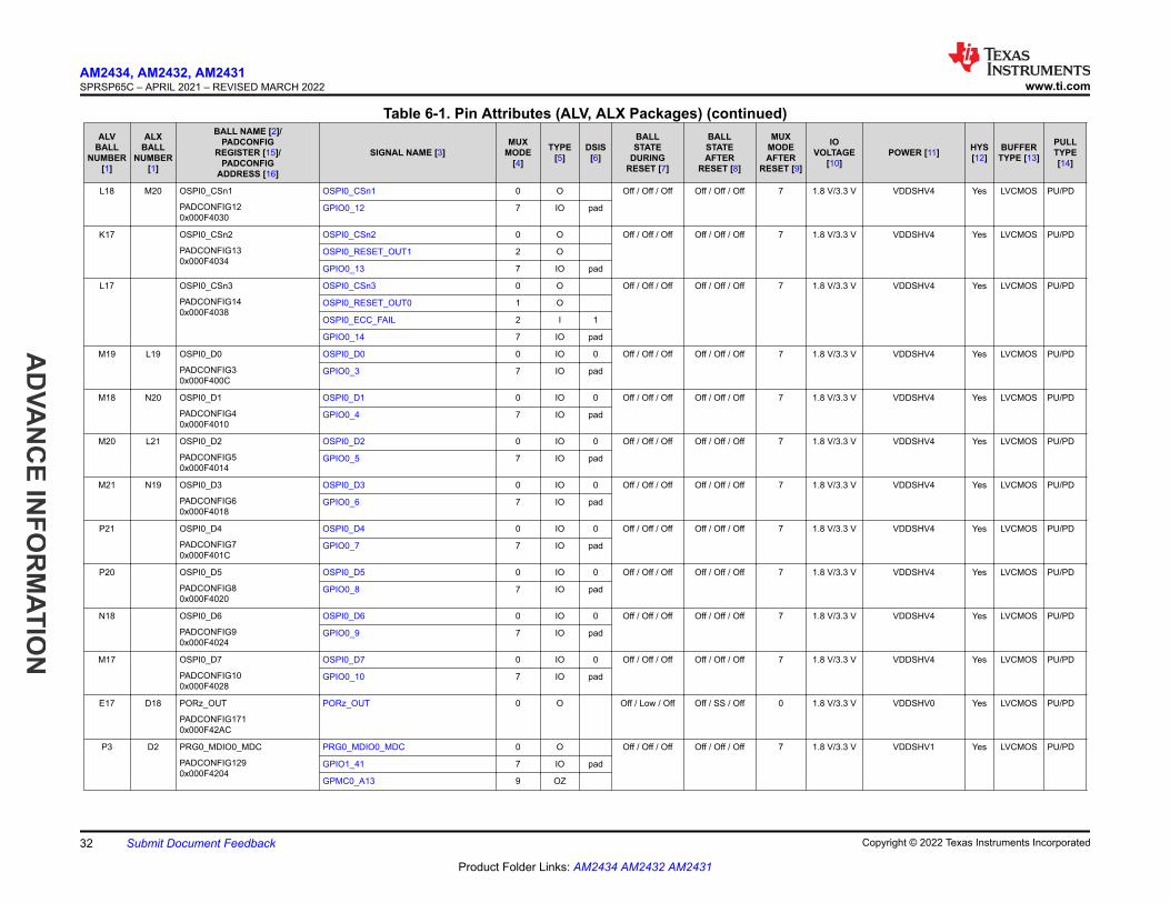
Table 6-1. Pin Attributes (ALV, ALX Packages) (continued)ALV
BALLNUMBER
[1]
ALX BALL
NUMBER [1]
BALL NAME [2]/PADCONFIG
REGISTER [15]/PADCONFIG
ADDRESS [16]
SIGNAL NAME [3]MUX
MODE [4]
TYPE [5]
DSIS [6]
BALLSTATE
DURINGRESET [7]
BALLSTATEAFTER
RESET [8]
MUXMODEAFTER
RESET [9]
IOVOLTAGE
[10]POWER [11] HYS
[12]BUFFER
TYPE [13]
PULLTYPE [14]
L18 M20 OSPI0_CSn1
PADCONFIG120x000F4030
OSPI0_CSn1 0 O Off / Off / Off Off / Off / Off 7 1.8 V/3.3 V VDDSHV4 Yes LVCMOS PU/PD
GPIO0_12 7 IO pad
K17 OSPI0_CSn2
PADCONFIG130x000F4034
OSPI0_CSn2 0 O Off / Off / Off Off / Off / Off 7 1.8 V/3.3 V VDDSHV4 Yes LVCMOS PU/PD
OSPI0_RESET_OUT1 2 O
GPIO0_13 7 IO pad
L17 OSPI0_CSn3
PADCONFIG140x000F4038
OSPI0_CSn3 0 O Off / Off / Off Off / Off / Off 7 1.8 V/3.3 V VDDSHV4 Yes LVCMOS PU/PD
OSPI0_RESET_OUT0 1 O
OSPI0_ECC_FAIL 2 I 1
GPIO0_14 7 IO pad
M19 L19 OSPI0_D0
PADCONFIG30x000F400C
OSPI0_D0 0 IO 0 Off / Off / Off Off / Off / Off 7 1.8 V/3.3 V VDDSHV4 Yes LVCMOS PU/PD
GPIO0_3 7 IO pad
M18 N20 OSPI0_D1
PADCONFIG40x000F4010
OSPI0_D1 0 IO 0 Off / Off / Off Off / Off / Off 7 1.8 V/3.3 V VDDSHV4 Yes LVCMOS PU/PD
GPIO0_4 7 IO pad
M20 L21 OSPI0_D2
PADCONFIG50x000F4014
OSPI0_D2 0 IO 0 Off / Off / Off Off / Off / Off 7 1.8 V/3.3 V VDDSHV4 Yes LVCMOS PU/PD
GPIO0_5 7 IO pad
M21 N19 OSPI0_D3
PADCONFIG60x000F4018
OSPI0_D3 0 IO 0 Off / Off / Off Off / Off / Off 7 1.8 V/3.3 V VDDSHV4 Yes LVCMOS PU/PD
GPIO0_6 7 IO pad
P21 OSPI0_D4
PADCONFIG70x000F401C
OSPI0_D4 0 IO 0 Off / Off / Off Off / Off / Off 7 1.8 V/3.3 V VDDSHV4 Yes LVCMOS PU/PD
GPIO0_7 7 IO pad
P20 OSPI0_D5
PADCONFIG80x000F4020
OSPI0_D5 0 IO 0 Off / Off / Off Off / Off / Off 7 1.8 V/3.3 V VDDSHV4 Yes LVCMOS PU/PD
GPIO0_8 7 IO pad
N18 OSPI0_D6
PADCONFIG90x000F4024
OSPI0_D6 0 IO 0 Off / Off / Off Off / Off / Off 7 1.8 V/3.3 V VDDSHV4 Yes LVCMOS PU/PD
GPIO0_9 7 IO pad
M17 OSPI0_D7
PADCONFIG100x000F4028
OSPI0_D7 0 IO 0 Off / Off / Off Off / Off / Off 7 1.8 V/3.3 V VDDSHV4 Yes LVCMOS PU/PD
GPIO0_10 7 IO pad
E17 D18 PORz_OUT
PADCONFIG1710x000F42AC
PORz_OUT 0 O Off / Low / Off Off / SS / Off 0 1.8 V/3.3 V VDDSHV0 Yes LVCMOS PU/PD
P3 D2 PRG0_MDIO0_MDC
PADCONFIG1290x000F4204
PRG0_MDIO0_MDC 0 O Off / Off / Off Off / Off / Off 7 1.8 V/3.3 V VDDSHV1 Yes LVCMOS PU/PD
GPIO1_41 7 IO pad
GPMC0_A13 9 OZ
AM2434, AM2432, AM2431SPRSP65C – APRIL 2021 – REVISED MARCH 2022 www.ti.com
AD
VAN
CE IN
FOR
MATIO
N
32 Submit Document Feedback Copyright © 2022 Texas Instruments Incorporated
Product Folder Links: AM2434 AM2432 AM2431

Table 6-1. Pin Attributes (ALV, ALX Packages) (continued)ALV
BALLNUMBER
[1]
ALX BALL
NUMBER [1]
BALL NAME [2]/PADCONFIG
REGISTER [15]/PADCONFIG
ADDRESS [16]
SIGNAL NAME [3]MUX
MODE [4]
TYPE [5]
DSIS [6]
BALLSTATE
DURINGRESET [7]
BALLSTATEAFTER
RESET [8]
MUXMODEAFTER
RESET [9]
IOVOLTAGE
[10]POWER [11] HYS
[12]BUFFER
TYPE [13]
PULLTYPE [14]
P2 E4 PRG0_MDIO0_MDIO
PADCONFIG1280x000F4200
PRG0_MDIO0_MDIO 0 IO 0 Off / Off / Off Off / Off / Off 7 1.8 V/3.3 V VDDSHV1 Yes LVCMOS PU/PD
GPIO1_40 7 IO pad
GPMC0_A12 9 OZ
Y1 J3 PRG0_PRU0_GPO0
PADCONFIG880x000F4160
PRG0_PRU0_GPO0 0 IO 0 Off / Off / Off Off / Off / Off 7 1.8 V/3.3 V VDDSHV1 Yes LVCMOS PU/PD
PRG0_PRU0_GPI0 1 I 0
PRG0_RGMII1_RD0 2 I 0
PRG0_PWM3_A0 3 IO 0
GPIO1_0 7 IO pad
UART2_CTSn 10 I 1
R4 J4 PRG0_PRU0_GPO1
PADCONFIG890x000F4164
PRG0_PRU0_GPO1 0 IO 0 Off / Off / Off Off / Off / Off 7 1.8 V/3.3 V VDDSHV1 Yes LVCMOS PU/PD
PRG0_PRU0_GPI1 1 I 0
PRG0_RGMII1_RD1 2 I 0
PRG0_PWM3_B0 3 IO 1
GPIO1_1 7 IO pad
UART2_TXD 10 O
U2 G1 PRG0_PRU0_GPO2
PADCONFIG900x000F4168
PRG0_PRU0_GPO2 0 IO 0 Off / Off / Off Off / Off / Off 7 1.8 V/3.3 V VDDSHV1 Yes LVCMOS PU/PD
PRG0_PRU0_GPI2 1 I 0
PRG0_RGMII1_RD2 2 I 0
PRG0_PWM2_A0 3 IO 0
GPIO1_2 7 IO pad
GPMC0_A0 9 OZ
UART2_RTSn 10 O
V2 H1 PRG0_PRU0_GPO3
PADCONFIG910x000F416C
PRG0_PRU0_GPO3 0 IO 0 Off / Off / Off Off / Off / Off 7 1.8 V/3.3 V VDDSHV1 Yes LVCMOS PU/PD
PRG0_PRU0_GPI3 1 I 0
PRG0_RGMII1_RD3 2 I 0
PRG0_PWM3_A2 3 IO 0
GPIO1_3 7 IO pad
UART3_CTSn 10 I 1
AA2 K2 PRG0_PRU0_GPO4
PADCONFIG920x000F4170
PRG0_PRU0_GPO4 0 IO 0 Off / Off / Off Off / Off / Off 7 1.8 V/3.3 V VDDSHV1 Yes LVCMOS PU/PD
PRG0_PRU0_GPI4 1 I 0
PRG0_RGMII1_RX_CTL 2 I 0
PRG0_PWM2_B0 3 IO 1
GPIO1_4 7 IO pad
GPMC0_A1 9 OZ
UART3_TXD 10 O
www.ti.comAM2434, AM2432, AM2431
SPRSP65C – APRIL 2021 – REVISED MARCH 2022
AD
VAN
CE
INFO
RM
ATIO
N
Copyright © 2022 Texas Instruments Incorporated Submit Document Feedback 33
Product Folder Links: AM2434 AM2432 AM2431

Table 6-1. Pin Attributes (ALV, ALX Packages) (continued)ALV
BALLNUMBER
[1]
ALX BALL
NUMBER [1]
BALL NAME [2]/PADCONFIG
REGISTER [15]/PADCONFIG
ADDRESS [16]
SIGNAL NAME [3]MUX
MODE [4]
TYPE [5]
DSIS [6]
BALLSTATE
DURINGRESET [7]
BALLSTATEAFTER
RESET [8]
MUXMODEAFTER
RESET [9]
IOVOLTAGE
[10]POWER [11] HYS
[12]BUFFER
TYPE [13]
PULLTYPE [14]
R3 F2 PRG0_PRU0_GPO5
PADCONFIG930x000F4174
PRG0_PRU0_GPO5 0 IO 0 Off / Off / Off Off / Off / Off 7 1.8 V/3.3 V VDDSHV1 Yes LVCMOS PU/PD
PRG0_PRU0_GPI5 1 I 0
PRG0_PWM3_B2 3 IO 1
GPIO1_5 7 IO pad
UART3_RTSn 10 O
T3 H2 PRG0_PRU0_GPO6
PADCONFIG940x000F4178
PRG0_PRU0_GPO6 0 IO 0 Off / Off / Off Off / Off / Off 7 1.8 V/3.3 V VDDSHV1 Yes LVCMOS PU/PD
PRG0_PRU0_GPI6 1 I 0
PRG0_RGMII1_RXC 2 I 0
PRG0_PWM3_A1 3 IO 0
GPIO1_6 7 IO pad
UART4_CTSn 10 I 1
T1 E2 PRG0_PRU0_GPO7
PADCONFIG950x000F417C
PRG0_PRU0_GPO7 0 IO 0 Off / Off / Off Off / Off / Off 7 1.8 V/3.3 V VDDSHV1 Yes LVCMOS PU/PD
PRG0_PRU0_GPI7 1 I 0
PRG0_IEP0_EDC_LATCH_IN1 2 I 0
PRG0_PWM3_B1 3 IO 1
CPTS0_HW2TSPUSH 4 I 0
CP_GEMAC_CPTS0_HW2TSPUSH 5 I 0
TIMER_IO6 6 IO 0
GPIO1_7 7 IO pad
UART4_TXD 10 O
T2 H5 PRG0_PRU0_GPO8
PADCONFIG960x000F4180
PRG0_PRU0_GPO8 0 IO 0 Off / Off / Off Off / Off / Off 7 1.8 V/3.3 V VDDSHV1 Yes LVCMOS PU/PD
PRG0_PRU0_GPI8 1 I 0
PRG0_PWM2_A1 3 IO 0
GPIO1_8 7 IO pad
GPMC0_A2 9 OZ
UART4_RTSn 10 O
W6 Y3 PRG0_PRU0_GPO9
PADCONFIG970x000F4184
PRG0_PRU0_GPO9 0 IO 0 Off / Off / Off Off / Off / Off 7 1.8 V/3.3 V VDDSHV1 Yes LVCMOS PU/PD
PRG0_PRU0_GPI9 1 I 0
PRG0_UART0_CTSn 2 I 1
PRG0_PWM3_TZ_IN 3 I 0
RGMII1_RX_CTL 4 I 0
RMII1_RX_ER 5 I 0
PRG0_IEP0_EDIO_DATA_IN_OUT28 6 IO 0
GPIO1_9 7 IO pad
UART2_RXD 10 I 1
AM2434, AM2432, AM2431SPRSP65C – APRIL 2021 – REVISED MARCH 2022 www.ti.com
AD
VAN
CE IN
FOR
MATIO
N
34 Submit Document Feedback Copyright © 2022 Texas Instruments Incorporated
Product Folder Links: AM2434 AM2432 AM2431

Table 6-1. Pin Attributes (ALV, ALX Packages) (continued)ALV
BALLNUMBER
[1]
ALX BALL
NUMBER [1]
BALL NAME [2]/PADCONFIG
REGISTER [15]/PADCONFIG
ADDRESS [16]
SIGNAL NAME [3]MUX
MODE [4]
TYPE [5]
DSIS [6]
BALLSTATE
DURINGRESET [7]
BALLSTATEAFTER
RESET [8]
MUXMODEAFTER
RESET [9]
IOVOLTAGE
[10]POWER [11] HYS
[12]BUFFER
TYPE [13]
PULLTYPE [14]
AA5 U1 PRG0_PRU0_GPO10
PADCONFIG980x000F4188
PRG0_PRU0_GPO10 0 IO 0 Off / Off / Off Off / Off / Off 7 1.8 V/3.3 V VDDSHV1 Yes LVCMOS PU/PD
PRG0_PRU0_GPI10 1 I 0
PRG0_UART0_RTSn 2 O
PRG0_PWM2_B1 3 IO 1
RGMII1_RXC 4 I 0
RMII_REF_CLK 5 I 0
PRG0_IEP0_EDIO_DATA_IN_OUT29 6 IO 0
GPIO1_10 7 IO pad
UART3_RXD 10 I 1
Y3 L1 PRG0_PRU0_GPO11
PADCONFIG990x000F418C
PRG0_PRU0_GPO11 0 IO 0 Off / Off / Off Off / Off / Off 7 1.8 V/3.3 V VDDSHV1 Yes LVCMOS PU/PD
PRG0_PRU0_GPI11 1 I 0
PRG0_RGMII1_TD0 2 O
PRG0_PWM3_TZ_OUT 3 O
GPIO1_11 7 IO pad
UART4_RXD 10 I 1
AA3 K1 PRG0_PRU0_GPO12
PADCONFIG1000x000F4190
PRG0_PRU0_GPO12 0 IO 0 Off / Off / Off Off / Off / Off 7 1.8 V/3.3 V VDDSHV1 Yes LVCMOS PU/PD
PRG0_PRU0_GPI12 1 I 0
PRG0_RGMII1_TD1 2 O
PRG0_PWM0_A0 3 IO 0
GPIO1_12 7 IO pad
GPMC0_A14 9 OZ
R6 N1 PRG0_PRU0_GPO13
PADCONFIG1010x000F4194
PRG0_PRU0_GPO13 0 IO 0 Off / Off / Off Off / Off / Off 7 1.8 V/3.3 V VDDSHV1 Yes LVCMOS PU/PD
PRG0_PRU0_GPI13 1 I 0
PRG0_RGMII1_TD2 2 O
PRG0_PWM0_B0 3 IO 1
SPI3_D0 6 IO 0
GPIO1_13 7 IO pad
GPMC0_A15 9 OZ
V4 N2 PRG0_PRU0_GPO14
PADCONFIG1020x000F4198
PRG0_PRU0_GPO14 0 IO 0 Off / Off / Off Off / Off / Off 7 1.8 V/3.3 V VDDSHV1 Yes LVCMOS PU/PD
PRG0_PRU0_GPI14 1 I 0
PRG0_RGMII1_TD3 2 O
PRG0_PWM0_A1 3 IO 0
SPI3_D1 6 IO 0
GPIO1_14 7 IO pad
GPMC0_A3 9 OZ
www.ti.comAM2434, AM2432, AM2431
SPRSP65C – APRIL 2021 – REVISED MARCH 2022
AD
VAN
CE
INFO
RM
ATIO
N
Copyright © 2022 Texas Instruments Incorporated Submit Document Feedback 35
Product Folder Links: AM2434 AM2432 AM2431

Table 6-1. Pin Attributes (ALV, ALX Packages) (continued)ALV
BALLNUMBER
[1]
ALX BALL
NUMBER [1]
BALL NAME [2]/PADCONFIG
REGISTER [15]/PADCONFIG
ADDRESS [16]
SIGNAL NAME [3]MUX
MODE [4]
TYPE [5]
DSIS [6]
BALLSTATE
DURINGRESET [7]
BALLSTATEAFTER
RESET [8]
MUXMODEAFTER
RESET [9]
IOVOLTAGE
[10]POWER [11] HYS
[12]BUFFER
TYPE [13]
PULLTYPE [14]
T5 N4 PRG0_PRU0_GPO15
PADCONFIG1030x000F419C
PRG0_PRU0_GPO15 0 IO 0 Off / Off / Off Off / Off / Off 7 1.8 V/3.3 V VDDSHV1 Yes LVCMOS PU/PD
PRG0_PRU0_GPI15 1 I 0
PRG0_RGMII1_TX_CTL 2 O
PRG0_PWM0_B1 3 IO 1
SPI3_CS1 6 IO 1
GPIO1_15 7 IO pad
GPMC0_A16 9 OZ
U4 N3 PRG0_PRU0_GPO16
PADCONFIG1040x000F41A0
PRG0_PRU0_GPO16 0 IO 0 Off / Off / Off Off / Off / Off 7 1.8 V/3.3 V VDDSHV1 Yes LVCMOS PU/PD
PRG0_PRU0_GPI16 1 I 0
PRG0_RGMII1_TXC 2 IO 0
PRG0_PWM0_A2 3 IO 0
SPI3_CLK 6 IO 0
GPIO1_16 7 IO pad
GPMC0_A4 9 OZ
U1 E1 PRG0_PRU0_GPO17
PADCONFIG1050x000F41A4
PRG0_PRU0_GPO17 0 IO 0 Off / Off / Off Off / Off / Off 7 1.8 V/3.3 V VDDSHV1 Yes LVCMOS PU/PD
PRG0_PRU0_GPI17 1 I 0
PRG0_IEP0_EDC_SYNC_OUT1 2 O
PRG0_PWM0_B2 3 IO 1
CPTS0_TS_SYNC 4 O
CP_GEMAC_CPTS0_TS_SYNC 5 O
SPI3_CS0 6 IO 1
GPIO1_17 7 IO pad
TIMER_IO11 8 IO 0
GPMC0_A17 9 OZ
V1 K4 PRG0_PRU0_GPO18
PADCONFIG1060x000F41A8
PRG0_PRU0_GPO18 0 IO 0 Off / Off / Off Off / Off / Off 7 1.8 V/3.3 V VDDSHV1 Yes LVCMOS PU/PD
PRG0_PRU0_GPI18 1 I 0
PRG0_IEP0_EDC_LATCH_IN0 2 I 0
PRG0_PWM0_TZ_IN 3 I 0
CPTS0_HW1TSPUSH 4 I 0
CP_GEMAC_CPTS0_HW1TSPUSH 5 I 0
EHRPWM8_A 6 IO 0
GPIO1_18 7 IO pad
UART4_CTSn 8 I 1
GPMC0_A5 9 OZ
UART2_RXD 10 I 1
AM2434, AM2432, AM2431SPRSP65C – APRIL 2021 – REVISED MARCH 2022 www.ti.com
AD
VAN
CE IN
FOR
MATIO
N
36 Submit Document Feedback Copyright © 2022 Texas Instruments Incorporated
Product Folder Links: AM2434 AM2432 AM2431

Table 6-1. Pin Attributes (ALV, ALX Packages) (continued)ALV
BALLNUMBER
[1]
ALX BALL
NUMBER [1]
BALL NAME [2]/PADCONFIG
REGISTER [15]/PADCONFIG
ADDRESS [16]
SIGNAL NAME [3]MUX
MODE [4]
TYPE [5]
DSIS [6]
BALLSTATE
DURINGRESET [7]
BALLSTATEAFTER
RESET [8]
MUXMODEAFTER
RESET [9]
IOVOLTAGE
[10]POWER [11] HYS
[12]BUFFER
TYPE [13]
PULLTYPE [14]
W1 G2 PRG0_PRU0_GPO19
PADCONFIG1070x000F41AC
PRG0_PRU0_GPO19 0 IO 0 Off / Off / Off Off / Off / Off 7 1.8 V/3.3 V VDDSHV1 Yes LVCMOS PU/PD
PRG0_PRU0_GPI19 1 I 0
PRG0_IEP0_EDC_SYNC_OUT0 2 O
PRG0_PWM0_TZ_OUT 3 O
CPTS0_TS_COMP 4 O
CP_GEMAC_CPTS0_TS_COMP 5 O
EHRPWM8_B 6 IO 0
GPIO1_19 7 IO pad
UART4_RTSn 8 O
GPMC0_A6 9 OZ
UART3_RXD 10 I 1
Y2 L5 PRG0_PRU1_GPO0
PADCONFIG1080x000F41B0
PRG0_PRU1_GPO0 0 IO 0 Off / Off / Off Off / Off / Off 7 1.8 V/3.3 V VDDSHV1 Yes LVCMOS PU/PD
PRG0_PRU1_GPI0 1 I 0
PRG0_RGMII2_RD0 2 I 0
GPIO1_20 7 IO pad
EQEP0_A 8 I 0
UART5_CTSn 10 I 1
W2 J2 PRG0_PRU1_GPO1
PADCONFIG1090x000F41B4
PRG0_PRU1_GPO1 0 IO 0 Off / Off / Off Off / Off / Off 7 1.8 V/3.3 V VDDSHV1 Yes LVCMOS PU/PD
PRG0_PRU1_GPI1 1 I 0
PRG0_RGMII2_RD1 2 I 0
GPIO1_21 7 IO pad
EQEP0_B 8 I 0
UART5_TXD 10 O
V3 M2 PRG0_PRU1_GPO2
PADCONFIG1100x000F41B8
PRG0_PRU1_GPO2 0 IO 0 Off / Off / Off Off / Off / Off 7 1.8 V/3.3 V VDDSHV1 Yes LVCMOS PU/PD
PRG0_PRU1_GPI2 1 I 0
PRG0_RGMII2_RD2 2 I 0
PRG0_PWM2_A2 3 IO 0
GPIO1_22 7 IO pad
EQEP0_S 8 IO 0
UART5_RTSn 10 O
T4 L2 PRG0_PRU1_GPO3
PADCONFIG1110x000F41BC
PRG0_PRU1_GPO3 0 IO 0 Off / Off / Off Off / Off / Off 7 1.8 V/3.3 V VDDSHV1 Yes LVCMOS PU/PD
PRG0_PRU1_GPI3 1 I 0
PRG0_RGMII2_RD3 2 I 0
GPIO1_23 7 IO pad
EQEP1_A 8 I 0
GPMC0_A18 9 OZ
UART6_CTSn 10 I 1
www.ti.comAM2434, AM2432, AM2431
SPRSP65C – APRIL 2021 – REVISED MARCH 2022
AD
VAN
CE
INFO
RM
ATIO
N
Copyright © 2022 Texas Instruments Incorporated Submit Document Feedback 37
Product Folder Links: AM2434 AM2432 AM2431

Table 6-1. Pin Attributes (ALV, ALX Packages) (continued)ALV
BALLNUMBER
[1]
ALX BALL
NUMBER [1]
BALL NAME [2]/PADCONFIG
REGISTER [15]/PADCONFIG
ADDRESS [16]
SIGNAL NAME [3]MUX
MODE [4]
TYPE [5]
DSIS [6]
BALLSTATE
DURINGRESET [7]
BALLSTATEAFTER
RESET [8]
MUXMODEAFTER
RESET [9]
IOVOLTAGE
[10]POWER [11] HYS
[12]BUFFER
TYPE [13]
PULLTYPE [14]
W3 L3 PRG0_PRU1_GPO4
PADCONFIG1120x000F41C0
PRG0_PRU1_GPO4 0 IO 0 Off / Off / Off Off / Off / Off 7 1.8 V/3.3 V VDDSHV1 Yes LVCMOS PU/PD
PRG0_PRU1_GPI4 1 I 0
PRG0_RGMII2_RX_CTL 2 I 0
PRG0_PWM2_B2 3 IO 1
GPIO1_24 7 IO pad
EQEP1_B 8 I 0
UART6_TXD 10 O
P4 E3 PRG0_PRU1_GPO5
PADCONFIG1130x000F41C4
PRG0_PRU1_GPO5 0 IO 0 Off / Off / Off Off / Off / Off 7 1.8 V/3.3 V VDDSHV1 Yes LVCMOS PU/PD
PRG0_PRU1_GPI5 1 I 0
GPIO1_25 7 IO pad
EQEP1_S 8 IO 0
UART6_RTSn 10 O
R5 F5 PRG0_PRU1_GPO6
PADCONFIG1140x000F41C8
PRG0_PRU1_GPO6 0 IO 0 Off / Off / Off Off / Off / Off 7 1.8 V/3.3 V VDDSHV1 Yes LVCMOS PU/PD
PRG0_PRU1_GPI6 1 I 0
PRG0_RGMII2_RXC 2 I 0
GPIO1_26 7 IO pad
EQEP2_A 8 I 0
GPMC0_A19 9 OZ
UART4_CTSn 10 I 1
W5 T5 PRG0_PRU1_GPO7
PADCONFIG1150x000F41CC
PRG0_PRU1_GPO7 0 IO 0 Off / Off / Off Off / Off / Off 7 1.8 V/3.3 V VDDSHV1 Yes LVCMOS PU/PD
PRG0_PRU1_GPI7 1 I 0
PRG0_IEP1_EDC_LATCH_IN1 2 I 0
RGMII1_RD0 4 I 0
RMII1_RXD0 5 I 0
GPIO1_27 7 IO pad
EQEP2_B 8 I 0
UART4_TXD 10 O
R1 F4 PRG0_PRU1_GPO8
PADCONFIG1160x000F41D0
PRG0_PRU1_GPO8 0 IO 0 Off / Off / Off Off / Off / Off 7 1.8 V/3.3 V VDDSHV1 Yes LVCMOS PU/PD
PRG0_PRU1_GPI8 1 I 0
PRG0_PWM2_TZ_OUT 3 O
GPIO1_28 7 IO pad
EQEP2_S 8 IO 0
UART4_RTSn 10 O
AM2434, AM2432, AM2431SPRSP65C – APRIL 2021 – REVISED MARCH 2022 www.ti.com
AD
VAN
CE IN
FOR
MATIO
N
38 Submit Document Feedback Copyright © 2022 Texas Instruments Incorporated
Product Folder Links: AM2434 AM2432 AM2431

Table 6-1. Pin Attributes (ALV, ALX Packages) (continued)ALV
BALLNUMBER
[1]
ALX BALL
NUMBER [1]
BALL NAME [2]/PADCONFIG
REGISTER [15]/PADCONFIG
ADDRESS [16]
SIGNAL NAME [3]MUX
MODE [4]
TYPE [5]
DSIS [6]
BALLSTATE
DURINGRESET [7]
BALLSTATEAFTER
RESET [8]
MUXMODEAFTER
RESET [9]
IOVOLTAGE
[10]POWER [11] HYS
[12]BUFFER
TYPE [13]
PULLTYPE [14]
Y5 R2 PRG0_PRU1_GPO9
PADCONFIG1170x000F41D4
PRG0_PRU1_GPO9 0 IO 0 Off / Off / Off Off / Off / Off 7 1.8 V/3.3 V VDDSHV1 Yes LVCMOS PU/PD
PRG0_PRU1_GPI9 1 I 0
PRG0_UART0_RXD 2 I 1
RGMII1_RD1 4 I 0
RMII1_RXD1 5 I 0
PRG0_IEP0_EDIO_DATA_IN_OUT30 6 IO 0
GPIO1_29 7 IO pad
EQEP0_I 8 IO 0
UART5_RXD 10 I 1
V6 U2 PRG0_PRU1_GPO10
PADCONFIG1180x000F41D8
PRG0_PRU1_GPO10 0 IO 0 Off / Off / Off Off / Off / Off 7 1.8 V/3.3 V VDDSHV1 Yes LVCMOS PU/PD
PRG0_PRU1_GPI10 1 I 0
PRG0_UART0_TXD 2 O
PRG0_PWM2_TZ_IN 3 I 0
RGMII1_RD2 4 I 0
RMII1_TXD0 5 O
PRG0_IEP0_EDIO_DATA_IN_OUT31 6 IO 0
GPIO1_30 7 IO pad
EQEP1_I 8 IO 0
UART6_RXD 10 I 1
W4 P1 PRG0_PRU1_GPO11
PADCONFIG1190x000F41DC
PRG0_PRU1_GPO11 0 IO 0 Off / Off / Off Off / Off / Off 7 1.8 V/3.3 V VDDSHV1 Yes LVCMOS PU/PD
PRG0_PRU1_GPI11 1 I 0
PRG0_RGMII2_TD0 2 O
GPIO1_31 7 IO pad
EQEP2_I 8 IO 0
UART4_RXD 10 I 1
Y4 P2 PRG0_PRU1_GPO12
PADCONFIG1200x000F41E0
PRG0_PRU1_GPO12 0 IO 0 Off / Off / Off Off / Off / Off 7 1.8 V/3.3 V VDDSHV1 Yes LVCMOS PU/PD
PRG0_PRU1_GPI12 1 I 0
PRG0_RGMII2_TD1 2 O
PRG0_PWM1_A0 3 IO 0
GPIO1_32 7 IO pad
EQEP2_B 8 I 0
GPMC0_A7 9 OZ
UART4_TXD 10 O
www.ti.comAM2434, AM2432, AM2431
SPRSP65C – APRIL 2021 – REVISED MARCH 2022
AD
VAN
CE
INFO
RM
ATIO
N
Copyright © 2022 Texas Instruments Incorporated Submit Document Feedback 39
Product Folder Links: AM2434 AM2432 AM2431

Table 6-1. Pin Attributes (ALV, ALX Packages) (continued)ALV
BALLNUMBER
[1]
ALX BALL
NUMBER [1]
BALL NAME [2]/PADCONFIG
REGISTER [15]/PADCONFIG
ADDRESS [16]
SIGNAL NAME [3]MUX
MODE [4]
TYPE [5]
DSIS [6]
BALLSTATE
DURINGRESET [7]
BALLSTATEAFTER
RESET [8]
MUXMODEAFTER
RESET [9]
IOVOLTAGE
[10]POWER [11] HYS
[12]BUFFER
TYPE [13]
PULLTYPE [14]
T6 T4 PRG0_PRU1_GPO13
PADCONFIG1210x000F41E4
PRG0_PRU1_GPO13 0 IO 0 Off / Off / Off Off / Off / Off 7 1.8 V/3.3 V VDDSHV1 Yes LVCMOS PU/PD
PRG0_PRU1_GPI13 1 I 0
PRG0_RGMII2_TD2 2 O
PRG0_PWM1_B0 3 IO 1
GPIO1_33 7 IO pad
EQEP0_I 8 IO 0
GPMC0_A8 9 OZ
UART5_RXD 10 I 1
U6 R5 PRG0_PRU1_GPO14
PADCONFIG1220x000F41E8
PRG0_PRU1_GPO14 0 IO 0 Off / Off / Off Off / Off / Off 7 1.8 V/3.3 V VDDSHV1 Yes LVCMOS PU/PD
PRG0_PRU1_GPI14 1 I 0
PRG0_RGMII2_TD3 2 O
PRG0_PWM1_A1 3 IO 0
GPIO1_34 7 IO pad
EQEP1_I 8 IO 0
GPMC0_A9 9 OZ
UART6_RXD 10 I 1
U5 M4 PRG0_PRU1_GPO15
PADCONFIG1230x000F41EC
PRG0_PRU1_GPO15 0 IO 0 Off / Off / Off Off / Off / Off 7 1.8 V/3.3 V VDDSHV1 Yes LVCMOS PU/PD
PRG0_PRU1_GPI15 1 I 0
PRG0_RGMII2_TX_CTL 2 O
PRG0_PWM1_B1 3 IO 1
GPIO1_35 7 IO pad
GPMC0_A10 9 OZ
PRG0_ECAP0_IN_APWM_OUT 10 IO 0
AA4 T3 PRG0_PRU1_GPO16
PADCONFIG1240x000F41F0
PRG0_PRU1_GPO16 0 IO 0 Off / Off / Off Off / Off / Off 7 1.8 V/3.3 V VDDSHV1 Yes LVCMOS PU/PD
PRG0_PRU1_GPI16 1 I 0
PRG0_RGMII2_TXC 2 IO 0
PRG0_PWM1_A2 3 IO 0
GPIO1_36 7 IO pad
GPMC0_A11 9 OZ
PRG0_ECAP0_SYNC_OUT 10 O
AM2434, AM2432, AM2431SPRSP65C – APRIL 2021 – REVISED MARCH 2022 www.ti.com
AD
VAN
CE IN
FOR
MATIO
N
40 Submit Document Feedback Copyright © 2022 Texas Instruments Incorporated
Product Folder Links: AM2434 AM2432 AM2431

Table 6-1. Pin Attributes (ALV, ALX Packages) (continued)ALV
BALLNUMBER
[1]
ALX BALL
NUMBER [1]
BALL NAME [2]/PADCONFIG
REGISTER [15]/PADCONFIG
ADDRESS [16]
SIGNAL NAME [3]MUX
MODE [4]
TYPE [5]
DSIS [6]
BALLSTATE
DURINGRESET [7]
BALLSTATEAFTER
RESET [8]
MUXMODEAFTER
RESET [9]
IOVOLTAGE
[10]POWER [11] HYS
[12]BUFFER
TYPE [13]
PULLTYPE [14]
V5 T1 PRG0_PRU1_GPO17
PADCONFIG1250x000F41F4
PRG0_PRU1_GPO17 0 IO 0 Off / Off / Off Off / Off / Off 7 1.8 V/3.3 V VDDSHV1 Yes LVCMOS PU/PD
PRG0_PRU1_GPI17 1 I 0
PRG0_IEP1_EDC_SYNC_OUT1 2 O
PRG0_PWM1_B2 3 IO 1
RGMII1_RD3 4 I 0
RMII1_TXD1 5 O
GPIO1_37 7 IO pad
PRG0_ECAP0_SYNC_OUT 8 O
PRG0_ECAP0_SYNC_IN 10 I 0
P5 D1 PRG0_PRU1_GPO18
PADCONFIG1260x000F41F8
PRG0_PRU1_GPO18 0 IO 0 Off / Off / Off Off / Off / Off 7 1.8 V/3.3 V VDDSHV1 Yes LVCMOS PU/PD
PRG0_PRU1_GPI18 1 I 0
PRG0_IEP1_EDC_LATCH_IN0 2 I 0
PRG0_PWM1_TZ_IN 3 I 0
MDIO0_MDIO 4 IO 0
RMII1_TX_EN 5 O
EHRPWM7_A 6 IO 0
GPIO1_38 7 IO pad
PRG0_ECAP0_SYNC_IN 8 I 0
R2 F3 PRG0_PRU1_GPO19
PADCONFIG1270x000F41FC
PRG0_PRU1_GPO19 0 IO 0 Off / Off / Off Off / Off / Off 7 1.8 V/3.3 V VDDSHV1 Yes LVCMOS PU/PD
PRG0_PRU1_GPI19 1 I 0
PRG0_IEP1_EDC_SYNC_OUT0 2 O
PRG0_PWM1_TZ_OUT 3 O
MDIO0_MDC 4 O
RMII1_CRS_DV 5 I 0
EHRPWM7_B 6 IO 0
GPIO1_39 7 IO pad
PRG0_ECAP0_IN_APWM_OUT 8 IO 0
Y6 W1 PRG1_MDIO0_MDC
PADCONFIG870x000F415C
PRG1_MDIO0_MDC 0 O Off / Off / Off Off / Off / Off 7 1.8 V/3.3 V VDDSHV2 Yes LVCMOS PU/PD
MDIO0_MDC 4 O
GPIO0_86 7 IO pad
AA6 V2 PRG1_MDIO0_MDIO
PADCONFIG860x000F4158
PRG1_MDIO0_MDIO 0 IO 0 Off / Off / Off Off / Off / Off 7 1.8 V/3.3 V VDDSHV2 Yes LVCMOS PU/PD
MDIO0_MDIO 4 IO 0
GPIO0_85 7 IO pad
www.ti.comAM2434, AM2432, AM2431
SPRSP65C – APRIL 2021 – REVISED MARCH 2022
AD
VAN
CE
INFO
RM
ATIO
N
Copyright © 2022 Texas Instruments Incorporated Submit Document Feedback 41
Product Folder Links: AM2434 AM2432 AM2431

Table 6-1. Pin Attributes (ALV, ALX Packages) (continued)ALV
BALLNUMBER
[1]
ALX BALL
NUMBER [1]
BALL NAME [2]/PADCONFIG
REGISTER [15]/PADCONFIG
ADDRESS [16]
SIGNAL NAME [3]MUX
MODE [4]
TYPE [5]
DSIS [6]
BALLSTATE
DURINGRESET [7]
BALLSTATEAFTER
RESET [8]
MUXMODEAFTER
RESET [9]
IOVOLTAGE
[10]POWER [11] HYS
[12]BUFFER
TYPE [13]
PULLTYPE [14]
Y7 V4 PRG1_PRU0_GPO0
PADCONFIG460x000F40B8
PRG1_PRU0_GPO0 0 IO 0 Off / Off / Off Off / Off / Off 7 1.8 V/3.3 V VDDSHV2 Yes LVCMOS PU/PD
PRG1_PRU0_GPI0 1 I 0
PRG1_RGMII1_RD0 2 I 0
PRG1_PWM3_A0 3 IO 0
GPIO0_45 7 IO pad
GPMC0_AD16 8 IO 0
U8 W5 PRG1_PRU0_GPO1
PADCONFIG470x000F40BC
PRG1_PRU0_GPO1 0 IO 0 Off / Off / Off Off / Off / Off 7 1.8 V/3.3 V VDDSHV2 Yes LVCMOS PU/PD
PRG1_PRU0_GPI1 1 I 0
PRG1_RGMII1_RD1 2 I 0
PRG1_PWM3_B0 3 IO 1
GPIO0_46 7 IO pad
GPMC0_AD17 8 IO 0
W8 AA4 PRG1_PRU0_GPO2
PADCONFIG480x000F40C0
PRG1_PRU0_GPO2 0 IO 0 Off / Off / Off Off / Off / Off 7 1.8 V/3.3 V VDDSHV2 Yes LVCMOS PU/PD
PRG1_PRU0_GPI2 1 I 0
PRG1_RGMII1_RD2 2 I 0
PRG1_PWM2_A0 3 IO 0
GPIO0_47 7 IO pad
GPMC0_AD18 8 IO 0
V8 Y5 PRG1_PRU0_GPO3
PADCONFIG490x000F40C4
PRG1_PRU0_GPO3 0 IO 0 Off / Off / Off Off / Off / Off 7 1.8 V/3.3 V VDDSHV2 Yes LVCMOS PU/PD
PRG1_PRU0_GPI3 1 I 0
PRG1_RGMII1_RD3 2 I 0
PRG1_PWM3_A2 3 IO 0
GPIO0_48 7 IO pad
GPMC0_AD19 8 IO 0
Y8 AA5 PRG1_PRU0_GPO4
PADCONFIG500x000F40C8
PRG1_PRU0_GPO4 0 IO 0 Off / Off / Off Off / Off / Off 7 1.8 V/3.3 V VDDSHV2 Yes LVCMOS PU/PD
PRG1_PRU0_GPI4 1 I 0
PRG1_RGMII1_RX_CTL 2 I 0
PRG1_PWM2_B0 3 IO 1
GPIO0_49 7 IO pad
GPMC0_AD20 8 IO 0
V13 U14 PRG1_PRU0_GPO5
PADCONFIG510x000F40CC
PRG1_PRU0_GPO5 0 IO 0 Off / Off / Off Off / Off / Off 7 1.8 V/3.3 V VDDSHV2 Yes LVCMOS PU/PD
PRG1_PRU0_GPI5 1 I 0
PRG1_PWM3_B2 3 IO 1
RGMII1_RX_CTL 4 I 0
GPIO0_50 7 IO pad
GPMC0_AD21 8 IO 0
AM2434, AM2432, AM2431SPRSP65C – APRIL 2021 – REVISED MARCH 2022 www.ti.com
AD
VAN
CE IN
FOR
MATIO
N
42 Submit Document Feedback Copyright © 2022 Texas Instruments Incorporated
Product Folder Links: AM2434 AM2432 AM2431

Table 6-1. Pin Attributes (ALV, ALX Packages) (continued)ALV
BALLNUMBER
[1]
ALX BALL
NUMBER [1]
BALL NAME [2]/PADCONFIG
REGISTER [15]/PADCONFIG
ADDRESS [16]
SIGNAL NAME [3]MUX
MODE [4]
TYPE [5]
DSIS [6]
BALLSTATE
DURINGRESET [7]
BALLSTATEAFTER
RESET [8]
MUXMODEAFTER
RESET [9]
IOVOLTAGE
[10]POWER [11] HYS
[12]BUFFER
TYPE [13]
PULLTYPE [14]
AA7 Y2 PRG1_PRU0_GPO6
PADCONFIG520x000F40D0
PRG1_PRU0_GPO6 0 IO 0 Off / Off / Off Off / Off / Off 7 1.8 V/3.3 V VDDSHV2 Yes LVCMOS PU/PD
PRG1_PRU0_GPI6 1 I 0
PRG1_RGMII1_RXC 2 I 0
PRG1_PWM3_A1 3 IO 0
GPIO0_51 7 IO pad
GPMC0_AD22 8 IO 0
U13 V13 PRG1_PRU0_GPO7
PADCONFIG530x000F40D4
PRG1_PRU0_GPO7 0 IO 0 Off / Off / Off Off / Off / Off 7 1.8 V/3.3 V VDDSHV2 Yes LVCMOS PU/PD
PRG1_PRU0_GPI7 1 I 0
PRG1_IEP0_EDC_LATCH_IN1 2 I 0
PRG1_PWM3_B1 3 IO 1
CPTS0_HW2TSPUSH 4 I 0
CLKOUT0 5 O
TIMER_IO10 6 IO 0
GPIO0_52 7 IO pad
GPMC0_AD23 8 IO 0
W13 Y13 PRG1_PRU0_GPO8
PADCONFIG540x000F40D8
PRG1_PRU0_GPO8 0 IO 0 Off / Off / Off Off / Off / Off 7 1.8 V/3.3 V VDDSHV2 Yes LVCMOS PU/PD
PRG1_PRU0_GPI8 1 I 0
PRG1_PWM2_A1 3 IO 0
RGMII1_RXC 4 I 0
GPIO0_53 7 IO pad
GPMC0_AD24 8 IO 0
U15 W16 PRG1_PRU0_GPO9
PADCONFIG550x000F40DC
PRG1_PRU0_GPO9 0 IO 0 Off / Off / Off Off / Off / Off 7 1.8 V/3.3 V VDDSHV2 Yes LVCMOS PU/PD
PRG1_PRU0_GPI9 1 I 0
PRG1_UART0_CTSn 2 I 1
PRG1_PWM3_TZ_IN 3 I 0
RGMII1_TX_CTL 4 O
RMII1_RX_ER 5 I 0
PRG1_IEP0_EDIO_DATA_IN_OUT28 6 IO 0
GPIO0_54 7 IO pad
GPMC0_AD25 8 IO 0
www.ti.comAM2434, AM2432, AM2431
SPRSP65C – APRIL 2021 – REVISED MARCH 2022
AD
VAN
CE
INFO
RM
ATIO
N
Copyright © 2022 Texas Instruments Incorporated Submit Document Feedback 43
Product Folder Links: AM2434 AM2432 AM2431

Table 6-1. Pin Attributes (ALV, ALX Packages) (continued)ALV
BALLNUMBER
[1]
ALX BALL
NUMBER [1]
BALL NAME [2]/PADCONFIG
REGISTER [15]/PADCONFIG
ADDRESS [16]
SIGNAL NAME [3]MUX
MODE [4]
TYPE [5]
DSIS [6]
BALLSTATE
DURINGRESET [7]
BALLSTATEAFTER
RESET [8]
MUXMODEAFTER
RESET [9]
IOVOLTAGE
[10]POWER [11] HYS
[12]BUFFER
TYPE [13]
PULLTYPE [14]
U14 W13 PRG1_PRU0_GPO10
PADCONFIG560x000F40E0
PRG1_PRU0_GPO10 0 IO 0 Off / Off / Off Off / Off / Off 7 1.8 V/3.3 V VDDSHV2 Yes LVCMOS PU/PD
PRG1_PRU0_GPI10 1 I 0
PRG1_UART0_RTSn 2 O
PRG1_PWM2_B1 3 IO 1
RGMII1_TXC 4 IO 0
RMII_REF_CLK 5 I 0
PRG1_IEP0_EDIO_DATA_IN_OUT29 6 IO 0
GPIO0_55 7 IO pad
GPMC0_AD26 8 IO 0
AA8 V5 PRG1_PRU0_GPO11
PADCONFIG570x000F40E4
PRG1_PRU0_GPO11 0 IO 0 Off / Off / Off Off / Off / Off 7 1.8 V/3.3 V VDDSHV2 Yes LVCMOS PU/PD
PRG1_PRU0_GPI11 1 I 0
PRG1_RGMII1_TD0 2 O
PRG1_PWM3_TZ_OUT 3 O
GPIO0_56 7 IO pad
GPMC0_AD27 8 IO 0
U9 W2 PRG1_PRU0_GPO12
PADCONFIG580x000F40E8
PRG1_PRU0_GPO12 0 IO 0 Off / Off / Off Off / Off / Off 7 1.8 V/3.3 V VDDSHV2 Yes LVCMOS PU/PD
PRG1_PRU0_GPI12 1 I 0
PRG1_RGMII1_TD1 2 O
PRG1_PWM0_A0 3 IO 0
GPIO0_57 7 IO pad
GPMC0_AD28 8 IO 0
W9 V6 PRG1_PRU0_GPO13
PADCONFIG590x000F40EC
PRG1_PRU0_GPO13 0 IO 0 Off / Off / Off Off / Off / Off 7 1.8 V/3.3 V VDDSHV2 Yes LVCMOS PU/PD
PRG1_PRU0_GPI13 1 I 0
PRG1_RGMII1_TD2 2 O
PRG1_PWM0_B0 3 IO 1
GPIO0_58 7 IO pad
GPMC0_AD29 8 IO 0
AA9 AA7 PRG1_PRU0_GPO14
PADCONFIG600x000F40F0
PRG1_PRU0_GPO14 0 IO 0 Off / Off / Off Off / Off / Off 7 1.8 V/3.3 V VDDSHV2 Yes LVCMOS PU/PD
PRG1_PRU0_GPI14 1 I 0
PRG1_RGMII1_TD3 2 O
PRG1_PWM0_A1 3 IO 0
GPIO0_59 7 IO pad
GPMC0_AD30 8 IO 0
AM2434, AM2432, AM2431SPRSP65C – APRIL 2021 – REVISED MARCH 2022 www.ti.com
AD
VAN
CE IN
FOR
MATIO
N
44 Submit Document Feedback Copyright © 2022 Texas Instruments Incorporated
Product Folder Links: AM2434 AM2432 AM2431

Table 6-1. Pin Attributes (ALV, ALX Packages) (continued)ALV
BALLNUMBER
[1]
ALX BALL
NUMBER [1]
BALL NAME [2]/PADCONFIG
REGISTER [15]/PADCONFIG
ADDRESS [16]
SIGNAL NAME [3]MUX
MODE [4]
TYPE [5]
DSIS [6]
BALLSTATE
DURINGRESET [7]
BALLSTATEAFTER
RESET [8]
MUXMODEAFTER
RESET [9]
IOVOLTAGE
[10]POWER [11] HYS
[12]BUFFER
TYPE [13]
PULLTYPE [14]
Y9 Y7 PRG1_PRU0_GPO15
PADCONFIG610x000F40F4
PRG1_PRU0_GPO15 0 IO 0 Off / Off / Off Off / Off / Off 7 1.8 V/3.3 V VDDSHV2 Yes LVCMOS PU/PD
PRG1_PRU0_GPI15 1 I 0
PRG1_RGMII1_TX_CTL 2 O
PRG1_PWM0_B1 3 IO 1
GPIO0_60 7 IO pad
GPMC0_AD31 8 IO 0
V9 W6 PRG1_PRU0_GPO16
PADCONFIG620x000F40F8
PRG1_PRU0_GPO16 0 IO 0 Off / Off / Off Off / Off / Off 7 1.8 V/3.3 V VDDSHV2 Yes LVCMOS PU/PD
PRG1_PRU0_GPI16 1 I 0
PRG1_RGMII1_TXC 2 IO 0
PRG1_PWM0_A2 3 IO 0
GPIO0_61 7 IO pad
GPMC0_BE2n 8 O
U7 T2 PRG1_PRU0_GPO17
PADCONFIG630x000F40FC
PRG1_PRU0_GPO17 0 IO 0 Off / Off / Off Off / Off / Off 7 1.8 V/3.3 V VDDSHV2 Yes LVCMOS PU/PD
PRG1_PRU0_GPI17 1 I 0
PRG1_IEP0_EDC_SYNC_OUT1 2 O
PRG1_PWM0_B2 3 IO 1
CPTS0_TS_SYNC 4 O
TIMER_IO7 6 IO 0
GPIO0_62 7 IO pad
GPMC0_A0 8 OZ
V7 Y4 PRG1_PRU0_GPO18
PADCONFIG640x000F4100
PRG1_PRU0_GPO18 0 IO 0 Off / Off / Off Off / Off / Off 7 1.8 V/3.3 V VDDSHV2 Yes LVCMOS PU/PD
PRG1_PRU0_GPI18 1 I 0
PRG1_IEP0_EDC_LATCH_IN0 2 I 0
PRG1_PWM0_TZ_IN 3 I 0
CPTS0_HW1TSPUSH 4 I 0
TIMER_IO8 6 IO 0
GPIO0_63 7 IO pad
GPMC0_A1 8 OZ
W7 U3 PRG1_PRU0_GPO19
PADCONFIG650x000F4104
PRG1_PRU0_GPO19 0 IO 0 Off / Off / Off Off / Off / Off 7 1.8 V/3.3 V VDDSHV2 Yes LVCMOS PU/PD
PRG1_PRU0_GPI19 1 I 0
PRG1_IEP0_EDC_SYNC_OUT0 2 O
PRG1_PWM0_TZ_OUT 3 O
CPTS0_TS_COMP 4 O
TIMER_IO9 6 IO 0
GPIO0_64 7 IO pad
GPMC0_A2 8 OZ
www.ti.comAM2434, AM2432, AM2431
SPRSP65C – APRIL 2021 – REVISED MARCH 2022
AD
VAN
CE
INFO
RM
ATIO
N
Copyright © 2022 Texas Instruments Incorporated Submit Document Feedback 45
Product Folder Links: AM2434 AM2432 AM2431

Table 6-1. Pin Attributes (ALV, ALX Packages) (continued)ALV
BALLNUMBER
[1]
ALX BALL
NUMBER [1]
BALL NAME [2]/PADCONFIG
REGISTER [15]/PADCONFIG
ADDRESS [16]
SIGNAL NAME [3]MUX
MODE [4]
TYPE [5]
DSIS [6]
BALLSTATE
DURINGRESET [7]
BALLSTATEAFTER
RESET [8]
MUXMODEAFTER
RESET [9]
IOVOLTAGE
[10]POWER [11] HYS
[12]BUFFER
TYPE [13]
PULLTYPE [14]
W11 AA10 PRG1_PRU1_GPO0
PADCONFIG660x000F4108
PRG1_PRU1_GPO0 0 IO 0 Off / Off / Off Off / Off / Off 7 1.8 V/3.3 V VDDSHV2 Yes LVCMOS PU/PD
PRG1_PRU1_GPI0 1 I 0
PRG1_RGMII2_RD0 2 I 0
RGMII2_RD0 4 I 0
RMII2_RXD0 5 I 0
GPIO0_65 7 IO pad
GPMC0_A3 8 OZ
V11 Y10 PRG1_PRU1_GPO1
PADCONFIG670x000F410C
PRG1_PRU1_GPO1 0 IO 0 Off / Off / Off Off / Off / Off 7 1.8 V/3.3 V VDDSHV2 Yes LVCMOS PU/PD
PRG1_PRU1_GPI1 1 I 0
PRG1_RGMII2_RD1 2 I 0
RGMII2_RD1 4 I 0
RMII2_RXD1 5 I 0
GPIO0_66 7 IO pad
GPMC0_A4 8 OZ
AA12 Y11 PRG1_PRU1_GPO2
PADCONFIG680x000F4110
PRG1_PRU1_GPO2 0 IO 0 Off / Off / Off Off / Off / Off 7 1.8 V/3.3 V VDDSHV2 Yes LVCMOS PU/PD
PRG1_PRU1_GPI2 1 I 0
PRG1_RGMII2_RD2 2 I 0
PRG1_PWM2_A2 3 IO 0
RGMII2_RD2 4 I 0
GPIO0_67 7 IO pad
GPMC0_A5 8 OZ
Y12 V12 PRG1_PRU1_GPO3
PADCONFIG690x000F4114
PRG1_PRU1_GPO3 0 IO 0 Off / Off / Off Off / Off / Off 7 1.8 V/3.3 V VDDSHV2 Yes LVCMOS PU/PD
PRG1_PRU1_GPI3 1 I 0
PRG1_RGMII2_RD3 2 I 0
RGMII2_RD3 4 I 0
GPIO0_68 7 IO pad
GPMC0_A6 8 OZ
W12 Y12 PRG1_PRU1_GPO4
PADCONFIG700x000F4118
PRG1_PRU1_GPO4 0 IO 0 Off / Off / Off Off / Off / Off 7 1.8 V/3.3 V VDDSHV2 Yes LVCMOS PU/PD
PRG1_PRU1_GPI4 1 I 0
PRG1_RGMII2_RX_CTL 2 I 0
PRG1_PWM2_B2 3 IO 1
RGMII2_RX_CTL 4 I 0
RMII2_RX_ER 5 I 0
GPIO0_69 7 IO pad
GPMC0_A7 8 OZ
AM2434, AM2432, AM2431SPRSP65C – APRIL 2021 – REVISED MARCH 2022 www.ti.com
AD
VAN
CE IN
FOR
MATIO
N
46 Submit Document Feedback Copyright © 2022 Texas Instruments Incorporated
Product Folder Links: AM2434 AM2432 AM2431

Table 6-1. Pin Attributes (ALV, ALX Packages) (continued)ALV
BALLNUMBER
[1]
ALX BALL
NUMBER [1]
BALL NAME [2]/PADCONFIG
REGISTER [15]/PADCONFIG
ADDRESS [16]
SIGNAL NAME [3]MUX
MODE [4]
TYPE [5]
DSIS [6]
BALLSTATE
DURINGRESET [7]
BALLSTATEAFTER
RESET [8]
MUXMODEAFTER
RESET [9]
IOVOLTAGE
[10]POWER [11] HYS
[12]BUFFER
TYPE [13]
PULLTYPE [14]
AA13 AA11 PRG1_PRU1_GPO5
PADCONFIG710x000F411C
PRG1_PRU1_GPO5 0 IO 0 Off / Off / Off Off / Off / Off 7 1.8 V/3.3 V VDDSHV2 Yes LVCMOS PU/PD
PRG1_PRU1_GPI5 1 I 0
RGMII1_RD0 4 I 0
GPIO0_70 7 IO pad
GPMC0_A8 8 OZ
U11 V10 PRG1_PRU1_GPO6
PADCONFIG720x000F4120
PRG1_PRU1_GPO6 0 IO 0 Off / Off / Off Off / Off / Off 7 1.8 V/3.3 V VDDSHV2 Yes LVCMOS PU/PD
PRG1_PRU1_GPI6 1 I 0
PRG1_RGMII2_RXC 2 I 0
RGMII2_RXC 4 I 0
GPIO0_71 7 IO pad
GPMC0_A9 8 OZ
V15 Y14 PRG1_PRU1_GPO7
PADCONFIG730x000F4124
PRG1_PRU1_GPO7 0 IO 0 Off / Off / Off Off / Off / Off 7 1.8 V/3.3 V VDDSHV2 Yes LVCMOS PU/PD
PRG1_PRU1_GPI7 1 I 0
PRG1_IEP1_EDC_LATCH_IN1 2 I 0
RGMII1_TD0 4 O
RMII1_RXD0 5 I 0
SPI3_CS3 6 IO 1
GPIO0_72 7 IO pad
GPMC0_A10 8 OZ
U12 W11 PRG1_PRU1_GPO8
PADCONFIG740x000F4128
PRG1_PRU1_GPO8 0 IO 0 Off / Off / Off Off / Off / Off 7 1.8 V/3.3 V VDDSHV2 Yes LVCMOS PU/PD
PRG1_PRU1_GPI8 1 I 0
PRG1_PWM2_TZ_OUT 3 O
RGMII1_RD1 4 I 0
GPIO0_73 7 IO pad
GPMC0_A11 8 OZ
V14 Y16 PRG1_PRU1_GPO9
PADCONFIG750x000F412C
PRG1_PRU1_GPO9 0 IO 0 Off / Off / Off Off / Off / Off 7 1.8 V/3.3 V VDDSHV2 Yes LVCMOS PU/PD
PRG1_PRU1_GPI9 1 I 0
PRG1_UART0_RXD 2 I 1
RGMII1_TD1 4 O
RMII1_RXD1 5 I 0
PRG1_IEP0_EDIO_DATA_IN_OUT30 6 IO 0
GPIO0_74 7 IO pad
GPMC0_A12 8 OZ
www.ti.comAM2434, AM2432, AM2431
SPRSP65C – APRIL 2021 – REVISED MARCH 2022
AD
VAN
CE
INFO
RM
ATIO
N
Copyright © 2022 Texas Instruments Incorporated Submit Document Feedback 47
Product Folder Links: AM2434 AM2432 AM2431

Table 6-1. Pin Attributes (ALV, ALX Packages) (continued)ALV
BALLNUMBER
[1]
ALX BALL
NUMBER [1]
BALL NAME [2]/PADCONFIG
REGISTER [15]/PADCONFIG
ADDRESS [16]
SIGNAL NAME [3]MUX
MODE [4]
TYPE [5]
DSIS [6]
BALLSTATE
DURINGRESET [7]
BALLSTATEAFTER
RESET [8]
MUXMODEAFTER
RESET [9]
IOVOLTAGE
[10]POWER [11] HYS
[12]BUFFER
TYPE [13]
PULLTYPE [14]
W14 U13 PRG1_PRU1_GPO10
PADCONFIG760x000F4130
PRG1_PRU1_GPO10 0 IO 0 Off / Off / Off Off / Off / Off 7 1.8 V/3.3 V VDDSHV2 Yes LVCMOS PU/PD
PRG1_PRU1_GPI10 1 I 0
PRG1_UART0_TXD 2 O
PRG1_PWM2_TZ_IN 3 I 0
RGMII1_TD2 4 O
RMII1_TXD0 5 O
PRG1_IEP0_EDIO_DATA_IN_OUT31 6 IO 0
GPIO0_75 7 IO pad
GPMC0_A13 8 OZ
AA10 Y6 PRG1_PRU1_GPO11
PADCONFIG770x000F4134
PRG1_PRU1_GPO11 0 IO 0 Off / Off / Off Off / Off / Off 7 1.8 V/3.3 V VDDSHV2 Yes LVCMOS PU/PD
PRG1_PRU1_GPI11 1 I 0
PRG1_RGMII2_TD0 2 O
RGMII2_TD0 4 O
RMII2_TXD0 5 O
GPIO0_76 7 IO pad
GPMC0_A14 8 OZ
V10 AA8 PRG1_PRU1_GPO12
PADCONFIG780x000F4138
PRG1_PRU1_GPO12 0 IO 0 Off / Off / Off Off / Off / Off 7 1.8 V/3.3 V VDDSHV2 Yes LVCMOS PU/PD
PRG1_PRU1_GPI12 1 I 0
PRG1_RGMII2_TD1 2 O
PRG1_PWM1_A0 3 IO 0
RGMII2_TD1 4 O
RMII2_TXD1 5 O
GPIO0_77 7 IO pad
GPMC0_A15 8 OZ
U10 Y9 PRG1_PRU1_GPO13
PADCONFIG790x000F413C
PRG1_PRU1_GPO13 0 IO 0 Off / Off / Off Off / Off / Off 7 1.8 V/3.3 V VDDSHV2 Yes LVCMOS PU/PD
PRG1_PRU1_GPI13 1 I 0
PRG1_RGMII2_TD2 2 O
PRG1_PWM1_B0 3 IO 1
RGMII2_TD2 4 O
RMII2_CRS_DV 5 I 0
GPIO0_78 7 IO pad
GPMC0_A16 8 OZ
AM2434, AM2432, AM2431SPRSP65C – APRIL 2021 – REVISED MARCH 2022 www.ti.com
AD
VAN
CE IN
FOR
MATIO
N
48 Submit Document Feedback Copyright © 2022 Texas Instruments Incorporated
Product Folder Links: AM2434 AM2432 AM2431

Table 6-1. Pin Attributes (ALV, ALX Packages) (continued)ALV
BALLNUMBER
[1]
ALX BALL
NUMBER [1]
BALL NAME [2]/PADCONFIG
REGISTER [15]/PADCONFIG
ADDRESS [16]
SIGNAL NAME [3]MUX
MODE [4]
TYPE [5]
DSIS [6]
BALLSTATE
DURINGRESET [7]
BALLSTATEAFTER
RESET [8]
MUXMODEAFTER
RESET [9]
IOVOLTAGE
[10]POWER [11] HYS
[12]BUFFER
TYPE [13]
PULLTYPE [14]
AA11 W9 PRG1_PRU1_GPO14
PADCONFIG800x000F4140
PRG1_PRU1_GPO14 0 IO 0 Off / Off / Off Off / Off / Off 7 1.8 V/3.3 V VDDSHV2 Yes LVCMOS PU/PD
PRG1_PRU1_GPI14 1 I 0
PRG1_RGMII2_TD3 2 O
PRG1_PWM1_A1 3 IO 0
RGMII2_TD3 4 O
GPIO0_79 7 IO pad
GPMC0_A17 8 OZ
Y11 V9 PRG1_PRU1_GPO15
PADCONFIG810x000F4144
PRG1_PRU1_GPO15 0 IO 0 Off / Off / Off Off / Off / Off 7 1.8 V/3.3 V VDDSHV2 Yes LVCMOS PU/PD
PRG1_PRU1_GPI15 1 I 0
PRG1_RGMII2_TX_CTL 2 O
PRG1_PWM1_B1 3 IO 1
RGMII2_TX_CTL 4 O
RMII2_TX_EN 5 O
GPIO0_80 7 IO pad
GPMC0_A18 8 OZ
Y10 Y8 PRG1_PRU1_GPO16
PADCONFIG820x000F4148
PRG1_PRU1_GPO16 0 IO 0 Off / Off / Off Off / Off / Off 7 1.8 V/3.3 V VDDSHV2 Yes LVCMOS PU/PD
PRG1_PRU1_GPI16 1 I 0
PRG1_RGMII2_TXC 2 IO 0
PRG1_PWM1_A2 3 IO 0
RGMII2_TXC 4 IO 0
GPIO0_81 7 IO pad
GPMC0_A19 8 OZ
AA14 AA14 PRG1_PRU1_GPO17
PADCONFIG830x000F414C
PRG1_PRU1_GPO17 0 IO 0 Off / Off / Off Off / Off / Off 7 1.8 V/3.3 V VDDSHV2 Yes LVCMOS PU/PD
PRG1_PRU1_GPI17 1 I 0
PRG1_IEP1_EDC_SYNC_OUT1 2 O
PRG1_PWM1_B2 3 IO 1
RGMII1_TD3 4 O
RMII1_TXD1 5 O
GPIO0_19 7 IO pad
GPMC0_BE3n 8 O
PRG1_ECAP0_SYNC_OUT 9 O
www.ti.comAM2434, AM2432, AM2431
SPRSP65C – APRIL 2021 – REVISED MARCH 2022
AD
VAN
CE
INFO
RM
ATIO
N
Copyright © 2022 Texas Instruments Incorporated Submit Document Feedback 49
Product Folder Links: AM2434 AM2432 AM2431

Table 6-1. Pin Attributes (ALV, ALX Packages) (continued)ALV
BALLNUMBER
[1]
ALX BALL
NUMBER [1]
BALL NAME [2]/PADCONFIG
REGISTER [15]/PADCONFIG
ADDRESS [16]
SIGNAL NAME [3]MUX
MODE [4]
TYPE [5]
DSIS [6]
BALLSTATE
DURINGRESET [7]
BALLSTATEAFTER
RESET [8]
MUXMODEAFTER
RESET [9]
IOVOLTAGE
[10]POWER [11] HYS
[12]BUFFER
TYPE [13]
PULLTYPE [14]
Y13 Y15 PRG1_PRU1_GPO18
PADCONFIG840x000F4150
PRG1_PRU1_GPO18 0 IO 0 Off / Off / Off Off / Off / Off 7 1.8 V/3.3 V VDDSHV2 Yes LVCMOS PU/PD
PRG1_PRU1_GPI18 1 I 0
PRG1_IEP1_EDC_LATCH_IN0 2 I 0
PRG1_PWM1_TZ_IN 3 I 0
RGMII1_RD2 4 I 0
RMII1_TX_EN 5 O
GPIO0_20 7 IO pad
UART5_CTSn 8 I 1
PRG1_ECAP0_SYNC_IN 9 I 0
V12 AA13 PRG1_PRU1_GPO19
PADCONFIG850x000F4154
PRG1_PRU1_GPO19 0 IO 0 Off / Off / Off Off / Off / Off 7 1.8 V/3.3 V VDDSHV2 Yes LVCMOS PU/PD
PRG1_PRU1_GPI19 1 I 0
PRG1_IEP1_EDC_SYNC_OUT0 2 O
PRG1_PWM1_TZ_OUT 3 O
RGMII1_RD3 4 I 0
RMII1_CRS_DV 5 I 0
SPI3_CS2 6 IO 1
GPIO0_84 7 IO pad
UART5_RTSn 8 O
PRG1_ECAP0_IN_APWM_OUT 9 IO 0
F16 E19 RESETSTATz
PADCONFIG1690x000F42A4
RESETSTATz 0 O Off / Low / Off Off / SS / Off 0 1.8 V/3.3 V VDDSHV0 Yes LVCMOS PU/PD
E18 C17 RESET_REQz
PADCONFIG1680x000F42A0
RESET_REQz 0 I On / Off / Up On / Off / Up 0 1.8 V/3.3 V VDDSHV0 Yes LVCMOS PU/PD
H16 H11 RSVD0 RSVD0 RSVD
D21 J13 RSVD1 RSVD1 RSVD
G13 RSVD2 RSVD2 RSVD
F17 RSVD3 RSVD3 RSVD
W15 RSVD4 RSVD4 RSVD
V16 RSVD5 RSVD5 RSVD
K2 RSVD6 RSVD6 RSVD
K1 RSVD7 RSVD7 RSVD
F12 RSVD8 RSVD8 RSVD
T13 SERDES0_REXT SERDES0_REXT A 1.8 V VDDA_1P8_SERDES0, VDDA_0P85_SERDES
0, VDDA_0P85_SERDES
0_C
SERDES
AM2434, AM2432, AM2431SPRSP65C – APRIL 2021 – REVISED MARCH 2022 www.ti.com
AD
VAN
CE IN
FOR
MATIO
N
50 Submit Document Feedback Copyright © 2022 Texas Instruments Incorporated
Product Folder Links: AM2434 AM2432 AM2431

Table 6-1. Pin Attributes (ALV, ALX Packages) (continued)ALV
BALLNUMBER
[1]
ALX BALL
NUMBER [1]
BALL NAME [2]/PADCONFIG
REGISTER [15]/PADCONFIG
ADDRESS [16]
SIGNAL NAME [3]MUX
MODE [4]
TYPE [5]
DSIS [6]
BALLSTATE
DURINGRESET [7]
BALLSTATEAFTER
RESET [8]
MUXMODEAFTER
RESET [9]
IOVOLTAGE
[10]POWER [11] HYS
[12]BUFFER
TYPE [13]
PULLTYPE [14]
W16 SERDES0_REFCLK0N SERDES0_REFCLK0N IO 1.8 V VDDA_1P8_SERDES0, VDDA_0P85_SERDES
0, VDDA_0P85_SERDES
0_C
SERDES
W17 SERDES0_REFCLK0P SERDES0_REFCLK0P IO 1.8 V VDDA_1P8_SERDES0, VDDA_0P85_SERDES
0, VDDA_0P85_SERDES
0_C
SERDES
Y15 SERDES0_RX0_N SERDES0_RX0_N I 1.8 V VDDA_1P8_SERDES0, VDDA_0P85_SERDES
0, VDDA_0P85_SERDES
0_C
SERDES
Y16 SERDES0_RX0_P SERDES0_RX0_P I 1.8 V VDDA_1P8_SERDES0, VDDA_0P85_SERDES
0, VDDA_0P85_SERDES
0_C
SERDES
AA16 SERDES0_TX0_N SERDES0_TX0_N O 1.8 V VDDA_1P8_SERDES0, VDDA_0P85_SERDES
0, VDDA_0P85_SERDES
0_C
SERDES
AA17 SERDES0_TX0_P SERDES0_TX0_P O 1.8 V VDDA_1P8_SERDES0, VDDA_0P85_SERDES
0, VDDA_0P85_SERDES
0_C
SERDES
D13 B8 SPI0_CLK
PADCONFIG1320x000F4210
SPI0_CLK 0 IO 0 Off / Off / Off Off / Off / Off 7 1.8 V/3.3 V VDDSHV0 Yes LVCMOS PU/PD
GPIO1_44 7 IO pad
C14 SPI1_CLK
PADCONFIG1370x000F4224
SPI1_CLK 0 IO 0 Off / Off / Off Off / Off / Off 7 1.8 V/3.3 V VDDSHV0 Yes LVCMOS PU/PD
EHRPWM6_SYNCI 3 I 0
GPIO1_49 7 IO pad
D12 SPI0_CS0
PADCONFIG1300x000F4208
SPI0_CS0 0 IO 1 Off / Off / Off Off / Off / Off 7 1.8 V/3.3 V VDDSHV0 Yes LVCMOS PU/PD
GPIO1_42 7 IO pad
C13 B7 SPI0_CS1
PADCONFIG1310x000F420C
SPI0_CS1 0 IO 1 Off / Off / Off Off / Off / Off 7 1.8 V/3.3 V VDDSHV0 Yes LVCMOS PU/PD
CPTS0_TS_COMP 1 O
I2C2_SCL 2 IOD 1
TIMER_IO10 3 IO 0
PRG0_IEP0_EDIO_OUTVALID 4 O
UART6_RXD 5 I 1
ADC_EXT_TRIGGER0 6 I 0
GPIO1_43 7 IO pad
www.ti.comAM2434, AM2432, AM2431
SPRSP65C – APRIL 2021 – REVISED MARCH 2022
AD
VAN
CE
INFO
RM
ATIO
N
Copyright © 2022 Texas Instruments Incorporated Submit Document Feedback 51
Product Folder Links: AM2434 AM2432 AM2431

Table 6-1. Pin Attributes (ALV, ALX Packages) (continued)ALV
BALLNUMBER
[1]
ALX BALL
NUMBER [1]
BALL NAME [2]/PADCONFIG
REGISTER [15]/PADCONFIG
ADDRESS [16]
SIGNAL NAME [3]MUX
MODE [4]
TYPE [5]
DSIS [6]
BALLSTATE
DURINGRESET [7]
BALLSTATEAFTER
RESET [8]
MUXMODEAFTER
RESET [9]
IOVOLTAGE
[10]POWER [11] HYS
[12]BUFFER
TYPE [13]
PULLTYPE [14]
A13 A8 SPI0_D0
PADCONFIG1330x000F4214
SPI0_D0 0 IO 0 Off / Off / Off Off / Off / Off 7 1.8 V/3.3 V VDDSHV0 Yes LVCMOS PU/PD
GPIO1_45 7 IO pad
A14 C9 SPI0_D1
PADCONFIG1340x000F4218
SPI0_D1 0 IO 0 Off / Off / Off Off / Off / Off 7 1.8 V/3.3 V VDDSHV0 Yes LVCMOS PU/PD
GPIO1_46 7 IO pad
B14 SPI1_CS0
PADCONFIG1350x000F421C
SPI1_CS0 0 IO 1 Off / Off / Off Off / Off / Off 7 1.8 V/3.3 V VDDSHV0 Yes LVCMOS PU/PD
EHRPWM6_A 3 IO 0
GPIO1_47 7 IO pad
D14 SPI1_CS1
PADCONFIG1360x000F4220
SPI1_CS1 0 IO 1 Off / Off / Off Off / Off / Off 7 1.8 V/3.3 V VDDSHV0 Yes LVCMOS PU/PD
CPTS0_TS_SYNC 1 O
I2C2_SDA 2 IOD 1
PRG1_IEP0_EDIO_OUTVALID 4 O
UART6_TXD 5 O
ADC_EXT_TRIGGER1 6 I 0
GPIO1_48 7 IO pad
TIMER_IO11 8 IO 0
B15 SPI1_D0
PADCONFIG1380x000F4228
SPI1_D0 0 IO 0 Off / Off / Off Off / Off / Off 7 1.8 V/3.3 V VDDSHV0 Yes LVCMOS PU/PD
EHRPWM6_SYNCO 3 O
GPIO1_50 7 IO pad
A15 SPI1_D1
PADCONFIG1390x000F422C
SPI1_D1 0 IO 0 Off / Off / Off Off / Off / Off 7 1.8 V/3.3 V VDDSHV0 Yes LVCMOS PU/PD
EHRPWM6_B 3 IO 0
GPIO1_51 7 IO pad
B11 C6 TCK
MCU_PADCONFIG260x04084068
TCK 0 I On / Off / Up On / Off / Up 0 1.8 V/3.3 V VDDSHV_MCU Yes LVCMOS PU/PD
C11 A3 TDI
MCU_PADCONFIG280x04084070
TDI 0 I On / Off / Up On / Off / Up 0 1.8 V/3.3 V VDDSHV_MCU Yes LVCMOS PU/PD
A12 B5 TDO
MCU_PADCONFIG290x04084074
TDO 0 OZ Off / Off / Up Off / SS / Up 0 1.8 V/3.3 V VDDSHV_MCU Yes LVCMOS PU/PD
C12 B4 TMS
MCU_PADCONFIG300x04084078
TMS 0 I On / Off / Up On / Off / Up 0 1.8 V/3.3 V VDDSHV_MCU Yes LVCMOS PU/PD
D11 B6 TRSTn
MCU_PADCONFIG270x0408406C
TRSTn 0 I On / Off / Down On / Off / Down 0 1.8 V/3.3 V VDDSHV_MCU Yes LVCMOS PU/PD
AM2434, AM2432, AM2431SPRSP65C – APRIL 2021 – REVISED MARCH 2022 www.ti.com
AD
VAN
CE IN
FOR
MATIO
N
52 Submit Document Feedback Copyright © 2022 Texas Instruments Incorporated
Product Folder Links: AM2434 AM2432 AM2431

Table 6-1. Pin Attributes (ALV, ALX Packages) (continued)ALV
BALLNUMBER
[1]
ALX BALL
NUMBER [1]
BALL NAME [2]/PADCONFIG
REGISTER [15]/PADCONFIG
ADDRESS [16]
SIGNAL NAME [3]MUX
MODE [4]
TYPE [5]
DSIS [6]
BALLSTATE
DURINGRESET [7]
BALLSTATEAFTER
RESET [8]
MUXMODEAFTER
RESET [9]
IOVOLTAGE
[10]POWER [11] HYS
[12]BUFFER
TYPE [13]
PULLTYPE [14]
B16 B9 UART0_CTSn
PADCONFIG1420x000F4238
UART0_CTSn 0 I 1 Off / Off / Off Off / Off / Off 7 1.8 V/3.3 V VDDSHV0 Yes LVCMOS PU/PD
SPI0_CS2 1 IO 1
ADC_EXT_TRIGGER0 2 I 0
UART2_RXD 3 I 1
TIMER_IO6 4 IO 0
SPI4_CLK 6 IO 0
GPIO1_54 7 IO pad
EQEP0_S 8 IO 0
CP_GEMAC_CPTS0_TS_SYNC 9 O
A16 A9 UART0_RTSn
PADCONFIG1430x000F423C
UART0_RTSn 0 O Off / Off / Off Off / Off / Off 7 1.8 V/3.3 V VDDSHV0 Yes LVCMOS PU/PD
SPI0_CS3 1 IO 1
UART2_TXD 3 O
TIMER_IO7 4 IO 0
SPI4_D0 6 IO 0
GPIO1_55 7 IO pad
EQEP0_I 8 IO 0
D15 B10 UART0_RXD
PADCONFIG1400x000F4230
UART0_RXD 0 I 1 Off / Off / Off Off / Off / Off 7 1.8 V/3.3 V VDDSHV0 Yes LVCMOS PU/PD
SPI2_D0 2 IO 0
GPIO1_52 7 IO pad
EQEP0_A 8 I 0
C16 B11 UART0_TXD
PADCONFIG1410x000F4234
UART0_TXD 0 O Off / Off / Off Off / Off / Off 7 1.8 V/3.3 V VDDSHV0 Yes LVCMOS PU/PD
SPI2_D1 2 IO 0
GPIO1_53 7 IO pad
EQEP0_B 8 I 0
D16 C11 UART1_CTSn
PADCONFIG1460x000F4248
UART1_CTSn 0 I 1 Off / Off / Off Off / Off / Off 7 1.8 V/3.3 V VDDSHV0 Yes LVCMOS PU/PD
SPI1_CS2 1 IO 1
ADC_EXT_TRIGGER1 2 I 0
PCIE0_CLKREQn 3 IO 0
UART3_RXD 4 I 1
CP_GEMAC_CPTS0_TS_SYNC 5 O
SPI4_D1 6 IO 0
GPIO1_58 7 IO pad
EQEP1_S 8 IO 0
www.ti.comAM2434, AM2432, AM2431
SPRSP65C – APRIL 2021 – REVISED MARCH 2022
AD
VAN
CE
INFO
RM
ATIO
N
Copyright © 2022 Texas Instruments Incorporated Submit Document Feedback 53
Product Folder Links: AM2434 AM2432 AM2431
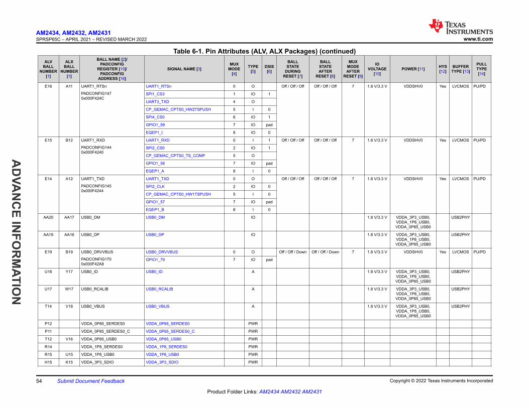
Table 6-1. Pin Attributes (ALV, ALX Packages) (continued)ALV
BALLNUMBER
[1]
ALX BALL
NUMBER [1]
BALL NAME [2]/PADCONFIG
REGISTER [15]/PADCONFIG
ADDRESS [16]
SIGNAL NAME [3]MUX
MODE [4]
TYPE [5]
DSIS [6]
BALLSTATE
DURINGRESET [7]
BALLSTATEAFTER
RESET [8]
MUXMODEAFTER
RESET [9]
IOVOLTAGE
[10]POWER [11] HYS
[12]BUFFER
TYPE [13]
PULLTYPE [14]
E16 A11 UART1_RTSn
PADCONFIG1470x000F424C
UART1_RTSn 0 O Off / Off / Off Off / Off / Off 7 1.8 V/3.3 V VDDSHV0 Yes LVCMOS PU/PD
SPI1_CS3 1 IO 1
UART3_TXD 4 O
CP_GEMAC_CPTS0_HW2TSPUSH 5 I 0
SPI4_CS0 6 IO 1
GPIO1_59 7 IO pad
EQEP1_I 8 IO 0
E15 B12 UART1_RXD
PADCONFIG1440x000F4240
UART1_RXD 0 I 1 Off / Off / Off Off / Off / Off 7 1.8 V/3.3 V VDDSHV0 Yes LVCMOS PU/PD
SPI2_CS0 2 IO 1
CP_GEMAC_CPTS0_TS_COMP 5 O
GPIO1_56 7 IO pad
EQEP1_A 8 I 0
E14 A12 UART1_TXD
PADCONFIG1450x000F4244
UART1_TXD 0 O Off / Off / Off Off / Off / Off 7 1.8 V/3.3 V VDDSHV0 Yes LVCMOS PU/PD
SPI2_CLK 2 IO 0
CP_GEMAC_CPTS0_HW1TSPUSH 5 I 0
GPIO1_57 7 IO pad
EQEP1_B 8 I 0
AA20 AA17 USB0_DM USB0_DM IO 1.8 V/3.3 V VDDA_3P3_USB0, VDDA_1P8_USB0, VDDA_0P85_USB0
USB2PHY
AA19 AA16 USB0_DP USB0_DP IO 1.8 V/3.3 V VDDA_3P3_USB0, VDDA_1P8_USB0, VDDA_0P85_USB0
USB2PHY
E19 B19 USB0_DRVVBUS
PADCONFIG1700x000F42A8
USB0_DRVVBUS 0 O Off / Off / Down Off / Off / Down 7 1.8 V/3.3 V VDDSHV0 Yes LVCMOS PU/PD
GPIO1_79 7 IO pad
U16 Y17 USB0_ID USB0_ID A 1.8 V/3.3 V VDDA_3P3_USB0, VDDA_1P8_USB0, VDDA_0P85_USB0
USB2PHY
U17 W17 USB0_RCALIB USB0_RCALIB A 1.8 V/3.3 V VDDA_3P3_USB0, VDDA_1P8_USB0, VDDA_0P85_USB0
USB2PHY
T14 V18 USB0_VBUS USB0_VBUS A 1.8 V/3.3 V VDDA_3P3_USB0, VDDA_1P8_USB0, VDDA_0P85_USB0
USB2PHY
P12 VDDA_0P85_SERDES0 VDDA_0P85_SERDES0 PWR
P11 VDDA_0P85_SERDES0_C VDDA_0P85_SERDES0_C PWR
T12 V16 VDDA_0P85_USB0 VDDA_0P85_USB0 PWR
R14 VDDA_1P8_SERDES0 VDDA_1P8_SERDES0 PWR
R15 U15 VDDA_1P8_USB0 VDDA_1P8_USB0 PWR
H15 K15 VDDA_3P3_SDIO VDDA_3P3_SDIO PWR
AM2434, AM2432, AM2431SPRSP65C – APRIL 2021 – REVISED MARCH 2022 www.ti.com
AD
VAN
CE IN
FOR
MATIO
N
54 Submit Document Feedback Copyright © 2022 Texas Instruments Incorporated
Product Folder Links: AM2434 AM2432 AM2431

Table 6-1. Pin Attributes (ALV, ALX Packages) (continued)ALV
BALLNUMBER
[1]
ALX BALL
NUMBER [1]
BALL NAME [2]/PADCONFIG
REGISTER [15]/PADCONFIG
ADDRESS [16]
SIGNAL NAME [3]MUX
MODE [4]
TYPE [5]
DSIS [6]
BALLSTATE
DURINGRESET [7]
BALLSTATEAFTER
RESET [8]
MUXMODEAFTER
RESET [9]
IOVOLTAGE
[10]POWER [11] HYS
[12]BUFFER
TYPE [13]
PULLTYPE [14]
R13 U16 VDDA_3P3_USB0 VDDA_3P3_USB0 PWR
J13 G17, H17 VDDA_ADC VDDA_ADC PWR
K12 H14 VDDA_MCU VDDA_MCU PWR
N12 N12 VDDA_PLL0 VDDA_PLL0 PWR
H9 G9 VDDA_PLL1 VDDA_PLL1 PWR
J11 G12 VDDA_PLL2 VDDA_PLL2 PWR
G11 G11 VDDA_TEMP0 VDDA_TEMP0 PWR
L11 M11 VDDA_TEMP1 VDDA_TEMP1 PWR
L10 G5, G6, J10, J12, P14, P8,
R10
VDDR_CORE VDDR_CORE PWR
F11 C13, D13, E14
VDDSHV0 VDDSHV0 PWR
M7 L6, M6, P5, P6
VDDSHV1 VDDSHV1 PWR
R8 T11, T8, U11, U7,
U8
VDDSHV2 VDDSHV2 PWR
P14 R17, T17 VDDSHV3 VDDSHV3 PWR
M14 N16, N17 VDDSHV4 VDDSHV4 PWR
L14 L16, L17 VDDSHV5 VDDSHV5 PWR
F9 E7, E8, E9
VDDSHV_MCU VDDSHV_MCU PWR
F7 VDDS_DDR VDDS_DDR PWR
J8 VDDS_DDR_C VDDS_DDR_C PWR
J15 VDDS_MMC0 VDDS_MMC0 PWR
H13 F18 VDDS_OSC VDDS_OSC PWR
J10 F11, G10, H15, H8, J9, K11,
K14, L13, L9, M14, M8, N10, N9, R12, R13, R9
VDD_CORE VDD_CORE PWR
H14 VDD_DLL_MMC0 VDD_DLL_MMC0 PWR
K13 VDD_MMC0 VDD_MMC0 PWR
K16 VMON_1P8_MCU VMON_1P8_MCU A
E12 F14 VMON_1P8_SOC VMON_1P8_SOC A
F13 VMON_3P3_MCU VMON_3P3_MCU A
F14 E15 VMON_3P3_SOC VMON_3P3_SOC A
K10 G13 VMON_VSYS VMON_VSYS A
www.ti.comAM2434, AM2432, AM2431
SPRSP65C – APRIL 2021 – REVISED MARCH 2022
AD
VAN
CE
INFO
RM
ATIO
N
Copyright © 2022 Texas Instruments Incorporated Submit Document Feedback 55
Product Folder Links: AM2434 AM2432 AM2431

Table 6-1. Pin Attributes (ALV, ALX Packages) (continued)ALV
BALLNUMBER
[1]
ALX BALL
NUMBER [1]
BALL NAME [2]/PADCONFIG
REGISTER [15]/PADCONFIG
ADDRESS [16]
SIGNAL NAME [3]MUX
MODE [4]
TYPE [5]
DSIS [6]
BALLSTATE
DURINGRESET [7]
BALLSTATEAFTER
RESET [8]
MUXMODEAFTER
RESET [9]
IOVOLTAGE
[10]POWER [11] HYS
[12]BUFFER
TYPE [13]
PULLTYPE [14]
G15 E16 VPP VPP PWR
A1, A21, AA1, AA15, AA18, AA21, C10,
C15, C3, D1, E11, E13, F10, F15, F8, G1, G16, G3, G7, G9, H11,
H20, H21, H6, H8, J14, J16, J7, J9, K6, K8, L1, L16, L3, L7, L9, M10,
M12, M6, M8, N11,
N13, N15, N7, N9, P1,
P10, P18, P6, P8,
R12, R7, R9, T10, T11, T15, T16, T8, U3, V17,
W10, W18,
Y14, Y17, Y19
A1, A2, A20, A21,
AA1, AA2, AA20, AA21,
B1, B21, D10, D16,
D17, E11, E13, E6, F17, F8,
G16, H16, H6, H7, J11, J16, J5, J6, K16, K6, K7, K8, L10, L11, L12,
M15, M16, M7, N11, N13, N6, P11,
P15, P16, P7, R11, R6, T14, U6, Y1,
Y21
VSS VSS GND
AM2434, AM2432, AM2431SPRSP65C – APRIL 2021 – REVISED MARCH 2022 www.ti.com
AD
VAN
CE IN
FOR
MATIO
N
56 Submit Document Feedback Copyright © 2022 Texas Instruments Incorporated
Product Folder Links: AM2434 AM2432 AM2431

6.3 Signal Descriptions
Many signals are available on multiple pins, according to the software configuration of the pin multiplexing options.
The following list describes the column headers:
1. SIGNAL NAME: The name of the signal passing through the pin.
Note
Signal names and descriptions provided in each Signal Descriptions table, represent the pin multiplexed signal function which is implemented at the pin and selected via PADCONFIG registers. Device subsystems may provide secondary multiplexing of signal functions, which are not described in these tables. For more information on secondary multiplexed signal functions, see the respective peripheral chapter of the device TRM.
2. PIN TYPE: Signal direction and type:Signal Type Description
I Input
O Output
IO Input, Output, or simultaneously Input and Output
IOD Input, Output, or simultaneously Input and Output, with open-drain output function
IOZ Input, Output, or simultaneously Input and Output, with three-state output function
OZ Output with three-state output function
A Analog
PWR Power
GND Ground
CAP LDO Capacitor
3. DESCRIPTION: Description of the signal4. BALL: Ball number(s) associated with signal
For more information on the I/O cell configurations, see the Pad Configuration Registers section within the Device Configuration chapter of the device TRM.
www.ti.comAM2434, AM2432, AM2431
SPRSP65C – APRIL 2021 – REVISED MARCH 2022
AD
VAN
CE
INFO
RM
ATIO
N
Copyright © 2022 Texas Instruments Incorporated Submit Document Feedback 57
Product Folder Links: AM2434 AM2432 AM2431

6.3.1 AM243x_ALX Package - Unsupported Interfaces and Signals
Note
The following signals are not supported by the AM243x_ALX device package. In some cases, the entire peripheral cannot be used due to critical interface signal unavailability.
Table 6-2. AM243x_ALX Package - Unsupported Peripheral Interfaces and Signals TableMAIN DOMAIN MCU DOMAIN
PERIPHERAL INSTANCES (1)
• DDRSS0*• EHRPWM4*• EHRPWM6*• FSI_TX1*• FSI_RX4*• FSI_RX5*• GPMC0*• I2C2*• MMC0*• SERDES0*• SPI1*
• MCU_I2C0*• MCU_I2C1*• MCU_SPI0*• MCU_SPI1*• MCU_UART1*
GPIO SIGNALS
• GPIO0_[7:10]• GPIO0_[13:14]• GPIO0_[31:35]• GPIO0_[37:44]• GPIO1_42• GPIO1_[47:51]• GPIO1_68• GPIO1_70
• MCU_GPIO[4:21]
MISCELLANEOUS SIGNALS
• CP_GEMAC_CPTS0_RFT_CLK• CPTS0_RFT_CLK• ECAP0_IN_APWM_OUT• EHRPWM5_B• EXTINTn• GPMC0_FCLK_MUX• OSPI0_D[4:7]• OSPI0_RESET_OUT[0:1]• OSPI0_CSn[2:3]• OSPI0_ECC_FAIL• PRG1_IEP0_EDIO_OUTVALID• SYNC0• TRACE[14:23]
• MCU_EXT_REFCLK0• MCU_SYSCLKOUT0• MCU_TIMER_IO[2:3]
(1) * dentotes the entire peripheral instance is not supported for the AM243x_ALX device package.
AM2434, AM2432, AM2431SPRSP65C – APRIL 2021 – REVISED MARCH 2022 www.ti.com
AD
VAN
CE IN
FOR
MATIO
N
58 Submit Document Feedback Copyright © 2022 Texas Instruments Incorporated
Product Folder Links: AM2434 AM2432 AM2431

6.3.2 ADCMAIN Domain Instances
Table 6-3. ADC0 Signal DescriptionsSignal Name [1] ((2)) Signal Type [2] Description [3] ALV PIN [4] ALX PIN [4]
ADC0_AIN0 (1) A ADC Analog Input 0 / GPIO1_80 (Input Only) G20 H21
ADC0_AIN1 (1) A ADC Analog Input 1 / GPIO1_81 (Input Only) F20 F19
ADC0_AIN2 (1) A ADC Analog Input 2 / GPIO1_82 (Input Only) E21 F21
ADC0_AIN3 (1) A ADC Analog Input 3 / GPIO1_83 (Input Only) D20 F20
ADC0_AIN4 (1) A ADC Analog Input 4 / GPIO1_84 (Input Only) G21 H20
ADC0_AIN5 (1) A ADC Analog Input 5 / GPIO1_85 (Input Only) F21 E21
ADC0_AIN6 (1) A ADC Analog Input 6 / GPIO1_86 (Input Only) F19 G20
ADC0_AIN7 (1) A ADC Analog Input 7 / GPIO1_87 (Input Only) E20 E20
ADC_EXT_TRIGGER0 I ADC Trigger Input B16, C13 B7, B9
ADC_EXT_TRIGGER1 I ADC Trigger Input D14, D16 C11
(1) Only digital input signals are supported when configured as GPIO.(2) The digital GPI functionality of these pins are controlled by the CTRLMMR_ADC0_CTRL[16] - GPI_MODE_EN register bit.
6.3.3 CPSWMAIN Domain Instances
Table 6-4. CPSW3G0 RGMII1 Signal DescriptionsSignal Name [1] Signal Type [2] Description [3] ALV PIN [4] ALX PIN [4]
RGMII1_RXC I RGMII Receive Clock AA5, W13 U1, Y13
RGMII1_RX_CTL I RGMII Receive Control V13, W6 U14, Y3
RGMII1_TXC IO RGMII Transmit Clock U14 W13
RGMII1_TX_CTL O RGMII Transmit Control U15 W16
RGMII1_RD0 I RGMII Receive Data 0 AA13, W5 AA11, T5
RGMII1_RD1 I RGMII Receive Data 1 U12, Y5 R2, W11
RGMII1_RD2 I RGMII Receive Data 2 V6, Y13 U2, Y15
RGMII1_RD3 I RGMII Receive Data 3 V12, V5 AA13, T1
RGMII1_TD0 O RGMII Transmit Data 0 V15 Y14
RGMII1_TD1 O RGMII Transmit Data 1 V14 Y16
RGMII1_TD2 O RGMII Transmit Data 2 W14 U13
RGMII1_TD3 O RGMII Transmit Data 3 AA14 AA14
Table 6-5. CPSW3G0 RGMII2 Signal DescriptionsSignal Name [1] Signal Type [2] Description [3] ALV PIN [4] ALX PIN [4]
RGMII2_RXC I RGMII Receive Clock U11 V10
RGMII2_RX_CTL I RGMII Receive Control W12 Y12
RGMII2_TXC IO RGMII Transmit Clock Y10 Y8
RGMII2_TX_CTL O RGMII Transmit Control Y11 V9
RGMII2_RD0 I RGMII Receive Data 0 W11 AA10
RGMII2_RD1 I RGMII Receive Data 1 V11 Y10
RGMII2_RD2 I RGMII Receive Data 2 AA12 Y11
RGMII2_RD3 I RGMII Receive Data 3 Y12 V12
RGMII2_TD0 O RGMII Transmit Data 0 AA10 Y6
RGMII2_TD1 O RGMII Transmit Data 1 V10 AA8
RGMII2_TD2 O RGMII Transmit Data 2 U10 Y9
RGMII2_TD3 O RGMII Transmit Data 3 AA11 W9
www.ti.comAM2434, AM2432, AM2431
SPRSP65C – APRIL 2021 – REVISED MARCH 2022
AD
VAN
CE
INFO
RM
ATIO
N
Copyright © 2022 Texas Instruments Incorporated Submit Document Feedback 59
Product Folder Links: AM2434 AM2432 AM2431

Table 6-6. CPSW3G0 RMII1 and RMII2 Signal DescriptionsSignal Name [1] Signal Type [2] Description [3] ALV PIN [4] ALX PIN [4]
RMII1_CRS_DV I RMII Carrier Sense / Data Valid R2, V12 AA13, F3
RMII1_RX_ER I RMII Receive Data Error U15, W6 W16, Y3
RMII1_TX_EN O RMII Transmit Enable P5, Y13 D1, Y15
RMII2_CRS_DV I RMII Carrier Sense / Data Valid U10 Y9
RMII2_RX_ER I RMII Receive Data Error W12 Y12
RMII2_TX_EN O RMII Transmit Enable Y11 V9
RMII1_RXD0 I RMII Receive Data 0 V15, W5 T5, Y14
RMII1_RXD1 I RMII Receive Data 1 V14, Y5 R2, Y16
RMII1_TXD0 O RMII Transmit Data 0 V6, W14 U13, U2
RMII1_TXD1 O RMII Transmit Data 1 AA14, V5 AA14, T1
RMII2_RXD0 I RMII Receive Data 0 W11 AA10
RMII2_RXD1 I RMII Receive Data 1 V11 Y10
RMII2_TXD0 O RMII Transmit Data 0 AA10 Y6
RMII2_TXD1 O RMII Transmit Data 1 V10 AA8
RMII_REF_CLK (1) I RMII Reference Clock AA5, U14 U1, W13
(1) RMII_REF_CLK is common to both RMII1 and RMII2.
6.3.3.1.1 CPSW3G IOSETs
Table 6-7 defines valid pin combinations of each CPSW3G MDIO0 IOSET.
Table 6-7. CPSW3G MDIO0 IOSETsSIGNALS IOSET1 IOSET2
BALL NAME MUXMODE BALL NAME MUXMODEMDIO0_MDIO PRG0_PRU1_GPO18 4 PRG1_MDIO0_MDIO 4
MDIO0_MDC PRG0_PRU1_GPO19 4 PRG1_MDIO0_MDC 4
Table 6-8 defines valid pin combinations of each CPSW3G RMII1 and RMII2 IOSET.
Table 6-8. CPSW3G RMII1 and RMII2 IOSETsSIGNALS IOSET1 IOSET2
BALL NAME MUXMODE BALL NAME MUXMODERMII_REF_CLK(1) PRG1_PRU0_GPO10 5 PRG0_PRU0_GPO10 5
RMII1_CRS_DV PRG1_PRU1_GPO19 5 PRG0_PRU1_GPO19 5
RMII1_RX_ER PRG1_PRU0_GPO9 5 PRG0_PRU0_GPO9 5
RMII1_RXD0 PRG1_PRU1_GPO7 5 PRG0_PRU1_GPO7 5
RMII1_RXD1 PRG1_PRU1_GPO9 5 PRG0_PRU1_GPO9 5
RMII1_TXD0 PRG1_PRU1_GPO10 5 PRG0_PRU1_GPO10 5
RMII1_TXD1 PRG1_PRU1_GPO17 5 PRG0_PRU1_GPO17 5
RMII1_TX_EN PRG1_PRU1_GPO18 5 PRG0_PRU1_GPO18 5
RMII2_CRS_DV PRG1_PRU1_GPO13 5 PRG1_PRU1_GPO13 5
RMII2_RX_ER PRG1_PRU1_GPO4 5 PRG1_PRU1_GPO4 5
RMII2_RXD0 PRG1_PRU1_GPO0 5 PRG1_PRU1_GPO0 5
RMII2_RXD1 PRG1_PRU1_GPO1 5 PRG1_PRU1_GPO1 5
RMII2_TXD0 PRG1_PRU1_GPO11 5 PRG1_PRU1_GPO11 5
RMII2_TXD1 PRG1_PRU1_GPO12 5 PRG1_PRU1_GPO12 5
RMII2_TX_EN PRG1_PRU1_GPO15 5 PRG1_PRU1_GPO15 5
(1) RMII_REF_CLK is common to both RMII1 and RMII2. For proper operation, all pin multiplexed signal assignments must use the same IOSET.
AM2434, AM2432, AM2431SPRSP65C – APRIL 2021 – REVISED MARCH 2022 www.ti.com
AD
VAN
CE IN
FOR
MATIO
N
60 Submit Document Feedback Copyright © 2022 Texas Instruments Incorporated
Product Folder Links: AM2434 AM2432 AM2431

Table 6-9 defines valid pin combinations of each CPSW3G RGMII1 IOSET.
Table 6-9. CPSW3G RGMII1 IOSETsSIGNALS IOSET1 IOSET2
BALL NAME MUXMODE BALL NAME MUXMODERGMII1_TX_CTL PRG1_PRU0_GPO9 4 PRG1_PRU0_GPO9 4
RGMII1_TXC PRG1_PRU0_GPO10 4 PRG1_PRU0_GPO10 4
RGMII1_TD0 PRG1_PRU1_GPO7 4 PRG1_PRU1_GPO7 4
RGMII1_TD1 PRG1_PRU1_GPO9 4 PRG1_PRU1_GPO9 4
RGMII1_TD2 PRG1_PRU1_GPO10 4 PRG1_PRU1_GPO10 4
RGMII1_TD3 PRG1_PRU1_GPO17 4 PRG1_PRU1_GPO17 4
RGMII1_RX_CTL PRG0_PRU0_GPO9 4 PRG1_PRU0_GPO5 4
RGMII1_RXC PRG0_PRU0_GPO10 4 PRG1_PRU0_GPO8 4
RGMII1_RD0 PRG0_PRU1_GPO7 4 PRG1_PRU1_GPO5 4
RGMII1_RD1 PRG0_PRU1_GPO9 4 PRG1_PRU1_GPO8 4
RGMII1_RD2 PRG0_PRU1_GPO10 4 PRG1_PRU1_GPO18 4
RGMII1_RD3 PRG0_PRU1_GPO17 4 PRG1_PRU1_GPO19 4
6.3.4 CPTSMAIN Domain Instances
Table 6-10. CP GEMAC CPTS0 Signal DescriptionsSignal Name [1] Signal Type [2] Description [3] ALV PIN [4] ALX PIN [4]
CP_GEMAC_CPTS0_RFT_CLK (1) I CPTS Reference Clock Input to CPSW3G0 CPTS D18
CP_GEMAC_CPTS0_TS_COMP O CPTS Time Stamp Counter Compare Output from CPSW3G0 CPTS E15, K18, W1 B12, G2, K18
CP_GEMAC_CPTS0_TS_SYNC O CPTS Time Stamp Counter Bit Output from CPSW3G0 CPTS B16, D16, K19, U1 B9, C11, E1, K20
CP_GEMAC_CPTS0_HW1TSPUSH I CPTS Hardware Time Stamp Push Input to CPSW3G0
CPTS E14, L21, V1 A12, J19, K4
CP_GEMAC_CPTS0_HW2TSPUSH I CPTS Hardware Time Stamp Push Input to CPSW3G0
CPTS E16, K21, T1 A11, E2, J18
(1) The CP_GEMAC_CPTS0_RFT_CLK signal is not supported by the AM243x_ALX device package. See AM243x_ALX Package - Unsupported Interfaces and Signals for additional details.
Table 6-11. CPTS0 Signal DescriptionsSignal Name [1] Signal Type [2] Description [3] ALV PIN [4] ALX PIN [4]
CPTS0_RFT_CLK (2) I CPTS Reference Clock Input D18
CPTS0_TS_COMP O CPTS Time Stamp Counter Compare Output C13, W1, W7 B7, G2, U3
CPTS0_TS_SYNC O CPTS Time Stamp Counter Bit Output D14, U1, U7 E1, T2
CPTS0_HW1TSPUSH I CPTS Hardware Time Stamp Push Input to Time Sync Router C18, V1, V7 A17, K4, Y4
CPTS0_HW2TSPUSH I CPTS Hardware Time Stamp Push Input to Time Sync Router B19, T1, U13 B18, E2, V13
SYNC0_OUT (1) O CPTS Time Stamp Generator Bit 0 Output from Time Sync Router D18
SYNC1_OUT O CPTS Time Stamp Generator Bit 1 Output from Time Sync Router A19 A18
SYNC2_OUT O CPTS Time Stamp Generator Bit 2 Output from Time Sync Router A17 B13
SYNC3_OUT O CPTS Time Stamp Generator Bit 3 Output from Time Sync Router B17 A14
(1) The SYNC0_OUT signal is not supported by the AM243x_ALX device package. See AM243x_ALX Package - Unsupported Interfaces and Signals for additional details.
(2) The CPTS0_RFT_CLK signal is not supported by the AM243x_ALX device package. See AM243x_ALX Package - Unsupported Interfaces and Signals for additional details.
www.ti.comAM2434, AM2432, AM2431
SPRSP65C – APRIL 2021 – REVISED MARCH 2022
AD
VAN
CE
INFO
RM
ATIO
N
Copyright © 2022 Texas Instruments Incorporated Submit Document Feedback 61
Product Folder Links: AM2434 AM2432 AM2431

6.3.5 DDRSSMAIN Domain Instances
Table 6-12. DDRSS0 Signal DescriptionsSignal Name [1] ((1)) Signal Type [2] Description [3] ALV PIN [4] ALX PIN [4]
DDR0_ACT_n O DDRSS Activation Command H2
DDR0_ALERT_n IO DDRSS Alert H1
DDR0_CAS_n O DDRSS Column Address Strobe J5
DDR0_PAR O DDRSS Command and Address Parity K5
DDR0_RAS_n O DDRSS Row Address Strobe F6
DDR0_WE_n O DDRSS Write Enable H4
DDR0_A0 O DDRSS Address Bus D2
DDR0_A1 O DDRSS Address Bus C5
DDR0_A2 O DDRSS Address Bus E2
DDR0_A3 O DDRSS Address Bus D4
DDR0_A4 O DDRSS Address Bus D3
DDR0_A5 O DDRSS Address Bus F2
DDR0_A6 O DDRSS Address Bus J2
DDR0_A7 O DDRSS Address Bus L5
DDR0_A8 O DDRSS Address Bus J3
DDR0_A9 O DDRSS Address Bus J4
DDR0_A10 O DDRSS Address Bus K3
DDR0_A11 O DDRSS Address Bus J1
DDR0_A12 O DDRSS Address Bus M5
DDR0_A13 O DDRSS Address Bus K4
DDR0_BA0 O DDRSS Bank Address G4
DDR0_BA1 O DDRSS Bank Address G5
DDR0_BG0 O DDRSS Bank Group G2
DDR0_BG1 O DDRSS Bank Group H3
DDR0_CAL0 A IO Pad Calibration Resistor H5
DDR0_CK0 O DDRSS Clock F1
DDR0_CK0_n O DDRSS Negative Clock E1
DDR0_CKE0 O DDRSS Clock Enable F4
DDR0_CKE1 O DDRSS Clock Enable F3
DDR0_CS0_n O DDRSS Chip Select 0 E3
DDR0_CS1_n O DDRSS Chip Select 1 E4
DDR0_DM0 IO DDRSS Data Mask B2
DDR0_DM1 IO DDRSS Data Mask M2
DDR0_DQ0 IO DDRSS Data A3
DDR0_DQ1 IO DDRSS Data A2
DDR0_DQ2 IO DDRSS Data B5
DDR0_DQ3 IO DDRSS Data A4
DDR0_DQ4 IO DDRSS Data B3
DDR0_DQ5 IO DDRSS Data C4
DDR0_DQ6 IO DDRSS Data C2
DDR0_DQ7 IO DDRSS Data B4
DDR0_DQ8 IO DDRSS Data N5
DDR0_DQ9 IO DDRSS Data L4
DDR0_DQ10 IO DDRSS Data L2
DDR0_DQ11 IO DDRSS Data M3
DDR0_DQ12 IO DDRSS Data N4
DDR0_DQ13 IO DDRSS Data N3
AM2434, AM2432, AM2431SPRSP65C – APRIL 2021 – REVISED MARCH 2022 www.ti.com
AD
VAN
CE IN
FOR
MATIO
N
62 Submit Document Feedback Copyright © 2022 Texas Instruments Incorporated
Product Folder Links: AM2434 AM2432 AM2431
Table 6-12. DDRSS0 Signal Descriptions (continued)Signal Name [1] ((1)) Signal Type [2] Description [3] ALV PIN [4] ALX PIN [4]
DDR0_DQ14 IO DDRSS Data M4
DDR0_DQ15 IO DDRSS Data N2
DDR0_DQS0 IO DDRSS Data Strobe 0 C1
DDR0_DQS0_n IO DDRSS Complimentary Data Strobe 0 B1
DDR0_DQS1 IO DDRSS Data Strobe 1 N1
DDR0_DQS1_n IO DDRSS Complimentary Data Strobe 1 M1
DDR0_ODT0 O DDRSS On-Die Termination for Chip Select 0 E5
DDR0_ODT1 O DDRSS On-Die Termination for Chip Select 1 F5
DDR0_RESET0_n O DDRSS Reset D5
(1) The DDRSS0 interface is not supported by the AM243x_ALX device package. See AM243x_ALX Package - Unsupported Interfaces and Signals for additional details.
6.3.6 ECAPMAIN Domain Instances
Table 6-13. ECAP0 Signal DescriptionsSignal Name [1] Signal Type [2] Description [3] ALV PIN [4] ALX PIN [4]
ECAP0_IN_APWM_OUT (1) IO Enhanced Capture (ECAP) Input or Auxiliary PWM (APWM) Ouput D18
(1) The ECAP0_IN_APWM_OUT signal is not supported by the AM243x_ALX device package. See AM243x_ALX Package - Unsupported Interfaces and Signals for additional details.
Table 6-14. ECAP1 Signal DescriptionsSignal Name [1] Signal Type [2] Description [3] ALV PIN [4] ALX PIN [4]
ECAP1_IN_APWM_OUT IO Enhanced Capture (ECAP) Input or Auxiliary PWM (APWM) Ouput C17 B14
Table 6-15. ECAP2 Signal DescriptionsSignal Name [1] Signal Type [2] Description [3] ALV PIN [4] ALX PIN [4]
ECAP2_IN_APWM_OUT IO Enhanced Capture (ECAP) Input or Auxiliary PWM (APWM) Ouput D17 A15
6.3.7 Emulation and DebugMAIN Domain Instances
Table 6-16. Trace Signal DescriptionsSignal Name [1] Signal Type [2] Description [3] ALV PIN [4] ALX PIN [4]
TRC_CLK O Trace Clock T20 R21
TRC_CTL O Trace Control U21 R20
TRC_DATA0 O Trace Data 0 T18 T19
TRC_DATA1 O Trace Data 1 U20 V21
TRC_DATA2 O Trace Data 2 U18 U21
TRC_DATA3 O Trace Data 3 U19 T20
TRC_DATA4 O Trace Data 4 V20 T18
TRC_DATA5 O Trace Data 5 V21 U19
TRC_DATA6 O Trace Data 6 V19 U18
TRC_DATA7 O Trace Data 7 T17 U20
TRC_DATA8 O Trace Data 8 R16 V20
TRC_DATA9 O Trace Data 9 W20 W20
TRC_DATA10 O Trace Data 10 W21 Y20
TRC_DATA11 O Trace Data 11 V18 Y19
TRC_DATA12 O Trace Data 12 Y21 Y18
www.ti.comAM2434, AM2432, AM2431
SPRSP65C – APRIL 2021 – REVISED MARCH 2022
AD
VAN
CE
INFO
RM
ATIO
N
Copyright © 2022 Texas Instruments Incorporated Submit Document Feedback 63
Product Folder Links: AM2434 AM2432 AM2431

Table 6-16. Trace Signal Descriptions (continued)Signal Name [1] Signal Type [2] Description [3] ALV PIN [4] ALX PIN [4]
TRC_DATA13 O Trace Data 13 Y20 AA19
TRC_DATA14 (1) O Trace Data 14 R17
TRC_DATA15 (1) O Trace Data 15 P16
TRC_DATA16 (1) O Trace Data 16 R18
TRC_DATA17 (1) O Trace Data 17 T21
TRC_DATA18 (1) O Trace Data 18 P17
TRC_DATA19 (1) O Trace Data 19 T19 P21
TRC_DATA20 (1) O Trace Data 20 W19
TRC_DATA21 (1) O Trace Data 21 Y18
TRC_DATA22 (1) O Trace Data 22 N16
TRC_DATA23 (1) O Trace Data 23 R19
(1) This TRC_DATA signal is not supported by the AM243x_ALX device package. See AM243x_ALX Package - Unsupported Interfaces and Signals for additional details.
MCU Domain Instances
Table 6-17. JTAG Signal DescriptionsSignal Name [1] Signal Type [2] Description [3] ALV PIN [4] ALX PIN [4]
EMU0 IO Emulation Control 0 D10 C5
EMU1 IO Emulation Control 1 E10 B3
TCK I JTAG Test Clock Input B11 C6
TDI I JTAG Test Data Input C11 A3
TDO OZ JTAG Test Data Output A12 B5
TMS I JTAG Test Mode Select Input C12 B4
TRSTn I JTAG Reset D11 B6
6.3.8 EPWMMAIN Domain Instances
Table 6-18. EPWM Signal DescriptionsSignal Name [1] Signal Type [2] Description [3] ALV PIN [4] ALX PIN [4]
EHRPWM_SOCA O EHRPWM Start of Conversion A C17 B14
EHRPWM_SOCB O EHRPWM Start of Conversion B D17 A15
EHRPWM_TZn_IN0 I EHRPWM Trip Zone Input 0 (active low) T18 T19
EHRPWM_TZn_IN1 I EHRPWM Trip Zone Input 1 (active low) V21 U19
EHRPWM_TZn_IN2 I EHRPWM Trip Zone Input 2 (active low) R16, R20 V20
EHRPWM_TZn_IN3 (1) I EHRPWM Trip Zone Input 3 (active low) P16
EHRPWM_TZn_IN4 (2) I EHRPWM Trip Zone Input 4 (active low) P17, P19
EHRPWM_TZn_IN5 (3) I EHRPWM Trip Zone Input 5 (active low) R21, Y18
(1) The EHRPWM_TZn_IN3 signal is not supported by the AM243x_ALX device package. See AM243x_ALX Package - Unsupported Interfaces and Signals for additional details.
(2) The EHRPWM_TZn_IN4 signal is not supported by the AM243x_ALX device package. See AM243x_ALX Package - Unsupported Interfaces and Signals for additional details.
(3) The EHRPWM_TZn_IN5 signal is not supported by the AM243x_ALX device package. See AM243x_ALX Package - Unsupported Interfaces and Signals for additional details.
Table 6-19. EPWM0 Signal DescriptionsSignal Name [1] Signal Type [2] Description [3] ALV PIN [4] ALX PIN [4]
EHRPWM0_A IO EHRPWM Output A U20 V21
EHRPWM0_B IO EHRPWM Output B U18 U21
EHRPWM0_SYNCI I Sync Input to EHRPWM module from an external pin T20 R21
EHRPWM0_SYNCO O Sync Output to EHRPWM module to an external pin U21 R20
AM2434, AM2432, AM2431SPRSP65C – APRIL 2021 – REVISED MARCH 2022 www.ti.com
AD
VAN
CE IN
FOR
MATIO
N
64 Submit Document Feedback Copyright © 2022 Texas Instruments Incorporated
Product Folder Links: AM2434 AM2432 AM2431

Table 6-20. EPWM1 Signal DescriptionsSignal Name [1] Signal Type [2] Description [3] ALV PIN [4] ALX PIN [4]
EHRPWM1_A IO EHRPWM Output A U19 T20
EHRPWM1_B IO EHRPWM Output B V20 T18
Table 6-21. EPWM2 Signal DescriptionsSignal Name [1] Signal Type [2] Description [3] ALV PIN [4] ALX PIN [4]
EHRPWM2_A IO EHRPWM Output A V19 U18
EHRPWM2_B IO EHRPWM Output B T17 U20
Table 6-22. EPWM3 Signal DescriptionsSignal Name [1] Signal Type [2] Description [3] ALV PIN [4] ALX PIN [4]
EHRPWM3_A IO EHRPWM Output A V18 Y19
EHRPWM3_B IO EHRPWM Output B Y21 Y18
EHRPWM3_SYNCI I Sync Input to EHRPWM module from an external pin Y20 AA19
EHRPWM3_SYNCO (1) O Sync Output to EHRPWM module to an external pin R17
(1) The EHRPWM3_SYNCO signal is not supported by the AM243x_ALX device package. See AM243x_ALX Package - Unsupported Interfaces and Signals for additional details.
Table 6-23. EPWM4 Signal DescriptionsSignal Name [1] ((1)) Signal Type [2] Description [3] ALV PIN [4] ALX PIN [4]
EHRPWM4_A IO EHRPWM Output A R18
EHRPWM4_B IO EHRPWM Output B T21
(1) The EPWM4 interface is not supported by the AM243x_ALX device package. See AM243x_ALX Package - Unsupported Interfaces and Signals for additional details.
Table 6-24. EPWM5 Signal DescriptionsSignal Name [1] Signal Type [2] Description [3] ALV PIN [4] ALX PIN [4]
EHRPWM5_A IO EHRPWM Output A T19 P21
EHRPWM5_B (1) IO EHRPWM Output B W19
(1) The EHRPWM5_B signal is not supported by the AM243x_ALX device package. See AM243x_ALX Package - Unsupported Interfaces and Signals for additional details.
Table 6-25. EPWM6 Signal DescriptionsSignal Name [1] ((1)) Signal Type [2] Description [3] ALV PIN [4] ALX PIN [4]
EHRPWM6_A IO EHRPWM Output A B14, N16
EHRPWM6_B IO EHRPWM Output B A15, N17
EHRPWM6_SYNCI I Sync Input to EHRPWM module from an external pin C14, R19
EHRPWM6_SYNCO O Sync Output to EHRPWM module to an external pin B15, R20
(1) The EPWM6 interface is not supported by the AM243x_ALX device package. See AM243x_ALX Package - Unsupported Interfaces and Signals for additional details.
Table 6-26. EPWM7 Signal DescriptionsSignal Name [1] Signal Type [2] Description [3] ALV PIN [4] ALX PIN [4]
EHRPWM7_A IO EHRPWM Output A P17, P5, W20 D1, W20
EHRPWM7_B IO EHRPWM Output B R2, W21, Y18 F3, Y20
Table 6-27. EPWM8 Signal DescriptionsSignal Name [1] Signal Type [2] Description [3] ALV PIN [4] ALX PIN [4]
EHRPWM8_A IO EHRPWM Output A V1, V21 K4, U19
EHRPWM8_B IO EHRPWM Output B R16, W1 G2, V20
www.ti.comAM2434, AM2432, AM2431
SPRSP65C – APRIL 2021 – REVISED MARCH 2022
AD
VAN
CE
INFO
RM
ATIO
N
Copyright © 2022 Texas Instruments Incorporated Submit Document Feedback 65
Product Folder Links: AM2434 AM2432 AM2431

6.3.9 EQEPMAIN Domain Instances
Table 6-28. EQEP0 Signal DescriptionsSignal Name [1] Signal Type [2] Description [3] ALV PIN [4] ALX PIN [4]
EQEP0_A I EQEP Quadrature Input A D15, N16, Y2 B10, L5
EQEP0_B I EQEP Quadrature Input B C16, N17, W2 B11, J2
EQEP0_I IO EQEP Index A16, R20, T6, Y5 A9, R2, T4
EQEP0_S IO EQEP Strobe B16, R19, V3 B9, M2
Table 6-29. EQEP1 Signal DescriptionsSignal Name [1] Signal Type [2] Description [3] ALV PIN [4] ALX PIN [4]
EQEP1_A I EQEP Quadrature Input A E15, T4, W20 B12, L2, W20
EQEP1_B I EQEP Quadrature Input B E14, W21, W3 A12, L3, Y20
EQEP1_I IO EQEP Index E16, R21, U6, V6 A11, R5, U2
EQEP1_S IO EQEP Strobe D16, P19, P4 C11, E3
Table 6-30. EQEP2 Signal DescriptionsSignal Name [1] Signal Type [2] Description [3] ALV PIN [4] ALX PIN [4]
EQEP2_A I EQEP Quadrature Input A C17, R5 B14, F5
EQEP2_B I EQEP Quadrature Input B D17, W5, Y4 A15, P2, T5
EQEP2_I IO EQEP Index A17, W4 B13, P1
EQEP2_S IO EQEP Strobe B17, R1 A14, F4
6.3.10 FSIMAIN Domain Instances
Table 6-31. FSI0 RX Signal DescriptionsSignal Name [1] Signal Type [2] Description [3] ALV PIN [4] ALX PIN [4]
FSI_RX0_CLK I FSI Reciever Clock V19 U18
FSI_RX0_D0 I FSI Receiver Data 0 T17 U20
FSI_RX0_D1 I FSI Receiver Data 1 R16 V20
Table 6-32. FSI0 TX Signal DescriptionsSignal Name [1] Signal Type [2] Description [3] ALV PIN [4] ALX PIN [4]
FSI_TX0_CLK O FSI Transmit Clock T19 P21
FSI_TX0_D0 O FSI Transmit Data 0 Y21 Y18
FSI_TX0_D1 O FSI Transmit Data 1 Y20 AA19
Table 6-33. FSI1 RX Signal DescriptionsSignal Name [1] Signal Type [2] Description [3] ALV PIN [4] ALX PIN [4]
FSI_RX1_CLK I FSI Reciever Clock W20 W20
FSI_RX1_D0 I FSI Receiver Data 0 W21 Y20
FSI_RX1_D1 I FSI Receiver Data 1 V18 Y19
Table 6-34. FSI1 TX Signal DescriptionsSignal Name [1] ((1)) Signal Type [2] Description [3] ALV PIN [4] ALX PIN [4]
FSI_TX1_CLK O FSI Transmit Clock N16
FSI_TX1_D0 O FSI Transmit Data 0 P17
FSI_TX1_D1 O FSI Transmit Data 1 Y18
(1) The FSI1 TX interface is not supported by the AM243x_ALX device package. See AM243x_ALX Package - Unsupported Interfaces and Signals for additional details.
AM2434, AM2432, AM2431SPRSP65C – APRIL 2021 – REVISED MARCH 2022 www.ti.com
AD
VAN
CE IN
FOR
MATIO
N
66 Submit Document Feedback Copyright © 2022 Texas Instruments Incorporated
Product Folder Links: AM2434 AM2432 AM2431

Table 6-35. FSI2 RX Signal DescriptionsSignal Name [1] Signal Type [2] Description [3] ALV PIN [4] ALX PIN [4]
FSI_RX2_CLK I FSI Reciever Clock T20 R21
FSI_RX2_D0 I FSI Receiver Data 0 U21 R20
FSI_RX2_D1 I FSI Receiver Data 1 T18 T19
Table 6-36. FSI3 RX Signal DescriptionsSignal Name [1] Signal Type [2] Description [3] ALV PIN [4] ALX PIN [4]
FSI_RX3_CLK I FSI Reciever Clock U20 V21
FSI_RX3_D0 I FSI Receiver Data 0 U18 U21
FSI_RX3_D1 I FSI Receiver Data 1 U19 T20
Table 6-37. FSI4 RX Signal DescriptionsSignal Name [1] ((1)) Signal Type [2] Description [3] ALV PIN [4] ALX PIN [4]
FSI_RX4_CLK I FSI Reciever Clock R17
FSI_RX4_D0 I FSI Receiver Data 0 V20 T18
FSI_RX4_D1 I FSI Receiver Data 1 V21 U19
(1) The FSI4 RX interface is not supported by the AM243x_ALX device package. See AM243x_ALX Package - Unsupported Interfaces and Signals for additional details.
Table 6-38. FSI5 RX Signal DescriptionsSignal Name [1] ((1)) Signal Type [2] Description [3] ALV PIN [4] ALX PIN [4]
FSI_RX5_CLK I FSI Reciever Clock P16
FSI_RX5_D0 I FSI Receiver Data 0 R18
FSI_RX5_D1 I FSI Receiver Data 1 T21
(1) The FSI5 RX interface is not supported by the AM243x_ALX device package. See AM243x_ALX Package - Unsupported Interfaces and Signals for additional details.
6.3.11 GPIOMAIN Domain Instances
Table 6-39. GPIO0 Signal DescriptionsSignal Name [1] Signal Type [2] Description [3] ALV PIN [4] ALX PIN [4]
GPIO0_0 IO General Purpose Input/Output N20 P20
GPIO0_1 IO General Purpose Input/Output N21 M21
GPIO0_2 IO General Purpose Input/Output N19 P17
GPIO0_3 IO General Purpose Input/Output M19 L19
GPIO0_4 IO General Purpose Input/Output M18 N20
GPIO0_5 IO General Purpose Input/Output M20 L21
GPIO0_6 IO General Purpose Input/Output M21 N19
GPIO0_7 (1) IO General Purpose Input/Output P21
GPIO0_8 (1) IO General Purpose Input/Output P20
GPIO0_9 (1) IO General Purpose Input/Output N18
GPIO0_10 (1) IO General Purpose Input/Output M17
GPIO0_11 IO General Purpose Input/Output L19 L20
GPIO0_12 IO General Purpose Input/Output L18 M20
GPIO0_13 (1) IO General Purpose Input/Output K17
GPIO0_14 (1) IO General Purpose Input/Output L17
GPIO0_15 IO General Purpose Input/Output T20 R21
GPIO0_16 IO General Purpose Input/Output U21 R20
GPIO0_17 IO General Purpose Input/Output T18 T19
GPIO0_18 IO General Purpose Input/Output U20 V21
GPIO0_19 IO General Purpose Input/Output AA14 AA14
www.ti.comAM2434, AM2432, AM2431
SPRSP65C – APRIL 2021 – REVISED MARCH 2022
AD
VAN
CE
INFO
RM
ATIO
N
Copyright © 2022 Texas Instruments Incorporated Submit Document Feedback 67
Product Folder Links: AM2434 AM2432 AM2431

Table 6-39. GPIO0 Signal Descriptions (continued)Signal Name [1] Signal Type [2] Description [3] ALV PIN [4] ALX PIN [4]
GPIO0_20 IO General Purpose Input/Output Y13 Y15
GPIO0_21 IO General Purpose Input/Output V20 T18
GPIO0_22 IO General Purpose Input/Output V21 U19
GPIO0_23 IO General Purpose Input/Output V19 U18
GPIO0_24 IO General Purpose Input/Output T17 U20
GPIO0_25 IO General Purpose Input/Output R16 V20
GPIO0_26 IO General Purpose Input/Output W20 W20
GPIO0_27 IO General Purpose Input/Output W21 Y20
GPIO0_28 IO General Purpose Input/Output V18 Y19
GPIO0_29 IO General Purpose Input/Output Y21 Y18
GPIO0_30 IO General Purpose Input/Output Y20 AA19
GPIO0_31 (1) IO General Purpose Input/Output R17
GPIO0_32 (1) IO General Purpose Input/Output P16
GPIO0_33 (1) IO General Purpose Input/Output R18
GPIO0_34 (1) IO General Purpose Input/Output T21
GPIO0_35 (1) IO General Purpose Input/Output P17
GPIO0_36 IO General Purpose Input/Output T19 P21
GPIO0_37 (1) IO General Purpose Input/Output W19
GPIO0_38 (1) IO General Purpose Input/Output Y18
GPIO0_39 (1) IO General Purpose Input/Output N16
GPIO0_40 (1) IO General Purpose Input/Output N17
GPIO0_41 (1) IO General Purpose Input/Output R19
GPIO0_42 (1) IO General Purpose Input/Output R20
GPIO0_43 (1) IO General Purpose Input/Output P19
GPIO0_44 (1) IO General Purpose Input/Output R21
GPIO0_45 IO General Purpose Input/Output Y7 V4
GPIO0_46 IO General Purpose Input/Output U8 W5
GPIO0_47 IO General Purpose Input/Output W8 AA4
GPIO0_48 IO General Purpose Input/Output V8 Y5
GPIO0_49 IO General Purpose Input/Output Y8 AA5
GPIO0_50 IO General Purpose Input/Output V13 U14
GPIO0_51 IO General Purpose Input/Output AA7 Y2
GPIO0_52 IO General Purpose Input/Output U13 V13
GPIO0_53 IO General Purpose Input/Output W13 Y13
GPIO0_54 IO General Purpose Input/Output U15 W16
GPIO0_55 IO General Purpose Input/Output U14 W13
GPIO0_56 IO General Purpose Input/Output AA8 V5
GPIO0_57 IO General Purpose Input/Output U9 W2
GPIO0_58 IO General Purpose Input/Output W9 V6
GPIO0_59 IO General Purpose Input/Output AA9 AA7
GPIO0_60 IO General Purpose Input/Output Y9 Y7
GPIO0_61 IO General Purpose Input/Output V9 W6
GPIO0_62 IO General Purpose Input/Output U7 T2
GPIO0_63 IO General Purpose Input/Output V7 Y4
GPIO0_64 IO General Purpose Input/Output W7 U3
GPIO0_65 IO General Purpose Input/Output W11 AA10
GPIO0_66 IO General Purpose Input/Output V11 Y10
GPIO0_67 IO General Purpose Input/Output AA12 Y11
GPIO0_68 IO General Purpose Input/Output Y12 V12
GPIO0_69 IO General Purpose Input/Output W12 Y12
AM2434, AM2432, AM2431SPRSP65C – APRIL 2021 – REVISED MARCH 2022 www.ti.com
AD
VAN
CE IN
FOR
MATIO
N
68 Submit Document Feedback Copyright © 2022 Texas Instruments Incorporated
Product Folder Links: AM2434 AM2432 AM2431

Table 6-39. GPIO0 Signal Descriptions (continued)Signal Name [1] Signal Type [2] Description [3] ALV PIN [4] ALX PIN [4]
GPIO0_70 IO General Purpose Input/Output AA13 AA11
GPIO0_71 IO General Purpose Input/Output U11 V10
GPIO0_72 IO General Purpose Input/Output V15 Y14
GPIO0_73 IO General Purpose Input/Output U12 W11
GPIO0_74 IO General Purpose Input/Output V14 Y16
GPIO0_75 IO General Purpose Input/Output W14 U13
GPIO0_76 IO General Purpose Input/Output AA10 Y6
GPIO0_77 IO General Purpose Input/Output V10 AA8
GPIO0_78 IO General Purpose Input/Output U10 Y9
GPIO0_79 IO General Purpose Input/Output AA11 W9
GPIO0_80 IO General Purpose Input/Output Y11 V9
GPIO0_81 IO General Purpose Input/Output Y10 Y8
GPIO0_82 IO General Purpose Input/Output U18 U21
GPIO0_83 IO General Purpose Input/Output U19 T20
GPIO0_84 IO General Purpose Input/Output V12 AA13
GPIO0_85 IO General Purpose Input/Output AA6 V2
GPIO0_86 IO General Purpose Input/Output Y6 W1
(1) This GPIO0 signal is not supported by the AM243x_ALX device package. See AM243x_ALX Package - Unsupported Interfaces and Signals for additional details.
Table 6-40. GPIO1 Signal DescriptionsSignal Name [1] Signal Type [2] Description [3] ALV PIN [4] ALX PIN [4]
GPIO1_0 IO General Purpose Input/Output Y1 J3
GPIO1_1 IO General Purpose Input/Output R4 J4
GPIO1_2 IO General Purpose Input/Output U2 G1
GPIO1_3 IO General Purpose Input/Output V2 H1
GPIO1_4 IO General Purpose Input/Output AA2 K2
GPIO1_5 IO General Purpose Input/Output R3 F2
GPIO1_6 IO General Purpose Input/Output T3 H2
GPIO1_7 IO General Purpose Input/Output T1 E2
GPIO1_8 IO General Purpose Input/Output T2 H5
GPIO1_9 IO General Purpose Input/Output W6 Y3
GPIO1_10 IO General Purpose Input/Output AA5 U1
GPIO1_11 IO General Purpose Input/Output Y3 L1
GPIO1_12 IO General Purpose Input/Output AA3 K1
GPIO1_13 IO General Purpose Input/Output R6 N1
GPIO1_14 IO General Purpose Input/Output V4 N2
GPIO1_15 IO General Purpose Input/Output T5 N4
GPIO1_16 IO General Purpose Input/Output U4 N3
GPIO1_17 IO General Purpose Input/Output U1 E1
GPIO1_18 IO General Purpose Input/Output V1 K4
GPIO1_19 IO General Purpose Input/Output W1 G2
GPIO1_20 IO General Purpose Input/Output Y2 L5
GPIO1_21 IO General Purpose Input/Output W2 J2
GPIO1_22 IO General Purpose Input/Output V3 M2
GPIO1_23 IO General Purpose Input/Output T4 L2
GPIO1_24 IO General Purpose Input/Output W3 L3
GPIO1_25 IO General Purpose Input/Output P4 E3
GPIO1_26 IO General Purpose Input/Output R5 F5
GPIO1_27 IO General Purpose Input/Output W5 T5
www.ti.comAM2434, AM2432, AM2431
SPRSP65C – APRIL 2021 – REVISED MARCH 2022
AD
VAN
CE
INFO
RM
ATIO
N
Copyright © 2022 Texas Instruments Incorporated Submit Document Feedback 69
Product Folder Links: AM2434 AM2432 AM2431

Table 6-40. GPIO1 Signal Descriptions (continued)Signal Name [1] Signal Type [2] Description [3] ALV PIN [4] ALX PIN [4]
GPIO1_28 IO General Purpose Input/Output R1 F4
GPIO1_29 IO General Purpose Input/Output Y5 R2
GPIO1_30 IO General Purpose Input/Output V6 U2
GPIO1_31 IO General Purpose Input/Output W4 P1
GPIO1_32 IO General Purpose Input/Output Y4 P2
GPIO1_33 IO General Purpose Input/Output T6 T4
GPIO1_34 IO General Purpose Input/Output U6 R5
GPIO1_35 IO General Purpose Input/Output U5 M4
GPIO1_36 IO General Purpose Input/Output AA4 T3
GPIO1_37 IO General Purpose Input/Output V5 T1
GPIO1_38 IO General Purpose Input/Output P5 D1
GPIO1_39 IO General Purpose Input/Output R2 F3
GPIO1_40 IO General Purpose Input/Output P2 E4
GPIO1_41 IO General Purpose Input/Output P3 D2
GPIO1_42 (1) IO General Purpose Input/Output D12
GPIO1_43 IO General Purpose Input/Output C13 B7
GPIO1_44 IO General Purpose Input/Output D13 B8
GPIO1_45 IO General Purpose Input/Output A13 A8
GPIO1_46 IO General Purpose Input/Output A14 C9
GPIO1_47 (1) IO General Purpose Input/Output B14
GPIO1_48 (1) IO General Purpose Input/Output D14
GPIO1_49 (1) IO General Purpose Input/Output C14
GPIO1_50 (1) IO General Purpose Input/Output B15
GPIO1_51 (1) IO General Purpose Input/Output A15
GPIO1_52 IO General Purpose Input/Output D15 B10
GPIO1_53 IO General Purpose Input/Output C16 B11
GPIO1_54 IO General Purpose Input/Output B16 B9
GPIO1_55 IO General Purpose Input/Output A16 A9
GPIO1_56 IO General Purpose Input/Output E15 B12
GPIO1_57 IO General Purpose Input/Output E14 A12
GPIO1_58 IO General Purpose Input/Output D16 C11
GPIO1_59 IO General Purpose Input/Output E16 A11
GPIO1_60 IO General Purpose Input/Output A17 B13
GPIO1_61 IO General Purpose Input/Output B17 A14
GPIO1_62 IO General Purpose Input/Output C17 B14
GPIO1_63 IO General Purpose Input/Output D17 A15
GPIO1_64 IO General Purpose Input/Output A18 B16
GPIO1_65 IO General Purpose Input/Output B18 B15
GPIO1_66 IO General Purpose Input/Output C18 A17
GPIO1_67 IO General Purpose Input/Output B19 B18
GPIO1_68 (1) IO General Purpose Input/Output D18
GPIO1_69 IO General Purpose Input/Output A19 A18
GPIO1_70 (1) IO General Purpose Input/Output C19
GPIO1_71 IO General Purpose Input/Output K18 K18
GPIO1_72 IO General Purpose Input/Output K19 K20
GPIO1_73 IO General Purpose Input/Output L21 J19
GPIO1_74 IO General Purpose Input/Output K21 J18
GPIO1_75 IO General Purpose Input/Output L20 J20
GPIO1_76 IO General Purpose Input/Output J19 J21
GPIO1_77 IO General Purpose Input/Output D19 B17
AM2434, AM2432, AM2431SPRSP65C – APRIL 2021 – REVISED MARCH 2022 www.ti.com
AD
VAN
CE IN
FOR
MATIO
N
70 Submit Document Feedback Copyright © 2022 Texas Instruments Incorporated
Product Folder Links: AM2434 AM2432 AM2431
Table 6-40. GPIO1 Signal Descriptions (continued)Signal Name [1] Signal Type [2] Description [3] ALV PIN [4] ALX PIN [4]
GPIO1_78 IO General Purpose Input/Output C20 C16
GPIO1_79 IO General Purpose Input/Output E19 B19
(1) This GPIO1 signal is not supported by the AM243x_ALX device package. See AM243x_ALX Package - Unsupported Interfaces and Signals for additional details.
MCU Domain Instances
Table 6-41. MCU_GPIO0 Signal DescriptionsSignal Name [1] Signal Type [2] Description [3] ALV PIN [4] ALX PIN [4]
MCU_GPIO0_0 IO General Purpose Input/Output E8 C2
MCU_GPIO0_1 IO General Purpose Input/Output D8 D4
MCU_GPIO0_2 IO General Purpose Input/Output A8 B2
MCU_GPIO0_3 IO General Purpose Input/Output A9 D6
MCU_GPIO0_4 (1) IO General Purpose Input/Output B6
MCU_GPIO0_5 (1) IO General Purpose Input/Output A7
MCU_GPIO0_6 (1) IO General Purpose Input/Output B7
MCU_GPIO0_7 (1) IO General Purpose Input/Output D7
MCU_GPIO0_8 (1) IO General Purpose Input/Output C7
MCU_GPIO0_9 (1) IO General Purpose Input/Output C8
MCU_GPIO0_10 (1) IO General Purpose Input/Output E7
MCU_GPIO0_11 (1) IO General Purpose Input/Output E6
MCU_GPIO0_12 (1) IO General Purpose Input/Output C6
MCU_GPIO0_13 (1) IO General Purpose Input/Output D6
MCU_GPIO0_14 (1) IO General Purpose Input/Output C9
MCU_GPIO0_15 (1) IO General Purpose Input/Output D9
MCU_GPIO0_16 (1) IO General Purpose Input/Output B8
MCU_GPIO0_17 (1) IO General Purpose Input/Output B9
MCU_GPIO0_18 (1) IO General Purpose Input/Output E9
MCU_GPIO0_19 (1) IO General Purpose Input/Output A10
MCU_GPIO0_20 (1) IO General Purpose Input/Output A11
MCU_GPIO0_21 (1) IO General Purpose Input/Output B10
MCU_GPIO0_22 IO General Purpose Input/Output B13 A6
(1) This MCU_GPIO0 signal is not supported by the AM243x_ALX device package. See AM243x_ALX Package - Unsupported Interfaces and Signals for additional details.
6.3.12 GPMCMAIN Domain Instances
Table 6-42. GPMC0 Signal DescriptionsSignal Name [1] ((2)) Signal Type [2] Description [3] ALV PIN [4] ALX PIN [4]
GPMC0_ADVn_ALE O GPMC Address Valid (active low) or Address Latch Enable P16
GPMC0_CLK (1) O GPMC clock R17
GPMC0_DIR O GPMC Data Bus Signal Direction Control N17
GPMC0_OEn_REn O GPMC Output Enable (active low) or Read Enable (active low) R18
GPMC0_WEn O GPMC Write Enable (active low) T21
GPMC0_WPn O GPMC Flash Write Protect (active low) N16
GPMC0_A0 OZ GPMC Address 0 Output. Only used to effectively address 8-bit data non-multiplexed memories U2, U7 G1, T2
GPMC0_A1 OZ GPMC address 1 Output in A/D non-multiplexed mode and Address 17 in A/D multiplexed mode AA2, V7 K2, Y4
www.ti.comAM2434, AM2432, AM2431
SPRSP65C – APRIL 2021 – REVISED MARCH 2022
AD
VAN
CE
INFO
RM
ATIO
N
Copyright © 2022 Texas Instruments Incorporated Submit Document Feedback 71
Product Folder Links: AM2434 AM2432 AM2431

Table 6-42. GPMC0 Signal Descriptions (continued)Signal Name [1] ((2)) Signal Type [2] Description [3] ALV PIN [4] ALX PIN [4]
GPMC0_A2 OZ GPMC address 2 Output in A/D non-multiplexed mode and Address 18 in A/D multiplexed mode T2, W7 H5, U3
GPMC0_A3 OZ GPMC address 3 Output in A/D non-multiplexed mode and Address 19 in A/D multiplexed mode V4, W11 AA10, N2
GPMC0_A4 OZ GPMC address 4 Output in A/D non-multiplexed mode and Address 20 in A/D multiplexed mode U4, V11 N3, Y10
GPMC0_A5 OZ GPMC address 5 Output in A/D non-multiplexed mode and Address 21 in A/D multiplexed mode AA12, V1 K4, Y11
GPMC0_A6 OZ GPMC address 6 Output in A/D non-multiplexed mode and Address 22 in A/D multiplexed mode W1, Y12 G2, V12
GPMC0_A7 OZ GPMC address 7 Output in A/D non-multiplexed mode and Address 23 in A/D multiplexed mode W12, Y4 P2, Y12
GPMC0_A8 OZ GPMC address 8 Output in A/D non-multiplexed mode and Address 24 in A/D multiplexed mode AA13, T6 AA11, T4
GPMC0_A9 OZ GPMC address 9 Output in A/D non-multiplexed mode and Address 25 in A/D multiplexed mode U11, U6 R5, V10
GPMC0_A10 OZ GPMC address 10 Output in A/D non-multiplexed mode and Address 26 in A/D multiplexed mode U5, V15 M4, Y14
GPMC0_A11 OZ GPMC address 11 Output in A/D non-multiplexed mode and unused in A/D multiplexed mode AA4, U12 T3, W11
GPMC0_A12 OZ GPMC address 12 Output in A/D non-multiplexed mode and unused in A/D multiplexed mode P2, V14 E4, Y16
GPMC0_A13 OZ GPMC address 13 Output in A/D non-multiplexed mode and unused in A/D multiplexed mode P3, W14 D2, U13
GPMC0_A14 OZ GPMC address 14 Output in A/D non-multiplexed mode and unused in A/D multiplexed mode AA10, AA3 K1, Y6
GPMC0_A15 OZ GPMC address 15 Output in A/D non-multiplexed mode and unused in A/D multiplexed mode R6, V10 AA8, N1
GPMC0_A16 OZ GPMC address 16 Output in A/D non-multiplexed mode and unused in A/D multiplexed mode T5, U10 N4, Y9
GPMC0_A17 OZ GPMC address 17 Output in A/D non-multiplexed mode and unused in A/D multiplexed mode AA11, U1 E1, W9
GPMC0_A18 OZ GPMC address 18 Output in A/D non-multiplexed mode and unused in A/D multiplexed mode T4, Y11 L2, V9
GPMC0_A19 OZ GPMC address 19 Output in A/D non-multiplexed mode and unused in A/D multiplexed mode R5, Y10 F5, Y8
GPMC0_A20 OZ GPMC address 20 Output in A/D non-multiplexed mode and unused in A/D multiplexed mode R21
GPMC0_A21 OZ GPMC address 21 Output in A/D non-multiplexed mode and unused in A/D multiplexed mode Y18
GPMC0_A22 OZ GPMC address 22 Output in A/D non-multiplexed mode and unused in A/D multiplexed mode N16
GPMC0_AD0 IOGPMC Data 0 Input/Output in A/D non-multiplexed mode and additionally Address 1 Output in A/D multiplexed mode
T20 R21
GPMC0_AD1 IOGPMC Data 1 Input/Output in A/D non-multiplexed mode and additionally Address 2 Output in A/D multiplexed mode
U21 R20
GPMC0_AD2 IOGPMC Data 2 Input/Output in A/D non-multiplexed mode and additionally Address 3 Output in A/D multiplexed mode
T18 T19
GPMC0_AD3 IOGPMC Data 3 Input/Output in A/D non-multiplexed mode and additionally Address 4 Output in A/D multiplexed mode
U20 V21
GPMC0_AD4 IOGPMC Data 4 Input/Output in A/D non-multiplexed mode and additionally Address 5 Output in A/D multiplexed mode
U18 U21
GPMC0_AD5 IOGPMC Data 5 Input/Output in A/D non-multiplexed mode and additionally Address 6 Output in A/D multiplexed mode
U19 T20
AM2434, AM2432, AM2431SPRSP65C – APRIL 2021 – REVISED MARCH 2022 www.ti.com
AD
VAN
CE IN
FOR
MATIO
N
72 Submit Document Feedback Copyright © 2022 Texas Instruments Incorporated
Product Folder Links: AM2434 AM2432 AM2431

Table 6-42. GPMC0 Signal Descriptions (continued)Signal Name [1] ((2)) Signal Type [2] Description [3] ALV PIN [4] ALX PIN [4]
GPMC0_AD6 IOGPMC Data 6 Input/Output in A/D non-multiplexed mode and additionally Address 7 Output in A/D multiplexed mode
V20 T18
GPMC0_AD7 IOGPMC Data 7 Input/Output in A/D non-multiplexed mode and additionally Address 8 Output in A/D multiplexed mode
V21 U19
GPMC0_AD8 IOGPMC Data 8 Input/Output in A/D non-multiplexed mode and additionally Address 9 Output in A/D multiplexed mode
V19 U18
GPMC0_AD9 IOGPMC Data 9 Input/Output in A/D non-multiplexed mode and additionally Address 10 Output in A/D multiplexed mode
T17 U20
GPMC0_AD10 IOGPMC Data 10 Input/Output in A/D non-multiplexed mode and additionally Address 11 Output in A/D multiplexed mode
R16 V20
GPMC0_AD11 IOGPMC Data 11 Input/Output in A/D non-multiplexed mode and additionally Address 12 Output in A/D multiplexed mode
W20 W20
GPMC0_AD12 IOGPMC Data 12 Input/Output in A/D non-multiplexed mode and additionally Address 13 Output in A/D multiplexed mode
W21 Y20
GPMC0_AD13 IOGPMC Data 13 Input/Output in A/D non-multiplexed mode and additionally Address 14 Output in A/D multiplexed mode
V18 Y19
GPMC0_AD14 IOGPMC Data 14 Input/Output in A/D non-multiplexed mode and additionally Address 15 Output in A/D multiplexed mode
Y21 Y18
GPMC0_AD15 IOGPMC Data 15 Input/Output in A/D non-multiplexed mode and additionally Address 16 Output in A/D multiplexed mode
Y20 AA19
GPMC0_AD16 IOGPMC Data 16 Input/Output in A/D non-multiplexed mode and additionally Address 17 Output in A/D multiplexed mode
Y7 V4
GPMC0_AD17 IOGPMC Data 17 Input/Output in A/D non-multiplexed mode and additionally Address 18 Output in A/D multiplexed mode
U8 W5
GPMC0_AD18 IOGPMC Data 18 Input/Output in A/D non-multiplexed mode and additionally Address 19 Output in A/D multiplexed mode
W8 AA4
GPMC0_AD19 IOGPMC Data 19 Input/Output in A/D non-multiplexed mode and additionally Address 20 Output in A/D multiplexed mode
V8 Y5
GPMC0_AD20 IOGPMC Data 20 Input/Output in A/D non-multiplexed mode and additionally Address 21 Output in A/D multiplexed mode
Y8 AA5
GPMC0_AD21 IOGPMC Data 21 Input/Output in A/D non-multiplexed mode and additionally Address 22 Output in A/D multiplexed mode
V13 U14
GPMC0_AD22 IOGPMC Data 22 Input/Output in A/D non-multiplexed mode and additionally Address 23 Output in A/D multiplexed mode
AA7 Y2
GPMC0_AD23 IOGPMC Data 23 Input/Output in A/D non-multiplexed mode and additionally Address 24 Output in A/D multiplexed mode
U13 V13
GPMC0_AD24 IOGPMC Data 24 Input/Output in A/D non-multiplexed mode and additionally Address 25 Output in A/D multiplexed mode
W13 Y13
GPMC0_AD25 IOGPMC Data 25 Input/Output in A/D non-multiplexed mode and additionally Address 26 Output in A/D multiplexed mode
U15 W16
GPMC0_AD26 IOGPMC Data 26 Input/Output in A/D non-multiplexed mode and additionally Address 27 Output in A/D multiplexed mode
U14 W13
www.ti.comAM2434, AM2432, AM2431
SPRSP65C – APRIL 2021 – REVISED MARCH 2022
AD
VAN
CE
INFO
RM
ATIO
N
Copyright © 2022 Texas Instruments Incorporated Submit Document Feedback 73
Product Folder Links: AM2434 AM2432 AM2431

Table 6-42. GPMC0 Signal Descriptions (continued)Signal Name [1] ((2)) Signal Type [2] Description [3] ALV PIN [4] ALX PIN [4]
GPMC0_AD27 IOGPMC Data 27 Input/Output in A/D non-multiplexed mode and additionally Address 28 Output in A/D multiplexed mode
AA8 V5
GPMC0_AD28 IOGPMC Data 28 Input/Output in A/D non-multiplexed mode and additionally Address 29 Output in A/D multiplexed mode
U9 W2
GPMC0_AD29 IOGPMC Data 29 Input/Output in A/D non-multiplexed mode and additionally Address 30 Output in A/D multiplexed mode
W9 V6
GPMC0_AD30 IOGPMC Data 30 Input/Output in A/D non-multiplexed mode and additionally Address 31 Output in A/D multiplexed mode
AA9 AA7
GPMC0_AD31 IOGPMC Data 31 Input/Output in A/D non-multiplexed mode and additionally Address 0 Output in A/D multiplexed mode
Y9 Y7
GPMC0_BE0n_CLE O GPMC Lower-Byte Enable (active low) or Command Latch Enable P17
GPMC0_BE1n O GPMC Upper-Byte Enable (active low) T19 P21
GPMC0_BE2n O GPMC Upper-Byte Enable (active low) V9 W6
GPMC0_BE3n O GPMC Upper-Byte Enable (active low) AA14 AA14
GPMC0_CSn0 O GPMC Chip Select 0 (active low) R19
GPMC0_CSn1 O GPMC Chip Select 1 (active low) R20
GPMC0_CSn2 O GPMC Chip Select 2 (active low) P19
GPMC0_CSn3 O GPMC Chip Select 3 (active low) R21
GPMC0_WAIT0 I GPMC External Indication of Wait W19
GPMC0_WAIT1 I GPMC External Indication of Wait Y18
(1) The RXACTIVE bit of the CTRLMMR_PADCONFIG32 register must be set to 0x1 and the TX_DIS bit of the CTRLMMR_PADCONFIG32 register must be reset to 0x0 when GPMC0 is operating in synchronous mode.
(2) The GPMC0 interface is not supported by the AM243x_ALX device package. See AM243x_ALX Package - Unsupported Interfaces and Signals for additional details.
AM2434, AM2432, AM2431SPRSP65C – APRIL 2021 – REVISED MARCH 2022 www.ti.com
AD
VAN
CE IN
FOR
MATIO
N
74 Submit Document Feedback Copyright © 2022 Texas Instruments Incorporated
Product Folder Links: AM2434 AM2432 AM2431

6.3.12.1.1 GPMC IOSETs
Table 6-43 defines valid pin combinations of each GPMC IOSET.
Table 6-43. GPMC IOSETs
SIGNALSIOSET1 IOSET2
BALL NAME MUXMODE BALL NAME MUXMODEGPMC0_AD0 GPMC0_AD0 0 GPMC0_AD0 0
GPMC0_AD1 GPMC0_AD1 0 GPMC0_AD1 0
GPMC0_AD2 GPMC0_AD2 0 GPMC0_AD2 0
GPMC0_AD3 GPMC0_AD3 0 GPMC0_AD3 0
GPMC0_AD4 GPMC0_AD4 0 GPMC0_AD4 0
GPMC0_AD5 GPMC0_AD5 0 GPMC0_AD5 0
GPMC0_AD6 GPMC0_AD6 0 GPMC0_AD6 0
GPMC0_AD7 GPMC0_AD7 0 GPMC0_AD7 0
GPMC0_AD8 GPMC0_AD8 0 GPMC0_AD8 0
GPMC0_AD9 GPMC0_AD9 0 GPMC0_AD9 0
GPMC0_AD10 GPMC0_AD10 0 GPMC0_AD10 0
GPMC0_AD11 GPMC0_AD11 0 GPMC0_AD11 0
GPMC0_AD12 GPMC0_AD12 0 GPMC0_AD12 0
GPMC0_AD13 GPMC0_AD13 0 GPMC0_AD13 0
GPMC0_AD14 GPMC0_AD14 0 GPMC0_AD14 0
GPMC0_AD15 GPMC0_AD15 0 GPMC0_AD15 0
GPMC0_CLK GPMC0_CLK 0 GPMC0_CLK 0
GPMC0_CLKLB GPMC0_CLKLB 0 GPMC0_CLKLB 0
GPMC0_ADVn_ALE GPMC0_ADVn_ALE 0 GPMC0_ADVn_ALE 0
GPMC0_OEn_REn GPMC0_OEn_REn 0 GPMC0_OEn_REn 0
GPMC0_WEn GPMC0_WEn 0 GPMC0_WEn 0
GPMC0_BE0n_CLE GPMC0_BE0n_CLE 0 GPMC0_BE0n_CLE 0
GPMC0_BE1n GPMC0_BE1n 0 GPMC0_BE1n 0
GPMC0_WAIT0 GPMC0_WAIT0 0 GPMC0_WAIT0 0
GPMC0_WAIT1 GPMC0_WAIT1 0 GPMC0_WAIT1 0
GPMC0_WPn GPMC0_WPn 0 GPMC0_WPn 0
GPMC0_DIR GPMC0_DIR 0 GPMC0_DIR 0
GPMC0_CSn0 GPMC0_CSn0 0 GPMC0_CSn0 0
GPMC0_CSn1 GPMC0_CSn1 0 GPMC0_CSn1 0
GPMC0_CSn2 GPMC0_CSn2 0 GPMC0_CSn2 0
GPMC0_CSn3 GPMC0_CSn3 0 GPMC0_CSn3 0
GPMC0_AD16 PRG1_PRU0_GPO0 8 PRG1_PRU0_GPO0 8
GPMC0_AD17 PRG1_PRU0_GPO1 8 PRG1_PRU0_GPO1 8
GPMC0_AD18 PRG1_PRU0_GPO2 8 PRG1_PRU0_GPO2 8
GPMC0_AD19 PRG1_PRU0_GPO3 8 PRG1_PRU0_GPO3 8
GPMC0_AD20 PRG1_PRU0_GPO4 8 PRG1_PRU0_GPO4 8
GPMC0_AD21 PRG1_PRU0_GPO5 8 PRG1_PRU0_GPO5 8
GPMC0_AD22 PRG1_PRU0_GPO6 8 PRG1_PRU0_GPO6 8
GPMC0_AD23 PRG1_PRU0_GPO7 8 PRG1_PRU0_GPO7 8
GPMC0_AD24 PRG1_PRU0_GPO8 8 PRG1_PRU0_GPO8 8
GPMC0_AD25 PRG1_PRU0_GPO9 8 PRG1_PRU0_GPO9 8
GPMC0_AD26 PRG1_PRU0_GPO10 8 PRG1_PRU0_GPO10 8
www.ti.comAM2434, AM2432, AM2431
SPRSP65C – APRIL 2021 – REVISED MARCH 2022
AD
VAN
CE
INFO
RM
ATIO
N
Copyright © 2022 Texas Instruments Incorporated Submit Document Feedback 75
Product Folder Links: AM2434 AM2432 AM2431

Table 6-43. GPMC IOSETs (continued)
SIGNALSIOSET1 IOSET2
BALL NAME MUXMODE BALL NAME MUXMODEGPMC0_AD27 PRG1_PRU0_GPO11 8 PRG1_PRU0_GPO11 8
GPMC0_AD28 PRG1_PRU0_GPO12 8 PRG1_PRU0_GPO12 8
GPMC0_AD29 PRG1_PRU0_GPO13 8 PRG1_PRU0_GPO13 8
GPMC0_AD30 PRG1_PRU0_GPO14 8 PRG1_PRU0_GPO14 8
GPMC0_AD31 PRG1_PRU0_GPO15 8 PRG1_PRU0_GPO15 8
GPMC0_BE2n PRG1_PRU0_GPO16 8 PRG1_PRU0_GPO16 8
GPMC0_A0 PRG1_PRU0_GPO17 8 PRG0_PRU0_GPO2 9
GPMC0_A1 PRG1_PRU0_GPO18 8 PRG0_PRU0_GPO4 9
GPMC0_A2 PRG1_PRU0_GPO19 8 PRG0_PRU0_GPO8 9
GPMC0_A3 PRG1_PRU1_GPO0 8 PRG0_PRU0_GPO14 9
GPMC0_A4 PRG1_PRU1_GPO1 8 PRG0_PRU0_GPO16 9
GPMC0_A5 PRG1_PRU1_GPO2 8 PRG0_PRU0_GPO18 9
GPMC0_A6 PRG1_PRU1_GPO3 8 PRG0_PRU0_GPO19 9
GPMC0_A7 PRG1_PRU1_GPO4 8 PRG0_PRU1_GPO12 9
GPMC0_A8 PRG1_PRU1_GPO5 8 PRG0_PRU1_GPO13 9
GPMC0_A9 PRG1_PRU1_GPO6 8 PRG0_PRU1_GPO14 9
GPMC0_A10 PRG1_PRU1_GPO7 8 PRG0_PRU1_GPO15 9
GPMC0_A11 PRG1_PRU1_GPO8 8 PRG0_PRU1_GPO16 9
GPMC0_A12 PRG1_PRU1_GPO9 8 PRG0_MDIO0_MDIO 9
GPMC0_A13 PRG1_PRU1_GPO10 8 PRG0_MDIO0_MDC 9
GPMC0_A14 PRG1_PRU1_GPO11 8 PRG0_PRU0_GPO12 9
GPMC0_A15 PRG1_PRU1_GPO12 8 PRG0_PRU0_GPO13 9
GPMC0_A16 PRG1_PRU1_GPO13 8 PRG0_PRU0_GPO15 9
GPMC0_A17 PRG1_PRU1_GPO14 8 PRG0_PRU0_GPO17 9
GPMC0_A18 PRG1_PRU1_GPO15 8 PRG0_PRU1_GPO3 9
GPMC0_A19 PRG1_PRU1_GPO16 8 PRG0_PRU1_GPO6 9
GPMC0_BE3n PRG1_PRU1_GPO17 8 PRG1_PRU1_GPO17 8
GPMC0_A20 GPMC0_CSn3 4 GPMC0_CSn3 4
GPMC0_A21 GPMC0_WAIT1 4 GPMC0_WAIT1 4
GPMC0_A22 GPMC0_WPn 4 GPMC0_WPn 4
6.3.13 I2CMAIN Domain Instances
Table 6-44. I2C0 Signal DescriptionsSignal Name [1] Signal Type [2] Description [3] ALV PIN [4] ALX PIN [4]
I2C0_SCL IOD I2C Clock A18 B16
I2C0_SDA IOD I2C Data B18 B15
Table 6-45. I2C1 Signal DescriptionsSignal Name [1] Signal Type [2] Description [3] ALV PIN [4] ALX PIN [4]
I2C1_SCL IOD I2C Clock C18 A17
I2C1_SDA IOD I2C Data B19 B18
AM2434, AM2432, AM2431SPRSP65C – APRIL 2021 – REVISED MARCH 2022 www.ti.com
AD
VAN
CE IN
FOR
MATIO
N
76 Submit Document Feedback Copyright © 2022 Texas Instruments Incorporated
Product Folder Links: AM2434 AM2432 AM2431

Table 6-46. I2C2 Signal DescriptionsSignal Name [1] ((1)) Signal Type [2] Description [3] ALV PIN [4] ALX PIN [4]
I2C2_SCL IOD I2C Clock C13, P19 B7
I2C2_SDA IOD I2C Data D14, R21
(1) The I2C2 interface is not supported by the AM243x_ALX device package. See AM243x_ALX Package - Unsupported Interfaces and Signals for additional details.
Table 6-47. I2C3 Signal DescriptionsSignal Name [1] Signal Type [2] Description [3] ALV PIN [4] ALX PIN [4]
I2C3_SCL IOD I2C Clock C17 B14
I2C3_SDA IOD I2C Data D17 A15
MCU Domain Instances
Table 6-48. MCU_I2C0 Signal DescriptionsSignal Name [1] ((1)) Signal Type [2] Description [3] ALV PIN [4] ALX PIN [4]
MCU_I2C0_SCL IOD I2C Clock E9
MCU_I2C0_SDA IOD I2C Data A10
(1) The MCU_I2C0 interface is not supported by the AM243x_ALX device package. See AM243x_ALX Package - Unsupported Interfaces and Signals for additional details.
Table 6-49. MCU_I2C1 Signal DescriptionsSignal Name [1] ((1)) Signal Type [2] Description [3] ALV PIN [4] ALX PIN [4]
MCU_I2C1_SCL IOD I2C Clock A11
MCU_I2C1_SDA IOD I2C Data B10
(1) The MCU_I2C1 interface is not supported by the AM243x_ALX device package. See AM243x_ALX Package - Unsupported Interfaces and Signals for additional details.
6.3.14 MCANMAIN Domain Instances
Table 6-50. MCAN0 Signal DescriptionsSignal Name [1] Signal Type [2] Description [3] ALV PIN [4] ALX PIN [4]
MCAN0_RX I MCAN Receive Data B17 A14
MCAN0_TX O MCAN Transmit Data A17 B13
Table 6-51. MCAN1 Signal DescriptionsSignal Name [1] Signal Type [2] Description [3] ALV PIN [4] ALX PIN [4]
MCAN1_RX I MCAN Receive Data D17 A15
MCAN1_TX O MCAN Transmit Data C17 B14
6.3.15 SPI (MCSPI)MAIN Domain Instances
Table 6-52. MCSPI0 Signal DescriptionsSignal Name [1] Signal Type [2] Description [3] ALV PIN [4] ALX PIN [4]
SPI0_CLK IO SPI Clock D13 B8
SPI0_CS0 (1) IO SPI Chip Select 0 D12
SPI0_CS1 IO SPI Chip Select 1 C13 B7
SPI0_CS2 IO SPI Chip Select 2 B16 B9
SPI0_CS3 IO SPI Chip Select 3 A16 A9
SPI0_D0 IO SPI Data 0 A13 A8
www.ti.comAM2434, AM2432, AM2431
SPRSP65C – APRIL 2021 – REVISED MARCH 2022
AD
VAN
CE
INFO
RM
ATIO
N
Copyright © 2022 Texas Instruments Incorporated Submit Document Feedback 77
Product Folder Links: AM2434 AM2432 AM2431

Table 6-52. MCSPI0 Signal Descriptions (continued)Signal Name [1] Signal Type [2] Description [3] ALV PIN [4] ALX PIN [4]
SPI0_D1 IO SPI Data 1 A14 C9
(1) The SPI0_CS0 signal is not supported by the AM243x_ALX device package. See AM243x_ALX Package - Unsupported Interfaces and Signals for additional details.
Table 6-53. MCSPI1 Signal DescriptionsSignal Name [1] Signal Type [2] Description [3] ALV PIN [4] ALX PIN [4]
SPI1_CLK IO SPI Clock C14
SPI1_CS0 IO SPI Chip Select 0 B14
SPI1_CS1 IO SPI Chip Select 1 D14
SPI1_CS2 IO SPI Chip Select 2 D16 C11
SPI1_CS3 IO SPI Chip Select 3 E16 A11
SPI1_D0 IO SPI Data 0 B15
SPI1_D1 IO SPI Data 1 A15
Table 6-54. MCSPI2 Signal DescriptionsSignal Name [1] Signal Type [2] Description [3] ALV PIN [4] ALX PIN [4]
SPI2_CLK IO SPI Clock E14 A12
SPI2_CS0 IO SPI Chip Select 0 E15 B12
SPI2_CS1 IO SPI Chip Select 1 C18 A17
SPI2_CS2 IO SPI Chip Select 2 B19 B18
SPI2_CS3 IO SPI Chip Select 3 A19 A18
SPI2_D0 IO SPI Data 0 D15 B10
SPI2_D1 IO SPI Data 1 C16 B11
Table 6-55. MCSPI3 Signal DescriptionsSignal Name [1] Signal Type [2] Description [3] ALV PIN [4] ALX PIN [4]
SPI3_CLK IO SPI Clock U4 N3
SPI3_CS0 IO SPI Chip Select 0 U1 E1
SPI3_CS1 IO SPI Chip Select 1 T5 N4
SPI3_CS2 IO SPI Chip Select 2 V12 AA13
SPI3_CS3 IO SPI Chip Select 3 V15 Y14
SPI3_D0 IO SPI Data 0 R6 N1
SPI3_D1 IO SPI Data 1 V4 N2
Table 6-56. MCSPI4 Signal DescriptionsSignal Name [1] Signal Type [2] Description [3] ALV PIN [4] ALX PIN [4]
SPI4_CLK IO SPI Clock B16 B9
SPI4_CS0 IO SPI Chip Select 0 E16 A11
SPI4_CS1 IO SPI Chip Select 1 A17 B13
SPI4_CS2 IO SPI Chip Select 2 B17 A14
SPI4_CS3 (1) IO SPI Chip Select 3 D18
SPI4_D0 IO SPI Data 0 A16 A9
SPI4_D1 IO SPI Data 1 D16 C11
(1) The SPI4_CS3 signal is not supported by the AM243x_ALX device package. See AM243x_ALX Package - Unsupported Interfaces and Signals for additional details.
MCU Domain Instances
Table 6-57. MCU_MCSPI0 Signal DescriptionsSignal Name [1] Signal Type [2] Description [3] ALV PIN [4] ALX PIN [4]
MCU_SPI0_CLK IO SPI Clock E6
AM2434, AM2432, AM2431SPRSP65C – APRIL 2021 – REVISED MARCH 2022 www.ti.com
AD
VAN
CE IN
FOR
MATIO
N
78 Submit Document Feedback Copyright © 2022 Texas Instruments Incorporated
Product Folder Links: AM2434 AM2432 AM2431

Table 6-57. MCU_MCSPI0 Signal Descriptions (continued)Signal Name [1] Signal Type [2] Description [3] ALV PIN [4] ALX PIN [4]
MCU_SPI0_CS0 IO SPI Chip Select 0 D6
MCU_SPI0_CS1 IO SPI Chip Select 1 C6
MCU_SPI0_CS2 IO SPI Chip Select 2 D8 D4
MCU_SPI0_CS3 IO SPI Chip Select 3 B8
MCU_SPI0_D0 IO SPI Data 0 E7
MCU_SPI0_D1 IO SPI Data 1 B6
Table 6-58. MCU_MCSPI1 Signal DescriptionsSignal Name [1] Signal Type [2] Description [3] ALV PIN [4] ALX PIN [4]
MCU_SPI1_CLK IO SPI Clock D7
MCU_SPI1_CS0 IO SPI Chip Select 0 A7
MCU_SPI1_CS1 IO SPI Chip Select 1 B7
MCU_SPI1_CS2 IO SPI Chip Select 2 E8 C2
MCU_SPI1_CS3 IO SPI Chip Select 3 B9
MCU_SPI1_D0 IO SPI Data 0 C7
MCU_SPI1_D1 IO SPI Data 1 C8
6.3.16 MDIOMAIN Domain Instances
Table 6-59. MDIO0 Signal DescriptionsSignal Name [1] Signal Type [2] Description [3] ALV PIN [4] ALX PIN [4]
MDIO0_MDC O MDIO Clock R2, Y6 F3, W1
MDIO0_MDIO IO MDIO Data AA6, P5 D1, V2
6.3.17 MMCMAIN Domain Instances
Table 6-60. MMC0 Signal DescriptionsSignal Name [1] ((1)) Signal Type [2] Description [3] ALV PIN [4] ALX PIN [4]
MMC0_CALPAD A MMC/SD/SDIO Calibration Resistor F18
MMC0_CLK IO MMC/SD/SDIO Clock G18
MMC0_CMD IO MMC/SD/SDIO Command J21
MMC0_DS IO MMC Data Strobe G19
MMC0_DAT0 IO MMC/SD/SDIO Data 0 K20
MMC0_DAT1 IO MMC/SD/SDIO Data 1 J20
MMC0_DAT2 IO MMC/SD/SDIO Data 2 J18
MMC0_DAT3 IO MMC/SD/SDIO Data 3 J17
MMC0_DAT4 IO MMC/SD/SDIO Data 4 H17
MMC0_DAT5 IO MMC/SD/SDIO Data 5 H19
MMC0_DAT6 IO MMC/SD/SDIO Data 6 H18
MMC0_DAT7 IO MMC/SD/SDIO Data 7 G17
(1) The MMC0 interface is not supported by the AM243x_ALX device package. See AM243x_ALX Package - Unsupported Interfaces and Signals for additional details.
Table 6-61. MMC1 Signal DescriptionsSignal Name [1] Signal Type [2] Description [3] ALV PIN [4] ALX PIN [4]
MMC1_CLK (1) IO MMC/SD/SDIO Clock L20 J20
MMC1_CMD IO MMC/SD/SDIO Command J19 J21
MMC1_SDCD I SD Card Detect D19 B17
MMC1_SDWP I SD Write Protect C20 C16
www.ti.comAM2434, AM2432, AM2431
SPRSP65C – APRIL 2021 – REVISED MARCH 2022
AD
VAN
CE
INFO
RM
ATIO
N
Copyright © 2022 Texas Instruments Incorporated Submit Document Feedback 79
Product Folder Links: AM2434 AM2432 AM2431
Table 6-61. MMC1 Signal Descriptions (continued)Signal Name [1] Signal Type [2] Description [3] ALV PIN [4] ALX PIN [4]
MMC1_DAT0 IO MMC/SD/SDIO Data 0 K21 J18
MMC1_DAT1 IO MMC/SD/SDIO Data 1 L21 J19
MMC1_DAT2 IO MMC/SD/SDIO Data 2 K19 K20
MMC1_DAT3 IO MMC/SD/SDIO Data 3 K18 K18
(1) For MMC1_CLK signal to work properly, the RXACTIVE bit of the CTRLMMR_PADCONFIG164 register must remain in its default state of 0x1 due to retiming requirements.
6.3.18 OSPIMAIN Domain Instances
Table 6-62. OSPI0 Signal DescriptionsSignal Name [1] Signal Type [2] Description [3] ALV PIN [4] ALX PIN [4]
OSPI0_CLK O OSPI Clock N20 P20
OSPI0_DQS I OSPI Data Strobe (DQS) or Loopback Clock Input N19 P17
OSPI0_ECC_FAIL (2) I OSPI ECC Status L17
OSPI0_LBCLKO IO OSPI Loopback Clock Output N21 M21
OSPI0_CSn0 O OSPI Chip Select 0 (active low) L19 L20
OSPI0_CSn1 O OSPI Chip Select 1 (active low) L18 M20
OSPI0_CSn2 (2) O OSPI Chip Select 2 (active low) K17
OSPI0_CSn3 (2) O OSPI Chip Select 3 (active low) L17
OSPI0_D0 IO OSPI Data 0 M19 L19
OSPI0_D1 IO OSPI Data 1 M18 N20
OSPI0_D2 IO OSPI Data 2 M20 L21
OSPI0_D3 IO OSPI Data 3 M21 N19
OSPI0_D4 (1) IO OSPI Data 4 P21
OSPI0_D5 (1) IO OSPI Data 5 P20
OSPI0_D6 (1) IO OSPI Data 6 N18
OSPI0_D7 (1) IO OSPI Data 7 M17
OSPI0_RESET_OUT0 (2) O OSPI Reset Out 0 L17
OSPI0_RESET_OUT1 (2) O OSPI Reset Out 1 K17
(1) This OSPI0 signal is not supported by the AM243x_ALX device package. See AM243x_ALX Package - Unsupported Interfaces and Signals for additional details. The OSPI0 is limited to QSPI (4-bit) functionality for the ALX package.
(2) This OSPI0 signal is not supported by the AM243x_ALX device package. See AM243x_ALX Package - Unsupported Interfaces and Signals for additional details.
6.3.19 Power Supply
Table 6-63. Power Supply Signal DescriptionsSignal Name [1] Signal Type [2] Description [3] ALV PIN [4] ALX PIN [4]
CAP_VDDS0 (1) CAP External capacitor connection for IO group 0 H12 D12
CAP_VDDS1 (1) CAP External capacitor connection for IO group 1 T7 N5
CAP_VDDS2 (1) CAP External capacitor connection for IO group 2 R11 U9
CAP_VDDS3 (1) CAP External capacitor connection for IO group 3 N14 R16
CAP_VDDS4 (1) CAP External capacitor connection for IO group 4 M16 N18
CAP_VDDS5 (1) CAP External capacitor connection for IO group 5 L13 M18
CAP_VDDSHV_MMC1 (2) CAP External capacitor connection for MMC1 K15 J17
CAP_VDDS_MCU (1) CAP External capacitor connection for IO MCU H10 D9
VDDA_0P85_SERDES0 PWR SERDES0 0.85 V analog supply P12
VDDA_0P85_SERDES0_C PWR SERDES0 clock 0.85 V analog supply P11
VDDA_0P85_USB0 PWR USB0 0.85 V analog supply T12 V16
VDDA_1P8_SERDES0 PWR SERDES0 1.8 V analog supply R14
VDDA_1P8_USB0 PWR USB0 1.8 V analog supply R15 U15
AM2434, AM2432, AM2431SPRSP65C – APRIL 2021 – REVISED MARCH 2022 www.ti.com
AD
VAN
CE IN
FOR
MATIO
N
80 Submit Document Feedback Copyright © 2022 Texas Instruments Incorporated
Product Folder Links: AM2434 AM2432 AM2431

Table 6-63. Power Supply Signal Descriptions (continued)Signal Name [1] Signal Type [2] Description [3] ALV PIN [4] ALX PIN [4]
VDDA_3P3_SDIO PWR SDIO 3.3 V analog supply H15 K15
VDDA_3P3_USB0 PWR USB0 3.3 V analog supply R13 U16
VDDA_ADC PWR ADC0 analog supply J13 G17, H17
VDDA_MCU PWR POR and MCU PLL analog supply K12 H14
VDDA_PLL0 PWR MAIN, PER1, and R5F PLL analog supply N12 N12
VDDA_PLL1 PWR ARM and DDR PLL analog supply H9 G9
VDDA_PLL2 PWR PER0 PLL analog supply J11 G12
VDDA_TEMP0 PWR TEMP0 analog supply G11 G11
VDDA_TEMP1 A TEMP1 analog supply L11 M11
VDDR_CORE PWR RAM supply L10 G5, G6, J10, J12, P14, P8, R10
VDDSHV0 PWR IO supply for IO group 0 F11 C13, D13, E14
VDDSHV1 PWR IO supply for IO group 1 M7 L6, M6, P5, P6
VDDSHV2 PWR IO supply for IO group 2 R8 T11, T8, U11, U7, U8
VDDSHV3 PWR IO supply for IO group 3 P14 R17, T17
VDDSHV4 PWR IO supply for IO group 4 M14 N16, N17
VDDSHV5 PWR IO supply for IO group 5 L14 L16, L17
VDDSHV_MCU PWR IO supply for IO MCU F9 E7, E8, E9
VDDS_DDR PWR DDR PHY IO supply F7
VDDS_DDR_C PWR DDR clock IO supply J8
VDDS_MMC0 PWR MMC0 PHY IO supply J15
VDDS_OSC PWR MCU_OSC0 supply H13 F18
VDD_CORE PWR Core supply J10
F11, G10, H15, H8, J9, K11, K14, L13, L9, M14, M8, N10, N9, R12, R13, R9
VDD_DLL_MMC0 PWR MMC0 PLL analog supply H14
VDD_MMC0 PWR MMC0 PHY core supply K13
VPP PWR eFuse ROM programming supply G15 E16
VSS GND Ground
A1, A21, AA1, AA15, AA18, AA21, C10, C15, C3, D1,
E11, E13, F10, F15, F8, G1, G16, G3, G7, G9, H11, H20, H21, H6, H8, J14, J16, J7, J9, K6, K8, L1, L16, L3,
L7, L9, M10, M12, M6, M8, N11, N13, N15, N7, N9, P1, P10, P18, P6, P8, R12, R7, R9, T10, T11, T15, T16, T8,
U3, V17, W10, W18, Y14, Y17, Y19
A1, A2, A20, A21, AA1, AA2, AA20, AA21, B1, B21,
D10, D16, D17, E11, E13, E6, F17, F8, G16, H16, H6, H7, J11, J16, J5, J6, K16, K6, K7, K8,
L10, L11, L12, M15, M16, M7, N11, N13, N6, P11, P15, P16, P7, R11, R6, T14,
U6, Y1, Y21
(1) This pin must always be connected via a 1-μF capacitor to VSS.(2) The CAP_VDDSHV_MMC1 pin must always be connected via a 3.3-μF ±20% capacitor to VSS.
6.3.20 PRU_ICSSGMAIN Domain Instances
Table 6-64. PRU_ICSSG0 Signal DescriptionsSignal Name [1] Signal Type [2] Description [3] ALV PIN [4] ALX PIN [4]
PRG0_ECAP0_IN_APWM_OUT IO PRU_ICSSG0 Enhanced Capture (ECAP) Input or Auxiliary PWM (APWM) Ouput R2, U5 F3, M4
PRG0_ECAP0_SYNC_IN I PRU_ICSSG0 ECAP Sync Input P5, V5 D1, T1
www.ti.comAM2434, AM2432, AM2431
SPRSP65C – APRIL 2021 – REVISED MARCH 2022
AD
VAN
CE
INFO
RM
ATIO
N
Copyright © 2022 Texas Instruments Incorporated Submit Document Feedback 81
Product Folder Links: AM2434 AM2432 AM2431

Table 6-64. PRU_ICSSG0 Signal Descriptions (continued)Signal Name [1] Signal Type [2] Description [3] ALV PIN [4] ALX PIN [4]
PRG0_ECAP0_SYNC_OUT O PRU_ICSSG0 ECAP Sync Output AA4, V5 T1, T3
PRG0_IEP0_EDIO_OUTVALID O PRU_ICSSG0 Industrial Ethernet (IEP0) Digital I/O Outvalid C13 B7
PRG0_IEP0_EDC_LATCH_IN0 I PRU_ICSSG0 Industrial Ethernet (IEP0) Distributed Clock Latch Input 0 V1 K4
PRG0_IEP0_EDC_LATCH_IN1 I PRU_ICSSG0 Industrial Ethernet (IEP0) Distributed Clock Latch Input 1 T1 E2
PRG0_IEP0_EDC_SYNC_OUT0 O PRU_ICSSG0 Industrial Ethernet (IEP0) Distributed Clock Sync Output 0 W1 G2
PRG0_IEP0_EDC_SYNC_OUT1 O PRU_ICSSG0 Industrial Ethernet (IEP0) Distributed Clock Sync Output 1 U1 E1
PRG0_IEP0_EDIO_DATA_IN_OUT28 IO PRU_ICSSG0 Industrial Ethernet Digital I/O Data Input/
Output W6 Y3
PRG0_IEP0_EDIO_DATA_IN_OUT29 IO PRU_ICSSG0 Industrial Ethernet Digital I/O Data Input/
Output AA5 U1
PRG0_IEP0_EDIO_DATA_IN_OUT30 IO PRU_ICSSG0 Industrial Ethernet (IEP0) Digital I/O Data
Input/Output Y5 R2
PRG0_IEP0_EDIO_DATA_IN_OUT31 IO PRU_ICSSG0 Industrial Ethernet Digital I/O Data Input/
Output V6 U2
PRG0_IEP1_EDC_LATCH_IN0 I PRU_ICSSG0 Industrial Ethernet (IEP1) Distributed Clock Latch Input 0 P5 D1
PRG0_IEP1_EDC_LATCH_IN1 I PRU_ICSSG0 Industrial Ethernet (IEP1) Distributed Clock Latch Input 1 W5 T5
PRG0_IEP1_EDC_SYNC_OUT0 O PRU_ICSSG0 Industrial Ethernet (IEP1) Distributed Clock Sync Output 0 R2 F3
PRG0_IEP1_EDC_SYNC_OUT1 O PRU_ICSSG0 Industrial Ethernet (IEP1) Distributed Clock Sync Output 1 V5 T1
PRG0_MDIO0_MDC O PRU_ICSSG0 MDIO Clock P3 D2
PRG0_MDIO0_MDIO IO PRU_ICSSG0 MDIO0 Data P2 E4
PRG0_PRU0_GPI0 I PRU_ICSSG0 PRU Data Input Y1 J3
PRG0_PRU0_GPI1 I PRU_ICSSG0 PRU Data Input R4 J4
PRG0_PRU0_GPI2 I PRU_ICSSG0 PRU Data Input U2 G1
PRG0_PRU0_GPI3 I PRU_ICSSG0 PRU Data Input V2 H1
PRG0_PRU0_GPI4 I PRU_ICSSG0 PRU Data Input AA2 K2
PRG0_PRU0_GPI5 I PRU_ICSSG0 PRU Data Input R3 F2
PRG0_PRU0_GPI6 I PRU_ICSSG0 PRU Data Input T3 H2
PRG0_PRU0_GPI7 I PRU_ICSSG0 PRU Data Input T1 E2
PRG0_PRU0_GPI8 I PRU_ICSSG0 PRU Data Input T2 H5
PRG0_PRU0_GPI9 I PRU_ICSSG0 PRU Data Input W6 Y3
PRG0_PRU0_GPI10 I PRU_ICSSG0 PRU Data Input AA5 U1
PRG0_PRU0_GPI11 I PRU_ICSSG0 PRU Data Input Y3 L1
PRG0_PRU0_GPI12 I PRU_ICSSG0 PRU Data Input AA3 K1
PRG0_PRU0_GPI13 I PRU_ICSSG0 PRU Data Input R6 N1
PRG0_PRU0_GPI14 I PRU_ICSSG0 PRU Data Input V4 N2
PRG0_PRU0_GPI15 I PRU_ICSSG0 PRU Data Input T5 N4
PRG0_PRU0_GPI16 I PRU_ICSSG0 PRU Data Input U4 N3
PRG0_PRU0_GPI17 I PRU_ICSSG0 PRU Data Input U1 E1
PRG0_PRU0_GPI18 I PRU_ICSSG0 PRU Data Input V1 K4
PRG0_PRU0_GPI19 I PRU_ICSSG0 PRU Data Input W1 G2
PRG0_PRU0_GPO0 IO PRU_ICSSG0 PRU Data Output Y1 J3
PRG0_PRU0_GPO1 IO PRU_ICSSG0 PRU Data Output R4 J4
PRG0_PRU0_GPO2 IO PRU_ICSSG0 PRU Data Output U2 G1
PRG0_PRU0_GPO3 IO PRU_ICSSG0 PRU Data Output V2 H1
PRG0_PRU0_GPO4 IO PRU_ICSSG0 PRU Data Output AA2 K2
AM2434, AM2432, AM2431SPRSP65C – APRIL 2021 – REVISED MARCH 2022 www.ti.com
AD
VAN
CE IN
FOR
MATIO
N
82 Submit Document Feedback Copyright © 2022 Texas Instruments Incorporated
Product Folder Links: AM2434 AM2432 AM2431
Table 6-64. PRU_ICSSG0 Signal Descriptions (continued)Signal Name [1] Signal Type [2] Description [3] ALV PIN [4] ALX PIN [4]
PRG0_PRU0_GPO5 IO PRU_ICSSG0 PRU Data Output R3 F2
PRG0_PRU0_GPO6 IO PRU_ICSSG0 PRU Data Output T3 H2
PRG0_PRU0_GPO7 IO PRU_ICSSG0 PRU Data Output T1 E2
PRG0_PRU0_GPO8 IO PRU_ICSSG0 PRU Data Output T2 H5
PRG0_PRU0_GPO9 IO PRU_ICSSG0 PRU Data Output W6 Y3
PRG0_PRU0_GPO10 IO PRU_ICSSG0 PRU Data Output AA5 U1
PRG0_PRU0_GPO11 IO PRU_ICSSG0 PRU Data Output Y3 L1
PRG0_PRU0_GPO12 IO PRU_ICSSG0 PRU Data Output AA3 K1
PRG0_PRU0_GPO13 IO PRU_ICSSG0 PRU Data Output R6 N1
PRG0_PRU0_GPO14 IO PRU_ICSSG0 PRU Data Output V4 N2
PRG0_PRU0_GPO15 IO PRU_ICSSG0 PRU Data Output T5 N4
PRG0_PRU0_GPO16 IO PRU_ICSSG0 PRU Data Output U4 N3
PRG0_PRU0_GPO17 IO PRU_ICSSG0 PRU Data Output U1 E1
PRG0_PRU0_GPO18 IO PRU_ICSSG0 PRU Data Output V1 K4
PRG0_PRU0_GPO19 IO PRU_ICSSG0 PRU Data Output W1 G2
PRG0_PRU1_GPI0 I PRU_ICSSG0 PRU Data Input Y2 L5
PRG0_PRU1_GPI1 I PRU_ICSSG0 PRU Data Input W2 J2
PRG0_PRU1_GPI2 I PRU_ICSSG0 PRU Data Input V3 M2
PRG0_PRU1_GPI3 I PRU_ICSSG0 PRU Data Input T4 L2
PRG0_PRU1_GPI4 I PRU_ICSSG0 PRU Data Input W3 L3
PRG0_PRU1_GPI5 I PRU_ICSSG0 PRU Data Input P4 E3
PRG0_PRU1_GPI6 I PRU_ICSSG0 PRU Data Input R5 F5
PRG0_PRU1_GPI7 I PRU_ICSSG0 PRU Data Input W5 T5
PRG0_PRU1_GPI8 I PRU_ICSSG0 PRU Data Input R1 F4
PRG0_PRU1_GPI9 I PRU_ICSSG0 PRU Data Input Y5 R2
PRG0_PRU1_GPI10 I PRU_ICSSG0 PRU Data Input V6 U2
PRG0_PRU1_GPI11 I PRU_ICSSG0 PRU Data Input W4 P1
PRG0_PRU1_GPI12 I PRU_ICSSG0 PRU Data Input Y4 P2
PRG0_PRU1_GPI13 I PRU_ICSSG0 PRU Data Input T6 T4
PRG0_PRU1_GPI14 I PRU_ICSSG0 PRU Data Input U6 R5
PRG0_PRU1_GPI15 I PRU_ICSSG0 PRU Data Input U5 M4
PRG0_PRU1_GPI16 I PRU_ICSSG0 PRU Data Input AA4 T3
PRG0_PRU1_GPI17 I PRU_ICSSG0 PRU Data Input V5 T1
PRG0_PRU1_GPI18 I PRU_ICSSG0 PRU Data Input P5 D1
PRG0_PRU1_GPI19 I PRU_ICSSG0 PRU Data Input R2 F3
PRG0_PRU1_GPO0 IO PRU_ICSSG0 PRU Data Output Y2 L5
PRG0_PRU1_GPO1 IO PRU_ICSSG0 PRU Data Output W2 J2
PRG0_PRU1_GPO2 IO PRU_ICSSG0 PRU Data Output V3 M2
PRG0_PRU1_GPO3 IO PRU_ICSSG0 PRU Data Output T4 L2
PRG0_PRU1_GPO4 IO PRU_ICSSG0 PRU Data Output W3 L3
PRG0_PRU1_GPO5 IO PRU_ICSSG0 PRU Data Output P4 E3
PRG0_PRU1_GPO6 IO PRU_ICSSG0 PRU Data Output R5 F5
PRG0_PRU1_GPO7 IO PRU_ICSSG0 PRU Data Output W5 T5
PRG0_PRU1_GPO8 IO PRU_ICSSG0 PRU Data Output R1 F4
PRG0_PRU1_GPO9 IO PRU_ICSSG0 PRU Data Output Y5 R2
PRG0_PRU1_GPO10 IO PRU_ICSSG0 PRU Data Output V6 U2
PRG0_PRU1_GPO11 IO PRU_ICSSG0 PRU Data Output W4 P1
PRG0_PRU1_GPO12 IO PRU_ICSSG0 PRU Data Output Y4 P2
PRG0_PRU1_GPO13 IO PRU_ICSSG0 PRU Data Output T6 T4
PRG0_PRU1_GPO14 IO PRU_ICSSG0 PRU Data Output U6 R5
www.ti.comAM2434, AM2432, AM2431
SPRSP65C – APRIL 2021 – REVISED MARCH 2022
AD
VAN
CE
INFO
RM
ATIO
N
Copyright © 2022 Texas Instruments Incorporated Submit Document Feedback 83
Product Folder Links: AM2434 AM2432 AM2431

Table 6-64. PRU_ICSSG0 Signal Descriptions (continued)Signal Name [1] Signal Type [2] Description [3] ALV PIN [4] ALX PIN [4]
PRG0_PRU1_GPO15 IO PRU_ICSSG0 PRU Data Output U5 M4
PRG0_PRU1_GPO16 IO PRU_ICSSG0 PRU Data Output AA4 T3
PRG0_PRU1_GPO17 IO PRU_ICSSG0 PRU Data Output V5 T1
PRG0_PRU1_GPO18 IO PRU_ICSSG0 PRU Data Output P5 D1
PRG0_PRU1_GPO19 IO PRU_ICSSG0 PRU Data Output R2 F3
PRG0_PWM0_TZ_IN I PRU_ICSSG0 PWM Trip Zone Input V1 K4
PRG0_PWM0_TZ_OUT O PRU_ICSSG0 PWM Trip Zone Output W1 G2
PRG0_PWM1_TZ_IN I PRU_ICSSG0 PWM Trip Zone Input P5 D1
PRG0_PWM1_TZ_OUT O PRU_ICSSG0 PWM Trip Zone Output R2 F3
PRG0_PWM2_TZ_IN I PRU_ICSSG0 PWM Trip Zone Input T18, V6 T19, U2
PRG0_PWM2_TZ_OUT O PRU_ICSSG0 PWM Trip Zone Output R1, U21 F4, R20
PRG0_PWM3_TZ_IN I PRU_ICSSG0 PWM Trip Zone Input P16, W6 Y3
PRG0_PWM3_TZ_OUT O PRU_ICSSG0 PWM Trip Zone Output R17, Y3 L1
PRG0_PWM0_A0 IO PRU_ICSSG0 PWM Output A AA3 K1
PRG0_PWM0_A1 IO PRU_ICSSG0 PWM Output A V4 N2
PRG0_PWM0_A2 IO PRU_ICSSG0 PWM Output A U4 N3
PRG0_PWM0_B0 IO PRU_ICSSG0 PWM Output B R6 N1
PRG0_PWM0_B1 IO PRU_ICSSG0 PWM Output B T5 N4
PRG0_PWM0_B2 IO PRU_ICSSG0 PWM Output B2 U1 E1
PRG0_PWM1_A0 IO PRU_ICSSG0 PWM Output A Y4 P2
PRG0_PWM1_A1 IO PRU_ICSSG0 PWM Output A U6 R5
PRG0_PWM1_A2 IO PRU_ICSSG0 PWM Output A AA4 T3
PRG0_PWM1_B0 IO PRU_ICSSG0 PWM Output B T6 T4
PRG0_PWM1_B1 IO PRU_ICSSG0 PWM Output B U5 M4
PRG0_PWM1_B2 IO PRU_ICSSG0 PWM Output B2 V5 T1
PRG0_PWM2_A0 IO PRU_ICSSG0 PWM Output A U2, U20 G1, V21
PRG0_PWM2_A1 IO PRU_ICSSG0 PWM Output A T2, U19 H5, T20
PRG0_PWM2_A2 IO PRU_ICSSG0 PWM Output A V19, V3 M2, U18
PRG0_PWM2_B0 IO PRU_ICSSG0 PWM Output B AA2, U18 K2, U21
PRG0_PWM2_B1 IO PRU_ICSSG0 PWM Output B AA5, V20 T18, U1
PRG0_PWM2_B2 IO PRU_ICSSG0 PWM Output B T17, W3 L3, U20
PRG0_PWM3_A0 IO PRU_ICSSG0 PWM Output A V18, Y1 J3, Y19
PRG0_PWM3_A1 IO PRU_ICSSG0 PWM Output A R18, T3 H2
PRG0_PWM3_A2 IO PRU_ICSSG0 PWM Output A T19, V2 H1, P21
PRG0_PWM3_B0 IO PRU_ICSSG0 PWM Output B R4, Y21 J4, Y18
PRG0_PWM3_B1 IO PRU_ICSSG0 PWM Output B T1, T21 E2
PRG0_PWM3_B2 IO PRU_ICSSG0 PWM Output B R3, W19 F2
PRG0_RGMII1_RXC I PRU_ICSSG0 RGMII Receive Clock T3 H2
PRG0_RGMII1_RX_CTL I PRU_ICSSG0 RGMII Receive Control AA2 K2
PRG0_RGMII1_TXC IO PRU_ICSSG0 RGMII Transmit Clock U4 N3
PRG0_RGMII1_TX_CTL O PRU_ICSSG0 RGMII Transmit Control T5 N4
PRG0_RGMII2_RXC I PRU_ICSSG0 RGMII Receive Clock R5 F5
PRG0_RGMII2_RX_CTL I PRU_ICSSG0 RGMII Receive Control W3 L3
PRG0_RGMII2_TXC IO PRU_ICSSG0 RGMII Transmit Clock AA4 T3
PRG0_RGMII2_TX_CTL O PRU_ICSSG0 RGMII Transmit Control U5 M4
PRG0_RGMII1_RD0 I PRU_ICSSG0 RGMII Receive Data Y1 J3
PRG0_RGMII1_RD1 I PRU_ICSSG0 RGMII Receive Data R4 J4
PRG0_RGMII1_RD2 I PRU_ICSSG0 RGMII Receive Data U2 G1
PRG0_RGMII1_RD3 I PRU_ICSSG0 RGMII Receive Data V2 H1
PRG0_RGMII1_TD0 O PRU_ICSSG0 RGMII Transmit Data Y3 L1
AM2434, AM2432, AM2431SPRSP65C – APRIL 2021 – REVISED MARCH 2022 www.ti.com
AD
VAN
CE IN
FOR
MATIO
N
84 Submit Document Feedback Copyright © 2022 Texas Instruments Incorporated
Product Folder Links: AM2434 AM2432 AM2431

Table 6-64. PRU_ICSSG0 Signal Descriptions (continued)Signal Name [1] Signal Type [2] Description [3] ALV PIN [4] ALX PIN [4]
PRG0_RGMII1_TD1 O PRU_ICSSG0 RGMII Transmit Data AA3 K1
PRG0_RGMII1_TD2 O PRU_ICSSG0 RGMII Transmit Data R6 N1
PRG0_RGMII1_TD3 O PRU_ICSSG0 RGMII Transmit Data V4 N2
PRG0_RGMII2_RD0 I PRU_ICSSG0 RGMII Receive Data Y2 L5
PRG0_RGMII2_RD1 I PRU_ICSSG0 RGMII Receive Data W2 J2
PRG0_RGMII2_RD2 I PRU_ICSSG0 RGMII Receive Data V3 M2
PRG0_RGMII2_RD3 I PRU_ICSSG0 RGMII Receive Data T4 L2
PRG0_RGMII2_TD0 O PRU_ICSSG0 RGMII Transmit Data W4 P1
PRG0_RGMII2_TD1 O PRU_ICSSG0 RGMII Transmit Data Y4 P2
PRG0_RGMII2_TD2 O PRU_ICSSG0 RGMII Transmit Data T6 T4
PRG0_RGMII2_TD3 O PRU_ICSSG0 RGMII Transmit Data U6 R5
PRG0_UART0_CTSn I PRU_ICSSG0 UART Clear to Send (active low) W6 Y3
PRG0_UART0_RTSn O PRU_ICSSG0 UART Request to Send (active low) AA5 U1
PRG0_UART0_RXD I PRU_ICSSG0 UART Receive Data Y5 R2
PRG0_UART0_TXD O PRU_ICSSG0 UART Transmit Data V6 U2
Table 6-65. PRU_ICSSG1 Signal DescriptionsSignal Name [1] Signal Type [2] Description [3] ALV PIN [4] ALX PIN [4]
PRG1_ECAP0_IN_APWM_OUT IO PRU_ICSSG1 Enhanced Capture (ECAP) Input or Auxiliary PWM (APWM) Ouput V12 AA13
PRG1_ECAP0_SYNC_IN I PRU_ICSSG1 ECAP Sync Input Y13 Y15
PRG1_ECAP0_SYNC_OUT O PRU_ICSSG1 ECAP Sync Output AA14 AA14
PRG1_IEP0_EDIO_OUTVALID (1) O PRU_ICSSG1 Industrial Ethernet Digital I/O Outvalid D14
PRG1_IEP0_EDC_LATCH_IN0 I PRU_ICSSG1 Industrial Ethernet Distributed Clock Latch Input V7 Y4
PRG1_IEP0_EDC_LATCH_IN1 I PRU_ICSSG1 Industrial Ethernet Distributed Clock Latch Input U13 V13
PRG1_IEP0_EDC_SYNC_OUT0 O PRU_ICSSG1 Industrial Ethernet Distributed Clock Sync Output W7 U3
PRG1_IEP0_EDC_SYNC_OUT1 O PRU_ICSSG1 Industrial Ethernet Distributed Clock Sync Output U7 T2
PRG1_IEP0_EDIO_DATA_IN_OUT28 IO PRU_ICSSG1 Industrial Ethernet Digital I/O Data Input/
Output U15 W16
PRG1_IEP0_EDIO_DATA_IN_OUT29 IO PRU_ICSSG1 Industrial Ethernet Digital I/O Data Input/
Output U14 W13
PRG1_IEP0_EDIO_DATA_IN_OUT30 IO PRU_ICSSG1 Industrial Ethernet Digital I/O Data Input/
Output V14 Y16
PRG1_IEP0_EDIO_DATA_IN_OUT31 IO PRU_ICSSG1 Industrial Ethernet Digital I/O Data Input/
Output W14 U13
PRG1_IEP1_EDC_LATCH_IN0 I PRU_ICSSG1 Industrial Ethernet Distributed Clock Latch Input Y13 Y15
PRG1_IEP1_EDC_LATCH_IN1 I PRU_ICSSG1 Industrial Ethernet Distributed Clock Latch Input V15 Y14
PRG1_IEP1_EDC_SYNC_OUT0 O PRU_ICSSG1 Industrial Ethernet Distributed Clock Sync Output V12 AA13
PRG1_IEP1_EDC_SYNC_OUT1 O PRU_ICSSG1 Industrial Ethernet Distributed Clock Sync Output AA14 AA14
PRG1_MDIO0_MDC O PRU_ICSSG1 MDIO Clock Y6 W1
PRG1_MDIO0_MDIO IO PRU_ICSSG1 MDIO Data AA6 V2
PRG1_PRU0_GPI0 I PRU_ICSSG1 PRU Data Input Y7 V4
PRG1_PRU0_GPI1 I PRU_ICSSG1 PRU Data Input U8 W5
PRG1_PRU0_GPI2 I PRU_ICSSG1 PRU Data Input W8 AA4
PRG1_PRU0_GPI3 I PRU_ICSSG1 PRU Data Input V8 Y5
PRG1_PRU0_GPI4 I PRU_ICSSG1 PRU Data Input Y8 AA5
www.ti.comAM2434, AM2432, AM2431
SPRSP65C – APRIL 2021 – REVISED MARCH 2022
AD
VAN
CE
INFO
RM
ATIO
N
Copyright © 2022 Texas Instruments Incorporated Submit Document Feedback 85
Product Folder Links: AM2434 AM2432 AM2431

Table 6-65. PRU_ICSSG1 Signal Descriptions (continued)Signal Name [1] Signal Type [2] Description [3] ALV PIN [4] ALX PIN [4]
PRG1_PRU0_GPI5 I PRU_ICSSG1 PRU Data Input V13 U14
PRG1_PRU0_GPI6 I PRU_ICSSG1 PRU Data Input AA7 Y2
PRG1_PRU0_GPI7 I PRU_ICSSG1 PRU Data Input U13 V13
PRG1_PRU0_GPI8 I PRU_ICSSG1 PRU Data Input W13 Y13
PRG1_PRU0_GPI9 I PRU_ICSSG1 PRU Data Input U15 W16
PRG1_PRU0_GPI10 I PRU_ICSSG1 PRU Data Input U14 W13
PRG1_PRU0_GPI11 I PRU_ICSSG1 PRU Data Input AA8 V5
PRG1_PRU0_GPI12 I PRU_ICSSG1 PRU Data Input U9 W2
PRG1_PRU0_GPI13 I PRU_ICSSG1 PRU Data Input W9 V6
PRG1_PRU0_GPI14 I PRU_ICSSG1 PRU Data Input AA9 AA7
PRG1_PRU0_GPI15 I PRU_ICSSG1 PRU Data Input Y9 Y7
PRG1_PRU0_GPI16 I PRU_ICSSG1 PRU Data Input V9 W6
PRG1_PRU0_GPI17 I PRU_ICSSG1 PRU Data Input U7 T2
PRG1_PRU0_GPI18 I PRU_ICSSG1 PRU Data Input V7 Y4
PRG1_PRU0_GPI19 I PRU_ICSSG1 PRU Data Input W7 U3
PRG1_PRU0_GPO0 IO PRU_ICSSG1 PRU Data Output Y7 V4
PRG1_PRU0_GPO1 IO PRU_ICSSG1 PRU Data Output U8 W5
PRG1_PRU0_GPO2 IO PRU_ICSSG1 PRU Data Output W8 AA4
PRG1_PRU0_GPO3 IO PRU_ICSSG1 PRU Data Output V8 Y5
PRG1_PRU0_GPO4 IO PRU_ICSSG1 PRU Data Output Y8 AA5
PRG1_PRU0_GPO5 IO PRU_ICSSG1 PRU Data Output V13 U14
PRG1_PRU0_GPO6 IO PRU_ICSSG1 PRU Data Output AA7 Y2
PRG1_PRU0_GPO7 IO PRU_ICSSG1 PRU Data Output U13 V13
PRG1_PRU0_GPO8 IO PRU_ICSSG1 PRU Data Output W13 Y13
PRG1_PRU0_GPO9 IO PRU_ICSSG1 PRU Data Output U15 W16
PRG1_PRU0_GPO10 IO PRU_ICSSG1 PRU Data Output U14 W13
PRG1_PRU0_GPO11 IO PRU_ICSSG1 PRU Data Output AA8 V5
PRG1_PRU0_GPO12 IO PRU_ICSSG1 PRU Data Output U9 W2
PRG1_PRU0_GPO13 IO PRU_ICSSG1 PRU Data Output W9 V6
PRG1_PRU0_GPO14 IO PRU_ICSSG1 PRU Data Output AA9 AA7
PRG1_PRU0_GPO15 IO PRU_ICSSG1 PRU Data Output Y9 Y7
PRG1_PRU0_GPO16 IO PRU_ICSSG1 PRU Data Output V9 W6
PRG1_PRU0_GPO17 IO PRU_ICSSG1 PRU Data Output U7 T2
PRG1_PRU0_GPO18 IO PRU_ICSSG1 PRU Data Output V7 Y4
PRG1_PRU0_GPO19 IO PRU_ICSSG1 PRU Data Output W7 U3
PRG1_PRU1_GPI0 I PRU_ICSSG1 PRU Data Input W11 AA10
PRG1_PRU1_GPI1 I PRU_ICSSG1 PRU Data Input V11 Y10
PRG1_PRU1_GPI2 I PRU_ICSSG1 PRU Data Input AA12 Y11
PRG1_PRU1_GPI3 I PRU_ICSSG1 PRU Data Input Y12 V12
PRG1_PRU1_GPI4 I PRU_ICSSG1 PRU Data Input W12 Y12
PRG1_PRU1_GPI5 I PRU_ICSSG1 PRU Data Input AA13 AA11
PRG1_PRU1_GPI6 I PRU_ICSSG1 PRU Data Input U11 V10
PRG1_PRU1_GPI7 I PRU_ICSSG1 PRU Data Input V15 Y14
PRG1_PRU1_GPI8 I PRU_ICSSG1 PRU Data Input U12 W11
PRG1_PRU1_GPI9 I PRU_ICSSG1 PRU Data Input V14 Y16
PRG1_PRU1_GPI10 I PRU_ICSSG1 PRU Data Input W14 U13
PRG1_PRU1_GPI11 I PRU_ICSSG1 PRU Data Input AA10 Y6
PRG1_PRU1_GPI12 I PRU_ICSSG1 PRU Data Input V10 AA8
PRG1_PRU1_GPI13 I PRU_ICSSG1 PRU Data Input U10 Y9
PRG1_PRU1_GPI14 I PRU_ICSSG1 PRU Data Input AA11 W9
AM2434, AM2432, AM2431SPRSP65C – APRIL 2021 – REVISED MARCH 2022 www.ti.com
AD
VAN
CE IN
FOR
MATIO
N
86 Submit Document Feedback Copyright © 2022 Texas Instruments Incorporated
Product Folder Links: AM2434 AM2432 AM2431

Table 6-65. PRU_ICSSG1 Signal Descriptions (continued)Signal Name [1] Signal Type [2] Description [3] ALV PIN [4] ALX PIN [4]
PRG1_PRU1_GPI15 I PRU_ICSSG1 PRU Data Input Y11 V9
PRG1_PRU1_GPI16 I PRU_ICSSG1 PRU Data Input Y10 Y8
PRG1_PRU1_GPI17 I PRU_ICSSG1 PRU Data Input AA14 AA14
PRG1_PRU1_GPI18 I PRU_ICSSG1 PRU Data Input Y13 Y15
PRG1_PRU1_GPI19 I PRU_ICSSG1 PRU Data Input V12 AA13
PRG1_PRU1_GPO0 IO PRU_ICSSG1 PRU Data Output W11 AA10
PRG1_PRU1_GPO1 IO PRU_ICSSG1 PRU Data Output V11 Y10
PRG1_PRU1_GPO2 IO PRU_ICSSG1 PRU Data Output AA12 Y11
PRG1_PRU1_GPO3 IO PRU_ICSSG1 PRU Data Output Y12 V12
PRG1_PRU1_GPO4 IO PRU_ICSSG1 PRU Data Output W12 Y12
PRG1_PRU1_GPO5 IO PRU_ICSSG1 PRU Data Output AA13 AA11
PRG1_PRU1_GPO6 IO PRU_ICSSG1 PRU Data Output U11 V10
PRG1_PRU1_GPO7 IO PRU_ICSSG1 PRU Data Output V15 Y14
PRG1_PRU1_GPO8 IO PRU_ICSSG1 PRU Data Output U12 W11
PRG1_PRU1_GPO9 IO PRU_ICSSG1 PRU Data Output V14 Y16
PRG1_PRU1_GPO10 IO PRU_ICSSG1 PRU Data Output W14 U13
PRG1_PRU1_GPO11 IO PRU_ICSSG1 PRU Data Output AA10 Y6
PRG1_PRU1_GPO12 IO PRU_ICSSG1 PRU Data Output V10 AA8
PRG1_PRU1_GPO13 IO PRU_ICSSG1 PRU Data Output U10 Y9
PRG1_PRU1_GPO14 IO PRU_ICSSG1 PRU Data Output AA11 W9
PRG1_PRU1_GPO15 IO PRU_ICSSG1 PRU Data Output Y11 V9
PRG1_PRU1_GPO16 IO PRU_ICSSG1 PRU Data Output Y10 Y8
PRG1_PRU1_GPO17 IO PRU_ICSSG1 PRU Data Output AA14 AA14
PRG1_PRU1_GPO18 IO PRU_ICSSG1 PRU Data Output Y13 Y15
PRG1_PRU1_GPO19 IO PRU_ICSSG1 PRU Data Output V12 AA13
PRG1_PWM0_TZ_IN I PRU_ICSSG1 PWM Trip Zone Input V7 Y4
PRG1_PWM0_TZ_OUT O PRU_ICSSG1 PWM Trip Zone Output W7 U3
PRG1_PWM1_TZ_IN I PRU_ICSSG1 PWM Trip Zone Input Y13 Y15
PRG1_PWM1_TZ_OUT O PRU_ICSSG1 PWM Trip Zone Output V12 AA13
PRG1_PWM2_TZ_IN I PRU_ICSSG1 PWM Trip Zone Input P19, W14 U13
PRG1_PWM2_TZ_OUT O PRU_ICSSG1 PWM Trip Zone Output R20, U12 W11
PRG1_PWM3_TZ_IN I PRU_ICSSG1 PWM Trip Zone Input U15 W16
PRG1_PWM3_TZ_OUT O PRU_ICSSG1 PWM Trip Zone Output AA8 V5
PRG1_PWM0_A0 IO PRU_ICSSG1 PWM Output A U9 W2
PRG1_PWM0_A1 IO PRU_ICSSG1 PWM Output A AA9 AA7
PRG1_PWM0_A2 IO PRU_ICSSG1 PWM Output A V9 W6
PRG1_PWM0_B0 IO PRU_ICSSG1 PWM Output B W9 V6
PRG1_PWM0_B1 IO PRU_ICSSG1 PWM Output B Y9 Y7
PRG1_PWM0_B2 IO PRU_ICSSG1 PWM Output B U7 T2
PRG1_PWM1_A0 IO PRU_ICSSG1 PWM Output A V10 AA8
PRG1_PWM1_A1 IO PRU_ICSSG1 PWM Output A AA11 W9
PRG1_PWM1_A2 IO PRU_ICSSG1 PWM Output A Y10 Y8
PRG1_PWM1_B0 IO PRU_ICSSG1 PWM Output B U10 Y9
PRG1_PWM1_B1 IO PRU_ICSSG1 PWM Output B Y11 V9
PRG1_PWM1_B2 IO PRU_ICSSG1 PWM Output B AA14 AA14
PRG1_PWM2_A0 IO PRU_ICSSG1 PWM Output A N16, W8 AA4
PRG1_PWM2_A1 IO PRU_ICSSG1 PWM Output A P17, W13 Y13
PRG1_PWM2_A2 IO PRU_ICSSG1 PWM Output A AA12, V21 U19, Y11
PRG1_PWM2_B0 IO PRU_ICSSG1 PWM Output B N17, Y8 AA5
PRG1_PWM2_B1 IO PRU_ICSSG1 PWM Output B U14, Y18 W13
www.ti.comAM2434, AM2432, AM2431
SPRSP65C – APRIL 2021 – REVISED MARCH 2022
AD
VAN
CE
INFO
RM
ATIO
N
Copyright © 2022 Texas Instruments Incorporated Submit Document Feedback 87
Product Folder Links: AM2434 AM2432 AM2431

Table 6-65. PRU_ICSSG1 Signal Descriptions (continued)Signal Name [1] Signal Type [2] Description [3] ALV PIN [4] ALX PIN [4]
PRG1_PWM2_B2 IO PRU_ICSSG1 PWM Output B R16, W12 V20, Y12
PRG1_PWM3_A0 IO PRU_ICSSG1 PWM Output A Y7 V4
PRG1_PWM3_A1 IO PRU_ICSSG1 PWM Output A AA7 Y2
PRG1_PWM3_A2 IO PRU_ICSSG1 PWM Output A V8 Y5
PRG1_PWM3_B0 IO PRU_ICSSG1 PWM Output B U8 W5
PRG1_PWM3_B1 IO PRU_ICSSG1 PWM Output B U13 V13
PRG1_PWM3_B2 IO PRU_ICSSG1 PWM Output B V13 U14
PRG1_RGMII1_RXC I PRU_ICSSG1 RGMII Receive Clock AA7 Y2
PRG1_RGMII1_RX_CTL I PRU_ICSSG1 RGMII Receive Control Y8 AA5
PRG1_RGMII1_TXC IO PRU_ICSSG1 RGMII Transmit Clock V9 W6
PRG1_RGMII1_TX_CTL O PRU_ICSSG1 RGMII Transmit Control Y9 Y7
PRG1_RGMII2_RXC I PRU_ICSSG1 RGMII Receive Clock U11 V10
PRG1_RGMII2_RX_CTL I PRU_ICSSG1 RGMII Receive Control W12 Y12
PRG1_RGMII2_TXC IO PRU_ICSSG1 RGMII Transmit Clock Y10 Y8
PRG1_RGMII2_TX_CTL O PRU_ICSSG1 RGMII Transmit Control Y11 V9
PRG1_RGMII1_RD0 I PRU_ICSSG1 RGMII Receive Data Y7 V4
PRG1_RGMII1_RD1 I PRU_ICSSG1 RGMII Receive Data U8 W5
PRG1_RGMII1_RD2 I PRU_ICSSG1 RGMII Receive Data W8 AA4
PRG1_RGMII1_RD3 I PRU_ICSSG1 RGMII Receive Data V8 Y5
PRG1_RGMII1_TD0 O PRU_ICSSG1 RGMII Transmit Data AA8 V5
PRG1_RGMII1_TD1 O PRU_ICSSG1 RGMII Transmit Data U9 W2
PRG1_RGMII1_TD2 O PRU_ICSSG1 RGMII Transmit Data W9 V6
PRG1_RGMII1_TD3 O PRU_ICSSG1 RGMII Transmit Data AA9 AA7
PRG1_RGMII2_RD0 I PRU_ICSSG1 RGMII Receive Data W11 AA10
PRG1_RGMII2_RD1 I PRU_ICSSG1 RGMII Receive Data V11 Y10
PRG1_RGMII2_RD2 I PRU_ICSSG1 RGMII Receive Data AA12 Y11
PRG1_RGMII2_RD3 I PRU_ICSSG1 RGMII Receive Data Y12 V12
PRG1_RGMII2_TD0 O PRU_ICSSG1 RGMII Transmit Data AA10 Y6
PRG1_RGMII2_TD1 O PRU_ICSSG1 RGMII Transmit Data V10 AA8
PRG1_RGMII2_TD2 O PRU_ICSSG1 RGMII Transmit Data U10 Y9
PRG1_RGMII2_TD3 O PRU_ICSSG1 RGMII Transmit Data AA11 W9
PRG1_UART0_CTSn I PRU_ICSSG1 UART Clear to Send (active low) U15 W16
PRG1_UART0_RTSn O PRU_ICSSG1 UART Request to Send (active low) U14 W13
PRG1_UART0_RXD I PRU_ICSSG1 UART Receive Data V14 Y16
PRG1_UART0_TXD O PRU_ICSSG1 UART Transmit Data W14 U13
(1) The PRG1_IEP0_EDIO_OUTVALID signal is not supported by the AM243x_ALX device package. See AM243x_ALX Package - Unsupported Interfaces and Signals for additional details.
6.3.21 Reserved
Table 6-66. Reserved Signal DescriptionsSignal Name [1] Signal Type [2] Description [3] ALV PIN [4] ALX PIN [4]
RSVD0 (1) RSVD Reserved (RSVD0) H16 H11
RSVD1 (1) RSVD Reserved (RSVD1) D21 J13
RSVD2 (1) RSVD Reserved (RSVD2) G13
RSVD3 (1) RSVD Reserved (RSVD3) F17
RSVD4 (1) RSVD Reserved (RSVD4) W15
RSVD5 (1) RSVD Reserved (RSVD5) V16
RSVD6 (1) RSVD Reserved (RSVD6) K2
RSVD7 (1) RSVD Reserved (RSVD7) K1
AM2434, AM2432, AM2431SPRSP65C – APRIL 2021 – REVISED MARCH 2022 www.ti.com
AD
VAN
CE IN
FOR
MATIO
N
88 Submit Document Feedback Copyright © 2022 Texas Instruments Incorporated
Product Folder Links: AM2434 AM2432 AM2431

Table 6-66. Reserved Signal Descriptions (continued)Signal Name [1] Signal Type [2] Description [3] ALV PIN [4] ALX PIN [4]
RSVD8 (1) RSVD Reserved (RSVD8) F12
(1) This pin is reserved and must remain unconnected.
6.3.22 SERDESMAIN Domain Instances
Table 6-67. SERDES0 Signal DescriptionsSignal Name [1] ((2)) ((1)) Signal Type [2] Description [3] ALV PIN [4] ALX PIN [4]
PCIE0_CLKREQn IO PCIE Clock Request Signal D16 C11
SERDES0_REXT A External Calibration Resistor T13
SERDES0_REFCLK0N IO Serdes Reference Clock Input/Output (negative) W16
SERDES0_REFCLK0P IO Serdes Reference Clock Input/Output (positive) W17
SERDES0_RX0_N I SERDES Differential Receive Data (negative) Y15
SERDES0_RX0_P I SERDES Differential Receive Data (positive) Y16
SERDES0_TX0_N O SERDES Differential Transmit Data (negative) AA16
SERDES0_TX0_P O SERDES Differential Transmit Data (positive) AA17
(1) The functionality of these pins is controlled by SERDES0_LN0_CTRL_LANE_FUNC_SEL register.(2) The SERDES0 interface is not supported by the AM243x_ALX device package. See AM243x_ALX Package - Unsupported
Interfaces and Signals for additional details.
6.3.23 System and Miscellaneous6.3.23.1 Boot Mode ConfigurationMAIN Domain Instances
Table 6-68. Sysboot Signal DescriptionsSignal Name [1] Signal Type [2] Description [3] ALV PIN [4] ALX PIN [4]
BOOTMODE00 I Bootmode pin 0 T20 R21
BOOTMODE01 I Bootmode pin 1 U21 R20
BOOTMODE02 I Bootmode pin 2 T18 T19
BOOTMODE03 I Bootmode pin 3 U20 V21
BOOTMODE04 I Bootmode pin 4 U18 U21
BOOTMODE05 I Bootmode pin 5 U19 T20
BOOTMODE06 I Bootmode pin 6 V20 T18
BOOTMODE07 I Bootmode pin 7 V21 U19
BOOTMODE08 I Bootmode pin 8 V19 U18
BOOTMODE09 I Bootmode pin 9 T17 U20
BOOTMODE10 I Bootmode pin 10 R16 V20
BOOTMODE11 I Bootmode pin 11 W20 W20
BOOTMODE12 I Bootmode pin 12 W21 Y20
BOOTMODE13 I Bootmode pin 13 V18 Y19
BOOTMODE14 I Bootmode pin 14 Y21 Y18
BOOTMODE15 I Bootmode pin 15 Y20 AA19
6.3.23.2 CLOCKMCU Domain Instances
Table 6-69. MCU Clock Signal DescriptionsSignal Name [1] Signal Type [2] Description [3] ALV PIN [4] ALX PIN [4]
MCU_OSC0_XI I High frequency oscillator input C21 D20
MCU_OSC0_XO O High frequency oscillator output B20 C21
www.ti.comAM2434, AM2432, AM2431
SPRSP65C – APRIL 2021 – REVISED MARCH 2022
AD
VAN
CE
INFO
RM
ATIO
N
Copyright © 2022 Texas Instruments Incorporated Submit Document Feedback 89
Product Folder Links: AM2434 AM2432 AM2431

6.3.23.3 SYSTEMMAIN Domain Instances
Table 6-70. System Signal DescriptionsSignal Name [1] Signal Type [2] Description [3] ALV PIN [4] ALX PIN [4]
CLKOUT0 ORMII Clock Output (50 MHz). This pin is used for clock source to the external PHY and must be routed back to the RMII_REF_CLK pin for proper device operation.
A19, U13 A18, V13
EXTINTn (2) I External Interrupt C19
EXT_REFCLK1 I
External clock input to MAIN Domain, routed to Timer clock muxes as one of the selectable input clock sources for Timer/WWDT modules, or as reference clock to MAIN_PLL2 (PER1 PLL)
A19 A18
GPMC0_FCLK_MUX (1) O GPMC functional clock output selected through mux logic R17
OBSCLK0 O Observation clock output for test and debug purposes only D17 A15
PORz_OUT O MAIN Domain POR status output E17 D18
RESETSTATz O MAIN Domain warm reset status output F16 E19
RESET_REQz I MAIN Domain external warm reset request input E18 C17
SYSCLKOUT0 O SYSCLK0 output from MAIN PLL controller (divided by 6) for test and debug purposes only C17 B14
(1) The GPMC0_FCLK_MUX signal is not supported by the AM243x_ALX device package. See AM243x_ALX Package - Unsupported Interfaces and Signals for additional details.
(2) The EXTINTn signal is not supported by the AM243x_ALX device package. See AM243x_ALX Package - Unsupported Interfaces and Signals for additional details.
MCU Domain Instances
Table 6-71. MCU System Signal DescriptionsSignal Name [1] Signal Type [2] Description [3] ALV PIN [4] ALX PIN [4]
MCU_EXT_REFCLK0 (2) I External system clock input B7
MCU_OBSCLK0 O Observation clock output for test and debug purposes only C6, E10 B3
MCU_PORz I MCU Domain cold reset B21 C20
MCU_RESETSTATz O MCU Domain warm reset status output B13 A6
MCU_RESETz I MCU Domain warm reset B12 A5
MCU_SAFETY_ERRORn IO Error signal output from MCU Domain ESM A20 B20
MCU_SYSCLKOUT0 (1) O MCU Domain system clock output for test and debug purposes only C6
(1) The MCU_SYSCLKOUT0 signal is not supported by the AM243x_ALX device package. See AM243x_ALX Package - Unsupported Interfaces and Signals for additional details.
(2) The MCU_EXT_REFCLK0 signal is not supported by the AM243x_ALX device package. See AM243x_ALX Package - Unsupported Interfaces and Signals for additional details.
6.3.23.4 VMON
Table 6-72. VMON Signal DescriptionsSignal Name [1] Signal Type [2] Description [3] ALV PIN [4] ALX PIN [4]
VMON_1P8_MCU A Voltage monitor input for 1.8 V MCU power supply K16
VMON_1P8_SOC A Voltage monitor input for 1.8 V SoC power supply E12 F14
VMON_3P3_MCU A Voltage monitor input for 3.3 V MCU power supply F13
VMON_3P3_SOC PWR Voltage monitor input for 3.3 V SoC power supply F14 E15
VMON_VSYS AVoltage monitor input, fixed 0.45 V (+/-3%) threshold. Use with external precision voltage divider to monitor a higher voltage rail such as the PMIC input supply.
K10 G13
AM2434, AM2432, AM2431SPRSP65C – APRIL 2021 – REVISED MARCH 2022 www.ti.com
AD
VAN
CE IN
FOR
MATIO
N
90 Submit Document Feedback Copyright © 2022 Texas Instruments Incorporated
Product Folder Links: AM2434 AM2432 AM2431

6.3.24 TIMERMAIN Domain Instances
Table 6-73. TIMER Signal DescriptionsSignal Name [1] Signal Type [2] Description [3] ALV PIN [4] ALX PIN [4]
TIMER_IO0 IO Timer Inputs and Outputs (not tied to single timer instance) C18, K18 A17, K18
TIMER_IO1 IO Timer Inputs and Outputs (not tied to single timer instance) B19, K19 B18, K20
TIMER_IO2 IO Timer Inputs and Outputs (not tied to single timer instance) A17, L21 B13, J19
TIMER_IO3 IO Timer Inputs and Outputs (not tied to single timer instance) B17, K21 A14, J18
TIMER_IO4 IO Timer Inputs and Outputs (not tied to single timer instance) C17, L20 B14, J20
TIMER_IO5 IO Timer Inputs and Outputs (not tied to single timer instance) D17, J19 A15, J21
TIMER_IO6 IO Timer Inputs and Outputs (not tied to single timer instance) B16, D19, T1 B17, B9, E2
TIMER_IO7 IO Timer Inputs and Outputs (not tied to single timer instance) A16, C20, U7 A9, C16, T2
TIMER_IO8 IO Timer Inputs and Outputs (not tied to single timer instance) P19, V7 Y4
TIMER_IO9 IO Timer Inputs and Outputs (not tied to single timer instance) R21, W7 U3
TIMER_IO10 IO Timer Inputs and Outputs (not tied to single timer instance) C13, U13 B7, V13
TIMER_IO11 IO Timer Inputs and Outputs (not tied to single timer instance) D14, U1 E1
MCU Domain Instances
Table 6-74. MCU_TIMER Signal DescriptionsSignal Name [1] Signal Type [2] Description [3] ALV PIN [4] ALX PIN [4]
MCU_TIMER_IO0 IO Timer Inputs and Outputs (not tied to single timer instance) D8 D4
MCU_TIMER_IO1 IO Timer Inputs and Outputs (not tied to single timer instance) E8 C2
MCU_TIMER_IO2 (1) IO Timer Inputs and Outputs (not tied to single timer instance) B8
MCU_TIMER_IO3 (1) IO Timer Inputs and Outputs (not tied to single timer instance) B9
(1) This MCU_TIMER_IO signal is not supported by the AM243x_ALX device package. See AM243x_ALX Package - Unsupported Interfaces and Signals for additional details.
6.3.25 UARTMAIN Domain Instances
Table 6-75. UART0 Signal DescriptionsSignal Name [1] Signal Type [2] Description [3] ALV PIN [4] ALX PIN [4]
UART0_CTSn I UART Clear to Send (active low) B16 B9
UART0_DCDn I UART Data Carrier Detect (active low) C17 B14
UART0_DSRn I UART Data Set Ready (active low) D17 A15
UART0_DTRn O UART Data Terminal Ready (active low) A17 B13
UART0_RIn I UART Ring Indicator B17 A14
UART0_RTSn O UART Request to Send (active low) A16 A9
UART0_RXD I UART Receive Data D15 B10
UART0_TXD O UART Transmit Data C16 B11
www.ti.comAM2434, AM2432, AM2431
SPRSP65C – APRIL 2021 – REVISED MARCH 2022
AD
VAN
CE
INFO
RM
ATIO
N
Copyright © 2022 Texas Instruments Incorporated Submit Document Feedback 91
Product Folder Links: AM2434 AM2432 AM2431

Table 6-76. UART1 Signal DescriptionsSignal Name [1] Signal Type [2] Description [3] ALV PIN [4] ALX PIN [4]
UART1_CTSn I UART Clear to Send (active low) D16 C11
UART1_RTSn O UART Request to Send (active low) E16 A11
UART1_RXD I UART Receive Data E15 B12
UART1_TXD O UART Transmit Data E14 A12
Table 6-77. UART2 Signal DescriptionsSignal Name [1] Signal Type [2] Description [3] ALV PIN [4] ALX PIN [4]
UART2_CTSn I UART Clear to Send (active low) L20, V19, Y1 J20, J3, U18
UART2_RTSn O UART Request to Send (active low) J19, T18, U2 G1, J21, T19
UART2_RXD I UART Receive Data B16, K18, T20, V1, W6
B9, K18, K4, R21, Y3
UART2_TXD O UART Transmit Data A16, K19, R4, U21 A9, J4, K20, R20
Table 6-78. UART3 Signal DescriptionsSignal Name [1] Signal Type [2] Description [3] ALV PIN [4] ALX PIN [4]
UART3_CTSn I UART Clear to Send (active low) D19, T17, V2 B17, H1, U20
UART3_RTSn O UART Request to Send (active low) C20, R3, U19 C16, F2, T20
UART3_RXD I UART Receive Data AA5, D16, L21, U20, W1
C11, G2, J19, U1, V21
UART3_TXD O UART Transmit Data AA2, E16, K21, U18 A11, J18, K2, U21
Table 6-79. UART4 Signal DescriptionsSignal Name [1] Signal Type [2] Description [3] ALV PIN [4] ALX PIN [4]
UART4_CTSn I UART Clear to Send (active low) R16, R5, T3, V1 F5, H2, K4, V20
UART4_RTSn O UART Request to Send (active low) R1, R17, T2, W1 F4, G2, H5
UART4_RXD I UART Receive Data A17, L20, V20, W4, Y3
B13, J20, L1, P1, T18
UART4_TXD O UART Transmit Data B17, J19, T1, V21, W5, Y4
A14, E2, J21, P2, T5, U19
Table 6-80. UART5 Signal DescriptionsSignal Name [1] Signal Type [2] Description [3] ALV PIN [4] ALX PIN [4]
UART5_CTSn I UART Clear to Send (active low) W20, Y13, Y2 L5, W20, Y15
UART5_RTSn O UART Request to Send (active low) T21, V12, V3 AA13, M2
UART5_RXD I UART Receive Data C17, D19, P16, T6, Y5 B14, B17, R2, T4
UART5_TXD O UART Transmit Data C20, D17, R18, W2 A15, C16, J2
Table 6-81. UART6 Signal DescriptionsSignal Name [1] Signal Type [2] Description [3] ALV PIN [4] ALX PIN [4]
UART6_CTSn I UART Clear to Send (active low) A18, T4, W21 B16, L2, Y20
UART6_RTSn O UART Request to Send (active low) B18, P17, P4 B15, E3
UART6_RXD I UART Receive Data C13, U6, V6, Y21 B7, R5, U2, Y18
UART6_TXD O UART Transmit Data D14, W3, Y20 AA19, L3
MCU Domain Instances
Table 6-82. MCU_UART0 Signal DescriptionsSignal Name [1] Signal Type [2] Description [3] ALV PIN [4] ALX PIN [4]
MCU_UART0_CTSn I UART Clear to Send (active low) D8 D4
MCU_UART0_RTSn O UART Request to Send (active low) E8 C2
MCU_UART0_RXD I UART Receive Data A9 D6
AM2434, AM2432, AM2431SPRSP65C – APRIL 2021 – REVISED MARCH 2022 www.ti.com
AD
VAN
CE IN
FOR
MATIO
N
92 Submit Document Feedback Copyright © 2022 Texas Instruments Incorporated
Product Folder Links: AM2434 AM2432 AM2431

Table 6-82. MCU_UART0 Signal Descriptions (continued)Signal Name [1] Signal Type [2] Description [3] ALV PIN [4] ALX PIN [4]
MCU_UART0_TXD O UART Transmit Data A8 B2
Table 6-83. MCU_UART1 Signal DescriptionsSignal Name [1] ((1)) Signal Type [2] Description [3] ALV PIN [4] ALX PIN [4]
MCU_UART1_CTSn I UART Clear to Send (active low) B8
MCU_UART1_RTSn O UART Request to Send (active low) B9
MCU_UART1_RXD I UART Receive Data C9
MCU_UART1_TXD O UART Transmit Data D9
(1) The MCU_UART1 interface is not supported by the AM243x_ALX device package. See AM243x_ALX Package - Unsupported Interfaces and Signals for additional details.
6.3.26 USBMAIN Domain Instances
Table 6-84. USB0 Signal DescriptionsSignal Name [1] Signal Type [2] Description [3] ALV PIN [4] ALX PIN [4]
USB0_DM IO USB 2.0 Differential Data (negative) AA20 AA17
USB0_DP IO USB 2.0 Differential Data (positive) AA19 AA16
USB0_DRVVBUS O USB VBUS control output (active high) E19 B19
USB0_ID A USB 2.0 Dual-Role Device Role Select U16 Y17
USB0_RCALIB (1) A Pin to connect to calibration resistor U17 W17
USB0_VBUS (2) A USB Level-shifted VBUS Input T14 V18
(1) An external 500 Ω ±1% resistor must be connected between this pin and VSS. No external voltage should be applied to this pin.(2) An external resistor divider is required to limit the voltage applied to the device pin. For more information, see Section 9.2.4, USB
VBUS Design Guidelines.
www.ti.comAM2434, AM2432, AM2431
SPRSP65C – APRIL 2021 – REVISED MARCH 2022
AD
VAN
CE
INFO
RM
ATIO
N
Copyright © 2022 Texas Instruments Incorporated Submit Document Feedback 93
Product Folder Links: AM2434 AM2432 AM2431

6.4 Pin Connectivity RequirementsThis section describes connectivity requirements for package balls that have specific connectivity requirements and package balls that may be unused.
Note
All power balls must be supplied with the voltages specified in the Recommended Operating Conditions section, unless otherwise specified in Signal Descriptions.
Note
For additional clarification, "leave unconnected" or "no connect" (NC) means no signal traces should be connected to these device ball numbers.
Table 6-85. Connectivity Requirements (ALV Package) BALL NUMBER BALL NAME CONNECTION REQUIREMENTS
A20D11
MCU_SAFETY_ERRORnTRSTn
Each of these balls must be connected to VSS through separate external pull resistors to ensure they are held to a valid logic low level if a PCB signal trace is connected and not actively driven by an attached device. The internal pull-down may be used to hold a valid logic low level if no PCB signal trace is connected to the ball.
D10E10B12E18B11C11C12
EMU0EMU1MCU_RESETzRESET_REQzTCKTDITMS
Each of these balls must be connected to the corresponding power supply(1) through separate external pull resistors to ensure these balls are held to a valid logic high level if a PCB signal trace is connected and not actively driven by an attached device. The internal pull-up may be used to hold a valid logic high level if no PCB signal trace is connected to the ball.
A18B18E9A10
I2C0_SCLI2C0_SDAMCU_I2C0_SCLMCU_I2C0_SDA
Each of these balls must be connected to the corresponding power supply(1) through separate external pull resistors to ensure these balls are held to a valid logic high level.
T20U21T18U20U18U19V20V21V19T17R16W20W21V18Y21Y20
GPMC0_AD0GPMC0_AD1GPMC0_AD2GPMC0_AD3GPMC0_AD4GPMC0_AD5GPMC0_AD6GPMC0_AD7GPMC0_AD8GPMC0_AD9GPMC0_AD10GPMC0_AD11GPMC0_AD12GPMC0_AD13GPMC0_AD14GPMC0_AD15
Each of these balls must be connected to the corresponding power supply(1) or VSS through separate external pull resistors to ensure these balls are held to a valid logic high or low level as appropriate to select the desired device boot mode.
J13G20F20E21,D20G21F21F19E20
VDDA_ADCADC0_AIN0ADC0_AIN1ADC0_AIN2ADC0_AIN3ADC0_AIN4ADC0_AIN5ADC0_AIN6ADC0_AIN7
If the entire ADC0 is not used, each of these balls must be connected directly to VSS.
AM2434, AM2432, AM2431SPRSP65C – APRIL 2021 – REVISED MARCH 2022 www.ti.com
AD
VAN
CE IN
FOR
MATIO
N
94 Submit Document Feedback Copyright © 2022 Texas Instruments Incorporated
Product Folder Links: AM2434 AM2432 AM2431
Table 6-85. Connectivity Requirements (ALV Package) (continued)BALL NUMBER BALL NAME CONNECTION REQUIREMENTS
G20F20E21,D20G21F21F19E20
ADC0_AIN0ADC0_AIN1ADC0_AIN2ADC0_AIN3ADC0_AIN4ADC0_AIN5ADC0_AIN6ADC0_AIN7
Any unused ADC0_AIN[7:0] ball must be pulled to VSS through a resistor or connected directly to VSS when VDDA_ADC is connected to a power source.
F7G6H7J6,K7L6J8
VDDS_DDRVDDS_DDRVDDS_DDRVDDS_DDRVDDS_DDRVDDS_DDRVDDS_DDR_C
If DDRSS0 is not used, each of these balls must be connected directly to VSS.
www.ti.comAM2434, AM2432, AM2431
SPRSP65C – APRIL 2021 – REVISED MARCH 2022
AD
VAN
CE
INFO
RM
ATIO
N
Copyright © 2022 Texas Instruments Incorporated Submit Document Feedback 95
Product Folder Links: AM2434 AM2432 AM2431

Table 6-85. Connectivity Requirements (ALV Package) (continued)BALL NUMBER BALL NAME CONNECTION REQUIREMENTS
H2H1J5K5F6H4D2C5E2D4D3F2J2L5J3J4K3J1M5K4G4G5G2H3H5F1E1F4F3E3E4B2M2A3A2B5A4B3C4C2B4N5L4L2M3N4N3M4N2C1B1N1M1E5F5D5
DDR0_ACT_nDDR0_ALERT_nDDR0_CAS_nDDR0_PARDDR0_RAS_nDDR0_WE_nDDR0_A0DDR0_A1DDR0_A2DDR0_A3DDR0_A4DDR0_A5DDR0_A6DDR0_A7DDR0_A8DDR0_A9DDR0_A10DDR0_A11DDR0_A12DDR0_A13DDR0_BA0DDR0_BA1DDR0_BG0DDR0_BG1DDR0_CAL0DDR0_CK0DDR0_CK0_nDDR0_CKE0DDR0_CKE1DDR0_CS0_nDDR0_CS1_nDDR0_DM0DDR0_DM1DDR0_DQ0DDR0_DQ1DDR0_DQ2DDR0_DQ3DDR0_DQ4DDR0_DQ5DDR0_DQ6DDR0_DQ7DDR0_DQ8DDR0_DQ9DDR0_DQ10DDR0_DQ11DDR0_DQ12DDR0_DQ13DDR0_DQ14DDR0_DQ15DDR0_DQS0DDR0_DQS0_nDDR0_DQS1DDR0_DQS1_nDDR0_ODT0DDR0_ODT1DDR0_RESET0_n
If DDRSS0 is not used, leave unconnected.
Note: The DDR0 pins in this list can only be left unconnected when VDDS_DDR and VDDS_DDR_C are connected to VSS. The DDR0 pins must be connected as defined in the AM64x\AM243x DDR Board Design and Layout Guidelines, when VDDS_DDR and VDDS_DDR_C are connected to a power source.
K13H14
VDD_MMC0VDD_DLL_MMC0
If MMC0 is not used, each of these balls must be connected to the same power source as VDD_CORE.
J15K14
VDDS_MMC0VDDS_MMC0
If MMC0 is not used, each of these balls must be connected to any 1.8V power source that does not violate device power supply sequencing requirements.
AM2434, AM2432, AM2431SPRSP65C – APRIL 2021 – REVISED MARCH 2022 www.ti.com
AD
VAN
CE IN
FOR
MATIO
N
96 Submit Document Feedback Copyright © 2022 Texas Instruments Incorporated
Product Folder Links: AM2434 AM2432 AM2431

Table 6-85. Connectivity Requirements (ALV Package) (continued)BALL NUMBER BALL NAME CONNECTION REQUIREMENTS
F18G18J21G19K20J20J18J17H17H19H18G17
MMC0_CALPADMMC0_CLKMMC0_CMDMMC0_DSMMC0_DAT0MMC0_DAT1MMC0_DAT2MMC0_DAT3MMC0_DAT4MMC0_DAT5MMC0_DAT6MMC0_DAT7
If MMC0 is not used, each of these balls must be left unconnected.
H15K15
VDDA_3P3_SDIOCAP_VDDSHV_MMC1
If SDIO_LDO is not used to power VDDSHV5, each of these balls must be connected directly to VSS.
P12P13P11R14
VDDA_0P85_SERDES0VDDA_0P85_SERDES0VDDA_0P85_SERDES0_CVDDA_1P8_SERDES0
If SERDES0 is not used and the device boundary scan function is required, each of these balls must be connected to valid power sources.
If SERDES0 is not used and the device boundary scan function is not required, each of these balls may alternatively be connected directly to VSS.
T13W16W17Y15Y16AA16AA17
SERDES0_REXTSERDES0_REFCLK0NSERDES0_REFCLK0PSERDES0_RX0_NSERDES0_RX0_PSERDES0_TX0_NSERDES0_TX0_P
If SERDES0 is not used, leave unconnected.
Note: The SERDES0_REXT pin can only be left unconnected when VDDA_0P85_SERDES0, VDDA_0P85_SERDES0_C, and VDDA_1P8_SERDES0 are connected to VSS. The SERDES0_REXT pin must be connected to VSS through the appropriate external resistor when VDDA_0P85_SERDES0, VDDA_0P85_SERDES0_C, and VDDA_1P8_SERDES0 are connected to power sources.
T12R15R13
VDDA_0P85_USB0VDDA_1P8_USB0VDDA_3P3_USB0
If USB0 is not used, each of these balls must be connected directly to VSS.
AA20AA19U16U17T14
USB0_DMUSB0_DPUSB0_IDUSB0_RCALIBUSB0_VBUS
If USB0 is not used, leave unconnected.
Note: The USB0_RCALIB pin can only be left unconnected when VDDA_0P85_USB0, VDDA_1P8_USB0, and VDDA_3P3_USB0 are connected to VSS. The USB0_RCALIB pin must be connected to VSS through the appropriate external resistor when VDDA_0P85_USB0, VDDA_1P8_USB0, and VDDA_3P3_USB0 are connected to power sources.
K10 VMON_VSYS If VMON_VSYS is not used, this ball must be connected directly to VSS.
K16E12F13F14
VMON_1P8_MCUVMON_1P8_SOCVMON_3P3_MCUVMON_3P3_SOC
If VMON_1P8_MCU, VMON_1P8_SOC, VMON_3P3_MCU, and VMON_3P3_SOC are not used to monitor the MCU and SOC power rails, these balls must still be connected to their respective 1.8V and 3.3V power rails.
(1) To determine which power supply is associated with any IO, see POWER column of the Pin Attributes table.
Table 6-86. Connectivity Requirements (ALX Package)BALL NUMBER BALL NAME CONNECTION REQUIREMENTS
B20B6
MCU_SAFETY_ERRORnTRSTn
Each of these balls must be connected to VSS through separate external pull resistors to ensure they are held to a valid logic low level if a PCB signal trace is connected and not actively driven by an attached device. The internal pull-down may be used to hold a valid logic low level if no PCB signal trace is connected to the ball.
www.ti.comAM2434, AM2432, AM2431
SPRSP65C – APRIL 2021 – REVISED MARCH 2022
AD
VAN
CE
INFO
RM
ATIO
N
Copyright © 2022 Texas Instruments Incorporated Submit Document Feedback 97
Product Folder Links: AM2434 AM2432 AM2431

Table 6-86. Connectivity Requirements (ALX Package) (continued)BALL NUMBER BALL NAME CONNECTION REQUIREMENTS
C5B3A5C17C6A3B4
EMU0EMU1MCU_RESETzRESET_REQzTCKTDITMS
Each of these balls must be connected to the corresponding power supply(1) through separate external pull resistors to ensure these balls are held to a valid logic high level if a PCB signal trace is connected and not actively driven by an attached device. The internal pull-up may be used to hold a valid logic high level if no PCB signal trace is connected to the ball.
B16B15
I2C0_SCLI2C0_SDA
Each of these balls must be connected to the corresponding power supply(1) through separate external pull resistors to ensure these balls are held to a valid logic high level.
G17H17H21F19F21,F20H20E21G20E20
VDDA_ADCVDDA_ADCADC0_AIN0ADC0_AIN1ADC0_AIN2ADC0_AIN3ADC0_AIN4ADC0_AIN5ADC0_AIN6ADC0_AIN7
If the entire ADC0 is not used, each of these balls must be connected directly to VSS.
H21F19F21,F20H20E21G20E20
ADC0_AIN0ADC0_AIN1ADC0_AIN2ADC0_AIN3ADC0_AIN4ADC0_AIN5ADC0_AIN6ADC0_AIN7
Any unused ADC0_AIN[7:0] ball must be pulled to VSS through a resistor or connected directly to VSS when VDDA_ADC is connected to a power source.
K15J17
VDDA_3P3_SDIOCAP_VDDSHV_MMC1
If SDIO_LDO is not used to power VDDSHV5, each of these balls must be connected directly to VSS.
V16U15U16
VDDA_0P85_USB0VDDA_1P8_USB0VDDA_3P3_USB0
If USB0 is not used, each of these balls must be connected directly to VSS.
AA17AA16Y17W17V18
USB0_DMUSB0_DPUSB0_IDUSB0_RCALIBUSB0_VBUS
If USB0 is not used, leave unconnected.Note: The USB0_RCALIB pin can only be left unconnected when VDDA_0P85_USB0, VDDA_1P8_USB0, and VDDA_3P3_USB0 are connected to VSS. The USB0_RCALIB pin must be connected to VSS through the appropriate external resistor when VDDA_0P85_USB0, VDDA_1P8_USB0, and VDDA_3P3_USB0 are connected to a power source.
(1) To determine which power supply is associated with any IO, see POWER column of the Pin Attributes table.
Note
Internal pull resistors are weak and may not source enough current to maintain a valid logic level for some operating conditions. This may be the case when connected to components with leakage to the opposite logic level, or when external noise sources couple to signal traces attached to balls which are only pulled to a valid logic level by the internal resistor. Therefore, external pull resistors may be required to hold a valid logic level on balls with external connections.
If balls are allowed to float between valid logic levels, the input buffer may enter a high-current state which could damage the IO cell.
AM2434, AM2432, AM2431SPRSP65C – APRIL 2021 – REVISED MARCH 2022 www.ti.com
AD
VAN
CE IN
FOR
MATIO
N
98 Submit Document Feedback Copyright © 2022 Texas Instruments Incorporated
Product Folder Links: AM2434 AM2432 AM2431

7 Specifications7.1 Absolute Maximum Ratingsover operating junction temperature range (unless otherwise noted)(1) (2)
PARAMETER MIN MAX UNITVDD_CORE Core supply -0.3 1.05 V
VDDR_CORE RAM supply -0.3 1.05 V
VDD_MMC0 MMC0 PHY core supply -0.3 1.05 V
VDD_DLL_MMC0 MMC0 PLL analog supply -0.3 1.05 V
VDDA_0P85_SERDES0 SERDES0 0.85 V analog supply -0.3 1.05 V
VDDA_0P85_SERDES0_C SERDES0 clock 0.85 V analog supply -0.3 1.05 V
VDDA_0P85_USB0 USB0 0.85 V analog supply -0.3 1.05 V
VDDS_DDR DDR PHY IO supply -0.3 TBD V
VDDS_DDR_C DDR clock IO supply -0.3 TBD V
VDDS_MMC0 MMC0 PHY IO supply -0.3 2.2 V
VDDS_OSC MCU_OSC0 supply -0.3 2.2 V
VDDA_MCU POR and MCU PLL analog supply -0.3 2.2 V
VDDA_ADC0 ADC0 analog supply -0.3 2.2 V
VDDA_PLL0 Main, PER1, and R5F PLL analog supply -0.3 2.2 V
VDDA_PLL1 ARM and DDR PLL analog supply -0.3 2.2 V
VDDA_PLL2 PER0 PLL analog supply -0.3 2.2 V
VDDA_1P8_SERDES0 SERDES0 1.8 V analog supply -0.3 2.2 V
VDDA_1P8_USB0 USB0 1.8 V analog supply -0.3 2.2 V
VDDA_TEMP0 TEMP0 analog supply -0.3 2.2 V
VDDA_TEMP1 TEMP1 analog supply -0.3 2.2 V
VPP eFuse ROM programming supply -0.3 TBD V
VDDSHV_MCU IO supply for IO MCU -0.3 3.8 V
VDDSHV0 IO supply for IO group 0 -0.3 3.8 V
VDDSHV1 IO supply for IO group 1 -0.3 3.8 V
VDDSHV2 IO supply for IO group 2 -0.3 3.8 V
VDDSHV3 IO supply for IO group 3 -0.3 3.8 V
VDDSHV4 IO supply for IO group 4 -0.3 3.8 V
VDDSHV5 IO supply for IO group 5 -0.3 3.8 V
VDDA_3P3_USB0 USB0 3.3 V analog supply -0.3 3.8 V
VDDA_3P3_SDIO SDIO 3.3 V analog supply -0.3 TBD V
Steady-state max voltage at all fail-safe IO pins
MCU_PORz -0.3 2.2 V
MCU_I2C0_SCL, MCU_I2C0_SDA, I2C0_SCL, I2C0_SDA, EXTINTn -0.3 TBD V
VMON_1P8_MCU, VMON_1P8_SOC -0.3 2.2 V
VMON_3P3_MCU, VMON_3P3_SOC -0.3 3.8 V
VMON_VSYS(3) -0.3 2.2 V
Steady-state max voltage at all other IO pins(4)
USB0_VBUS(5) -0.3 3.6 V
All other IO pins -0.3IO
SupplyVoltage + 0.3
V
Transient overshoot and undershoot at IO pin
20% of IO supply voltage for up to 20% of the signal period (see Figure 7-1, IO Transient Voltage Ranges)
0.2 × VDD(6) V
Latch-up performance TBD TBD mA
www.ti.comAM2434, AM2432, AM2431
SPRSP65C – APRIL 2021 – REVISED MARCH 2022
AD
VAN
CE
INFO
RM
ATIO
N
Copyright © 2022 Texas Instruments Incorporated Submit Document Feedback 99
Product Folder Links: AM2434 AM2432 AM2431

over operating junction temperature range (unless otherwise noted)(1) (2)
PARAMETER MIN MAX UNITTSTG Storage temperature -55 +150 °C
(1) Stresses beyond those listed under Absolute Maximum Ratings may cause permanent damage to the device. These are stress ratings only, and functional operation of the device at these or any other conditions beyond those indicated under Recommended Operating Conditions is not implied. Exposure to absolute-maximum-rated conditions for extended periods may affect device reliability.
(2) All voltage values are with respect to VSS, unless otherwise noted.(3) The VMON_VSYS pin provides a way to monitor the system power supply. For more information, see Section 9.2.5, System Power
Supply Monitor Design Guidelines.(4) This parameter applies to all IO pins which are not fail-safe and the requirement applies to all values of IO supply voltage. For
example, if the voltage applied to a specific IO supply is 0 volts the valid input voltage range for any IO powered by that supply will be –0.3 to +0.3 volts. Special attention should be applied anytime peripheral devices are not powered from the same power sources used to power the respective IO supply. It is important the attached peripheral never sources a voltage outside the valid input voltage range, including power supply ramp-up and ramp-down sequences.
(5) An external resistor divider is required to limit the voltage applied to this device pin. For more information, see Section 9.2.4, USB Design Guidelines.
(6) VDD is the voltage on the corresponding power-supply pin(s) for the IO.
Fail-safe IO terminals are designed such they do not have dependencies on the respective IO power supply voltage. This allows external voltage sources to be connected to these IO terminals when the respective IO power supplies are turned off. The MCU_I2C0_SCL, MCU_I2C0_SDA, I2C0_SCL, I2C0_SDA, EXTINTn, VMON_1P8_MCU, VMON_1P8_SOC, VMON_3P3_MCU, VMON_3P3_SOC, and MCU_PORz are the only fail-safe IO terminals. All other IO terminals are not fail-safe and the voltage applied to them should be limited to the value defined by the Steady State Max. Voltage at all IO pins parameter in Section 7.1.
Tovershoot
Tundershoot
Tperiod
Overshoot = 20% of nominalIO supply voltage
Undershoot = 20% of nominalIO supply voltage
A. Tovershoot + Tundershoot < 20% of Tperiod
Figure 7-1. IO Transient Voltage Ranges
AM2434, AM2432, AM2431SPRSP65C – APRIL 2021 – REVISED MARCH 2022 www.ti.com
AD
VAN
CE IN
FOR
MATIO
N
100 Submit Document Feedback Copyright © 2022 Texas Instruments Incorporated
Product Folder Links: AM2434 AM2432 AM2431

7.2 ESD RatingsVALUE UNIT
V(ESD)Electrostatic discharge (ESD)
Human-body model (HBM), per ANSI/ESDA/JEDEC JS-001(1) TBDV
Charged-device model (CDM), per ANSI/ESDA/JEDEC JS-002(2) TBD
(1) JEDEC document JEP155 states that 500-V HBM allows safe manufacturing with a standard ESD control process.(2) JEDEC document JEP157 states that 250-V CDM allows safe manufacturing with a standard ESD control process.
7.3 Power-On Hours (POH)Temperature Range JUNCTION TEMP (Tj) LIFETIME (POH)(1) (2) (3)
Extended Junction Temperature Range -40°C to 105°C 100000
(1) This information is provided solely for your convenience and does not extend or modify the warranty provided under TI's standard terms and conditions for TI semiconductor products.
(2) Unless specified in the table above, all voltage domains and operating conditions are supported in the device at the noted temperatures.
(3) POH is a function of voltage, temperature and time. Usage at higher voltages and temperatures will result in a reduction in POH.
www.ti.comAM2434, AM2432, AM2431
SPRSP65C – APRIL 2021 – REVISED MARCH 2022
AD
VAN
CE
INFO
RM
ATIO
N
Copyright © 2022 Texas Instruments Incorporated Submit Document Feedback 101
Product Folder Links: AM2434 AM2432 AM2431

7.4 Recommended Operating Conditionsover operating junction temperature range (unless otherwise noted)
SUPPLY NAME DESCRIPTION MIN(1) NOM MAX(1) UNITVDD_CORE Core supply 0.85 V Operation 0.81 0.85 0.895 V
VDDR_CORE RAM supply 0.81 0.85 0.895 V
VDD_MMC0(2) MMC0 PHY core supply 0.81 0.85 0.895 V
VDD_DLL_MMC0(2) MMC0 PLL analog supply 0.81 0.85 0.895 V
VDDA_0P85_SERDES0 SERDES0 0.85 V analog supply 0.81 0.85 0.895 V
VDDA_0P85_SERDES0_C SERDES0 clock 0.85 V analog supply 0.81 0.85 0.895 V
VDDA_0P85_USB0 USB0 0.85 V analog supply 0.81 0.85 0.895 V
VDDS_DDR(3)
VDDS_DDR_C(3)DDR PHY IO supplyDDR clock IO supply
1.1 V Operation 1.06 1.1 1.17 V
1.2 V Operation 1.14 1.2 1.26 V
VDDS_OSC MCU_OSC0 supply 1.71 1.8 1.89 V
VDDA_MCU POR and MCU PLL analog supply 1.71 1.8 1.89 V
VDDA_ADC0 ADC0 analog supply 1.71 1.8 1.89 V
VDDA_PLL0 Main, PER and R5F PLL analog supply 1.71 1.8 1.89 V
VDDA_PLL1 ARM and DDR PLL analog supply 1.71 1.8 1.89 V
VDDA_PLL2 PER0 PLL analog supply 1.71 1.8 1.89 V
VDDA_1P8_SERDES0 SERDES0 1.8 V analog supply 1.71 1.8 1.89 V
VDDA_1P8_USB0 USB0 1.8 V analog supply 1.71 1.8 1.89 V
VDDA_TEMP0 TEMP0 analog supply 1.71 1.8 1.89 V
VDDA_TEMP1 TEMP1 analog supply 1.71 1.8 1.89 V
VPP eFuse ROM programming supply 1.71 1.8 1.89 V
VMON_1P8_MCU Voltage monitor for 1.8 V MCU power supply 1.71 1.8 1.89 V
VMON_1P8_SOC Voltage monitor for 1.8 V SoC power supply 1.71 1.8 1.89 V
VDDA_3P3_USB0 USB0 3.3 V analog supply 3.135 3.3 3.465 V
VDDA_3P3_SDIO SDIO 3.3 V analog supply 3.135 3.3 3.465 V
VMON_3P3_MCU Voltage monitor for 3.3 V MCU power supply 3.135 3.3 3.465 V
VMON_3P3_SOC Voltage monitor for 3.3 V SoC power supply 3.135 3.3 3.465 V
VMON_VSYS Voltage monitor pin 0 see(4) 1 V
USB0_VBUS USB Level-shifted VBUS Input 0 see(5) 3.465 V
VDDSHV_MCU Dual-voltage IO supply1.8 V Operation 1.71 1.8 1.89 V
3.3 V Operation 3.135 3.3 3.465 V
VDDSHV0 Dual-voltage IO supply1.8 V Operation 1.71 1.8 1.89 V
3.3 V Operation 3.135 3.3 3.465 V
VDDSHV1 Dual-voltage IO supply1.8 V Operation 1.71 1.8 1.89 V
3.3 V Operation 3.135 3.3 3.465 V
VDDSHV2 Dual-voltage IO supply1.8 V Operation 1.71 1.8 1.89 V
3.3 V Operation 3.135 3.3 3.465 V
VDDSHV3 Dual-voltage IO supply1.8 V Operation 1.71 1.8 1.89 V
3.3 V Operation 3.135 3.3 3.465 V
VDDSHV4 Dual-voltage IO supply1.8 V Operation 1.71 1.8 1.89 V
3.3 V Operation 3.135 3.3 3.465 V
VDDSHV5 Dual-voltage IO supply1.8 V Operation 1.71 1.8 1.89 V
3.3 V Operation 3.135 3.3 3.465 V
AM2434, AM2432, AM2431SPRSP65C – APRIL 2021 – REVISED MARCH 2022 www.ti.com
AD
VAN
CE IN
FOR
MATIO
N
102 Submit Document Feedback Copyright © 2022 Texas Instruments Incorporated
Product Folder Links: AM2434 AM2432 AM2431

over operating junction temperature range (unless otherwise noted)SUPPLY NAME DESCRIPTION MIN(1) NOM MAX(1) UNIT
TJ Operating junction temperature rangeExtended -40 105
°CCommercial 0 90
(1) The voltage at the device ball must never be below the MIN voltage or above the MAX voltage for any amount of time druing normal device operation.
(2) VDD_MMC0 and VDDD_DLL_MMC0 must be connected to the same power source as VDD_CORE when MMC0 is not used.(3) VDDS_DDR and VDDS_DDR_C shall be sourced from the same power source.(4) The VMON_VSYS pin provides a way to monitor the system power supply. For more information, see Section 9.2.5, System Power
Supply Monitor Design Guidelines.(5) An external resistor divider is required to limit the voltage applied to this device pin. For more information, see Section 9.2.4, USB
Design Guidelines.
www.ti.comAM2434, AM2432, AM2431
SPRSP65C – APRIL 2021 – REVISED MARCH 2022
AD
VAN
CE
INFO
RM
ATIO
N
Copyright © 2022 Texas Instruments Incorporated Submit Document Feedback 103
Product Folder Links: AM2434 AM2432 AM2431

7.5 Operating Performance PointsThis section describes the operating conditions of the device. This section also contains the description of each Operating Performance Point (OPP) for processor clocks and device core clocks.
Note
The OPP voltage and frequency values may change following the silicon characterization result.
Table 7-1 describes the maximum supported frequency per speed grade for the device.
Table 7-1. Speed Grade Maximum Frequency
DEVICE(1)MAXIMUM FREQUENCY (MHz)
SPEEDGRADE R5FSS M4FSS INFRA
(CBASS) ICSSG DMSC-L DDR4(2) LPDDR4(2)
AM243x...ALV S 800 400 250 333 250 800(DDR-1600)
800(LPDDR-1600)
AM243x...ALV K 400 400 250 250 250 800(DDR-1600)
800(LPDDR-1600)
AM243x...ALX S 800 400 250 333 250 N/A N/A
AM243x...ALX K 400 400 250 250 250 N/A N/A
(1) N/A in this table stands for Not Applicable.(2) Maximum DDR Frequency will be limited based on the specific memory type (vendor) used in a system and by PCB implementation.
Refer to AM64x\AM243x DDR Board Design and Layout Guidelines for the proper PCB implementation to achieve maximum DDR frequency.
7.6 Power Consumption SummaryFor information on the device power consumption contact your TI Representative.
AM2434, AM2432, AM2431SPRSP65C – APRIL 2021 – REVISED MARCH 2022 www.ti.com
AD
VAN
CE IN
FOR
MATIO
N
104 Submit Document Feedback Copyright © 2022 Texas Instruments Incorporated
Product Folder Links: AM2434 AM2432 AM2431

7.7 Electrical Characteristics
Note
The interfaces or signals described in the following Electrical Characteristics tables correspond to the interfaces or signals available when the associated PADCONFIG register is configured for multiplexing mode 0 (Primary Function).
All interfaces or signals multiplexed on the balls described in these tables have the same DC electrical characteristics, unless multiplexing involves a combined PHY and GPIO topology. In this case, different DC electrical characteristics are specified for the different multiplexing modes (Functions).
7.7.1 Fail-Safe Reset (FS RESET) Electrical Characteristicsover recommended operating conditions (unless otherwise noted)
PARAMETER TEST CONDITIONS MIN TYP MAX UNIT
VIL Input Low Voltage 0.3 × VDDS_OSC V
VILSS Input Low Voltage Steady State 0.3 × VDDS_OSC V
VIH Input High Voltage 0.7 × VDDS_OSC V
VIHSS Input High Voltage Steady State 0.7 × VDDS_OSC V
VHYS Input Hysteresis Voltage 200 mV
IIN Input Leakage Current.VI = 1.8 VorVI = 0 V
±10 µA
SRI Input Slew Rate TBD TBD TBD V/s
7.7.2 I2C Open-Drain, and Fail-Safe (I2C OD FS) Electrical Characteristicsover recommended operating conditions (unless otherwise noted)
PARAMETER TEST CONDITIONS MIN TYP MAX UNIT1.8 V MODEVIL Input Low Voltage 0.3 × VDD(1) V
VILSS Input Low Voltage Steady State 0.3 × VDD(1) V
VIH Input High Voltage 0.7 × VDD(1) V
VIHSS Input High Voltage Steady State 0.7 × VDD(1) V
VHYS Input Hysteresis Voltage 0.1 × VDD(1) TBD mV
IIN Input Leakage Current.VI = 1.8 VorVI = 0 V
±10 ±10 µA
VOL Output Low Voltage 0.2 × VDD(1) V
IOL Low Level Output Current VOL(MAX) 20 mA
SRI Input Slew Rate TBD TBD TBD V/s
3.3 V MODE (2)
VIL Input Low Voltage 0.3 × VDD(1) V
VILSS Input Low Voltage Steady State 0.25 × VDD(1) V
VIH Input High Voltage 0.7 × VDD(1) V
VIHSS Input High Voltage Steady State 0.7 × VDD(1) V
VHYS Input Hysteresis Voltage 0.05 × VDD(1) TBD mV
IIN Input Leakage Current.VI = 3.3 VorVI = 0 V
±10 ±10 µA
www.ti.comAM2434, AM2432, AM2431
SPRSP65C – APRIL 2021 – REVISED MARCH 2022
AD
VAN
CE
INFO
RM
ATIO
N
Copyright © 2022 Texas Instruments Incorporated Submit Document Feedback 105
Product Folder Links: AM2434 AM2432 AM2431

over recommended operating conditions (unless otherwise noted)PARAMETER TEST CONDITIONS MIN TYP MAX UNIT
VOL Output Low Voltage 0.4 V
IOL Low Level Output Current VOL(MAX) 20 mA
SRI Input Slew Rate TBD TBD 8E + 7 V/s
(1) VDD stands for corresponding power supply. For more information on the power supply name and the corresponding ball(s), see POWER column of the Pin Attributes table.
(2) I2C HS-mode is not supported when operating the IO in 3.3 V mode.
7.7.3 High-Frequency Oscillator (HFOSC) Electrical Characteristicsover recommended operating conditions (unless otherwise noted)
PARAMETER TEST CONDITIONS MIN TYP MAX UNIT
VIL Input Low Voltage 0.35 × VDDS_OSC V
VIH Input High Voltage 0.65 × VDDS_OSC V
VHYS Input Hysteresis Voltage 49 mV
IIN Input Leakage Current.VI = 1.8 VorVI = 0.0 V
±TBD µA
7.7.4 eMMCPHY Electrical Characteristicsover recommended operating conditions (unless otherwise noted)
PARAMETER TEST CONDITIONS MIN TYP MAX UNIT
VIL Input Low Voltage 0.35 × VDDS_MMC0 V
VILSS Input Low Voltage Steady State 0.20 V
VIH Input High Voltage 0.65 × VDDS_MMC0 V
VIHSS Input High Voltage Steady State 1.4 V
IIN Input Leakage Current. VI = 1.8 V or 0 V ±10 uA
RPU Pull-up Resistor 15 20 25 kΩ
RPD Pull-down Resistor 15 20 25 kΩ
VOL Output Low Voltage IOL = 2 mA 0.30 V
VOH Output High Voltage IOH = -2 mA VDDS_MMC0 - 0.30 V
SRI Input Slew Rate 5E + 8 V/s
7.7.5 SDIO Electrical Characteristicsover recommended operating conditions (unless otherwise noted)
PARAMETER TEST CONDITIONS MIN TYP MAX UNIT1.8 V MODEVIL Input Low Voltage 0.58 V
VILSS Input Low Voltage Steady State 0.58 V
VIH Input High Voltage 1.27 V
VIHSS Input High Voltage Steady State 1.7 V
VHYS Input Hysteresis Voltage 150 mV
IIN Input Leakage Current.VI = 1.8 VorVI = 0 V
±10 µA
RPU Pull-up Resistor 40 50 60 kΩ
AM2434, AM2432, AM2431SPRSP65C – APRIL 2021 – REVISED MARCH 2022 www.ti.com
AD
VAN
CE IN
FOR
MATIO
N
106 Submit Document Feedback Copyright © 2022 Texas Instruments Incorporated
Product Folder Links: AM2434 AM2432 AM2431

over recommended operating conditions (unless otherwise noted)PARAMETER TEST CONDITIONS MIN TYP MAX UNIT
RPD Pull-down Resistor 40 50 60 kΩ
VOL Output Low Voltage 0.45 V
VOH Output High Voltage VDDSHV5 - 0.45 V
IOL Low Level Output Current VOL(MAX) 4 mA
IOH High Level Output Current VOH(MIN) 4 mA
SRI Input Slew Rate TBD V/s
3.3 V MODE
VIL Input Low Voltage 0.25 × VDDSHV5 V
VILSS Input Low Voltage Steady State 0.15 × VDDSHV5 V
VIH Input High Voltage 0.625 × VDDSHV5 V
VIHSS Input High Voltage Steady State 0.625 × VDDSHV5 V
VHYS Input Hysteresis Voltage 150 mV
IIN Input Leakage Current.VI = 3.3 VorVI = 0 V
±10 µA
RPU Pull-up Resistor 40 50 60 kΩ
RPD Pull-down Resistor 40 50 60 kΩ
VOL Output Low Voltage 0.125 × VDDSHV5 V
VOH Output High Voltage 0.75 × VDDSHV5 V
IOL Low Level Output Current VOL(MAX) 6 mA
IOH High Level Output Current VOH(MIN) 10 mA
SRI Input Slew Rate TBD TBD TBD V/s
www.ti.comAM2434, AM2432, AM2431
SPRSP65C – APRIL 2021 – REVISED MARCH 2022
AD
VAN
CE
INFO
RM
ATIO
N
Copyright © 2022 Texas Instruments Incorporated Submit Document Feedback 107
Product Folder Links: AM2434 AM2432 AM2431

7.7.6 ADC12B Electrical Characteristicsover recommended operating conditions (unless otherwise noted)
PARAMETER TEST CONDITIONS MIN TYP MAX UNITVADC_AIN[7:0] Full-scale Input Range VSS VDDA_ADC0 V
DNL Differential Non-Linearity -1 0.5 2 LSB
INL Integral Non-Linearity ±1 ±3 LSB
LSBGAIN-ERROR
Gain Error ±2 LSB
LSBOFFSET-ERROR
Offset Error ±2 LSB
CIN Input Sampling Capacitance 5.5 pF
SNR Signal-to-Noise RatioInput Signal: 200 kHz sine wave at -0.5 dB Full Scale
70 dB
THD Total Harmonic DistortionInput Signal: 200 kHz sine wave at -0.5 dB Full Scale
75 dB
SFDR Spurious Free Dynamic RangeInput Signal: 200 kHz sine wave at -0.5 dB Full Scale
80 dB
SNR(PLUS) Signal-to-Noise Plus DistortionInput Signal: 200 kHz sine wave at -0.5 dB Full Scale
69 dB
RADC_AIN[0:7] Input Impedance of ADC0_AIN[7:0] f = input frequency [1/((65.97 × 10–-12) ×
f)]
Ω
IIN Input Leakage ADC0_AIN[7:0] = VSS 4 μA
ADC0_AIN[7:0] = VDDA_ADC0 10 μA
Sampling DynamicsFSMPL_CLK SMPL_CLK Frequency 60 MHz
tC Conversion Time 13
ADC0 SMPL_
CLK Cycles
tACQ Acquisition time 2 257
ADC0 SMPL_
CLK Cycles
TR Sampling Rate ADC0 SMPL_CLK = 60 MHz
4 MSPS
CCISO Channel to Channel Isolation 100 dB
General Purpose Input Mode (1)
VIL Input Low Voltage 0.35 × VDDA_ADC0
V
VILSS Input Low Voltage Steady State 0.35 × VDDA_ADC0
V
VIH Input High Voltage 0.65 × VDDA_ADC0
V
VIHSS Input High Voltage Steady State 0.65 × VDDA_ADC0 V
VHYS Input Hysteresis Voltage 200 mV
AM2434, AM2432, AM2431SPRSP65C – APRIL 2021 – REVISED MARCH 2022 www.ti.com
AD
VAN
CE IN
FOR
MATIO
N
108 Submit Document Feedback Copyright © 2022 Texas Instruments Incorporated
Product Folder Links: AM2434 AM2432 AM2431

over recommended operating conditions (unless otherwise noted)PARAMETER TEST CONDITIONS MIN TYP MAX UNIT
II Input Leakage Current
ADC0_AIN[7:0] = VDDA_ADC0orADC0_AIN[7:0] = VSS
2 μA
(1) ADC0 can be configured to operate in General Purpose Input mode, where all ADC0_AIN[7:0] inputs are globally enabled to operate as digital inputs via the ADC0_CTRL register (gpi_mode_en = 1).
7.7.7 LVCMOS Electrical Characteristicsover recommended operating conditions (unless otherwise noted)
PARAMETER TEST CONDITIONS MIN TYP MAX UNIT1.8-V MODEVIL Input Low Voltage 0.35 × VDD(1) V
VILSS Input Low Voltage Steady State 0.3 × VDD(1) V
VIH Input High Voltage 0.65 × VDD(1) V
VIHSS Input High Voltage Steady State 0.85 × VDD(1) V
VHYS Input Hysteresis Voltage 150 mV
IIN Input Leakage Current.VI = 1.8 VorVI = 0.0 V
±10 µA
RPU Pull-up Resistor 15 22 30 kΩ
RPD Pull-down Resistor 15 22 30 kΩ
VOL Output Low Voltage 0.45 V
VOH Output High Voltage VDD(1) - 0.45 V
IOL Low Level Output Current VOL(MAX) 3 mA
IOH High Level Output Current VOH(MIN) 3 mA
SRI Input Slew Rate TBD TBD TBD V/s
3.3-V MODEVIL Input Low Voltage 0.8 V
VILSS Input Low Voltage Steady State 0.6 V
VIH Input High Voltage 2.0 V
VIHSS Input High Voltage Steady State 2.0 V
VHYS Input Hysteresis Voltage 150 mV
IIN Input Leakage Current.VI = 3.3 VorVI = 0.0 V
±10 µA
RPD Pull-down Resistor 15 22 30 kΩ
RPD Pull-down Resistor 15 22 30 kΩ
VOL Output Low Voltage 0.4 V
VOH Output High Voltage 2.4 V
IOL Low Level Output Current VOL(MAX) 5 mA
IOH High Level Output Current VOH(MIN) 9 mA
SRI Input Slew Rate TBD TBD TBD V/s
(1) VDD stands for corresponding power supply. For more information on the power supply name and the corresponding ball(s), see POWER column of the Pin Attributes table.
www.ti.comAM2434, AM2432, AM2431
SPRSP65C – APRIL 2021 – REVISED MARCH 2022
AD
VAN
CE
INFO
RM
ATIO
N
Copyright © 2022 Texas Instruments Incorporated Submit Document Feedback 109
Product Folder Links: AM2434 AM2432 AM2431

7.7.8 USB2PHY Electrical Characteristics
Note
USB0 interface is compliant with Universal Serial Bus Revision 2.0 Specification dated April 27, 2000 including ECNs and Errata as applicable.
7.7.9 DDR Electrical Characteristics
Note
The DDR interface is compatible with DDR4 and LPDDR4 devices
AM2434, AM2432, AM2431SPRSP65C – APRIL 2021 – REVISED MARCH 2022 www.ti.com
AD
VAN
CE IN
FOR
MATIO
N
110 Submit Document Feedback Copyright © 2022 Texas Instruments Incorporated
Product Folder Links: AM2434 AM2432 AM2431

7.8 VPP Specifications for One-Time Programmable (OTP) eFusesThis section specifies the operating conditions required for programming the OTP eFuses..
7.8.1 Recommended Operating Conditions for OTP eFuse Programmingover operating junction temperature range (unless otherwise noted)
PARAMETER DESCRIPTION MIN NOM MAX UNITVDD_CORE Supply voltage range for the core domain during OTP
operation; OPP NOM (BOOT)See Recommended Operating
ConditionsV
VPP Supply voltage range for the eFuse ROM domain during normal operation without hardware support to program eFuse ROM
NC(1) V
Supply voltage range for the eFuse ROM domain during normal operation with hardware support to program eFuse ROM
0 V
Supply voltage range for the eFuse ROM domain during OTP programming(2)
1.71 1.8 1.89 V
I(VPP) VPP current TBD mA
SR(VPP) VPP Slew Rate 6E + 4 V/s
Tj Operating junction temperature range while programming eFuse ROM.
0 25 85 °C
(1) NC stands for No Connect.(2) Supply voltage range includes DC errors and peak-to-peak noise.
7.8.2 Hardware Requirements
The following hardware requirements must be met when programming keys in the OTP eFuses:• The VPP power supply must be disabled when not programming OTP registers.• The VPP power supply must be ramped up after the proper device power-up sequence (for more details, see
Section 7.10.2, Power Supply Sequencing).
7.8.3 Programming Sequence
Programming sequence for OTP eFuses:• Power on the board per the power-up sequencing. No voltage should be applied on the VPP terminal during
power up and normal operation.• Load the OTP write software required to program the eFuse (contact your local TI representative for the OTP
software package).• Apply the voltage on the VPP terminal according to the specification in Section 7.8.1.• Run the software that programs the OTP registers.• After validating the content of the OTP registers, remove the voltage from the VPP terminal.
7.8.4 Impact to Your Hardware Warranty
You accept that e-Fusing the TI Devices with security keys permanently alters them. You acknowledge that the e-Fuse can fail, for example, due to incorrect or aborted program sequence or if you omit a sequence step. Further the TI Device may fail to secure boot if the error code correction check fails for the Production Keys or if the image is not signed and optionally encrypted with the current active Production Keys. These types of situations will render the TI Device inoperable and TI will be unable to confirm whether the TI Devices conformed to their specifications prior to the attempted e-Fuse. CONSEQUENTLY, TI WILL HAVE NO LIABILITY (WARRANTY OR OTHERWISE) FOR ANY TI DEVICES THAT HAVE BEEN e-FUSED WITH SECURITY KEYS.
www.ti.comAM2434, AM2432, AM2431
SPRSP65C – APRIL 2021 – REVISED MARCH 2022
AD
VAN
CE
INFO
RM
ATIO
N
Copyright © 2022 Texas Instruments Incorporated Submit Document Feedback 111
Product Folder Links: AM2434 AM2432 AM2431

7.9 Thermal Resistance CharacteristicsThis section provides the thermal resistance characteristics used on this device.
For reliability and operability concerns, the maximum junction temperature of the device has to be at or below the TJ value identified in Recommended Operating Conditions.
7.9.1 Thermal Resistance Characteristics
Table 7-2. ALV Package Thermal Resistance CharacteristicsIt is recommended to perform thermal simulations at the system level with the worst case device power consumption.
NO. PARAMETER DESCRIPTION °C/W(1) (3) AIR FLOW(m/s)(2)
ALV Package
T1 RΘJC Junction-to-case 0.98 N/A
T2 RΘJB Junction-to-board 3.87 N/A
T3 RΘJA Junction-to-free air 12.8 0
T4
RΘJA Junction-to-moving air
9.2 1
T5 8.2 2
T6 7.6 3
T7
ΨJT Junction-to-package top
0.53 0
T8 0.55 1
T9 0.57 2
T10 0.58 3
T11
ΨJB Junction-to-board
3.74 0
T12 3.5 1
T13 3.4 2
T14 3.3 3
Table 7-3. ALX Package Thermal Resistance CharacteristicsIt is recommended to perform thermal simulations at the system level with the worst case device power consumption.
NO. PARAMETER DESCRIPTION °C/W(1) (3) AIR FLOW(m/s)(2)
ALX Package
T1 RΘJC Junction-to-case 4.8 N/A
T2 RΘJB Junction-to-board 5.4 N/A
T3 RΘJA Junction-to-free air 19.8 0
T4
RΘJA Junction-to-moving air
14.1 1
T5 13 2
T6 12.3 3
T7
ΨJT Junction-to-package top
0.06 0
T8 0.16 1
T9 0.21 2
T10 0.25 3
T11
ΨJB Junction-to-board
5.3 0
T12 4.95 1
T13 4.88 2
T14 4.83 3
(1) These values are based on a JEDEC defined 2S2P system (with the exception of the Theta JC [RΘJC] value, which is based on a JEDEC defined 1S0P system) and will change based on environment as well as application. For more information, see these EIA/JEDEC standards:
AM2434, AM2432, AM2431SPRSP65C – APRIL 2021 – REVISED MARCH 2022 www.ti.com
AD
VAN
CE IN
FOR
MATIO
N
112 Submit Document Feedback Copyright © 2022 Texas Instruments Incorporated
Product Folder Links: AM2434 AM2432 AM2431

• JESD51-2, Integrated Circuits Thermal Test Method Environment Conditions - Natural Convection (Still Air)• JESD51-3, Low Effective Thermal Conductivity Test Board for Leaded Surface Mount Packages• JESD51-6, Integrated Circuit Thermal Test Method Environmental Conditions - Forced Convection (Moving Air)• JESD51-7, High Effective Thermal Conductivity Test Board for Leaded Surface Mount Packages• JESD51-9, Test Boards for Area Array Surface Mount Packages
(2) m/s = meters per second.(3) °C/W = degrees Celsius per watt.
www.ti.comAM2434, AM2432, AM2431
SPRSP65C – APRIL 2021 – REVISED MARCH 2022
AD
VAN
CE
INFO
RM
ATIO
N
Copyright © 2022 Texas Instruments Incorporated Submit Document Feedback 113
Product Folder Links: AM2434 AM2432 AM2431

7.10 Timing and Switching Characteristics
Note
The Timing Requirements and Switching Characteristics values may change following the silicon characterization result.
Note
The default SLEWRATE settings in each pad configuration register must be used to ensure timings, unless specific instructions are given otherwise.
7.10.1 Timing Parameters and Information
The timing parameter symbols used in Timing and Switching Characteristics sections are created in accordance with JEDEC Standard 100. To shorten the symbols, some pin names and other related terminologies have been abbreviated in Table 7-4:
Table 7-4. Timing Parameters SubscriptsSYMBOL PARAMETER
c Cycle time (period)
d Delay time
dis Disable time
en Enable time
h Hold time
su Setup time
START Start bit
t Transition time
v Valid time
w Pulse duration (width)
X Unknown, changing, or don't care level
F Fall time
H High
L Low
R Rise time
V Valid
IV Invalid
AE Active Edge
FE First Edge
LE Last Edge
Z High impedance
AM2434, AM2432, AM2431SPRSP65C – APRIL 2021 – REVISED MARCH 2022 www.ti.com
AD
VAN
CE IN
FOR
MATIO
N
114 Submit Document Feedback Copyright © 2022 Texas Instruments Incorporated
Product Folder Links: AM2434 AM2432 AM2431

7.10.2 Power Supply Sequencing
This section describes power supply sequencing required to ensure proper device operation. The power supply names described in this section comprise a superset of a family of compatible devices. Some members of this family will not include a subset of these power supplies and their associated device modules.
Note
All power sequence timing shown is preliminary and under evaluation. Updates will be provided as details become known during validation testing.
7.10.2.1 Power Supply Slew Rate Requirement
To maintain the safe operating range of the internal ESD protection devices, TI recommends limiting the maximum slew rate of supplies to be less than 18 mV/µs. For instance, as shown in Figure 7-2, TI recommends having the supply ramp slew for a 1.8-V supply of more than 100 µs.
Figure 7-2 describes the Power Supply Slew Rate Requirement in the device.
t
slew rate < 18 mV/ sslew > (supply value) / (18 )
orsupply value × 55.6 s/Vμ
μμmV/ s
Supply value
SPRT740_ELCH_06
Figure 7-2. Power Supply Slew and Slew Rate
7.10.2.2 Power-Up Sequencing
The Figure 7-3 diagram describes the device power-up sequencing.
www.ti.comAM2434, AM2432, AM2431
SPRSP65C – APRIL 2021 – REVISED MARCH 2022
AD
VAN
CE
INFO
RM
ATIO
N
Copyright © 2022 Texas Instruments Incorporated Submit Document Feedback 115
Product Folder Links: AM2434 AM2432 AM2431

AM243x_PWR_UP
VDDSHV_MCU , VDDSHV0 , VDDSHV1 , VDDSHV2 , VDDSHV3 ,(3) (3) (3) (3) (3)
VDDSHV4 , VDDSHV5 , VDDA_3P3_SDIO, VDDA_3P3_USB0,(3) (3)
VMON_3P3_SOC , VMON_3P3_MCU(4) (4)
VSYS, VMON_VSYS
VDDS_OSC, VDDSHV_MCU , VDDSHV0 , VDDSHV1 , VDDSHV2 , VDDSHV3 ,(5) (5) (5) (5) (5)
VDDSHV4 , VDDSHV5 , VDDA_MCU, VDDA_ADC0, VDDA_PLL0, VDDA_PLL1,(5) (5)
VDDA_PLL2, VDDA_1P8_SERDES0, VDDA_1P8_USB0, VMON_1P8_MCU ,(6)
VMON_1P8_SOC , VDDA_TEMP0, VDDA_TEMP1, VDDS_MMC0(6)
VDDS_DDR , VDDS_DDR_C(7) (7)
VDD_CORE, VDDR_CORE , VDDA_0P85_SERDES0_C,(8)
VDDA_0P85_SERDES0, VDDA_0P85_USB0,VDD_DLL_MMC0, VDD_MCU0
VPP(9)
MCU_PORz
MCU_OSC0_XI, MCU_OSC0_XO
Hi-Z
VSYS
VMON_VSYS
Note 1
Note 2
Figure 7-3. Power-Up Sequencing
1. VSYS represents the name of a supply which sources power to the entire system. This supply is expected to be a pre-regulated supply that sources power management devices which source all other supplies.
2. VMON_VSYS input is used to monitor VSYS via an external resistor divider circuit. For more information, see Section 9.2.5, System Power Supply Monitor Design Guidelines.
3. VDDSHV_MCU and VDDSHVx [x=0-5] are dual voltage IO supplies which can be operated at 1.8V or 3.3V depending on the application requirements. When any of the VDDSHV_MCU or VDDSHVx [x=0-5] IO supplies are operating at 3.3V, they shall be ramped up with other 3.3V supplies during the 3.3V ramp period defined by this waveform.
4. The VMON_3P3_MCU and VMON_3P3_SOC inputs are used to monitor supply voltage and shall be connected to the respective 3.3V supply source.
5. VDDSHV_MCU and VDDSHVx [x=0-5] are dual voltage IO supplies which can be operated at 1.8V or 3.3V depending on the application requirements. When any of the VDDSHV_MCU or VDDSHVx [x=0-5] IO supplies are operating at 1.8V, they shall be ramped up with other 1.8V supplies during the 1.8V ramp period defined by this waveform.
6. The VMON_1P8_MCU and VMON_1P8_SOC inputs are used to monitor supply voltage and shall be connected to the respective 1.8V supply source.
7. VDDS_DDR and VDDS_DDR_C are expected to be powered by the same source such that they ramp together.
8. VDD_CORE and VDDR_CORE are expected to be powered by the same source such that they ramp together.
9. VPP is the 1.8V eFuse programming supply, which shall be left floating (HiZ) or grounded during power-up/down sequences and during normal device operation. This supply shall only be sourced while programming eFuse.
AM2434, AM2432, AM2431SPRSP65C – APRIL 2021 – REVISED MARCH 2022 www.ti.com
AD
VAN
CE IN
FOR
MATIO
N
116 Submit Document Feedback Copyright © 2022 Texas Instruments Incorporated
Product Folder Links: AM2434 AM2432 AM2431
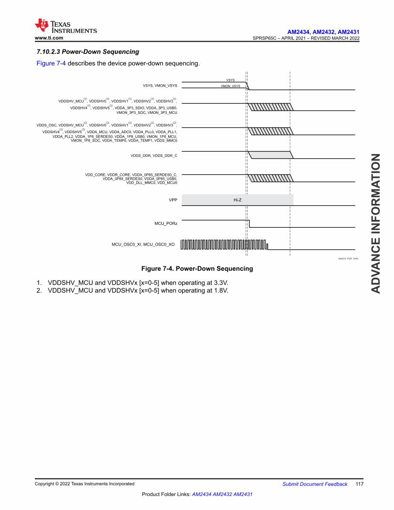
7.10.2.3 Power-Down Sequencing
Figure 7-4 describes the device power-down sequencing.
AM243x_PWR_DWN
MCU_PORz
MCU_OSC0_XI, MCU_OSC0_XO
VSYS
VMON_VSYSVSYS, VMON_VSYS
VPP
VDDSHV_MCU , VDDSHV0 , VDDSHV1 , VDDSHV2 , VDDSHV3 ,(1) (1) (1) (1) (1)
VDDSHV4 , VDDSHV5 , VDDA_3P3_SDIO, VDDA_3P3_USB0,(1) (1)
VMON_3P3_SOC, VMON_3P3_MCU
VDDS_OSC, VDDSHV_MCU , VDDSHV0 , VDDSHV1 , VDDSHV2 , VDDSHV3 ,(2) (2) (2) (2) (2)
VDDSHV4 , VDDSHV5 , VDDA_MCU, VDDA_ADC0, VDDA_PLL0, VDDA_PLL1,(2) (2)
VDDA_PLL2, VDDA_1P8_SERDES0, VDDA_1P8_USB0, VMON_1P8_MCU,VMON_1P8_SOC, VDDA_TEMP0, VDDA_TEMP1, VDDS_MMC0
VDDS_DDR, VDDS_DDR_C
VDD_CORE, VDDR_CORE, VDDA_0P85_SERDES0_C,VDDA_0P85_SERDES0, VDDA_0P85_USB0,
VDD_DLL_MMC0, VDD_MCU0
Hi-Z
Figure 7-4. Power-Down Sequencing
1. VDDSHV_MCU and VDDSHVx [x=0-5] when operating at 3.3V.2. VDDSHV_MCU and VDDSHVx [x=0-5] when operating at 1.8V.
www.ti.comAM2434, AM2432, AM2431
SPRSP65C – APRIL 2021 – REVISED MARCH 2022
AD
VAN
CE
INFO
RM
ATIO
N
Copyright © 2022 Texas Instruments Incorporated Submit Document Feedback 117
Product Folder Links: AM2434 AM2432 AM2431

7.10.3 System Timing
For more details about features and additional description information on the subsystem multiplexing signals, see the corresponding subsections within Signal Descriptions and Detailed Description sections.
Table 7-5. System Timing ConditionsPARAMETER MIN MAX UNIT
INPUT CONDITIONSSRI Input slew rate 0.5 V/ns
OUTPUT CONDITIONSCL Output load capacitance 3 30 pF
AM2434, AM2432, AM2431SPRSP65C – APRIL 2021 – REVISED MARCH 2022 www.ti.com
AD
VAN
CE IN
FOR
MATIO
N
118 Submit Document Feedback Copyright © 2022 Texas Instruments Incorporated
Product Folder Links: AM2434 AM2432 AM2431

7.10.3.1 Reset Timing
Tables and figures provided in this section define timing requirements and switching characteristics for reset related signals.
Table 7-6. MCU_PORz Timing Requirementssee Figure 7-5
NO. PARAMETER MIN MAX UNIT
RST1
th(SUPPLIES_VALID - MCU_PORz)
Hold time, MCU_PORz active (low) at Power-up after supplies valid (using external crystal) 9500000 ns
RST2Hold time, MCU_PORz active (low) at Power-up after supplies valid and external clock stable (using external LVCMOS oscillator)
1200 ns
RST3 tw(MCU_PORzL)
Pulse Width minimum, MCU_PORz low after Power-up (without removal of Power or system reference clock MCU_OSC0_XI/XO)
1200 ns
Figure 7-5. MCU_PORz Timing Requirements
Table 7-7. MCU_RESETSTATz, and RESETSTATz Switching Characteristicssee Figure 7-6
NO. PARAMETER MIN MAX UNIT
RST4 td(MCU_PORzL-MCU_RESETSTATzL)Delay time, MCU_PORz active (low) to MCU_RESETSTATz active (low) 0 ns
RST5 td(MCU_PORzH-MCU_RESETSTATzH)Delay time, MCU_PORz inactive (high) to MCU_RESETSTATz inactive (high) 6120*S(1) ns
RST6 td(MCU_PORzL-RESETSTATzL)Delay time, MCU_PORz active (low) to RESETSTATz active (low) 0 ns
RST7 td(MCU_PORzH-RESETSTATzH)Delay time, MCU_PORz inactive (high) to RESETSTATz inactive (high) 9195*S(1) ns
RST8 tw(MCU_RESETSTATzL)Pulse Width Minimum MCU_RESETSTATz low (SW_MCU_WARMRST) 4040*S(1) ns
RST9 tw(RESETSTATzL)
Pulse Width Minimum RESETSTATz low (SW_MCU_WARMRST, SW_MAIN_PORz, or SW_MAIN_WARMRST)
301200 ns
(1) S = MCU_OSC0_XI/XO clock period
www.ti.comAM2434, AM2432, AM2431
SPRSP65C – APRIL 2021 – REVISED MARCH 2022
AD
VAN
CE
INFO
RM
ATIO
N
Copyright © 2022 Texas Instruments Incorporated Submit Document Feedback 119
Product Folder Links: AM2434 AM2432 AM2431

Figure 7-6. MCU_RESETSTATz, and RESETSTATz Switching Characteristics
Table 7-8. MCU_RESETz Timing Requirementssee Figure 7-7
NO. PARAMETER MIN MAX UNITRST10 tw(MCU_RESETzL) (1) Pulse Width minimum, MCU_RESETz active (low) 1200 ns
(1) This timing parameter is valid only after all supplies are valid and MCU_PORz has been asserted for the specified time.
Table 7-9. MCU_RESETSTATz, and RESETSTATz Switching Characteristicssee Figure 7-7
NO. PARAMETER MIN MAX UNIT
RST11 td(MCU_RESETzL-MCU_RESETSTATzL)Delay time, MCU_RESETz active (low) to MCU_RESETSTATz active (low) 0 ns
RST12 td(MCU_RESETzH-MCU_RESETSTATzH)Delay time, MCU_RESETz inactive (high) to MCU_RESETSTATz inactive (high) 966*S(1) ns
RST13 td(MCU_RESETzL-RESETSTATzL) Delay time, MCU_RESETz active (low) to RESETSTATz active (low) 0 ns
RST14 td(MCU_RESETzH-RESETSTATzH) Delay time, MCU_RESETz inactive (high) to RESETSTATz inactive (high) 4040*S(1) ns
(1) S = MCU_OSC0_XI/XO clock period
Figure 7-7. MCU_RESETz, MCU_RESETSTATz, and RESETSTATz Timing Requirements and Switching Characteristics
AM2434, AM2432, AM2431SPRSP65C – APRIL 2021 – REVISED MARCH 2022 www.ti.com
AD
VAN
CE IN
FOR
MATIO
N
120 Submit Document Feedback Copyright © 2022 Texas Instruments Incorporated
Product Folder Links: AM2434 AM2432 AM2431
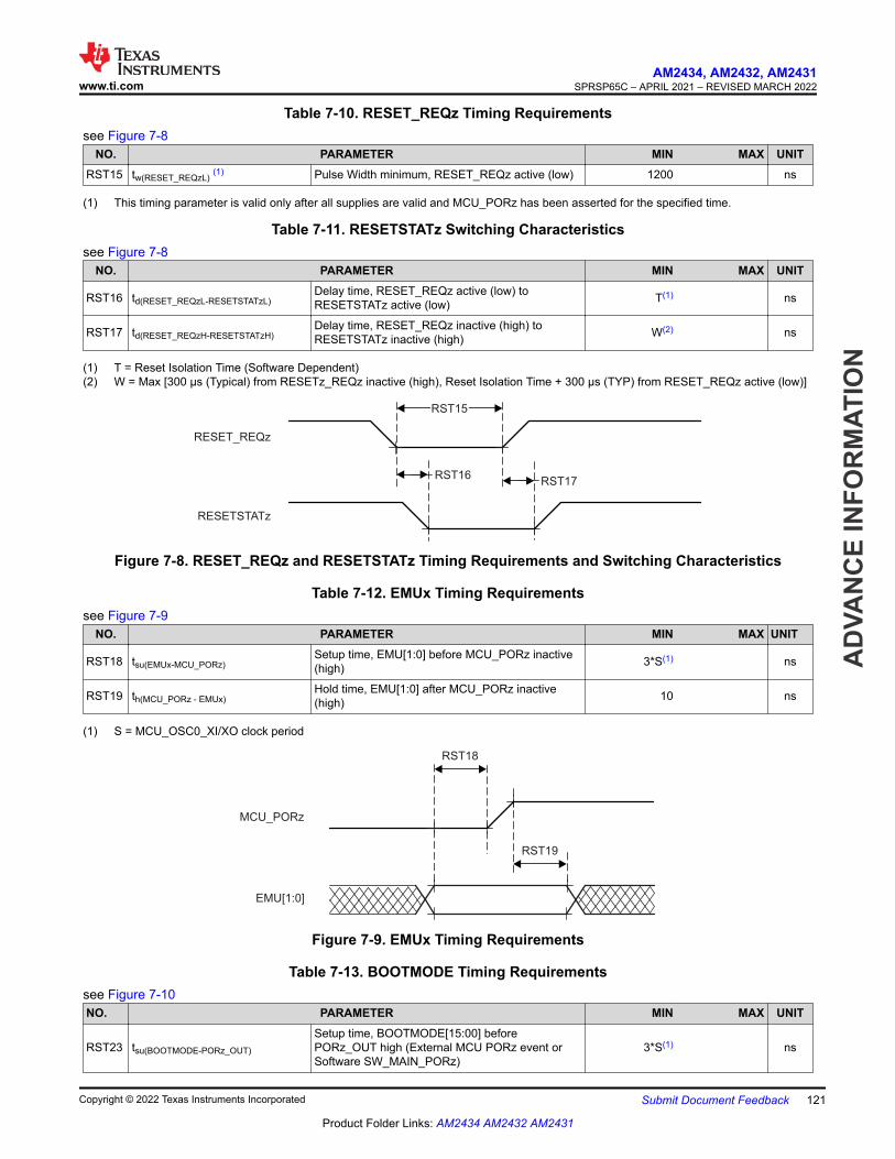
Table 7-10. RESET_REQz Timing Requirementssee Figure 7-8
NO. PARAMETER MIN MAX UNITRST15 tw(RESET_REQzL) (1) Pulse Width minimum, RESET_REQz active (low) 1200 ns
(1) This timing parameter is valid only after all supplies are valid and MCU_PORz has been asserted for the specified time.
Table 7-11. RESETSTATz Switching Characteristicssee Figure 7-8
NO. PARAMETER MIN MAX UNIT
RST16 td(RESET_REQzL-RESETSTATzL)Delay time, RESET_REQz active (low) to RESETSTATz active (low) T(1) ns
RST17 td(RESET_REQzH-RESETSTATzH)Delay time, RESET_REQz inactive (high) to RESETSTATz inactive (high) W(2) ns
(1) T = Reset Isolation Time (Software Dependent)(2) W = Max [300 μs (Typical) from RESETz_REQz inactive (high), Reset Isolation Time + 300 μs (TYP) from RESET_REQz active (low)]
Figure 7-8. RESET_REQz and RESETSTATz Timing Requirements and Switching Characteristics
Table 7-12. EMUx Timing Requirementssee Figure 7-9
NO. PARAMETER MIN MAX UNIT
RST18 tsu(EMUx-MCU_PORz)Setup time, EMU[1:0] before MCU_PORz inactive (high) 3*S(1) ns
RST19 th(MCU_PORz - EMUx)Hold time, EMU[1:0] after MCU_PORz inactive (high) 10 ns
(1) S = MCU_OSC0_XI/XO clock period
Figure 7-9. EMUx Timing Requirements
Table 7-13. BOOTMODE Timing Requirementssee Figure 7-10NO. PARAMETER MIN MAX UNIT
RST23 tsu(BOOTMODE-PORz_OUT)
Setup time, BOOTMODE[15:00] before PORz_OUT high (External MCU PORz event or Software SW_MAIN_PORz)
3*S(1) ns
www.ti.comAM2434, AM2432, AM2431
SPRSP65C – APRIL 2021 – REVISED MARCH 2022
AD
VAN
CE
INFO
RM
ATIO
N
Copyright © 2022 Texas Instruments Incorporated Submit Document Feedback 121
Product Folder Links: AM2434 AM2432 AM2431

Table 7-13. BOOTMODE Timing Requirements (continued)see Figure 7-10NO. PARAMETER MIN MAX UNIT
RST24 th(PORz_OUT - BOOTMODE)
Hold time, BOOTMODE[15:00] after PORz_OUT high (External MCU PORz event, Software SW_MAIN_PORz)
0 ns
(1) S = MCU_OSC0_XI/XO clock period
Table 7-14. PORz_OUT Switching Characteristicssee Figure 7-10NO. PARAMETER MIN MAX UNIT
RST25 td(MCU_PORzL-PORz_OUT)Delay time, MCU_PORz active (low) to PORz_OUT active (low) 0 ns
RST26 td(MCU_PORzH-PORz_OUT)Delay time, MCU_PORz inactive (high) to PORz_OUT inactive (high) 0 ns
RST27 tw(PORz_OUTL)Pulse Width Minimum PORz_OUT low (MCU_PORz, SW_MAIN_PORz) 1200 ns
Figure 7-10. BOOTMODE Timing Requirements and PORz_OUT Switching Characteristics
7.10.3.2 Safety Signal Timing
Tables and figures provided in this section define switching characteristics for MCU_SAFETY_ERRORn.
Table 7-15. MCU_SAFETY_ERRORn Switching Characteristicssee Figure 7-11
NO. PARAMETER MIN MAX UNIT
SFTY1 tc(MCU_SAFETY_ERRORn)Cycle time minimum, MCU_SAFETY_ERRORn (PWM mode enabled) (P*H)+(P*L)(1) (3) (4) ns
SFTY2 tw(MCU_SAFETY_ERRORn)Pulse width minimum, MCU_SAFETY_ERRORn active (PWM mode disabled)(5) P*R(1) (2) ns
SFTY3 td (ERROR_CONDITION-MCU_SAFETY_ERRORnL)
Delay time, ERROR CONDITION to MCU_SAFETY_ERRORn active(5) 50*P(1) ns
(1) P = ESM functional clock(2) R = Error Pin Counter Pre-Load Register count value(3) H = Error Pin PWM High Pre-Load Register count value(4) L = Error Pin PWM Low Pre-Load Register count value(5) When PWM mode is enabled, MCU_SAFETY_ERRORn stops toggling after RST22 and will maintain its value (either high or low) until
the error is cleared. When PWM mode is disabled, MCU_SAFETY_ERRORn is active low.
AM2434, AM2432, AM2431SPRSP65C – APRIL 2021 – REVISED MARCH 2022 www.ti.com
AD
VAN
CE IN
FOR
MATIO
N
122 Submit Document Feedback Copyright © 2022 Texas Instruments Incorporated
Product Folder Links: AM2434 AM2432 AM2431

Figure 7-11. MCU_SAFETY_ERRORn Timing Requirements and Switching Characteristics
7.10.3.3 Clock Timing
Tables and figures provided in this section define timing requirements and switching characteristics for clock signals.
Table 7-16. Clock Timing Requirementssee Figure 7-12
NO. MIN MAX UNITCLK1 tc(EXT_REFCLK1) Cycle time minimum, EXT_REFCLK1 10 ns
CLK2 tw(EXT_REFCLK1H) Pulse Duration minimum, EXT_REFCLK1 high E*0.45(1) E*0.55(1) ns
CLK3 tw(EXT_REFCLK1L) Pulse Duration minimum, EXT_REFCLK1 low E*0.45(1) E*0.55(1) ns
CLK19 tc(MCU_EXT_REFCLK0) Cycle time minimum, MCU_EXT_REFCLK0 10 ns
CLK20 tw(MCU_EXT_REFCLK0H) Pulse Duration minimum, MCU_EXT_REFCLK0 high F*0.45(2) F*0.55(2) ns
CLK21 tw(MCU_EXT_REFCLK0L) Pulse Duration minimum, MCU_EXT_REFCLK0 low F*0.45(2) F*0.55(2) ns
(1) E = EXT_REFCLK1 cycle time(2) F = MCU_EXT_REFCLK0 cycle time
EXT_REFCLK1
CLK1
CLK2 CLK3
CLK19
CLK20 CLK21
MCU_EXT_REFCLK0
Figure 7-12. Clock Timing Requirements
Table 7-17. Clock Switching Characteristicssee Figure 7-13
NO. PARAMETER MIN MAX UNITCLK4 tc(SYSCLKOUT0) Cycle time minimum,SYSCLKOUT0 8 ns
CLK5 tw(SYSCLKOUT0H) Pulse Duration minimum, SYSCLKOUT0 high A*0.4(1) A*0.6(1) ns
CLK6 tw(SYSCLKOUT0L) Pulse Duration minimum, SYSCLKOUT0 low A*0.4(1) A*0.6(1) ns
CLK7 tc(OBSCLK0) Cycle time minimum, OBSCLK0 5 ns
CLK8 tw(OBSCLK0H) Pulse Duration minimum, OBSCLK0 high B*0.45(2) B*0.55(2) ns
CLK9 tw(OBSCLK0L) Pulse Duration minimum,OBSCLK0 low B*0.45(2) B*0.55(2) ns
CLK10 tc(CLKOUT0) Cycle time minimum, CLKOUT0 20 ns
www.ti.comAM2434, AM2432, AM2431
SPRSP65C – APRIL 2021 – REVISED MARCH 2022
AD
VAN
CE
INFO
RM
ATIO
N
Copyright © 2022 Texas Instruments Incorporated Submit Document Feedback 123
Product Folder Links: AM2434 AM2432 AM2431

Table 7-17. Clock Switching Characteristics (continued)see Figure 7-13
NO. PARAMETER MIN MAX UNITCLK11 tw(CLKOUT0H) Pulse Duration minimum, CLKOUT0 high C*0.4(3) C*0.6(3) ns
CLK12 tw(CLKOUT0L) Pulse Duration minimum,CLKOUT0 low C*0.4(3) C*0.6(3) ns
CLK13 tc(MCU_SYSCLKOUT0) Cycle time minimum, MCU_SYSCLKOUT0 10 ns
CLK14 tw(MCU_SYSCLKOUT0H) Pulse Duration minimum, MCU_SYSCLKOUT0 high G*0.4(4) G*0.6(4) ns
CLK15 tw(MCU_SYSCLKOUT0L) Pulse Duration minimum,MCU_SYSCLKOUT0 low G*0.4(4) G*0.6(4) ns
CLK16 tc(MCU_OBSCLK0) Cycle time minimum, MCU_OBSCLK0 5 ns
CLK17 tw(MCU_OBSCLK0H) Pulse Duration minimum, MCU_OBSCLK0 high H*0.45(5) H*0.55(5) ns
CLK18 tw(MCU_OBSCLK0L) Pulse Duration minimum,MCU_OBSCLK0 low H*0.45(5) H*0.55(5) ns
(1) A = SYSCLKOUT0 cycle time(2) B = OBSCLK0 cycle time(3) C = CLKOUT0 cycle time(4) G = MCU_SYSCLKOUT0 cycle time(5) H = MCU_OBSCLK0 cycle time
SYSCLKOUT0
OBSCLK0
CLKOUT0
CLK4
CLK5 CLK6
CLK7
CLK8 CLK9
CLK10
CLK11 CLK12
MCU_SYSCLKOUT0
CLK13
CLK14 CLK15
MCU_OBSCLK0
CLK16
CLK17 CLK18
Figure 7-13. Clock Switching Characteristics
AM2434, AM2432, AM2431SPRSP65C – APRIL 2021 – REVISED MARCH 2022 www.ti.com
AD
VAN
CE IN
FOR
MATIO
N
124 Submit Document Feedback Copyright © 2022 Texas Instruments Incorporated
Product Folder Links: AM2434 AM2432 AM2431

7.10.4 Clock Specifications7.10.4.1 Input Clocks / Oscillators
Various external clock inputs/outputs are needed to drive the device. Summary of these input clock signals is as follows:
• MCU_OSC0_XI/MCU_OSC0_XO — Еxternal main crystal interface pins connected to the internal high-frequency oscillator (MCU_HFOSC0), which is the default clock source for internal reference clock MCU_HFOSC0_CLKOUT.
• General purpose clock inputs– MCU_EXT_REFCLK0 — Optional external system clock input for MCU domain.– EXT_REFCLK1 — Optional external system clock input for MAIN domain.– SERDES0_REFCLK0P/N — Optional SERDES0 reference clock input for PCIe.
• External CPTS reference clock inputs– CP_GEMAC_CPTS0_RFT_CLK — CPTS reference clock input.– CPTS_RFT_CLK — CPTS reference clock input.
Figure 7-14 shows the external input clock sources and the output clocks to peripherals.
DEVICE
MCU_SYSCLKOUT0
Main Domain System Clock (MAIN_SYSCLK0) divided-by-4
External main crystal interface pins connected to internal oscillatorwhich provides reference clock to PLLs within MCU domainand MAIN domain.
MCU Domain System Clock (MCU_SYSCLK0) divided-by-4
MCU_OSC0_XI
MCU_OSC0_XO
SYSCLKOUT0
J7ES_CLOCK_01
TCK
MCU_EXT_REFCLK0 / EXT_REFCLK1 Optional External System Clock Inputs - (MCU Domain) / (MAIN Domain)
JTAG Clock Input
CLKOUT
CPTS Reference Clock InputsCP_GEMAC_CPTS0_RFT_CLK / CPTS0_RFT_CLK
CP_GEMAC_CPTS0_RFT_CLK /CPTS0_RFT_CLK
MCU_PORz
MCU_RESETz MCU Warm Reset Input / Device Warm Reset Input
BOOTMODE[15:00]
MCU Power ON Reset / Device Power ON Reset
Boot Mode Configuration / Devices Select
DDR0_CK0/DDR0_CK0_n DDR Differential Clock Outputs
SERDES0_REFCLK0P/N Optional SERDES0 Reference Clock Input for PCIe
MCU_OBSCLK0 / OBSCLK0 Observation Clock Outputs for MCU Domain Clock / MAIN Domain Clocks
Reference Clock Output
Figure 7-14. Input Clocks Interface
For more information about Input clock interfaces, see Clocking section in Device Configuration chapter in the device TRM.
7.10.4.1.1 MCU_OSC0 Internal Oscillator Clock Source
Figure 7-15 shows the recommended crystal circuit. All discrete components used to implement the oscillator circuit should be placed as close as possible to the MCU_OSC0_XI and MCU_OSC0_XO pins.
www.ti.comAM2434, AM2432, AM2431
SPRSP65C – APRIL 2021 – REVISED MARCH 2022
AD
VAN
CE
INFO
RM
ATIO
N
Copyright © 2022 Texas Instruments Incorporated Submit Document Feedback 125
Product Folder Links: AM2434 AM2432 AM2431

Device
MCU_OSC0_XOMCU_OSC0_XI
CL1
Crystal
CL2
AM65x_MCU_OSC_INT_01
PCB Ground
Figure 7-15. MCU_OSC0 Crystal Implementation
The crystal must be in the fundamental mode of operation and parallel resonant. Table 7-18 summarizes the required electrical constraints.
Table 7-18. MCU_OSC0 Crystal Circuit RequirementsPARAMETER MIN TYP MAX UNIT
Fxtal Crystal Parallel Resonance Frequency 25 MHz
Fxtal Crystal Frequency Stability and Tolerance
Ethernet RGMII and RMII not used ±100
ppmEthernet RGMII and RMII using derived clock ±50
CL1+PCBXI Capacitance of CL1 + CPCBXI 12 24 pF
CL2+PCBXO Capacitance of CL2 + CPCBXO 12 24 pF
CL Crystal Load Capacitance 6 12 pF
Cshunt Crystal Circuit Shunt Capacitance
ESRxtal = 30 Ω 25 MHz 7 pF
ESRxtal = 40 Ω 25 MHz 5 pF
ESRxtal = 50 Ω 25 MHz 5 pF
ESRxtal Crystal Effective Series Resistance (1) Ω
(1) The maximum ESR of the crystal is a function of the crystal frequency and shunt capacitance. See the Cshunt parameter.
When selecting a crystal, the system design must consider temperature and aging characteristics of the crystal based on worst case environment and expected life expectancy of the system.
Table 7-19 details the switching characteristics of the oscillator.
Table 7-19. MCU_OSC0 Switching Characteristics - Crystal ModePARAMETER MIN TYP MAX UNIT
CXI XI Capacitance 1.44 pF
CXO XO Capacitance 1.52 pF
CXIXO XI to XO Mutual Capacitance 0.01 pF
ts Start-up Time 4 ms
AM2434, AM2432, AM2431SPRSP65C – APRIL 2021 – REVISED MARCH 2022 www.ti.com
AD
VAN
CE IN
FOR
MATIO
N
126 Submit Document Feedback Copyright © 2022 Texas Instruments Incorporated
Product Folder Links: AM2434 AM2432 AM2431

VDDS_OSC
MCU_OSC0_XO
tsX
Time
Voltage
VSS
VDDS_OSC (min.)
VDD_CORE (min.)
VSS
VDD_CORE
AM65x_MCU_OSC_STARTUP_02
Figure 7-16. MCU_OSC0 Start-up Time
7.10.4.1.1.1 Load Capacitance
The crystal circuit must be designed such that it applies the appropriate capacitive load to the crystal, as defined by the crystal manufacturer. The capacitive load, CL, of this circuit is a combination of discrete capacitors CL1, CL2, and several parasitic contributions. PCB signal traces which connect crystal circuit components to MCU_OSC0_XI and MCU_OSC0_XO have parasitic capacitance to ground, CPCBXI and CPCBXO, where the PCB designer should be able to extract parasitic capacitance for each signal trace. The MCU_OSC0 circuits and device package have combined parasitic capacitance to ground, CPCBXI and CPCBXO, where these parasitic capacitance values are defined in Table 7-19.
AM65x_MCU_OSC_CC_05
CPCBXI
CPCBXO
CL1
CL2
PCBSignal Traces
Crystal CircuitComponents
MCU_OSC0_XO
MCU_OSC0_XI
CXI
CXO
Device
Figure 7-17. Load Capacitance
Load capacitors, CL1 and CL2 in Figure 7-15, should be chosen such that the below equation is satisfied. CL in the equation is the load specified by the crystal manufacturer.
CL = [(CL1 + CPCBXI + CXI) × (CL2 + CPCBXO + CXO)] / [(CL1 + CPCBXI + CXI) + (CL2 + CPCBXO + CXO)]
To determine the value of CL1 and CL2, multiply the capacitive load value CL by 2. Using this result, subtract the combined values of CPCBXI + CXI to determine the value of CL1 and the combined values of CPCBXO + CXO to determine the value of CL2. For example, if CL = 10 pF, CPCBXI = 2.9 pF, CXI = 0.5 pF, CPCBXO = 3.7 pF, CXO = 0.5 pF, the value of CL1 = [(2CL) - (CPCBXI + CXI)] = [(2 × 10 pF) - 2.9 pF - 0.5 pF)] = 16.6 pF and CL2 = [(2CL) - (CPCBXO + CXO)] = [(2 × 10 pF) - 3.7 pF - 0.5 pF)] = 15.8 pF
www.ti.comAM2434, AM2432, AM2431
SPRSP65C – APRIL 2021 – REVISED MARCH 2022
AD
VAN
CE
INFO
RM
ATIO
N
Copyright © 2022 Texas Instruments Incorporated Submit Document Feedback 127
Product Folder Links: AM2434 AM2432 AM2431

7.10.4.1.1.2 Shunt Capacitance
The crystal circuit must also be designed such that it does not exceed the maximum shunt capacitance for MCU_OSC0 operating conditions defined in Table 7-18. Shunt capacitance, Cshunt, of the crystal circuit is a combination of crystal shunt capacitance and parasitic contributions. PCB signal traces which connect crystal circuit components to MCU_OSC0 have mutual parasitic capacitance to each other, CPCBXIXO, where the PCB designer should be able to extract mutual parasitic capacitance between these signal traces. The device package also has mutual parasitic capacitance, CXIXO, where this mutual parasitic capacitance value is defined in Table 7-19.
PCB routing should be designed to minimize mutual capacitance between XI and XO signal traces. This is typically done by keeping signal traces short and not routing them in close proximity. Mutual capacitance can also be minimized by placing a ground trace between these signals when the layout requires them to be routed in close proximity. It is important to minimize the mutual capacitance on the PCB to provide as much margin as possible when selecting a crystal.
AM65x_MCU_OSC_SC_06
Device
MCU_OSC0_XO
MCU_OSC0_XI
CPCBXIXO
PCBSignal Traces
Crystal CircuitComponents
CXIXOCO
Figure 7-18. Shunt Capacitance
A crystal should be chosen such that the below equation is satisfied. CO in the equation is the maximum shunt capacitance specified by the crystal manufacturer.
Cshunt ≥ CO + CPCBXIXO + CXIXO
For example, the equation would be satisfied when the crystal being used is 25 MHz with an ESR = 30 Ω, CPCBXIXO = 0.04 pF, CXIXO = 0.01 pF, and shunt capacitance of the crystal is less than or equal to 6.95 pF.
7.10.4.1.2 MCU_OSC0 LVCMOS Digital Clock Source
Figure 7-19 shows the recommended oscillator connections when MCU_OSC0_XI is connected to a 1.8-V LVCMOS square-wave digital clock source.
Note
A DC steady-state condition is not allowed on MCU_OSC0_XI when the oscillator is powered up. This is not allowed because MCU_OSC0_XI is internally AC coupled to a comparator that may enter a unknown state when DC is applied to the input. Therefore, application software should power down MCU_OSC0 any time MCU_OSC0_XI is not toggling between logic states.
AM2434, AM2432, AM2431SPRSP65C – APRIL 2021 – REVISED MARCH 2022 www.ti.com
AD
VAN
CE IN
FOR
MATIO
N
128 Submit Document Feedback Copyright © 2022 Texas Instruments Incorporated
Product Folder Links: AM2434 AM2432 AM2431
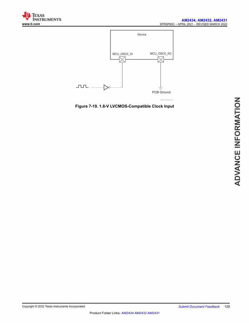
Device
MCU_OSC0_XOMCU_OSC0_XI
AM65x_MCU_OSC_EXT_CLK_03
PCB Ground
Figure 7-19. 1.8-V LVCMOS-Compatible Clock Input
www.ti.comAM2434, AM2432, AM2431
SPRSP65C – APRIL 2021 – REVISED MARCH 2022
AD
VAN
CE
INFO
RM
ATIO
N
Copyright © 2022 Texas Instruments Incorporated Submit Document Feedback 129
Product Folder Links: AM2434 AM2432 AM2431

7.10.4.2 Output Clocks
The device provides several system clock outputs. Summary of these output clocks are as follows:
• MCU_SYSCLKOUT0– MCU_SYSCLKOUT0 is the MCU Domain system clock (MCU_SYSCK0) divided-by-4. This clock output is
provided for test and debug purposes only.• MCU_OBSCLK0
– Observation clock output for test and debug purposes only.• SYSCLKOUT0
– SYSCLKOUT0 is the Main domain system clock (MAIN_SYSCLK0) divided-by-4. This clock output is provided for test and debug purposes only.
• CLKOUT0– CLKOUT0 is the Ethernet Subsytem clock (MAIN_PLL0_HSDIV4_CLKOUT) divided-by-5 or divided-
by-10. This clock output was provided to source to the external PHY. When configured to operate as the RMII Clock source (50 MHz), it must also routed back to the RMII_REF_CLK pin for proper device operation.
• OBSCLK0– Observation clock output for test and debug purposes only.
• GPMC_FCLK_MUX– GPMC_FCLK_MUX is the GPMC0 functional clock (GPMC_FCLK). This clock is provided as an
alternative GPMC interface clock when attached devices require a continuous running clock.
For more information, see Clock Outputs section in Clocking chapter and GPMC Clock Configuration section in Peripherals chapter in the device TRM.
7.10.4.3 PLLs
Power is supplied to the Phase-Locked Loop circuits (PLLs) by internal regulators that derive their power from off-chip power-sources.
There is one PLL in the MCU domain:
• MCU0_PLL
There are six PLLs in the MAIN domain:
• ARM0_PLL• MAIN_PLL• PER0_PLL• PER1_PLL• DDR PLL• R5F PLL
Note
For more information, see:• Device Configuration / Clocking / PLLs section in the device TRM.• Programmable Real-Time Unit Subsystem and Industrial Communication Subsystem - Gigabit
(PRU_ICSSG) section in the device TRM.
Note
The input reference clock (MCU_OSC0_XI / MCU_OSC0_XO) is specified and the lock time is ensured by the PLL controller, as documented in the Device Configuration chapter in the device TRM.
AM2434, AM2432, AM2431SPRSP65C – APRIL 2021 – REVISED MARCH 2022 www.ti.com
AD
VAN
CE IN
FOR
MATIO
N
130 Submit Document Feedback Copyright © 2022 Texas Instruments Incorporated
Product Folder Links: AM2434 AM2432 AM2431

7.10.5 Peripherals7.10.5.1 CPSW3G
For more details about features and additional description information on the device Gigabit Ethernet MAC, see the corresponding subsections within Signal Descriptions and Detailed Description sections.
NoteCPSW3G MDIO0, CPSW3G RMII1, CPSW3G RMII2, and CPSW3G RGMII1 have one or more signals which can be multiplexed to more than one pin. Timing requirements and switching characteristics defined in this section are only valid for specific pin combinations known as IOSETs. Valid pin combinations or IOSETs for these interfaces are shown respectivly in Table 6-7, Table 6-8, and Table 6-9.
7.10.5.1.1 CPSW3G MDIO Timing
Table 7-20, Table 7-21, Table 7-22, and Figure 7-20 present timing conditions, requirements, and switching characteristics for CPSW3G MDIO.
Table 7-20. CPSW3G MDIO Timing ConditionsPARAMETER MIN MAX UNIT
INPUT CONDITIONSSRI Input slew rate 0.9 3.6 V/ns
OUTPUT CONDITIONSCL Output load capacitance 10 470 pF
Table 7-21. CPSW3G MDIO Timing Requirementssee Figure 7-20
NO. PARAMETER MIN MAX UNITMDIO1 tsu(MDIO_MDC) Setup time, MDIO[x]_MDIO valid before MDIO[x]_MDC high 90 ns
MDIO2 th(MDC_MDIO) Hold time, MDIO[x]_MDIO valid after MDIO[x]_MDC high 0 ns
Table 7-22. CPWS3G MDIO Switching Characteristicssee Figure 7-20
NO. PARAMETER MIN MAX UNITMDIO3 tc(MDC) Cycle time, MDIO[x]_MDC 400 ns
MDIO4 tw(MDCH) Pulse Duration, MDIO[x]_MDC high 160 ns
MDIO5 tw(MDCL) Pulse Duration, MDIO[x]_MDC low 160 ns
MDIO7 td(MDC_MDIO) Delay time, MDIO[x]_MDC low to MDIO[x]_MDIO valid -150 150 ns
www.ti.comAM2434, AM2432, AM2431
SPRSP65C – APRIL 2021 – REVISED MARCH 2022
AD
VAN
CE
INFO
RM
ATIO
N
Copyright © 2022 Texas Instruments Incorporated Submit Document Feedback 131
Product Folder Links: AM2434 AM2432 AM2431

MDIO3
MDIO1
MDIO2
MDIO7
MDIO4
MDIO5
MDIO[x]_MDC
MDIO[x]_MDIO(input)
MDIO[x]_MDIO(output)
CPSW2G_MDIO_TIMING_01
Figure 7-20. CPSW3G MDIO Timing Requirements and Switching Characteristics
7.10.5.1.2 CPSW3G RMII Timing
Table 7-23, Table 7-24, Figure 7-21, Table 7-25, Figure 7-22 Table 7-26, and Figure 7-23 present timing conditions, requirements, and switching characteristics for CPSW3G RMII.
Table 7-23. CPSW3G RMII Timing ConditionsPARAMETER MIN MAX UNIT
INPUT CONDITIONS
SRI Input slew rateVDD(1) = 1.8V 0.18 0.54 V/ns
VDD(1) = 3.3V 0.4 1.2 V/ns
OUTPUT CONDITIONSCL Output load capacitance 3 25 pF
(1) VDD stands for corresponding power supply. For more information on the power supply name and the corresponding ball(s), see POWER column of the Pin Attributes table.
Table 7-24. RMII[x]_REF_CLK Timing Requirements – RMII Modesee Figure 7-21
NO. PARAMETER DESCRIPTION MIN MAX UNITRMII1 tc(REF_CLK) Cycle time, RMII[x]_REF_CLK 19.999 20.001 ns
RMII2 tw(REF_CLKH) Pulse Duration, RMII[x]_REF_CLK High 7 13 ns
RMII3 tw(REF_CLKL) Pulse Duration, RMII[x]_REF_CLK Low 7 13 ns
RMII[x]_REF_CLK
RMII2
RMII3
RMII1
Figure 7-21. CPSW3G RMII[x]_REF_CLK Timing Requirements – RMII Mode
AM2434, AM2432, AM2431SPRSP65C – APRIL 2021 – REVISED MARCH 2022 www.ti.com
AD
VAN
CE IN
FOR
MATIO
N
132 Submit Document Feedback Copyright © 2022 Texas Instruments Incorporated
Product Folder Links: AM2434 AM2432 AM2431

Table 7-25. RMII[x]_RXD[1:0], RMII[x]_CRS_DV, and RMII[x]_RX_ER Timing Requirements – RMII Modesee Figure 7-22
NO. PARAMETER DESCRIPTION MIN MAX UNITRMII4 tsu(RXD-REF_CLK) Setup time, RMII[x]_RXD[1:0] valid before RMII[x]_REF_CLK 4 ns
tsu(CRS_DV-REF_CLK) Setup time, RMII[x]_CRS_DV valid before RMII[x]_REF_CLK 4 ns
tsu(RX_ER-REF_CLK) Setup time, RMII[x]_RX_ER valid before RMII[x]_REF_CLK 4 ns
RMII5 th(REF_CLK-RXD) Hold time RMII[x]_RXD[1:0] valid after RMII[x]_REF_CLK 2 ns
th(REF_CLK-CRS_DV) Hold time, RMII[x]_CRS_DV valid after RMII[x]_REF_CLK 2 ns
th(REF_CLK-RX_ER) Hold time, RMII[x]_RX_ER valid after RMII[x]_REF_CLK 2 ns
RMII4
RMII5
RMII[x]_ _REF CLK
RMII[x]_RXD[1:0], RMII[x]_CRS_DV,RMII[x]_RX_ER
Figure 7-22. CPSW3G RMII[x]_RXD[1:0], RMII[x]_CRS_DV, RMII[x]_RX_ER Timing Requirements – RMII Mode
Table 7-26. RMII[x]_TXD[1:0], and RMII[x]_TX_EN Switching Characteristics – RMII Modesee Figure 7-23
NO. PARAMETER DESCRIPTION MIN MAX UNITRMII6 td(REF_CLK-TXD) Delay time, RMII[x]_REF_CLK High to RMII[x]_
TXD[1:0] valid2 10 ns
td(REF_CLK-TX_EN) Delay time, RMII[x]_REF_CLK to RMII[x]_TX_EN valid
2 10 ns
RMII[x]_TXD[1:0], RMII[x]_TX_EN
RMII6
RMII[x]_REF_CLK
Figure 7-23. RMII[x]_TXD[1:0], and RMII[x]_TX_EN Switching Characteristics – RMII Mode
7.10.5.1.3 CPSW3G RGMII Timing
Table 7-27, Table 7-28, Table 7-29, Figure 7-24, Table 7-30, Table 7-31, and Figure 7-25 present timing conditions, requirements, and switching characteristics for CPSW3G RGMII.
Table 7-27. CPSW3G RGMII Timing ConditionsPARAMETER MIN MAX UNIT
INPUT CONDITIONSSRI Input slew rate 2.64 5 V/ns
OUTPUT CONDITIONSCL Output load capacitance 2 20 pF
PCB CONNECTIVITY REQUIREMENTS
www.ti.comAM2434, AM2432, AM2431
SPRSP65C – APRIL 2021 – REVISED MARCH 2022
AD
VAN
CE
INFO
RM
ATIO
N
Copyright © 2022 Texas Instruments Incorporated Submit Document Feedback 133
Product Folder Links: AM2434 AM2432 AM2431

Table 7-27. CPSW3G RGMII Timing Conditions (continued)PARAMETER MIN MAX UNIT
td(Trace Mismatch Delay)
Propagation delay mismatch across all traces
RGMII[x]_RXC, RGMII[x]_RD[3:0], RGMII[x]_RX_CTL
50 ps
RGMII[x]_TXC, RGMII[x]_TD[3:0], RGMII[x]_TX_CTL
50 ps
Table 7-28. RGMII[x]_RXC Timing Requirements – RGMII Modesee Figure 7-24
NO. PARAMETER DESCRIPTION MODE MIN MAX UNITRGMII1 tc(RXC) Cycle time, RGMII[x]_RXC 10Mbps 360 440 ns
100Mbps 36 44 ns
1000Mbps 7.2 8.8 ns
RGMII2 tw(RXCH) Pulse duration, RGMII[x]_RXC high 10Mbps 160 240 ns
100Mbps 16 24 ns
1000Mbps 3.6 4.4 ns
RGMII3 tw(RXCL) Pulse duration, RGMII[x]_RXC low 10Mbps 160 240 ns
100Mbps 16 24 ns
1000Mbps 3.6 4.4 ns
Table 7-29. RGMII[x]_RD[3:0], and RGMII[x]_RX_CTL Timing Requirements – RGMII Modesee Figure 7-24
NO. PARAMETER DESCRIPTION MODE MIN MAX UNITRGMII4 tsu(RD-RXC) Setup time, RGMII[x]_RD[3:0] valid before RGMII[x]_RXC
high/low10Mbps 1 ns
100Mbps 1 ns
1000Mbps 1 ns
tsu(RX_CTL-RXC) Setup time, RGMII[x]_RX_CTL valid before RGMII[x]_RXC high/low
10Mbps 1 ns
100Mbps 1 ns
1000Mbps 1 ns
RGMII5 th(RXC-RD) Hold time, RGMII[x]_RD[3:0] valid after RGMII[x]_RXC high/low
10Mbps 1 ns
100Mbps 1 ns
1000Mbps 1 ns
th(RXC-RX_CTL) Hold time, RGMII[x]_RX_CTL valid after RGMII[x]_RXC high/low
10Mbps 1 ns
100Mbps 1 ns
1000Mbps 1 ns
RGMII[x] RD 3_ [ :0](B)
RGMII[x] RX_CTL_(B)
RGMII[x] RXC_(A)
RGMII4
RXERRRXDV
2nd Half-byte1st Half-byte
RGMII2RGMII3
RGMII1
RGMII5
A. RGMII[x]_RXC must be externally delayed relative to the data and control pins.
AM2434, AM2432, AM2431SPRSP65C – APRIL 2021 – REVISED MARCH 2022 www.ti.com
AD
VAN
CE IN
FOR
MATIO
N
134 Submit Document Feedback Copyright © 2022 Texas Instruments Incorporated
Product Folder Links: AM2434 AM2432 AM2431

B. Data and control information is received using both edges of the clocks. RGMII[x]_RD[3:0] carries data bits 3-0 on the rising edge of RGMII[x]_RXC and data bits 7-4 on the falling edge of RGMII[x]_RXC. Similarly, RGMII[x]_RX_CTL carries RXDV on rising edge of RGMII[x]_RXC and RXERR on falling edge of RGMII[x]_RXC.
Figure 7-24. CPSW3G RGMII[x]_RXC, RGMII[x]_RD[3:0], RGMII[x]_RX_CTL Timing Requirements - RGMII Mode
Table 7-30. RGMII[x]_TXC Switching Characteristics – RGMII Modesee Figure 7-25
NO. PARAMETER DESCRIPTION MODE MIN MAX UNITRGMII6 tc(TXC) Cycle time, RGMII[x]_TXC 10Mbps 360 440 ns
100Mbps 36 44 ns
1000Mbps 7.2 8.8 ns
RGMII7 tw(TXCH) Pulse duration, RGMII[x]_TXC high 10Mbps 160 240 ns
100Mbps 16 24 ns
1000Mbps 3.6 4.4 ns
RGMII8 tw(TXCL) Pulse duration, RGMII[x]_TXC low 10Mbps 160 240 ns
100Mbps 16 24 ns
1000Mbps 3.6 4.4 ns
Table 7-31. RGMII[x]_TD[3:0] and RGMII[x]_TX_CTL Switching Characteristics – RGMII Modesee Figure 7-25
NO. PARAMETER DESCRIPTION MODE MIN MAX UNITRGMII9 tosu(TD-TXC) Output setup time, RGMII[x]_TD[3:0] valid to RGMII[x]_TXC
high/low10Mbps 1.2 ns
100Mbps 1.2 ns
1000Mbps 1.2 ns
tosu(TX_CTL-TXC) Output setup time, RGMII[x]_TX_CTL valid to RGMII[x]_TXC high/low
10Mbps 1.2 ns
100Mbps 1.2 ns
1000Mbps 1.2 ns
RGMII10 toh(TXC-TD) Output hold time, RGMII[x]_TD[3:0] valid after RGMII[x]_TXC high/low
10Mbps 1.2 ns
100Mbps 1.2 ns
1000Mbps 1.2 ns
toh(TXC-TX_CTL) Output hold time, RGMII[x]_TX_CTL valid after RGMII[x]_TXC high/low
10Mbps 1.2 ns
100Mbps 1.2 ns
1000Mbps 1.2 ns
RGMII[x]_TXC(A)
RGMII[x]_TD[3:0](B)
RGMII[x] TX_CTL_(B)
RGMII9
1st Half-byte
TXERRTXEN
2nd Half-byte
RGMII7RGMII8
RGMII6
RGMII10
A. TXC is delayed internally before being driven to the RGMII[x]_TXC pin. This internal delay is always enabled.
www.ti.comAM2434, AM2432, AM2431
SPRSP65C – APRIL 2021 – REVISED MARCH 2022
AD
VAN
CE
INFO
RM
ATIO
N
Copyright © 2022 Texas Instruments Incorporated Submit Document Feedback 135
Product Folder Links: AM2434 AM2432 AM2431

B. Data and control information is received using both edges of the clocks. RGMII[x]_TD[3:0] carries data bits 3-0 on the rising edge of RGMII[x]_TXC and data bits 7-4 on the falling edge of RGMII[x]_TXC. Similarly, RGMII[x]_TX_CTL carries TXEN on rising edge of RGMII[x]_TXC and TXERR on falling edge of RGMII[x]_TXC.
Figure 7-25. CPSW3G RGMII[x]_TXC, RGMII[x]_TD[3:0], and RGMII[x]_TX_CTL Switching Characteristics - RGMII Mode
7.10.5.2 DDRSS
For more details about features and additional description information on the device (LP)DDR4 Memory Interface, see the corresponding subsections within Signal Descriptions and Detailed Description sections.
Table 7-32 and Figure 7-26 present switching characteristics for DDRSS.
Table 7-32. DDRSS Switching Characteristicssee Figure 7-26
NO. PARAMETER DDR TYPE MIN MAX UNIT
1 tc(DDR_CKP/DDR_CKN)
Cycle time, DDR_CKP and DDR_CKNLPDDR4 1.25(1) 20 ns
DDR4 1.25(1) 1.6 ns
(1) Minimum DDR clock Cycle time will be limited based on the specific memory type (vendor) used in a system and by PCB implementation. Refer to AM64x\AM243x DDR Board Design and Layout Guidelines for the proper PCB implementation to achieve maximum DDR frequency.
DDR0_CKP
1
DDR0_CKN
Figure 7-26. DDRSS Switching Characteristics
For more information, see DDR Subsystem (DDRSS) section in Memory Controllers chapter in the device TRM.
7.10.5.3 ECAP
Table 7-33, Table 7-34, Figure 7-27, Table 7-35, and Figure 7-28 present timing conditions, requirements, and switching characteristics for ECAP.
Table 7-33. ECAP Timing ConditionsPARAMETER MIN MAX UNIT
INPUT CONDITIONSSRI Input slew rate 1 4 V/ns
OUTPUT CONDITIONSCL Output load capacitance 2 7 pF
AM2434, AM2432, AM2431SPRSP65C – APRIL 2021 – REVISED MARCH 2022 www.ti.com
AD
VAN
CE IN
FOR
MATIO
N
136 Submit Document Feedback Copyright © 2022 Texas Instruments Incorporated
Product Folder Links: AM2434 AM2432 AM2431

Table 7-34. ECAP Timing Requirementssee Figure 7-27
NO. PARAMETER DESCRIPTION MIN MAX UNITCAP1 tw(CAP) Pulse duration, CAP (asynchronous) 2 + 2P(1) ns
(1) P = sysclk period in ns.
CAP
CAP1
EPERIPHERALS_TIMNG_01
Figure 7-27. ECAP Timings Requirements
Table 7-35. ECAP Switching Characteristicssee Figure 7-28
NO. PARAMETER DESCRIPTION MIN MAX UNITCAP2 tw(APWM) Pulse duration, APWMx high/low -2 + 2P(1) ns
(1) P = sysclk period in ns.
APWM
CAP2
EPERIPHERALS_TIMNG_02
Figure 7-28. ECAP Switching Characteristics
For more information, see Enhanced Capture (ECAP) Module section in Peripherals chapter in the device TRM.
www.ti.comAM2434, AM2432, AM2431
SPRSP65C – APRIL 2021 – REVISED MARCH 2022
AD
VAN
CE
INFO
RM
ATIO
N
Copyright © 2022 Texas Instruments Incorporated Submit Document Feedback 137
Product Folder Links: AM2434 AM2432 AM2431

7.10.5.4 EPWM
Table 7-36, Table 7-37, Figure 7-29, Table 7-38, Figure 7-30, Figure 7-31, and Figure 7-32 present timing conditions, requirements, and switching characteristics for EPWM.
Table 7-36. EPWM Timing ConditionsPARAMETER MIN MAX UNIT
INPUT CONDITIONSSRI Input slew rate 1 4 V/ns
OUTPUT CONDITIONSCL Output load capacitance 2 7 pF
Table 7-37. EPWM Timing Requirementssee Figure 7-29
NO. PARAMETER DESCRIPTION MIN MAX UNITPWM6 tw(SYNCIN) Pulse duration, EHRPWM_SYNCI 2 + 2P(1) ns
PWM7 tw(TZ) Pulse duration, EHRPWM_TZn_IN low 2 + 3P(1) ns
(1) P = sysclk period in ns.
EHRPWM_TZn_IN
PWM7
EPERIPHERALS_TIMNG_07
EHRPWM_SYNCI
PWM6
Figure 7-29. EPWM Timing Requirements
Table 7-38. EPWM Switching Characteristicssee Figure 7-30, Figure 7-31, and Figure 7-32
NO. PARAMETER DESCRIPTION MIN MAX UNITPWM1 tw(PWM) Pulse duration, EHRPWM_A/B high/low P - 3(1) ns
PWM2 tw(SYNCOUT) Pulse duration, EHRPWM_SYNCO P - 3(1) ns
PWM3 td(TZ-PWM) Delay time, EHRPWM_TZn_IN active to EHRPWM_A/B forced high/low
11 ns
PWM4 td(TZ-PWMZ) Delay time, EHRPWM_TZn_IN active to EHRPWM_A/B Hi-Z 11 ns
PWM5 tw(SOC) Pulse duration, EHRPWM_SOCA/B output P - 3(1) ns
(1) P = sysclk period in ns.
AM2434, AM2432, AM2431SPRSP65C – APRIL 2021 – REVISED MARCH 2022 www.ti.com
AD
VAN
CE IN
FOR
MATIO
N
138 Submit Document Feedback Copyright © 2022 Texas Instruments Incorporated
Product Folder Links: AM2434 AM2432 AM2431

EHRPWM_SOCA/B
PWM5
EPERIPHERALS_TIMNG_04
EHRPWM_SYNCO
PWM2
EHRPWM_A/B
PWM1
PWM1
Figure 7-30. EHRPWM Switching Characteristics
EHRPWM_A/B
EHRPWM_TZn_IN
EPERIPHERALS_TIMING_05
PWM3
Figure 7-31. EHRPWM_TZn_IN to EHRPWM_A/B Forced Switching Characteristics
EHRPWM_A/B
EHRPWM_TZn_IN
PWM4
Figure 7-32. EHRPWM_TZn_IN to EHRPWM_A/B Hi-Z Switching Characteristics
For more information, see Enhanced Pulse Width Modulation (EPWM) Module section in Peripherals chapter in the device TRM.
7.10.5.5 EQEP
Table 7-39, Table 7-40, Figure 7-33, and Table 7-41 present timing conditions, requirements, and switching characteristics for EQEP.
Table 7-39. EQEP Timing ConditionsPARAMETER MIN MAX UNIT
INPUT CONDITIONSSRI Input slew rate 1 4 V/ns
OUTPUT CONDITIONSCL Output load capacitance 2 7 pF
Table 7-40. EQEP Timing Requirementssee Figure 7-33
NO. PARAMETER DESCRIPTION MIN MAX UNITQEP1 tw(QEP) Pulse duration, QEP_A/B 2 + 2P(1) ns
QEP2 tw(QEPIH) Pulse duration, QEP_I high 2 + 2P(1) ns
www.ti.comAM2434, AM2432, AM2431
SPRSP65C – APRIL 2021 – REVISED MARCH 2022
AD
VAN
CE
INFO
RM
ATIO
N
Copyright © 2022 Texas Instruments Incorporated Submit Document Feedback 139
Product Folder Links: AM2434 AM2432 AM2431

Table 7-40. EQEP Timing Requirements (continued)see Figure 7-33
NO. PARAMETER DESCRIPTION MIN MAX UNITQEP3 tw(QEPIL) Pulse duration, QEP_I low 2 + 2P(1) ns
QEP4 tw(QEPSH) Pulse duration, QEP_S high 2 + 2P(1) ns
QEP5 tw(QEPSL) Pulse duration, QEP_S low 2 + 2P(1) ns
(1) P = sysclk period in ns
QEP_S
QEP4
EPERIPHERALS_TIMNG_03
QEP_I
QEP2
QEP_A/B
QEP1
QEP3
QEP5
Figure 7-33. EQEP Timing Requirements
Table 7-41. EQEP Switching CharacteristicsNO. PARAMETER DESCRIPTION MIN MAX UNIT
QEP6 td(QEP-CNTR) Delay time, external clock to counter increment 24 ns
For more information, see Enhanced Quadrature Encoder Pulse (EQEP) Module section in Peripherals chapter in the device TRM.
7.10.5.6 FSI
Table 7-42, Table 7-43, Figure 7-34, Table 7-44, Figure 7-35, Table 7-45, and Figure 7-36 present timing conditions, requirements, and switching characteristics for FSI.
Table 7-42. FSI Timing ConditionsPARAMETER MIN MAX UNIT
INPUT CONDITIONSSRI Input slew rate 0.8 4 V/ns
OUTPUT CONDITIONSCL Output load capacitance 1 7 pF
Table 7-43. FSI Timing Requirementssee Figure 7-34
NO. MIN MAX UNITFSIR1 tc(RX_CLK) Cycle time, FSI_RXn_CLK 20 ns
FSIR2 tw(RX_CLK) Pulse width, FSI_RXn_CLK low or FSI_RXn_CLK high 0.5P - 1(1) 0.5P + 1(1) ns
FSIR3 tsu(RX_D-RX_CLK) Setup time, FSI_RXn_D[1:0] valid before FSI_RXn_CLK 3 ns
AM2434, AM2432, AM2431SPRSP65C – APRIL 2021 – REVISED MARCH 2022 www.ti.com
AD
VAN
CE IN
FOR
MATIO
N
140 Submit Document Feedback Copyright © 2022 Texas Instruments Incorporated
Product Folder Links: AM2434 AM2432 AM2431

Table 7-43. FSI Timing Requirements (continued)see Figure 7-34
NO. MIN MAX UNITFSIR4 th(RX_CLK-RX_D) Hold time, FSI_RXn_D[1:0] valid after FSI_RXn_CLK 2.5 ns
(1) P = FSI_RXn_CLK period in ns.
FSI_RXn_CLK
FSIR2
FSIR1
FSIR3
FSI_RXn_D0
FSI_RXn_D1
FSIR4
FSIR2
Figure 7-34. FSI Timing Requirements
Table 7-44. FSI Switching Characteristics - FSI Modesee Figure 7-35
NO. PARAMETER MODE MIN MAX UNITFSIT1 tc(TX_CLK) Cycle time, FSI_TXn_CLK FSI Mode 20 ns
FSIT2 tw(TX_CLK) Pulse width, FSI_TXn_CLK low or FSI_TXn_CLK high FSI Mode 0.5p + 1(1) 0.5P - 1(1) ns
FSIT3 td(TX_CLK-TX_D) Delay time, FSI_TXn_D[1:0] valid after FSI_TXn_CLK high or FSI_TXn_CLK low
FSI Mode 0.25P - 2(1) 0.25P + 2.5(1)
ns
(1) P = FSI_TXn_CLK period in ns.
FSI_TXn_CLK
FSIT2
FSIT1
FSIT3
FSI_TXn_D0
FSI_TXn_D1
FSIT2
FSIT1
Figure 7-35. FSI Switching Characteristics - FSI Mode
Table 7-45. FSI Switching Characteristics - SPI Modesee Figure 7-36
NO. PARAMETER MODE MIN MAX UNITFSIT4 tc(TX_CLK) Cycle time, FSI_TXn_CLK SPI Mode 20 ns
FSIT5 tw(TX_CLK) Pulse width, FSI_TXn_CLK low or FSI_TXn_CLK high SPI Mode 0.5P + 1(1) 0.5P - 1(1) ns
FSIT6 td(TX_CLKH-TX_D0) Delay time, FSI_TXn_CLK high to FSI_TXn_D0 valid SPI Mode 3 ns
FSIT7 td(TX_D1-TX_CLK) Delay time, FSI_TXn_D1 low to FSI_TXn_CLK high SPI Mode P - 3(1) ns
www.ti.comAM2434, AM2432, AM2431
SPRSP65C – APRIL 2021 – REVISED MARCH 2022
AD
VAN
CE
INFO
RM
ATIO
N
Copyright © 2022 Texas Instruments Incorporated Submit Document Feedback 141
Product Folder Links: AM2434 AM2432 AM2431

Table 7-45. FSI Switching Characteristics - SPI Mode (continued)see Figure 7-36
NO. PARAMETER MODE MIN MAX UNITFSIT8 td(TX_CLK-TX_D1) Delay time, FSI_TXn_CLK low to FSI_TXn_D1 high SPI Mode P - 2(1) ns
(1) P = FSI_TXn_CLK period in ns.
FSI_TXn_CLK
FSIT5
FSIT4
FSI_TXn_D0
FSI_TXn_D1
FSIT6
FSIT7FSIT8
FSIT5
Figure 7-36. FSI Switching Characteristics - SPI Mode
For more information, see Fast Serial Interface section in Peripherals chapter in the device TRM.
7.10.5.7 GPIO
Table 7-46, Table 7-47, and Table 7-48 present timing conditions, requirements, and switching characteristics for GPIO.
For more details about features and additional description information on the device GPIO, see the corresponding subsections within Signal Descriptions and Detailed Description sections.
Note
The device has multiple GPIO modules. GPIOn_x is generic name used to describe a GPIO signal, where n represents the specific GPIO module and x represents one of the input/output signals associated with the module.
Table 7-46. GPIO Timing ConditionsPARAMETER BUFFER TYPE MIN MAX UNIT
INPUT CONDITIONS
SRI Input slew rateLVCMOS 0.75 6.6 V/ns
I2C OD FS TBD TBD V/ns
OUTPUT CONDITIONS
CL Output load capacitanceLVCMOS 3 10 pF
I2C OD FS 3 100 pF
Table 7-47. GPIO Timing RequirementsNO. PARAMETER DESCRIPTION BUFFER TYPE MIN MAX UNIT
GPIO1 tw(GPIO_IN) Pulse width, GPIOn_xLVCMOS 2P + 2.6(1) ns
I2C OD FS 2P + 2.6(1) ns
(1) P = functional clock period in ns.
AM2434, AM2432, AM2431SPRSP65C – APRIL 2021 – REVISED MARCH 2022 www.ti.com
AD
VAN
CE IN
FOR
MATIO
N
142 Submit Document Feedback Copyright © 2022 Texas Instruments Incorporated
Product Folder Links: AM2434 AM2432 AM2431

Table 7-48. GPIO Switching CharacteristicsNO. PARAMETER DESCRIPTION BUFFER TYPE MIN MAX UNIT
GPIO2 tw(GPIO_OUT) Pulse width, GPIOn_xLVCMOS -3.6 +
0.975P(1) ns
I2C OD FS 160 ns
(1) P = functional clock period in ns.
For more information, see General-Purpose Interface (GPIO) section in Peripherals chapter in the device TRM.
7.10.5.8 GPMC
For more details about features and additional description information on the device General-Purpose Memory Controller, see the corresponding subsections within Signal Descriptions and Detailed Description sections.
NoteGPMC has one or more signals which can be multiplexed to more than one pin. Timing requirements and switching characteristics defined in this section are only valid for specific pin combinations known as IOSETs. Valid pin combinations or IOSETs for this interface is shown in Table 6-43.
Table 7-49 presents timing conditions for GPMC.
Table 7-49. GPMC Timing ConditionsPARAMETER MIN MAX UNIT
INPUT CONDITIONSSRI Input slew rate 1.65 4 V/ns
OUTPUT CONDITIONSCL Output load capacitance 5 20 pF
PCB CONNECTIVITY REQUIREMENTS
td(Trace Delay) Propagation delay of each trace133 MHz Synchronous Mode 140 360 ps
All other modes 140 720 ps
td(Trace Mismatch Delay)
Propagation delay mismatch across all traces 200 ps
For more information, see General-Purpose Memory Controller (GPMC) section in Peripherals chapter in the device TRM.
7.10.5.8.1 GPMC and NOR Flash — Synchronous Mode
Table 7-50 and Table 7-51 present timing requirements and switching characteristics for GPMC and NOR Flash - Synchronous Mode.
Table 7-50. GPMC and NOR Flash Timing Requirements — Synchronous Modesee Figure 7-37, Figure 7-38, and Figure 7-41
NO. PARAMETER DESCRIPTION MODE(5)MIN MAX MIN MAX
UNITGPMC_FCLK = 100 MHz(2)
GPMC_FCLK = 133 MHz(2)
F12 tsu(dV-clkH) Setup time, input data GPMC_AD[n:0](1) valid before output clock GPMC_CLK high
div_by_1_mode;GPMC_FCLK_MUX;
TIMEPARAGRANULARITY_X1
1.81 1.11 ns
not_div_by_1_mode;GPMC_FCLK_MUX;
TIMEPARAGRANULARITY_X1
1.06 3.50 ns
www.ti.comAM2434, AM2432, AM2431
SPRSP65C – APRIL 2021 – REVISED MARCH 2022
AD
VAN
CE
INFO
RM
ATIO
N
Copyright © 2022 Texas Instruments Incorporated Submit Document Feedback 143
Product Folder Links: AM2434 AM2432 AM2431

Table 7-50. GPMC and NOR Flash Timing Requirements — Synchronous Mode (continued)see Figure 7-37, Figure 7-38, and Figure 7-41
NO. PARAMETER DESCRIPTION MODE(5)MIN MAX MIN MAX
UNITGPMC_FCLK = 100 MHz(2)
GPMC_FCLK = 133 MHz(2)
F13 th(clkH-dV) Hold time, input data GPMC_AD[n:0](1) valid after output clock GPMC_CLK high
div_by_1_mode;GPMC_FCLK_MUX;
TIMEPARAGRANULARITY_X1
2.28 2.28 ns
not_div_by_1_mode;GPMC_FCLK_MUX;
TIMEPARAGRANULARITY_X1
2.28 2.28 ns
F21 tsu(waitV-clkH) Setup time, input wait GPMC_WAIT[j](3) (4) valid before output clock GPMC_CLK high
div_by_1_mode;GPMC_FCLK_MUX;
TIMEPARAGRANULARITY_X1
1.81 1.11 ns
not_div_by_1_mode;GPMC_FCLK_MUX;
TIMEPARAGRANULARITY_X1
1.06 3.50 ns
F22 th(clkH-waitV) Hold time, input wait GPMC_WAIT[j](3) (4) valid after output clock GPMC_CLK high
div_by_1_mode;GPMC_FCLK_MUX;
TIMEPARAGRANULARITY_X1
2.28 2.28 ns
not_div_by_1_mode;GPMC_FCLK_MUX;
TIMEPARAGRANULARITY_X1
2.8 2.28 ns
(1) Synchronous Mode supports 16-bit data bus up to 133 MHz and 32-bit data bus up to 100 MHz(2) GPMC_FCLK select
• gpmc_fclk_sel[1:0] = 2b01 to select the 100MHz GPMC_FCLK• gpmc_fclk_sel[1:0] = 2b00 to select the 133MHz GPMC_FCLK
(3) In GPMC_WAIT[j], j is equal to 0 or 1.(4) Wait monitoring support is limited to a WaitMonitoringTime value > 0. For a full description of wait monitoring feature, see General-
Purpose Memory Controller (GPMC) section in the device TRM.(5) For div_by_1_mode:
• GPMC_CONFIG1_i Register: GPMCFCLKDIVIDER = 0h:– GPMC_CLK frequency = GPMC_FCLK frequency
For not_div_by_1_mode:• GPMC_CONFIG1_i Register: GPMCFCLKDIVIDER = 1h to 3h:
– GPMC_CLK frequency = GPMC_FCLK frequency / (2 to 4)
For GPMC_FCLK_MUX:• CTRLMMR_GPMC_CLKSEL[1-0] CLK_SEL = 01 = PER1_PLL_CLKOUT / 3 = 300 / 3 = 100MHz
For TIMEPARAGRANULARITY_X1:• GPMC_CONFIG1_i Register: TIMEPARAGRANULARITY = 0h = x1 latencies (affecting RD/WRCYCLETIME, RD/
WRACCESSTIME, PAGEBURSTACCESSTIME, CSONTIME, CSRD/WROFFTIME, ADVONTIME, ADVRD/WROFFTIME, OEONTIME, OEOFFTIME, WEONTIME, WEOFFTIME, CYCLE2CYCLEDELAY, BUSTURNAROUND, TIMEOUTSTARTVALUE, WRDATAONADMUXBUS)
Table 7-51. GPMC and NOR Flash Switching Characteristics – Synchronous Modesee Figure 7-37, Figure 7-38, Figure 7-39, Figure 7-40, and Figure 7-41
NO.(3) PARAMETER DESCRIPTION MODE(18) MIN MAX MIN MAX
UNIT100 MHz 133 MHz
F0 1 / tc(clk) Period, output clock GPMC_CLK(16) div_by_1_mode;GPMC_FCLK_MUX;
TIMEPARAGRANULARITY_X1
10.00 7.52 ns
F1 tw(clkH) Typical pulse duration, output clock GPMC_CLK high
div_by_1_mode;GPMC_FCLK_MUX;
TIMEPARAGRANULARITY_X1
0.475P - 0.3(15)
0.475P - 0.3(15)
ns
AM2434, AM2432, AM2431SPRSP65C – APRIL 2021 – REVISED MARCH 2022 www.ti.com
AD
VAN
CE IN
FOR
MATIO
N
144 Submit Document Feedback Copyright © 2022 Texas Instruments Incorporated
Product Folder Links: AM2434 AM2432 AM2431

Table 7-51. GPMC and NOR Flash Switching Characteristics – Synchronous Mode (continued)see Figure 7-37, Figure 7-38, Figure 7-39, Figure 7-40, and Figure 7-41
NO.(3) PARAMETER DESCRIPTION MODE(18) MIN MAX MIN MAX
UNIT100 MHz 133 MHz
F1 tw(clkL) Typical pulse duration, output clock GPMC_CLK low
div_by_1_mode;GPMC_FCLK_MUX;
TIMEPARAGRANULARITY_X1
0.475P - 0.3(15)
0.475P - 0.3(15)
ns
tdc(clk) Duty cycle error, output clock GPMC_CLK
div_by_1_mode;GPMC_FCLK_MUX;
TIMEPARAGRANULARITY_X1
-500.00 500.00 -500.00 500.00 ps
tJ(clk) Jitter standard deviation, output clock GPMC_CLK(17)
div_by_1_mode;GPMC_FCLK_MUX;
TIMEPARAGRANULARITY_X1
33.33 33.33 ps
tR(clk) Rise time, output clock GPMC_CLK div_by_1_mode;GPMC_FCLK_MUX;
TIMEPARAGRANULARITY_X1
2.0 2.0 ns
tF(clk) Fall time, output clock GPMC_CLK div_by_1_mode;GPMC_FCLK_MUX;
TIMEPARAGRANULARITY_X1
2.0 2.0 ns
tR(do) Rise time, output data GPMC_AD[n:0](1)
div_by_1_mode;GPMC_FCLK_MUX;
TIMEPARAGRANULARITY_X1
2.0 2.0 ns
tF(do) Fall time, output data GPMC_AD[n:0](1)
div_by_1_mode;GPMC_FCLK_MUX;
TIMEPARAGRANULARITY_X1
2.0 2.0 ns
F2 td(clkH-csnV) Delay time, output clock GPMC_CLK rising edge to output chip select GPMC_CSn[i] transition(14)
div_by_1_mode;GPMC_FCLK_MUX;
TIMEPARAGRANULARITY_X1;no extra_delay
F - 2.2 (6)
F + 3.75
F - 2.2 (6)
F + 3.75
ns
F3 td(clkH-CSn[i]V) Delay time, output clock GPMC_CLK rising edge to output chip select GPMC_CSn[i] invalid(14)
div_by_1_mode;GPMC_FCLK_MUX;
TIMEPARAGRANULARITY_X1;no extra_delay
E - 2.2 (5)
E + 1.31
E - 2.2 (5)
E + 4.5 ns
F4 td(aV-clk) Delay time, output address GPMC_A[27:1] valid to output clock GPMC_CLK first edge
div_by_1_mode;GPMC_FCLK_MUX;
TIMEPARAGRANULARITY_X1
B - 2.3 (3)
B + 4.5 B - 2.3 (3)
B + 4.5 ns
F5 td(clkH-aIV) Delay time, output clock GPMC_CLK rising edge to output address GPMC_A[27:1] invalid
div_by_1_mode;GPMC_FCLK_MUX;
TIMEPARAGRANULARITY_X1
-2.3 4.5 -2.3 4.5 ns
F6 td(be[x]nV-clk) Delay time, output lower byte enable and command latch enable GPMC_BE0n_CLE, output upper byte enable GPMC_BE1n valid to output clock GPMC_CLK first edge
div_by_1_mode;GPMC_FCLK_MUX;
TIMEPARAGRANULARITY_X1
B - 2.3 (3)
B + 1.9 B - 2.3 (3)
B + 1.9 ns
F7 td(clkH-be[x]nIV) Delay time, output clock GPMC_CLK rising edge to output lower byte enable and command latch enable GPMC_BE0n_CLE, output upper byte enable GPMC_BE1n invalid(11)
div_by_1_mode;GPMC_FCLK_MUX;
TIMEPARAGRANULARITY_X1
D - 2.3(4)
D + 1.9 D - 2.3 (4)
D + 1.9 ns
F7 td(clkL-be[x]nIV) Delay time, GPMC_CLK falling edge to GPMC_BE0n_CLE, GPMC_BE1n invalid(12)
div_by_1_mode;GPMC_FCLK_MUX;
TIMEPARAGRANULARITY_X1
D - 2.3 (4)
D + 1.9 D - 2.3 (4)
D + 1.9 ns
F7 td(clkL-be[x]nIV). Delay time, GPMC_CLK falling edge to GPMC_BE0n_CLE, GPMC_BE1n invalid(13)
div_by_1_mode;GPMC_FCLK_MUX;
TIMEPARAGRANULARITY_X1
D - 2.3 (4)
D + 1.9 D - 2.3 (4)
D + 1.9 ns
F8 td(clkH-advn) Delay time, output clock GPMC_CLK rising edge to output address valid and address latch enable GPMC_ADVn_ALE transition
div_by_1_mode;GPMC_FCLK_MUX;
TIMEPARAGRANULARITY_X1;no extra_delay
G - 2.3(7)
G + 4.5 G - 2.3 (7)
G + 4.5 ns
www.ti.comAM2434, AM2432, AM2431
SPRSP65C – APRIL 2021 – REVISED MARCH 2022
AD
VAN
CE
INFO
RM
ATIO
N
Copyright © 2022 Texas Instruments Incorporated Submit Document Feedback 145
Product Folder Links: AM2434 AM2432 AM2431

Table 7-51. GPMC and NOR Flash Switching Characteristics – Synchronous Mode (continued)see Figure 7-37, Figure 7-38, Figure 7-39, Figure 7-40, and Figure 7-41
NO.(3) PARAMETER DESCRIPTION MODE(18) MIN MAX MIN MAX
UNIT100 MHz 133 MHz
F9 td(clkH-advnIV) Delay time, output clock GPMC_CLK rising edge to output address valid and address latch enable GPMC_ADVn_ALE invalid
div_by_1_mode;GPMC_FCLK_MUX;
TIMEPARAGRANULARITY_X1;no extra_delay
D - 2.3 (4)
D + 4.5 D - 2.3 (4)
D + 4.5 ns
F10 td(clkH-oen) Delay time, output clock GPMC_CLK rising edge to output enable GPMC_OEn_REn transition
div_by_1_mode;GPMC_FCLK_MUX;
TIMEPARAGRANULARITY_X1;no extra_delay
-2.3H (8)
H + 3.5 H - 2.3 (8)
H + 3.5 ns
F11 td(clkH-oenIV) Delay time, output clock GPMC_CLK rising edge to output enable GPMC_OEn_REn invalid
div_by_1_mode;GPMC_FCLK_MUX;
TIMEPARAGRANULARITY_X1;no extra_delay
E - 2.3 (8)
E + 3.5 E - 2.3 (8)
E + 3.5 ns
F14 td(clkH-wen) Delay time, output clock GPMC_CLK rising edge to output write enable GPMC_WEn transition
div_by_1_mode;GPMC_FCLK_MUX;
TIMEPARAGRANULARITY_X1;no extra_delay
I - 2.3 (9)
I + 4.5 I - 2.3 (9)
I + 4.5 ns
F15 td(clkH-do) Delay time, output clock GPMC_CLK rising edge to output data GPMC_AD[n:0](1) transition(11)
div_by_1_mode;GPMC_FCLK_MUX;
TIMEPARAGRANULARITY_X1
J - 2.3 (10)
J + 2.7 J - 2.3 (10)
J + 2.7 ns
F15 td(clkL-do) Delay time, GPMC_CLK falling edge to GPMC_AD[n:0](1) data bus transition(12)
div_by_1_mode;GPMC_FCLK_MUX;
TIMEPARAGRANULARITY_X1
J - 2.3 (10)
J + 2.7 J - 2.3 (10)
J + 2.7 ns
F15 td(clkL-do). Delay time, GPMC_CLK falling edge to GPMC_AD[n:0](1) data bus transition(13)
div_by_1_mode;GPMC_FCLK_MUX;
TIMEPARAGRANULARITY_X1
J - 2.3 (10)
J + 2.7 J - 2.3 (10)
J + 2.7 ns
F17 td(clkH-be[x]n) Delay time, output clock GPMC_CLK rising edge to output lower byte enable and command latch enable GPMC_BE0n_CLE transition(11)
div_by_1_mode;GPMC_FCLK_MUX;
TIMEPARAGRANULARITY_X1
J - 2.3 (10)
J + 1.9 J - 2.3 (10)
J + 1.9 ns
F17 td(clkL-be[x]n) Delay time, GPMC_CLK falling edge to GPMC_BE0n_CLE, GPMC_BE1n transition(12)
div_by_1_mode;GPMC_FCLK_MUX;
TIMEPARAGRANULARITY_X1
J - 2.3 (10)
J + 1.9 J - 2.3 (10)
J + 1.9 ns
F17 td(clkL-be[x]n). Delay time, GPMC_CLK falling edge to GPMC_BE0n_CLE, GPMC_BE1n transition(13)
div_by_1_mode;GPMC_FCLK_MUX;
TIMEPARAGRANULARITY_X1
J - 2.3 (10)
J + 1.9 J - 2.3 (10)
J + 1.9 ns
F18 tw(csnV) Pulse duration, output chip select GPMC_CSn[i](14) low
Read A A ns
Write A A ns
F19 tw(be[x]nV) Pulse duration, output lower byte enable and command latch enable GPMC_BE0n_CLE, output upper byte enable GPMC_BE1n low
Read C C ns
Write C C ns
F20 tw(advnV) Pulse duration, output address valid and address latch enable GPMC_ADVn_ALE low
Read K K ns
Write K K ns
(1) Synchronous Mode supports 16-bit data bus up to 133 MHz and 32-bit data bus up to 100 MHz(2) For single read: A = (CSRdOffTime - CSOnTime) × (TimeParaGranularity + 1) × GPMC_FCLK(15)
For burst read: A = (CSRdOffTime - CSOnTime + (n - 1) × PageBurstAccessTime) × (TimeParaGranularity + 1) × GPMC_FCLK(15)
For burst write: A = (CSWrOffTime - CSOnTime + (n - 1) × PageBurstAccessTime) × (TimeParaGranularity + 1) × GPMC_FCLK(15)
With n being the page burst access number.(3) B = ClkActivationTime × GPMC_FCLK(15)
(4) For single read: D = (RdCycleTime - AccessTime) × (TimeParaGranularity + 1) × GPMC_FCLK(15)
For burst read: D = (RdCycleTime - AccessTime) × (TimeParaGranularity + 1) × GPMC_FCLK(15)
For burst write: D = (WrCycleTime - AccessTime) × (TimeParaGranularity + 1) × GPMC_FCLK(15)
(5) For single read: E = (CSRdOffTime - AccessTime) × (TimeParaGranularity + 1) × GPMC_FCLK(15)
For burst read: E = (CSRdOffTime - AccessTime) × (TimeParaGranularity + 1) × GPMC_FCLK(15)
For burst write: E = (CSWrOffTime - AccessTime) × (TimeParaGranularity + 1) × GPMC_FCLK(15)
AM2434, AM2432, AM2431SPRSP65C – APRIL 2021 – REVISED MARCH 2022 www.ti.com
AD
VAN
CE IN
FOR
MATIO
N
146 Submit Document Feedback Copyright © 2022 Texas Instruments Incorporated
Product Folder Links: AM2434 AM2432 AM2431

(6) For csn falling edge (CS activated):• Case GPMCFCLKDIVIDER = 0:
– F = 0.5 × CSExtraDelay × GPMC_FCLK(15)
• Case GPMCFCLKDIVIDER = 1:– F = 0.5 × CSExtraDelay × GPMC_FCLK(15) if (ClkActivationTime and CSOnTime are odd) or (ClkActivationTime and
CSOnTime are even)– F = (1 + 0.5 × CSExtraDelay) × GPMC_FCLK(15) otherwise
• Case GPMCFCLKDIVIDER = 2:– F = 0.5 × CSExtraDelay × GPMC_FCLK(15) if ((CSOnTime - ClkActivationTime) is a multiple of 3)– F = (1 + 0.5 × CSExtraDelay) × GPMC_FCLK(15) if ((CSOnTime - ClkActivationTime - 1) is a multiple of 3)– F = (2 + 0.5 × CSExtraDelay) × GPMC_FCLK(15) if ((CSOnTime - ClkActivationTime - 2) is a multiple of 3)
(7) For ADV falling edge (ADV activated):• Case GPMCFCLKDIVIDER = 0:
– G = 0.5 × ADVExtraDelay × GPMC_FCLK(15)
• Case GPMCFCLKDIVIDER = 1:– G = 0.5 × ADVExtraDelay × GPMC_FCLK(15) if (ClkActivationTime and ADVOnTime are odd) or (ClkActivationTime and
ADVOnTime are even)– G = (1 + 0.5 × ADVExtraDelay) × GPMC_FCLK(15) otherwise
• Case GPMCFCLKDIVIDER = 2:– G = 0.5 × ADVExtraDelay × GPMC_FCLK(15) if ((ADVOnTime - ClkActivationTime) is a multiple of 3)– G = (1 + 0.5 × ADVExtraDelay) × GPMC_FCLK(15) if ((ADVOnTime - ClkActivationTime - 1) is a multiple of 3)– G = (2 + 0.5 × ADVExtraDelay) × GPMC_FCLK(15) if ((ADVOnTime - ClkActivationTime - 2) is a multiple of 3)
For ADV rising edge (ADV deactivated) in Reading mode:• Case GPMCFCLKDIVIDER = 0:
– G = 0.5 × ADVExtraDelay × GPMC_FCLK(15)
• Case GPMCFCLKDIVIDER = 1:– G = 0.5 × ADVExtraDelay × GPMC_FCLK(15) if (ClkActivationTime and ADVRdOffTime are odd) or (ClkActivationTime and
ADVRdOffTime are even)– G = (1 + 0.5 × ADVExtraDelay) × GPMC_FCLK(15) otherwise
• Case GPMCFCLKDIVIDER = 2:– G = 0.5 × ADVExtraDelay × GPMC_FCLK(15) if ((ADVRdOffTime - ClkActivationTime) is a multiple of 3)– G = (1 + 0.5 × ADVExtraDelay) × GPMC_FCLK(15) if ((ADVRdOffTime - ClkActivationTime - 1) is a multiple of 3)– G = (2 + 0.5 × ADVExtraDelay) × GPMC_FCLK(15) if ((ADVRdOffTime - ClkActivationTime - 2) is a multiple of 3)
For ADV rising edge (ADV deactivated) in Writing mode:• Case GPMCFCLKDIVIDER = 0:
– G = 0.5 × ADVExtraDelay × GPMC_FCLK(15)
• Case GPMCFCLKDIVIDER = 1:– G = 0.5 × ADVExtraDelay × GPMC_FCLK(15) if (ClkActivationTime and ADVWrOffTime are odd) or (ClkActivationTime and
ADVWrOffTime are even)– G = (1 + 0.5 × ADVExtraDelay) × GPMC_FCLK(15) otherwise
• Case GPMCFCLKDIVIDER = 2:– G = 0.5 × ADVExtraDelay × GPMC_FCLK(15) if ((ADVWrOffTime - ClkActivationTime) is a multiple of 3)– G = (1 + 0.5 × ADVExtraDelay) × GPMC_FCLK(15) if ((ADVWrOffTime - ClkActivationTime - 1) is a multiple of 3)– G = (2 + 0.5 × ADVExtraDelay) × GPMC_FCLK(15) if ((ADVWrOffTime - ClkActivationTime - 2) is a multiple of 3)
(8) For OE falling edge (OE activated) and IO DIR rising edge (Data Bus input direction):• Case GPMCFCLKDIVIDER = 0:
– H = 0.5 × OEExtraDelay × GPMC_FCLK(15)
• Case GPMCFCLKDIVIDER = 1:– H = 0.5 × OEExtraDelay × GPMC_FCLK(15) if (ClkActivationTime and OEOnTime are odd) or (ClkActivationTime and
OEOnTime are even)– H = (1 + 0.5 × OEExtraDelay) × GPMC_FCLK(15) otherwise
• Case GPMCFCLKDIVIDER = 2:– H = 0.5 × OEExtraDelay × GPMC_FCLK(15) if ((OEOnTime - ClkActivationTime) is a multiple of 3)
www.ti.comAM2434, AM2432, AM2431
SPRSP65C – APRIL 2021 – REVISED MARCH 2022
AD
VAN
CE
INFO
RM
ATIO
N
Copyright © 2022 Texas Instruments Incorporated Submit Document Feedback 147
Product Folder Links: AM2434 AM2432 AM2431

– H = (1 + 0.5 × OEExtraDelay) × GPMC_FCLK(15) if ((OEOnTime - ClkActivationTime - 1) is a multiple of 3)– H = (2 + 0.5 × OEExtraDelay) × GPMC_FCLK(15) if ((OEOnTime - ClkActivationTime - 2) is a multiple of 3)
For OE rising edge (OE deactivated):• Case GPMCFCLKDIVIDER = 0:
– H = 0.5 × OEExtraDelay × GPMC_FCLK(15)
• Case GPMCFCLKDIVIDER = 1:– H = 0.5 × OEExtraDelay × GPMC_FCLK(15) if (ClkActivationTime and OEOffTime are odd) or (ClkActivationTime and
OEOffTime are even)– H = (1 + 0.5 × OEExtraDelay) × GPMC_FCLK(15) otherwise
• Case GPMCFCLKDIVIDER = 2:– H = 0.5 × OEExtraDelay × GPMC_FCLK(15) if ((OEOffTime - ClkActivationTime) is a multiple of 3)– H = (1 + 0.5 × OEExtraDelay) × GPMC_FCLK(15) if ((OEOffTime - ClkActivationTime - 1) is a multiple of 3)– H = (2 + 0.5 × OEExtraDelay) × GPMC_FCLK(15) if ((OEOffTime - ClkActivationTime - 2) is a multiple of 3)
(9) For WE falling edge (WE activated):• Case GPMCFCLKDIVIDER = 0:
– I = 0.5 × WEExtraDelay × GPMC_FCLK(15)
• Case GPMCFCLKDIVIDER = 1:– I = 0.5 × WEExtraDelay × GPMC_FCLK(15) if (ClkActivationTime and WEOnTime are odd) or (ClkActivationTime and
WEOnTime are even)– I = (1 + 0.5 × WEExtraDelay) × GPMC_FCLK(15) otherwise
• Case GPMCFCLKDIVIDER = 2:– I = 0.5 × WEExtraDelay × GPMC_FCLK(15) if ((WEOnTime - ClkActivationTime) is a multiple of 3)– I = (1 + 0.5 × WEExtraDelay) × GPMC_FCLK(15) if ((WEOnTime - ClkActivationTime - 1) is a multiple of 3)– I = (2 + 0.5 × WEExtraDelay) × GPMC_FCLK(15) if ((WEOnTime - ClkActivationTime - 2) is a multiple of 3)
For WE rising edge (WE deactivated):• Case GPMCFCLKDIVIDER = 0:
– I = 0.5 × WEExtraDelay × GPMC_FCLK (15)
• Case GPMCFCLKDIVIDER = 1:– I = 0.5 × WEExtraDelay × GPMC_FCLK(15) if (ClkActivationTime and WEOffTime are odd) or (ClkActivationTime and
WEOffTime are even)– I = (1 + 0.5 × WEExtraDelay) × GPMC_FCLK(15) otherwise
• Case GPMCFCLKDIVIDER = 2:– I = 0.5 × WEExtraDelay × GPMC_FCLK(15) if ((WEOffTime - ClkActivationTime) is a multiple of 3)– I = (1 + 0.5 × WEExtraDelay) × GPMC_FCLK(15) if ((WEOffTime - ClkActivationTime - 1) is a multiple of 3)– I = (2 + 0.5 × WEExtraDelay) × GPMC_FCLK(15) if ((WEOffTime - ClkActivationTime - 2) is a multiple of 3)
(10) J = GPMC_FCLK(15)
(11) First transfer only for CLK DIV 1 mode.(12) Half cycle; for all data after initial transfer for CLK DIV 1 mode.(13) Half cycle of GPMC_CLKOUT; for all data for modes other than CLK DIV 1 mode. GPMC_CLKOUT divide down from GPMC_FCLK.(14) In GPMC_CSn[i], i is equal to 0, 1, 2 or 3. In GPMC_WAIT[j], j is equal to 0 or 1.(15) P = GPMC_CLK period in ns(16) Related to the GPMC_CLK output clock maximum and minimum frequencies programmable in the GPMC module by setting the
GPMC_CONFIG1_i configuration register bit field GPMCFCLKDIVIDER.(17) The jitter probability density can be approximated by a Gaussian function.(18) For div_by_1_mode:
• GPMC_CONFIG1_i register: GPMCFCLKDIVIDER = 0h:– GPMC_CLK frequency = GPMC_FCLK frequency
For GPMC_FCLK_MUX:• CTRLMMR_GPMC_CLKSEL[1-0] CLK_SEL = 01 = PER1_PLL_CLKOUT / 3 = 300 / 3 = 100MHz
For TIMEPARAGRANULARITY_X1:• GPMC_CONFIG1_i Register: TIMEPARAGRANULARITY = 0h = x1 latencies (affecting RD/WRCYCLETIME, RD/
WRACCESSTIME, PAGEBURSTACCESSTIME, CSONTIME, CSRD/WROFFTIME, ADVONTIME, ADVRD/WROFFTIME, OEONTIME, OEOFFTIME, WEONTIME, WEOFFTIME, CYCLE2CYCLEDELAY, BUSTURNAROUND, TIMEOUTSTARTVALUE, WRDATAONADMUXBUS)
AM2434, AM2432, AM2431SPRSP65C – APRIL 2021 – REVISED MARCH 2022 www.ti.com
AD
VAN
CE IN
FOR
MATIO
N
148 Submit Document Feedback Copyright © 2022 Texas Instruments Incorporated
Product Folder Links: AM2434 AM2432 AM2431

For no extra_delay:• GPMC_CONFIG2_i Register: CSEXTRADELAY = 0h = CSn Timing control signal is not delayed• GPMC_CONFIG4_i Register: WEEXTRADELAY = 0h = nWE timing control signal is not delayed• GPMC_CONFIG4_i Register: OEEXTRADELAY = 0h = nOE timing control signal is not delayed• GPMC_CONFIG3_i Register: ADVEXTRADELAY = 0h = nADV timing control signal is not delayed
GPMC_CLK
GPMC_CSn[i]
GPMC_A[MSB:1]
GPMC_BE0n_CLE
GPMC_BE1n
GPMC_ADVn_ALE
GPMC_OEn_REn
GPMC_AD[15:0]
GPMC_WAIT[j]
Valid Address
D 0
F0
F12
F13
F4
F6
F2
F8
F3
F7
F9
F11
F1
F1
F8
F19
F18
F20
F10
F6
F19
F12F12
GPMC_01
A. In GPMC_CSn[i], i is equal to 0, 1, 2 or 3.B. In GPMC_WAIT[j], j is equal to 0 or 1.
Figure 7-37. GPMC and NOR Flash — Synchronous Single Read (GPMCFCLKDIVIDER = 0)
www.ti.comAM2434, AM2432, AM2431
SPRSP65C – APRIL 2021 – REVISED MARCH 2022
AD
VAN
CE
INFO
RM
ATIO
N
Copyright © 2022 Texas Instruments Incorporated Submit Document Feedback 149
Product Folder Links: AM2434 AM2432 AM2431

GPMC_CLK
GPMC_CSn[i]
GPMCA[MSB:1]
GPMC_BE0n_CLE
GPMC_BE1n
GPMC_ADVn_ALE
GPMC_OEn_REn
GPMC_AD[15:0]
GPMC_WAIT[j]
Valid Address
D 0 D 1 D 2
F0
F12
F13 F13
F12
F4
F1
F1
F2
F6
F3
F7
F8 F8 F9
F10 F11
F21 F22
F6
F7
D 3
GPMC_02
A. In GPMC_CSn[i], i is equal to 0, 1, 2 or 3.B. In GPMC_WAIT[j], j is equal to 0 or 1.
Figure 7-38. GPMC and NOR Flash — Synchronous Burst Read — 4x16–bit (GPMCFCLKDIVIDER = 0)
GPMC_CLK
GPMC_CSn[i]
GPMC_A[MSB:1]
GPMC_BE0n_CLE
GPMC_BE1n
GPMC_ADVn_ALE
GPMC_WEn
GPMC_AD[15:0]
GPMC_WAIT[j]
D 0 D 1 D 2 D 3
F4
F15 F15 F15
F1
F1
F2
F6
F8F8
F0
F14F14
F3
F17
F17
F17
F9F6
F17
F17
F17
Valid Address
GPMC_03
A. In GPMC_CSn[i], i is equal to 0, 1, 2 or 3.
AM2434, AM2432, AM2431SPRSP65C – APRIL 2021 – REVISED MARCH 2022 www.ti.com
AD
VAN
CE IN
FOR
MATIO
N
150 Submit Document Feedback Copyright © 2022 Texas Instruments Incorporated
Product Folder Links: AM2434 AM2432 AM2431

B. In GPMC_WAIT[j], j is equal to 0 or 1.
Figure 7-39. GPMC and NOR Flash—Synchronous Burst Write (GPMCFCLKDIVIDER = 0)
GPMC_CLK
GPMC_CSn[i]
GMPC_BE0n_CLE
GPMC_BE1n
GPMC_A[27:17]
GPMC_AD[15:0]
GPMC_ADVn_ALE
GPMC_OEn_REn
GPMC_WAIT[j]
Valid
Valid
Address (MSB)
Address (LSB) D0 D1 D2 D3
F4
F6
F4
F2
F8 F8
F10
F13
F12
F12
F11
F9
F7
F3
F0 F1
F1
F5
F6 F7
GPMC_04
A. In GPMC_CSn[i], i is equal to 0, 1, 2 or 3.B. In GPMC_WAIT[j], j is equal to 0 or 1.
Figure 7-40. GPMC and Multiplexed NOR Flash — Synchronous Burst Read
www.ti.comAM2434, AM2432, AM2431
SPRSP65C – APRIL 2021 – REVISED MARCH 2022
AD
VAN
CE
INFO
RM
ATIO
N
Copyright © 2022 Texas Instruments Incorporated Submit Document Feedback 151
Product Folder Links: AM2434 AM2432 AM2431
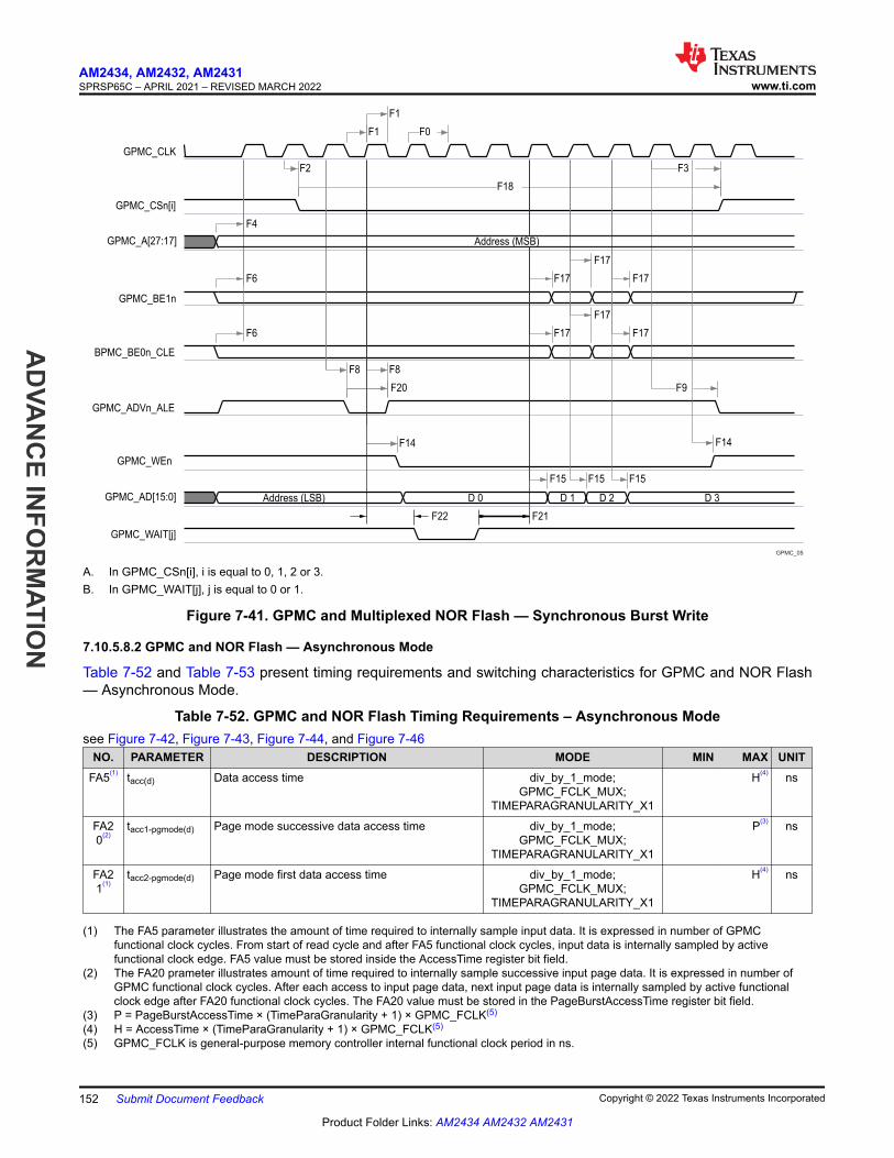
GPMC_CLK
GPMC_CSn[i]
GPMC_A[27:17]
GPMC_BE1n
BPMC_BE0n_CLE
GPMC_ADVn_ALE
GPMC_WEn
GPMC_WAIT[j]
Address (LSB) D 0 D 1 D 2 D 3
F4
F15 F15 F15
F1
F1
F2
F6
F8F8
F0
F3
F17
F17
F17
F9
F6 F17
F17
F17
F18
F20
F14
F22 F21
Address (MSB)
GPMC_AD[15:0]
F14
GPMC_05
A. In GPMC_CSn[i], i is equal to 0, 1, 2 or 3.B. In GPMC_WAIT[j], j is equal to 0 or 1.
Figure 7-41. GPMC and Multiplexed NOR Flash — Synchronous Burst Write
7.10.5.8.2 GPMC and NOR Flash — Asynchronous Mode
Table 7-52 and Table 7-53 present timing requirements and switching characteristics for GPMC and NOR Flash — Asynchronous Mode.
Table 7-52. GPMC and NOR Flash Timing Requirements – Asynchronous Modesee Figure 7-42, Figure 7-43, Figure 7-44, and Figure 7-46
NO. PARAMETER DESCRIPTION MODE MIN MAX UNITFA5(1) tacc(d) Data access time div_by_1_mode;
GPMC_FCLK_MUX;TIMEPARAGRANULARITY_X1
H(4) ns
FA20(2)
tacc1-pgmode(d) Page mode successive data access time div_by_1_mode;GPMC_FCLK_MUX;
TIMEPARAGRANULARITY_X1
P(3) ns
FA21(1)
tacc2-pgmode(d) Page mode first data access time div_by_1_mode;GPMC_FCLK_MUX;
TIMEPARAGRANULARITY_X1
H(4) ns
(1) The FA5 parameter illustrates the amount of time required to internally sample input data. It is expressed in number of GPMC functional clock cycles. From start of read cycle and after FA5 functional clock cycles, input data is internally sampled by active functional clock edge. FA5 value must be stored inside the AccessTime register bit field.
(2) The FA20 prameter illustrates amount of time required to internally sample successive input page data. It is expressed in number of GPMC functional clock cycles. After each access to input page data, next input page data is internally sampled by active functional clock edge after FA20 functional clock cycles. The FA20 value must be stored in the PageBurstAccessTime register bit field.
(3) P = PageBurstAccessTime × (TimeParaGranularity + 1) × GPMC_FCLK(5)
(4) H = AccessTime × (TimeParaGranularity + 1) × GPMC_FCLK(5)
(5) GPMC_FCLK is general-purpose memory controller internal functional clock period in ns.
AM2434, AM2432, AM2431SPRSP65C – APRIL 2021 – REVISED MARCH 2022 www.ti.com
AD
VAN
CE IN
FOR
MATIO
N
152 Submit Document Feedback Copyright © 2022 Texas Instruments Incorporated
Product Folder Links: AM2434 AM2432 AM2431

Table 7-53. GPMC and NOR Flash Switching Characteristics – Asynchronous Modesee Figure 7-42, Figure 7-43, Figure 7-44, Figure 7-45, Figure 7-46, and Figure 7-47
NO. PARAMETER DESCRIPTION MODE(15) MIN MAXUNIT
133 MHztR(d) Rise time, output data GPMC_AD[15:0] div_by_1_mode;
GPMC_FCLK_MUX;TIMEPARAGRANULARITY_X1
2.0 ns
tF(d) Fall time, output data GPMC_AD[15:0] div_by_1_mode;GPMC_FCLK_MUX;
TIMEPARAGRANULARITY_X1
2.0 ns
FA0 tw(be[x]nV) Pulse duration, output lower-byte enable and command latch enable GPMC_BE0n_CLE, output upper-byte enable GPMC_BE1n valid time
Read N (12) ns
Write N (12)
FA1 tw(csnV) Pulse duration, output chip select GPMC_CSn[i](13)
lowRead A (1) ns
Write A (1)
FA3 td(csnV-advnIV) Delay time, output chip select GPMC_CSn[i](13)
valid to output address valid and address latch enable GPMC_ADVn_ALE invalid
Read B - 2.1 (2)
B + 2.1 (2)
ns
Write B - 2.1 (2)
B + 2.1 (2)
FA4 td(csnV-oenIV) Delay time, output chip select GPMC_CSn[i](13)
valid to output enable GPMC_OEn_REn invalid (Single read)
div_by_1_mode;GPMC_FCLK_MUX;
TIMEPARAGRANULARITY_X1
C - 2.1 (3)
C + 2.1 (3)
ns
FA9 td(aV-csnV) Delay time, output address GPMC_A[27:1] valid to output chip select GPMC_CSn[i](13) valid
div_by_1_mode;GPMC_FCLK_MUX;
TIMEPARAGRANULARITY_X1
J - 2.1 (9) J + 2.1 (9)
ns
FA10 td(be[x]nV-csnV) Delay time, output lower-byte enable and command latch enable GPMC_BE0n_CLE, output upper-byte enable GPMC_BE1n valid to output chip select GPMC_CSn[i](13) valid
div_by_1_mode;GPMC_FCLK_MUX;
TIMEPARAGRANULARITY_X1
J - 2.1 (9) J + 2.1 (9)
ns
FA12 td(csnV-advnV) Delay time, output chip select GPMC_CSn[i](13)
valid to output address valid and address latch enable GPMC_ADVn_ALE valid
div_by_1_mode;GPMC_FCLK_MUX;
TIMEPARAGRANULARITY_X1
K - 2.1 (10)
K + 2.1 (10)
ns
FA13 td(csnV-oenV) Delay time, output chip select GPMC_CSn[i](13)
valid to output enable GPMC_OEn_REn validdiv_by_1_mode;
GPMC_FCLK_MUX;TIMEPARAGRANULARITY_X1
L - 2.1 (11)
L + 2.1 (11)
ns
FA16 tw(aIV) Pulse duration output address GPMC_A[26:1] invalid between 2 successive read and write accesses
div_by_1_mode;GPMC_FCLK_MUX;
TIMEPARAGRANULARITY_X1
G (7) ns
FA18 td(csnV-oenIV) Delay time, output chip select GPMC_CSn[i](13)
valid to output enable GPMC_OEn_REn invalid (Burst read)
div_by_1_mode;GPMC_FCLK_MUX;
TIMEPARAGRANULARITY_X1
I - 2.1 (8) I + 2.1 (8) ns
FA20 tw(aV) Pulse duration, output address GPMC_A[27:1] valid - 2nd, 3rd, and 4th accesses
div_by_1_mode;GPMC_FCLK_MUX;
TIMEPARAGRANULARITY_X1
D (4) ns
FA25 td(csnV-wenV) Delay time, output chip select GPMC_CSn[i](13)
valid to output write enable GPMC_WEn validdiv_by_1_mode;
GPMC_FCLK_MUX;TIMEPARAGRANULARITY_X1
E - 2.1 (5)
E + 2.1 (5)
ns
FA27 td(csnV-wenIV) Delay time, output chip select GPMC_CSn[i](13)
valid to output write enable GPMC_WEn invaliddiv_by_1_mode;
GPMC_FCLK_MUX;TIMEPARAGRANULARITY_X1
F - 2.1 (6) F + 2.1 (6)
ns
FA28 td(wenV-dV) Delay time, output write enable GPMC_WEn valid to output data GPMC_AD[15:0] valid
div_by_1_mode;GPMC_FCLK_MUX;
TIMEPARAGRANULARITY_X1
2.1 ns
FA29 td(dV-csnV) Delay time, output data GPMC_AD[15:0] valid to output chip select GPMC_CSn[i](13) valid
div_by_1_mode;GPMC_FCLK_MUX;
TIMEPARAGRANULARITY_X1
J - 2.1 (9) J + 2.1 (9)
ns
www.ti.comAM2434, AM2432, AM2431
SPRSP65C – APRIL 2021 – REVISED MARCH 2022
AD
VAN
CE
INFO
RM
ATIO
N
Copyright © 2022 Texas Instruments Incorporated Submit Document Feedback 153
Product Folder Links: AM2434 AM2432 AM2431

Table 7-53. GPMC and NOR Flash Switching Characteristics – Asynchronous Mode (continued)see Figure 7-42, Figure 7-43, Figure 7-44, Figure 7-45, Figure 7-46, and Figure 7-47
NO. PARAMETER DESCRIPTION MODE(15) MIN MAXUNIT
133 MHzFA37 td(oenV-aIV) Delay time, output enable GPMC_OEn_REn valid
to output address GPMC_AD[15:0] phase enddiv_by_1_mode;
GPMC_FCLK_MUX;TIMEPARAGRANULARITY_X1
2.1 ns
(1) For single read: A = (CSRdOffTime - CSOnTime) × (TimeParaGranularity + 1) × GPMC_FCLK(14)
For single write: A = (CSWrOffTime - CSOnTime) × (TimeParaGranularity + 1) × GPMC_FCLK(14)
For burst read: A = (CSRdOffTime - CSOnTime + (n - 1) × PageBurstAccessTime) × (TimeParaGranularity + 1) × GPMC_FCLK(14)
For burst write: A = (CSWrOffTime - CSOnTime + (n - 1) × PageBurstAccessTime) × (TimeParaGranularity + 1) × GPMC_FCLK(14)
with n being the page burst access number(2) For reading: B = ((ADVRdOffTime - CSOnTime) × (TimeParaGranularity + 1) + 0.5 × (ADVExtraDelay - CSExtraDelay)) ×
GPMC_FCLK(14)
For writing: B = ((ADVWrOffTime - CSOnTime) × (TimeParaGranularity + 1) + 0.5 × (ADVExtraDelay - CSExtraDelay)) × GPMC_FCLK(14)
(3) C = ((OEOffTime - CSOnTime) × (TimeParaGranularity + 1) + 0.5 × (OEExtraDelay - CSExtraDelay)) × GPMC_FCLK(14)
(4) D = PageBurstAccessTime × (TimeParaGranularity + 1) × GPMC_FCLK(14)
(5) E = ((WEOnTime - CSOnTime) × (TimeParaGranularity + 1) + 0.5 × (WEExtraDelay - CSExtraDelay)) × GPMC_FCLK(14)
(6) F = ((WEOffTime - CSOnTime) × (TimeParaGranularity + 1) + 0.5 × (WEExtraDelay - CSExtraDelay)) × GPMC_FCLK(14)
(7) G = Cycle2CycleDelay × GPMC_FCLK(14)
(8) I = ((OEOffTime + (n - 1) × PageBurstAccessTime - CSOnTime) × (TimeParaGranularity + 1) + 0.5 × (OEExtraDelay - CSExtraDelay)) × GPMC_FCLK(14)
(9) J = (CSOnTime × (TimeParaGranularity + 1) + 0.5 × CSExtraDelay) × GPMC_FCLK(14)
(10) K = ((ADVOnTime - CSOnTime) × (TimeParaGranularity + 1) + 0.5 × (ADVExtraDelay - CSExtraDelay)) × GPMC_FCLK(14)
(11) L = ((OEOnTime - CSOnTime) × (TimeParaGranularity + 1) + 0.5 × (OEExtraDelay - CSExtraDelay)) × GPMC_FCLK(14)
(12) For single read: N = RdCycleTime × (TimeParaGranularity + 1) × GPMC_FCLK(14)
For single write: N = WrCycleTime × (TimeParaGranularity + 1) × GPMC_FCLK(14)
For burst read: N = (RdCycleTime + (n - 1) × PageBurstAccessTime) × (TimeParaGranularity + 1) × GPMC_FCLK(14)
For burst write: N = (WrCycleTime + (n - 1) × PageBurstAccessTime) × (TimeParaGranularity + 1) × GPMC_FCLK(14)
(13) In GPMC_CSn[i], i is equal to 0, 1, 2 or 3.(14) GPMC_FCLK is general-purpose memory controller internal functional clock period in ns.(15) For div_by_1_mode:
• GPMC_CONFIG1_i Register: GPMCFCLKDIVIDER = 0h:– GPMC_CLK frequency = GPMC_FCLK frequency
For GPMC_FCLK_MUX:• CTRLMMR_GPMC_CLKSEL[1-0] CLK_SEL = 00 = CPSWHSDIV_CLKOUT3 = 2000/15 = 133.33 MHz
For TIMEPARAGRANULARITY_X1:• GPMC_CONFIG1_i Register: TIMEPARAGRANULARITY = 0h = x1 latencies (affecting RD/WRCYCLETIME, RD/
WRACCESSTIME, PAGEBURSTACCESSTIME, CSONTIME, CSRD/WROFFTIME, ADVONTIME, ADVRD/WROFFTIME, OEONTIME, OEOFFTIME, WEONTIME, WEOFFTIME, CYCLE2CYCLEDELAY, BUSTURNAROUND, TIMEOUTSTARTVALUE, WRDATAONADMUXBUS)
AM2434, AM2432, AM2431SPRSP65C – APRIL 2021 – REVISED MARCH 2022 www.ti.com
AD
VAN
CE IN
FOR
MATIO
N
154 Submit Document Feedback Copyright © 2022 Texas Instruments Incorporated
Product Folder Links: AM2434 AM2432 AM2431

GPMC_FCLK
GPMC_CLK
GPMC_CSn[i]
GPMC_A[MSB:1]
GPMC_BE0n_CLE
GPMC_BE1n
GPMC_ADVn_ALE
GPMC_OEn_REn
GPMC_AD[15:0]
GPMC_WAIT[j]
Valid Address
Valid
Valid
Data IN 0 Data IN 0
FA0
FA9
FA10
FA3
FA1
FA4
FA12
FA13
FA0
FA10
FA5
GPMC_06
A. In GPMC_CSn[i], i is equal to 0, 1, 2 or 3. In GPMC_WAIT[j], jis equal to 0 or 1.B. FA5 parameter illustrates amount of time required to internally sample input data. It is expressed in number of GPMC functional clock
cycles. From start of read cycle and after FA5 functional clock cycles, input data will be internally sampled by active functional clock edge. FA5 value must be stored inside AccessTime register bits field.
C. GPMC_FCLK is an internal clock (GPMC functional clock) not provided externally.
Figure 7-42. GPMC and NOR Flash — Asynchronous Read — Single Word
www.ti.comAM2434, AM2432, AM2431
SPRSP65C – APRIL 2021 – REVISED MARCH 2022
AD
VAN
CE
INFO
RM
ATIO
N
Copyright © 2022 Texas Instruments Incorporated Submit Document Feedback 155
Product Folder Links: AM2434 AM2432 AM2431

GPMC_FCLK
GPMC_CLK
GPMC_CSn[i]
GPMC_A[MSB:1]
GPMC_BE0n_CLE
GPMC_BE1n
GPMC_ADCn_ALE
GPMC_OEn_REn
GPMC_AD[15:0]
GPMC_WAIT[j]
Address 0 Address 1
Valid Valid
Valid Valid
Data Upper
FA9
FA10
FA3
FA9
FA3
FA13 FA13
FA1 FA1
FA4 FA4
FA12 FA12
FA10
FA0 FA0
FA16
FA0 FA0
FA10 FA10
FA5 FA5
GPMC_07
A. In GPMC_CSn[i], i is equal to 0, 1, 2 or 3. In GPMC_WAIT[j], j is equal to 0 or 1.B. FA5 parameter illustrates amount of time required to internally sample input data. It is expressed in number of GPMC functional clock
cycles. From start of read cycle and after FA5 functional clock cycles, input data will be internally sampled by active functional clock edge. FA5 value must be stored inside AccessTime register bits field.
C. GPMC_FCLK is an internal clock (GPMC functional clock) not provided externally.
Figure 7-43. GPMC and NOR Flash — Asynchronous Read — 32–Bit
AM2434, AM2432, AM2431SPRSP65C – APRIL 2021 – REVISED MARCH 2022 www.ti.com
AD
VAN
CE IN
FOR
MATIO
N
156 Submit Document Feedback Copyright © 2022 Texas Instruments Incorporated
Product Folder Links: AM2434 AM2432 AM2431

GPMC_FCLK
GPMC_CLK
GPMC_CSn[i]
GPMC_A[MSB:1]
GPMC_BE0n_CLE
GPMC_BE1n
GPMC_ADVn_ALE
GPMC_OEn_REn
GPMC_AD[15:0]
GPMC_WAIT[j]
Add0 Add1 Add2 Add3 Add4
D0 D1 D2 D3 D3
FA1
FA0
FA18
FA13
FA12
FA0
FA9
FA10
FA10
FA21 FA20 FA20FA20
GPMC_08
A. In GPMC_CSn[i], i is equal to 0, 1, 2 or 3. In GPMC_WAIT[j], j is equal to 0 or 1.B. FA21 parameter illustrates amount of time required to internally sample first input page data. It is expressed in number of GPMC
functional clock cycles. From start of read cycle and after FA21 functional clock cycles, first input page data will be internally sampled by active functional clock edge. FA21 calculation must be stored inside AccessTime register bits field.
C. FA20 parameter illustrates amount of time required to internally sample successive input page data. It is expressed in number of GPMC functional clock cycles. After each access to input page data, next input page data will be internally sampled by active functional clock edge after FA20 functional clock cycles. FA20 is also the duration of address phases for successive input page data (excluding first input page data). FA20 value must be stored in PageBurstAccessTime register bits field.
D. GPMC_FCLK is an internal clock (GPMC functional clock) not provided externally.
Figure 7-44. GPMC and NOR Flash — Asynchronous Read — Page Mode 4x16–Bit
www.ti.comAM2434, AM2432, AM2431
SPRSP65C – APRIL 2021 – REVISED MARCH 2022
AD
VAN
CE
INFO
RM
ATIO
N
Copyright © 2022 Texas Instruments Incorporated Submit Document Feedback 157
Product Folder Links: AM2434 AM2432 AM2431

GPMC_FCLK
GPMC_CLK
GPMC_CSn[i]
GPMC_A[MSB:1]
GPMC_BE0n_CLE
GPMC_BE1n
GPMC_ADVn_ALE
GPMC_WEn
GPMC_AD[15:0]
GPMC_WAIT[j]
Valid Address
Data OUT
FA0
FA1
FA10
FA3
FA25
FA29
FA9
FA12
FA27
FA0
FA10
GPMC_09
A. In GPMC_CSn[i], i is equal to 0, 1, 2 or 3. In GPMC_WAIT[j], j is equal to 0 or 1.
Figure 7-45. GPMC and NOR Flash — Asynchronous Write — Single Word
AM2434, AM2432, AM2431SPRSP65C – APRIL 2021 – REVISED MARCH 2022 www.ti.com
AD
VAN
CE IN
FOR
MATIO
N
158 Submit Document Feedback Copyright © 2022 Texas Instruments Incorporated
Product Folder Links: AM2434 AM2432 AM2431

GPMC_FCLK
GPMC_CLK
GPMC_CSn[i]
GPMC_BE0n_CLE
GPMC_BE1n
GPMC_ADVn_ALE
GPMC_OEn_REn
GPMC_WAIT[j]
Address (MSB)
Valid
Valid
Address (LSB) Data IN Data IN
FA0
FA9
FA10
FA3
FA13
FA29
FA1
FA37
FA12
FA4
FA10
FA0
FA5
GPMC_A[27:17]
GPMC_AD[15:0]
GPMC_10
A. In GPMC_CSn[i], i is equal to 0, 1, 2 or 3. In GPMC_WAIT[j], j is equal to 0 or 1.B. FA5 parameter illustrates amount of time required to internally sample input data. It is expressed in number of GPMC functional clock
cycles. From start of read cycle and after FA5 functional clock cycles, input data will be internally sampled by active functional clock edge. FA5 value must be stored inside AccessTime register bits field.
C. GPMC_FCLK is an internal clock (GPMC functional clock) not provided externally.
Figure 7-46. GPMC and Multiplexed NOR Flash — Asynchronous Read — Single Word
www.ti.comAM2434, AM2432, AM2431
SPRSP65C – APRIL 2021 – REVISED MARCH 2022
AD
VAN
CE
INFO
RM
ATIO
N
Copyright © 2022 Texas Instruments Incorporated Submit Document Feedback 159
Product Folder Links: AM2434 AM2432 AM2431

GPMC_FCLK
GPMC_CLK
GPMC_CSn[i]
GPMC_A[27:17]
GPMC_BE0n_CLE
GPMC_BE1n
GPMC_ADVn_ALE
GPMC_WEn
GPMC_AD[15:0]
GPMC_WAIT[j]
Address (MSB)
Valid Address (LSB) Data OUT
FA0
FA1
FA9
FA10
FA3
FA25
FA29
FA12
FA27
FA28
FA0
FA10
GPMC_11
A. In GPMC_CSn[i], i is equal to 0, 1, 2 or 3. In GPMC_WAIT[j], j is equal to 0 or 1.
Figure 7-47. GPMC and Multiplexed NOR Flash — Asynchronous Write — Single Word
AM2434, AM2432, AM2431SPRSP65C – APRIL 2021 – REVISED MARCH 2022 www.ti.com
AD
VAN
CE IN
FOR
MATIO
N
160 Submit Document Feedback Copyright © 2022 Texas Instruments Incorporated
Product Folder Links: AM2434 AM2432 AM2431

7.10.5.8.3 GPMC and NAND Flash — Asynchronous Mode
Table 7-54 and Table 7-55 present timing requirements and switching characteristics for GPMC and NAND Flash — Asynchronous Mode.
Table 7-54. GPMC and NAND Flash Timing Requirements – Asynchronous Modesee Figure 7-50
NO. PARAMETER DESCRIPTION MODE(4) MIN MAXUNIT
133 MHzGNF12(1) tacc(d) Access time, input data GPMC_AD[15:0](3) div_by_1_mode;
GPMC_FCLK_MUX;TIMEPARAGRANULARITY_X1
J(2) ns
(1) The GNF12 parameter illustrates the amount of time required to internally sample input data. It is expressed in number of GPMC functional clock cycles. From start of the read cycle and after GNF12 functional clock cycles, input data is internally sampled by the active functional clock edge. The GNF12 value must be stored inside AccessTime register bit field.
(2) J = AccessTime × (TimeParaGranularity + 1) × GPMC_FCLK(3)
(3) GPMC_FCLK is general-purpose memory controller internal functional clock period in ns.(4) For div_by_1_mode:
• GPMC_CONFIG1_i Register: GPMCFCLKDIVIDER = 0h:– GPMC_CLK frequency = GPMC_FCLK frequency
For GPMC_FCLK_MUX:• CTRLMMR_GPMC_CLKSEL[1-0] CLK_SEL = 00 = CPSWHSDIV_CLKOUT3 = 2000/15 = 133.33 MHz
For TIMEPARAGRANULARITY_X1:• GPMC_CONFIG1_i Register: TIMEPARAGRANULARITY = 0h = x1 latencies (affecting RD/WRCYCLETIME, RD/
WRACCESSTIME, PAGEBURSTACCESSTIME, CSONTIME, CSRD/WROFFTIME, ADVONTIME, ADVRD/WROFFTIME, OEONTIME, OEOFFTIME, WEONTIME, WEOFFTIME, CYCLE2CYCLEDELAY, BUSTURNAROUND, TIMEOUTSTARTVALUE, WRDATAONADMUXBUS)
Table 7-55. GPMC and NAND Flash Switching Characteristics – Asynchronous Modesee Figure 7-48, Figure 7-49, Figure 7-50 and Figure 7-51
NO. PARAMETER MODE(4) MIN MAX UNITtR(d) Rise time, output data GPMC_AD[15:0] div_by_1_mode;
GPMC_FCLK_MUX;TIMEPARAGRANULARITY_X1
2.0 ns
tF(d) Fall time, output data GPMC_AD[15:0] div_by_1_mode;GPMC_FCLK_MUX;
TIMEPARAGRANULARITY_X1
2.0 ns
GNF0 tw(wenV) Pulse duration, output write enable GPMC_WEn valid
div_by_1_mode;GPMC_FCLK_MUX;
TIMEPARAGRANULARITY_X1
A TBD ns
GNF1 td(csnV-wenV) Delay time, output chip select GPMC_CSn[i](2)
valid to output write enable GPMC_WEn validdiv_by_1_mode;
GPMC_FCLK_MUX;TIMEPARAGRANULARITY_X1
B - 2 B + 2 ns
GNF2 tw(cleH-wenV) Delay time, output lower-byte enable and command latch enable GPMC_BE0n_CLE high to output write enable GPMC_WEn valid
div_by_1_mode;GPMC_FCLK_MUX;
TIMEPARAGRANULARITY_X1
C - 2 C + 2 ns
GNF3 tw(wenV-dV) Delay time, output data GPMC_AD[15:0] valid to output write enable GPMC_WEn valid
div_by_1_mode;GPMC_FCLK_MUX;
TIMEPARAGRANULARITY_X1
D - 2 D + 2 ns
GNF4 tw(wenIV-dIV) Delay time, output write enable GPMC_WEn invalid to output data GPMC_AD[15:0] invalid
div_by_1_mode;GPMC_FCLK_MUX;
TIMEPARAGRANULARITY_X1
E - 2 E + 2 ns
GNF5 tw(wenIV-cleIV) Delay time, output write enable GPMC_WEn invalid to output lower-byte enable and command latch enable GPMC_BE0n_CLE invalid
div_by_1_mode;GPMC_FCLK_MUX;
TIMEPARAGRANULARITY_X1
F - 2 F + 2 ns
www.ti.comAM2434, AM2432, AM2431
SPRSP65C – APRIL 2021 – REVISED MARCH 2022
AD
VAN
CE
INFO
RM
ATIO
N
Copyright © 2022 Texas Instruments Incorporated Submit Document Feedback 161
Product Folder Links: AM2434 AM2432 AM2431

Table 7-55. GPMC and NAND Flash Switching Characteristics – Asynchronous Mode (continued)see Figure 7-48, Figure 7-49, Figure 7-50 and Figure 7-51
NO. PARAMETER MODE(4) MIN MAX UNITGNF6 tw(wenIV-CSn[i]V) Delay time, output write enable GPMC_WEn
invalid to output chip select GPMC_CSn[i](2)
invalid
div_by_1_mode;GPMC_FCLK_MUX;
TIMEPARAGRANULARITY_X1
G - 2 G + 2 ns
GNF7 tw(aleH-wenV) Delay time, output address valid and address latch enable GPMC_ADVn_ALE high to output write enable GPMC_WEn valid
div_by_1_mode;GPMC_FCLK_MUX;
TIMEPARAGRANULARITY_X1
C - 2 C + 2 ns
GNF8 tw(wenIV-aleIV) Delay time, output write enable GPMC_WEn invalid to output address valid and address latch enable GPMC_ADVn_ALE invalid
div_by_1_mode;GPMC_FCLK_MUX;
TIMEPARAGRANULARITY_X1
F - 2 F + 2 ns
GNF9 tc(wen) Cycle time, write div_by_1_mode;GPMC_FCLK_MUX;
TIMEPARAGRANULARITY_X1
H ns
GNF10 td(csnV-oenV) Delay time, output chip select GPMC_CSn[i](2)
valid to output enable GPMC_OEn_REn validdiv_by_1_mode;
GPMC_FCLK_MUX;TIMEPARAGRANULARITY_X1
I - 2 I + 2 ns
GNF13 tw(oenV) Pulse duration, output enable GPMC_OEn_REn valid
div_by_1_mode;GPMC_FCLK_MUX;
TIMEPARAGRANULARITY_X1
K ns
GNF14 tc(oen) Cycle time, read div_by_1_mode;GPMC_FCLK_MUX;
TIMEPARAGRANULARITY_X1
L ns
GNF15 tw(oenIV-CSn[i]V) Delay time, output enable GPMC_OEn_REn invalid to output chip select GPMC_CSn[i](2)
invalid
div_by_1_mode;GPMC_FCLK_MUX;
TIMEPARAGRANULARITY_X1
M - 2 M + 2 ns
(1) A = (WEOffTime - WEOnTime) × (TimeParaGranularity + 1) × GPMC_FCLK(3)
(2) In GPMC_CSn[i], i is equal to 0, 1, 2 or 3.(3) GPMC_FCLK is general-purpose memory controller internal functional clock period in ns.(4) For div_by_1_mode:
• GPMC_CONFIG1_i Register: GPMCFCLKDIVIDER = 0h:– GPMC_CLK frequency = GPMC_FCLK frequency
For GPMC_FCLK_MUX:• CTRLMMR_GPMC_CLKSEL[1-0] CLK_SEL = 00 = CPSWHSDIV_CLKOUT3 = 2000/15 = 133.33 MHz
For TIMEPARAGRANULARITY_X1:• GPMC_CONFIG1_i Register: TIMEPARAGRANULARITY = 0h = x1 latencies (affecting RD/WRCYCLETIME, RD/
WRACCESSTIME, PAGEBURSTACCESSTIME, CSONTIME, CSRD/WROFFTIME, ADVONTIME, ADVRD/WROFFTIME, OEONTIME, OEOFFTIME, WEONTIME, WEOFFTIME, CYCLE2CYCLEDELAY, BUSTURNAROUND, TIMEOUTSTARTVALUE, WRDATAONADMUXBUS)
AM2434, AM2432, AM2431SPRSP65C – APRIL 2021 – REVISED MARCH 2022 www.ti.com
AD
VAN
CE IN
FOR
MATIO
N
162 Submit Document Feedback Copyright © 2022 Texas Instruments Incorporated
Product Folder Links: AM2434 AM2432 AM2431

GPMC_FCLK
GPMC_CSn[i]
GPMC_BE0n_CLE
GPMC_ADCn_ALE
GPMC_OEn_REn
GPMC_WEn
GPMC_AD[15:0] Command
GNF0
GNF1
GNF2
GNF3 GNF4
GNF5
GNF6
GPMC_12
A. In GPMC_CSn[i], i is equal to 0, 1, 2 or 3.
Figure 7-48. GPMC and NAND Flash — Command Latch Cycle
GPMC_FCLK
GPMC_CSn[i]
GPMC_BE0n_CLE
GPMC_ADVn_ALE
GPMC_OEn_REn
GPMC_WEn
GPMC_AD[15:0] Address
GNF0
GNF1
GNF7
GNF3 GNF4
GNF6
GNF8
GNF9
GPMC_13
A. In GPMC_CSn[i], i is equal to 0, 1, 2 or 3.
Figure 7-49. GPMC and NAND Flash — Address Latch Cycle
www.ti.comAM2434, AM2432, AM2431
SPRSP65C – APRIL 2021 – REVISED MARCH 2022
AD
VAN
CE
INFO
RM
ATIO
N
Copyright © 2022 Texas Instruments Incorporated Submit Document Feedback 163
Product Folder Links: AM2434 AM2432 AM2431

GPMC_CSn[i]
GPMC_BE0n_CLE
GPMC_ADVn_ALE
GPMC_OEn_REn
GPMC_FCLK
GPMC_WAIT[j]
GNF10
GNF14
GNF15
GNF12
GNF13
DATAGPMC_AD[15:0]
GPMC_14
A. GNF12 parameter illustrates amount of time required to internally sample input data. It is expressed in number of GPMC functional clock cycles. From start of read cycle and after GNF12 functional clock cycles, input data will be internally sampled by active functional clock edge. GNF12 value must be stored inside AccessTime register bits field.
B. GPMC_FCLK is an internal clock (GPMC functional clock) not provided externally.C. In GPMC_CSn[i], i is equal to 0, 1, 2 or 3. In GPMC_WAIT[j], j is equal to 0 or 1.
Figure 7-50. GPMC and NAND Flash — Data Read Cycle
GPMC_FCLK
GPMC_CSn[i]
GPMC_BE0n_CLE
GPMC_ADVn_ALE
GPMC_OEn_REn
GPMC_WEn
DATA
GNF0
GNF1
GNF4
GNF9
GNF3
GNF6
GPMC_AD[15:0]
GPMC_15
A. `In GPMC_CSn[i], i is equal to 0, 1, 2 or 3.
Figure 7-51. GPMC and NAND Flash — Data Write Cycle
7.10.5.9 I2C
For more details about features and additional description information on the device Inter-Integrated Circuit, see the corresponding subsections within Signal Descriptions and Detailed Description sections.
Section 7.10.5.9.1, Table 7-56 and Figure 7-52 assume testing over the recommended operating conditions and electrical characteristic conditions.
7.10.5.9.1 Timing Requirements for I2C Input Timings
NO.(1) (6) PARAMETER DESCRIPTION MODE MIN MAX UNITI1 tc(SCL) Cycle time, SCL Standard 10000 ns
Fast 2500 ns
AM2434, AM2432, AM2431SPRSP65C – APRIL 2021 – REVISED MARCH 2022 www.ti.com
AD
VAN
CE IN
FOR
MATIO
N
164 Submit Document Feedback Copyright © 2022 Texas Instruments Incorporated
Product Folder Links: AM2434 AM2432 AM2431
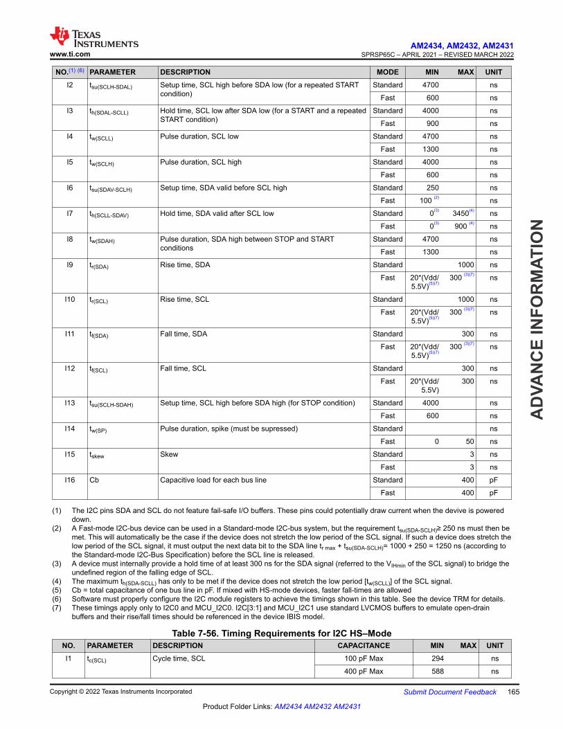
NO.(1) (6) PARAMETER DESCRIPTION MODE MIN MAX UNITI2 tsu(SCLH-SDAL) Setup time, SCL high before SDA low (for a repeated START
condition)Standard 4700 ns
Fast 600 ns
I3 th(SDAL-SCLL) Hold time, SCL low after SDA low (for a START and a repeated START condition)
Standard 4000 ns
Fast 900 ns
I4 tw(SCLL) Pulse duration, SCL low Standard 4700 ns
Fast 1300 ns
I5 tw(SCLH) Pulse duration, SCL high Standard 4000 ns
Fast 600 ns
I6 tsu(SDAV-SCLH) Setup time, SDA valid before SCL high Standard 250 ns
Fast 100 (2) ns
I7 th(SCLL-SDAV) Hold time, SDA valid after SCL low Standard 0(3) 3450(4) ns
Fast 0(3) 900 (4) ns
I8 tw(SDAH) Pulse duration, SDA high between STOP and START conditions
Standard 4700 ns
Fast 1300 ns
I9 tr(SDA) Rise time, SDA Standard 1000 ns
Fast 20*(Vdd/5.5V)(5)(7)
300 (3)(7) ns
I10 tr(SCL) Rise time, SCL Standard 1000 ns
Fast 20*(Vdd/5.5V)(5)(7)
300 (3)(7) ns
I11 tf(SDA) Fall time, SDA Standard 300 ns
Fast 20*(Vdd/5.5V)(5)(7)
300 (3)(7) ns
I12 tf(SCL) Fall time, SCL Standard 300 ns
Fast 20*(Vdd/5.5V)
300 ns
I13 tsu(SCLH-SDAH) Setup time, SCL high before SDA high (for STOP condition) Standard 4000 ns
Fast 600 ns
I14 tw(SP) Pulse duration, spike (must be supressed) Standard ns
Fast 0 50 ns
I15 tskew Skew Standard 3 ns
Fast 3 ns
I16 Cb Capacitive load for each bus line Standard 400 pF
Fast 400 pF
(1) The I2C pins SDA and SCL do not feature fail-safe I/O buffers. These pins could potentially draw current when the devive is powered down.
(2) A Fast-mode I2C-bus device can be used in a Standard-mode I2C-bus system, but the requirement tsu(SDA-SCLH)≥ 250 ns must then be met. This will automatically be the case if the device does not stretch the low period of the SCL signal. If such a device does stretch the low period of the SCL signal, it must output the next data bit to the SDA line tr max + tsu(SDA-SCLH)= 1000 + 250 = 1250 ns (according to the Standard-mode I2C-Bus Specification) before the SCL line is released.
(3) A device must internally provide a hold time of at least 300 ns for the SDA signal (referred to the VIHmin of the SCL signal) to bridge the undefined region of the falling edge of SCL.
(4) The maximum th(SDA-SCLL) has only to be met if the device does not stretch the low period [tw(SCLL)] of the SCL signal.(5) Cb = total capacitance of one bus line in pF. If mixed with HS-mode devices, faster fall-times are allowed(6) Software must properly configure the I2C module registers to achieve the timings shown in this table. See the device TRM for details.(7) These timings apply only to I2C0 and MCU_I2C0. I2C[3:1] and MCU_I2C1 use standard LVCMOS buffers to emulate open-drain
buffers and their rise/fall times should be referenced in the device IBIS model.
Table 7-56. Timing Requirements for I2C HS–ModeNO. PARAMETER DESCRIPTION CAPACITANCE MIN MAX UNITI1 tc(SCL) Cycle time, SCL 100 pF Max 294 ns
400 pF Max 588 ns
www.ti.comAM2434, AM2432, AM2431
SPRSP65C – APRIL 2021 – REVISED MARCH 2022
AD
VAN
CE
INFO
RM
ATIO
N
Copyright © 2022 Texas Instruments Incorporated Submit Document Feedback 165
Product Folder Links: AM2434 AM2432 AM2431

Table 7-56. Timing Requirements for I2C HS–Mode (continued)NO. PARAMETER DESCRIPTION CAPACITANCE MIN MAX UNITI2 tsu(SCLH-SDAL) Setup time, SCL high before SDA low (for a
repeated START condition)100 pF Max 160 ns
400 pF Max 160 ns
I3 th(SDAL-SCLL) Hold time, SCL low after SDA low (for a START and a repeated START condition)
100 pF Max 160 ns
400 pF Max 160 ns
I4 tw(SCLL) Pulse duration, SCL low 100 pF Max 160 ns
400 pF Max 320 ns
I5 tw(SCLH) Pulse duration, SCL high 100 pF Max 60 ns
400 pF Max 120 ns
I6 tsu(SDAV-SCLH) Setup time, SDA valid before SCL high 100 pF Max 10 ns
400 pF Max 10 ns
I7 th(SCLL-SDAV) Hold time, SDA valid after SCL low 100 pF Max 0 70 ns
400 pF Max 0 150 ns
I13 tw(SDAH) Setup time, SCL high before SDA high (for STOP condition)
100 pF Max 160 ns
400 pF Max 160 (2) ns
I14 tr(SDA) Pulse duration, spike (must be suppressed) 100 pF Max 0 10 (2) ns
400 pF Max ns
I15 tskew Skew ns
I16 Cb(1) Capacitive Load for SDA and SCL Lines 100 pF Max 100 pF
400 pF Max 400 pF
(1) For bus line loads Cb between 100 pF and 400 pF the timing parameters must be linearly interpolated.(2) A device must internally provide a Data hold time to bridge the undefined part between VIH and VIL of the falling edge of the SCLH
signal. An input circuit with a threshold as low as possible for the falling edge of the SCLH signal minimizes this hold time.
I10
I8
I4
I3
I7
I12
I5
I6 I14
I2
I3
I13
Stop Start RepeatedStart
Stop
I2C[i]_SDA
I2C[i]_SCL
I1
I11 I9
A. i = 0 to 1 for MCU domaini = 0 to 3 for MAIN domain
Figure 7-52. I2C Receive Timing
7.10.5.10 MCAN
Table 7-57 and Table 7-58 presents timing conditions and switching characteristics for MCAN.
For more details about features and additional description information on the device Controller Area Network Interface, see the corresponding subsections within Signal Descriptions and Detailed Description sections.
AM2434, AM2432, AM2431SPRSP65C – APRIL 2021 – REVISED MARCH 2022 www.ti.com
AD
VAN
CE IN
FOR
MATIO
N
166 Submit Document Feedback Copyright © 2022 Texas Instruments Incorporated
Product Folder Links: AM2434 AM2432 AM2431

Note
The device has multiple MCAN modules. MCANn is a generic prefix applied to MCAN signal names, where n represents the specific MCAN module.
Table 7-57. MCAN Timing ConditionsPARAMETER MIN MAX UNIT
INPUT CONDITIONSSRI Input slew rate 2 15 V/ns
OUTPUT CONDITIONSCL Output load capacitance 5 20 pF
Table 7-58. MCAN Switching CharacteristicsNO. PARAMETER DESCRIPTION MIN MAX UNIT
MCAN1 td(MCAN_TX) Delay time, transmit shift register to MCANn_TX 10 ns
MCAN2 td(MCAN_RX) Delay time, MCANn_RX to receive shift register 10 ns
For more information, see Controller Area Network (MCAN) section in Peripherals chapter in the device TRM.
7.10.5.11 MCSPI
For more details about features and additional description information on the device Serial Port Interface, see the corresponding subsections within Signal Descriptions and Detailed Description sections.
Table 7-59 presents timing conditions for MCSPI.
For more information, see Multichannel Serial Peripheral Interface (MCSPI) section in Peripherals chapter in the device TRM.
Table 7-59. MCSPI Timing ConditionsPARAMETER MIN MAX UNIT
INPUT CONDITIONSSRI Input slew rate 2 8.5 V/ns
OUTPUT CONDITIONSCL Output load capacitance 6 12 pF
7.10.5.11.1 MCSPI — Master Mode
Table 7-60, Figure 7-53, Table 7-61, and Figure 7-54 present timing requirements and switching characteristics for SPI – Master Mode.
Table 7-60. MCSPI Timing Requirements – Master Modesee Figure 7-53
NO. PARAMETER DESCRIPTION MIN MAX UNITSM4 tsu(MISO-SPICLK) Setup time, SPIn_D[x] valid before SPIn_CLK active edge 2.8 ns
SM5 th(SPICLK-MISO) Hold time, SPIn_D[x] valid after SPIn_CLK active edge 3 ns
www.ti.comAM2434, AM2432, AM2431
SPRSP65C – APRIL 2021 – REVISED MARCH 2022
AD
VAN
CE
INFO
RM
ATIO
N
Copyright © 2022 Texas Instruments Incorporated Submit Document Feedback 167
Product Folder Links: AM2434 AM2432 AM2431

SPI_CS[i] (OUT)
SPI_SCLK (OUT)
SPI_SCLK (OUT)
SPI_D[x] (IN)
SPI_CS[i] (OUT)
SPI_SCLK (OUT)
SPI_SCLK (OUT)
SPI_D[x] (IN)
Bit n-1 Bit n-2 Bit n-3 Bit n-4 Bit 0
Bit n-1 Bit n-2 Bit n-3 Bit 1 Bit 0
PHA=0
EPOL=1
PHA=1
EPOL=1
POL=0
POL=1
POL=0
POL=1
SM8 SM9
SM3
SM1
SM2
SM1
SM8 SM9SM3
SM1
SM2
SM1
SM2
SM3
SM2
SM3
SM4
SM5
SM4
SM5
SM4
SM4
SM5
SM5
SPRSP08_TIMING_McSPI_02
Figure 7-53. SPI Master Mode Receive Timing
Table 7-61. MCSPI Switching Characteristics - Master Modesee Figure 7-54
NO. PARAMETER MIN MAX UNIT
SM1 tc(SPICLK) Cycle time, SPIn_CLK 20 ns
SM2 tw(SPICLKL) Pulse duration, SPIn_CLK low 0.5P - 1(1) ns
SM3 tw(SPICLKH) Pulse duration, SPIn_CLK high 0.5P - 1(1) ns
SM6 td(SPICLK-SIMO) Delay time, SPIn_CLK active edge to SPIn_D[x] -3 2.5 ns
SM7 td(CS-SIMO) Delay time, SPIn_CSi active edge to SPIn_D[x] 5 ns
SM8 td(CS-SPICLK) Delay time, SPIn_CSi active to SPIn_CLK first edge PHA = 0 B - 4 (3) ns
PHA = 1 A - 4 (2) ns
SM9 td(SPICLK-CS) Delay time, SPIn_CLK last edge to SPIn_CSi inactive PHA = 0 A - 4(2) ns
PHA = 1 B - 4(3) ns
(1) P = SPI_CLK period in ns.(2) When P = 20.8 ns, A = (TCS + 1) * TSPICLKREF, where TCS is a bit field of the SPI_CH(i)CONF register. When P > 20.8 ns, A =
(TCS + 0.5) * Fratio * TSPICLKREF, where TCS is a bit field of the SPI_CH(i)CONF register.
AM2434, AM2432, AM2431SPRSP65C – APRIL 2021 – REVISED MARCH 2022 www.ti.com
AD
VAN
CE IN
FOR
MATIO
N
168 Submit Document Feedback Copyright © 2022 Texas Instruments Incorporated
Product Folder Links: AM2434 AM2432 AM2431
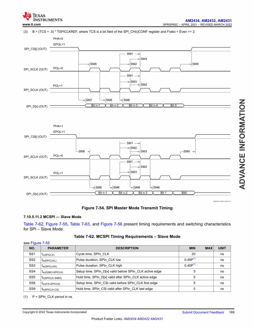
(3) B = (TCS + .5) * TSPICLKREF, where TCS is a bit field of the SPI_CH(i)CONF register and Fratio = Even >= 2.
SPI_CS[i] (OUT)
SPI_SCLK (OUT)
SPI_SCLK (OUT)
SPI_D[x] (OUT)
SPI_CS[i] (OUT)
SPI_SCLK (OUT)
SPI_SCLK (OUT)
SPI_D[x] (OUT)
Bit n-1 Bit n-2 Bit n-3 Bit n-4 Bit 0
Bit n-1 Bit n-2 Bit n-3 Bit 1 Bit0
PHA=0
EPOL=1
POL=0
POL=1
PHA=1
EPOL=1
POL=0
POL=1
SM8 SM9
SM6
SM3
SM1
SM2
SM1
SM8 SM9SM3
SM1
SM2
SM1
SM6
SM7 SM6
SM2
SM3
SM2
SM3
SM6 SM6 SM6
SPRSP08_TIMING_McSPI_01
Figure 7-54. SPI Master Mode Transmit Timing
7.10.5.11.2 MCSPI — Slave Mode
Table 7-62, Figure 7-55, Table 7-63, and Figure 7-56 present timing requirements and switching characteristics for SPI – Slave Mode.
Table 7-62. MCSPI Timing Requirements – Slave Modesee Figure 7-55
NO. PARAMETER DESCRIPTION MIN MAX UNITSS1 tc(SPICLK) Cycle time, SPIn_CLK 20 ns
SS2 tw(SPICLKL) Pulse duration, SPIn_CLK low 0.45P(1) ns
SS3 tw(SPICLKH) Pulse duration, SPIn_CLK high 0.45P(1) ns
SS4 tsu(SIMO-SPICLK) Setup time, SPIn_D[x] valid before SPIn_CLK active edge 5 ns
SS5 th(SPICLK-SIMO) Hold time, SPIn_D[x] valid after SPIn_CLK active edge 5 ns
SS8 tsu(CS-SPICLK) Setup time, SPIn_CSi valid before SPIn_CLK first edge 5 ns
SS9 th(SPICLK-CS) Hold time, SPIn_CSi valid after SPIn_CLK last edge 5 ns
(1) P = SPIn_CLK period in ns.
www.ti.comAM2434, AM2432, AM2431
SPRSP65C – APRIL 2021 – REVISED MARCH 2022
AD
VAN
CE
INFO
RM
ATIO
N
Copyright © 2022 Texas Instruments Incorporated Submit Document Feedback 169
Product Folder Links: AM2434 AM2432 AM2431

SPI_CS[i] (IN)
SPI_SCLK (IN)
SPI_SCLK (IN)
SPI_D[x] (IN)
SPI_CS[i] (IN)
SPI_SCLK (IN)
SPI_SCLK (IN)
SPI_D[x] (IN)
Bit n-1 Bit n-2 Bit n-3 Bit n-4 Bit 0
Bit n-1 Bit n-2 Bit n-3 Bit 1 Bit 0
PHA=0
EPOL=1
POL=0
POL=1
POL=0
POL=1
PHA=1
EPOL=1
SS3
SS1
SS3
SS1
SS3
SS1
SS2
SS1
SS8 SS9
SS8 SS9SS2
SS3
SS2
SS2
SS4
SS5
SS5
SS4
SS4
SS5
SS4
SS5
SPRSP08_TIMING_McSPI_04
Figure 7-55. SPI Slave Mode Receive Timing
Table 7-63. MCSPI Switching Characteristics – Slave Modesee Figure 7-56
NO. PARAMETER DESCRIPTION MIN MAX UNITSS6 td(SPICLK-SOMI) Delay time, SPIn_CLK active edge to SPIn_D[x] 2 17.12 ns
SS7 tsk(CS-SOMI) Delay time, SPIn_CSi active edge to SPIn_D[x] 20.95 ns
AM2434, AM2432, AM2431SPRSP65C – APRIL 2021 – REVISED MARCH 2022 www.ti.com
AD
VAN
CE IN
FOR
MATIO
N
170 Submit Document Feedback Copyright © 2022 Texas Instruments Incorporated
Product Folder Links: AM2434 AM2432 AM2431

SPI_CS[i] (IN)
SPI_SCLK (IN)
SPI_SCLK (IN)
SPI_D[x] (OUT)
SPI_CS[i] (IN)
SPI_SCLK (IN)
SPI_SCLK (IN)
SPI_D[x] (OUT)
Bit n-1 Bit n-2 Bit n-3 Bit n-4 Bit 0
Bit n-1 Bit n-2 Bit n-3 Bit 1 Bit 0
PHA=0
EPOL=1
POL=0
POL=1
POL=0
POL=1
PHA=1
EPOL=1
SS6
SS3
SS1
SS3
SS1
SS3
SS1
SS2
SS1
SS6
SS6
SS8 SS9
SS7
SS8SS2
SS3
SS2
SS2
SS6 SS6SS6
SS9
SPRSP08_TIMING_McSPI_03
Figure 7-56. SPI Slave Mode Transmit Timing
7.10.5.12 MMCSD
The MMCSD Host Controller provides an interface to embedded Multi-Media Card (MMC), Secure Digital (SD), and Secure Digital IO (SDIO) devices. The MMCSD Host Controller deals with MMC/SD/SDIO protocol at transmission level, data packing, adding cyclic redundancy checks (CRCs), start/end bit insertion, and checking for syntactical correctness.
For more details about MMCSD interfaces, see the corresponding MMC0 and MMC1 subsections within Signal Descriptions and Detailed Description sections.
Note
Some operating modes require software configuration of the MMC DLL delay settings, as shown in Table 7-64 and Table 7-73.
For more information, see Multi-Media Card/Secure Digital (MMCSD) Interface section in Peripherals chapter in the device TRM.
www.ti.comAM2434, AM2432, AM2431
SPRSP65C – APRIL 2021 – REVISED MARCH 2022
AD
VAN
CE
INFO
RM
ATIO
N
Copyright © 2022 Texas Instruments Incorporated Submit Document Feedback 171
Product Folder Links: AM2434 AM2432 AM2431

7.10.5.12.1 MMC0 - eMMC Interface
MMC0 interface is compliant with the JEDEC eMMC electrical standard v5.1 (JESD84-B51) and it supports the following eMMC applications:• Legacy speed• High speed SDR• High speed DDR• HS200
Table 7-64 presents the required DLL software configuration settings for MMC0 timing modes.
Table 7-64. MMC0 DLL Delay Mapping for All Timing ModesREGISTER NAME MMCSD0_SS_PHY_CTRL_4_REG MMCSD0_SS_PHY_CTRL_5_REG
BIT FIELD [31:24] [20] [15:12] [8] [4:0] [17:16] [10:8] [2:0]
BIT FIELD NAME STRBSEL OTAPDLYENA OTAPDLYSEL ITAPDLYENA ITAPDLYSEL SELDLYTXCLKSELDLYRXCLK FRQSEL CLKBUFSEL
MODE DESCRIPTION STROBEDELAY
OUTPUTDELAY
ENABLE
OUTPUTDELAYVALUE
INPUTDELAY
ENABLE
INPUTDELAYVALUE
DLLDELAY CHAIN
SELECT
DLL REFFREQUENCY
DELAYBUFFER
DURATION
Legacy SDR
8-bit PHY operating 1.8 V,
25 MHz0x0 0x0 NA 0x1 0x10 0x1 0x0 0x7
High Speed SDR
8-bit PHY operating 1.8 V,
50 MHz0x0 0x0 NA 0x1 0xA 0x1 0x0 0x7
High Speed DDR
8-bit PHY operating 1.8 V,
50 MHz0x0 0x1 0x6 0x1 0x3 0x0 0x4 0x7
HS2008-bit PHY
operating 1.8 V, 200 MHz
0x0 0x1 0x7 0x1 Tuning 0x0 0x0 0x7
Table 7-65 presents timing conditions for MMC0.
Table 7-65. MMC0 Timing ConditionsPARAMETER MIN MAX UNIT
INPUT CONDITIONS
SRI Input slew rate
Legacy SDR 0.14 1.44 V/ns
High Speed SDR 0.3 0.9 V/ns
High Speed DDR (CMD) 0.3 0.9 V/ns
High Speed DDR (DAT[7:0]) 0.45 0.9 V/ns
OUTPUT CONDITIONS
CL Output load capacitance
Legacy SDR 1 12 pF
High Speed SDR 1 12 pF
High Speed DDR 1 12 pF
HS200 1 6 pF
PCB CONNECTIVITY REQUIREMENTStd(Trace Delay) Propagation delay of each trace All modes 126 756 ps
td(Trace Mismatch Delay)
Propagation delay mismatch across all traces
Legacy SDR, High Speed SDR 100 ps
High Speed DDR, HS200 8 ps
AM2434, AM2432, AM2431SPRSP65C – APRIL 2021 – REVISED MARCH 2022 www.ti.com
AD
VAN
CE IN
FOR
MATIO
N
172 Submit Document Feedback Copyright © 2022 Texas Instruments Incorporated
Product Folder Links: AM2434 AM2432 AM2431

7.10.5.12.1.1 Legacy SDR Mode
Table 7-66, Figure 7-57, Table 7-67, and Figure 7-58 present timing requirements and switching characteristics for MMC0 – Legacy SDR Mode.
Table 7-66. MMC0 Timing Requirements – Legacy SDR Modesee Figure 7-57
NO. MIN MAX UNITLSDR1 tsu(cmdV-clkH) Setup time, MMC0_CMD valid before MMC0_CLK rising edge 9.69 ns
LSDR2 th(clkH-cmdV) Hold time, MMC0_CMD valid after MMC0_CLK rising edge 27.97 ns
LSDR3 tsu(dV-clkH) Setup time, MMC0_DAT[7:0] valid before MMC0_CLK rising edge 9.69 ns
LSDR4 th(clkH-dV) Hold time, MMC0_DAT[7:0] valid after MMC0_CLK rising edge 27.97 ns
Figure 7-57. MMC0 – Legacy SDR – Receive Mode
Table 7-67. MMC0 Switching Characteristics – Legacy SDR Modesee Figure 7-58
NO. PARAMETER MIN MAX UNITfop(clk) Operating frequency, MMC0_CLK 25 MHz
LSDR5 tc(clk) Cycle time, MMC0_CLK 40 ns
LSDR6 tw(clkH) Pulse duration, MMC0_CLK high 18.7 ns
LSDR7 tw(clkL) Pulse duration, MMC0_CLK low 18.7 ns
LSDR8 td(clkL-cmdV) Delay time, MMC0_CLK falling edge to MMC0_CMD transition -16.1 16.1 ns
LSDR9 td(clkL-dV) Delay time, MMC0_CLK falling edge to MMC0_DAT[7:0] transition -16.1 16.1 ns
Figure 7-58. MMC0 – Legacy SDR – Transmit Mode
www.ti.comAM2434, AM2432, AM2431
SPRSP65C – APRIL 2021 – REVISED MARCH 2022
AD
VAN
CE
INFO
RM
ATIO
N
Copyright © 2022 Texas Instruments Incorporated Submit Document Feedback 173
Product Folder Links: AM2434 AM2432 AM2431
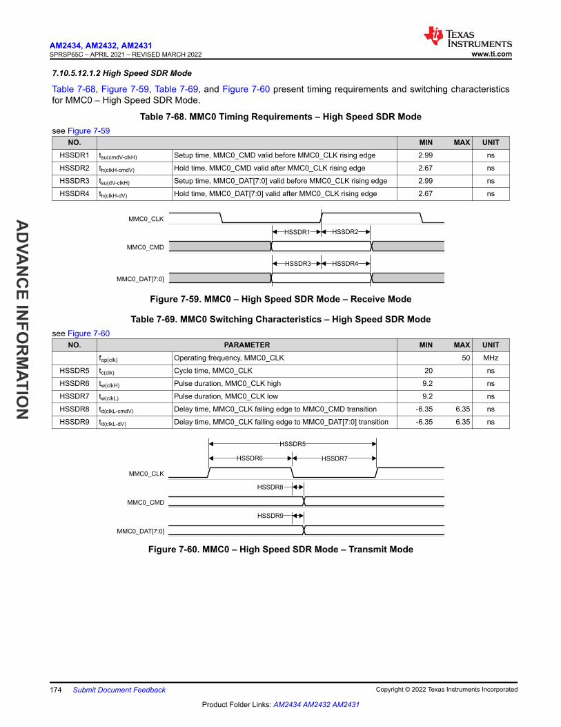
7.10.5.12.1.2 High Speed SDR Mode
Table 7-68, Figure 7-59, Table 7-69, and Figure 7-60 present timing requirements and switching characteristics for MMC0 – High Speed SDR Mode.
Table 7-68. MMC0 Timing Requirements – High Speed SDR Modesee Figure 7-59
NO. MIN MAX UNITHSSDR1 tsu(cmdV-clkH) Setup time, MMC0_CMD valid before MMC0_CLK rising edge 2.99 ns
HSSDR2 th(clkH-cmdV) Hold time, MMC0_CMD valid after MMC0_CLK rising edge 2.67 ns
HSSDR3 tsu(dV-clkH) Setup time, MMC0_DAT[7:0] valid before MMC0_CLK rising edge 2.99 ns
HSSDR4 th(clkH-dV) Hold time, MMC0_DAT[7:0] valid after MMC0_CLK rising edge 2.67 ns
Figure 7-59. MMC0 – High Speed SDR Mode – Receive Mode
Table 7-69. MMC0 Switching Characteristics – High Speed SDR Modesee Figure 7-60
NO. PARAMETER MIN MAX UNITfop(clk) Operating frequency, MMC0_CLK 50 MHz
HSSDR5 tc(clk) Cycle time, MMC0_CLK 20 ns
HSSDR6 tw(clkH) Pulse duration, MMC0_CLK high 9.2 ns
HSSDR7 tw(clkL) Pulse duration, MMC0_CLK low 9.2 ns
HSSDR8 td(clkL-cmdV) Delay time, MMC0_CLK falling edge to MMC0_CMD transition -6.35 6.35 ns
HSSDR9 td(clkL-dV) Delay time, MMC0_CLK falling edge to MMC0_DAT[7:0] transition -6.35 6.35 ns
Figure 7-60. MMC0 – High Speed SDR Mode – Transmit Mode
AM2434, AM2432, AM2431SPRSP65C – APRIL 2021 – REVISED MARCH 2022 www.ti.com
AD
VAN
CE IN
FOR
MATIO
N
174 Submit Document Feedback Copyright © 2022 Texas Instruments Incorporated
Product Folder Links: AM2434 AM2432 AM2431

7.10.5.12.1.3 High Speed DDR Mode
Table 7-70, Figure 7-61, Table 7-71, and Figure 7-62 present timing requirements and switching characteristics for MMC0 – High Speed DDR Mode.
Table 7-70. MMC0 Timing Requirements – High Speed DDR Modesee Figure 7-61
NO. MIN MAX UNITHSDDR1 tsu(cmdV-clk) Setup time, MMC0_CMD valid before MMC0_CLK rising edge 3.88 ns
HSDDR2 th(clk-cmdV) Hold time, MMC0_CMD valid after MMC0_CLK rising edge 2.67 ns
HSDDR3 tsu(dV-clk) Setup time, MMC0_DAT[7:0] valid before MMC0_CLK transition 0.83 ns
HSDDR4 th(clk-dV) Hold time, MMC0_DAT[7:0] valid after MMC0_CLK transition 1.76 ns
Figure 7-61. MMC0 – High Speed DDR Mode – Receive Mode
Table 7-71. MMC0 Switching Characteristics – High Speed DDR Modesee Figure 7-62
NO. PARAMETER MIN MAX UNITfop(clk) Operating frequency, MMC0_CLK 50 MHz
HSDDR5 tc(clk) Cycle time, MMC0_CLK 20 ns
HSDDR6 tw(clkH) Pulse duration, MMC0_CLK high 9.2 ns
HSDDR7 tw(clkL) Pulse duration, MMC0_CLK low 9.2 ns
HSDDR8 td(clk-cmdV) Delay time, MMC0_CLK rising edge to MMC0_CMD transition 3.31 16.19 ns
HSDDR9 td(clk-dV) Delay time, MMC0_CLK transition to MMC0_DAT[7:0] transition 2.81 6.94 ns
Figure 7-62. MMC0 – High Speed DDR Mode – Transmit Mode
www.ti.comAM2434, AM2432, AM2431
SPRSP65C – APRIL 2021 – REVISED MARCH 2022
AD
VAN
CE
INFO
RM
ATIO
N
Copyright © 2022 Texas Instruments Incorporated Submit Document Feedback 175
Product Folder Links: AM2434 AM2432 AM2431

7.10.5.12.1.4 HS200 Mode
Table 7-72 and Figure 7-63 present switching characteristics for MMC0 – HS200 Mode.
Table 7-72. MMC0 Switching Characteristics – HS200 Modesee Figure 7-63
NO. PARAMETER MIN MAX UNITfop(clk) Operating frequency, MMC0_CLK 200 MHz
HS2005 tc(clk) Cycle time, MMC0_CLK 5 ns
HS2006 tw(clkH) Pulse duration, MMC0_CLK high 2.08 ns
HS2007 tw(clkL) Pulse duration, MMC0_CLK low 2.08 ns
HS2008 td(clkL-cmdV) Delay time, MMC0_CLK rising edge to MMC0_CMD transition 0.99 3.28 ns
HS2009 td(clkL-dV) Delay time, MMC0_CLK rising edge to MMC0_DAT[7:0] transition 0.99 3.28 ns
Figure 7-63. MMC0 – HS200 Mode – Transmit Mode
7.10.5.12.2 MMC1 - SD/SDIO Interface
MMC1 interface is compliant with the SD Host Controller Standard Specification 4.10 and SD Physical Layer Specification v3.01 as well as SDIO Specification v3.00 and it supports the following SD Card applications:• Default speed• High speed• UHS–I SDR12• UHS–I SDR25• UHS–I SDR50• UHS–I SDR104• UHS–I DDR50
Table 7-73 presents the required DLL software configuration settings for MMC1 timing modes.
Table 7-73. MMC1 DLL Delay Mapping for All Timing ModesREGISTER NAME MMCSD1_SS_PHY_CTRL_4_REG MMCSD1_SS_PHY_CTRL_5_REG
BIT FIELD [20] [15:12] [8] [4:0] [2:0]BIT FIELD NAME OTAPDLYENA OTAPDLYSEL ITAPDLYENA ITAPDLYSEL CLKBUFSEL
MODE DESCRIPTION DELAYENABLE
DELAYVALUE
INPUTDELAY
ENABLE
INPUTDELAYVALUE
DELAYBUFFER
DURATIONDefaultSpeed
4-bit PHY operating3.3 V, 25 MHz 0x0 0x0 0x1 0x0 0x7
HighSpeed
4-bit PHY operating3.3 V, 50 MHz 0x0 0x0 0x1 0x0 0x7
UHS-ISDR12
4-bit PHY operating1.8 V, 25 MHz 0x1 0xF 0x1 0x0 0x7
UHS-ISDR25
4-bit PHY operating1.8 V, 50 MHz 0x1 0xF 0x1 0x0 0x7
UHS-ISDR50
4-bit PHY operating1.8 V, 100 MHz 0x1 0xC 0x1 Tuning 0x7
AM2434, AM2432, AM2431SPRSP65C – APRIL 2021 – REVISED MARCH 2022 www.ti.com
AD
VAN
CE IN
FOR
MATIO
N
176 Submit Document Feedback Copyright © 2022 Texas Instruments Incorporated
Product Folder Links: AM2434 AM2432 AM2431

Table 7-73. MMC1 DLL Delay Mapping for All Timing Modes (continued)REGISTER NAME MMCSD1_SS_PHY_CTRL_4_REG MMCSD1_SS_PHY_CTRL_5_REG
BIT FIELD [20] [15:12] [8] [4:0] [2:0]BIT FIELD NAME OTAPDLYENA OTAPDLYSEL ITAPDLYENA ITAPDLYSEL CLKBUFSEL
MODE DESCRIPTION DELAYENABLE
DELAYVALUE
INPUTDELAY
ENABLE
INPUTDELAYVALUE
DELAYBUFFER
DURATIONUHS-IDR50
4-bit PHY operating1.8 V, 50 MHz 0x1 0x9 0x1 Tuning 0x7
UHS-ISDR104
4-bit PHY operating1.8, V 200 MHz 0x1 0x6 0x1 Tuning 0x7
Table 7-74 presents timing conditions for MMC1.
Table 7-74. MMC1 Timing ConditionsPARAMETER MIN MAX UNIT
Input Conditions
SRI Input slew rate
Default Speed, High Speed 0.69 2.06 V/ns
UHS–I SDR12, UHS–I SDR25 0.34 1.34 V/ns
UHS–I DDR50 1 2 V/ns
Output Conditions
CL Output load capacitanceUHS–I DDR50 3 10 pF
All other modes 1 10 pF
PCB Connectivity Requirements
td(Trace Delay) Propagation delay of each traceUHS–I DDR50 240 1134 ps
All other modes 126 1386 ps
td(Trace Mismatch Delay)
Propagation delay mismatch across all traces
UHS–I DDR50, UHS–I SDR104 20 ps
All other modes 100 ps
www.ti.comAM2434, AM2432, AM2431
SPRSP65C – APRIL 2021 – REVISED MARCH 2022
AD
VAN
CE
INFO
RM
ATIO
N
Copyright © 2022 Texas Instruments Incorporated Submit Document Feedback 177
Product Folder Links: AM2434 AM2432 AM2431

7.10.5.12.2.1 Default Speed Mode
Table 7-75, Figure 7-64, Table 7-76, and Figure 7-65 present timing requirements and switching characteristics for MMC1 – Default Speed Mode.
Table 7-75. Timing Requirements for MMC1 – Default Speed Modesee Figure 7-64
NO. MIN MAX UNITDS1 tsu(cmdV-clkH) Setup time, MMC1_CMD valid before MMCi_CLK rising edge 2.55 ns
DS2 th(clkH-cmdV) Hold time, MMC1_CMD valid after MMC1_CLK rising edge 19.67 ns
DS3 tsu(dV-clkH) Setup time, MMC1_DAT[3:0] valid before MMC1_CLK rising edge 2.55 ns
DS4 th(clkH-dV) Hold time, MMC1_DAT[3:0] valid after MMC1_CLK rising edge 19.67 ns
MMC[ ]_CLKx
M [ ]_MC CMDx
MMC DAT[ ]_ [3:0]x
DS1 DS2
DS3 DS4
Figure 7-64. MMC1 – Default Speed – Receive Mode
Table 7-76. Switching Characteristics for MMC1 – Default Speed Modesee Figure 7-65
NO. PARAMETER MIN MAX UNITfop(clk) Operating frequency, MMC1_CLK 25 MHz
DS5 tc(clk) Cycle time, MMC1_CLK 40 ns
DS6 tw(clkH) Pulse duration, MMC1_CLK high 18.7 ns
DS7 tw(clkL) Pulse duration, MMC1_CLK low 18.7 ns
DS8 td(clkL-cmdV) Delay time, MMC1_CLK falling edge to MMC1_CMD transition - 14.1 14.1 ns
DS9 td(clkL-dV) Delay time, MMC1_CLK falling edge to MMC1_DAT[3:0] transition - 14.1 14.1 ns
MMC[ ]_CLKx
MMC CMD[ ]_x
MMC DAT[ _ [3:0]x]
D 5S
D 7S
D 8S
D 9S
DS6
Figure 7-65. MMC1 – Default Speed – Transmit Mode
AM2434, AM2432, AM2431SPRSP65C – APRIL 2021 – REVISED MARCH 2022 www.ti.com
AD
VAN
CE IN
FOR
MATIO
N
178 Submit Document Feedback Copyright © 2022 Texas Instruments Incorporated
Product Folder Links: AM2434 AM2432 AM2431

7.10.5.12.2.2 High Speed Mode
Table 7-77, Figure 7-66, Table 7-78, and Figure 7-67 present timing requirements and switching characteristics for MMC1 – High Speed Mode.
Table 7-77. Timing Requirements for MMC1 – High Speed Modesee Figure 7-66
NO. MIN MAX UNITHS1 tsu(cmdV-clkH) Setup time, MMC1_CMD valid before MMC1_CLK rising edge 2.55 ns
HS2 th(clkH-cmdV) Hold time, MMC1_CMD valid after MMC1_CLK rising edge 2.67 ns
HS3 tsu(dV-clkH) Setup time, MMC1_DAT[3:0] valid before MMC1_CLK rising edge 2.55 ns
HS4 th(clkH-dV) Hold time, MMC1_DAT[3:0] valid after MMC1_CLK rising edge 2.67 ns
MMC[ ]_CLKx
MMC[ ]_CMDx
MMC DAT[ ]_ [3:0]x
H 1S H 2S
H 3S H 4S
Figure 7-66. MMC1 – High Speed – Receive Mode
Table 7-78. Switching Characteristics for MMC1 – High Speed Modesee Figure 7-67
NO. PARAMETER MIN MAX UNITfop(clk) Operating frequency, MMC1_CLK 50 MHz
HS5 tc(clk) Cycle time. MMC1_CLK 20 ns
HS6 tw(clkH) Pulse duration, MMC1_CLK high 9.2 ns
HS7 tw(clkL) Pulse duration, MMC1_CLK low 9.2 ns
HS8 td(clkL-cmdV) Delay time, MMC1_CLK falling edge to MMC1_CMD transition -7.35 3.35 ns
HS9 td(clkL-dV) Delay time, MMC1_CLK falling edge to MMC1_DAT[3:0] transition -7.35 3.35 ns
MMC[x]_CLK
MMC CMD[ ]_x
MMC DAT[ ]_ [3:0]x
H 5S
H 7S
H 8S
H 9S
HS6
Figure 7-67. MMC1 – High Speed – Transmit Mode
www.ti.comAM2434, AM2432, AM2431
SPRSP65C – APRIL 2021 – REVISED MARCH 2022
AD
VAN
CE
INFO
RM
ATIO
N
Copyright © 2022 Texas Instruments Incorporated Submit Document Feedback 179
Product Folder Links: AM2434 AM2432 AM2431

7.10.5.12.2.3 UHS–I SDR12 Mode
Table 7-79, Figure 7-68, Table 7-80, and Figure 7-69 present timing requirements and switching characteristics for MMC1 – UHS-I SDR12 Mode.
Table 7-79. Timing Requirements for MMC1 – UHS-I SDR12 Modesee Figure 7-68
NO. MIN MAX UNITSDR121 tsu(cmdV-clkH) Setup time, MMC1_CMD valid before MMC1_CLK rising edge 21.65 ns
SDR122 th(clkH-cmdV) Hold time, MMC1_CMD valid after MMC1_CLK rising edge 1.67 ns
SDR123 tsu(dV-clkH) Setup time, MMC1_DAT[3:0] valid before MMC1_CLK rising edge 21.65 ns
SDR124 th(clkH-dV) Hold time, MMC1_DAT[3:0] valid after MMC1_CLK rising edge 1.67 ns
MMC[ ]_CMDx
MMC DAT[ ]_ [3:0]x
SDR121 SDR122
SDR123 SDR124
MMC[ ]_CLKx
Figure 7-68. MMC1 – UHS-I SDR12 – Receive Mode
Table 7-80. Switching Characteristics for MMC1 – UHS-I SDR12 Modesee Figure 7-69
NO. PARAMETER MIN MAX UNITfop(clk) Operating frequency, MMC1_CLK 25 MHz
SDR125 tc(clk) Cycle time, MMC1_CLK 40 ns
SDR126 tw(clkH) Pulse duration, MMC1_CLK high 18.7 ns
SDR127 tw(clkL) Pulse duration, MMC1_CLK low 18.7 ns
SDR128 td(clkL-cmdV) Delay time, MMC1_CLK falling edge to MMC1_CMD transition -13.6 13.6 ns
SDR129 td(clkL-dV) Delay time, MMC1_CLK falling edge to MMC1_DAT[3:0] transition -13.6 13.6 ns
MMC[ ]_CLKx
MMC CMD[ ]_x
MMC DAT[ ]_ [3:0]x
SDR125
SDR127SDR126
SDR128
SDR129
SDR128
SDR129
Figure 7-69. MMC1 – UHS-I SDR12 – Transmit Mode
AM2434, AM2432, AM2431SPRSP65C – APRIL 2021 – REVISED MARCH 2022 www.ti.com
AD
VAN
CE IN
FOR
MATIO
N
180 Submit Document Feedback Copyright © 2022 Texas Instruments Incorporated
Product Folder Links: AM2434 AM2432 AM2431
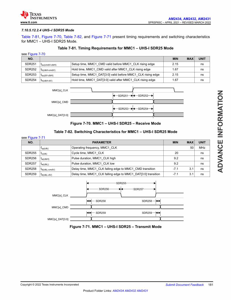
7.10.5.12.2.4 UHS–I SDR25 Mode
Table 7-81, Figure 7-70, Table 7-82, and Figure 7-71 present timing requirements and switching characteristics for MMC1 – UHS-I SDR25 Mode.
Table 7-81. Timing Requirements for MMC1 – UHS-I SDR25 Modesee Figure 7-70
NO. MIN MAX UNITSDR251 tsu(cmdV-clkH) Setup time, MMC1_CMD valid before MMC1_CLK rising edge 2.15 ns
SDR252 th(clkH-cmdV) Hold time, MMC1_CMD valid after MMC1_CLK rising edge 1.67 ns
SDR253 tsu(dV-clkH) Setup time, MMC1_DAT[3:0] valid before MMC1_CLK rising edge 2.15 ns
SDR254 th(clkH-dV) Hold time, MMC1_DAT[3:0] valid after MMC1_CLK rising edge 1.67 ns
MMC[ ]_CLKx
MMC[ ]_CMDx
MMC DAT[ ]_ [3:0]x
SDR251 SDR252
SDR253 SDR254
Figure 7-70. MMC1 – UHS-I SDR25 – Receive Mode
Table 7-82. Switching Characteristics for MMC1 – UHS-I SDR25 Modesee Figure 7-71
NO. PARAMETER MIN MAX UNITfop(clk) Operating frequency, MMC1_CLK 50 MHz
SDR255 tc(clk) Cycle time, MMC1_CLK 20 ns
SDR256 tw(clkH) Pulse duration, MMC1_CLK high 9.2 ns
SDR257 tw(clkL) Pulse duration, MMC1_CLK low 9.2 ns
SDR258 td(clkL-cmdV) Delay time, MMC1_CLK falling edge to MMC1_CMD transition -7.1 3.1 ns
SDR259 td(clkL-dV) Delay time, MMC1_CLK falling edge to MMC1_DAT[3:0] transition -7.1 3.1 ns
MMC[ ]_CLKx
MMC CMD[ ]_x
MMC DAT[ _ [3:0]x]
SDR255
SDR257SDR256
SDR258
SDR259
SDR258
SDR259
Figure 7-71. MMC1 – UHS-I SDR25 – Transmit Mode
www.ti.comAM2434, AM2432, AM2431
SPRSP65C – APRIL 2021 – REVISED MARCH 2022
AD
VAN
CE
INFO
RM
ATIO
N
Copyright © 2022 Texas Instruments Incorporated Submit Document Feedback 181
Product Folder Links: AM2434 AM2432 AM2431
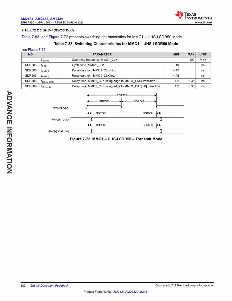
7.10.5.12.2.5 UHS–I SDR50 Mode
Table 7-83, and Figure 7-72 presents switching characteristics for MMC1 – UHS-I SDR50 Mode.
Table 7-83. Switching Characteristics for MMC1 – UHS-I SDR50 Modesee Figure 7-72
NO. PARAMETER MIN MAX UNITfop(clk) Operating frequency, MMC1_CLK 100 MHz
SDR505 tc(clk) Cycle time, MMC1_CLK 10 ns
SDR506 tw(clkH) Pulse duration, MMC1_CLK high 4.45 ns
SDR507 tw(clkL) Pulse duration, MMC1_CLK low 4.45 ns
SDR508 td(clkL-cmdV) Delay time, MMC1_CLK rising edge to MMC1_CMD transition 1.2 6.35 ns
SDR509 td(clkL-dV) Delay time, MMC1_CLK rising edge to MMC1_DAT[3:0] transition 1.2 6.35 ns
MMC[ ]_CLKx
MMC CMD[ ]_x
MMC DAT[x]_ [3:0]
SDR505
SDR507SDR506
SDR508
SDR509
SDR508
SDR509
Figure 7-72. MMC1 – UHS-I SDR50 – Transmit Mode
AM2434, AM2432, AM2431SPRSP65C – APRIL 2021 – REVISED MARCH 2022 www.ti.com
AD
VAN
CE IN
FOR
MATIO
N
182 Submit Document Feedback Copyright © 2022 Texas Instruments Incorporated
Product Folder Links: AM2434 AM2432 AM2431

7.10.5.12.2.6 UHS–I DDR50 Mode
Table 7-84, Figure 7-73, Table 7-85, and Figure 7-74 present timing requirements and switching characteristics for MMC1 – UHS-I DDR50 Mode.
Table 7-84. Timing Requirements for MMC1 – UHS-I DDR50 Modesee Figure 7-73
NO. MIN MAX UNITDDR501 tsu(cmdV-clk) Setup time, MMC1_CMD valid before MMC1_CLK rising edge 2.99 ns
DDR502 th(clk-cmdV) Hold time, MMC1_CMD valid after MMC1_CLK rising edge 1.91 ns
DDR503 tsu(dV-clk) Setup time, MMC1_DAT[3:0] valid before MMC1_CLK transition -0.06 ns
DDR504 th(clk-dV) Hold time, MMC1_DAT[3:0] valid after MMC1_CLK transition 1.91 ns
MMC[x] CLK_
MMC[x] CMD_
MMC[x] DAT 3_ [ :0]
DDR501 DDR502
DDR504
DDR503 DDR503
DDR504
Figure 7-73. MMC1 – UHS-I DDR50 – Receive Mode
Table 7-85. Switching Characteristics for MMC1 – UHS-I DDR50 Modesee Figure 7-74
NO. PARAMETER MIN MAX UNITfop(clk) Operating frequency, MMC1_CLK 50 MHz
DDR505 tc(clk) Cycle time, MMC1_CLK 20 ns
DDR506 tw(clkH) Pulse duration, MMC1_CLK high 9.2 ns
DDR507 tw(clkL) Pulse duration, MMC1_CLK low 9.2 ns
DDR508 td(clk-cmdV) Delay time, MMC1_CLK rising edge to MMC1_CMD transition 1.2 13.1 ns
DDR509 td(clk-dV) Delay time, MMC1_CLK transition to MMC1_DAT[3:0] transition 1.2 6.35 ns
MMC[x] CLK_
MMC[x] CMD_
MMC[x] DAT 3_ [ :0]
DDR508
DDR509 DDR509
DDR505
DDR506 DDR507
Figure 7-74. MMC1 – UHS-I DDR50 – Transmit Mode
www.ti.comAM2434, AM2432, AM2431
SPRSP65C – APRIL 2021 – REVISED MARCH 2022
AD
VAN
CE
INFO
RM
ATIO
N
Copyright © 2022 Texas Instruments Incorporated Submit Document Feedback 183
Product Folder Links: AM2434 AM2432 AM2431

7.10.5.12.2.7 UHS–I SDR104 Mode
Table 7-86, and Figure 7-75 present switching characteristics for MMC1 – UHS-I SDR104 Mode.
Table 7-86. Switching Characteristics for MMC1 – UHS-I SDR104 Modesee Figure 7-75
NO. PARAMETER MIN MAX UNITfop(clk) Operating frequency, MMC1_CLK 200 MHz
SDR1045 tc(clk) Cycle time, MMC1_CLK 5 ns
SDR1046 tw(clkH) Pulse duration, MMC1_CLK high 2.08 ns
SDR1047 tw(clkL) Pulse duration, MMC1_CLK low 2.08 ns
SDR1048 td(clkL-cmdV) Delay time, MMC1_CLK rising edge to MMC1_CMD transition 1.12 3.16 ns
SDR1049 td(clkL-dV) Delay time, MMC1_CLK rising edge to MMC1_DAT[3:0] transition 1.12 3.16 ns
MMC[ ]_CLKx
MMC CMD[ ]_x
MMC DAT[ ]_ [3:0]x
SDR1045
SDR1047SDR1046
SDR1048
SDR1049
SDR1048
SDR1049
Figure 7-75. MMC1 – UHS-I SDR104 – Transmit Mode
7.10.5.13 CPTS
Table 7-87, Table 7-88, Figure 7-76, Table 7-89, and Figure 7-77 present timing conditions, requirements, and switching characteristics for CPTS.
Table 7-87. CPTS Timing ConditionsPARAMETER MIN MAX UNIT
INPUT CONDITIONSSRI Input slew rate 0.5 5 V/ns
OUTPUT CONDITIONSCL Output load capacitance 2 10 pF
Table 7-88. CPTS Timing Requirementssee Figure 7-76
NO. PARAMETER DESCRIPTION MIN MAX UNITT1 tw(HWTSPUSHH) Pulse duration, HWnTSPUSH high 12P(1) + 2 ns
T2 tw(HWTSPUSHL) Pulse duration, HWnTSPUSH low 12P(1) + 2 ns
T3 tc(RFT_CLK) Cycle time, RFT_CLK 5 8 ns
T4 tw(RFT_CLKH) Pulse duration, RFT_CLK high 0.45T(2) ns
T5 tw(RFT_CLKL) Pulse duration, RFT_CLK low 0.45T(2) ns
(1) P = functional clock period in ns.(2) T = RFT_CLK period in ns.
AM2434, AM2432, AM2431SPRSP65C – APRIL 2021 – REVISED MARCH 2022 www.ti.com
AD
VAN
CE IN
FOR
MATIO
N
184 Submit Document Feedback Copyright © 2022 Texas Instruments Incorporated
Product Folder Links: AM2434 AM2432 AM2431

RFT_CLKT3 T4 T5
HWn_TSPUSH
T1 T2
Figure 7-76. CPTS Timing Requirements
Table 7-89. CPTS Switching Characteristicssee Figure 7-77
NO. PARAMETER DESCRIPTION SOURCE MIN MAX UNITT6 tw(TS_COMPH) Pulse duration, TS_COMP high 36P(1) - 2 ns
T7 tw(TS_COMPL) Pulse duration, TS_COMP low 36P(1) - 2 ns
T8 tw(TS_SYNCH) Pulse duration, TS_SYNC high 36P(1) - 2 ns
T9 tw(TS_SYNCL) Pulse duration, TS_SYNC low 36P(1) - 2 ns
T10 tw(SYNC_OUTH) Pulse duration, SYNCn_OUT high TS_SYNC 36P(1) - 2 ns
GENF 5P(1) - 2 ns
T11 tw(SYNC_OUTL) Pulse duration, SYNCn_OUT low TS_SYNC 36P(1) - 2 ns
GENF 5P(1) - 2 ns
(1) P = functional clock period in ns.
TS_COMP
T6 T7
TS_SYNC
T8 T9
SYNCn_OUT
T10 T11
Figure 7-77. CPTS Switching Characteristics
For more information, see Data Movement Architecture (DMA) chapter in the device TRM.
7.10.5.14 OSPI
For more details about features and additional description information on the device Octal Serial Peripheral Interface, see the corresponding subsections within Signal Descriptions and Detailed Description sections.
Table 7-90 presents timing conditions for OSPI.
Table 7-90. OSPI Timing ConditionsPARAMETER MIN MAX UNIT
INPUT CONDITIONSSRI Input slew rate 1 6 V/ns
OUTPUT CONDITIONSCL Output load capacitance 3 10 pF
PCB CONNECTIVITY REQUIREMENTStd(Trace Delay) Propagation delay of each trace 450 ps
www.ti.comAM2434, AM2432, AM2431
SPRSP65C – APRIL 2021 – REVISED MARCH 2022
AD
VAN
CE
INFO
RM
ATIO
N
Copyright © 2022 Texas Instruments Incorporated Submit Document Feedback 185
Product Folder Links: AM2434 AM2432 AM2431

Table 7-90. OSPI Timing Conditions (continued)PARAMETER MIN MAX UNIT
td(Trace Mismatch Delay)
Propagation delay mismatch across all traces 60 ps
For more information, see Octal Serial Peripheral Interface (OSPI) section in Peripherals chapter in the device TRM.
7.10.5.14.1 OSPI With Data Training7.10.5.14.1.1 OSPI Switching Characteristics – Data Training
Table 7-91 presents switching characteristics for OSPI with Data Training.
Table 7-91. OSPI Switching Characteristics – Data TrainingPARAMETER MODE MIN MAX UNIT
tc(CLK) Cycle time, CLK
1.8V, SDR 6.02 ns
3.3V, SDR 7.52 ns
1.8V, DDR 6.02 ns
3.3V, DDR 7.52 ns
7.10.5.14.2 OSPI Without Data Training
Note
The I/O Timings provided in this section are only applicable when data training is not implemented. Additionally, the I/O Timings are valid only for some OSPI usage modes when the corresponding DLL Delays are configured as described in Table 7-92.
Table 7-92. OSPI DLL Delay Mapping for Timing ModesMODE OSPI_PHY_CONFIGURATION_REG BIT FIELD DELAY VALUE1.8V, OSPI0 DDR TX PHY_CONFIG_TX_DLL_DELAY_FLD 0x45
3.3V, OSPI0 DDR TX PHY_CONFIG_TX_DLL_DELAY_FLD 0x46
1.8V, OSPI0 DQS PHY_CONFIG_RX_DLL_DELAY_FLD 0x14
3.3V, OSPI0 DQS PHY_CONFIG_RX_DLL_DELAY_FLD 0x3A
All other modes PHY_CONFIG_TX_DLL_DELAY_FLD,PHY_CONFIG_RX_DLL_DELAY_FLD
0x0
7.10.5.14.2.1 OSPI SDR Timing
Table 7-93, Figure 7-78, Figure 7-79, Table 7-94, and Figure 7-80 present timing requirements and switching characteristics for OSPI SDR Mode.
Table 7-93. OSPI Timing Requirements – SDR Modesee Figure 7-78 and Figure 7-79
NO.(1) MODE MIN MAX UNIT
O19 tsu(D-CLK)Setup time, D[i:0] valid before active CLK edge
1.8V, No Loopback -2.19 ns
3.3V, No Loopback -1.71 ns
O20 th(CLK-D) Hold time, D[i:0] valid after active CLK edge1.8V, No Loopback 7.62 ns
3.3V, No Loopback 8.1 ns
O21 tsu(D-LBCLK)Setup time, D[i:0] valid before active LBCLK input (DQS) edge
1.8V, External Board Loopback -3.1 ns
3.3V, External Board Loopback -3.47 ns
AM2434, AM2432, AM2431SPRSP65C – APRIL 2021 – REVISED MARCH 2022 www.ti.com
AD
VAN
CE IN
FOR
MATIO
N
186 Submit Document Feedback Copyright © 2022 Texas Instruments Incorporated
Product Folder Links: AM2434 AM2432 AM2431

Table 7-93. OSPI Timing Requirements – SDR Mode (continued)see Figure 7-78 and Figure 7-79
NO.(1) MODE MIN MAX UNIT
O22 th(LBCLK-D)Hold time, D[i:0] valid after active LBCLK input (DQS) edge
1.8V, External Board Loopback 3.31 ns
3.3V, External Board Loopback 4.33 ns
(1) i in [i:0] = 7 for OSPI0
OSPI_CLK
OSPI_D[i:0]
OSPI_TIMING_05
O 91 O20
Figure 7-78. OSPI Timing Requirements – SDR, No Loopback Clock and Internal Pad Loopback Clock
OSPI_DQS
OSPI_TIMING_06
O21 O 22
OSPI_D[i:0]
Figure 7-79. OSPI Timing Requirements – SDR, External Loopback Clock
Table 7-94. OSPI Switching Characteristics – SDR Modesee Figure 7-80NO.(1) PARAMETER MODE MIN MAX UNIT
O7 tc(CLK) Cycle time, CLK1.8V 7 ns
3.3V 6.03 ns
O8 tw(CLKL) Pulse duration, CLK low 0.475P - 0.3 (2) ns
O9 tw(CLKH) Pulse duration, CLK high 0.475P - 0.3 (2) ns
O10 td(CLK-CSn) Delay time, CLK rising edge to CSn active edge- 0.475P –
0.975(N)(R) - 1 (2) (3) (4)
- 0.475P – 0.975(N)(R) +
1 (2) (3) (4)ns
O11 td(CLK-CSn)Delay time, CLK rising edge to CSn inactive edge
0.475P + 0.975(N)(R) -
1 (2) (3) (4)
0.475P + 0.975(N)(R) +
1 (2) (3) (4)ns
O12 td(CLK-D) Delay time, CLK active edge to D[i:0] transition1.8V -1.16 1.25 ns
3.3V -1.33 1.51 ns
(1) i in [i:0] = 7 for OSPI0(2) P = CLK cycle time = SCLK period in ns(3) N = OSPI_DEV_DELAY_REG[D_INIT_FLD](4) R = refclk cycle time in ns
www.ti.comAM2434, AM2432, AM2431
SPRSP65C – APRIL 2021 – REVISED MARCH 2022
AD
VAN
CE
INFO
RM
ATIO
N
Copyright © 2022 Texas Instruments Incorporated Submit Document Feedback 187
Product Folder Links: AM2434 AM2432 AM2431

OSPI_CLK
OSPI_TIMING_02
OSPI_CSn
O10 O11
O9 O8
O12
O7
OSPI_D[i:0]
Figure 7-80. OSPI Switching Characteristics – SDR
7.10.5.14.2.2 OSPI DDR Timing
Table 7-95, Figure 7-81, Figure 7-82, Table 7-96, and Figure 7-83 present timing requirements and switching characteristics for OSPI DDR Mode.
Table 7-95. OSPI Timing Requirements – DDR Modesee Figure 7-81 and Figure 7-82
NO.(1) MODE MIN MAX UNIT
O13 tsu(D-CLK) Setup time, D[i:0] valid before active CLK edge
1.8V, No Loopback or Internal Pad Loopback 5.23 ns
3.3V, No Loopback or Internal Pad Loopback 5.44 ns
O14 th(CLK-D) Hold time, D[i:0] valid after active CLK edge
1.8V, No Loopback or Internal Pad Loopback 1.34 ns
3.3V, No Loopback or Internal Pad Loopback 1.44 ns
O15 tsu(D-LBCLK)Setup time, D[i:0] valid before active LBCLK (DQS) edge
1.8V, External Board Loopback TBD ns
3.3V, External Board Loopback TBD ns
O16 th(LBCLK-D)Hold time, D[i:0] valid after active LBCLK (DQS) edge
1.8V, External Board Loopback TBD (2) ns
3.3V, External Board Loopback TBD (2) ns
O17 tsu(D-DQS) Setup time, D[i:0] valid before active DQS edge1.8V, DQS -0.46 ns
3.3V, DQS -0.66 ns
O18 th(DQS-D) Hold time, D[i:0] valid after active DQS edge1.8V, DQS 3.59 ns
3.3V, DQS 7.92 ns
(1) i in [i:0] = 7 for OSPI0(2) This Hold time requirement is larger than the Hold time provided by a typical flash device. Therefore, the trace length between the SoC
and flash device must be sufficiently long enough to ensure that the Hold time is met at the SoC. The length of the SoC's external loopback clock (OSPI_LBCLKO to OSPI_DQS) may need to be shortened to compensate.
OSPI_CLK
O14O13
OSPI_TIMING_03
OSPI_D[i:0]
Figure 7-81. OSPI Timing Requirements – DDR, No Loopback Clock and Internal Pad Loopback Clock
AM2434, AM2432, AM2431SPRSP65C – APRIL 2021 – REVISED MARCH 2022 www.ti.com
AD
VAN
CE IN
FOR
MATIO
N
188 Submit Document Feedback Copyright © 2022 Texas Instruments Incorporated
Product Folder Links: AM2434 AM2432 AM2431

OSPI_DQS
O16O15
OSPI_TIMING_04
OSPI_D[i:0]
Figure 7-82. OSPI Timing Requirements – DDR, External Loopback Clock and DQS
Table 7-96. OSPI Switching Characteristics – DDR Modesee Figure 7-83NO.(1) PARAMETER MODE MIN MAX UNIT
O1 tc(CLK) Cycle time, CLK 19 ns
O2 tw(CLKL) Pulse duration, CLK low 0.475P - 0.3 (2) ns
O3 tw(CLKH) Pulse duration, CLK high 0.475P - 0.3 (2) ns
O4 td(CLK-CSn) Delay time, CLK rising edge to CSn active edge-0.475P –
0.975(N)(R) - 7 (2) (3) (4)
-0.475P – 0.975(N)(R)
(2) (3) (4)ns
O5 td(CLK-CSn)Delay time, CLK rising edge to CSn inactive edge
0.475P + 0.975(N)(R)
(2) (3) (4)
0.475P + 0.975(N)(R)
(2) (3) (4)ns
O6 td(CLK-D) Delay time, CLK active edge to D[i:0] transition1.8V -7.71 -1.56 ns
3.3V -7.71 -1.56 ns
(1) i in [i:0] = 7 for OSPI0(2) P = CLK cycle time = SCLK period in ns(3) N = OSPI_DEV_DELAY_REG[D_INIT_FLD](4) R = refclk cycle time in ns
OSPI_CLK
OSPI_TIMING_01
OSPI_CSn
O6 O6
O4 O3
O2
O1
O5
OSPI_D[i:0]
Figure 7-83. OSPI Switching Characteristics – DDR
7.10.5.15 PCIe
The PCI-Express Subsystem is compliant with the PCIe® Base Specification, Revision 4.0. Refer to the specification for timing details.
For more details about features and additional description information on the device Peripheral Component Interconnect Express, see the corresponding subsections within Signal Descriptions and Detailed Description sections.
For more information, see Peripheral Component Interconnect Express (PCIe) Subsystem section in Peripherals chapter in the device TRM.
www.ti.comAM2434, AM2432, AM2431
SPRSP65C – APRIL 2021 – REVISED MARCH 2022
AD
VAN
CE
INFO
RM
ATIO
N
Copyright © 2022 Texas Instruments Incorporated Submit Document Feedback 189
Product Folder Links: AM2434 AM2432 AM2431

7.10.5.16 PRU_ICSSG
The device has integrated two identical Programmable Real-Time Unit Subsystem and Industrial Communication Subsystems - Gigabit (PRU_ICSSG), PRU_ICSSG0 and PRU_ICSSG1. The programmable nature of the PRU cores, along with their access to pins, events and all device resources, provides flexibility in implementing fast real-time responses, specialized data handling operations, custom peripheral interfaces, and in offloading tasks from the other processor cores in the device.
For more details about features and additional description information on the device PRU_ICSSG, see the corresponding subsections within Signal Descriptions and Detailed Description sections.
Note
The PRU_ICSSG0 and PRU_ICSSG1 support an internal wrapper multiplexing that expands the device top-level multiplexing.
7.10.5.16.1 PRU_ICSSG Programmable Real-Time Unit (PRU)
Note
The PRU_ICSSG PRU signals have different functionality depending on the mode of operation. The signal naming in this section matches the naming used in the PRU Module Interface section in the device TRM.
Table 7-97. PRU_ICSSG PRU Timing ConditionsPARAMETER MIN MAX UNIT
INPUT CONDITIONSSRI Input slew rate 1 3 V/ns
OUTPUT CONDITIONSCL Output load capacitance 2 30 pF
7.10.5.16.1.1 PRU_ICSSG PRU Direct Output Mode Timing
Table 7-98. PRU_ICSSG PRU Switching Characteristics – Direct Output Modesee Figure 7-84
NO. PARAMETER DESCRIPTION MIN MAX UNITPRDO1 tsk(GPO-GPO) Skew, GPO to GPO 3 ns
GPO[n:0]
PRDO1PRU_TIMING_02
A. n in GPO[n:0] = 19.
Figure 7-84. PRU_ICSSG PRU Direct Output Timing
7.10.5.16.1.2 PRU_ICSSG PRU Parallel Capture Mode Timing
Table 7-99. PRU_ICSSG PRU Timing Requirements – Parallel Capture Modesee Figure 7-85 and Figure 7-86
NO. PARAMETER DESCRIPTION MIN MAX UNITPRPC1 tc(CLOCK) Cycle time, CLOCKIN 20 ns
PRPC2 tw(CLOCKL) Pulse duration, CLOCKIN low 10 ns
PRPC3 tw(CLOCKH) Pulse duration, CLOCKIN high 10 ns
PRPC4 tsu(DATAIN-CLOCK) Setup time, DATAIN valid before CLOCKIN active edge 4 ns
AM2434, AM2432, AM2431SPRSP65C – APRIL 2021 – REVISED MARCH 2022 www.ti.com
AD
VAN
CE IN
FOR
MATIO
N
190 Submit Document Feedback Copyright © 2022 Texas Instruments Incorporated
Product Folder Links: AM2434 AM2432 AM2431

Table 7-99. PRU_ICSSG PRU Timing Requirements – Parallel Capture Mode (continued)see Figure 7-85 and Figure 7-86
NO. PARAMETER DESCRIPTION MIN MAX UNITPRPC5 th(CLOCK-DATAIN) Hold time, DATAIN valid after CLOCKIN active edge 0 ns
CLOCKIN
DATAIN
PRPC1PRPC3
PRPC2
PRPC4
PRPC5
PRU_TIMING_03
Figure 7-85. PRU_ICSSG PRU Parallel Capture Timing Requirements – Rising Edge Mode
CLOCKIN
DATAIN
PRPC1
PRPC2PRPC3
PRPC5
PRU_TIMING_04PRPC4
Figure 7-86. PRU_ICSSG PRU Parallel Capture Timing Requirements – Falling Edge Mode
7.10.5.16.1.3 PRU_ICSSG PRU Shift Mode Timing
Table 7-100. PRU_ICSSG PRU Timing Requirements – Shift In Modesee Figure 7-87
NO. PARAMETER DESCRIPTION MIN MAX UNITPRSI1 tw(DATAINH) Pulse duration, DATAIN high 2+2*P(1) ns
PRSI2 tw(DATAINL) Pulse duration, DATAIN low 2+2*P(1) ns
(1) P = Internal shift in clock period, defined by PRUn_GPI_DIV0 and PRUn_GPI_DIV1 bit fields in the ICSSG_GPCFGn_REG register. PRUn represents the respective PRU0 or PRU1 instance.
DATAIN
PRSI1PRSI2
PRU_TIMING_05
Figure 7-87. PRU_ICSSG PRU Shift In Timing
Table 7-101. PRU_ICSSG PRU Switching Characteristics – Shift Out Modesee Figure 7-88
NO. PARAMETER DESCRIPTION MIN MAX UNITPRSO1 tc(CLOCKOUT) Cycle time, CLOCKOUT 10 ns
www.ti.comAM2434, AM2432, AM2431
SPRSP65C – APRIL 2021 – REVISED MARCH 2022
AD
VAN
CE
INFO
RM
ATIO
N
Copyright © 2022 Texas Instruments Incorporated Submit Document Feedback 191
Product Folder Links: AM2434 AM2432 AM2431

Table 7-101. PRU_ICSSG PRU Switching Characteristics – Shift Out Mode (continued)see Figure 7-88
NO. PARAMETER DESCRIPTION MIN MAX UNITPRSO2L tw(CLOCKOUTL) Pulse duration, CLOCKOUT low -0.3 +
0.475*P*Z(1)(2)ns
PRSO2H tw(CLOCKOUTH) Pulse duration, CLOCKOUT high -0.3 + 0.475*P*Y(1)(3)
ns
PRSO3 td(CLOCKOUT-DATAOUT) Delay time, CLOCKOUT to DATAOUT valid -1 4 ns
(1) P = Software programmable shift out clock period, defined by PRUn_GPO_DIV0 and PRUn_GPO_DIV1 bit fields in the ICSSG_GPCFGn_REG register, where PRUn represents the respective PRU0 or PRU1 instance.
(2) The Z parameter is defined as follows, where PRUn represents the respective PRU0 or PRU1 instance.a. If PRUn_GPI_DIV0 and PRUn_GPI_DIV1 are INTEGERS -or- if PRUn_GPI_DIV0 is a NON-INTEGER and PRUn_GPI_DIV1 is
an EVEN INTEGER then, Z equals (PRUn_GPI_DIV0 * PRUn_GPI_DIV1).b. If PRUn_GPI_DIV0 is a NON-INTEGER and PRUn_GPI_DIV1 is an ODD INTEGER then, Z equals (PRUn_GPI_DIV0 *
PRUn_GPI_DIV1 + 0.5).c. If PRUn_GPI_DIV0 is a NON-INTEGER and PRUn_GPI_DIV1 is an ODD INTEGER then, Z equals (PRUn_GPI_DIV0 *
PRUn_GPI_DIV1 + 0.5).d. If PRUn_GPI_DIV0 is an INTEGER and PRUn_GPI_DIV1 is a NON-INTEGER then, Z equals (PRUn_GPI_DIV0 *
PRUn_GPI_DIV1 + 0.5 * PRUn_GPI_DIV0). If PRUn_GPI_DIV0 and PRUn_GPI_DIV1 are NON-INTEGERS then, Z equals (PRUn_GPI_DIV0 * PRUn_GPI_DIV1 + 0.25 * PRUn_GPI_DIV0).
(3) The Y parameter is defined as follows, where PRUn represents the respective PRU0 or PRU1 instance.a. If PRUn_GPI_DIV0 and PRUn_GPI_DIV1 are INTEGERS -or- if PRUn_GPI_DIV0 is a NON-INTEGER and PRUn_GPI_DIV1
is an EVEN INTEGER then, Y equals (PRUn_GPI_DIV0 * PRUn_GPI_DIV1). If PRUn_GPI_DIV0 is a NON-INTEGER and PRUn_GPI_DIV1 is an ODD INTEGER then, Y equals (PRUn_GPI_DIV0 * PRUn_GPI_DIV1 - 0.5).
b. If PRUn_GPI_DIV0 is an INTEGER and PRUn_GPI_DIV1 is a NON-INTEGER then, Y equals (PRUn_GPI_DIV0 * PRUn_GPI_DIV1 - 0.5 * PRUn_GPI_DIV0).
c. If PRUn_GPI_DIV0 and PRUn_GPI_DIV1 are NON-INTEGERS then, Y1 equals (PRUn_GPI_DIV0 * PRUn_GPI_DIV1 - 0.25 * PRUn_GPI_DIV0) and Y2 equals (PRUn_GPI_DIV0 * PRUn_GPI_DIV1 + 0.25 * PRUn_GPI_DIV0), where Y1 is the first high pulse and Y2 is the second high pulse.
CLOCKOUT
DATAOUT
PRSO1
PRSO2H
PRSO3PRU_TIMING_06
PRSO2L
Figure 7-88. PRU_ICSSG PRU Shift Out Timing
7.10.5.16.1.4 PRU_ICSSG PRU Sigma Delta and Peripheral Interface
Table 7-102. PRU_ICSSG PRU Sigma Delta and Peripheral InterfaceTiming ConditionsPARAMETER MIN MAX UNIT
INPUT CONDITIONSSRI Input slew rate 1 3 V/ns
OUTPUT CONDITIONSCL Output load capacitance 2 18 pF
AM2434, AM2432, AM2431SPRSP65C – APRIL 2021 – REVISED MARCH 2022 www.ti.com
AD
VAN
CE IN
FOR
MATIO
N
192 Submit Document Feedback Copyright © 2022 Texas Instruments Incorporated
Product Folder Links: AM2434 AM2432 AM2431

7.10.5.16.1.4.1 PRU_ICSSG PRU Sigma Delta and Peripheral Interface Timing
Table 7-103. PRU_ICSSG PRU Timing Requirements – Sigma Delta Modesee Figure 7-89 and Figure 7-90
NO. PARAMETER DESCRIPTION MIN MAX UNITPRSD1 tc(SD_CLK) Cycle time, SDx_CLK 40 ns
PRSD2L tw(SD_CLKL) Pulse duration, SDx_CLK low 20 ns
PRSD2H tw(SD_CLKH) Pulse duration, SDx_CLK high 20 ns
PRSD3 tsu(SD_D-SD_CLK) Setup time, SDx_D valid before SDx_CLK active edge 10 ns
PRSD4 th(SD_CLK-SD_D) Hold time, SDx_D valid before SDx_CLK active edge 5 ns
SDx_CLK
PRU_TIMING_07
PRSD2H
PRSD2L
PRSD4
PRSD3
SDx_D
PRSD1
Figure 7-89. PRU_ICSSG PRU SD_CLK Falling Active Edge
SDx_CLK
PRSD2L
PRSD3
PRSD4
PRU_TIMING_08
SDx_D
Figure 7-90. PRU_ICSSG PRU SD_CLK Rising Active Edge
Table 7-104. PRU_ICSSG PRU Timing Requirements – Peripheral Interface Modesee Figure 7-91
NO. PARAMETER DESCRIPTION MIN MAX UNITPRPIF1 tw(PIF_DATA_INH) Pulse duration, PIF_DATA_IN high 2 +
0.475*(4*P)(1)ns
PRPIF2 tw(PIF_DATA_INL) Pulse duration, PIF_DATA_IN low 2 + 0.475*(4*P)(1)
ns
(1) P = 1x (or TX) clock period in ns, defined by PRUn_ED_TX_DIV_FACTOR and PRUn_ED_TX_DIV_FACTOR_FRAC in the ICSSG_PRUn_ED_TX_CFG_REG register. PRUn represents the respective PRU0 or PRU1 instance.
PIF_DATA_IN
PRPIF1
PRUPIF_TIMING_01
PRPIF2
Figure 7-91. PRU_ICSSG PRU Peripheral Interface Timing Requirements
www.ti.comAM2434, AM2432, AM2431
SPRSP65C – APRIL 2021 – REVISED MARCH 2022
AD
VAN
CE
INFO
RM
ATIO
N
Copyright © 2022 Texas Instruments Incorporated Submit Document Feedback 193
Product Folder Links: AM2434 AM2432 AM2431

Table 7-105. PRU_ICSSG PRU Switching Characteristics – Peripheral Interface Modesee Figure 7-92
NO. PARAMETER DESCRIPTION MIN MAX UNITPRPIF3 tc(PIF_CLK) Cycle time, PIF_CLK 30 ns
PRPIF4 tw(PIF_CLKH) Pulse duration, PIF_CLK high 0.475*P(1) ns
PRPIF5 tw(PIF_CLKL) Pulse duration, PIF_CLK low 0.475*P(1) ns
PRPIF6 td(PIF_CLK-PIF_DATA_OUT)
Delay time, PIF_CLK fall to PIF_DATA_OUT -5 5 ns
PRPIF7 td(PIF_CLK-PIF_DATA_EN) Delay time, PIF_CLK fall to PIF_DATA_EN -5 5 ns
(1) P = 1x (or TX) clock period in ns, defined by PRUn_ED_TX_DIV_FACTOR and PRUn_ED_TX_DIV_FACTOR_FRAC in the ICSSG_PRUn_ED_TX_CFG_REG register. PRUn represents the respective PRU0 or PRU1 instance.
PIF_CLK
PIF_DATA_OUT
PRPIF3
PRPIF4
PRPIF6
PRPIF5
PIF_DATA_EN
PRPIF7
Figure 7-92. PRU_ICSSG PRU Peripheral Interface Switching Characteristics
7.10.5.16.2 PRU_ICSSG Pulse Width Modulation (PWM)
Table 7-106. PRU_ICSSG PWM Timing ConditionsPARAMETER MIN MAX UNIT
INPUT CONDITIONSSRI Input slew rate 1 4 V/ns
OUTPUT CONDITIONSCL Output load capacitance 2 7 pF
7.10.5.16.2.1 PRU_ICSSG PWM Timing
Table 7-107. PRU_ICSSG PWM Switching Characteristicssee Figure 7-93
NO. PARAMETER DESCRIPTION MIN MAX UNITPRPWM1 tsk(PWM_A-PWM_B) Skew, PWM_A to PWM_B 5 ns
PWM_A/B
PRU_PWM_TIMING_01
PRPWM1
Figure 7-93. PRU_ICSSG PWM Timing
AM2434, AM2432, AM2431SPRSP65C – APRIL 2021 – REVISED MARCH 2022 www.ti.com
AD
VAN
CE IN
FOR
MATIO
N
194 Submit Document Feedback Copyright © 2022 Texas Instruments Incorporated
Product Folder Links: AM2434 AM2432 AM2431

7.10.5.16.3 PRU_ICSSG Industrial Ethernet Peripheral (IEP)
Table 7-108. PRU_ICSSG IEP Timing ConditionsPARAMETER MIN MAX UNIT
INPUT CONDITIONSSRI Input slew rate 1 3 V/ns
OUTPUT CONDITIONSCL Output load capacitance 2 7 pF
7.10.5.16.3.1 PRU_ICSSG IEP Timing
Table 7-109. PRU_ICSSG IEP Timing Requirements – Input Validated with SYNCsee Figure 7-94
NO. PARAMETER DESCRIPTION MIN MAX UNITPRIEP1 tw(EDC_SYNC_OUTxL) Pulse duration, EDC_SYNC_OUTx low -2+20*P(1) ns
PRIEP2 tw(EDC_SYNC_OUTxH) Pulse duration, EDC_SYNC_OUTx high -2+20*P(1) ns
PRIEP3 tsu(EDIO_DATA_IN-EDC_SYNC_OUTx)
Setup time, EDIO_DATA_IN valid before EDC_SYNC_OUTx active edge
20 ns
PRIEP4 th(EDC_SYNC_OUTx-EDIO_DATA_IN)
Hold time, EDIO_DATA_IN valid after EDC_SYNC_OUTx active edge
20 ns
(1) P = PRU_ICSSG IEP clock source period in ns.
EDC_SYNC_OUTx
PRIEP4
PRIEP2
PRIEP3
EDIO_DATA_IN[7:0]
PRU_IEP_TIMING_01
PRIEP1
Figure 7-94. PRU_ICSSG IEP SYNC Timing Requirements
Table 7-110. PRU_ICSSG IEP Timing Requirements – Digital IOssee Figure 7-95
NO. PARAMETER DESCRIPTION MIN MAX UNITIEPIO1 tw(EDIO_OUTVALIDL) Pulse duration, EDIO_OUTVALID low -2+14*P(1) ns
IEPIO2 tw(EDIO_OUTVALIDH) Pulse duration, EDIO_OUTVALID high -2+32*P(1) ns
IEPIO3 td(EDIO_OUTVALID-EDIO_DATA_OUT)
Delay time, EDIO_OUTVALID to EDIO_DATA_OUT 0 18*P(1) ns
IEPIO4 tsk(EDIO_DATA_OUT) EDIO_DATA_OUT skew 5 ns
(1) P = PRU_ICSSG IEP clock source period in ns.
EDIO_DATA_OUT
PRU_EDIO_DATA_OUT_TIMING_00IEPIO4
Figure 7-95. PRU_ICSSG IEP Digital IOs Timing Requirements
www.ti.comAM2434, AM2432, AM2431
SPRSP65C – APRIL 2021 – REVISED MARCH 2022
AD
VAN
CE
INFO
RM
ATIO
N
Copyright © 2022 Texas Instruments Incorporated Submit Document Feedback 195
Product Folder Links: AM2434 AM2432 AM2431
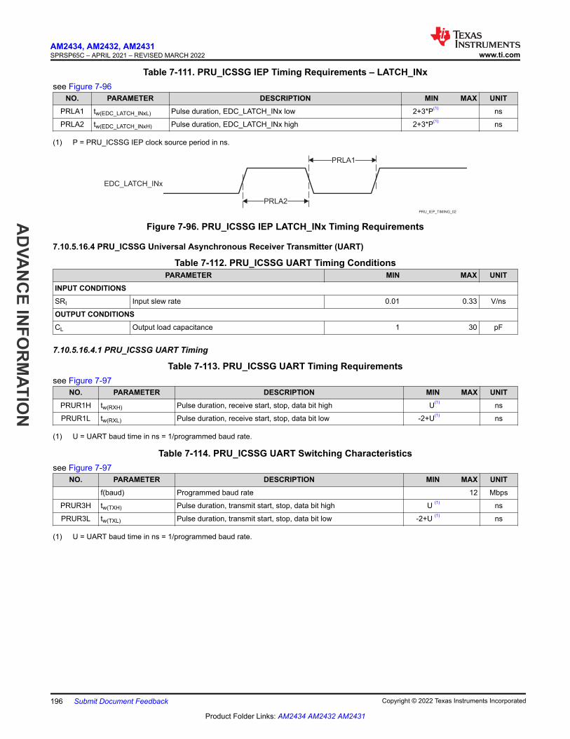
Table 7-111. PRU_ICSSG IEP Timing Requirements – LATCH_INxsee Figure 7-96
NO. PARAMETER DESCRIPTION MIN MAX UNITPRLA1 tw(EDC_LATCH_INxL) Pulse duration, EDC_LATCH_INx low 2+3*P(1) ns
PRLA2 tw(EDC_LATCH_INxH) Pulse duration, EDC_LATCH_INx high 2+3*P(1) ns
(1) P = PRU_ICSSG IEP clock source period in ns.
EDC_LATCH_INx
PRLA2
PRU_IEP_TIMING_02
PRLA1
Figure 7-96. PRU_ICSSG IEP LATCH_INx Timing Requirements
7.10.5.16.4 PRU_ICSSG Universal Asynchronous Receiver Transmitter (UART)
Table 7-112. PRU_ICSSG UART Timing ConditionsPARAMETER MIN MAX UNIT
INPUT CONDITIONSSRI Input slew rate 0.01 0.33 V/ns
OUTPUT CONDITIONSCL Output load capacitance 1 30 pF
7.10.5.16.4.1 PRU_ICSSG UART Timing
Table 7-113. PRU_ICSSG UART Timing Requirementssee Figure 7-97
NO. PARAMETER DESCRIPTION MIN MAX UNITPRUR1H tw(RXH) Pulse duration, receive start, stop, data bit high U(1) ns
PRUR1L tw(RXL) Pulse duration, receive start, stop, data bit low -2+U(1) ns
(1) U = UART baud time in ns = 1/programmed baud rate.
Table 7-114. PRU_ICSSG UART Switching Characteristicssee Figure 7-97
NO. PARAMETER DESCRIPTION MIN MAX UNITf(baud) Programmed baud rate 12 Mbps
PRUR3H tw(TXH) Pulse duration, transmit start, stop, data bit high U (1) ns
PRUR3L tw(TXL) Pulse duration, transmit start, stop, data bit low -2+U (1) ns
(1) U = UART baud time in ns = 1/programmed baud rate.
AM2434, AM2432, AM2431SPRSP65C – APRIL 2021 – REVISED MARCH 2022 www.ti.com
AD
VAN
CE IN
FOR
MATIO
N
196 Submit Document Feedback Copyright © 2022 Texas Instruments Incorporated
Product Folder Links: AM2434 AM2432 AM2431

PRUR3L
Start
Bit
Data Bits
PRG _UART0_TXDi
PRU_UART_TIMING_01
PRUR3H
PRUR1L
Data Bits
Bit
Start
PRG _UART0_RXDi
PRUR1H
(1)
(1)
(1) i in PRG _UART0_RXD and PRG _UART0_TXD = 0, 1 or 2i i
Figure 7-97. PRU_ICSSG UART Timing Requirements and Switching Characteristics
7.10.5.16.5 PRU_ICSSG Enhanced Capture Peripheral (ECAP)
Table 7-115. PRU_ICSSG ECAP Timing ConditionsPARAMETER MIN MAX UNIT
INPUT CONDITIONSSRI Input slew rate 1 3 V/ns
OUTPUT CONDITIONSCL Output load capacitance 2 7 pF
7.10.5.16.5.1 PRU_ICSSG ECAP Timing
Table 7-116. PRU_ICSSG ECAP Timing Requirementssee Figure 7-98
NO. PARAMETER DESCRIPTION MIN MAX UNITPREP1 tw(CAP) Pulse Duration, CAP (asynchronous) 2+2*P(1) ns
PREP2 tw(SYNCI) Pulse Duration, SYNCI (asynchronous) 2+2*P(1) ns
(1) P = CORE_CLK period in ns.
CAP
PREP1
SYNCI
PREP2
Figure 7-98. PRU_ICSSG ECAP Timing
Table 7-117. PRU_ICSSG ECAP Switching Characteristicssee Figure 7-99
NO. PARAMETER DESCRIPTION MIN MAX UNITPREP3 tw(APWM) Pulse Duration, APWM high/low 2*P(1) ns
PREP4 tw(SYNCO) Pulse Duration, SYNCO (asynchronous) P(1) ns
(1) P = CORE_CLK period in ns.
www.ti.comAM2434, AM2432, AM2431
SPRSP65C – APRIL 2021 – REVISED MARCH 2022
AD
VAN
CE
INFO
RM
ATIO
N
Copyright © 2022 Texas Instruments Incorporated Submit Document Feedback 197
Product Folder Links: AM2434 AM2432 AM2431

APWM
PREP3
SYNCO
PREP4
Figure 7-99. PRU_ICSSG ECAP Switching Characteristics
7.10.5.16.6 PRU_ICSSG RGMII, MII_RT, and Switch
For more information, see Programmable Real-Time Unit Subsystem and Industrial Communication Subsystem - Gigabit (PRU_ICSSG) section in Processors and Accelerators chapter in the device TRM.
7.10.5.16.6.1 PRU_ICSSG MDIO Timing
Table 7-118, Table 7-119, Table 7-120, and Figure 7-100 present timing conditions, requirements, and switching characteristics for PRU_ICSSG MDIO.
Table 7-118. PRU_ICSSG MDIO Timing ConditionsPARAMETER MIN MAX UNIT
INPUT CONDITIONSSRI Input slew rate 0.9 3.6 V/ns
OUTPUT CONDITIONSCL Output load capacitance 10 470 pF
Table 7-119. PRU_ICSSG MDIO Timing Requirementssee Figure 7-100
NO. PARAMETER MIN MAX UNITMDIO1 tsu(MDIO_MDC) Setup time, MDIO[x]_MDIO valid before MDIO[x]_MDC high 90 ns
MDIO2 th(MDC_MDIO) Hold time, MDIO[x]_MDIO valid after MDIO[x]_MDC high 0 ns
Table 7-120. PRU_ICSSG MDIO Switching Characteristicssee Figure 7-100
NO. PARAMETER MIN MAX UNITMDIO3 tc(MDC) Cycle time, MDIO[x]_MDC 400 ns
MDIO4 tw(MDCH) Pulse Duration, MDIO[x]_MDC high 160 ns
MDIO5 tw(MDCL) Pulse Duration, MDIO[x]_MDC low 160 ns
MDIO7 td(MDC_MDIO) Delay time, MDIO[x]_MDC low to MDIO[x]_MDIO valid -150 150 ns
AM2434, AM2432, AM2431SPRSP65C – APRIL 2021 – REVISED MARCH 2022 www.ti.com
AD
VAN
CE IN
FOR
MATIO
N
198 Submit Document Feedback Copyright © 2022 Texas Instruments Incorporated
Product Folder Links: AM2434 AM2432 AM2431

MDIO3
MDIO1
MDIO2
MDIO7
MDIO4
MDIO5
MDIO[x]_MDC
MDIO[x]_MDIO(input)
MDIO[x]_MDIO(output)
CPSW2G_MDIO_TIMING_01
Figure 7-100. PRU_ICSSG MDIO Timing Requirements and Switching Characteristics
7.10.5.16.6.2 PRU_ICSSG MII Timing
Note
In order to ensure the MII_G_RT I/O timing values published in the device data sheet, the PRU_ICSSG ICSSGn_CORE_CLK (where n = 0 to 1) core clock must be configured for 200 MHz, 225 MHz, or 250 MHz and the TX_CLK_DELAYn (where n = 0 or 1) bit field in the ICSSG_TXCFG0/1 register must be set to 0h (default value).
Table 7-121, Table 7-122, Figure 7-101, Table 7-123, Figure 7-102, Table 7-124, Figure 7-103, Table 7-125, and Figure 7-104 present timing conditions, requirements, and switching characteristics for PRU_ICSSG MII.
Table 7-121. PRU_ICSSG MII Timing ConditionsPARAMETER MIN MAX UNIT
INPUT CONDITIONSSRI Input slew rate 0.9 3.6 V/ns
OUTPUT CONDITIONSCL Output load capacitance 2 20 pF
Table 7-122. PRU_ICSSG MII Timing Requirements – MII[x]_RX_CLKsee Figure 7-101
NO. PARAMETER DESCRIPTION MODE MIN MAX UNIT
PMIR1 tc(RX_CLK) Cycle time, MII[x]_RX_CLK10 Mbps 399.96 400.04 ns
100 Mbps 39.996 40.004 ns
PMIR2 tw(RX_CLKH) Pulse Duration, MII[x]_RX_CLK High10 Mbps 140 260 ns
100 Mbps 14 26 ns
PMIR3 tw(RX_CLKL) Pulse Duration, MII[x]_RX_CLK Low10 Mbps 140 260 ns
100 Mbps 14 26 ns
www.ti.comAM2434, AM2432, AM2431
SPRSP65C – APRIL 2021 – REVISED MARCH 2022
AD
VAN
CE
INFO
RM
ATIO
N
Copyright © 2022 Texas Instruments Incorporated Submit Document Feedback 199
Product Folder Links: AM2434 AM2432 AM2431
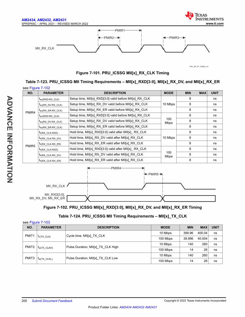
MII_RX_CLK
PMIR2 PMIR3
PMIR1
PRU_MII_RT_TIMING_04
Figure 7-101. PRU_ICSSG MII[x]_RX_CLK Timing
Table 7-123. PRU_ICSSG MII Timing Requirements – MII[x]_RXD[3:0], MII[x]_RX_DV, and MII[x]_RX_ERsee Figure 7-102
NO. PARAMETER DESCRIPTION MODE MIN MAX UNIT
PMIR4
tsu(RXD-RX_CLK) Setup time, MII[x]_RXD[3:0] valid before MII[x]_RX_CLK
10 Mbps
8 ns
tsu(RX_DV-RX_CLK) Setup time, MII[x]_RX_DV valid before MII[x]_RX_CLK 8 ns
tsu(RX_ER-RX_CLK) Setup time, MII[x]_RX_ER valid before MII[x]_RX_CLK 8 ns
tsu(RXD-RX_CLK) Setup time, MII[x]_RXD[3:0] valid before MII[x]_RX_CLK100
Mbps
8 ns
tsu(RX_DV-RX_CLK) Setup time, MII[x]_RX_DV valid before MII[x]_RX_CLK 8 ns
tsu(RX_ER-RX_CLK) Setup time, MII[x]_RX_ER valid before MII[x]_RX_CLK 8 ns
PMIR5
th(RX_CLK-RXD) Hold time, MII[x]_RXD[3:0] valid after MII[x]_ RX_CLK
10 Mbps
8 ns
th(RX_CLK-RX_DV) Hold time, MII[x]_RX_DV valid after MII[x]_RX_CLK 8 ns
th(RX_CLK-RX_ER) Hold time, MII[x]_RX_ER valid after MII[x]_RX_CLK 8 ns
th(RX_CLK-RXD) Hold time, MII[x]_RXD[3:0] valid after MII[x]_ RX_CLK100
Mbps
8 ns
th(RX_CLK-RX_DV) Hold time, MII[x]_RX_DV valid after MII[x]_RX_CLK 8 ns
th(RX_CLK-RX_ER) Hold time, MII[x]_RX_ER valid after MII[x]_RX_CLK 8 ns
MII_RX_CLK
PMIR4
PMIR5
MII_RXD[3:0],MII_RX_DV, MII_RX_ER
Figure 7-102. PRU_ICSSG MII[x]_RXD[3:0], MII[x]_RX_DV, and MII[x]_RX_ER Timing
Table 7-124. PRU_ICSSG MII Timing Requirements – MII[x]_TX_CLKsee Figure 7-103
NO. PARAMETER DESCRIPTION MODE MIN MAX UNIT
PMIT1 tc(TX_CLK) Cycle time, MII[x]_TX_CLK10 Mbps 399.96 400.04 ns
100 Mbps 39.996 40.004 ns
PMIT2 tw(TX_CLKH) Pulse Duration, MII[x]_TX_CLK High10 Mbps 140 260 ns
100 Mbps 14 26 ns
PMIT3 tw(TX_CLKL) Pulse Duration, MII[x]_TX_CLK Low10 Mbps 140 260 ns
100 Mbps 14 26 ns
AM2434, AM2432, AM2431SPRSP65C – APRIL 2021 – REVISED MARCH 2022 www.ti.com
AD
VAN
CE IN
FOR
MATIO
N
200 Submit Document Feedback Copyright © 2022 Texas Instruments Incorporated
Product Folder Links: AM2434 AM2432 AM2431

MII_TX_CLK
PMIT2 PMIT3
PMIT1
Figure 7-103. PRU_ICSSG MII[x]_TX_CLK Timing
Table 7-125. PRU_ICSSG MII Switching Characteristics – MII[x]_TXD[3:0] and MII[x]_TX_ENsee Figure 7-104
NO. PARAMETER DESCRIPTION MODE MIN MAX UNIT
PMIT4
td(TX_CLK-TXD) Delay time, MII[x]_TX_CLK High to MII[x]_TXD[3:0] valid10 Mbps
0 25 ns
td(TX_CLK-TX_EN) Delay time, MII[x]_TX_CLK to MII[x]_TX_EN valid 0 25 ns
td(TX_CLK-TXD) Delay time, MII[x]_TX_CLK High to MII[x]_TXD[3:0] valid 100 Mbps
0 25 ns
td(TX_CLK-TX_EN) Delay time, MII[x]_TX_CLK to MII[x]_TX_EN valid 0 25 ns
PMIT4
MII_TX_CLK
MII_TXD[3:0], MII_TX_EN
Figure 7-104. PRU_ICSSG MII[x]_TXD[3:0], MII[x]_TX_EN Timing
7.10.5.16.6.3 PRU_ICSSG RGMII Timing
Table 7-126, Table 7-127, Table 7-128, Figure 7-105, Table 7-129, Table 7-130, and Figure 7-106 present timing conditions, requirements, and switching characteristics for PRU_ICSSG RGMII.
Table 7-126. PRU_ICSSG RGMII Timing ConditionsPARAMETER MIN MAX UNIT
INPUT CONDITIONSSRI Input slew rate 2.65 5 V/ns
OUTPUT CONDITIONSCL Output load capacitance 2 20 pF
Table 7-127. PRU_ICSSG RGMII Timing Requirements – RGMII[x]_RXCsee Figure 7-105
NO. PARAMETER DESCRIPTION MODE MIN MAX UNITRGMII1 tc(RXC) Cycle time, RGMII[x]_RXC 10 Mbps 360 440 ns
100 Mbps 36 44 ns
1000 Mbps 7.2 8.8 ns
RGMII2 tw(RXCH) Pulse duration, RGMII[x]_RXC high 10 Mbps 160 240 ns
100 Mbps 16 24 ns
1000 Mbps 3.6 4.4 ns
RGMII3 tw(RXCL) Pulse duration, RGMII[x]_RXC low 10 Mbps 160 240 ns
100 Mbps 16 24 ns
1000 Mbps 3.6 4.4 ns
www.ti.comAM2434, AM2432, AM2431
SPRSP65C – APRIL 2021 – REVISED MARCH 2022
AD
VAN
CE
INFO
RM
ATIO
N
Copyright © 2022 Texas Instruments Incorporated Submit Document Feedback 201
Product Folder Links: AM2434 AM2432 AM2431

Table 7-128. PRU_ICSSG RGMII Timing Requirements – RGMII[x]_RD[3:0] and RGMII[x]_RX_CTLsee Figure 7-105
NO. PARAMETER DESCRIPTION MODE MIN MAX UNITRGMII4 tsu(RD-RXC) Setup time, RGMII[x]_RD[3:0] valid before RXC high/low 10 Mbps 1 ns
100 Mbps 1 ns
1000 Mbps 1 ns
tsu(RX_CTL-RXC) Setup time, RGMII[x]_RX_CTL valid before RGMII[x]_RXC high/low
10 Mbps 1 ns
100 Mbps 1 ns
1000 Mbps 1 ns
RGMII5 th(RXC-RD) Hold time, RGMII[x]_RD[3:0] valid after RGMII[x]_RXC high/low
10 Mbps 1 ns
100 Mbps 1 ns
1000 Mbps 1 ns
th(RXC-RX_CTL) Hold time, RGMII[x]_RX_CTL valid after RGMII[x]_RXC high/low
10 Mbps 1 ns
100 Mbps 1 ns
1000 Mbps 1 ns
RGMII[x] RD 3_ [ :0](B)
RGMII[x] RX_CTL_(B)
RGMII[x] RXC_(A)
RGMII4
RXERRRXDV
2nd Half-byte1st Half-byte
RGMII2RGMII3
RGMII1
RGMII5
A. RGMII[x]_RXC must be externally delayed relative to the data and control pins.B. Data and control information is received using both edges of the clocks. RGMII[x]_RD[3:0] carries data bits 3-0 on the rising edge of
RGMII[x]_RXC and data bits 7-4 on the falling edge of RGMII[x]_RXC. Similarly, RGMII[x]_RX_CTL carries RXDV on rising edge of RGMII[x]_RXC and RXERR on falling edge of RGMII[x]_RXC.
Figure 7-105. PRU_ICSSG RGMII[x]_RXC, RGMII[x]_RD[3:0], RGMII[x]_RX_CTL Timing Requirements - RGMII Mode
Table 7-129. PRU_ICSSG RGMII Switching Characteristics – RGMII[x]_TXCsee Figure 7-106
NO. PARAMETER DESCRIPTION MODE MIN MAX UNITRGMII6 tc(TXC) Cycle time, RGMII[x]_TXC 10 Mbps 360 440 ns
100 Mbps 36 44 ns
1000 Mbps 7.2 8.8 ns
RGMII7 tw(TXCH) Pulse duration, RGMII[x]_TXC high 10 Mbps 160 240 ns
100 Mbps 16 24 ns
1000 Mbps 3.6 4.4 ns
RGMII8 tw(TXCL) Pulse duration, RGMII[x]_TXC low 10 Mbps 160 240 ns
100 Mbps 16 24 ns
1000 Mbps 3.6 4.4 ns
AM2434, AM2432, AM2431SPRSP65C – APRIL 2021 – REVISED MARCH 2022 www.ti.com
AD
VAN
CE IN
FOR
MATIO
N
202 Submit Document Feedback Copyright © 2022 Texas Instruments Incorporated
Product Folder Links: AM2434 AM2432 AM2431

Table 7-130. PRU_ICSSG RGMII Switching Characteristics – RGMII[x]_TD[3:0] and RGMII[x]_TX_CTLsee Figure 7-106
NO. PARAMETER DESCRIPTION MODE MIN MAX UNITRGMII9 tosu(TD-TXC) Output setup time, RGMII[x]_TD[3:0] valid to RGMII[x]_TXC
high/low10 Mbps 1.2 ns
100 Mbps 1.2 ns
1000 Mbps 1.2 ns
tosu(TX_CTL-TXC) Output setup time, RGMII[x]_TX_CTL valid to RGMII[x]_TXC high/low
10 Mbps 1.2 ns
100 Mbps 1.2 ns
1000 Mbps 1.2 ns
RGMII10 toh(TXC-TD) Output setup time, RGMII[x]_TD[3:0] valid after RGMII[x]_TXC high/low
10 Mbps 1.2 ns
100 Mbps 1.2 ns
1000 Mbps 1.2 ns
toh(TXC-TX_CTL) Output setup time, RGMII[x]_TX_CTL valid after RGMII[x]_TXC high/low
10 Mbps 1.2 ns
100 Mbps 1.2 ns
1000 Mbps 1.2 ns
RGMII[x]_TXC(A)
RGMII[x]_TD[3:0](B)
RGMII[x] TX_CTL_(B)
RGMII9
1st Half-byte
TXERRTXEN
2nd Half-byte
RGMII7RGMII8
RGMII6
RGMII10
A. TXC is delayed internally before being driven to the RGMII[x]_TXC pin. This internal delay is always enabled.B. Data and control information is received using both edges of the clocks. RGMII[x]_TD[3:0] carries data bits 3-0 on the rising edge of
RGMII[x]_TXC and data bits 7-4 on the falling edge of RGMII[x]_TXC. Similarly, RGMII[x]_TX_CTL carries TXEN on rising edge of RGMII[x]_TXC and TXERR on falling edge of RGMII[x]_TXC.
Figure 7-106. PRU_ICSSG RGMII[x]_TXC, RGMII[x]_TD[3:0], and RGMII[x]_TX_CTL Switching Characteristics - RGMII Mode
7.10.5.17 Timers
For more details about features and additional description information on the device Timers, see the corresponding subsections within Signal Descriptions and Detailed Description sections.
Table 7-131. Timer Timing ConditionsPARAMETER MIN MAX UNIT
INPUT CONDITIONSSRI Input slew rate 0.5 5 V/ns
OUTPUT CONDITIONSCL Output load capacitance 2 10 pF
Table 7-132. Timer Input Timing Requirementssee Figure 7-107
NO. PARAMETER DESCRIPTION MODE MIN MAX UNITT1 tw(TINPH) Pulse duration, high CAPTURE 2 + 4P(1) ns
www.ti.comAM2434, AM2432, AM2431
SPRSP65C – APRIL 2021 – REVISED MARCH 2022
AD
VAN
CE
INFO
RM
ATIO
N
Copyright © 2022 Texas Instruments Incorporated Submit Document Feedback 203
Product Folder Links: AM2434 AM2432 AM2431

Table 7-132. Timer Input Timing Requirements (continued)see Figure 7-107
NO. PARAMETER DESCRIPTION MODE MIN MAX UNITT2 tw(TINPL) Pulse duration, low CAPTURE 2 + 4P(1) ns
(1) P = functional clock period in ns.
Table 7-133. Timer Output Switching Characteristicssee Figure 7-107
NO. PARAMETER DESCRIPTION MODE MIN MAX UNITT3 tw(TOUTH) Pulse duration, high PWM -2 + 4P(1) ns
T4 tw(TOUTL) Pulse duration, low PWM -2 + 4P(1) ns
(1) P = functional clock period in ns.
T1 T2
TIMER_IOx (inputs)
TIMER_01
T3 T4
TIMER_IOx (outputs)
Figure 7-107. Timer Timing Requirements and Switching Characteristics
For more information, see Timers section in Peripherals chapter in the device TRM.
7.10.5.18 UART
For more details about features and additional description information on the device Universal Asynchronous Receiver Transmitter, see the corresponding subsections within Signal Descriptions and Detailed Description sections.
Table 7-134. UART Timing ConditionsPARAMETER MIN MAX UNIT
INPUT CONDITIONSSRI Input slew rate 0.5 5 V/ns
OUTPUT CONDITIONSCL Output load capacitance 1 30 pF
Table 7-135. UART Timing Requirements see Figure 7-108
NO. PARAMETER DESCRIPTION MIN MAX UNIT4 tw(RX) Pulse width, receive data bit, high or low 0.95U(1) 1.05U(1) ns
5 tw(CTS) Pulse width, receive start bit, high or low 0.95U(1) ns
(1) U = UART baud time in ns = 1/programmed baud rate.
Table 7-136. UART Switching Characteristicssee Figure 7-108
NO. PARAMETER DESCRIPTION MODE MIN MAX UNIT
f(baud) Programmable baud rate15 pF TDB Mbps
30 pF 0.115 Mbps
1 td(CTS-TX) Delay time, CTS bit to transmit data 30 ns
2 tw(TX) Pulse width, transmit data bit, high or low U - 2.2(1) U + 2.2(1) ns
AM2434, AM2432, AM2431SPRSP65C – APRIL 2021 – REVISED MARCH 2022 www.ti.com
AD
VAN
CE IN
FOR
MATIO
N
204 Submit Document Feedback Copyright © 2022 Texas Instruments Incorporated
Product Folder Links: AM2434 AM2432 AM2431

Table 7-136. UART Switching Characteristics (continued)see Figure 7-108
NO. PARAMETER DESCRIPTION MODE MIN MAX UNIT3 tw(RTS) Pulse width, transmit start bit, high or low U - 2.2(1) ns
(1) U = UART baud time in ns = 1/programmed baud rate.
Figure 7-108. UART Timing Requirements and Switching Characteristics
For more information, see Universal Asynchronous Receiver/Transmitter (UART) section in Peripherals chapter in the device TRM.
7.10.5.19 USB
The USB 2.0 subsystem is compliant with the Universal Serial Bus (USB) Specification, revision 2.0. Refer to the specification for timing details.
The USB 3.1 GEN1 subsystem is compliant with the Universal Serial Bus (USB) 3.1 Specification, revision 1.0. Refer to the specification for timing details.
For more details about features and additional description information on the device Universal Serial Bus Subsystem (USB), see the corresponding subsections within Signal Descriptions and Detailed Description sections.
7.10.6 Emulation and Debug
For more details about features and additional description information on the device Trace and JTAG interfaces, see the corresponding subsections within Signal Descriptions and Detailed Description sections.
7.10.6.1 Trace
Table 7-137. Trace Timing ConditionsPARAMETER MIN MAX UNIT
OUTPUT CONDITIONSCL Output load capacitance 2 5 pF
PCB CONNECTIVITY REQUIREMENTS
td(Trace Mismatch) Propagation delay mismatch across all tracesVDDSHV3 = 1.8V 200 ps
VDDSHV3 =3.3V 100 ps
www.ti.comAM2434, AM2432, AM2431
SPRSP65C – APRIL 2021 – REVISED MARCH 2022
AD
VAN
CE
INFO
RM
ATIO
N
Copyright © 2022 Texas Instruments Incorporated Submit Document Feedback 205
Product Folder Links: AM2434 AM2432 AM2431

Table 7-138. Trace Switching CharacteristicsNO. PARAMETER MIN MAX UNIT
1.8V ModeDBTR1 tc(TRC_CLK) Cycle time, TRC_CLK 6.50 ns
DBTR2 tw(TRC_CLKH) Pulse width, TRC_CLK high 2.50 ns
DBTR3 tw(TRC_CLKL) Pulse width, TRC_CLK low 2.50 ns
DBTR4 tosu(TRC_DATAV-TRC_CLK)
Output setup time, TRC_DATA valid to TRC_CLK edge 0.81 ns
DBTR5 toh(TRC_CLK-TRC_DATAI) Output hold time, TRC_CLK edge to TRC_DATA invalid 0.81 ns
DBTR6 tosu(TRC_CTLV-TRC_CLK) Output setup time, TRC_CTL valid to TRC_CLK edge 0.81 ns
DBTR7 toh(TRC_CLK-TRC_CTLI) Output hold time, TRC_CLK edge to TRC_CTL invalid 0.81 ns
3.3V ModeDBTR1 tc(TRC_CLK) Cycle time, TRC_CLK 8.67 ns
DBTR2 tw(TRC_CLKH) Pulse width, TRC_CLK high 3.58 ns
DBTR3 tw(TRC_CLKL) Pulse width, TRC_CLK low 3.58 ns
DBTR4 tosu(TRC_DATAV-TRC_CLK)
Output setup time, TRC_DATA valid to TRC_CLK edge 1.08 ns
DBTR5 toh(TRC_CLK-TRC_DATAI) Output hold time, TRC_CLK edge to TRC_DATA invalid 1.08 ns
DBTR6 tosu(TRC_CTLV-TRC_CLK) Output setup time, TRC_CTL valid to TRC_CLK edge 1.08 ns
DBTR7 toh(TRC_CLK-TRC_CTLI) Output hold time, TRC_CLK edge to TRC_CTL invalid 1.08 ns
TRC_DATATRC_CTL
TRC_CLK( )
( )(Ideal)Worst Case 1
Worst Case 2
DBTR1
DBTR2 DBTR3
DBTR4
DBTR6
DBTR5
DBTR7
DBTR4
DBTR6
DBTR5
DBTR7
SPRSP08_Debug_01
Figure 7-109. Trace Switching Characteristics
7.10.6.2 JTAG
Table 7-139. JTAG Timing ConditionsPARAMETER MIN MAX UNIT
INPUT CONDITIONSSRI Input slew rate 0.5 2.0 V/ns
OUTPUT CONDITIONSCL Output load capacitance 5 15 pF
Table 7-140. JTAG Timing Requirementssee Figure 7-110
NO. MIN MAX UNITJ1 tc(TCK) Cycle time minimum, TCK 45.5 ns
J2 tw(TCKH) Pulse width minimum, TCK high 18.2 ns
J3 tw(TCKL) Pulse width minimum, TCK low 18.2 ns
J4tsu(TDI-TCK) Input setup time minimum, TDI valid to TCK high 4 ns
tsu(TMS-TCK) Input setup time minimum, TMS valid to TCK high 4 ns
AM2434, AM2432, AM2431SPRSP65C – APRIL 2021 – REVISED MARCH 2022 www.ti.com
AD
VAN
CE IN
FOR
MATIO
N
206 Submit Document Feedback Copyright © 2022 Texas Instruments Incorporated
Product Folder Links: AM2434 AM2432 AM2431

Table 7-140. JTAG Timing Requirements (continued)see Figure 7-110
NO. MIN MAX UNIT
J5th(TCK-TDI) Input hold time minimum, TDI valid from TCK high 2 ns
th(TCK-TMS) Input hold time minimum, TMS valid from TCK high 2 ns
Table 7-141. JTAG Switching Characteristicssee Figure 7-110
NO. PARAMETER MIN MAX UNITJ6 td(TCKL-TDOI) Delay time minimum, TCK low to TDO invalid 0 ns
J7 td(TCKL-TDOV) Delay time maximum, TCK low to TDO valid 14 ns
TDO
J2
J1
J4
TCK
J5
TDI / TMS
J3
J6J7
J4 J5
Figure 7-110. JTAG Timing Requirements and Switching Characteristics
www.ti.comAM2434, AM2432, AM2431
SPRSP65C – APRIL 2021 – REVISED MARCH 2022
AD
VAN
CE
INFO
RM
ATIO
N
Copyright © 2022 Texas Instruments Incorporated Submit Document Feedback 207
Product Folder Links: AM2434 AM2432 AM2431

8 Detailed Description8.1 OverviewAM243x is an extension of the Sitara’s industrial-grade family of heterogeneous Arm processors. AM243x is built for industrial applications, such as motor drives and programmable logic controllers (PLCs), which require a unique combination of real-time processing and communications with applications processing. AM243x combines two instances of Sitara’s gigabit TSN-enabled PRU-ICSSG, up to four Cortex-R5F MCUs and a Cortex-M4F MCU.
AM243x is architected to provide real-time performance through the high-performance R5Fs, Tightly-Coupled Memory banks, configurable SRAM partitioning, and low-latency paths to and from peripherals for rapid data movement in and out of the SoC. This deterministic architecture allows for AM243x to handle the tight control loops found in servo drives, while the peripherals like FSI, GPMC, PWMs, sigma delta decimation filters, and absolute encoder interfaces help enable a number of different architectures found in these systems.
The PRU-ICSSG in AM243x provides the flexible industrial communications capability necessary to run gigabit TSN, EtherCAT, PROFINET, EtherNet/IP, and various other protocols. In addition, the PRU-ICSSG also enables additional interfaces in the SoC including sigma delta decimation filters and absolute encoder interfaces.
Functional safety features can be enabled through the integrated Cortex-M4F along with its dedicated peripherals which can all be isolated from the rest of the SoC. AM243x also supports secure boot.
Note
For more information on features, subsystems, and architecture of superset device System on Chip (SoC), see the device TRM.
AM2434, AM2432, AM2431SPRSP65C – APRIL 2021 – REVISED MARCH 2022 www.ti.com
AD
VAN
CE IN
FOR
MATIO
N
208 Submit Document Feedback Copyright © 2022 Texas Instruments Incorporated
Product Folder Links: AM2434 AM2432 AM2431

8.2 Processor Subsystems8.2.1 Arm Cortex-R5F Subsystem (R5FSS)
The R5FSS is a dual-core implementation of the Arm® Cortex®-R5F processor configured for dual/single-core operation. It also includes accompanying memories (L1 caches and tightly-coupled memories), standard Arm® CoreSight™ debug and trace architecture, integrated Vectored Interrupt Manager (VIM), ECC Aggregators, and various wrappers for protocol conversion and address translation for easy integration into the SoC.
Note
The Cortex®-R5F processor is a Cortex-R5 processor that includes the optional Floating Point Unit (FPU) extension.
For more information, see Dual-R5F Subsystem (R5FSS) section in Processors and Accelerators chapter in the device TRM.
8.2.2 Arm Cortex-M4F (M4FSS)
The M4FSS module on the AM243x device provides a safety channel (secondary channel - working in conjunction with an external microcontroller)- or- a general purpose MCU.
The M4FSS module supports the following features:• Cortex M4F With MPU• ARMv7-M architecture• Support for Nested Vectored Interrupt Controller (NVIC) with 64 inputs• Ability to executed code from internal or external memories• 192 KB of SRAM (I-Code)• 64 KB of SRAM (D-Code)• External access to internal memories if allowed• Debug Support Including:
– DAP based Debug to the CPU Core– Full Debug Features of CPU Core are enabled– Standard ITM trace– CTM Cross Trigger– ETM Trace Support
• Fault Detection and Correction– SECDED ECC protection on I-CODE– SECDED ECC protection on D-CODE– Fault Error Interrupt Output
For more information, see Arm Cortex M4F Subsystem (M4FSS) section in Processors and Accelerators chapter in the device TRM.
www.ti.comAM2434, AM2432, AM2431
SPRSP65C – APRIL 2021 – REVISED MARCH 2022
AD
VAN
CE
INFO
RM
ATIO
N
Copyright © 2022 Texas Instruments Incorporated Submit Document Feedback 209
Product Folder Links: AM2434 AM2432 AM2431

8.3 Accelerators and Coprocessors8.3.1 Programmable Real-Time Unit Subsystem and Industrial Communication Subsystem (PRU_ICSSG)
The PRU_ICSSG module supports the following main features:• 3x PRUs
– General-Purpose PRU (PRU)– Real-Time PRU(RTU_PRU)– Transmit PRU (TX_PRU)
• 2x Ethernet MII_G_RT configurable connection to PRUs– Up to 2x RGMII ports– Up to 2x MII ports– RX Classifier
• 2x Industrial Ethernet Peripheral (IEP) to manage and generate industrial Ethernet functions• 2x Industrial Ethernet 64-bit timers, each with 10 capture and 16 compare events, along with slow and fast
compensation.• 1x MDIO• 1x UART, with a dedicated 192-MHz clock input• Supports up to 4 sets of 3-phased motor control, with 12 primary and 12 complimentary programmable PWM
outputs.• Supports up to 9 safety events with optional external trip I/O per PWM set with hardware glitch filter.• 1x Enhanced Capture Module (ECAP)• 1x Interrupt Controller (INTC)
– 160 input events supported – 96 external, 64 internal• Flexible power management support• Integrated switched central resource with programmable priority• All memories support ECC
For more information, see Programmable Real-Time Unit Subsystem and Industrial Communication Subsystem - Gigabit (PRU_ICSSG) section in Processors and Accelerators chapter in the device TRM.
8.4 Other Subsystems8.4.1 PDMA Controller
The Peripheral DMA is a simple DMA which has been architected to specifically meet the data transfer needs of peripherals, which perform data transfers using memory mapped registers accessed via a standard non-coherent bus fabric. The PDMA module is intended to be located close to one or more peripherals which require an external DMA for data movement and is architected to reduce cost by using VBUSP interfaces and supporting only statically configured Transfer Request (TR) operations.
The PDMA is only responsible for performing the data movement transactions which interact with the peripherals themselves. Data which is read from a given peripheral is packed by a PDMA source channel into a PSI-L data stream which is then sent to a remote peer UDMA-P destination channel which then performs the movement of the data into memory. Likewise, a remote UDMA-P source channel fetches data from memory and transfers it to a peer PDMA destination channel over PSI-L which then performs the writes to the peripheral.
The PDMA architecture is intentionally heterogeneous (UDMA-P + PDMA) to right size the data transfer complexity at each point in the system to match the requirements of whatever is being transferred to or from. Peripherals are typically FIFO based and do not require multi-dimensional transfers beyond their FIFO dimensioning requirements, so the PDMA transfer engines are kept simple with only a few dimensions (typically for sample size and FIFO depth), hardcoded address maps, and simple triggering capabilities.
Multiple source and destination channels are provided within the PDMA which allow multiple simultaneous transfer operations to be ongoing. The DMA controller maintains state information for each of the channels and employs round-robin scheduling between channels in order to share the underlying DMA hardware.
There are five PDMA modules in the device.
For more information, see PDMA Controller section in DMA Controllers chapter in the device TRM.
AM2434, AM2432, AM2431SPRSP65C – APRIL 2021 – REVISED MARCH 2022 www.ti.com
AD
VAN
CE IN
FOR
MATIO
N
210 Submit Document Feedback Copyright © 2022 Texas Instruments Incorporated
Product Folder Links: AM2434 AM2432 AM2431

8.4.2 Peripherals8.4.2.1 ADC
The analog-to-digital converter (ADC) module is an single-channel general purpose analog-to-digital converter with a 8-input analog multiplexer, which supports 12-bit conversion samples from an analog front end (AFE).
There is one ADC module in the device.
Note
The AM243x_ALX package only supports 10-bit conversions.
For more information, see Analog-to-Digital Converter (ADC) section in Peripherals chapter in the device TRM.
8.4.2.2 DCC
The Dual Clock Comparator (DCC) is used to determine the accuracy of a clock signal during the time execution of an application. Specifically, the DCC is designed to detect drifts from the expected clock frequency. The desired accuracy can be programed based on calculation for each application. The DCC measures the frequency of a selectable clock source using another input clock as a reference.
The device has seven instances of DCC modules.
For more information, see Dual Clock Comparator (DCC) section in Peripherals chapter in the device TRM.
8.4.2.3 Dual Date Rate (DDR) External Memory Interface (DDRSS)
Integrated in MAIN domain: one instance of DDR Subsystem (DDRSS) is used as an interface to external RAM devices which can be utilized for storing program or data. DDRSS provides the following main features:
• Support of DDR4 / LPDDR4 memory types• 16-bit memory bus interface with in-line ECC• System bus interface: little endian only with 128-bit data width• Configuration bus Interface: little endian only with 32-bit data width• Support of dual rank configuration• Support of automatic idle power saving mode when no or low activity is detected• Class of Service (CoS) - three latency classes supported• Prioritized refresh scheduling• Statistical counters for performance management
For more information, see DDR Subsystem (DDRSS) section in Peripherals chapter in the device TRM.
8.4.2.4 ECAP
This section describes the Enhanced Capture (ECAP) module for the device.
For more information, see Enhanced Capture (ECAP) Module section in Peripherals chapter in the device TRM.
8.4.2.5 EPWM
An effective PWM peripheral must be able to generate complex pulse width waveforms with minimal CPU overhead or intervention. It needs to be highly programmable and very flexible while being easy to understand and use. The EPWM unit described here addresses these requirements by allocating all needed timing and control resources on a per PWM channel basis. Cross coupling or sharing of resources has been avoided; instead, the EPWM is built up from smaller single channel modules with separate resources and that can operate together as required to form a system. This modular approach results in an orthogonal architecture and provides a more transparent view of the peripheral structure, helping users to understand its operation quickly.
In the further description the letter x within a signal or module name is used to indicate a generic EPWM instance on a device. For example, output signals EPWMxA and EPWMxB refer to the output signals from the EPWM_x instance. Thus, EPWM1A and EPWM1B belong to EPWM1, EPWM2A and EPWM2B belong to EPWM2, and so forth.
www.ti.comAM2434, AM2432, AM2431
SPRSP65C – APRIL 2021 – REVISED MARCH 2022
AD
VAN
CE
INFO
RM
ATIO
N
Copyright © 2022 Texas Instruments Incorporated Submit Document Feedback 211
Product Folder Links: AM2434 AM2432 AM2431

Additionally, the EPWM integration allows this synchronization scheme to be extended to the capture peripheral modules (ECAP). The number of modules is device-dependent and based on target application needs. Modules can also operate stand-alone.
The device has six instances of EPWM modules.
For more information, see Enhanced Pulse Width Modulation (EPWM) Module section in Peripherals chapter in the device TRM.
8.4.2.6 ELM
The Error Location Module (ELM) is used with the GPMC. Syndrome polynomials generated on-the-fly when reading a NAND flash page and stored in GPMC registers are passed to the ELM. A host processor can then correct the data block by flipping the bits to which the ELM error-location outputs point.
When reading from NAND flash memories, some level of error-correction is required. In the case of NAND modules with no internal correction capability, sometimes referred to as bare NANDs, the correction process is delegated to the memory controller. ELM can be also used to support parallel NOR flash or NAND flash.
The General-Purpose Memory Controller (GPMC) probes data read from an external NAND flash and uses this to compute checksum-like information, called syndrome polynomials, on a per-block basis. Each syndrome polynomial gives a status of the read operations for a full block, including 512 bytes of data, parity bits, and an optional spare-area data field, with a maximum block size of 1023 bytes. Computation is based on a Bose-Chaudhuri-Hocquenghem (BCH) algorithm. The ELM extracts error addresses from these syndrome polynomials.
For more information, see Error Location Module (ELM) section in Peripherals chapter in the device TRM.
8.4.2.7 ESM
The Error Signaling Module (ESM) aggregates safety-related events and/or errors from throughout the device into one location. It can signal both low and high priority interrupts to a processor to deal with a safety event and/or manipulate an I/O error pin to signal an external hardware that an error has occurred. Therefore an external controller is able to reset the device or keep the system in safe, known state.
For more information, see Error Signaling Module (ESM) section in Peripherals chapter in the device TRM.
8.4.2.8 GPIO
The general-purpose input/output (GPIO) peripheral provides dedicated general-purpose pins that can be configured as either inputs or outputs. When configured as an output, user can write to an internal register to control the state driven on the output pin. When configured as an input, user can obtain the state of the input by reading the state of an internal register.
In addition, the GPIO peripheral can produce host CPU interrupts and DMA synchronization events in different interrupt/event generation modes.
For more information, see General-Purpose Interface (GPIO) section in Peripherals chapter in the device TRM.
8.4.2.9 EQEP
The Enhnanced Quadrature Encoder Pulse (EQEP) peripheral is used for direct interface with a linear or rotary incremental encoder to get position, direction and speed information from a rotating machine for use in high performance motion and position control system. The disk of an incremental encoder is patterned with a single track of slots patterns. These slots create an alternating pattern of dark and light lines. The disk count is defined as the number of dark/light line pairs that occur per revolution (lines per revolution). As a rule, a second track is added to generate a signal that occurs once per revolution (index signal: QEPI), which can be used to indicate an absolute position. Encoder manufacturers identify the index pulse using different terms such as index, marker, home position and zero reference.
To derive direction information, the lines on the disk are read out by two different photo-elements that "look" at the disk pattern with a mechanical shift of 1/4 the pitch of a line pair between them. This shift is realized with a reticle or mask that restricts the view of the photo-element to the desired part of the disk lines. As the disk rotates, the two photo-elements generate signals that are shifted 90 degrees out of phase from each other.
AM2434, AM2432, AM2431SPRSP65C – APRIL 2021 – REVISED MARCH 2022 www.ti.com
AD
VAN
CE IN
FOR
MATIO
N
212 Submit Document Feedback Copyright © 2022 Texas Instruments Incorporated
Product Folder Links: AM2434 AM2432 AM2431

These are commonly called the quadrature QEPA and QEPB signals. The clockwise direction for most encoders is defined as the QEPA channel going positive before the QEPB channel and vise versa.
The encoder wheel typically makes one revolution for every revolution of the motor or the wheel may be at a geared rotation ratio with respect to the motor. Therefore, the frequency of the digital signal coming from the QEPA and QEPB outputs varies proportionally with the velocity of the motor. For example, a 2000-line encoder directly coupled to a motor running at 5000 revolutions per minute (rpm) results in a frequency of 166.6 KHz, so by measuring the frequency of either the QEPA or QEPB output, the processor can determine the velocity of the motor.
For more information, see Enhanced Quadrature Encoder Pulse (EQEP) Module section in Peripherals chapter in the device TRM.
8.4.2.10 GPMC
The GPMC module supports the following features:• Data path to external memory device can be 32, 16 or 8 bits wide• Support for the following memory types:
– Asynchronous or synchronous 8-bit memory or device (non-burst device)– Asynchronous or synchronous 16-bit memory or device– Asynchronous or synchronous 32-bit memory or device– 16-bit non-multiplexed NOR Flash device– 16-bit address and 32-bit address and data multiplexed NOR Flash device– 8-bit and 16-bit NAND flash device– 16-bit and 32bit pSRAM device
• Supports Error Code detection using BCH code (t=4, 8 or 16) or Hamming code for 8-bit or 16-bit NAND-flash, organized with page size of 512 Byte, 1Kbytes, or more. • Supports 1 GByte maximum addressing capability, which can be divided into 8 independent chip-select with programmable bank size and base address on 16 MByte, 32 MByte, 64 MByte, or 128 MByte boundary.
• Fully-pipelined operation for optimal memory bandwidth usage• Supports external device clock frequency of /1, /2, /3, and /4 divide of interface clock• Supports programmable auto-clock gating when there is no access• Supports MIdlereq/SIdleAck protocol• Supports the following interface protocols when communicating with external memory or external devices:
– Asynchronous read/write access– Asynchronous read page access (4-8-16 Word16), 4-8-16 Word32– Synchronous read/write access– Synchronous read burst access without wrap capability (4-8-16-32 Word16, 4-8-16 Word32)– Synchronous read burst access with wrap capability (4-8-16-32 Word16, 4-8-16 Word32)
• Address and data multiplexed access• Each chip-select has independent and programmable control signal timing parameters for Setup and Hold
time. Parameters are set according to the memory device timing parameters, with one interface clock cycle timing granularity.
• Flexible internal access time control (wait state) and flexible handshake mode using external WAIT pin• Supports bus keeping• Supports bus turn around• Pre-fetch and write posting engine associated with system DMA, to get full performance from NAND device,
and with minimum impact on NOR/SRAM concurrent access monitoring (up to 4 WAIT pins)
For more information, see General-Purpose Memory Controller (GPMC) section in Peripherals chapter in the device TRM.
8.4.2.11 I2C
The Inter-IC Bus (I2C) interface is implemented using the mshsi2c module. This peripheral implements the multi-master I2C bus, which allows serial transfer of 8-bit data to and from other I2C master and slave devices, through a two-wire interface.
The I2C module supports the following main features:
www.ti.comAM2434, AM2432, AM2431
SPRSP65C – APRIL 2021 – REVISED MARCH 2022
AD
VAN
CE
INFO
RM
ATIO
N
Copyright © 2022 Texas Instruments Incorporated Submit Document Feedback 213
Product Folder Links: AM2434 AM2432 AM2431

• Compliant with Philips I2C specification version 2.1• Supports standard mode (up to 100K bits/s), fast mode (up to 400K bits/s), and high-speed mode (up to
3.4Mb/s).• Multi-master transmitter and slave receiver mode• Multi-master receiver and slave transmitter mode• Combined master transmit/receive and receive/transmit modes• 7-bit and 10-bit device addressing modes• Built-in FIFO for buffered read or write
– Parameterizable size of 8 to 64 bytes• Programmable multi-slave channel (responds to 4 separates addresses)• Programmable clock generation• Support for asynchronous wake-up• One interrupt line
For more information, see Inter-Integrated Circuit (I2C) Interface section in Peripherals chapter in the device TRM.
8.4.2.12 MCAN
The Controller Area Network (CAN) is a serial communications protocol which efficiently supports distributed real-time control with a high level of security. CAN has high immunity to electrical interference and the ability to self-diagnose and repair data errors. In a CAN network, many short messages are broadcast to the entire network, which provides for data consistency in every node of the system.
The MCAN module supports both classic CAN and CAN FD (CAN with Flexible Data-Rate) specifications. CAN FD feature allows high throughput and increased payload per data frame. The classic CAN and CAN FD devices can coexist on the same network without any conflict.
The device supports 2 MCAN modules
For more information, see Modular Controller Area Network (MCAN) section in Peripherals chapter in the device TRM.
8.4.2.13 MCRC Controller
VBUSM CRC controller is a module which is used to perform CRC (Cyclic Redundancy Check) to verify the integrity of a memory system. A signature representing the contents of the memory is obtained when the contents of the memory are read into MCRC Controller. The responsibility of MCRC controller is to calculate the signature for a set of data and then compare the calculated signature value against a pre-determined good signature value. MCRC controller provides four channels to perform CRC calculation on multiple memories in parallel and can be used on any memory system. Channel 1 can also be put into data trace mode, where MCRC controller compresses each data being read through CPU read data bus.
For more information, see MCRC Controller section in Interprocessor Communication chapter in the device TRM.
8.4.2.14 MCSPI
The MCSPI module is a multichannel transmit/receive, master/slave synchronous serial bus.
There are total of seven MCSPI modules in the device.
For more information, see Multichannel Serial Peripheral Interface (MCSPI) section in Peripherals chapter in the device TRM.
8.4.2.15 MMCSD
There are two Multi-Media Card/Secure Digital (MMCSD) modules inside the device - MMCSD0 and MMCSD1. Each MMCSD module includes one MMCSD Host Controller, where MMCSD0 is associated with MMC0 and MMCSD1 is associated with MMC1.
The MMCSD Host Controller supports:• One controller with 8-bit wide data bus
AM2434, AM2432, AM2431SPRSP65C – APRIL 2021 – REVISED MARCH 2022 www.ti.com
AD
VAN
CE IN
FOR
MATIO
N
214 Submit Document Feedback Copyright © 2022 Texas Instruments Incorporated
Product Folder Links: AM2434 AM2432 AM2431

• One controller with 4-bit wide data bus• Support of eMMC5.1 Host Specification (JESD84-B51)• Support of SD Host Controller Standard Specification - SDIO 3.00• Integrated DMA controller supporting SD Advanced DMA - ADMA2 and ADMA3• eMMC Electrical Standard 5.1 (JESD84-B51)• Multi-Media card features:
– Backward compatible with earlier eMMC standards– Legacy MMC SDR: 1.8 V, 8/4/1-bit bus width, 0-25 MHz, 25/12.5/3.125 MB/s– High Speed SDR: 1.8 V, 8/4/1-bit bus width, 0-50 MHz, 50/25/6.25 MB/s– High Speed DDR: 1.8 V, 8/4-bit bus width, 0-50 MHz, 100/50 MB/s– HS200 SDR: 1.8 V, 0-200 MHz, 8/4-bit bus width, 200/100 MB/s
• SD card support: SDIO, SDR12, SDR25, SDR50, DDR50• System bus interface: CBA 4.0 VBUSM master port with 64-bit data width and 64-bit address, little endian
only• Configuration bus interface: CBA 4.0 VBUSM with 32-bit data width, 32-bit aligned accesses only, linear
incrementing addressing mode, little endian only
For more information, see Multi-Media Card/Secure Digital (MMCSD) Interface section in Peripherals chapter in the device TRM.
8.4.2.16 OSPI
The Octal Serial Peripheral Interface (OSPI) module is a kind of Serial Peripheral Interface (SPI) module which allows single, dual, quad or octal read and write access to external flash devices. This module has a memory mapped register interface, which provides a direct memory interface for accessing data from external flash devices, simplifying software requirements.
The OSPI module is used to transfer data, either in a memory mapped direct mode (for example a processor wishing to execute code directly from external flash memory), or in an indirect mode where the module is set-up to silently perform some requested operation, signalling its completion via interrupts or status registers. For indirect operations, data is transferred between system memory and external flash memory via an internal SRAM which is loaded for writes and unloaded for reads by a device master at low latency system speeds. Interrupts or status registers are used to identify the specific times at which this SRAM should be accessed using user programmable configuration registers.
For more information, see Octal Serial Peripheral Interface (OSPI) section in Peripherals chapter in the device TRM.
8.4.2.17 Peripheral Component Interconnect Express (PCIe)
ThePCIe subsystem supports the following main features:• Dual mode – root port (RP) or end point (EP) modes. Selectable through bootstrap pins.• 1-lane configuration with up to 5.0GT/lane.• 62.5/125 MHz operation on PIPE interface for Gen1/Gen2 respectively• Constant 32-bit PIPE width for Gen1/Gen2 modes• Maximum outbound payload size of 128 bytes• Maximum inbound payload size of 128 bytes• Maximum remote read request size of 4K bytes• Maximum number of nonposted outstanding transactions: 8 on each VBUSM interface.• Four virtual channels (4VC)• Resizable BAR capability• SRIS support• Power Management
– L1 Power Management Substate support– D1 support– L1 Power Shutoff support
• Legacy, MSI, and MSI-X interrupt support• 32 outbound address translation regions
www.ti.comAM2434, AM2432, AM2431
SPRSP65C – APRIL 2021 – REVISED MARCH 2022
AD
VAN
CE
INFO
RM
ATIO
N
Copyright © 2022 Texas Instruments Incorporated Submit Document Feedback 215
Product Folder Links: AM2434 AM2432 AM2431

• Precision time measurement (PTM)
For more information, see Peripheral Component Interconnect Express (PCIe) Subsystem section in Peripherals chapter in the device TRM.
8.4.2.18 Serializer/Deserializer (SerDes)
Integrated in the MAIN domain is one instance of high-speed differential interface implemented with Serializer/Deserializer (SERDES) Multi-protocol Multi-link modules with the following main blocks:• Single-lane PHY with common module for peripheral and Tx clocking handling• Physical coding sub-block for data translation from/to the parallel interface, as well as data encoding/
decoding and symbol alignment• MUX module for device interface multiplexing into a single SERDES lane (Tx and Rx)• A wrapper for sending control and reporting status signals from the SerDes and muxes
For more information, see Serializer/Deserializer (SerDes) section in Peripherals chapter in the device TRM.
8.4.2.19 RTI
This section describes the Real Time Interrupt (RTI) modules with Windowed Watchdog Timer (WWDT) functionality for the device.
For more information, see Real Time Interrupt (RTI) Module section in Peripherals chapter in the device TRM.
8.4.2.20 DMTIMER
The DMTIMER module supports the following main features:• Interrupts generated on overflow, compare and capture• Free running 32-bit upward counter• Supported modes:
– Compare and capture modes– Auto-reload mode– Start-stop mode
• Programmable divider clock source (2n with n=[0:8])• Dedicated input trigger for capture mode, and dedicated output trigger/PWM (pulse width modulation) signal• On the fly read/write register (while counting)• Generate 1-ms tick with 32768-Hz functional clock
For more information, see Timers section in Peripherals chapter in the device TRM.
8.4.2.21 UART
The UART module supports the following main features:• 16C750 compatibility• Baud rate from 300 bps up to 3.6864 Mbps (subject to functional clock frequency)• Auto-baud between 1200 bps and 115.2 Kbps• Software/hardware flow control
– Programmable Xon/Xoff characters– Programmable Auto-RTS and Auto CTS
• Programmable serial interface characteristics– 5, 6, 7, or 8-bit characters– Even, odd, mark (always 1), space (always 0), or no parity (non-parity bit frame) bit generation and
detection– 1-, 1.5-, or 2-stop bit generation
• Optional multi-drop transmission• Configurable time-guard feature• False start bit detection• Line break generation and detection• Modem control functions on UART0 (CTS, RTS, DSR, DTR, RI, and DCD)• Fully prioritized interrupt system controls
AM2434, AM2432, AM2431SPRSP65C – APRIL 2021 – REVISED MARCH 2022 www.ti.com
AD
VAN
CE IN
FOR
MATIO
N
216 Submit Document Feedback Copyright © 2022 Texas Instruments Incorporated
Product Folder Links: AM2434 AM2432 AM2431

• Internal test and loopback capabilities• RS-485 External transceiver auto flow control support
For more information, see Universal Synchronous/Asynchronous Receiver/Transmitter (UART) section in Peripherals chapter in the device TRM.
8.4.2.22 Universal Serial Bus Subsystem(USBSS)
The Universal Serial Bus Subsystem (USBSS) module supports the following main features:
USB interface:• Compliant with USB 3.1 Gen1 specification• Compliant with xHCI 1.1 specification• Limited USB 2.0 on-the-go support• SuperSpeed Gen1 (5 Gbps), high speed (480 Mbps), and full (12Mbps) Device• SuperSpeed Gen1 (5 Gbps), high speed (480 Mbps), full (12Mbps), and low speed (1.5 Mbps) Host• Shared USB3.1/USB2.0 port
Dual mode operation:• OTG 2.0 host negotiation protocol (HNP) support• OTG 2.0 session request support (SRP) support
Host mode:• 64 slots supported• Up to 96 periodic endpoints supported simultaneously• 256 primary streams supported• MSI support• Root hub functionality
For more information, see Universal Serial Bus (USB) Subsystem section in Peripherals chapter in the device TRM.
www.ti.comAM2434, AM2432, AM2431
SPRSP65C – APRIL 2021 – REVISED MARCH 2022
AD
VAN
CE
INFO
RM
ATIO
N
Copyright © 2022 Texas Instruments Incorporated Submit Document Feedback 217
Product Folder Links: AM2434 AM2432 AM2431

9 Applications, Implementation, and LayoutNote
Information in the following applications sections is not part of the TI component specification, and TI does not warrant its accuracy or completeness. TI’s customers are responsible for determining suitability of components for their purposes, as well as validating and testing their design implementation to confirm system functionality.
AM2434, AM2432, AM2431SPRSP65C – APRIL 2021 – REVISED MARCH 2022 www.ti.com
AD
VAN
CE IN
FOR
MATIO
N
218 Submit Document Feedback Copyright © 2022 Texas Instruments Incorporated
Product Folder Links: AM2434 AM2432 AM2431

9.1 Device Connection and Layout Fundamentals9.1.1 Power Supply Decoupling and Bulk Capacitors9.1.1.1 Power Distribution Network Implementation Guidance
The Sitara Processor Power Distribution Networks: Implementation and Analysis provides guidance for successful implementation of the power distribution network. This includes PCB stackup guidance as well as guidance for optimizing the selection and placement of the decoupling capacitors. TI supports only designs that follow the board design guidelines contained in the application report.
9.1.2 External Oscillator
For more information about External Oscillators, see the Clock Specifications section.
9.1.3 JTAG and EMU
Texas Instruments supports a variety of eXtended Development System (XDS) JTAG controllers with various debug capabilities beyond only JTAG support. A summary of this information is available in the XDS Target Connection Guide.
For more recommendations on EMU routing, see Emulation and Trace Headers Technical Reference Manual
9.1.4 Unused Pins
For more information about Unused Pins, see the Pin Connectivity Requirements section.
www.ti.comAM2434, AM2432, AM2431
SPRSP65C – APRIL 2021 – REVISED MARCH 2022
AD
VAN
CE
INFO
RM
ATIO
N
Copyright © 2022 Texas Instruments Incorporated Submit Document Feedback 219
Product Folder Links: AM2434 AM2432 AM2431

9.2 Peripheral- and Interface-Specific Design Information9.2.1 General Routing Guidelines
The following paragraphs detail the routing guidelines that must be observed when routing the various functional LVCMOS interfaces.
• Line spacing:– For a line width equal to W, the spacing between two lines must be 2W, at least. This minimizes the
crosstalk between switching signals between the different lines. On the PCB, this is not achievable everywhere (for example, when breaking signals out from the device package), but it is recommended to follow this rule as much as possible. When violating this guideline, minimize the length of the traces running parallel to each other (see Figure 9-1).
W
D+
S = 2 W = 200 µmSWPS040-185
Figure 9-1. Ground Guard Illustration• Length matching (unless otherwise specified):
– For bus or traces at frequencies less than 10 MHz, the trace length matching (maximum length difference between the longest and the shortest lines) must be less than 25 mm.
– For bus or traces at frequencies greater than 10 MHz, the trace length matching (maximum length difference between the longest and the shortest lines) must be less than 2.5 mm.
• Characteristic impedance– Unless otherwise specified, the characteristic impedance for single-ended interfaces is recommended to
be between 35-Ω and 65-Ω.• Multiple peripheral support
– For interfaces where multiple peripherals have to be supported in the star topology, the length of each branch has to be balanced. Before closing the PCB design, it is highly recommended to verify signal integrity based on simulations including actual PCB extraction.
9.2.2 DDR Board Design and Layout Guidelines
The goal of the AM64x\AM243x DDR Board Design and Layout Guidelines is to make the DDR system implementation straightforward for all designers. Requirements have been distilled down to a set of layout and routing rules that allow designers to successfully implement a robust design for the topologies that TI supports. TI only supports board designs using DDR4 or LPDDR4 memories that follow the guidelines in this document.
9.2.3 OSPI and QSPI Board Design and Layout Guidelines
The following section details the routing guidelines that must be observed when routing the OSPI and QSPI interfaces.
9.2.3.1 No Loopback and Internal Pad Loopback
• The MCU_OSPI[x]_CLK output signal must be connected to the CLK pin of the flash device• The signal propagation delay from the MCU_OSPI[x]_CLK signal to the flash device must be < 450 ps (~7cm
as stripline or ~8cm as microstrip)• 50 Ω PCB routing is recommended along with series terminations, as shown in Figure 9-2• Propagation delays and matching:
– A to B < 450 ps– Matching skew: < 60 ps
AM2434, AM2432, AM2431SPRSP65C – APRIL 2021 – REVISED MARCH 2022 www.ti.com
AD
VAN
CE IN
FOR
MATIO
N
220 Submit Document Feedback Copyright © 2022 Texas Instruments Incorporated
Product Folder Links: AM2434 AM2432 AM2431

A B
MCU_OSPI[x]_CLK
R1
OSPI/QSPI/SPIdevice clock input
OSPI/QSPI/SPIdevice IOy, CS#
MCU_OSPI[x]_D[y],MCU_OSPI[x]_CSn[z]
0 *Ω
OSPI_Board_01
* 0 Ω resistor (R1), located as close as possible to the MCU_OSPI[x]_CLK pin, is placeholder for fine tuning, if needed.
Figure 9-2. OSPI Interface High Level Schematic
9.2.3.2 External Board Loopback
• The MCU_OSPI[x]_CLK output signal must be connected to the CLK pin of the flash device• The MCU_OSPI[x]_LBCLKO output signal must be looped back into the MCU_OSPI[x]_DQS input• The signal propagation delay from the MCU_OSPI[x]_CLK pin to the flash device CLK input pin (A to B)
should be approximately equal to half of the signal propagation delay from the MCU_OPSI[x]_LBCLKO pin to the MCU_OSPI[x]_DQS pin ((C to D)/2). See the note below.
• The signal propagation delay from the MCU_OSPI[x]_CLK pin to the flash device CLK input pin (A to B) must be approximately equal to the signal propagation delay of the control and data signals between the flash device and the SoC device (E to F, or F to E)
• 50 Ω PCB routing is recommended along with series terminations, as shown in Figure 9-3• Propagation delays and matching:
– A to B = E to F = (C to D) / 2– Matching skew: < 60 ps
Note
The OSPI Board Loopback Hold time requirement (described in Section 7.10.5.14, OSPI) is larger than the Hold time provided by a typical flash device. Therefore, the length of MCU_OPSI[x]_LBCLKO pin to the MCU_OSPI[x]_DQS pin (C to D) can be shortened to compensate.
www.ti.comAM2434, AM2432, AM2431
SPRSP65C – APRIL 2021 – REVISED MARCH 2022
AD
VAN
CE
INFO
RM
ATIO
N
Copyright © 2022 Texas Instruments Incorporated Submit Document Feedback 221
Product Folder Links: AM2434 AM2432 AM2431

A B
E F
MCU_OSPI[x]_CLK
R1
OSPI/QSPI/SPIdevice clock input
OSPI/QSPI/SPIdevice IOy, CS#
MCU_OSPI[x]_D[y],MCU_OSPI[x]_CSn[z]
0 *Ω
OSPI_Board_02
C
D
MCU_OSPI[x]_LBCLKO
MCU_OSPI[x]_DQS
R1
0 *Ω
* 0 Ω resistor (R1), located as close as possible to the MCU_OSPI[x]_CLK and MCU_OSPI[x]_LBCLKO pins, is a placeholder for fine tuning, if needed.
Figure 9-3. OSPI Interface High Level Schematic
9.2.3.3 DQS (only available in Octal Flash devices)
• The MCU_OSPI[x]_CLK output signal must be connected to the CLK pin of the flash device• The DQS pin of the flash devices must be connected to MCU_OSPI[x]_DQS signal• The signal propagation delay from the MCU_OSPI[x]_CLK pin to the flash device CLK input pin (A to B)
should be approximately equal to the signal propagation delay from the MCU_OSPI[x]_DQS pin to the DQS output pin (C to D)
• 50 Ω PCB routing is recommended along with series terminations, as shown in Figure 9-4• Propagation delays and matching:
– A to B = C to D– Matching skew: < 60 ps
AM2434, AM2432, AM2431SPRSP65C – APRIL 2021 – REVISED MARCH 2022 www.ti.com
AD
VAN
CE IN
FOR
MATIO
N
222 Submit Document Feedback Copyright © 2022 Texas Instruments Incorporated
Product Folder Links: AM2434 AM2432 AM2431

A B
MCU_OSPI[x]_CLK
R1
OSPI/QSPI/SPIdevice clock input
0 *Ω
J7ES_OSPI_Board_03
C D
MCU_OSPI[x]_DQSOSPI device DQS
E F
OSPI/QSPI/SPIdevice IOy, CS#
MCU_OSPI[x]_D[y],MCU_OSPI[x]_CSn[z]
* 0 Ω resistor (R1), located as close as possible to the MCU_OSPI[x]_CLK pin, is a placeholder for fine tuning, if needed.
Figure 9-4. OSPI Interface High Level Schematic
9.2.4 USB VBUS Design Guidelines
The USB 3.1 specification allows the VBUS voltage to be as high as 5.5 V for normal operation, and as high as 20 V when the Power Delivery addendum is supported. Some automotive applications require a max voltage to be 30 V.
The device requires the VBUS signal voltage be scaled down using an external resistor divider (as shown in the Figure 9-5), which limits the voltage applied to the actual device pin (USB0_VBUS). The tolerance of these external resistors should be equal to or less than 1%, and the leakage current of zener diode at 5 V should be less than 100 nA.
Device
USBn_VBUS
J7ES_USB_VBUS_01
VSS VSS
16.5 kΩ1%±
10 kΩ1%±
3.5 kΩ1%±
VBUS signal
(BZX84C6V8 or equivalent)6.8V
Figure 9-5. USB VBUS Detect Voltage Divider / Clamp Circuit
www.ti.comAM2434, AM2432, AM2431
SPRSP65C – APRIL 2021 – REVISED MARCH 2022
AD
VAN
CE
INFO
RM
ATIO
N
Copyright © 2022 Texas Instruments Incorporated Submit Document Feedback 223
Product Folder Links: AM2434 AM2432 AM2431

The USB0_VBUS pin can be considered to be fail-safe because the external circuit in Figure 9-5 limits the input current to the actual device pin in a case where VBUS is applied while the device is powered off.
9.2.5 System Power Supply Monitor Design Guidelines
The VMON_VSYS pin provides a way to monitor a system power supply. This system power supply is typically a single pre-regulated power source for the entire system. This supply is monitored by comparing the output of an external voltage divider circuit sourced by this supply with an internal voltage reference, with a power fail event being triggered when the voltage applied to VMON_VSYS drops below the internal reference voltage. The actual system power supply voltage trip point is determined by the system designer when selecting component values used to implement the external resistor voltage divider circuit.
When designing the resistor divider circuit it is important to understand various factors which contribute to variability in the system power supply monitor trip point. The first thing to consider is the initial accuracy of the VMON_VSYS input threshold which has a nominal value of 0.45 V, with a variation of ±3%. Precision 1% resistors with similar thermal coefficient are recommended for implementing the resistor voltage divider. This minimizes variability contributed by resistor value tolerances. Input leakage current associated with VMON_VSYS must also be considered since any current flowing into the pin creates a loading error on the voltage divider output. The VMON_VSYS input leakage current may be in the range of 10 nA to 2.5 µA when applying 0.45 V.
Note
The resistor voltage divider shall be designed such that its output voltage never exceeds the maximum value defined in the Recommended Operating Conditions section, during normal operating conditions.
Figure 9-6 presents an example, where the system power supply is nominally 5 V and the maximum trigger threshold is 5 V - 10%, or 4.5 V.
For this example, it is important to understand which variables effect the maximum trigger threshold when selecting resistor values. It is obvious a device which has a VMON_VSYS input threshold of 0.45 V + 3% needs to be considered when trying to design a voltage divider that doesn’t trip until the system supply drops 10%. The effect of resistor tolerance and input leakage also needs to be considered, but how these contributions effect the maximum trigger point may not be obvious. When selecting component values which produce a maximum trigger voltage, the system designer must consider a condition where the value of R1 is 1% low and the value of R2 is 1% high combined with a condition where input leakage current for the VMON_VSYS pin is 2.5 µA. When implementing a resistor divider where R1 = 4.81 KΩ and R2 = 40.2 KΩ, the result is a maximum trigger threshold of 4.517 V.
Once component values have been selected to satisfy the maximum trigger voltage as described above, the system designer can determine the minimum trigger voltage by calculating the applied voltage that produces an output voltage of 0.45 V - 3% when the value of R1 is 1% high and the value of R2 is 1% low, and the input leakage current is 10 nA, or zero. Using an input leakage of zero with the resistor values given above, the result is a minimum trigger threshold of 4.013 V.
This example demonstrates a system power supply voltage trip point that ranges from 4.013 V to 4.517 V. Approximately 250 mV of this range is introduced by VMON_VSYS input threshold accuracy of ±3%, approximately 150 mV of this range is introduced by resistor tolerance of ±1%, and approximately 100 mV of this range is introduced by loading error when VMON_VSYS input leakage current is 2.5 µA.
The resistor values selected in this example produces approximately 100 µA of bias current through the resistor divider when the system supply is 4.5 V. The 100 mV of loading error mentioned above could be reduced to about 10 mV by increasing the bias current through the resistor divider to approximately 1 mA. So resistor divider bias current vs loading error is something the system designer needs to consider when selecting component values.
The system designer should also consider implementing a noise filter on the voltage divider output since VMON_VSYS has minimum hysteresis and a high-bandwidth response to transients. This could be done by
AM2434, AM2432, AM2431SPRSP65C – APRIL 2021 – REVISED MARCH 2022 www.ti.com
AD
VAN
CE IN
FOR
MATIO
N
224 Submit Document Feedback Copyright © 2022 Texas Instruments Incorporated
Product Folder Links: AM2434 AM2432 AM2431

installing a capacitor across R1 as shown in Figure 9-6. However, the system designer must determine the response time of this filter based on system supply noise and expected response to transient events.
Device
VMON_VSYS
SPRSP56_VMON_ER_MON_01
VSS
4.81 k1%
Ω±
40.2 k 1%Ω ±VSYS
R1
R2
C1
Value = Determined by system designer
(System Power Supply)
Figure 9-6. System Supply Monitor Voltage Divider Circuit
VMON_1P8_MCU and VMON_1P8_SOC pins provide a way to monitor external 1.8 V power supplies. An internal resistor divider with software control is implemented inside the SoC for each of these pins. Software can program each internal resistor divider to create appropriate under voltage and over voltage interrupts.
VMON_3P3_MCU and VMON_3P3_SOC pins provide a way to monitor external 3.3 V power supplies. An internal resistor divider with software control is implemented inside the SoC for each of these pins. Software can program each internal resistor divider to create appropriate under voltage and over voltage interrupts.
9.2.6 High Speed Differential Signal Routing Guidance
The High Speed Interface Layout Guidelines provides guidance for successful routing of the high speed differential signals. This includes PCB stackup and materials guidance as well as routing skew, length and spacing limits. TI supports only designs that follow the board design guidelines contained in the application report.
9.2.7 Thermal Solution Guidance
The Thermal Design Guide for DSP and ARM Application Processors provides guidance for successful implementation of a thermal solution for system designs containing this device. This document provides background information on common terms and methods related to thermal solutions. TI only supports designs that follow system design guidelines contained in the application report.
www.ti.comAM2434, AM2432, AM2431
SPRSP65C – APRIL 2021 – REVISED MARCH 2022
AD
VAN
CE
INFO
RM
ATIO
N
Copyright © 2022 Texas Instruments Incorporated Submit Document Feedback 225
Product Folder Links: AM2434 AM2432 AM2431

10 Device and Documentation Support10.1 Device NomenclatureTo designate the stages in the product development cycle, TI assigns prefixes to the part numbers of all microprocessors (MPUs) and support tools. Each device has one of three prefixes: X, P, or null (no prefix) (for example, AM2434_ALV, AM2432_ALV, AM2431_ALV). Texas Instruments recommends two of three possible prefix designators for its support tools: TMDX and TMDS. These prefixes represent evolutionary stages of product development from engineering prototypes (TMDX) through fully qualified production devices and tools (TMDS).
Device development evolutionary flow:
X Experimental device that is not necessarily representative of the final device's electrical specifications and may not use production assembly flow.
P Prototype device that is not necessarily the final silicon die and may not necessarily meet final electrical specifications.
null Production version of the silicon die that is fully qualified.
Support tool development evolutionary flow:
TMDX Development-support product that has not yet completed Texas Instruments internal qualification testing.TMDS Fully-qualified development-support product.
X and P devices and TMDX development-support tools are shipped against the following disclaimer:
"Developmental product is intended for internal evaluation purposes."
Production devices and TMDS development-support tools have been characterized fully, and the quality and reliability of the device have been demonstrated fully. TI's standard warranty applies.
Predictions show that prototype devices (X or P) have a greater failure rate than the standard production devices. Texas Instruments recommends that these devices not be used in any production system because their expected end-use failure rate still is undefined. Only qualified production devices are to be used.
For orderable part numbers of AM243x devices in the ALV package type, see the Package Option Addendum of this document, the TI website (ti.com), or contact your TI sales representative.
AM2434, AM2432, AM2431SPRSP65C – APRIL 2021 – REVISED MARCH 2022 www.ti.com
AD
VAN
CE IN
FOR
MATIO
N
226 Submit Document Feedback Copyright © 2022 Texas Instruments Incorporated
Product Folder Links: AM2434 AM2432 AM2431

10.1.1 Standard Package Symbolization
Note
Some devices may have a cosmetic circular marking visible on the top of the device package which results from the production test process. In addition, some devices may also show a color variation in the package substrate which results from the substrate manufacturer. These differences are cosmetic only with no reliability impact.
aBBBBBBrZfYytPPPQ1
A1 (PIN ONE INDICATOR)
O
G1YYY ZZZ
XXXXXXX
SITARA
Figure 10-1. Printed Device Reference
10.1.2 Device Naming Convention
Table 10-1. Nomenclature DescriptionFIELD PARAMETER FIELD DESCRIPTION VALUE DESCRIPTION
a(1) Device evolution stage
X Prototype
P Preproduction (production test flow, no reliability data)
BLANK Production
BBBBBB Base production part number
AM2434
See Table 5-1 , Device ComparisonAM2432
AM2431
r Device revision A SR 1.0
Z Device Speed GradesS
See Table 7-1, Speed Grade Maximum FrequencyK
f Features(see Table 5-1)
C No Additional Features Enabled
D ICSS Enabled
E ICSS + EtherCAT HW Accelerator + CAN-FD Enabled
F ICSS + EtherCAT HW Accelerator + CAN-FD + Pre-integrated Stacks Enabled
Y Functional SafetyG Non-Functional Safety
F(2) Functional Safety
www.ti.comAM2434, AM2432, AM2431
SPRSP65C – APRIL 2021 – REVISED MARCH 2022
AD
VAN
CE
INFO
RM
ATIO
N
Copyright © 2022 Texas Instruments Incorporated Submit Document Feedback 227
Product Folder Links: AM2434 AM2432 AM2431

Table 10-1. Nomenclature Description (continued)FIELD PARAMETER FIELD DESCRIPTION VALUE DESCRIPTION
y SecurityG Non-Secure
Other Secure
t(3) Temperature A -40°C to 105°C - Extended Industrial (see Recommended Operating Conditions)
PPP Package DesignatorALV ALV FCBGA-N441 (17.2 mm × 17.2 mm) Package
ALX ALX FC/CSP-N293 (11.0 mm × 11.0 mm) Package
Q1 Automotive DesignatorQ1 Auto Qualified (Q100)
BLANK Standard
XXXXXXX Lot Trace Code (LTC)
YYY Production Code; For TI use only
ZZZ Production Code; For TI use only
O Pin one designator
G1 ECAT—Green package designator
(1) To designate the stages in the product development cycle, TI assigns prefixes to the part numbers. These prefixes represent evolutionary stages of product development from engineering prototypes through fully qualified production devices.Prototype devices are shipped against the following disclaimer:“This product is still in development and is intended for internal evaluation purposes.”Notwithstanding any provision to the contrary, TI makes no warranty expressed, implied, or statutory, including any implied warranty of merchantability of fitness for a specific purpose, of this device.
(2) Functional Safety features are not supported by ALX package.(3) Applies to device max junction temperature.
Note
BLANK in the symbol or part number is collapsed so there are no gaps between characters.
10.2 Tools and SoftwareThe following Development Tools support development for TI's Embedded Processing platforms:
Development Tools
Code Composer Studio™ Integrated Development Environment Code Composer Studio (CCS) Integrated Development Environment (IDE) is a development environment that supports TI's Microcontroller and Embedded Processors portfolio. Code Composer Studio comprises a suite of tools used to develop and debug embedded applications. It includes an optimizing C/C++ compiler, source code editor, project build environment, debugger, profiler, and many other features. The intuitive IDE provides a single user interface taking you through each step of the application development flow. Familiar tools and interfaces allow users to get started faster than ever before. Code Composer Studio combines the advantages of the Eclipse software framework with advanced embedded debug capabilities from TI resulting in a compelling feature-rich development environment for embedded developers.
SysConfig-PinMux Tool The SysConfig-PinMux Tool is a software tool which provides a Graphical User Interface for configuring pin multiplexing settings, resolving conflicts and specifying I/O cell characteristics for TI Embedded Processor devices. The tool can be used to automatically calculate the optimal pinmux configuration to satisfy entered system requirements. The tool will generate output C header/code files that can be imported into software development kits (SDKs) and used to configure customer's software to meet custom hardware requirements. The Cloud-based SysConfig-PinMux Tool is also available.
For a complete listing of development-support tools for the processor platform, visit the Texas Instruments website at ti.com. For information on pricing and availability, contact the nearest TI field sales office or authorized distributor.
AM2434, AM2432, AM2431SPRSP65C – APRIL 2021 – REVISED MARCH 2022 www.ti.com
AD
VAN
CE IN
FOR
MATIO
N
228 Submit Document Feedback Copyright © 2022 Texas Instruments Incorporated
Product Folder Links: AM2434 AM2432 AM2431

10.3 Documentation SupportTo receive notification of documentation updates, navigate to the device product folder on ti.com. In the upper right corner, click on Alert me to register and receive a weekly digest of any product information that has changed. For change details, review the revision history included in any revised document.
The current documentation that describes the processor, related peripherals, and other technical collateral is listed below.
The following documents describe the AM243x family of devices.
Technical Reference Manual
AM64x/AM243x Processors Silicon Revision 1.0 Technical Reference Manual Details the integration, the environment, the functional description, and the programming models for each peripheral and subsystem in the AM243x family of devices.
Errata
AM64x/AM243x Processors Silicon Revision 1.0 Silicon Errata Describes the known exceptions to the functional specifications for the device.
Tip: Search TI.com using literature numbers.
10.3.1 FCC Warning
This equipment is intended for use in a laboratory test environment only. It generates, uses, and can radiate radio frequency energy and has not been tested for compliance with the limits of computing devices pursuant to subpart J of part 15 of FCC rules, which are designed to provide reasonable protection against radio frequency interference. Operation of this equipment in other environments may cause interference with radio communications, in which case the user at his own expense will be required to take whatever measures may be required to correct this interference.
10.3.2 Information About Cautions and Warnings
This book may contain cautions and warnings.
WARNING
A warning in documentation indicates that an action or precaution must be taken to avoid the risk of injury or death to personnel.
CAUTION
A caution in documentation indicates that an action or precaution must be taken to avoid the risk of damage to components or equipment.
The information in a caution or a warning is provided for your protection. Read each caution and warning carefully.
10.4 Support ResourcesTI E2E™ support forums are an engineer's go-to source for fast, verified answers and design help — straight from the experts. Search existing answers or ask your own question to get the quick design help you need.
Linked content is provided "AS IS" by the respective contributors. They do not constitute TI specifications and do not necessarily reflect TI's views; see TI's Terms of Use.
10.5 TrademarksCoreSight™ is a trademark of Arm Limited (or its subsidiaries) in the US and/or elsewhere.Code Composer Studio™ and TI E2E™ are trademarks of Texas Instruments.Arm® and Cortex® are registered trademarks of Arm Limited (or its subsidiaries) in the US and/or elsewhere.
www.ti.comAM2434, AM2432, AM2431
SPRSP65C – APRIL 2021 – REVISED MARCH 2022
AD
VAN
CE
INFO
RM
ATIO
N
Copyright © 2022 Texas Instruments Incorporated Submit Document Feedback 229
Product Folder Links: AM2434 AM2432 AM2431

PCI-Express® is a registered trademark of PCI-SIG.EtherCAT® is a registered trademark of Beckhoff Automation GmbH.All trademarks are the property of their respective owners.10.6 Electrostatic Discharge Caution
This integrated circuit can be damaged by ESD. Texas Instruments recommends that all integrated circuits be handled with appropriate precautions. Failure to observe proper handling and installation procedures can cause damage.ESD damage can range from subtle performance degradation to complete device failure. Precision integrated circuits may be more susceptible to damage because very small parametric changes could cause the device not to meet its published specifications.
10.7 GlossaryTI Glossary This glossary lists and explains terms, acronyms, and definitions.
AM2434, AM2432, AM2431SPRSP65C – APRIL 2021 – REVISED MARCH 2022 www.ti.com
AD
VAN
CE IN
FOR
MATIO
N
230 Submit Document Feedback Copyright © 2022 Texas Instruments Incorporated
Product Folder Links: AM2434 AM2432 AM2431

11 Mechanical, Packaging, and Orderable Information11.1 Packaging InformationThe following pages include mechanical, packaging, and orderable information. This information is the most current data available for the designated devices. This data is subject to change without notice and revision of this document. For browser-based versions of this data sheet, refer to the left-hand navigation.
www.ti.comAM2434, AM2432, AM2431
SPRSP65C – APRIL 2021 – REVISED MARCH 2022
AD
VAN
CE
INFO
RM
ATIO
N
Copyright © 2022 Texas Instruments Incorporated Submit Document Feedback 231
Product Folder Links: AM2434 AM2432 AM2431

PACKAGE OPTION ADDENDUM
www.ti.com 3-Mar-2022
Addendum-Page 1
PACKAGING INFORMATION
Orderable Device Status(1)
Package Type PackageDrawing
Pins PackageQty
Eco Plan(2)
Lead finish/Ball material
(6)
MSL Peak Temp(3)
Op Temp (°C) Device Marking(4/5)
Samples
XAM2431ASFGGAALV ACTIVE FCBGA ALV 441 84 TBD Call TI Call TI -40 to 105
XAM2431ASFGGAALX ACTIVE FCCSP ALX 293 96 TBD Call TI Call TI -40 to 105
XAM2432ASFGGAALV ACTIVE FCBGA ALV 441 84 TBD Call TI Call TI -40 to 105
XAM2432ASFGGAALX ACTIVE FCCSP ALX 293 96 TBD Call TI Call TI -40 to 105
XAM2434ASFGGAALV ACTIVE FCBGA ALV 441 1 RoHS & Green SNAGCU Level-3-250C-168 HR -40 to 105 (SFGGAALV, XAM2434 A)709
XAM2434ASFGGAALX ACTIVE FCCSP ALX 293 1 Non-RoHS &Non-Green
Call TI Call TI -40 to 105 XAM2434ASFGGAALX709
(1) The marketing status values are defined as follows:ACTIVE: Product device recommended for new designs.LIFEBUY: TI has announced that the device will be discontinued, and a lifetime-buy period is in effect.NRND: Not recommended for new designs. Device is in production to support existing customers, but TI does not recommend using this part in a new design.PREVIEW: Device has been announced but is not in production. Samples may or may not be available.OBSOLETE: TI has discontinued the production of the device.
(2) RoHS: TI defines "RoHS" to mean semiconductor products that are compliant with the current EU RoHS requirements for all 10 RoHS substances, including the requirement that RoHS substancedo not exceed 0.1% by weight in homogeneous materials. Where designed to be soldered at high temperatures, "RoHS" products are suitable for use in specified lead-free processes. TI mayreference these types of products as "Pb-Free".RoHS Exempt: TI defines "RoHS Exempt" to mean products that contain lead but are compliant with EU RoHS pursuant to a specific EU RoHS exemption.Green: TI defines "Green" to mean the content of Chlorine (Cl) and Bromine (Br) based flame retardants meet JS709B low halogen requirements of <=1000ppm threshold. Antimony trioxide basedflame retardants must also meet the <=1000ppm threshold requirement.
(3) MSL, Peak Temp. - The Moisture Sensitivity Level rating according to the JEDEC industry standard classifications, and peak solder temperature.
(4) There may be additional marking, which relates to the logo, the lot trace code information, or the environmental category on the device.
(5) Multiple Device Markings will be inside parentheses. Only one Device Marking contained in parentheses and separated by a "~" will appear on a device. If a line is indented then it is a continuationof the previous line and the two combined represent the entire Device Marking for that device.

PACKAGE OPTION ADDENDUM
www.ti.com 3-Mar-2022
Addendum-Page 2
(6) Lead finish/Ball material - Orderable Devices may have multiple material finish options. Finish options are separated by a vertical ruled line. Lead finish/Ball material values may wrap to twolines if the finish value exceeds the maximum column width.
Important Information and Disclaimer:The information provided on this page represents TI's knowledge and belief as of the date that it is provided. TI bases its knowledge and belief on informationprovided by third parties, and makes no representation or warranty as to the accuracy of such information. Efforts are underway to better integrate information from third parties. TI has taken andcontinues to take reasonable steps to provide representative and accurate information but may not have conducted destructive testing or chemical analysis on incoming materials and chemicals.TI and TI suppliers consider certain information to be proprietary, and thus CAS numbers and other limited information may not be available for release.
In no event shall TI's liability arising out of such information exceed the total purchase price of the TI part(s) at issue in this document sold by TI to Customer on an annual basis.

TRAY
Chamfer on Tray corner indicates Pin 1 orientation of packed units.
*All dimensions are nominal
Device PackageName
PackageType
Pins SPQ Unit arraymatrix
Maxtemperature
(°C)
L (mm) W(mm)
K0(µm)
P1(mm)
CL(mm)
CW(mm)
XAM2434ASFGGAALV ALV FCBGA 441 1 6 x 14 150 315 135.9 7620 22 14.5 14.55
PACKAGE MATERIALS INFORMATION
www.ti.com 2-Mar-2022
Pack Materials-Page 1

www.ti.com
PACKAGE OUTLINE
11.110.9
11.110.9
1 MAX
0.290.15
293X 0.370.27
10 TYP
10 TYP
0.5 TYP0.5 TYP
(0.5)
(0.5)
FCBGA - 1 mm max heightALX0293APLASTIC BALL GRID ARRAY
4226368/A 10/2020
NOTES: 1. All linear dimensions are in millimeters. Any dimensions in parenthesis are for reference only. Dimensioning and tolerancing per ASME Y14.5M. 2. This drawing is subject to change without notice.
BALL A1CORNER
0.15 C
0.1 C
SEATING PLANE
0.2 C
0.15 C A B0.05 C
SYMM
SYMM
1
A
2
B
C
D
EF
GHJK
L
MN
PR
TUV
W
Y
AA
3 4 5 6 7 8 9 10 11 12 13 14 15 16 17 18 19 20 21
SCALE 1.500
AB
C

www.ti.com
EXAMPLE BOARD LAYOUT
0.05 MAXALL AROUND
0.05 MINALL AROUND
(0.5) TYP
(0.5) TYP293X ( 0.3)
( 0.3)METAL EDGE
( 0.3)SOLDER MASKOPENING
FCBGA - 1 mm max heightALX0293APLASTIC BALL GRID ARRAY
4226368/A 10/2020
NOTES: (continued) 3. Final dimensions may vary due to manufacturing tolerance considerations and also routing constraints. For information, see Texas Instruments literature number SPRAA99 (www.ti.com/lit/spraa99).
LAND PATTERN EXAMPLEEXPOSED METAL SHOWN
SCALE: 10X
SYMM
SYMM
A
1 2 3 4 5 6 7 8 9 10 11 12 13 14 15 16 17 18 19 20 21
B
C
D
E
F
G
H
J
K
L
M
N
P
R
T
U
V
W
Y
AA
EXPOSED METAL
SOLDER MASKOPENING
METAL UNDERSOLDER MASK
EXPOSED METAL
SOLDER MASK DETAILSNOT TO SCALE
NON-SOLDER MASKDEFINED
(PREFERRED)
SOLDER MASKDEFINED

www.ti.com
EXAMPLE STENCIL DESIGN
(0.5) TYP
(0.5) TYP
293X ( 0.3)
FCBGA - 1 mm max heightALX0293APLASTIC BALL GRID ARRAY
4226368/A 10/2020
NOTES: (continued) 4. Laser cutting apertures with trapezoidal walls and rounded corners may offer better paste release.
SOLDER PASTE EXAMPLEBASED ON 0.125 mm THICK STENCIL
SCALE: 10X
SYMM
SYMM
A
1 2 3 4 5 6 7 8 9 10 11 12 13 14 15 16 17 18 19 20 21
B
C
D
E
F
G
H
J
K
L
M
N
P
R
T
U
V
W
Y
AA

www.ti.com
PACKAGE OUTLINE
C
2.6522.332
0.50.3 TYP
16TYP
16 TYP
0.8 TYP
0.8 TYP
441X 0.550.45
PIN 1 ID(OPTIONAL)
B 17.317.1
A
17.317.1
(0.6) TYP(0.6) TYP
( 12.8)
( 10.8)
( 16.8)
(1.45)
(0.662)
FCBGA - 2.657 mm max heightALV0441ABALL GRID ARRAY
4225999/A 06/2020
NOTES: 1. All linear dimensions are in millimeters. Any dimensions in parenthesis are for reference only. Dimensioning and tolerancing per ASME Y14.5M. 2. This drawing is subject to change without notice.
BALL A1 CORNER
0.1 C
SEATING PLANE
0.15 C
0.2 C
1 2 30.25 C A B0.1 C
SYMM
SYMM
4 5 6 7 8 9 1011
1213
1415
1617
1819
2021
ABCDEFGHJKLMNPRTUVWY
AA
SCALE 0.900

www.ti.com
EXAMPLE BOARD LAYOUT
441X ( 0.4) (0.8) TYP
(0.8) TYP
( 0.4)METAL
0.07 MAX
SOLDER MASKOPENING
METAL UNDERSOLDER MASK
( 0.4)SOLDER MASKOPENING
0.07 MIN
FCBGA - 2.657 mm max heightALV0441ABALL GRID ARRAY
4225999/A 06/2020
NOTES: (continued) 3. Final dimensions may vary due to manufacturing tolerance considerations and also routing constraints. For more information, see Texas Instruments literature number SPRU811 (www.ti.com/lit/spru811).
SYMM
SYMM
LAND PATTERN EXAMPLEEXPOSED METAL SNOWN
SCALE:6X
1
ABCD
EF
G
H
JKL
MNP
2 3 4 5 6 7 8 9 10 11 12 13 14
R
T
15 16
U
VW
YAA
17 18 19 20 21
NON-SOLDER MASKDEFINED
(PREFERRED)
SOLDER MASK DETAILSNOT TO SCALE
EXPOSED METAL
SOLDER MASKDEFINED
EXPOSED METAL

www.ti.com
EXAMPLE STENCIL DESIGN
441X 0.4 (0.8) TYP
(0.8) TYP
FCBGA - 2.657 mm max heightALV0441ABALL GRID ARRAY
4225999/A 06/2020
NOTES: (continued) 4. Laser cutting apertures with trapezoidal walls and rounded corners may offer better paste release.
SOLDER PASTE EXAMPLEBASED ON 0.15 mm THICK STENCIL
SCALE: 6X
SYMM
SYMM
1
ABCD
EF
G
H
JKL
MNP
2 3 4 5 6 7 8 9 10 11 12 13 14
R
T
15 16
U
VW
YAA
17 18 19 20 21

IMPORTANT NOTICE AND DISCLAIMERTI PROVIDES TECHNICAL AND RELIABILITY DATA (INCLUDING DATA SHEETS), DESIGN RESOURCES (INCLUDING REFERENCE DESIGNS), APPLICATION OR OTHER DESIGN ADVICE, WEB TOOLS, SAFETY INFORMATION, AND OTHER RESOURCES “AS IS” AND WITH ALL FAULTS, AND DISCLAIMS ALL WARRANTIES, EXPRESS AND IMPLIED, INCLUDING WITHOUT LIMITATION ANY IMPLIED WARRANTIES OF MERCHANTABILITY, FITNESS FOR A PARTICULAR PURPOSE OR NON-INFRINGEMENT OF THIRD PARTY INTELLECTUAL PROPERTY RIGHTS.These resources are intended for skilled developers designing with TI products. You are solely responsible for (1) selecting the appropriate TI products for your application, (2) designing, validating and testing your application, and (3) ensuring your application meets applicable standards, and any other safety, security, regulatory or other requirements.These resources are subject to change without notice. TI grants you permission to use these resources only for development of an application that uses the TI products described in the resource. Other reproduction and display of these resources is prohibited. No license is granted to any other TI intellectual property right or to any third party intellectual property right. TI disclaims responsibility for, and you will fully indemnify TI and its representatives against, any claims, damages, costs, losses, and liabilities arising out of your use of these resources.TI’s products are provided subject to TI’s Terms of Sale or other applicable terms available either on ti.com or provided in conjunction with such TI products. TI’s provision of these resources does not expand or otherwise alter TI’s applicable warranties or warranty disclaimers for TI products.TI objects to and rejects any additional or different terms you may have proposed. IMPORTANT NOTICE
Mailing Address: Texas Instruments, Post Office Box 655303, Dallas, Texas 75265Copyright © 2022, Texas Instruments Incorporated