Embed Size (px)
Citation preview
[AK7738]
015000122-E-00-PB 2015/01
- 1 -
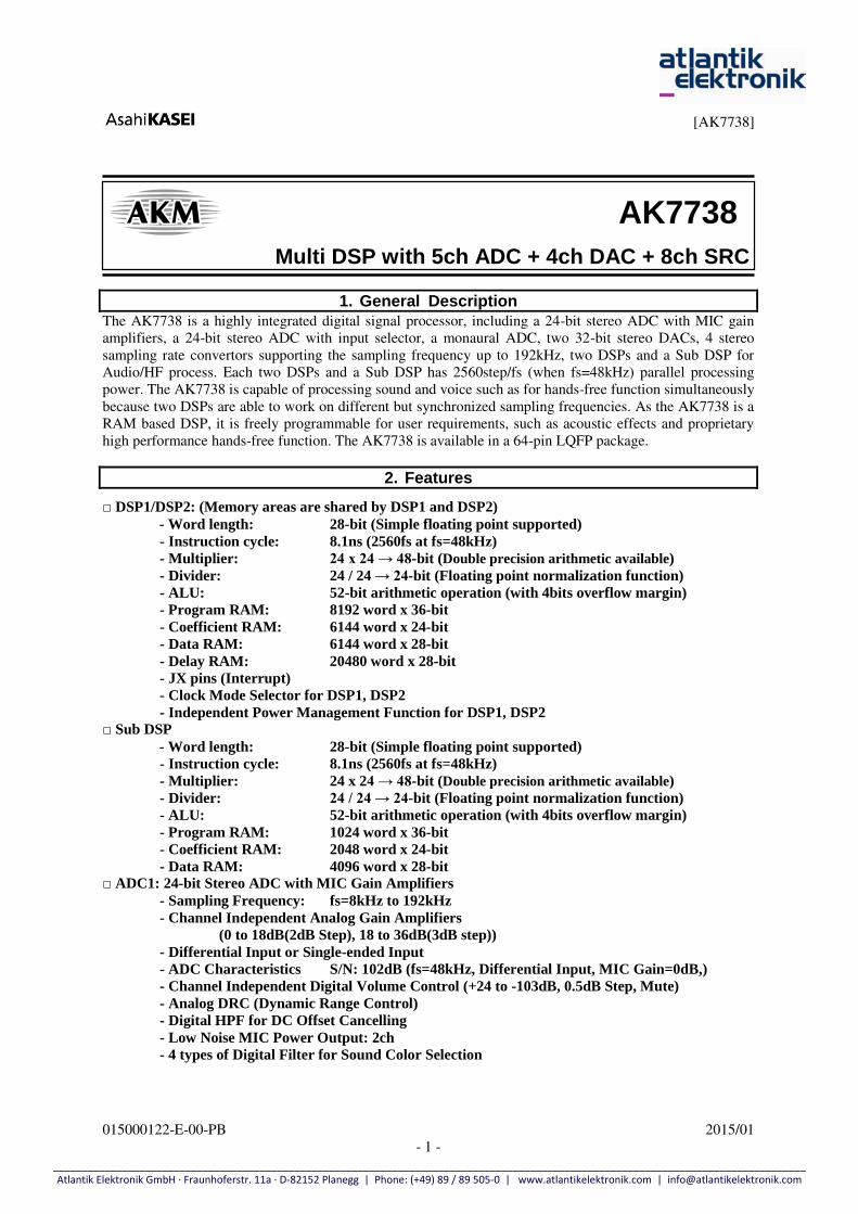
1. General Description The AK7738 is a highly integrated digital signal processor, including a 24-bit stereo ADC with MIC gain
amplifiers, a 24-bit stereo ADC with input selector, a monaural ADC, two 32-bit stereo DACs, 4 stereo
sampling rate convertors supporting the sampling frequency up to 192kHz, two DSPs and a Sub DSP for
Audio/HF process. Each two DSPs and a Sub DSP has 2560step/fs (when fs=48kHz) parallel processing
power. The AK7738 is capable of processing sound and voice such as for hands-free function simultaneously
because two DSPs are able to work on different but synchronized sampling frequencies. As the AK7738 is a
RAM based DSP, it is freely programmable for user requirements, such as acoustic effects and proprietary
high performance hands-free function. The AK7738 is available in a 64-pin LQFP package.
2. Features
□ DSP1/DSP2: (Memory areas are shared by DSP1 and DSP2)
- Word length: 28-bit (Simple floating point supported)
- Instruction cycle: 8.1ns (2560fs at fs=48kHz)
- Multiplier: 24 x 24 → 48-bit (Double precision arithmetic available)
- Divider: 24 / 24 → 24-bit (Floating point normalization function)
- ALU: 52-bit arithmetic operation (with 4bits overflow margin)
- Program RAM: 8192 word x 36-bit
- Coefficient RAM: 6144 word x 24-bit
- Data RAM: 6144 word x 28-bit
- Delay RAM: 20480 word x 28-bit
- JX pins (Interrupt)
- Clock Mode Selector for DSP1, DSP2
- Independent Power Management Function for DSP1, DSP2 □ Sub DSP
- Word length: 28-bit (Simple floating point supported)
- Instruction cycle: 8.1ns (2560fs at fs=48kHz)
- Multiplier: 24 x 24 → 48-bit (Double precision arithmetic available)
- Divider: 24 / 24 → 24-bit (Floating point normalization function)
- ALU: 52-bit arithmetic operation (with 4bits overflow margin)
- Program RAM: 1024 word x 36-bit
- Coefficient RAM: 2048 word x 24-bit
- Data RAM: 4096 word x 28-bit □ ADC1: 24-bit Stereo ADC with MIC Gain Amplifiers
- Sampling Frequency: fs=8kHz to 192kHz
- Channel Independent Analog Gain Amplifiers
(0 to 18dB(2dB Step), 18 to 36dB(3dB step))
- Differential Input or Single-ended Input
- ADC Characteristics S/N: 102dB (fs=48kHz, Differential Input, MIC Gain=0dB,)
- Channel Independent Digital Volume Control (+24 to -103dB, 0.5dB Step, Mute)
- Analog DRC (Dynamic Range Control)
- Digital HPF for DC Offset Cancelling
- Low Noise MIC Power Output: 2ch
- 4 types of Digital Filter for Sound Color Selection
Multi DSP with 5ch ADC + 4ch DAC + 8ch SRC
AK7738
___________________________________________________________________________________________________________________________________ Atlantik Elektronik GmbH ∙ Fraunhoferstr. 11a ∙ D-82152 Planegg | Phone: (+49) 89 / 89 505-0 | www.atlantikelektronik.com | [email protected]
[AK7738]
015000122-E-00-PB 2015/01
- 2 -
□ ADC2: 24-bit Stereo ADC with Input Selector
- Sampling Frequency: fs=8kHz to 192kHz
- Analog Input Selector: Differential Input x1 or Single-ended Input x2,
Semi-Differential Input x1
- ADC Characteristics S/N: 102dB (fs=48kHz, Differential Input)
- Channel Independent Digital Volume (+24 to -103dB, 0.5dB Step, Mute)
- Digital HPF for DC Offset Cancelling
- 4 types of Digital Filter for Sound Color Selection □ ADCM: 24-bit Monaural ADC
- Sampling Frequency: fs=8kHz to 192kHz
- Differential Input or Single-ended Input
- ADC Characteristics S/N: 102dB (fs=48kHz, Differential Input)
- Channel Independent Digital Volume (+24 to -103dB, 0.5dB Step, Mute)
- Digital HPF for DC Offset Cancelling
- 4 types of Digital Filter for Sound Color Selection □ DAC: Advanced 32-bit DAC
- 2ch x2
- Sampling Frequency: fs=8kHz to 192kHz
- Single-ended Output
- DAC Characteristics S/N: 108dB (fs=48kHz)
- Channel Independent Digital Volume Control (+12 to -115dB, 0.5dB Step, Mute)
- 4 types of Digital Filter for Sound Color Selection □ SRC:
- 2ch x4
- FSI = 8kHz to 192kHz, FSO = 8kHz to 192kHz (FSO/FSI = 0.167 to 6.0) □ FSCONV: Monaural Simple SRC
- 1ch x2
- FSI = 44.1kHz to 48kHz, FSO = 8kHz to 16kHz (FSO/FSI = 0.167 to 0.363) □ DIT:
- S/PDIF, IEC60958, AES/EBU, EIAJ CP1201 Compatible
- 24-bit Stereo Output
□ Digital Interface:
- Digital Input Port: max 24ch when TDM mode
- Digital Output Port: max 28ch when TDM mode
- Independent LRCK/BICK Input port x 5 Lines
- Data Format: MSB 32,24-bit / LSB 24,20,16-bit / I2S
- PCM Short / Long Frame Supported
- TDM Format Supported □ Digital Mixer Circuit
□ PLL Circuit
□ μP Interface: SPI(7MHz max), I2C-bus (1MHz, Fast Mode Plus)
□ Power Supply:
- Analog AVDD: 3.0 to 3.6V (typ. 3.3V)
- Digital LVDD: 3.0 to 3.6V (typ. 3.3V) (3.3V → 1.2V regulator integrated)
- I/F VDD33: 3.0 to 3.6V (typ. 3.3V)
TVDD1: 1.7 to 3.6V (typ. 3.3V)
TVDD2: 1.7 to 3.6V (typ. 3.3V)
□ Operating Temperature Range: -40C to 85C
□ Package: 64-pin LQFP (10mm x 10mm, 0.5mm pitch)
___________________________________________________________________________________________________________________________________ Atlantik Elektronik GmbH ∙ Fraunhoferstr. 11a ∙ D-82152 Planegg | Phone: (+49) 89 / 89 505-0 | www.atlantikelektronik.com | [email protected]
[AK7738]
015000122-E-00-PB 2015/01
- 3 -
3. Table of Contents 1. General Description ......................................................................................................................................... 1
2. Features ........................................................................................................................................................... 1
3. Table of Contents ............................................................................................................................................ 3
4. Block Diagram and Functions ......................................................................................................................... 4
■ Block Diagram .......................................................................................................................................... 4
■ DSP1 Block Diagram ............................................................................................................................... 5
■ DSP2 Block Diagram ............................................................................................................................... 6
■ Sub DSP Block Diagram .......................................................................................................................... 7
5. Pin Configurations and Functions ................................................................................................................... 8
■ Ordering Guide ......................................................................................................................................... 8
■ Pin Layout ................................................................................................................................................ 8
■ Pin Functions ............................................................................................................................................ 9
■ Handling of Unused Pins ........................................................................................................................ 12
■ Internal Pulled-down Pin Status ............................................................................................................. 12
■ Power-down Status of Output Pins ......................................................................................................... 13
■ Relationship between Power Supplies and Digital Pins ......................................................................... 13
6. Absolute Maximum Ratings .......................................................................................................................... 14
7. Recommended Operating Conditions ............................................................................................................ 14
8. Electrical Characteristics ............................................................................................................................... 15
■ Analog Characteristics ............................................................................................................................ 15
■ Power Consumption ............................................................................................................................... 20
9. Digital Filter Characteristics .......................................................................................................................... 21
10. DC Characteristics ......................................................................................................................................... 31
■ DC Characteristics .................................................................................................................................. 31
11. Switching Characteristics .............................................................................................................................. 32
12. Package .......................................................................................................................................................... 40
■ Outline Dimensions ................................................................................................................................ 40
■ Material and Lead Finish ........................................................................................................................ 40
■ Marking .................................................................................................................................................. 41
13. Revision History ............................................................................................................................................ 41
IMPORTANT NOTICE ...................................................................................................................................... 42
___________________________________________________________________________________________________________________________________ Atlantik Elektronik GmbH ∙ Fraunhoferstr. 11a ∙ D-82152 Planegg | Phone: (+49) 89 / 89 505-0 | www.atlantikelektronik.com | [email protected]
[AK7738]
015000122-E-00-PB 2015/01
- 4 -
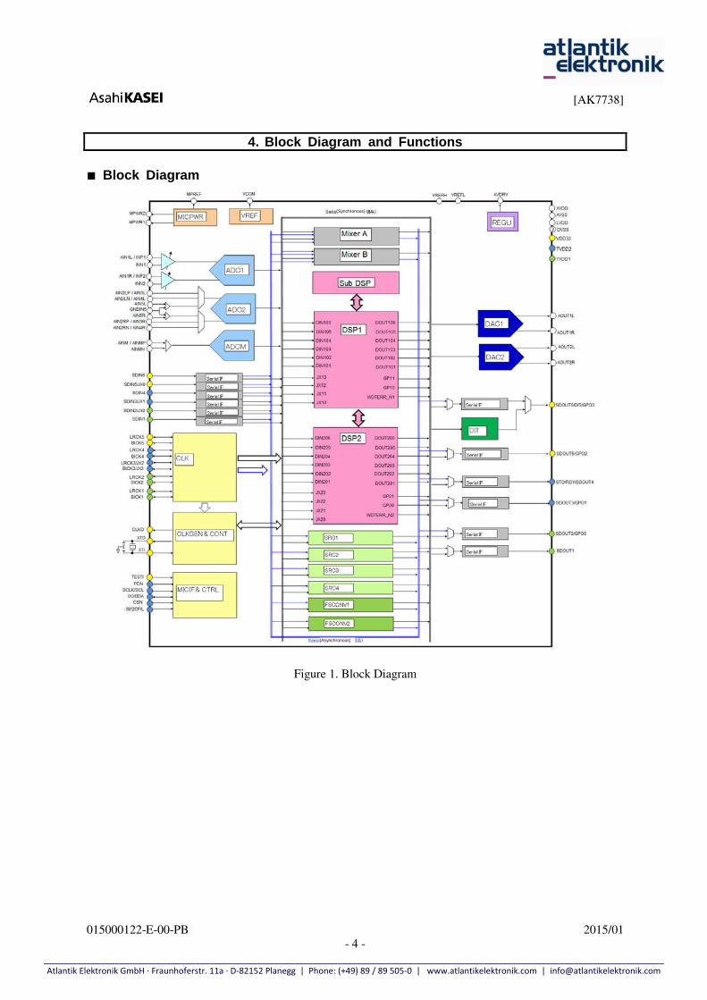
4. Block Diagram and Functions
■ Block Diagram
Figure 1. Block Diagram
(Synchronous)
(Asynchronous)
___________________________________________________________________________________________________________________________________ Atlantik Elektronik GmbH ∙ Fraunhoferstr. 11a ∙ D-82152 Planegg | Phone: (+49) 89 / 89 505-0 | www.atlantikelektronik.com | [email protected]
[AK7738]
015000122-E-00-PB 2015/01
- 5 -
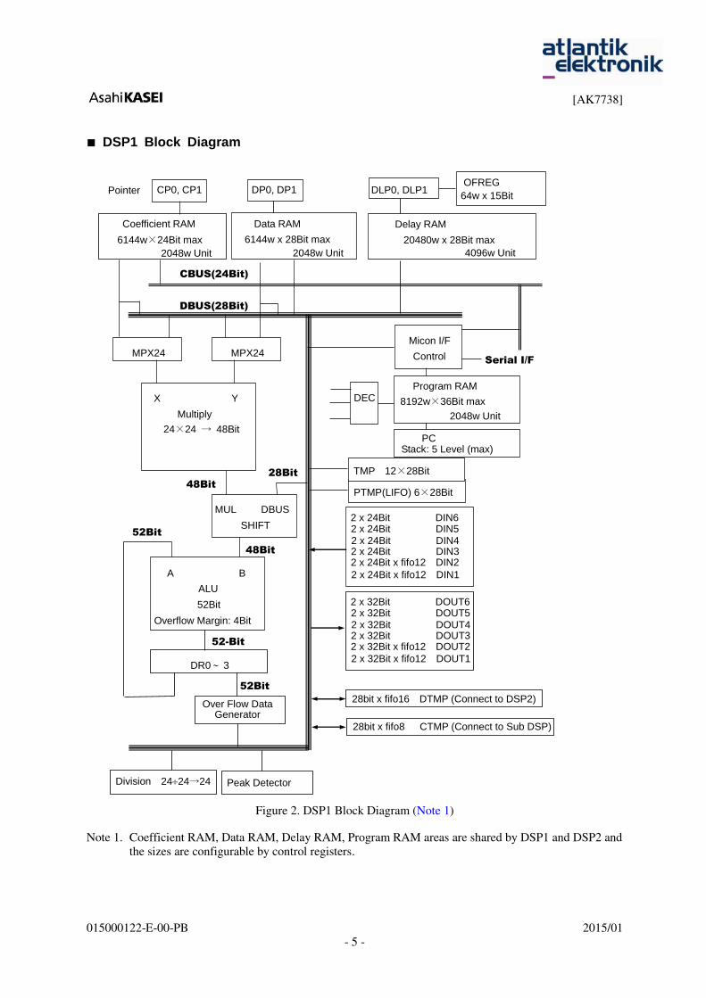
■ DSP1 Block Diagram
Figure 2. DSP1 Block Diagram (Note 1)
Note 1. Coefficient RAM, Data RAM, Delay RAM, Program RAM areas are shared by DSP1 and DSP2 and
the sizes are configurable by control registers.
×
CP0, CP1 DP0, DP1
Data RAM
6144w x 28Bit max
MPX24 MPX24
X Y
Multiply
24×24 → 48Bit
Micon I/F
Control
Program RAM
8192w×36Bit max DEC
PC Stack: 5 Level (max)
MUL DBUS
SHIFT
A B
ALU
52Bit
Overflow Margin: 4Bit
DR0 3
Over Flow Data Generator
Division 2424→24 Peak Detector
Serial I/F
CBUS(24Bit)
DBUS(28Bit)
48Bit 28Bit
48Bit
52Bit
52Bit
20480w x 28Bit max
PTMP(LIFO) 6×28Bit
DLP0, DLP1
52-Bit
TMP 12×28Bit
OFREG
64w x 15Bit
Delay RAM Coefficient RAM
6144w×24Bit max
Pointer
2048w Unit 2048w Unit 4096w Unit
2048w Unit
28bit x fifo16 DTMP (Connect to DSP2)
2 x 24Bit DIN6 2 x 24Bit DIN5 2 x 24Bit DIN4 2 x 24Bit DIN3 2 x 24Bit x fifo12 DIN2
2 x 24Bit x fifo12 DIN1
2 x 32Bit DOUT6 2 x 32Bit DOUT5 2 x 32Bit DOUT4 2 x 32Bit DOUT3 2 x 32Bit x fifo12 DOUT2 2 x 32Bit x fifo12 DOUT1
28bit x fifo8 CTMP (Connect to Sub DSP)
[AK7738]
015000122-E-00-PB 2015/01
- 6 -
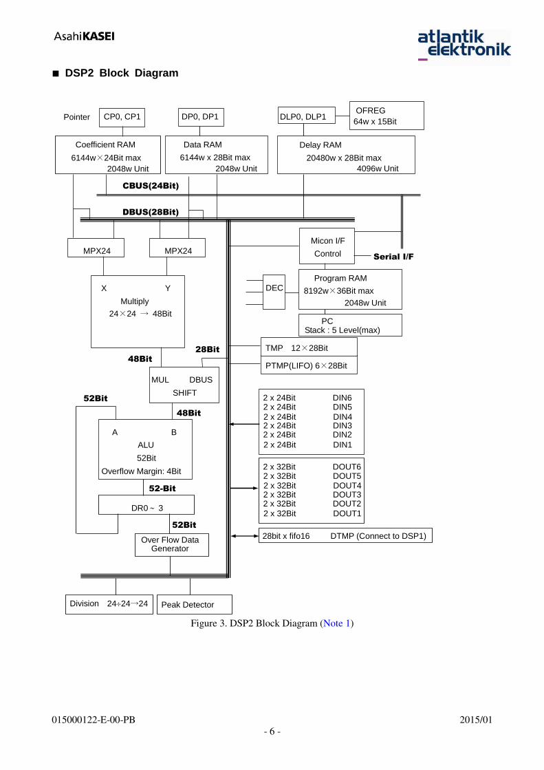
■ DSP2 Block Diagram
Figure 3. DSP2 Block Diagram (Note 1)
×
CP0, CP1 DP0, DP1
Data RAM
6144w x 28Bit max
MPX24 MPX24
X Y
Multiply
24×24 → 48Bit
Micon I/F
Control
Program RAM
8192w×36Bit max DEC
PC Stack : 5 Level(max)
MUL DBUS
SHIFT
A B
ALU
52Bit
Overflow Margin: 4Bit
DR0 3
Over Flow Data Generator
Division 2424→24 Peak Detector
Serial I/F
CBUS(24Bit)
DBUS(28Bit)
48Bit 28Bit
48Bit
52Bit
52Bit
20480w x 28Bit max
PTMP(LIFO) 6×28Bit
DLP0, DLP1
52-Bit
TMP 12×28Bit
OFREG
64w x 15Bit
Delay RAM Coefficient RAM
6144w×24Bit max
Pointer
2048w Unit 2048w Unit 4096w Unit
2048w Unit
28bit x fifo16 DTMP (Connect to DSP1)
2 x 24Bit DIN6 2 x 24Bit DIN5 2 x 24Bit DIN4 2 x 24Bit DIN3 2 x 24Bit DIN2
2 x 24Bit DIN1
2 x 32Bit DOUT6 2 x 32Bit DOUT5 2 x 32Bit DOUT4 2 x 32Bit DOUT3 2 x 32Bit DOUT2 2 x 32Bit DOUT1
[AK7738]
015000122-E-00-PB 2015/01
- 7 -
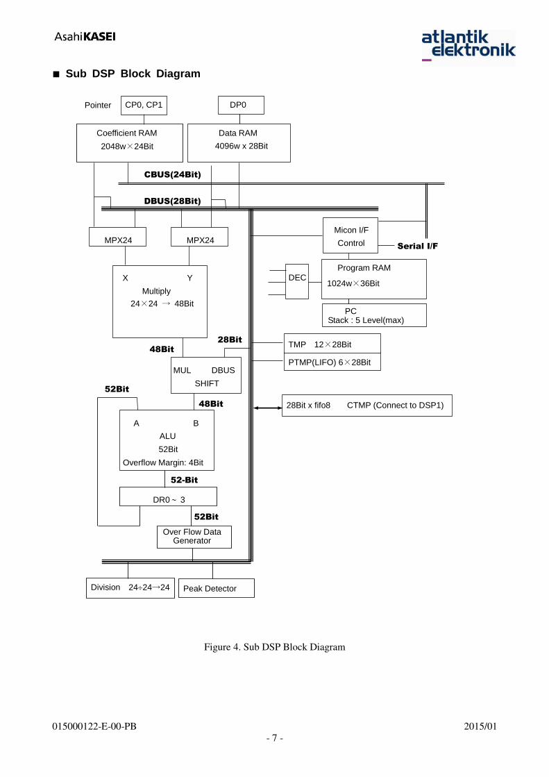
■ Sub DSP Block Diagram
Figure 4. Sub DSP Block Diagram
×
CP0, CP1 DP0
Data RAM
4096w x 28Bit
MPX24 MPX24
X Y
Multiply
24×24 → 48Bit
Micon I/F
Control
Program RAM
1024w×36Bit DEC
PC Stack : 5 Level(max)
MUL DBUS
SHIFT
A B
ALU
52Bit
Overflow Margin: 4Bit
DR0 3
Over Flow Data Generator
Peak Detector
Serial I/F
CBUS(24Bit)
DBUS(28Bit)
48Bit 28Bit
48Bit
52Bit
52Bit
PTMP(LIFO) 6×28Bit
52-Bit
TMP 12×28Bit
Coefficient RAM
2048w×24Bit
Pointer
28Bit x fifo8 CTMP (Connect to DSP1)
Division 2424→24
[AK7738]
015000122-E-00-PB 2015/01
- 8 -
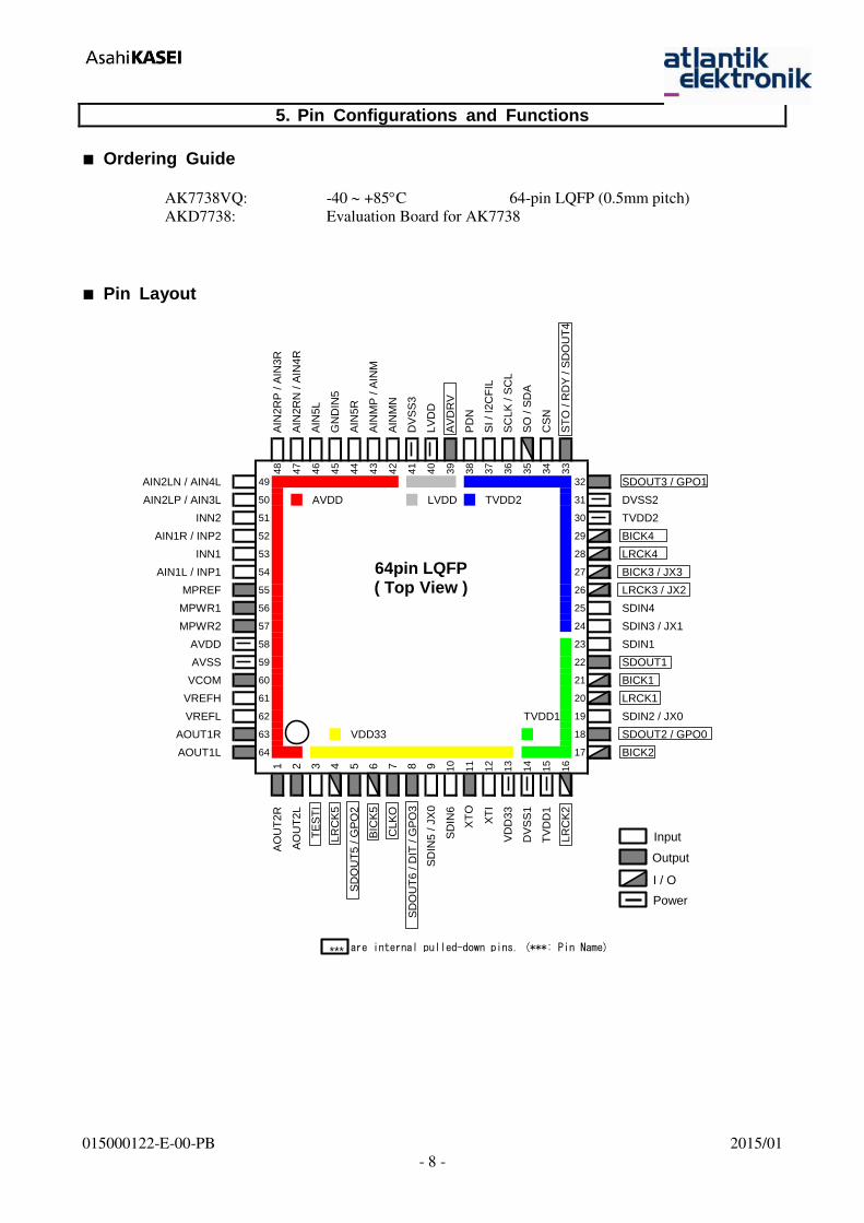
5. Pin Configurations and Functions
■ Ordering Guide
AK7738VQ: -40 +85C 64-pin LQFP (0.5mm pitch)
AKD7738: Evaluation Board for AK7738
■ Pin Layout
AIN
2R
P / A
IN3R
AIN
2R
N / A
IN4R
AIN
5L
GN
DIN
5
AIN
5R
AIN
MP
/ A
INM
AIN
MN
DV
SS
3
LV
DD
AV
DR
V
PD
N
SI / I2
CF
IL
SC
LK
/ S
CL
SO
/ S
DA
CS
N
ST
O / R
DY
/ S
DO
UT
4
48
47
46
45
44
43
42
41
40
39
38
37
36
35
34
33
AIN2LN / AIN4L 49 32 SDOUT3 / GPO1
AIN2LP / AIN3L 50 AVDD LVDD TVDD2 31 DVSS2
INN2 51 30 TVDD2
AIN1R / INP2 52 29 BICK4
INN1 53 28 LRCK4
AIN1L / INP1 54 27 BICK3 / JX3
MPREF 55 26 LRCK3 / JX2
MPWR1 56 25 SDIN4
MPWR2 57 24 SDIN3 / JX1
AVDD 58 23 SDIN1
AVSS 59 22 SDOUT1
VCOM 60 21 BICK1
VREFH 61 20 LRCK1
VREFL 62 TVDD1 19 SDIN2 / JX0
AOUT1R 63 VDD33 18 SDOUT2 / GPO0
AOUT1L 64 17 BICK2
1 2 3 4 5 6 7 8 9 10
11
12
13
14
15
16
AO
UT
2R
AO
UT
2L
TE
ST
I
LR
CK
5
SD
OU
T5 / G
PO
2
BIC
K5
CLK
O
SD
IN6
XT
I
VD
D33
DV
SS
1
TV
DD
1
LR
CK
2
are internal pulled-down pins. (***: Pin Name)
64pin LQFP( Top View )
Input
Output
I / O
Power
***
SD
IN5 /
JX
0
XT
O
SD
OU
T6 / D
IT / G
PO
3
[AK7738]
015000122-E-00-PB 2015/01
- 9 -
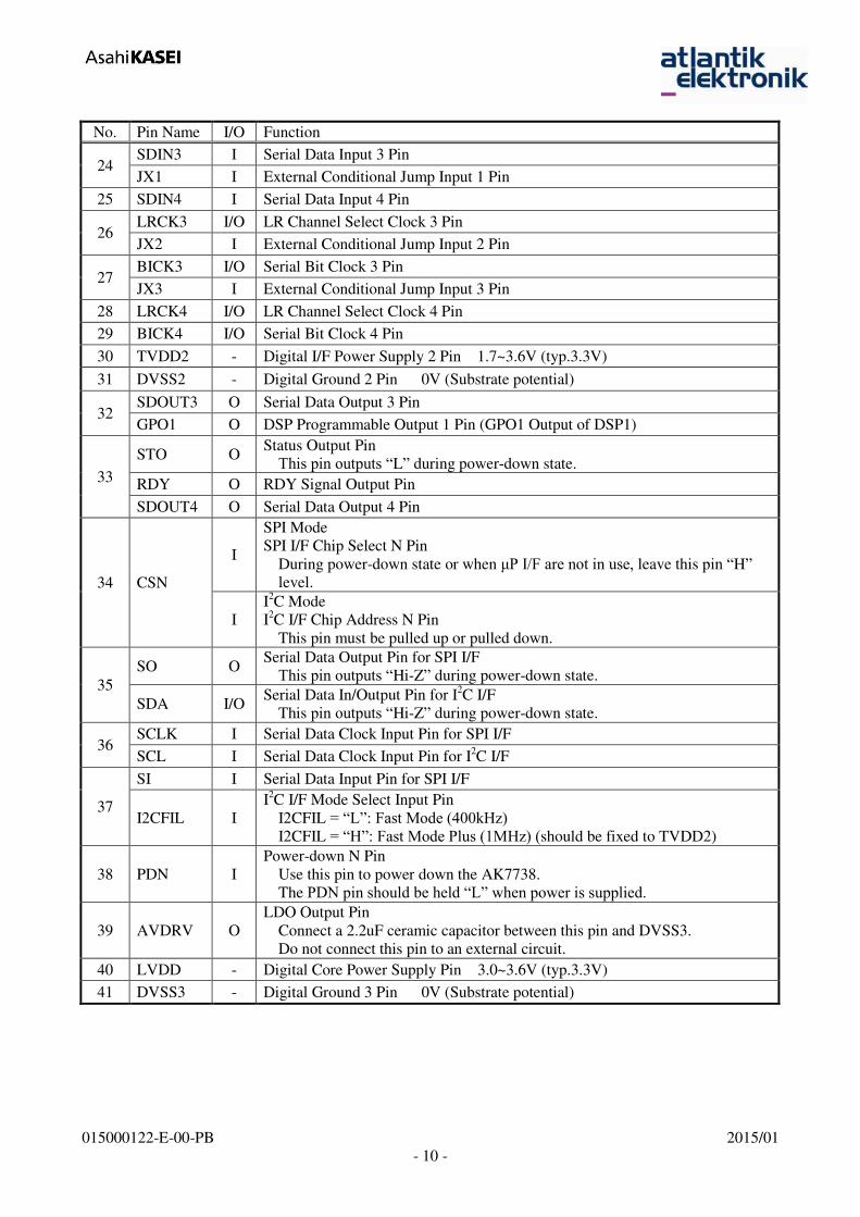
■ Pin Functions
No. Pin Name I/O Function
1 AOUT2R O DAC2 Rch Analog Output Pin
This pin outputs “Hi-Z” during power-down state.
2 AOUT2L O DAC2 Lch Analog Output Pin
This pin outputs “Hi-Z” during power-down state.
3 TESTI I Test Input Pin
It must be tied “L”.
4 LRCK5 I/O LR Channel Select Clock 5 Pin
5 SDOUT5 O Serial Data Output 5 Pin
GPO2 O DSP Programmable Output 2 Pin (GPO0 Output of DSP2)
6 BICK5 I/O Serial Bit Clock 5 Pin
7 CLKO O Master Clock Output Pin
8
SDOUT6 O Serial Data Output 6 Pin
DIT O Digital Transmit Channel Output Pin
GPO3 O DSP Programmable Output 3 Pin (GPO1 Output of DSP2)
9 SDIN5 I Serial Data Input 5 Pin
JX0 I External Conditional Jump Input 0 Pin
10 SDIN6 I Serial Data Input 6 Pin
11 XTO O
Crystal Oscillator Output Pin
When using a crystal oscillator, connect it between XTI and XTO.
When not using a crystal oscillator, leave this pin open.
12 XTI I
Crystal Oscillator Input Pin
When using a crystal oscillator, connect it between XTI and XTO.
When not using a crystal oscillator, connect this pin to an external clock or
DVSS1.
13 VDD33 - Digital I/F Power Supply Pin 3.0~3.6V (typ.3.3V)
14 DVSS1 - Digital Ground 1 Pin 0V (Substrate potential)
15 TVDD1 - Digital I/F Power Supply 1 Pin 1.7~3.6V (typ.3.3V)
16 LRCK2 I/O LR Channel Select Clock 2 Pin
17 BICK2 I/O Serial Bit Clock 2 Pin
18 SDOUT2 O Serial Data Output 2 Pin
GPO0 O DSP Programmable Output 0 Pin (GPO0 Output of DSP1)
19 SDIN2 I Serial Data Input 2 Pin
JX0 I External Conditional Jump Input 0 Pin
20 LRCK1 I/O LR Channel Select Clock 1 Pin
21 BICK1 I/O Serial Bit Clock 1 Pin
22 SDOUT1 O Serial Data Output 1 Pin
23 SDIN1 I Serial Data Input 1 Pin
[AK7738]
015000122-E-00-PB 2015/01
- 10 -
No. Pin Name I/O Function
24 SDIN3 I Serial Data Input 3 Pin
JX1 I External Conditional Jump Input 1 Pin
25 SDIN4 I Serial Data Input 4 Pin
26 LRCK3 I/O LR Channel Select Clock 3 Pin
JX2 I External Conditional Jump Input 2 Pin
27 BICK3 I/O Serial Bit Clock 3 Pin
JX3 I External Conditional Jump Input 3 Pin
28 LRCK4 I/O LR Channel Select Clock 4 Pin
29 BICK4 I/O Serial Bit Clock 4 Pin
30 TVDD2 - Digital I/F Power Supply 2 Pin 1.7~3.6V (typ.3.3V)
31 DVSS2 - Digital Ground 2 Pin 0V (Substrate potential)
32 SDOUT3 O Serial Data Output 3 Pin
GPO1 O DSP Programmable Output 1 Pin (GPO1 Output of DSP1)
33
STO O Status Output Pin
This pin outputs “L” during power-down state.
RDY O RDY Signal Output Pin
SDOUT4 O Serial Data Output 4 Pin
34 CSN
I
SPI Mode
SPI I/F Chip Select N Pin
During power-down state or when μP I/F are not in use, leave this pin “H”
level.
I
I2C Mode
I2C I/F Chip Address N Pin
This pin must be pulled up or pulled down.
35
SO O Serial Data Output Pin for SPI I/F
This pin outputs “Hi-Z” during power-down state.
SDA I/O Serial Data In/Output Pin for I
2C I/F
This pin outputs “Hi-Z” during power-down state.
36 SCLK I Serial Data Clock Input Pin for SPI I/F
SCL I Serial Data Clock Input Pin for I2C I/F
37
SI I Serial Data Input Pin for SPI I/F
I2CFIL I
I2C I/F Mode Select Input Pin
I2CFIL = “L”: Fast Mode (400kHz) I2CFIL = “H”: Fast Mode Plus (1MHz) (should be fixed to TVDD2)
38 PDN I
Power-down N Pin
Use this pin to power down the AK7738.
The PDN pin should be held “L” when power is supplied.
39 AVDRV O
LDO Output Pin
Connect a 2.2uF ceramic capacitor between this pin and DVSS3.
Do not connect this pin to an external circuit.
40 LVDD - Digital Core Power Supply Pin 3.0~3.6V (typ.3.3V)
41 DVSS3 - Digital Ground 3 Pin 0V (Substrate potential)
[AK7738]
015000122-E-00-PB 2015/01
- 11 -
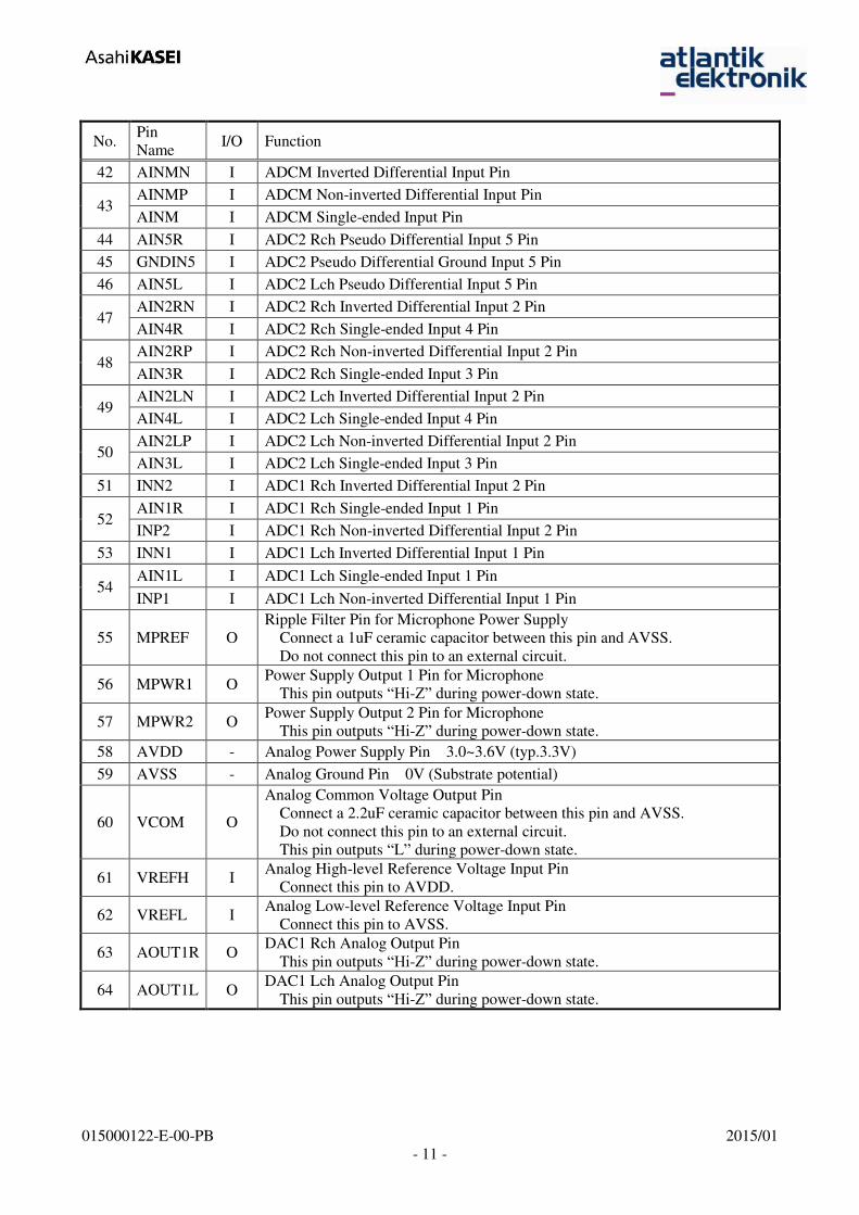
No. Pin
Name I/O Function
42 AINMN I ADCM Inverted Differential Input Pin
43 AINMP I ADCM Non-inverted Differential Input Pin
AINM I ADCM Single-ended Input Pin
44 AIN5R I ADC2 Rch Pseudo Differential Input 5 Pin
45 GNDIN5 I ADC2 Pseudo Differential Ground Input 5 Pin
46 AIN5L I ADC2 Lch Pseudo Differential Input 5 Pin
47 AIN2RN I ADC2 Rch Inverted Differential Input 2 Pin
AIN4R I ADC2 Rch Single-ended Input 4 Pin
48 AIN2RP I ADC2 Rch Non-inverted Differential Input 2 Pin
AIN3R I ADC2 Rch Single-ended Input 3 Pin
49 AIN2LN I ADC2 Lch Inverted Differential Input 2 Pin
AIN4L I ADC2 Lch Single-ended Input 4 Pin
50 AIN2LP I ADC2 Lch Non-inverted Differential Input 2 Pin
AIN3L I ADC2 Lch Single-ended Input 3 Pin
51 INN2 I ADC1 Rch Inverted Differential Input 2 Pin
52 AIN1R I ADC1 Rch Single-ended Input 1 Pin
INP2 I ADC1 Rch Non-inverted Differential Input 2 Pin
53 INN1 I ADC1 Lch Inverted Differential Input 1 Pin
54 AIN1L I ADC1 Lch Single-ended Input 1 Pin
INP1 I ADC1 Lch Non-inverted Differential Input 1 Pin
55 MPREF O
Ripple Filter Pin for Microphone Power Supply
Connect a 1uF ceramic capacitor between this pin and AVSS.
Do not connect this pin to an external circuit.
56 MPWR1 O Power Supply Output 1 Pin for Microphone
This pin outputs “Hi-Z” during power-down state.
57 MPWR2 O Power Supply Output 2 Pin for Microphone
This pin outputs “Hi-Z” during power-down state.
58 AVDD - Analog Power Supply Pin 3.0~3.6V (typ.3.3V)
59 AVSS - Analog Ground Pin 0V (Substrate potential)
60 VCOM O
Analog Common Voltage Output Pin
Connect a 2.2uF ceramic capacitor between this pin and AVSS.
Do not connect this pin to an external circuit.
This pin outputs “L” during power-down state.
61 VREFH I Analog High-level Reference Voltage Input Pin
Connect this pin to AVDD.
62 VREFL I Analog Low-level Reference Voltage Input Pin
Connect this pin to AVSS.
63 AOUT1R O DAC1 Rch Analog Output Pin
This pin outputs “Hi-Z” during power-down state.
64 AOUT1L O DAC1 Lch Analog Output Pin
This pin outputs “Hi-Z” during power-down state.
[AK7738]
015000122-E-00-PB 2015/01
- 12 -
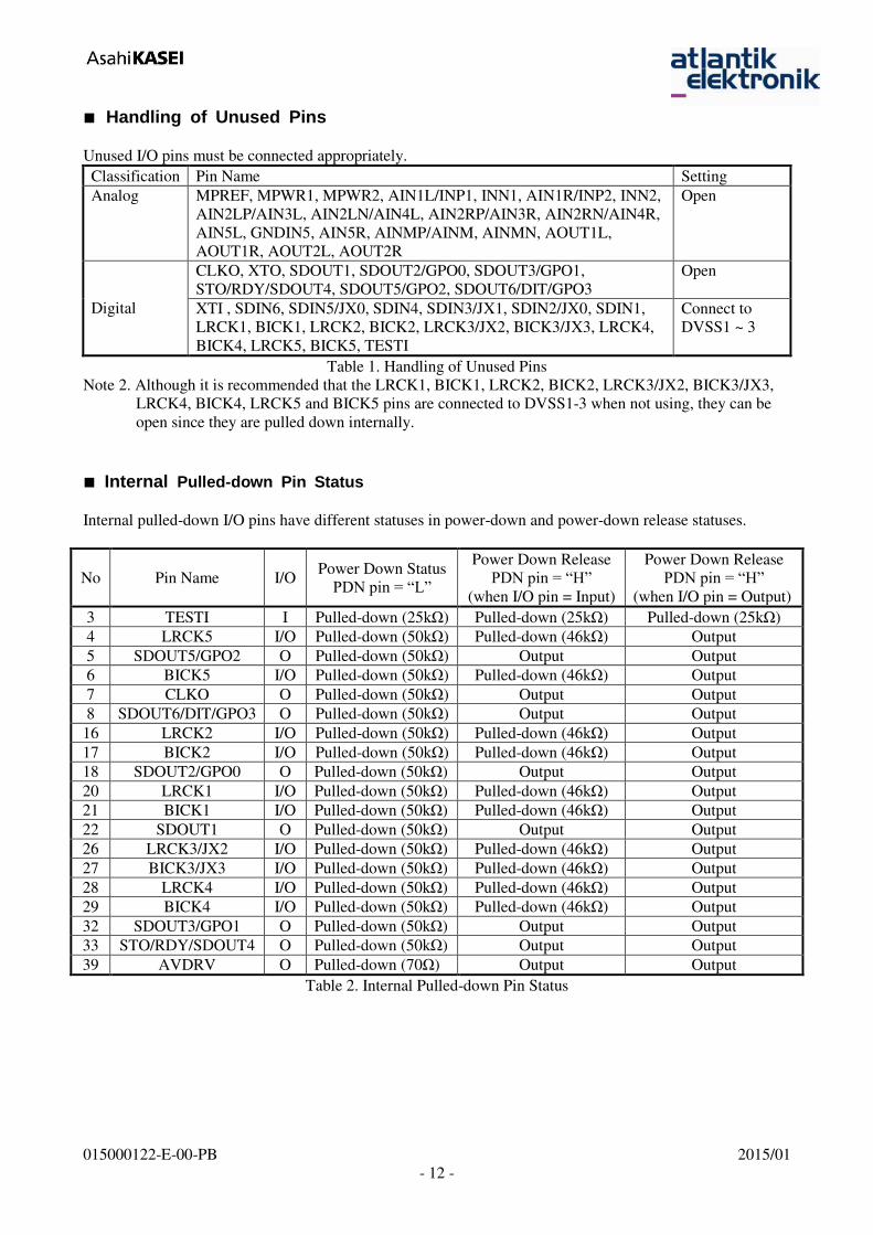
■ Handling of Unused Pins
Unused I/O pins must be connected appropriately.
Classification Pin Name Setting
Analog MPREF, MPWR1, MPWR2, AIN1L/INP1, INN1, AIN1R/INP2, INN2,
AIN2LP/AIN3L, AIN2LN/AIN4L, AIN2RP/AIN3R, AIN2RN/AIN4R,
AIN5L, GNDIN5, AIN5R, AINMP/AINM, AINMN, AOUT1L,
AOUT1R, AOUT2L, AOUT2R
Open
Digital
CLKO, XTO, SDOUT1, SDOUT2/GPO0, SDOUT3/GPO1,
STO/RDY/SDOUT4, SDOUT5/GPO2, SDOUT6/DIT/GPO3
Open
XTI , SDIN6, SDIN5/JX0, SDIN4, SDIN3/JX1, SDIN2/JX0, SDIN1,
LRCK1, BICK1, LRCK2, BICK2, LRCK3/JX2, BICK3/JX3, LRCK4,
BICK4, LRCK5, BICK5, TESTI
Connect to
DVSS1 ~ 3
Table 1. Handling of Unused Pins
Note 2. Although it is recommended that the LRCK1, BICK1, LRCK2, BICK2, LRCK3/JX2, BICK3/JX3,
LRCK4, BICK4, LRCK5 and BICK5 pins are connected to DVSS1-3 when not using, they can be
open since they are pulled down internally.
■ Internal Pulled-down Pin Status
Internal pulled-down I/O pins have different statuses in power-down and power-down release statuses.
No Pin Name I/O Power Down Status
PDN pin = “L”
Power Down Release
PDN pin = “H”
(when I/O pin = Input)
Power Down Release
PDN pin = “H”
(when I/O pin = Output)
3 TESTI I Pulled-down (25kΩ) Pulled-down (25kΩ) Pulled-down (25kΩ)
4 LRCK5 I/O Pulled-down (50kΩ) Pulled-down (46kΩ) Output
5 SDOUT5/GPO2 O Pulled-down (50kΩ) Output Output
6 BICK5 I/O Pulled-down (50kΩ) Pulled-down (46kΩ) Output
7 CLKO O Pulled-down (50kΩ) Output Output
8 SDOUT6/DIT/GPO3 O Pulled-down (50kΩ) Output Output
16 LRCK2 I/O Pulled-down (50kΩ) Pulled-down (46kΩ) Output
17 BICK2 I/O Pulled-down (50kΩ) Pulled-down (46kΩ) Output
18 SDOUT2/GPO0 O Pulled-down (50kΩ) Output Output
20 LRCK1 I/O Pulled-down (50kΩ) Pulled-down (46kΩ) Output
21 BICK1 I/O Pulled-down (50kΩ) Pulled-down (46kΩ) Output
22 SDOUT1 O Pulled-down (50kΩ) Output Output
26 LRCK3/JX2 I/O Pulled-down (50kΩ) Pulled-down (46kΩ) Output
27 BICK3/JX3 I/O Pulled-down (50kΩ) Pulled-down (46kΩ) Output
28 LRCK4 I/O Pulled-down (50kΩ) Pulled-down (46kΩ) Output
29 BICK4 I/O Pulled-down (50kΩ) Pulled-down (46kΩ) Output
32 SDOUT3/GPO1 O Pulled-down (50kΩ) Output Output
33 STO/RDY/SDOUT4 O Pulled-down (50kΩ) Output Output
39 AVDRV O Pulled-down (70Ω) Output Output
Table 2. Internal Pulled-down Pin Status
[AK7738]
015000122-E-00-PB 2015/01
- 13 -
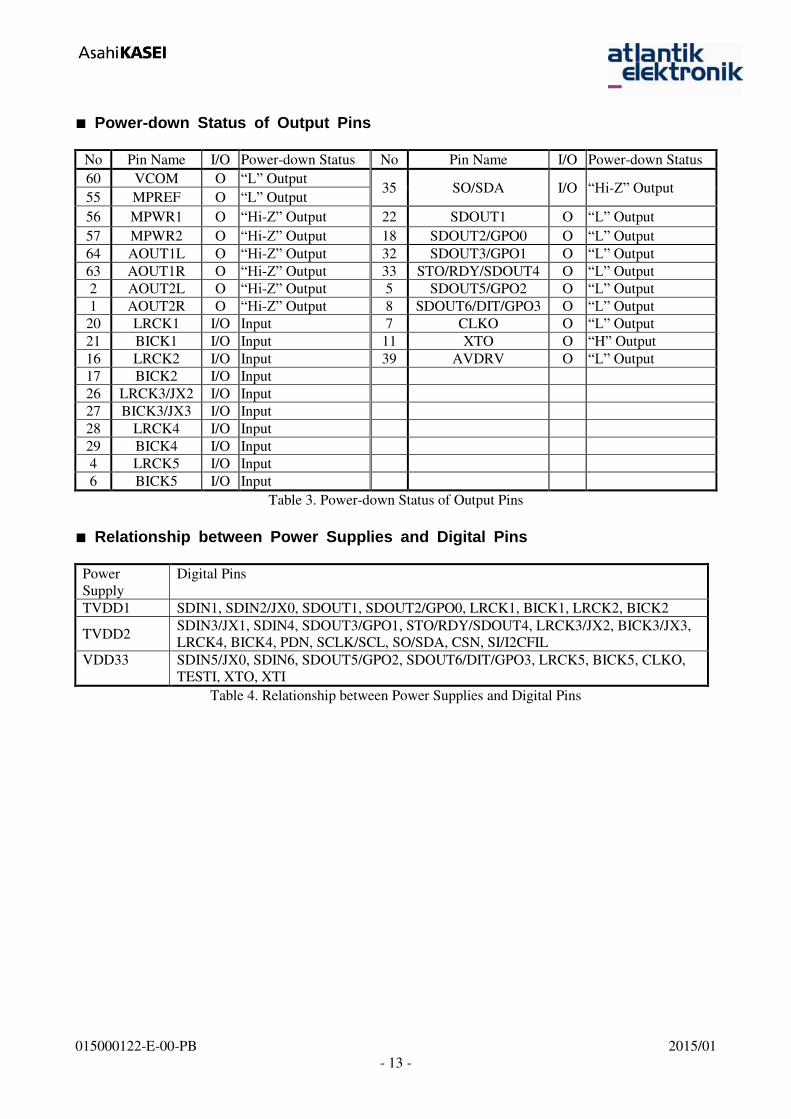
■ Power-down Status of Output Pins
No Pin Name I/O Power-down Status No Pin Name I/O Power-down Status
60 VCOM O “L” Output 35 SO/SDA I/O “Hi-Z” Output
55 MPREF O “L” Output
56 MPWR1 O “Hi-Z” Output 22 SDOUT1 O “L” Output
57 MPWR2 O “Hi-Z” Output 18 SDOUT2/GPO0 O “L” Output
64 AOUT1L O “Hi-Z” Output 32 SDOUT3/GPO1 O “L” Output
63 AOUT1R O “Hi-Z” Output 33 STO/RDY/SDOUT4 O “L” Output
2 AOUT2L O “Hi-Z” Output 5 SDOUT5/GPO2 O “L” Output
1 AOUT2R O “Hi-Z” Output 8 SDOUT6/DIT/GPO3 O “L” Output
20 LRCK1 I/O Input 7 CLKO O “L” Output
21 BICK1 I/O Input 11 XTO O “H” Output
16 LRCK2 I/O Input 39 AVDRV O “L” Output
17 BICK2 I/O Input
26 LRCK3/JX2 I/O Input
27 BICK3/JX3 I/O Input
28 LRCK4 I/O Input
29 BICK4 I/O Input
4 LRCK5 I/O Input
6 BICK5 I/O Input
Table 3. Power-down Status of Output Pins
■ Relationship between Power Supplies and Digital Pins
Power
Supply
Digital Pins
TVDD1 SDIN1, SDIN2/JX0, SDOUT1, SDOUT2/GPO0, LRCK1, BICK1, LRCK2, BICK2
TVDD2 SDIN3/JX1, SDIN4, SDOUT3/GPO1, STO/RDY/SDOUT4, LRCK3/JX2, BICK3/JX3,
LRCK4, BICK4, PDN, SCLK/SCL, SO/SDA, CSN, SI/I2CFIL
VDD33 SDIN5/JX0, SDIN6, SDOUT5/GPO2, SDOUT6/DIT/GPO3, LRCK5, BICK5, CLKO,
TESTI, XTO, XTI
Table 4. Relationship between Power Supplies and Digital Pins
[AK7738]
015000122-E-00-PB 2015/01
- 14 -
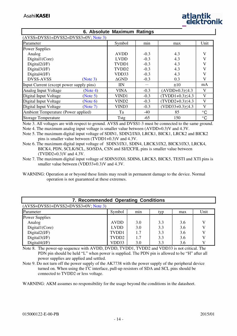
6. Absolute Maximum Ratings (AVSS=DVSS1=DVSS2=DVSS3=0V; Note 3)
Parameter Symbol min max Unit
Power Supplies
Analog
Digital1(Core)
Digital2(I/F)
Digital3(I/F)
Digital4(I/F)
DVSS-AVSS (Note 3)
AVDD
LVDD
TVDD1
TVDD2
VDD33
ΔGND
-0.3
-0.3
-0.3
-0.3
-0.3
-0.3
4.3
4.3
4.3
4.3
4.3
0.3
V
V
V
V
V
V
Input Current (except power supply pins) IIN - ±10 mA
Analog Input Voltage (Note 4) VINA -0.3 (AVDD+0.3)≤4.3 V
Digital Input Voltage (Note 5) VIND1 -0.3 (TVDD1+0.3)≤4.3 V
Digital Input Voltage (Note 6) VIND2 -0.3 (TVDD2+0.3)≤4.3 V
Digital Input Voltage (Note 7) VIND3 -0.3 (VDD33+0.3)≤4.3 V
Ambient Temperature (Power applied) Ta -40 85 C
Storage Temperature Tstg -65 150 C
Note 3. All voltages are with respect to ground. AVSS and DVSS1-3 must be connected to the same ground.
Note 4. The maximum analog input voltage is smaller value between (AVDD+0.3)V and 4.3V.
Note 5. The maximum digital input voltage of SDIN1, SDIN2/JX0, LRCK1, BICK1, LRCK2 and BICK2
pins is smaller value between (TVDD1+0.3)V and 4.3V.
Note 6. The maximum digital input voltage of SDIN3/JX1, SDIN4, LRCK3/JX2, BICK3/JX3, LRCK4,
BICK4, PDN, SCLK/SCL, SO/SDA, CSN and SI/I2CFIL pins is smaller value between
(TVDD2+0.3)V and 4.3V.
Note 7. The maximum digital input voltage of SDIN5/JX0, SDIN6, LRCK5, BICK5, TESTI and XTI pins is
smaller value between (VDD33+0.3)V and 4.3V.
WARNING: Operation at or beyond these limits may result in permanent damage to the device. Normal
operation is not guaranteed at these extremes.
7. Recommended Operating Conditions (AVSS=DVSS1=DVSS2=DVSS3=0V; Note 3)
Parameter Symbol min typ max Unit
Power Supplies
Analog
Digital1(Core)
Digital2(I/F)
Digital3(I/F)
Digital4(I/F)
AVDD
LVDD
TVDD1
TVDD2
VDD33
3.0
3.0
1.7
1.7
3.0
3.3
3.3
3.3
3.3
3.3
3.6
3.6
3.6
3.6
3.6
V
V
V
V
V
Note 8. The power-up sequence with AVDD, DVDD, TVDD1, TVDD2 and VDD33 is not critical. The
PDN pin should be held “L” when power is supplied. The PDN pin is allowed to be “H” after all power supplies are applied and settled.
Note 9. Do not turn off the power supply of the AK7738 with the power supply of the peripheral device
turned on. When using the I2C interface, pull-up resistors of SDA and SCL pins should be
connected to TVDD2 or less voltage.
WARNING: AKM assumes no responsibility for the usage beyond the conditions in the datasheet.
[AK7738]
015000122-E-00-PB 2015/01
- 15 -
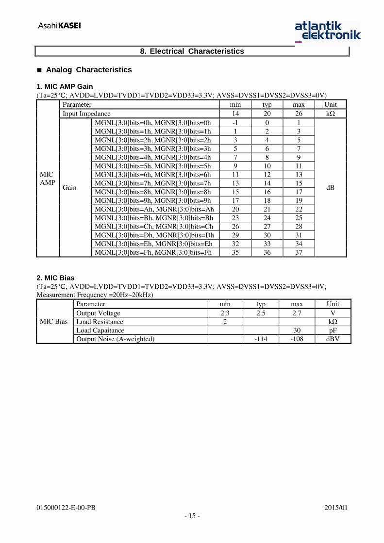
8. Electrical Characteristics
■ Analog Characteristics
1. MIC AMP Gain
(Ta=25C; AVDD=LVDD=TVDD1=TVDD2=VDD33=3.3V; AVSS=DVSS1=DVSS2=DVSS3=0V)
MIC
AMP
Parameter min typ max Unit
Input Impedance 14 20 26 kΩ
Gain
MGNL[3:0]bits=0h, MGNR[3:0]bits=0h -1 0 1
dB
MGNL[3:0]bits=1h, MGNR[3:0]bits=1h 1 2 3
MGNL[3:0]bits=2h, MGNR[3:0]bits=2h 3 4 5
MGNL[3:0]bits=3h, MGNR[3:0]bits=3h 5 6 7
MGNL[3:0]bits=4h, MGNR[3:0]bits=4h 7 8 9
MGNL[3:0]bits=5h, MGNR[3:0]bits=5h 9 10 11
MGNL[3:0]bits=6h, MGNR[3:0]bits=6h 11 12 13
MGNL[3:0]bits=7h, MGNR[3:0]bits=7h 13 14 15
MGNL[3:0]bits=8h, MGNR[3:0]bits=8h 15 16 17
MGNL[3:0]bits=9h, MGNR[3:0]bits=9h 17 18 19
MGNL[3:0]bits=Ah, MGNR[3:0]bits=Ah 20 21 22
MGNL[3:0]bits=Bh, MGNR[3:0]bits=Bh 23 24 25
MGNL[3:0]bits=Ch, MGNR[3:0]bits=Ch 26 27 28
MGNL[3:0]bits=Dh, MGNR[3:0]bits=Dh 29 30 31
MGNL[3:0]bits=Eh, MGNR[3:0]bits=Eh 32 33 34
MGNL[3:0]bits=Fh, MGNR[3:0]bits=Fh 35 36 37
2. MIC Bias
(Ta=25C; AVDD=LVDD=TVDD1=TVDD2=VDD33=3.3V; AVSS=DVSS1=DVSS2=DVSS3=0V;
Measurement Frequency =20Hz~20kHz)
MIC Bias
Parameter min typ max Unit
Output Voltage 2.3 2.5 2.7 V
Load Resistance 2 kΩ
Load Capaitance 30 pF
Output Noise (A-weighted) -114 -108 dBV
[AK7738]
015000122-E-00-PB 2015/01
- 16 -
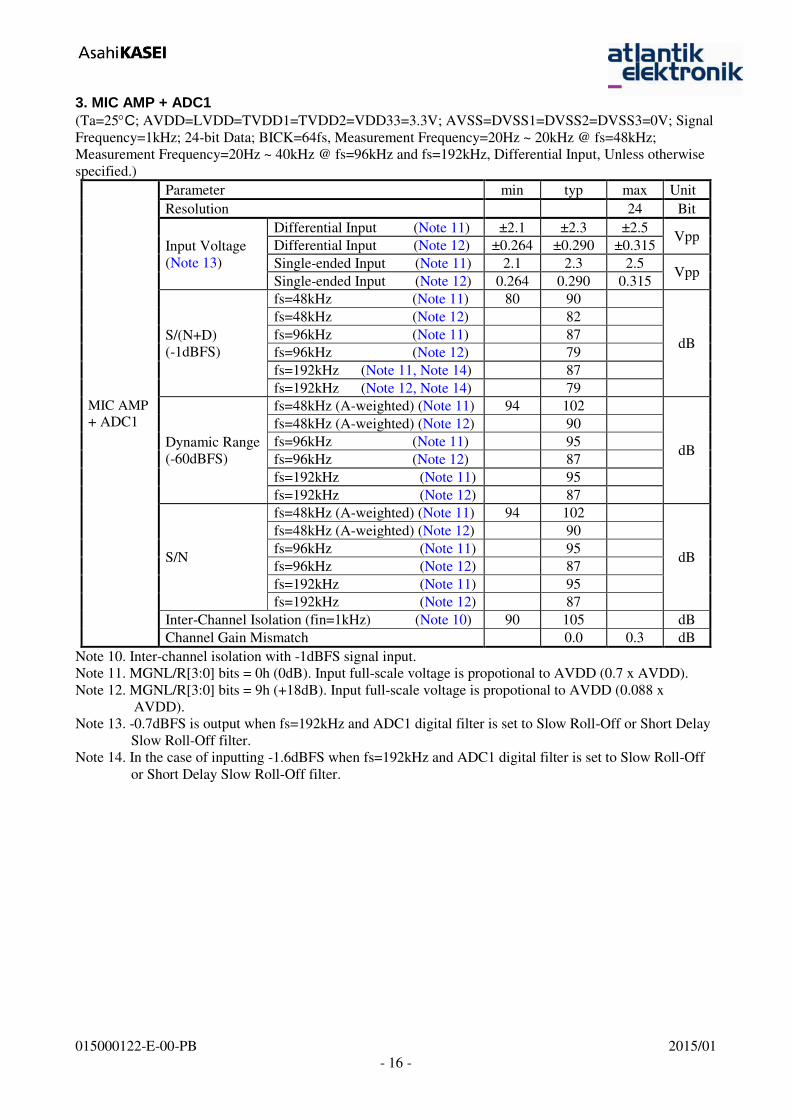
3. MIC AMP + ADC1 (Ta=25C; AVDD=LVDD=TVDD1=TVDD2=VDD33=3.3V; AVSS=DVSS1=DVSS2=DVSS3=0V; Signal
Frequency=1kHz; 24-bit Data; BICK=64fs, Measurement Frequency=20Hz ~ 20kHz @ fs=48kHz;
Measurement Frequency=20Hz ~ 40kHz @ fs=96kHz and fs=192kHz, Differential Input, Unless otherwise
specified.)
Note 10. Inter-channel isolation with -1dBFS signal input.
Note 11. MGNL/R[3:0] bits = 0h (0dB). Input full-scale voltage is propotional to AVDD (0.7 x AVDD).
Note 12. MGNL/R[3:0] bits = 9h (+18dB). Input full-scale voltage is propotional to AVDD (0.088 x
AVDD).
Note 13. -0.7dBFS is output when fs=192kHz and ADC1 digital filter is set to Slow Roll-Off or Short Delay
Slow Roll-Off filter.
Note 14. In the case of inputting -1.6dBFS when fs=192kHz and ADC1 digital filter is set to Slow Roll-Off
or Short Delay Slow Roll-Off filter.
MIC AMP
+ ADC1
Parameter min typ max Unit
Resolution 24 Bit
Input Voltage
(Note 13)
Differential Input (Note 11) ±2.1 ±2.3 ±2.5 Vpp
Differential Input (Note 12) ±0.264 ±0.290 ±0.315
Single-ended Input (Note 11) 2.1 2.3 2.5 Vpp
Single-ended Input (Note 12) 0.264 0.290 0.315
S/(N+D)
(-1dBFS)
fs=48kHz (Note 11) 80 90
dB
fs=48kHz (Note 12) 82
fs=96kHz (Note 11) 87
fs=96kHz (Note 12) 79
fs=192kHz (Note 11, Note 14) 87
fs=192kHz (Note 12, Note 14) 79
Dynamic Range
(-60dBFS)
fs=48kHz (A-weighted) (Note 11) 94 102
dB
fs=48kHz (A-weighted) (Note 12) 90
fs=96kHz (Note 11) 95
fs=96kHz (Note 12) 87
fs=192kHz (Note 11) 95
fs=192kHz (Note 12) 87
S/N
fs=48kHz (A-weighted) (Note 11) 94 102
dB
fs=48kHz (A-weighted) (Note 12) 90
fs=96kHz (Note 11) 95
fs=96kHz (Note 12) 87
fs=192kHz (Note 11) 95
fs=192kHz (Note 12) 87
Inter-Channel Isolation (fin=1kHz) (Note 10) 90 105 dB
Channel Gain Mismatch 0.0 0.3 dB
[AK7738]
015000122-E-00-PB 2015/01
- 17 -
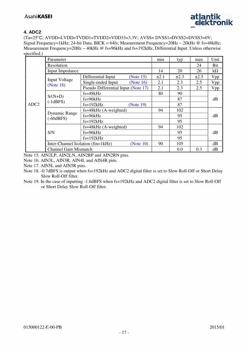
4. ADC2
(Ta=25C; AVDD=LVDD=TVDD1=TVDD2=VDD33=3.3V; AVSS= DVSS1=DVSS2=DVSS3=0V;
Signal Frequency=1kHz; 24-bit Data, BICK = 64fs; Measurement Frequency=20Hz ~ 20kHz @ fs=48kHz;
Measurement Frequency=20Hz ~ 40kHz @ fs=96kHz and fs=192kHz, Differential Input, Unless otherwise
specified.)
Note 15. AIN2LP, AIN2LN, AIN2RP and AIN2RN pins.
Note 16. AIN3L, AIN3R, AIN4L and AIN4R pins.
Note 17. AIN5L and AIN5R pins.
Note 18. -0.7dBFS is output when fs=192kHz and ADC2 digital filter is set to Slow Roll-Off or Short Delay
Slow Roll-Off filter.
Note 19. In the case of inputting -1.6dBFS when fs=192kHz and ADC2 digital filter is set to Slow Roll-Off
or Short Delay Slow Roll-Off filter.
ADC2
Parameter min typ max Unit
Resolution 24 Bit
Input Impedance 14 20 26 kΩ
Input Voltage
(Note 18)
Differential Input (Note 15) ±2.1 ±2.3 ±2.5 Vpp
Single-ended Input (Note 16) 2.1 2.3 2.5 Vpp
Pseudo Differential Input (Note 17) 2.1 2.3 2.5 Vpp
S/(N+D)
(-1dBFS)
fs=48kHz 80 90
dB fs=96kHz 87
fs=192kHz (Note 19) 87
Dynamic Range
(-60dBFS)
fs=48kHz (A-weighted) 94 102
dB fs=96kHz 95
fs=192kHz 95
S/N
fs=48kHz (A-weighted) 94 102
dB fs=96kHz 95
fs=192kHz 95
Inter-Channel Isolation (fin=1kHz) (Note 10) 90 105 dB
Channel Gain Mismatch 0.0 0.3 dB
[AK7738]
015000122-E-00-PB 2015/01
- 18 -
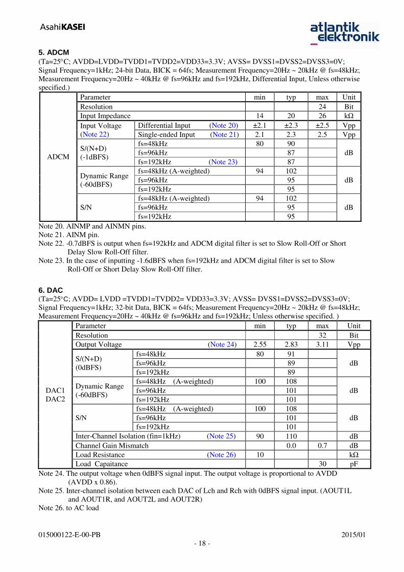
5. ADCM
(Ta=25C; AVDD=LVDD=TVDD1=TVDD2=VDD33=3.3V; AVSS= DVSS1=DVSS2=DVSS3=0V;
Signal Frequency=1kHz; 24-bit Data, BICK = 64fs; Measurement Frequency=20Hz ~ 20kHz @ fs=48kHz;
Measurement Frequency=20Hz ~ 40kHz @ fs=96kHz and fs=192kHz, Differential Input, Unless otherwise
specified.)
Note 20. AINMP and AINMN pins.
Note 21. AINM pin.
Note 22. -0.7dBFS is output when fs=192kHz and ADCM digital filter is set to Slow Roll-Off or Short
Delay Slow Roll-Off filter.
Note 23. In the case of inputting -1.6dBFS when fs=192kHz and ADCM digital filter is set to Slow
Roll-Off or Short Delay Slow Roll-Off filter.
6. DAC (Ta=25C; AVDD= LVDD =TVDD1=TVDD2= VDD33=3.3V; AVSS= DVSS1=DVSS2=DVSS3=0V;
Signal Frequency=1kHz; 32-bit Data, BICK = 64fs; Measurement Frequency=20Hz ~ 20kHz @ fs=48kHz;
Measurement Frequency=20Hz ~ 40kHz @ fs=96kHz and fs=192kHz; Unless otherwise specified. )
DAC1
DAC2
Parameter min typ max Unit
Resolution 32 Bit
Output Voltage (Note 24) 2.55 2.83 3.11 Vpp
S/(N+D)
(0dBFS)
fs=48kHz 80 91
dB fs=96kHz 89
fs=192kHz 89
Dynamic Range
(-60dBFS)
fs=48kHz (A-weighted) 100 108
dB fs=96kHz 101
fs=192kHz 101
S/N
fs=48kHz (A-weighted) 100 108
dB fs=96kHz 101
fs=192kHz 101
Inter-Channel Isolation (fin=1kHz) (Note 25) 90 110 dB
Channel Gain Mismatch 0.0 0.7 dB
Load Resistance (Note 26) 10 kΩ
Load Capaitance 30 pF
Note 24. The output voltage when 0dBFS signal input. The output voltage is proportional to AVDD
(AVDD x 0.86).
Note 25. Inter-channel isolation between each DAC of Lch and Rch with 0dBFS signal input. (AOUT1L
and AOUT1R, and AOUT2L and AOUT2R)
Note 26. to AC load
ADCM
Parameter min typ max Unit
Resolution 24 Bit
Input Impedance 14 20 26 kΩ
Input Voltage
(Note 22)
Differential Input (Note 20) ±2.1 ±2.3 ±2.5 Vpp
Single-ended Input (Note 21) 2.1 2.3 2.5 Vpp
S/(N+D)
(-1dBFS)
fs=48kHz 80 90
dB fs=96kHz 87
fs=192kHz (Note 23) 87
Dynamic Range
(-60dBFS)
fs=48kHz (A-weighted) 94 102
dB fs=96kHz 95
fs=192kHz 95
S/N
fs=48kHz (A-weighted) 94 102
dB fs=96kHz 95
fs=192kHz 95
[AK7738]
015000122-E-00-PB 2015/01
- 19 -
7. SRC (Ta=25C; AVDD=LVDD=TVDD1=TVDD2=VDD33=3.3V; AVSS= DVSS1=DVSS2=DVSS3=0V;
Signal Frequency=1kHz; 24-bit Data; Measurement Frequency=20Hz ~ FSO/2)
SRC
Parameter Symbol min typ max Unit
Resolution 24 Bit
Input Sample Rate FSI 8 192
(Note 27)
kHz
Output Sample Rate FSO 8 192 kHz
THD+N (Input=1kHz, 0dBFS)
FSO/FSI=192kHz/48kHz
FSO/FSI=192kHz/44.1kHz
FSO/FSI=44.1kHz/48kHz
FSO/FSI=44.1kHz/96kHz
FSO/FSI=48kHz/44.1kHz
FSO/FSI=48kHz/96kHz
FSO/FSI=48kHz/8kHz
FSO/FSI=16kHz/48kHz
FSO/FSI=16kHz/44.1kHz
FSO/FSI=8kHz/48kHz
FSO/FSI=8kHz/44.1kHz
FSO/FSI=48kHz/192kHz
FSO/FSI=44.1kHz/192kHz
-113
-113
-112
-111
-112
-113
-111
-113
-100
-113
-95
-105
-102
-103
dB
dB
dB
dB
dB
dB
dB
dB
dB
dB
dB
dB
dB
Dynamic Range (Input=1kHz, -60dBFS)
FSO/FSI=192kHz/48kHz
FSO/FSI=192kHz/44.1kHz
FSO/FSI=44.1kHz/48kHz
FSO/FSI=44.1kHz/96kHz
FSO/FSI=48kHz/44.1kHz
FSO/FSI=48kHz/96kHz
FSO/FSI=48kHz/8kHz
FSO/FSI=16kHz/48kHz
FSO/FSI=16kHz/44.1kHz
FSO/FSI=8kHz/48kHz
FSO/FSI=8kHz/44.1kHz
FSO/FSI=48kHz/192kHz
FSO/FSI=44.1kHz/192kHz
108
113
113
113
113
113
113
113
113
113
111
114
111
110
dB
dB
dB
dB
dB
dB
dB
dB
dB
dB
dB
dB
dB
Dynamic Range
(Input=1kHz, -60dBFS, A-weighted)
FSO/FSI=44.1kHz/48kHz
115
dB
Ratio between Input and Output Sample Rate FSO/FSI 0.167 6 -
Note 27. Set FSI frequency of each operating SRC as the sum of the frequencies is below 384kHz. For
example, if the frequency of FSI is 96kHz, four SRCs can operate at the same time, if the
frequency of FSI is 192kHz, only two SRCs are allowed to operate at the same time.
[AK7738]
015000122-E-00-PB 2015/01
- 20 -
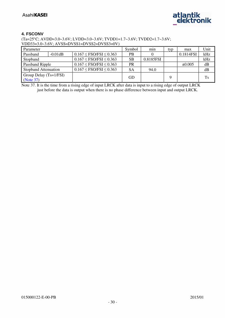
8. FSCONV
(Ta=25C; AVDD=LVDD=TVDD1=TVDD2=VDD33=3.3V; AVSS= DVSS1=DVSS2=DVSS3=0V;
Signal Frequency=1kHz; 24-bit Data; Measurement Frequency=20Hz ~ FSO/2)
FSCONV
Parameter Symbol min typ max Unit
Resolution 24 Bit
Input Sample Rate FSI 44.1 48 kHz
Output Sample Rate FSO 8 16 kHz
THD+N (Input=1kHz, 0dBFS)
FSO/FSI=16kHz/48kHz
FSO/FSI=16kHz/44.1kHz
FSO/FSI=8kHz/48kHz
FSO/FSI=8kHz/44.1kHz
-114
-95
-115
-97
dB
dB
dB
dB
Dynamic Range (Input=1kHz, -60dBFS)
FSO/FSI=16kHz/48kHz
FSO/FSI=16kHz/44.1kHz
FSO/FSI=8kHz/48kHz
FSO/FSI=8kHz/44.1kHz
114
114
114
114
dB
dB
dB
dB
Dynamic Range
(Input=1kHz, -60dBFS, A-weighted)
FSO/FSI=8kHz/48kHz
117
dB
Ratio between Input and Output Sample Rate FSO/FSI 0.167 0.363 -
■ Power Consumption (Ta=25C; AVDD=3.0~3.6V(typ=3.3V, max=3.6V); LVDD=3.0~3.6V(typ=3.3V, max=3.6V);
TVDD1=1.7~3.6V(typ=3.3V, max=3.6V); TVDD2=1.7~3.6V (typ=3.3V, max=3.6V); VDD33=3.0~3.6V
(typ=3.3V, max=3.6V); AVSS= DVSS1=DVSS2=DVSS3=0V; fs=192kHz; BICK=64fs;
SDOUT1~6/LRCK1~5/BICK1~5=Output; CL=20pF)
Parameter Symbol min typ max Unit
Power-Up (PDN pin= “H”)
(Note 28)
AVDD 26 37 mA
LVDD 70 140 mA
TVDD1 1.6 2.4 mA
TVDD2 1.6 2.4 mA
VDD33 4 6 mA
Power-Down (PDN pin= “L”)
AVDD 0.01 mA
LVDD 0.01 mA
TVDD1 0.01 mA
TVDD2 0.01 mA
VDD33 0.01 mA
Note 28. The current of LVDD changes depending on the system frequency and contents of DSP program.
[AK7738]
015000122-E-00-PB 2015/01
- 21 -
9. Digital Filter Characteristics
1. ADC Block
(Ta=25C; AVDD=3.0~3.6V; LVDD=3.0~3.6V; TVDD1=1.7~3.6V; TVDD2=1.7~3.6V;
VDD33=3.0~3.6V; AVSS=DVSS1=DVSS2=DVSS3=0V)
1-1 Sharp Roll-Off Filter (ADSD bit = “0”, ADSL bit = “0”)
fs=48kHz
Parameter Symbol min typ max Unit
SHARP ROLL-OFF
Passband (Note 29) 0dB ~ -0.06dB PB 0 22.1 kHz
-6.0dB PB 24.4 kHz Stopband (Note 29) SB 27.8 kHz
Stopband Attenuation SA 85 dB Group Delay Distortion : 0Hz~20kHz GD 0 1/fs Group Delay (Note 30) GD 19 1/fs
ADC Digital Filter(HPF)
Frequency Response -3.0dB FR 1.0 Hz
fs=96kHz
Parameter Symbol min typ max Unit
SHARP ROLL-OFF
Passband (Note 29) 0dB ~ -0.06dB PB 0 44.2 kHz -6.0dB PB 48.7 kHz
Stopband (Note 29) SB 55.6 kHz Stopband Attenuation SA 85 dB Group Delay Distortion : 0Hz~40kHz GD 0 1/fs
Group Delay (Note 30) GD 19 1/fs
ADC Digital Filter(HPF)
Frequency Response -3.0dB FR 1.9 Hz
fs=192kHz
Parameter Symbol min typ max Unit
SHARP ROLL-OFF
Passband (Note 29) 0dB ~ -0.04dB PB 0 83.7 kHz
-6.0dB PB 100.1 kHz Stopband (Note 29) SB 122.9 kHz
Stopband Attenuation SA 85 dB Group Delay Distortion : 0Hz~40kHz GD 0 1/fs Group Delay (Note 30) GD 15 1/fs
ADC Digital Filter(HPF)
Frequency Response -3.0dB FR 3.9 Hz
[AK7738]
015000122-E-00-PB 2015/01
- 22 -
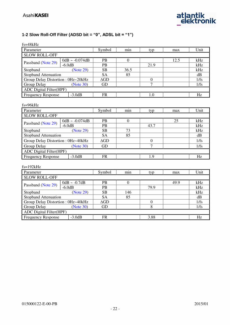
1-2 Slow Roll-Off Filter (ADSD bit = “0”, ADSL bit = “1”)
fs=48kHz
Parameter Symbol min typ max Unit
SLOW ROLL-OFF
Passband (Note 29) 0dB ~ -0.074dB PB 0 12.5 kHz -6.0dB PB 21.9 kHz
Stopband (Note 29) SB 36.5 kHz
Stopband Attenuation SA 85 dB Group Delay Distortion : 0Hz~20kHz GD 0 1/fs Group Delay (Note 30) GD 7 1/fs
ADC Digital Filter(HPF)
Frequency Response -3.0dB FR 1.0 Hz
fs=96kHz
Parameter Symbol min typ max Unit
SLOW ROLL-OFF
Passband (Note 29) 0dB ~ -0.074dB PB 0 25 kHz -6.0dB PB 43.7 kHz
Stopband (Note 29) SB 73 kHz Stopband Attenuation SA 85 dB
Group Delay Distortion : 0Hz~40kHz GD 0 1/fs
Group Delay (Note 30) GD 7 1/fs
ADC Digital Filter(HPF)
Frequency Response -3.0dB FR 1.9 Hz
fs=192kHz
Parameter Symbol min typ max Unit
SLOW ROLL-OFF
Passband (Note 29) 0dB ~ -0.7dB PB 0 49.9 kHz -6.0dB PB 79.9 kHz
Stopband (Note 29) SB 146 kHz Stopband Attenuation SA 85 dB Group Delay Distortion : 0Hz~40kHz GD 0 1/fs Group Delay (Note 30) GD 8 1/fs
ADC Digital Filter(HPF)
Frequency Response -3.0dB FR 3.88 Hz
[AK7738]
015000122-E-00-PB 2015/01
- 23 -
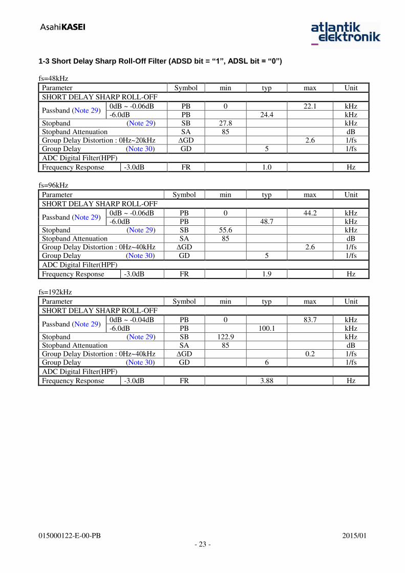
1-3 Short Delay Sharp Roll-Off Filter (ADSD bit = “1”, ADSL bit = “0”)
fs=48kHz
Parameter Symbol min typ max Unit
SHORT DELAY SHARP ROLL-OFF
Passband (Note 29) 0dB ~ -0.06dB PB 0 22.1 kHz -6.0dB PB 24.4 kHz
Stopband (Note 29) SB 27.8 kHz
Stopband Attenuation SA 85 dB Group Delay Distortion : 0Hz~20kHz GD 2.6 1/fs Group Delay (Note 30) GD 5 1/fs
ADC Digital Filter(HPF)
Frequency Response -3.0dB FR 1.0 Hz
fs=96kHz
Parameter Symbol min typ max Unit
SHORT DELAY SHARP ROLL-OFF
Passband (Note 29) 0dB ~ -0.06dB PB 0 44.2 kHz -6.0dB PB 48.7 kHz
Stopband (Note 29) SB 55.6 kHz Stopband Attenuation SA 85 dB Group Delay Distortion : 0Hz~40kHz GD 2.6 1/fs
Group Delay (Note 30) GD 5 1/fs
ADC Digital Filter(HPF)
Frequency Response -3.0dB FR 1.9 Hz
fs=192kHz
Parameter Symbol min typ max Unit
SHORT DELAY SHARP ROLL-OFF
Passband (Note 29) 0dB ~ -0.04dB PB 0 83.7 kHz
-6.0dB PB 100.1 kHz Stopband (Note 29) SB 122.9 kHz Stopband Attenuation SA 85 dB Group Delay Distortion : 0Hz~40kHz GD 0.2 1/fs Group Delay (Note 30) GD 6 1/fs
ADC Digital Filter(HPF)
Frequency Response -3.0dB FR 3.88 Hz
[AK7738]
015000122-E-00-PB 2015/01
- 24 -
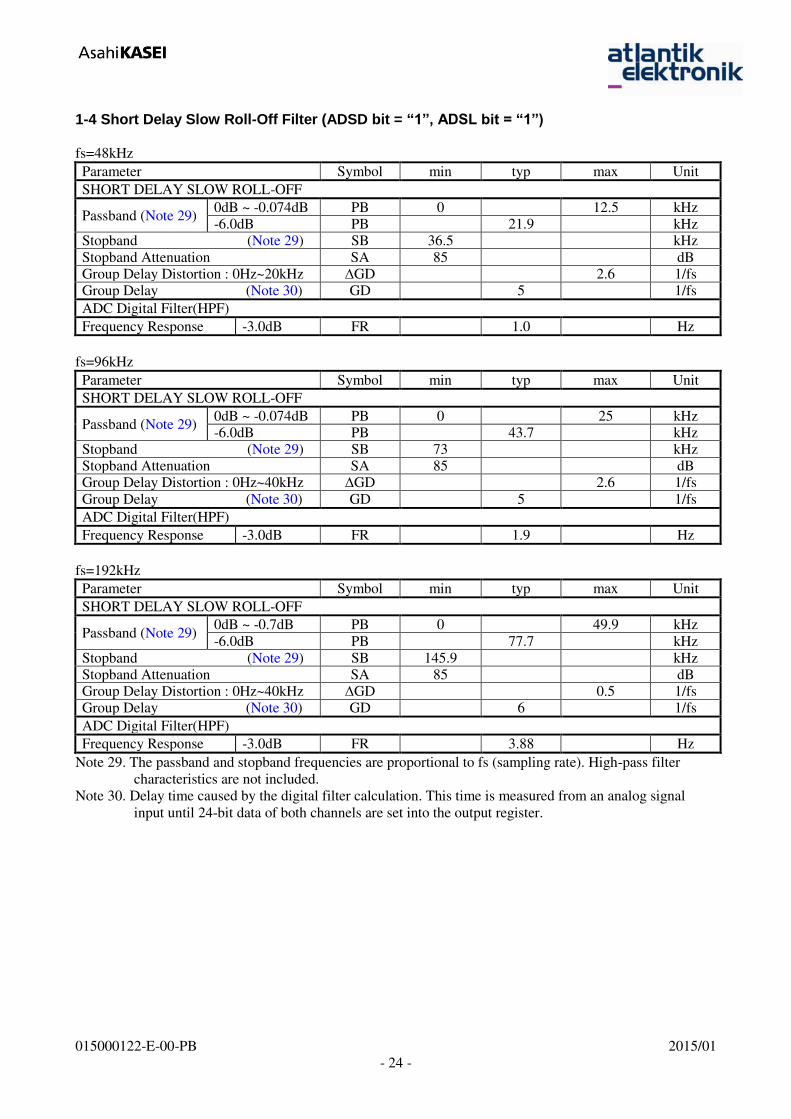
1-4 Short Delay Slow Roll-Off Filter (ADSD bit = “1”, ADSL bit = “1”)
fs=48kHz
Parameter Symbol min typ max Unit
SHORT DELAY SLOW ROLL-OFF
Passband (Note 29) 0dB ~ -0.074dB PB 0 12.5 kHz -6.0dB PB 21.9 kHz
Stopband (Note 29) SB 36.5 kHz
Stopband Attenuation SA 85 dB Group Delay Distortion : 0Hz~20kHz GD 2.6 1/fs Group Delay (Note 30) GD 5 1/fs
ADC Digital Filter(HPF)
Frequency Response -3.0dB FR 1.0 Hz
fs=96kHz
Parameter Symbol min typ max Unit
SHORT DELAY SLOW ROLL-OFF
Passband (Note 29) 0dB ~ -0.074dB PB 0 25 kHz -6.0dB PB 43.7 kHz
Stopband (Note 29) SB 73 kHz Stopband Attenuation SA 85 dB Group Delay Distortion : 0Hz~40kHz GD 2.6 1/fs
Group Delay (Note 30) GD 5 1/fs
ADC Digital Filter(HPF)
Frequency Response -3.0dB FR 1.9 Hz
fs=192kHz
Parameter Symbol min typ max Unit
SHORT DELAY SLOW ROLL-OFF
Passband (Note 29) 0dB ~ -0.7dB PB 0 49.9 kHz
-6.0dB PB 77.7 kHz
Stopband (Note 29) SB 145.9 kHz Stopband Attenuation SA 85 dB Group Delay Distortion : 0Hz~40kHz GD 0.5 1/fs Group Delay (Note 30) GD 6 1/fs
ADC Digital Filter(HPF)
Frequency Response -3.0dB FR 3.88 Hz
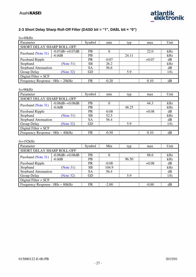
Note 29. The passband and stopband frequencies are proportional to fs (sampling rate). High-pass filter
characteristics are not included.
Note 30. Delay time caused by the digital filter calculation. This time is measured from an analog signal
input until 24-bit data of both channels are set into the output register.
[AK7738]
015000122-E-00-PB 2015/01
- 25 -
2. DAC Block
(Ta= 25C; AVDD=3.0~3.6V; LVDD=3.0~3.6V; TVDD1=1.7~3.6V; TVDD2=1.7~3.6V;
VDD33=3.0~3.6V; AVSS=DVSS1=DVSS2=DVSS3=0V)
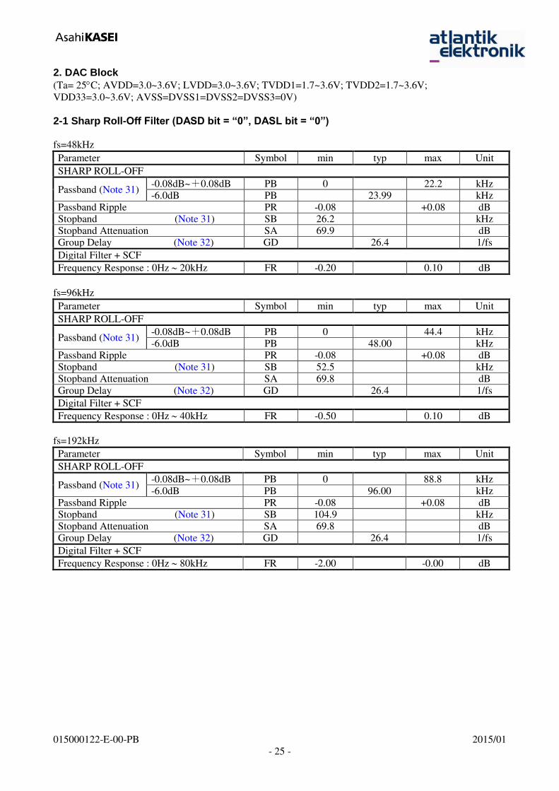
2-1 Sharp Roll-Off Filter (DASD bit = “0”, DASL bit = “0”) fs=48kHz
Parameter Symbol min typ max Unit
SHARP ROLL-OFF
Passband (Note 31) -0.08dB~+0.08dB PB 0 22.2 kHz -6.0dB PB 23.99 kHz
Passband Ripple PR -0.08 +0.08 dB Stopband (Note 31) SB 26.2 kHz
Stopband Attenuation SA 69.9 dB Group Delay (Note 32) GD 26.4 1/fs
Digital Filter + SCF
Frequency Response : 0Hz 20kHz FR -0.20 0.10 dB
fs=96kHz
Parameter Symbol min typ max Unit
SHARP ROLL-OFF
Passband (Note 31) -0.08dB~+0.08dB PB 0 44.4 kHz -6.0dB PB 48.00 kHz
Passband Ripple PR -0.08 +0.08 dB Stopband (Note 31) SB 52.5 kHz Stopband Attenuation SA 69.8 dB
Group Delay (Note 32) GD 26.4 1/fs
Digital Filter + SCF
Frequency Response : 0Hz 40kHz FR -0.50 0.10 dB
fs=192kHz
Parameter Symbol min typ max Unit
SHARP ROLL-OFF
Passband (Note 31) -0.08dB~+0.08dB PB 0 88.8 kHz
-6.0dB PB 96.00 kHz Passband Ripple PR -0.08 +0.08 dB Stopband (Note 31) SB 104.9 kHz Stopband Attenuation SA 69.8 dB Group Delay (Note 32) GD 26.4 1/fs
Digital Filter + SCF
Frequency Response : 0Hz 80kHz FR -2.00 -0.00 dB
[AK7738]
015000122-E-00-PB 2015/01
- 26 -
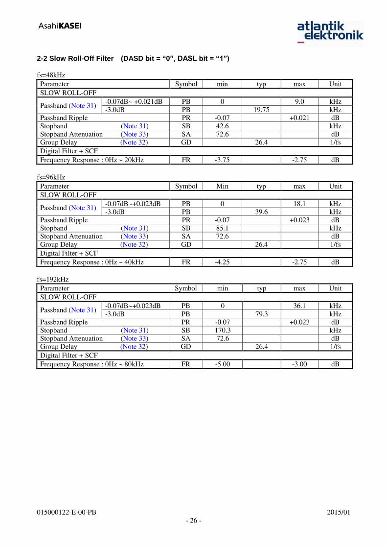
2-2 Slow Roll-Off Filter (DASD bit = “0”, DASL bit = “1”)
fs=48kHz
Parameter Symbol min typ max Unit
SLOW ROLL-OFF
Passband (Note 31) -0.07dB~ +0.021dB PB 0 9.0 kHz -3.0dB PB 19.75 kHz
Passband Ripple PR -0.07 +0.021 dB
Stopband (Note 31) SB 42.6 kHz Stopband Attenuation (Note 33) SA 72.6 dB Group Delay (Note 32) GD 26.4 1/fs
Digital Filter + SCF
Frequency Response : 0Hz 20kHz FR -3.75 -2.75 dB
fs=96kHz
Parameter Symbol Min typ max Unit
SLOW ROLL-OFF
Passband (Note 31) -0.07dB~+0.023dB PB 0 18.1 kHz -3.0dB PB 39.6 kHz
Passband Ripple PR -0.07 +0.023 dB Stopband (Note 31) SB 85.1 kHz Stopband Attenuation (Note 33) SA 72.6 dB
Group Delay (Note 32) GD 26.4 1/fs
Digital Filter + SCF
Frequency Response : 0Hz 40kHz FR -4.25 -2.75 dB
fs=192kHz
Parameter Symbol min typ max Unit
SLOW ROLL-OFF
Passband (Note 31) -0.07dB~+0.023dB PB 0 36.1 kHz
-3.0dB PB 79.3 kHz Passband Ripple PR -0.07 +0.023 dB Stopband (Note 31) SB 170.3 kHz Stopband Attenuation (Note 33) SA 72.6 dB Group Delay (Note 32) GD 26.4 1/fs
Digital Filter + SCF
Frequency Response : 0Hz 80kHz FR -5.00 -3.00 dB
[AK7738]
015000122-E-00-PB 2015/01
- 27 -
2-3 Short Delay Sharp Roll-Off Filter (DASD bit = “1”, DASL bit = “0”)
fs=48kHz
Parameter Symbol min typ max Unit
SHORT DELAY SHARP ROLL-OFF
Passband (Note 31) -0.07dB~+0.07dB PB 0 22.0 kHz -6.0dB PB 24.11 kHz
Passband Ripple PR -0.07 +0.07 dB
Stopband (Note 31) SB 26.2 kHz Stopband Attenuation SA 56.6 dB Group Delay (Note 32) GD 5.9 1/fs
Digital Filter + SCF
Frequency Response : 0Hz 20kHz FR -0.20 0.10 dB
fs=96kHz
Parameter Symbol min typ max Unit
SHORT DELAY SHARP ROLL-OFF
Passband (Note 31) -0.08dB~+0.08dB PB 0 44.3 kHz -6.0dB PB 48.25 kHz
Passband Ripple PR -0.08 +0.08 dB Stopband (Note 31) SB 52.5 kHz Stopband Attenuation SA 56.4 dB Group Delay (Note 32) GD 5.9 1/fs
Digital Filter + SCF
Frequency Response : 0Hz 40kHz FR -0.50 0.10 dB
fs=192kHz
Parameter Symbol Min typ max Unit
SHORT DELAY SHARP ROLL-OFF
Passband (Note 31) -0.08dB~+0.08dB PB 0 88.6 kHz -6.0dB PB 96.50 kHz
Passband Ripple PR -0.08 +0.08 dB Stopband (Note 31) SB 104.9 kHz Stopband Attenuation SA 56.4 dB Group Delay (Note 32) GD 5.9 1/fs
Digital Filter + SCF
Frequency Response : 0Hz 80kHz FR -2.00 -0.00 dB
[AK7738]
015000122-E-00-PB 2015/01
- 28 -
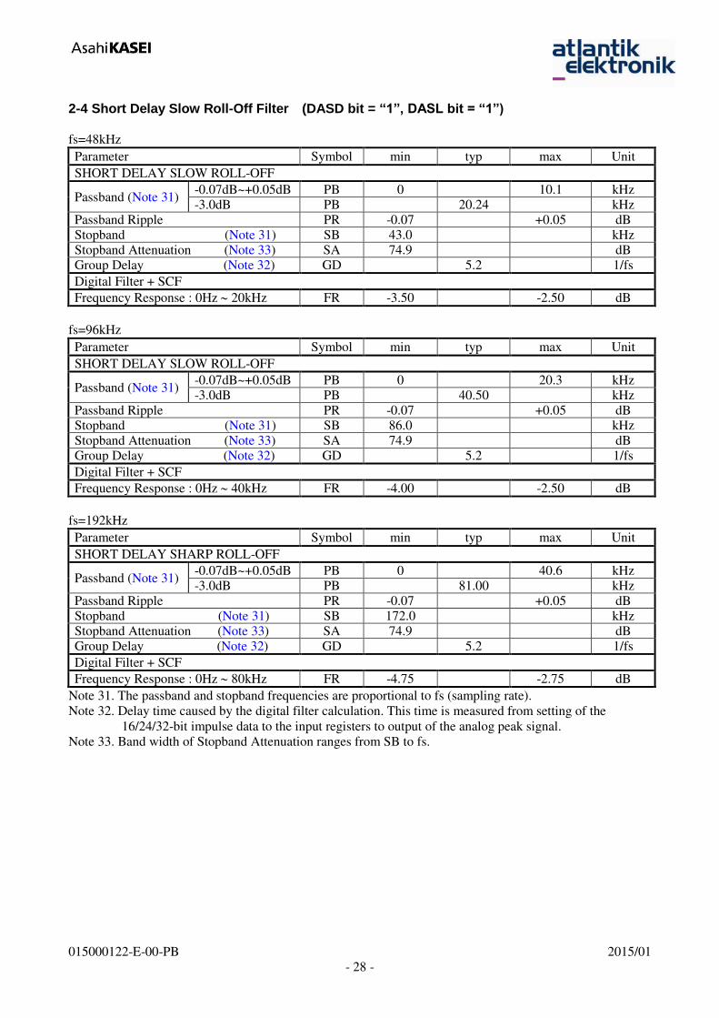
2-4 Short Delay Slow Roll-Off Filter (DASD bit = “1”, DASL bit = “1”)
fs=48kHz
Parameter Symbol min typ max Unit
SHORT DELAY SLOW ROLL-OFF
Passband (Note 31) -0.07dB~+0.05dB PB 0 10.1 kHz -3.0dB PB 20.24 kHz
Passband Ripple PR -0.07 +0.05 dB Stopband (Note 31) SB 43.0 kHz Stopband Attenuation (Note 33) SA 74.9 dB Group Delay (Note 32) GD 5.2 1/fs
Digital Filter + SCF
Frequency Response : 0Hz 20kHz FR -3.50 -2.50 dB
fs=96kHz
Parameter Symbol min typ max Unit
SHORT DELAY SLOW ROLL-OFF
Passband (Note 31) -0.07dB~+0.05dB PB 0 20.3 kHz -3.0dB PB 40.50 kHz
Passband Ripple PR -0.07 +0.05 dB Stopband (Note 31) SB 86.0 kHz Stopband Attenuation (Note 33) SA 74.9 dB Group Delay (Note 32) GD 5.2 1/fs
Digital Filter + SCF
Frequency Response : 0Hz 40kHz FR -4.00 -2.50 dB
fs=192kHz
Parameter Symbol min typ max Unit
SHORT DELAY SHARP ROLL-OFF
Passband (Note 31) -0.07dB~+0.05dB PB 0 40.6 kHz -3.0dB PB 81.00 kHz
Passband Ripple PR -0.07 +0.05 dB Stopband (Note 31) SB 172.0 kHz Stopband Attenuation (Note 33) SA 74.9 dB Group Delay (Note 32) GD 5.2 1/fs
Digital Filter + SCF
Frequency Response : 0Hz 80kHz FR -4.75 -2.75 dB
Note 31. The passband and stopband frequencies are proportional to fs (sampling rate).
Note 32. Delay time caused by the digital filter calculation. This time is measured from setting of the
16/24/32-bit impulse data to the input registers to output of the analog peak signal.
Note 33. Band width of Stopband Attenuation ranges from SB to fs.
[AK7738]
015000122-E-00-PB 2015/01
- 29 -
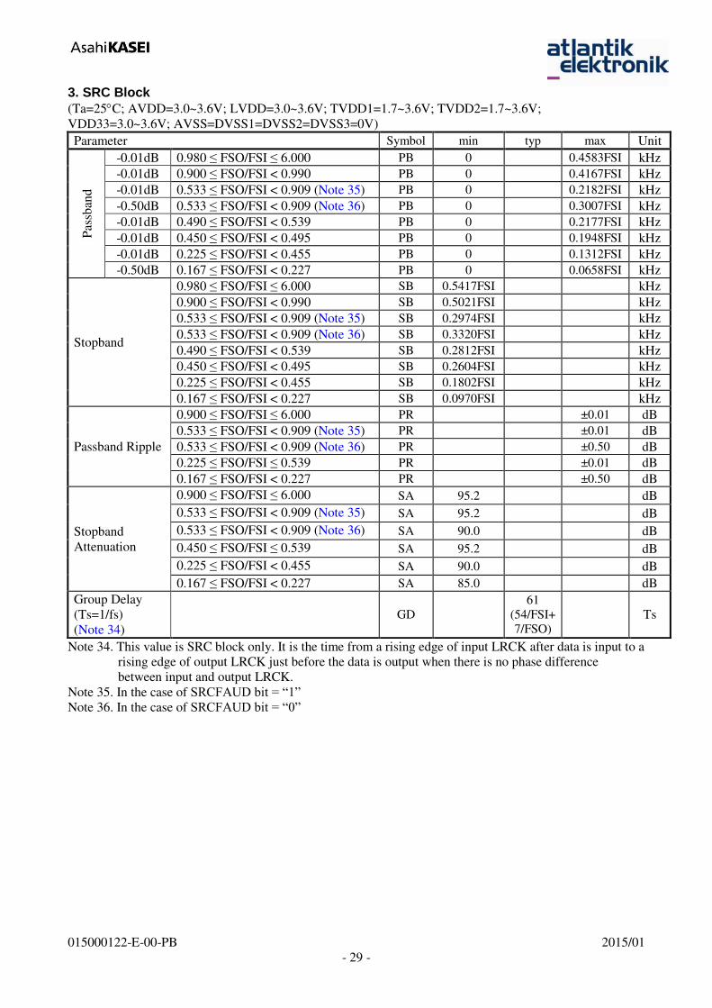
3. SRC Block
(Ta=25C; AVDD=3.0~3.6V; LVDD=3.0~3.6V; TVDD1=1.7~3.6V; TVDD2=1.7~3.6V;
VDD33=3.0~3.6V; AVSS=DVSS1=DVSS2=DVSS3=0V)
Note 34. This value is SRC block only. It is the time from a rising edge of input LRCK after data is input to a
rising edge of output LRCK just before the data is output when there is no phase difference
between input and output LRCK.
Note 35. In the case of SRCFAUD bit = “1”
Note 36. In the case of SRCFAUD bit = “0”
Parameter Symbol min typ max Unit
Pas
sban
d
-0.01dB 0.980 ≤ FSO/FSI ≤ 6.000 PB 0 0.4583FSI kHz
-0.01dB 0.900 ≤ FSO/FSI < 0.990 PB 0 0.4167FSI kHz
-0.01dB 0.533 ≤ FSO/FSI < 0.909 (Note 35) PB 0 0.2182FSI kHz
-0.50dB 0.533 ≤ FSO/FSI < 0.909 (Note 36) PB 0 0.3007FSI kHz
-0.01dB 0.490 ≤ FSO/FSI < 0.539 PB 0 0.2177FSI kHz
-0.01dB 0.450 ≤ FSO/FSI < 0.495 PB 0 0.1948FSI kHz
-0.01dB 0.225 ≤ FSO/FSI < 0.455 PB 0 0.1312FSI kHz
-0.50dB 0.167 ≤ FSO/FSI < 0.227 PB 0 0.0658FSI kHz
Stopband
0.980 ≤ FSO/FSI ≤ 6.000 SB 0.5417FSI kHz
0.900 ≤ FSO/FSI < 0.990 SB 0.5021FSI kHz
0.533 ≤ FSO/FSI < 0.909 (Note 35) SB 0.2974FSI kHz
0.533 ≤ FSO/FSI < 0.909 (Note 36) SB 0.3320FSI kHz
0.490 ≤ FSO/FSI < 0.539 SB 0.2812FSI kHz
0.450 ≤ FSO/FSI < 0.495 SB 0.2604FSI kHz
0.225 ≤ FSO/FSI < 0.455 SB 0.1802FSI kHz
0.167 ≤ FSO/FSI < 0.227 SB 0.0970FSI kHz
Passband Ripple
0.900 ≤ FSO/FSI ≤ 6.000 PR ±0.01 dB
0.533 ≤ FSO/FSI < 0.909 (Note 35) PR ±0.01 dB
0.533 ≤ FSO/FSI < 0.909 (Note 36) PR ±0.50 dB
0.225 ≤ FSO/FSI ≤ 0.539 PR ±0.01 dB
0.167 ≤ FSO/FSI < 0.227 PR ±0.50 dB
Stopband
Attenuation
0.900 ≤ FSO/FSI ≤ 6.000 SA 95.2 dB
0.533 ≤ FSO/FSI < 0.909 (Note 35) SA 95.2 dB
0.533 ≤ FSO/FSI < 0.909 (Note 36) SA 90.0 dB
0.450 ≤ FSO/FSI ≤ 0.539 SA 95.2 dB
0.225 ≤ FSO/FSI < 0.455 SA 90.0 dB
0.167 ≤ FSO/FSI < 0.227 SA 85.0 dB
Group Delay
(Ts=1/fs)
(Note 34)
GD
61
(54/FSI+
7/FSO)
Ts
[AK7738]
015000122-E-00-PB 2015/01
- 30 -
4. FSCONV
(Ta=25C; AVDD=3.0~3.6V; LVDD=3.0~3.6V; TVDD1=1.7~3.6V; TVDD2=1.7~3.6V;
VDD33=3.0~3.6V; AVSS=DVSS1=DVSS2=DVSS3=0V)
Parameter Symbol min typ max Unit
Passband -0.01dB 0.167 ≤ FSO/FSI ≤ 0.363 PB 0 0.1814FSI kHz
Stopband 0.167 ≤ FSO/FSI ≤ 0.363 SB 0.8185FSI kHz
Passband Ripple 0.167 ≤ FSO/FSI ≤ 0.363 PR ±0.005 dB
Stopband Attenuation 0.167 ≤ FSO/FSI ≤ 0.363 SA 94.0 dB
Group Delay (Ts=1/FSI)
(Note 37)
GD 9 Ts
Note 37. It is the time from a rising edge of input LRCK after data is input to a rising edge of output LRCK
just before the data is output when there is no phase difference between input and output LRCK.
[AK7738]
015000122-E-00-PB 2015/01
- 31 -
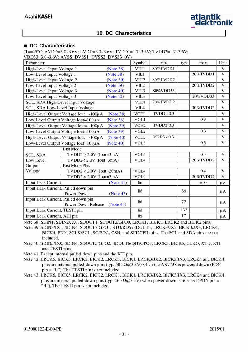
10. DC Characteristics
■ DC Characteristics (Ta=25C; AVDD=3.0~3.6V; LVDD=3.0~3.6V; TVDD1=1.7~3.6V; TVDD2=1.7~3.6V;
VDD33=3.0~3.6V; AVSS=DVSS1=DVSS2=DVSS3=0V)
Parameter Symbol min typ max Unit
High-Level Input Voltage 1 (Note 38) VIH1 80%TVDD1 V
Low-Level Input Voltage 1 (Note 38) VIL1 20%TVDD1 V
High-Level Input Voltage 2 (Note 39) VIH2 80%TVDD2 V
Low-Level Input Voltage 2 (Note 39) VIL2 20%TVDD2 V
High-Level Input Voltage 3 (Note 40) VIH3 80%VDD33 V
Low-Level Input Voltage 3 (Note 40) VIL3 20%VDD33 V
SCL, SDA High-Level Input Voltage VIH4 70%TVDD2 V
SCL, SDA Low-Level Input Voltage VIL4 30%TVDD2 V
High-Level Output Voltage Iout= -100A (Note 38) VOH1 TVDD1-0.3 V
Low-Level Output Voltage Iout=100A (Note 38) VOL1 0.3 V
High-Level Output Voltage Iout= -100A (Note 39) VOH2 TVDD2-0.3 V
Low-Level Output Voltage Iout=100A (Note 39) VOL2 0.3 V
High-Level Output Voltage Iout= -100A (Note 40) VOH3 VDD33-0.3 V
Low-Level Output Voltage Iout=100A (Note 40) VOL3 0.3 V
SCL, SDA
Low Level
Output
Voltage
Fast Mode
TVDD2 ≥ 2.0V (Iout=3mA) VOL4 0.4 V
TVDD2< 2.0V (Iout=3mA) VOL4 20%TVDD2 V
Fast Mode Plus
TVDD2 ≥ 2.0V (Iout=20mA) VOL4 0.4 V
TVDD2 < 2.0V (Iout=3mA) VOL4 20%TVDD2 V
Input Leak Current (Note 41) Iin ±10 A
Input Leak Current, Pulled down pin
Power Down (Note 42) Iid 66 A
Input Leak Current, Pulled down pin
Power Down Release (Note 43) Iid 72 A
Input Leak Current, TESTI pin lid 132 A
Input Leak Current, XTI pin lix 17 A
Note 38. SDIN1, SDIN2/JX0, SDOUT1, SDOUT2/GPO0, LRCK1, BICK1, LRCK2 and BICK2 pins.
Note 39. SDIN3/JX1, SDIN4, SDOUT3/GPO1, STO/RDY/SDOUT4, LRCK3/JX2, BICK3/JX3, LRCK4,
BICK4, PDN, SCLK/SCL, SO/SDA, CSN, and SI/I2CFIL pins. The SCL and SDA pins are not
included.
Note 40. SDIN5/JX0, SDIN6, SDOUT5/GPO2, SDOUT6/DIT/GPO3, LRCK5, BICK5, CLKO, XTO, XTI
and TESTI pins
Note 41. Except internal pulled-down pins and the XTI pin.
Note 42. LRCK5, BICK5, LRCK2, BICK2, LRCK1, BICK1, LRCK3/JX2, BICK3/JX3, LRCK4 and BICK4
pins are internal pulled-down pins (typ. 50 kΩ@3.3↑) when the AK7738 is powered down (PDN
pin = “L”). The TESTI pin is not included.
Note 43. LRCK5, BICK5, LRCK2, BICK2, LRCK1, BICK1, LRCK3/JX2, BICK3/JX3, LRCK4 and BICK4
pins are internal pulled-down pins (typ. 46 kΩ@3.3↑) when power-down is released (PDN pin =
“H”). The TESTI pin is not included.
[AK7738]
015000122-E-00-PB 2015/01
- 32 -
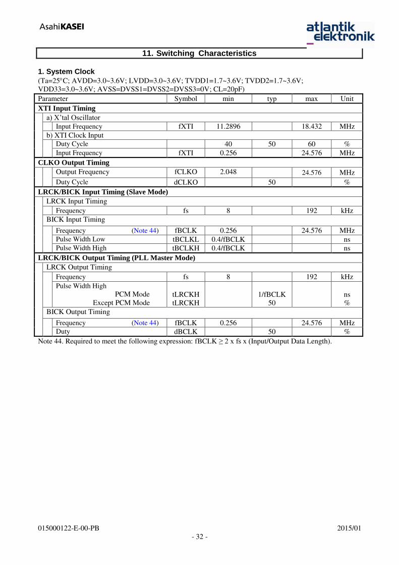
11. Switching Characteristics
1. System Clock
(Ta=25C; AVDD=3.0~3.6V; LVDD=3.0~3.6V; TVDD1=1.7~3.6V; TVDD2=1.7~3.6V;
VDD33=3.0~3.6V; AVSS=DVSS1=DVSS2=DVSS3=0V; CL=20pF)
Parameter Symbol min typ max Unit
XTI Input Timing
a) ↓’tal Oscillator Input Frequency fXTI 11.2896 18.432 MHz
b) XTI Clock Input
Duty Cycle 40 50 60 %
Input Frequency fXTI 0.256 24.576 MHz
CLKO Output Timing
Output Frequency fCLKO 2.048 24.576 MHz
Duty Cycle dCLKO 50 %
LRCK/BICK Input Timing (Slave Mode)
LRCK Input Timing
Frequency fs 8 192 kHz
BICK Input Timing
Frequency (Note 44) fBCLK 0.256 24.576 MHz
Pulse Width Low tBCLKL 0.4/fBCLK ns
Pulse Width High tBCLKH 0.4/fBCLK ns
LRCK/BICK Output Timing (PLL Master Mode)
LRCK Output Timing
Frequency fs 8 192 kHz
Pulse Width High
PCM Mode
Except PCM Mode
tLRCKH
tLRCKH
1/fBCLK
50
ns
%
BICK Output Timing
Frequency (Note 44) fBCLK 0.256 24.576 MHz
Duty dBCLK 50 %
Note 44. Required to meet the following expression: fBCLK ≥ 2 x fs x (Input/Output Data Length).
[AK7738]
015000122-E-00-PB 2015/01
- 33 -
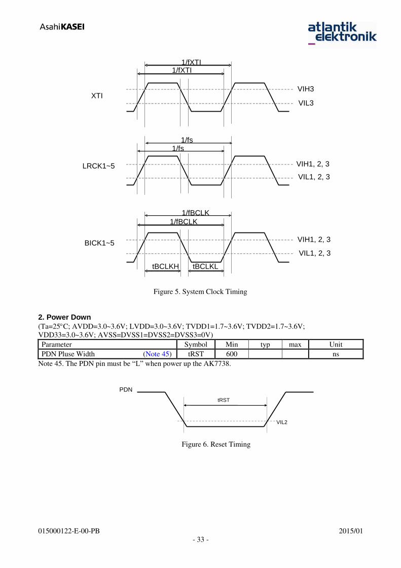
Figure 5. System Clock Timing
2. Power Down
(Ta=25C; AVDD=3.0~3.6V; LVDD=3.0~3.6V; TVDD1=1.7~3.6V; TVDD2=1.7~3.6V;
VDD33=3.0~3.6V; AVSS=DVSS1=DVSS2=DVSS3=0V)
Parameter Symbol Min typ max Unit
PDN Pluse Width (Note 45) tRST 600 ns
Note 45. The PDN pin must be “L” when power up the AK7738.
VIL2
tRST
PDN
Figure 6. Reset Timing
1/fXTI 1/fXTI
VIH3
VIL3 XTI
1/fs
1/fs
tBCLKL tBCLKH
1/fBCLK 1/fBCLK
VIH1, 2, 3
VIL1, 2, 3
LRCK1~5
BICK1~5
VIH1, 2, 3
VIL1, 2, 3
[AK7738]
015000122-E-00-PB 2015/01
- 34 -
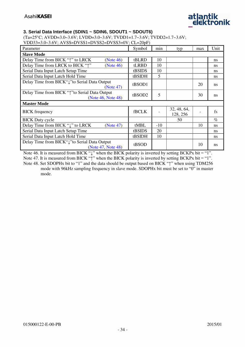
3. Serial Data Interface (SDIN1 ~ SDIN6, SDOUT1 ~ SDOUT6)
(Ta=25C; AVDD=3.0~3.6V; LVDD=3.0~3.6V; TVDD1=1.7~3.6V; TVDD2=1.7~3.6V;
VDD33=3.0~3.6V; AVSS=DVSS1=DVSS2=DVSS3=0V; CL=20pF)
Parameter Symbol min typ max Unit
Slave Mode
Delay Time from BICK “ ” to LRCK (Note 46) tBLRD 10 ns
Delay Time from LRCK to BICK “ ” (Note 46) tLRBD 10 ns
Serial Data Input Latch Setup Time tBSIDS 10 ns
Serial Data Input Latch Hold Time tBSIDH 5 ns
Delay Time from BICK“ ”to Serial Data Output
(Note 47) tBSOD1 20 ns
Delay Time from BICK “ ”to Serial Data Output
(Note 46, Note 48) tBSOD2 5 30 ns
Master Mode
BICK frequency fBCLK - 32, 48, 64,
128, 256 - fs
BICK Duty cycle 50 %
Delay Time from BICK “ ” to LRCK (Note 47) tMBL -10 10 ns
Serial Data Input Latch Setup Time tBSIDS 20 ns
Serial Data Input Latch Hold Time tBSIDH 10 ns
Delay Time from BICK“ ”to Serial Data Output
(Note 47, Note 48) tBSOD 10 ns
Note 46. It is measured from BICK “ ” when the BICK polarity is inverted by setting BCKPx bit = “1”.
Note 47. It is measured from BICK “ ” when the BICK polarity is inverted by setting BCKPx bit = “1”.
Note 48. Set SDOPHx bit to “1” and the data should be output based on BICK “ ” when using TDM256
mode with 96kHz sampling frequency in slave mode. SDOPHx bit must be set to “0” in master
mode.
[AK7738]
015000122-E-00-PB 2015/01
- 35 -
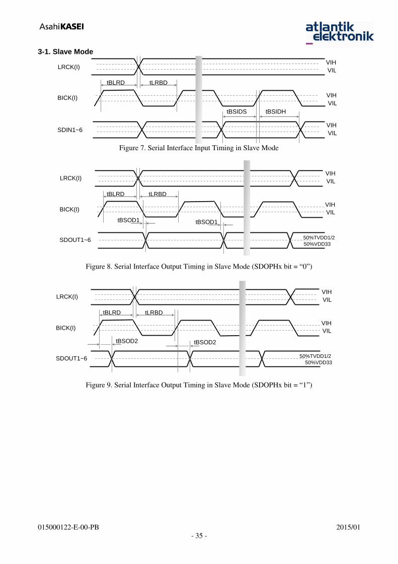
3-1. Slave Mode
tBSIDS
tBLRD tLRBD
VIH
VIL
tBSIDH
SDIN1~6
LRCK(I)
BICK(I) VIH
VIL
VIH
VIL
Figure 7. Serial Interface Input Timing in Slave Mode
VIH
LRCK(I)
BICK(I)
VIL
SDOUT1~6 50%TVDD1/2
tBSOD1
VIH
VIL
50%VDD33
tBLRD tLRBD
tBSOD1
Figure 8. Serial Interface Output Timing in Slave Mode (SDOPHx bit = “0”)
VIH
LRCK(I)
BICK(I)
VIL
SDOUT1~6 50%TVDD1/2
tBSOD2
VIH
VIL
50%VDD33
tBLRD tLRBD
tBSOD2
Figure 9. Serial Interface Output Timing in Slave Mode (SDOPHx bit = “1”)
[AK7738]
015000122-E-00-PB 2015/01
- 36 -
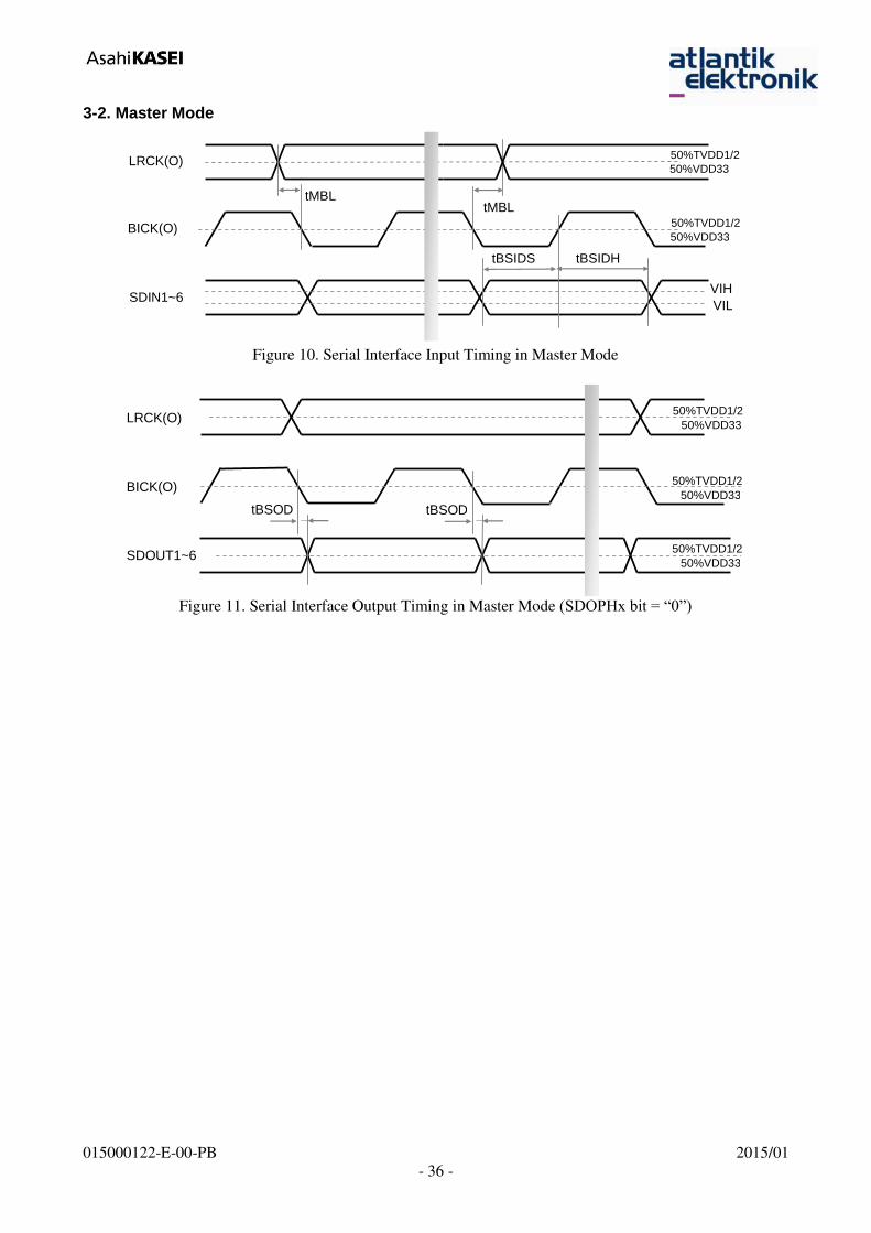
3-2. Master Mode
tBSIDS
tMBL tMBL
LRCK(O)
BICK(O)
VIH
VIL
tBSIDH
SDIN1~6
50%TVDD1/2
50%VDD33
50%TVDD1/2
50%VDD33
Figure 10. Serial Interface Input Timing in Master Mode
tBSOD
LRCK(O)
BICK(O)
SDOUT1~6
50%TVDD1/2
50%VDD33
50%TVDD1/2
50%VDD33
50%TVDD1/2
50%VDD33
tBSOD
Figure 11. Serial Interface Output Timing in Master Mode (SDOPHx bit = “0”)
[AK7738]
015000122-E-00-PB 2015/01
- 37 -
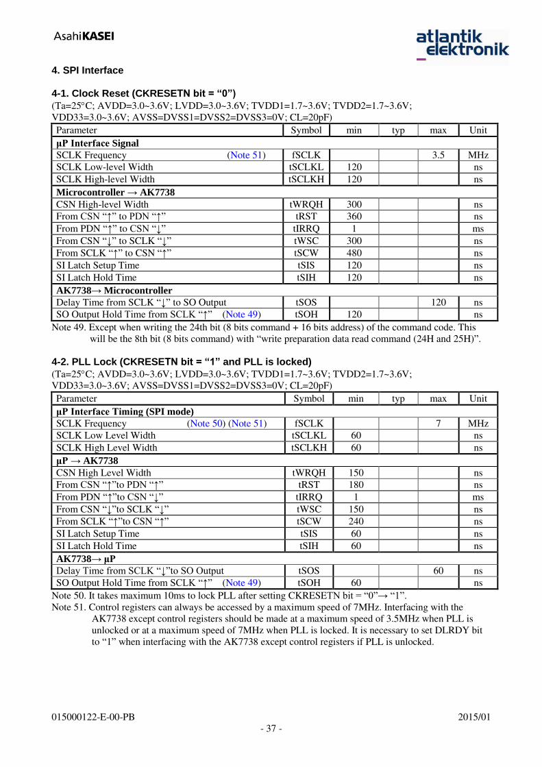
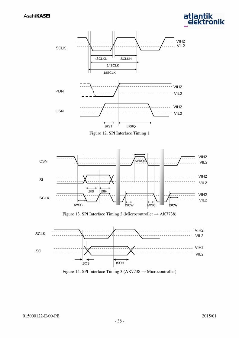
4. SPI Interface
4-1. Clock Reset (CKRESETN bit = “0”)
(Ta=25C; AVDD=3.0~3.6V; LVDD=3.0~3.6V; TVDD1=1.7~3.6V; TVDD2=1.7~3.6V;
VDD33=3.0~3.6V; AVSS=DVSS1=DVSS2=DVSS3=0V; CL=20pF)
Parameter Symbol min typ max Unit
μP Interface Signal
SCLK Frequency (Note 51) fSCLK 3.5 MHz
SCLK Low-level Width tSCLKL 120 ns
SCLK High-level Width tSCLKH 120 ns
Microcontroller → AK7738
CSN High-level Width tWRQH 300 ns
From CSN “ ” to PDN “ ” tRST 360 ns
From PDN “ ” to CSN “ ” tIRRQ 1 ms
From CSN “ ” to SCLK “ ” tWSC 300 ns
From SCLK “ ” to CSN “ ” tSCW 480 ns
SI Latch Setup Time tSIS 120 ns
SI Latch Hold Time tSIH 120 ns
AK7738→ Microcontroller
Delay Time from SCLK “ ” to SO Output tSOS 120 ns
SO Output Hold Time from SCLK “ ” (Note 49) tSOH 120 ns
Note 49. Except when writing the 24th bit (8 bits command + 16 bits address) of the command code. This
will be the 8th bit (8 bits command) with “write preparation data read command (24H and 25H)”.
4-2. PLL Lock (CKRESETN bit = “1” and PLL is locked)
(Ta=25C; AVDD=3.0~3.6V; LVDD=3.0~3.6V; TVDD1=1.7~3.6V; TVDD2=1.7~3.6V;
VDD33=3.0~3.6V; AVSS=DVSS1=DVSS2=DVSS3=0V; CL=20pF)
Parameter Symbol min typ max Unit
μP Interface Timing (SPI mode)
SCLK Frequency (Note 50) (Note 51) fSCLK 7 MHz
SCLK Low Level Width tSCLKL 60 ns
SCLK High Level Width tSCLKH 60 ns
μP → AK7738
CSN High Level Width tWRQH 150 ns
From CSN “ ”to PDN “ ” tRST 180 ns
From PDN “ ”to CSN “ ” tIRRQ 1 ms
From CSN “ ”to SCLK “ ” tWSC 150 ns
From SCLK “ ”to CSN “ ” tSCW 240 ns
SI Latch Setup Time tSIS 60 ns
SI Latch Hold Time tSIH 60 ns
AK7738→ μP
Delay Time from SCLK “ ”to SO Output tSOS 60 ns
SO Output Hold Time from SCLK “ ” (Note 49) tSOH 60 ns
Note 50. It takes maximum 10ms to lock PLL after setting CKRESETN bit = “0” “1”.
Note 51. Control registers can always be accessed by a maximum speed of 7MHz. Interfacing with the
AK7738 except control registers should be made at a maximum speed of 3.5MHz when PLL is
unlocked or at a maximum speed of 7MHz when PLL is locked. It is necessary to set DLRDY bit
to “1” when interfacing with the AK7738 except control registers if PLL is unlocked.
[AK7738]
015000122-E-00-PB 2015/01
- 38 -
tSCLKH
tSCLKL
1/fSCLK
1/fSCLK
SCLK
VIH2 VIL2
VIH2
VIL2
VIH2
VIL2
tRST
PDN
CSN
tIRRQ
Figure 12. SPI Interface Timing 1
tWRQH
tSIS
tSIH
tSCW tSCW tWSC tSCW
CSN
SI VIH2
VIL2
VIH2
tWSC
SCLK VIL2
VIH2
VIL2
Figure 13. SPI Interface Timing 2 (Microcontroller AK7738)
tSOS
tSOH
SCLK VIL2
VIH2
SO VIH2
VIL2
Figure 14. SPI Interface Timing 3 (AK7738 Microcontroller)
[AK7738]
015000122-E-00-PB 2015/01
- 39 -
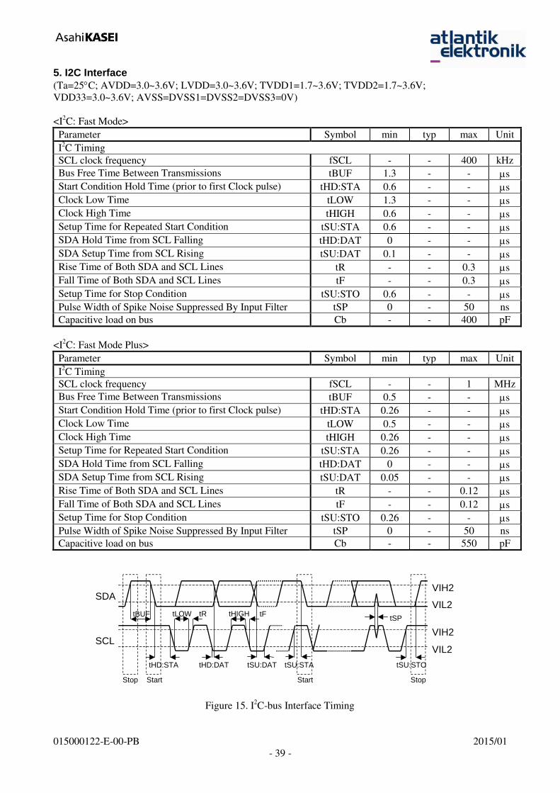
5. I2C Interface
(Ta=25C; AVDD=3.0~3.6V; LVDD=3.0~3.6V; TVDD1=1.7~3.6V; TVDD2=1.7~3.6V;
VDD33=3.0~3.6V; AVSS=DVSS1=DVSS2=DVSS3=0V)
<I2C: Fast Mode>
Parameter Symbol min typ max Unit
I2C Timing
SCL clock frequency fSCL - - 400 kHz
Bus Free Time Between Transmissions tBUF 1.3 - - s
Start Condition Hold Time (prior to first Clock pulse) tHD:STA 0.6 - - s
Clock Low Time tLOW 1.3 - - s
Clock High Time tHIGH 0.6 - - s
Setup Time for Repeated Start Condition tSU:STA 0.6 - - s
SDA Hold Time from SCL Falling tHD:DAT 0 - - s
SDA Setup Time from SCL Rising tSU:DAT 0.1 - - s
Rise Time of Both SDA and SCL Lines tR - - 0.3 s
Fall Time of Both SDA and SCL Lines tF - - 0.3 s
Setup Time for Stop Condition tSU:STO 0.6 - - s
Pulse Width of Spike Noise Suppressed By Input Filter tSP 0 - 50 ns
Capacitive load on bus Cb - - 400 pF
<I2C: Fast Mode Plus>
Parameter Symbol min typ max Unit
I2C Timing
SCL clock frequency fSCL - - 1 MHz
Bus Free Time Between Transmissions tBUF 0.5 - - s
Start Condition Hold Time (prior to first Clock pulse) tHD:STA 0.26 - - s
Clock Low Time tLOW 0.5 - - s
Clock High Time tHIGH 0.26 - - s
Setup Time for Repeated Start Condition tSU:STA 0.26 - - s
SDA Hold Time from SCL Falling tHD:DAT 0 - - s
SDA Setup Time from SCL Rising tSU:DAT 0.05 - - s
Rise Time of Both SDA and SCL Lines tR - - 0.12 s
Fall Time of Both SDA and SCL Lines tF - - 0.12 s
Setup Time for Stop Condition tSU:STO 0.26 - - s
Pulse Width of Spike Noise Suppressed By Input Filter tSP 0 - 50 ns
Capacitive load on bus Cb - - 550 pF
tHIGH
SCL
SDA VIH2
tLOW tBUF
tHD:STA
tR tF
tHD:DAT tSU:DAT tSU:STA
Stop Start Start Stop
tSU:STO
VIL2
VIH2
VIL2
tSP
Figure 15. I2C-bus Interface Timing
[AK7738]
015000122-E-00-PB 2015/01
- 40 -
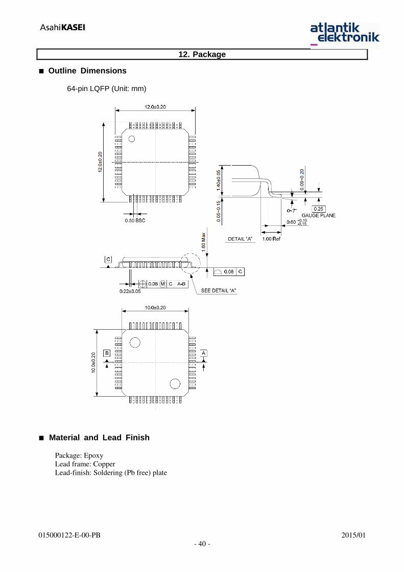
12. Package
■ Outline Dimensions
64-pin LQFP (Unit: mm)
■ Material and Lead Finish
Package: Epoxy
Lead frame: Copper
Lead-finish: Soldering (Pb free) plate
[AK7738]
015000122-E-00-PB 2015/01
- 41 -
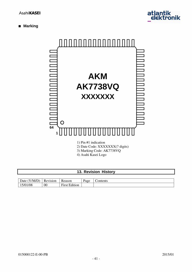
■ Marking
1) Pin #1 indication
2) Date Code: XXXXXXX(7 digits)
3) Marking Code: AK7738VQ
4) Asahi Kasei Logo
13. Revision History
Date (Y/M/D) Revision Reason Page Contents
15/01/08 00 First Edition
AK7738VQ XXXXXXX
AKM
1
64
[AK7738]
015000122-E-00-PB 2015/01
- 42 -
Thank you for your access to AKM product information. More detail product information is available, please contact
our sales office or authorized distributors.
IMPORTANT NOTICE
0. Asahi Kasei Microdevices Corporation (“AKM”) reserves the right to make changes to the information contained in this document without notice. When you consider any use or application of AKM product stipulated in this document (“Product”), please make inquiries the sales office of AKM or authorized distributors as to current status of the Products.
1. All information included in this document are provided only to illustrate the operation and application examples of AKM Products. AKM neither makes warranties or representations with respect to the accuracy or completeness of the information contained in this document nor grants any license to any intellectual property rights or any other rights of AKM or any third party with respect to the information in this document. You are fully responsible for use of such information contained in this document in your product design or applications. AKM ASSUMES NO LIABILITY FOR ANY LOSSES INCURRED BY YOU OR THIRD PARTIES ARISING FROM THE USE OF SUCH INFORMATION IN YOUR PRODUCT DESIGN OR APPLICATIONS.
2. The Product is neither intended nor warranted for use in equipment or systems that require extraordinarily high levels of quality and/or reliability and/or a malfunction or failure of which may cause loss of human life, bodily injury, serious property damage or serious public impact, including but not limited to, equipment used in nuclear facilities, equipment used in the aerospace industry, medical equipment, equipment used for automobiles, trains, ships and other transportation, traffic signaling equipment, equipment used to control combustions or explosions, safety devices, elevators and escalators, devices related to electric power, and equipment used in finance-related fields. Do not use Product for the above use unless specifically agreed by AKM in writing.
3. Though AKM works continually to improve the Product’s quality and reliability, you are responsible for complying with safety standards and for providing adequate designs and safeguards for your hardware, software and systems which minimize risk and avoid situations in which a malfunction or failure of the Product could cause loss of human life, bodily injury or damage to property, including data loss or corruption.
4. Do not use or otherwise make available the Product or related technology or any information contained in this document for any military purposes, including without limitation, for the design, development, use, stockpiling or manufacturing of nuclear, chemical, or biological weapons or missile technology products (mass destruction weapons). When exporting the Products or related technology or any information contained in this document, you should comply with the applicable export control laws and regulations and follow the procedures required by such laws and regulations. The Products and related technology may not be used for or incorporated into any products or systems whose manufacture, use, or sale is prohibited under any applicable domestic or foreign laws or regulations.
5. Please contact AKM sales representative for details as to environmental matters such as the RoHS compatibility of the Product. Please use the Product in compliance with all applicable laws and regulations that regulate the inclusion or use of controlled substances, including without limitation, the EU RoHS Directive. AKM assumes no liability for damages or losses occurring as a result of noncompliance with applicable laws and regulations.
6. Resale of the Product with provisions different from the statement and/or technical features set forth in this document shall immediately void any warranty granted by AKM for the Product and shall not create or extend in any manner whatsoever, any liability of AKM.
7. This document may not be reproduced or duplicated, in any form, in whole or in part, without prior written consent of AKM.


![ISD8102 / ISD8104 - Atlantik Elektronik · The ISD8102/ ISD8104 are a general purpose analog audio amplifier, ... Atlantik Elektronik GmbH ... PARAMETER SYMBOL MIN TYP [1]](https://img.pdfslide.us/doc/110x75/5ca4dd7788c99388188b79ca/isd8102-isd8104-atlantik-the-isd8102-isd8104-are-a-general-purpose-analog.jpg)