Embed Size (px)
DESCRIPTION
AHB
Citation preview

1
ARM® AMBA®3 AHB-Lite*
Karthik Shivashankar
ARM LTD., Cambridge, UK
MIT SoC Design CompetitionONE BOARD, ONE MONTH, UNLIMITED POSSIBILITIES....

2
About Me
Sr. Engineer @ ARM Research
Based in Cambridge, UK
4+ years at ARM
Image Source: Google.com

3
Before we start
Have you worked on AMBA before ?
Image Source: Google.com

4
Why we need Architecture Spec ?

5
Why we need Architecture Spec ?

6
Agenda
AMBA Family (2)
Introduction to AHB-Lite (6)
AHB-Lite System (8)
AHB-Lite Signals – Master & Slave (15)
AHB-Lite Transactions (9)
How to build a simple AHB-Lite Slave (4)
AHB-Lite – Multilayer Design (3)
7
Agenda
AMBA Family (2)
Introduction to AHB-Lite (6)
AHB-Lite System (8)
AHB-Lite Signals – Master & Slave (15)
AHB-Lite Transactions (9)
How to build a simple AHB-Lite Slave (4)
AHB-Lite – Multilayer Design (3)

8
AMBA Family
Image Source: Google.com
AMBA-1
AMBA-2
AHB
AMBA-3
AHB-Lite
AMBA-4
Acronyms
AMBA® Advanced Microcontroller Bus Architectures
AHB® Advanced High-Performance Bus

9
Agenda
AMBA Family (2)
Introduction to AHB-Lite (6)
AHB-Lite System (8)
AHB-Lite Signals – Master & Slave (15)
AHB-Lite Transactions (9)
How to build a simple AHB-Lite Slave (4)
AHB-Lite – Multilayer Design (3)

10
Master-Slave Architecture

11
AHB-Lite
Single Master
Simple slaves
Easier module design/debug
No arbitration issues
Master 0
Slave
#1
Slave
#2
Slave
#3
Slave
#4
Image Source: Walt Disney

12
AHB-Lite transactions
Master
Register Read
Register Write
Burst Read
Burst Write
Slave
Can make Master wait
Can give error response
Image Source: Walt Disney

13
AHB-Lite Features
Single Clock Edge operation
Uni-directional busses
No tri-state signals
Good for synthesis
Pipelined Operation
Image Source:: Walt Disney

14
An Example AMBA AHB-Lite System
ARM
Processor
(CM0-DS)
VGA
AHB-Lite
UART GPIO PS2-KB TIMER 7SEG
MEM
CONTROLLER

15
An Example AMBA AHB-Lite System
ARM
Processor
(CM0-DS)
VGA
AHB-Lite
UART GPIO PS2-KB TIMER 7SEG
MEM
CONTROLLER
UARTVGASwitches
& LEDPS2
7-SEG
Display
PSRAM
(16MB)
FLASH
(16 MB)
XILINX SPARTAN6
DIGILENT NEXYS3
PUSH
Buttons

16
An Example AMBA AHB-Lite System

17
ARM R&D Testchip using CM0-DS

18
Agenda
AMBA Family (2)
Introduction to AHB-Lite (6)
AHB-Lite System (8)
AHB-Lite Signals – Master & Slave (15)
AHB-Lite Transactions (9)
How to build a simple AHB-Lite Slave (4)
AHB-Lite – Multilayer Design (3)

19
Main Components of AHB Lite System
Master
Slaves
Address Decoder
Multiplexor

20
AHB-Lite Master
AHB-Lite
Master
Address and
Control
Write DataRead Data
Global Signals
Transfer
Response

21
AHB-Lite Slave
AHB-Lite
Slave
Transfer
Response
Read DataWrite Data
Address and
Control
Slave Select
Global Signal

22
AHB-Lite Master & Slave
Slave Select
AHB-Lite
Master
Address and Control
Write Data
Read Data
Transfer Response
AHB-Lite
Slave
Global Signals

23
Memory Map Decoder & MUX
AHB-Lite
Master
Address, Control & Wdata
Read Data
Transfer
Response
AHB-Lite
Slave
AHB-Lite
Slave
AHB-Lite
Slave
SEL1
SEL2
SEL3
Memory Map
Decoder
ADDR
MUX
MUX SEL
Transfer Response, Rdata 1
FF
Transfer Response, Rdata 2
Transfer Response, Rdata 2
24
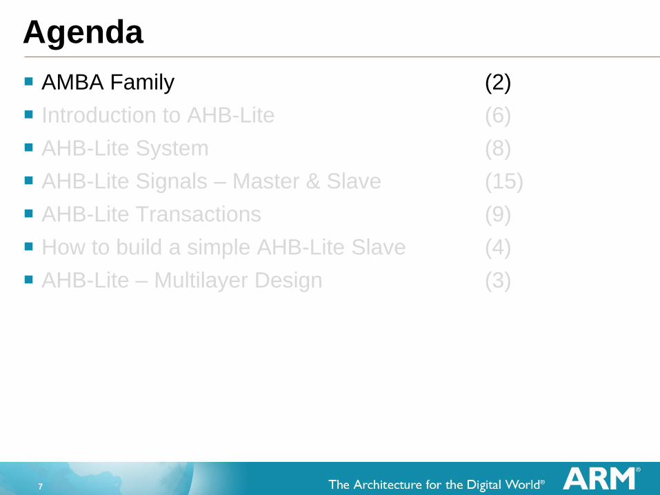
Pipelined Transactions (Conceptual Level)
A
HCLK
Address phaseData phase
N cycles
Address
&
Control
Data
&
Response
A
Memory Mapped Transactions: READ & WRITE

25
Agenda
AMBA Family (2)
Introduction to AHB-Lite (6)
AHB-Lite System (8)
AHB-Lite Signals – Master & Slave (15)
AHB-Lite Transactions (9)
How to build a simple AHB-Lite Slave (4)
AHB-Lite – Multilayer Design (3)

26
AHB-Lite Master Signals
AHB-Lite
Master
Address and
Control
Write DataRead Data
Global Signals
Transfer
Response
27
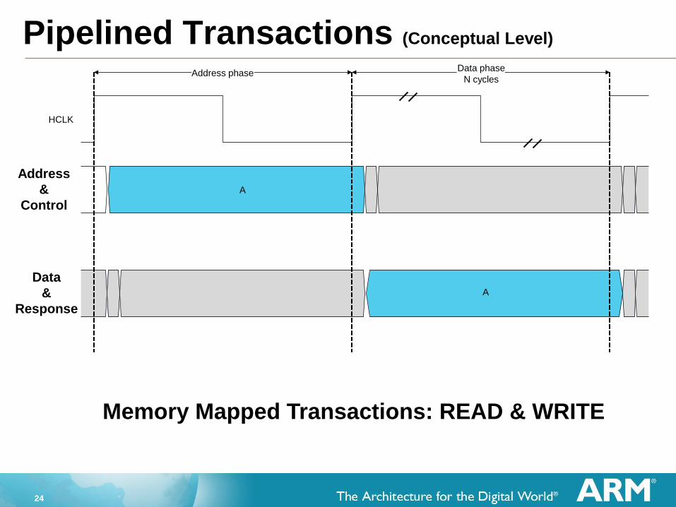
AHB-Lite Slave Signals
AHB-Lite
Slave
Transfer
Response
Read DataWrite Data
Address and
Control
Slave Select
Global Signal

28
AHB-Lite Master & Slave

29
AHB-Lite Master & Slave

30
CM0-DS Doesn’t speak the entire language !
CM0-DS do not generate BURST transaction
HBURST[2:0] is always 3’b000
CM0-DS never generates locked transactions
HMASTLOCK is always 1’b0
All transactions issued are non-sequential transfers
HTRANS[1:0] is either 2’b00 (IDLE) or 2’b10 (Non Sequential)

31
AHB-Lite Master & Slave

32
HSIZE[1:0]

33
HPROT[3:0] Protection Signal Encoding
Master Generates these signals !
Slaves have the freedom to ignore !!
34
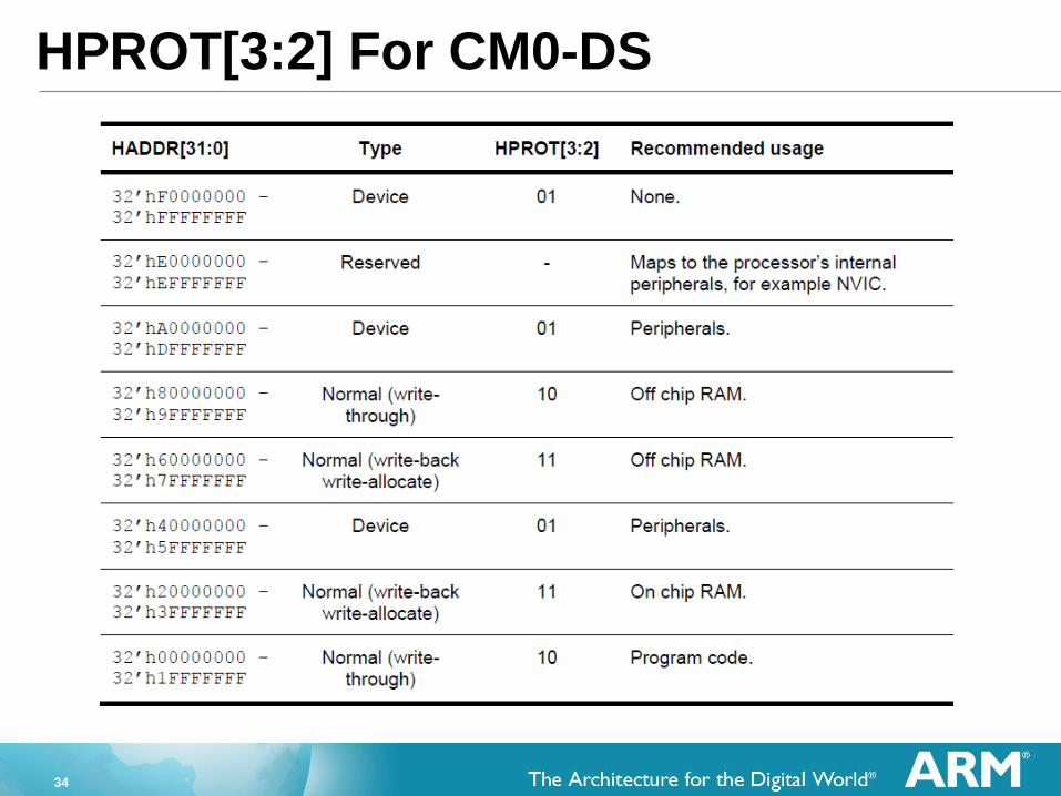
HPROT[3:2] For CM0-DS

35
HTRANS[1:0]
HTRANS Type Description
00 IDLE Master does not wish to perform a transfer
01 BUSY Bus Master is in the middle of a
burst but cannot immediately continue
with the next transfer
10 NON-SEQ Indicates the first transfer of a burst or a
single transfer
11 SEQ The remaining transfers in the burst are
sequential address steps from the previous
transfer. Step size is that of data width of
transfer (which is shown by HSIZE)
CM0-DS Always generates NON-SEQ
Transactions

36
Transactions

37
Control Signals Recap
HTRANS[1:0]
IDLE
BUSY
NONSEQ
SEQ
HBURST[2:0]
SINGLE
INCR
WRAP[4|8|16]
INCR[4|8|16]
HSIZE[2:0]
Byte
Halfword
Word
Doubleword
...
HPROT[3:0]
Data/Opcode
Privileged/user
Bufferable
Cacheable
HMASTLOCK
UNLOCKED
LOCKED

38
Transfer Response Signals

39
AHB-Lite Master & Slave

40
Control Signals to Care about

41
Agenda
AMBA Family (2)
Introduction to AHB-Lite (6)
AHB-Lite System (8)
AHB-Lite Signals – Master & Slave (15)
AHB-Lite Transactions (9)
How to build a simple AHB-Lite Slave (4)
AHB-Lite – Multilayer Design (3)

42
HADDR[31:0] A
HCLK
B
Address phase Data phase
HWRITE
HWDATA[31:0] Data (A)
HREADY
Basic transfer - Write
43
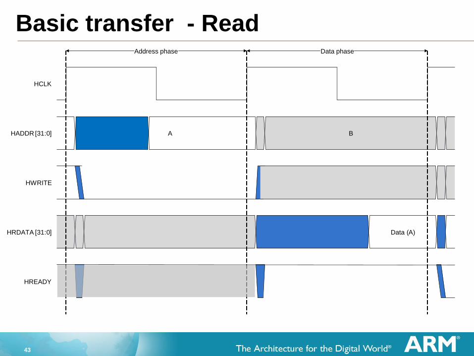
Basic transfer - Read
HRDATA [31:0]
HREADY
HADDR [31:0] A
HCLK
B
Address phase Data phase
HWRITE
Data (A)

44
AHB Pipelined Transaction
HCLK
HADDR
HWRITE
HWDATA
HRDATA
HRESP
HREADY
Address Phase A Data Phase A
Address Phase B
A
A
A
A
Data Phase B
Address Phase C
C
C
B
B
B
B
OKAY A OKAY B
Data Phase C
Address Phase ….
45
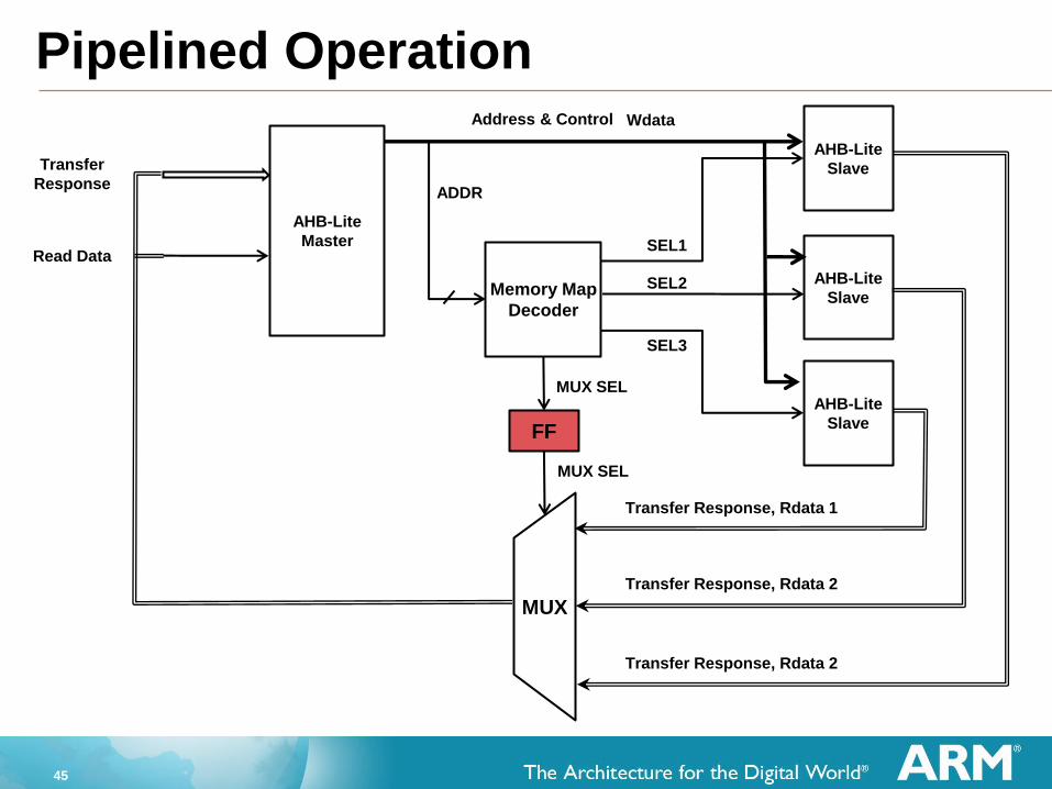
Pipelined Operation
AHB-Lite
MasterRead Data
Transfer
Response
AHB-Lite
Slave
AHB-Lite
Slave
AHB-Lite
Slave
Address & Control
SEL1
SEL2
SEL3
Memory Map
Decoder
ADDR
FF
MUX SEL
Transfer Response, Rdata 1
MUX
MUX SEL
Transfer Response, Rdata 2
Transfer Response, Rdata 2
Wdata

46
AHB basic signal timing – Adding wait states
A
A
A
A
AA
Address Phase
A
Data Phase A
Address Phase B
B
B
OKAY A OKAY A
HCLK
HADDR
HWRITE
HWDATA
HREADY
HRDATA
HRESP
Master will extend Address Phase B

47
HREADY (Inform all)
AHB-Lite
Master
AHB-Lite
Slave 1
AHB-Lite
Slave 2
AHB-Lite
Slave 3
MUX
HREADYOUT 1
HREADYOUT 2
HREADYOUT 3
MUX SEL
FF
HREADY
48
HRESP – Slave Response
HRESP Event Bus Master operation
OKAY Access completed
normally
ERROR Slave aborts access,
(2 cycle response)
Master has option of
continuing or terminating
a burst containing an
ERROR
It is permissible to continuously drive HRESP
Low in a system which does not wish to
generate any errors.
49
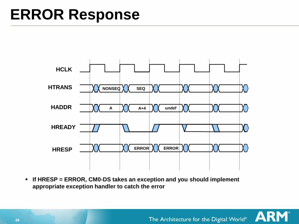
ERROR Response
HCLK
A
ERROR ERROR
NONSEQ SEQ
A+4 undef
HTRANS
HADDR
HREADY
HRESP
If HRESP = ERROR, CM0-DS takes an exception and you should implement
appropriate exception handler to catch the error

50
Agenda
AMBA Family (2)
Introduction to AHB-Lite (6)
AHB-Lite System (8)
AHB-Lite Signals – Master & Slave (15)
AHB-Lite Transactions (9)
How to build a simple AHB-Lite Slave (4)
AHB-Lite – Multilayer Design (3)

51
AHB2LED TOP LEVEL
AHB2LED
Transfer
Response
Read Data
Write Data
Address and
Control
Slave Select
Global SignalLED

52
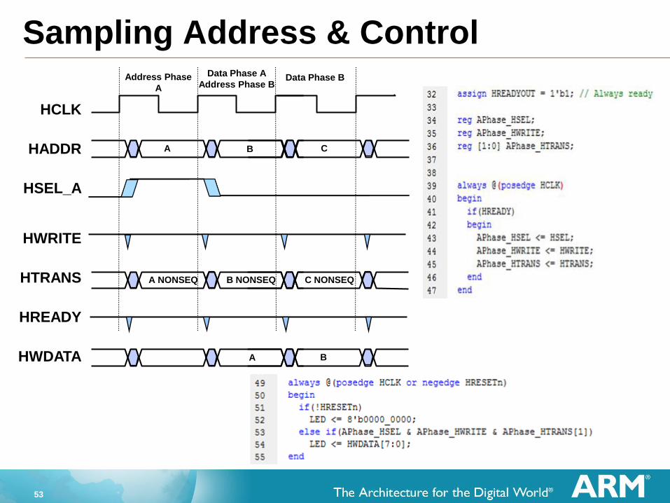
Sampling Address & Control
HCLK
HADDR
HSEL_A
HWRITE
HTRANS
HREADY
Address Phase
A
Data Phase A
Address Phase B
A
Data Phase B
CB
A NONSEQ C NONSEQB NONSEQ
53
Sampling Address & Control
HCLK
HADDR
HSEL_A
HWRITE
HTRANS
HREADY
HWDATA
Address Phase
A
Data Phase A
Address Phase B
A
Data Phase B
CB
A B
A NONSEQ C NONSEQB NONSEQ

54
AHB2LED Verilog Module
Address and Control
Sampling Phase
Data Sampling Phase
One way of implementing

55
BUS MATRIX - ISE

56
Agenda
AMBA Family
Introduction to AHB-Lite
AHB-Lite System
AHB-Lite Signals – Master & Slave
AHB-Lite Transactions
How to build a simple AHB-Lite Slave
AHB-Lite – Advanced

57
Shared Slave
Master 0
Slave
#1
Master 1
Slave
#2
Slave
#3
Slave
#4
Slave Mux
Master 0 can access slaves #1, #2 & #3
Master 1 can access slaves #3 & #4
Contention occurs only if Master 0 & Master 1 try to access slave #3 sametime
Arbitration is at the slave level

58
Multi-layer
ARM
Slave
#1
DMA
Slave
#2
Slave
#3
Slave
#4
Slave
Mux
Slave
Mux
Slave
Mux
Slave
Mux
Generalizing on previous slide
Contention occurs only if Master 0 & Master 1 try to access same slave at
same time
Arbitration is at the slave level

59
Typical Multi-layer example
Master 0
On-chip
RAM
Master 1
External
Memory
I/F
DMA
Slave
Slave
Mux
Slave
Mux
UART Timer GPIO
AHB2APB
Master 0 can access private RAM, APB and external interface
Master 1 can access DMA slave, APB and external interface
60
Further Information
ARM IHI 0033 - AMBA 3 AHB-Lite Protocol Specification
http://infocenter.arm.com/

61
THE END