Embed Size (px)
Citation preview
AFRL-RX-WP-TR-2013-0202
INTEGRATED PHOTONIC CIRCUIT FABRICATION FOR ENABLING RF EMITTER ARRAY F. Kenneth Hopkins AFRL/RXAP Kevin M. Walsh and Alexander Benken University of Louisville SEPTEMBER 2013 Interim Report
Approved for public release; distribution unlimited.
See additional restrictions described on inside pages
STINFO COPY
AIR FORCE RESEARCH LABORATORY MATERIALS AND MANUFACTURING DIRECTORATE
WRIGHT-PATTERSON AIR FORCE BASE, OH 45433-7750 AIR FORCE MATERIEL COMMAND
UNITED STATES AIR FORCE

NOTICE AND SIGNATURE PAGE Using Government drawings, specifications, or other data included in this document for any purpose other than Government procurement does not in any way obligate the U.S. Government. The fact that the Government formulated or supplied the drawings, specifications, or other data does not license the holder or any other person or corporation; or convey any rights or permission to manufacture, use, or sell any patented invention that may relate to them. Qualified requestors may obtain copies of this report from the Defense Technical Information Center (DTIC) (http://www.dtic.mil) AFRL-RX-WP-TR-2013-0202 HAS BEEN REVIEWED AND IS APPROVED FOR PUBLICATION IN ACCORDANCE WITH ASSIGNED DISTRIBUTION STATEMENT. //SIGNED// //SIGNED// ROBERT L. NELSON, Program Manager DANIEL J. BREWER, Chief Photonic Materials Branch Photonic Materials Branch Functional Materials Division //SIGNED// KAREN R. OLSON, Deputy Chief Functional Materials Division Materials & Manufacturing Directorate This report is published in the interest of scientific and technical information exchange and its publication does not constitute the Government’s approval or disapproval of its ideas or findings.

REPORT DOCUMENTATION PAGE Form Approved OMB No. 0704-0188
The public reporting burden for this collection of information is estimated to average 1 hour per response, including the time for reviewing instructions, searching existing data sources, gathering and maintaining the data needed, and completing and reviewing the collection of information. Send comments regarding this burden estimate or any other aspect of this collection of information, including suggestions for reducing this burden, to Department of Defense, Washington Headquarters Services, Directorate for Information Operations and Reports (0704-0188), 1215 Jefferson Davis Highway, Suite 1204, Arlington, VA 22202-4302. Respondents should be aware that notwithstanding any other provision of law, no person shall be subject to any penalty for failing to comply with a collection of information if it does not display a currently valid OMB control number. PLEASE DO NOT RETURN YOUR FORM TO THE ABOVE ADDRESS.
1. REPORT DATE (DD-MM-YY) 2. REPORT TYPE 3. DATES COVERED (From - To) September 2013 Interim 27 August 2012 – 31 August 2013
4. TITLE AND SUBTITLE
INTEGRATED PHOTONIC CIRCUIT FABRICATION FOR ENABLING RF EMITTER ARRAY
5a. CONTRACT NUMBER
In-House 5b. GRANT NUMBER 5c. PROGRAM ELEMENT NUMBER
62102F 6. AUTHOR(S)
F. Kenneth Hopkins (AFRL/RXAP) Kevin M. Walsh and Alexander Benken (University of Louisville)
5d. PROJECT NUMBER
4347 5e. TASK NUMBER
5f. WORK UNIT NUMBER
X09B (PS114100) 7. PERFORMING ORGANIZATION NAME(S) AND ADDRESS(ES) 8. PERFORMING ORGANIZATION
REPORT NUMBER
AFRL/RXAP 3005 Hobson Way Wright-Patterson AFB, OH 45433
University of Louisville Electrical & Computer Engineering Louisville, KY 40292
9. SPONSORING/MONITORING AGENCY NAME(S) AND ADDRESS(ES)
Air Force Research Laboratory Materials and Manufacturing Directorate Wright-Patterson Air Force Base, OH 45433-7750 Air Force Materiel Command United States Air Force
10. SPONSORING/MONITORING AGENCY ACRONYM(S)
AFRL/RXAP 11. SPONSORING/MONITORING AGENCY REPORT NUMBER(S)
AFRL-RX-WP-TR-2013-0202
12. DISTRIBUTION/AVAILABILITY STATEMENT
Approved for public release; distribution is unlimited.
13. SUPPLEMENTARY NOTES
Approved by 88ABW Public Affairs Office: Case number 88ABW-2013-4657 on 06-Nov-13. Report contains color. 14. ABSTRACT
The interim report describes an initial effort to fabricate an Integrated Photonic Circuit (IPC) which provides a means for converting an optical laser signal, that consists of both a narrow-line carrier wavelength and a heterodyned RF signal that are in-phase, to an electrical RF signal that can drive various on-chip components such as an antenna. The IPC would supply a critical missing element for enabling new phased-array radar based on an all-optical architecture. Ge-on-Si technology, the focus of the effort, has specific advantages that are fundamental to nearly all integrated photonic circuits. Its direct energy bandgap, slightly larger than Ge’s indirect bandgap, permits band-to-band recombination/generation at an energy that corresponds to light near the standard optical communications wavelength. Ge-on-Si technology, therefore, could enable a host of IPC subcomponents including photodetectors, laser diodes, and enhanced silicon modulators. In addition, such germanium devices can be simply and inexpensively incorporated into a silicon manufacturing process.
15. SUBJECT TERMS
integrated photonics, germanium, photodetector, heterodyne detector 16. SECURITY CLASSIFICATION OF: 17. LIMITATION
OF ABSTRACT:
SAR
18. NUMBER OF PAGES
23
19a. NAME OF RESPONSIBLE PERSON (Monitor)
a. REPORT
Unclassified
b. ABSTRACT
Unclassified
c. THIS PAGE
Unclassified
Robert L. Nelson 19b. TELEPHONE NUMBER (Include Area Code)
(937) 255-9904 Standard Form 298 (Rev. 8-98)
Prescribed by ANSI Std. Z39-18
i Approved for public release; distribution unlimited
TABLE OF CONTENTS Section Page List of Figures ................................................................................................................................. ii List of Tables .................................................................................................................................. ii 1.0 INTRODUCTION ..................................................................................................................1 2.0 APPROACHES.......................................................................................................................3
2.1 NONLINEAR OPTICAL WAVEGUIDE .....................................................................3 2.2 PHOTODETECTOR .....................................................................................................4
3.0 COMPONENT DESIGN ........................................................................................................6 3.1 OPTICAL FIBER MOUNT .........................................................................................6 3.2 PHOTODETECTOR ....................................................................................................8
4.0 FABRICATION ....................................................................................................................11 4.1 GERMANIUM DEPOSITION ..................................................................................11 4.2 SELECTIVE ETCHING OF GERMANIUM ............................................................12 4.3 PHOTODETECTOR ..................................................................................................13
5.0 CONCLUSION .....................................................................................................................16 6.0 REFERENCES .....................................................................................................................17 7.0 LIST OF ACRONYMS, ABBREVIATIONS, AND SYMBOLS .......................................18
ii Approved for public release; distribution unlimited
LIST OF FIGURES Figure Page 1 Photonic approach to RF phased-array ....................................................................................2 2 Typical responsivity of Ge and InGaAs photodiodes ..............................................................5 3 Ge phototransistor .....................................................................................................................5 4 Potential architecture for v-groove/photodetector integration .................................................6 5 V-groove / fiber geometry ........................................................................................................7 6 Panda style optical fiber ...........................................................................................................7 7 Ge photodiode ...........................................................................................................................8 8 Current-voltage characteristic of p-type Ge on n-type Si .........................................................9 9 Germanium photodiode on a Si substrate ...............................................................................10 10 Activated electron concentrations (n) in Ge after implantation and annealing ......................11 11 X-ray diffraction spectra comparing Ge films .......................................................................11 12 Micrograph of the Ge surface after selective etching in heated H2O2 ....................................12 13 Test photolithographic mask ..................................................................................................13 14 Plots from L-Edit files for Ge-on-Si photodetector ................................................................15 15 Semiconductor test structures .................................................................................................15
LIST OF TABLES Table Page 1 Experimental results for selective wet etching of Ge .............................................................13 2 Semiconductor fabrication schedule ......................................................................................14
1 Approved for public release; distribution unlimited.
Approved by 88ABW Public Affairs Office: Case number 88ABW-2013-4657 on 06-Nov-13.
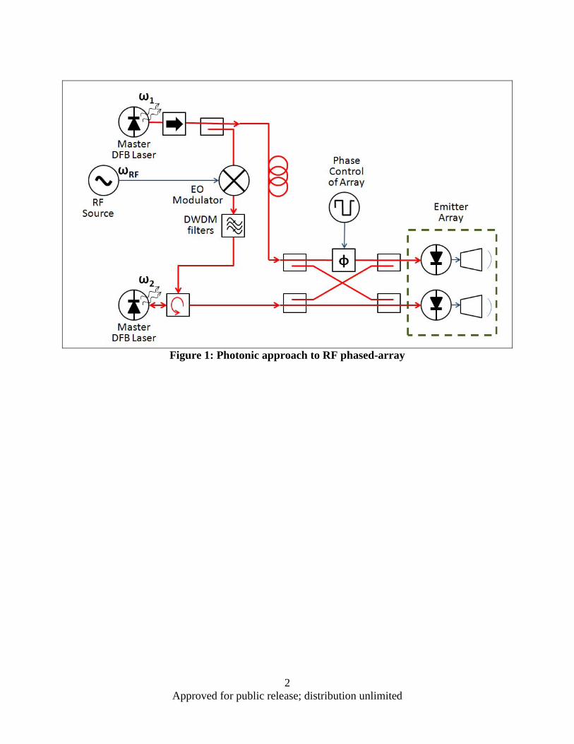
1.0 INTRODUCTION During the 1990’s, many radar experts understood that very large phased-array radar on either aircraft or space platforms could only be realized with photonic control utilizing high bandwidth optical fiber, electro-optic (EO) modulators, and optical detectors. The approach promised significant savings in the radar system’s size, weight, and power as compared with all-electronic approaches. This early photonic development effort utilized amplitude modulation to encode information on a laser carrier, and unfortunately, the linear dynamic range of an electro-optic modulator is extremely limited. In other words, the approach was not feasible. Yet, the effort served to encourage the development of new materials that are now proving to be transformational. A new photonic approach was recently proposed that utilizes phase modulation versus amplitude modulation. [1] It utilizes (a) polarized single mode fiber, (b) EO modulators for wavelength mixing of optical and electronic signals (ω2=ωC+ωRF) for which the carrier frequency (ωC) is coherently phase-locked to the sideband frequency (ω2), and (c) photodetectors for heterodyne detection (for a photodiode, current =DC component + ωRF component). A schematic of the basic approach is illustrated in Figure 1, showing the control of two pixels of a phased-array emitter. The technical objective of the research described in this report is to investigate materials and materials structures to enable an integrated photonic circuit optical heterodyne detection for driving an antenna element of a phased array. Two approaches were considered to enable a compact and efficient heterodyne detector that is coupled to an antenna, heterodyne detection utilizing either a second-order nonlinear optical waveguide or a photodetector. Two precepts should be recognized regarding integrated photonic circuits. First, IPCs require a common substrate, for which silicon has recognized advantages. Commercially available silicon wafers are large, inexpensive, offer extreme flatness for optical components, excellent electronic properties for integration with electronic devices, compatibility with many epitaxial materials, and potential for simple integration with optical fiber using v-groove fabrication. Second, IPC operation at a 1.55 µm wavelength has advantages for compatibility with optical communications systems and subcomponents already developed for the optical communications industry.
2 Approved for public release; distribution unlimited
Figure 1: Photonic approach to RF phased-array
3 Approved for public release; distribution unlimited
2.0 APPROACHES Optical heterodyne detection refers to the conversion of laser light made up of an optical or carrier frequency (ωC) that is modulated at frequency (ωRF) and to an electrical signal at ωRF for driving electronic components. In this case, the component is a micro-antenna, an element of a phased array antenna, and possibly associated electronics that interface the heterodyne detector to the antenna. Two approaches to heterodyne detection were compared under the task. The first approach utilizes a nonlinear optical waveguide, and the second uses a photodetector. 2.1 Nonlinear Optical Waveguide In the first approach, a second-order nonlinear-optical polymer waveguide is utilized for converting the modulated optical signal to a voltage to drive the antenna element. The waveguide concentrates the laser light for efficient generation of a ωRF term that appears as a voltage across the waveguide. If electrodes are placed across this region of the waveguide, then the electrodes can be directly connected to the antenna element or its associated electronic components. The conversion of the modulated optical signal to the RF electrical signal is easily derived. Assume that the electric field E of the optical signal is composed of two components, E1 at frequency ωc and E2 at ωRF. The electric polarization (P) across the guide is then:
)( 22EEP o χχε +≅
221221 ])cos(cos[])cos(cos[ tEtEtEtE RFccoRFcco ωωωχεωωωχε +++++=
])cos(cos[ 211 tEtE RFcco ωωωχε ++=
]})2cos([cos])(2cos21
21[)2cos
21
21({ 21
22
212 ttEEtEtE RFcRFRFcco ωωωωωωχε ++++++++ (1)
It is assumed in equation (1) that higher order nonlinear susceptibilities for the material beyond χ2 are negligible, and εo is the permittivity of free space. The expression clearly shows that the nonlinear optical waveguide generates a ωRF term. The approach was proposed in 1998 and fully demonstrated in 2005. [2,3] There are a number of advantages and disadvantages to this as compared with a photovoltaic detector approach, one advantage being RF frequency responses to 400 GHz. [4] Yet, potential responsivities are unreasonably low, on the order of 9 mA/W for optimal performance. [4] The extremely low potential performance is sufficient justification to not further investigate this approach. 2.2 Photodetector In the second approach, a photodetector such as a photodiode operating in the photovoltaic regime detects the laser light. The resulting signal either directly or indirectly drives the antenna element of a phased array. If the photodiode is biased such that the voltage across the junction is less than the thermal voltage, kT/q, the current from the photodiode is given by
4 Approved for public release; distribution unlimited
ntphotocurretdarkcurrendiode III +=
sAQq
mkTqVC η−−≅ ]1)[exp(
2
4]1)[exp( EAq
kTqVC o
πηλε
−−≅ (2)
where the dark current is assumed to be dominated by the bulk diffusion current, where QS is the photon flux of the laser light entering the depletion region of the photodiode, and where the electric field associated with the laser light is E. In addition, q is the charge on an electron, λ is the wavelength of light, εo is the permittivity of free space, A is the area of the detector, and is Planck’s constant over 2π. The E2 expression in equation (2) can be expanded in the following manner to show how the ωRF term is generated. 2
212 }])cos{(}cos{[ tEtEE RFcc ωωω ++=
}cos{4
})2cos{(4
})(2cos{2
}2cos{222
21212
22
12
22
1 tEEtEEtEtEEERFRFcRFcc ωωωωωω +++++++= (3)
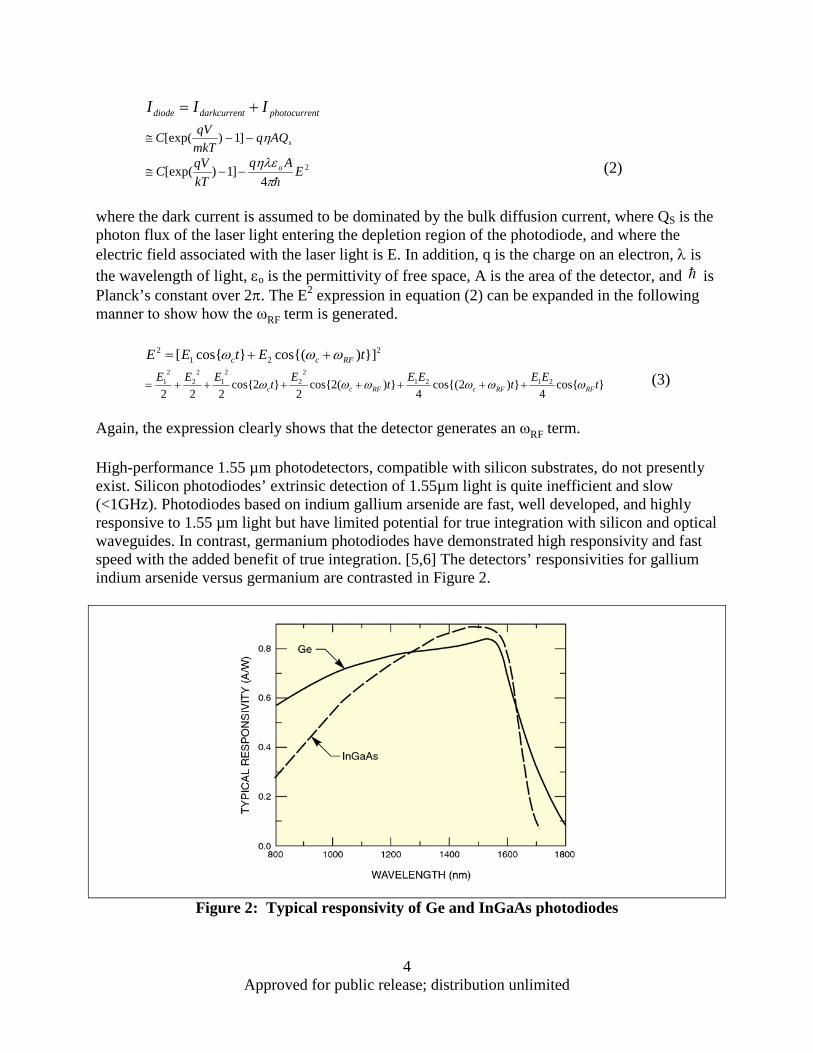
Again, the expression clearly shows that the detector generates an ωRF term. High-performance 1.55 µm photodetectors, compatible with silicon substrates, do not presently exist. Silicon photodiodes’ extrinsic detection of 1.55µm light is quite inefficient and slow (<1GHz). Photodiodes based on indium gallium arsenide are fast, well developed, and highly responsive to 1.55 µm light but have limited potential for true integration with silicon and optical waveguides. In contrast, germanium photodiodes have demonstrated high responsivity and fast speed with the added benefit of true integration. [5,6] The detectors’ responsivities for gallium indium arsenide versus germanium are contrasted in Figure 2.
Figure 2: Typical responsivity of Ge and InGaAs photodiodes
5 Approved for public release; distribution unlimited
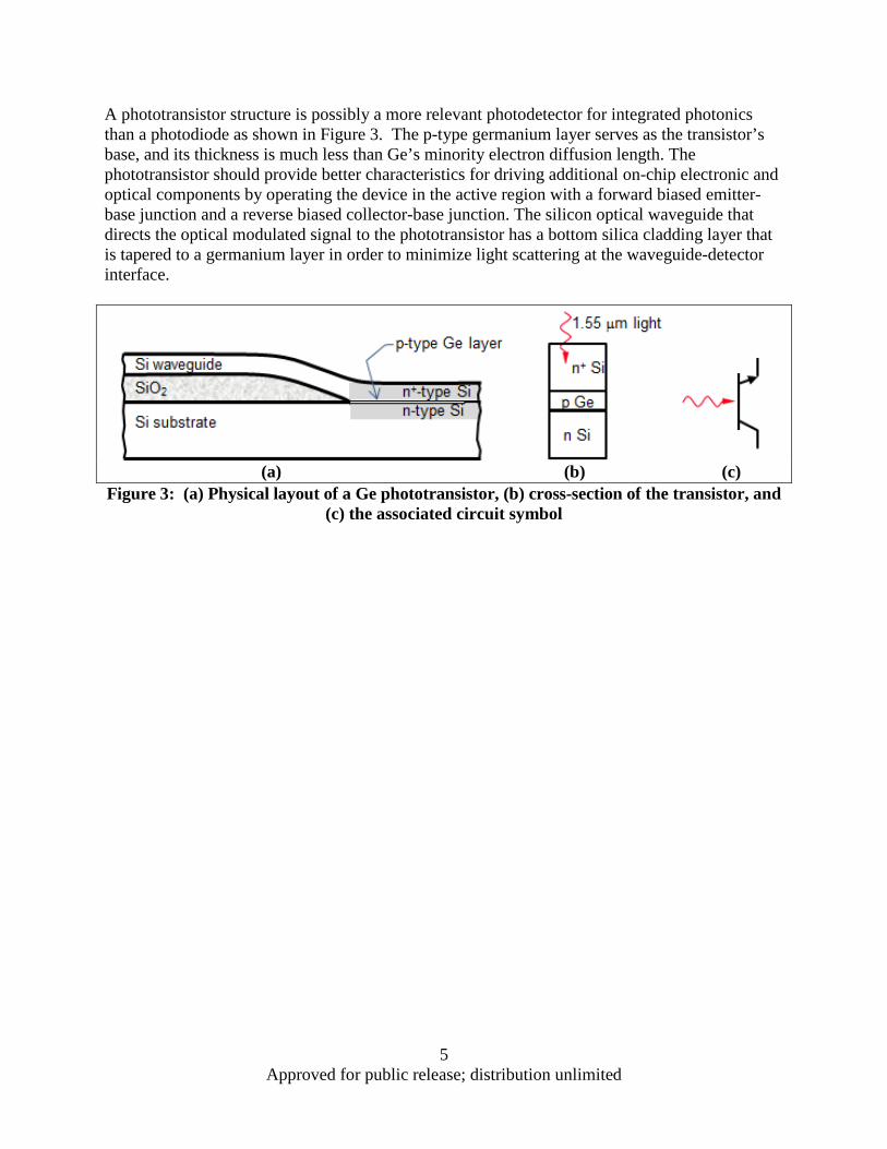
A phototransistor structure is possibly a more relevant photodetector for integrated photonics than a photodiode as shown in Figure 3. The p-type germanium layer serves as the transistor’s base, and its thickness is much less than Ge’s minority electron diffusion length. The phototransistor should provide better characteristics for driving additional on-chip electronic and optical components by operating the device in the active region with a forward biased emitter-base junction and a reverse biased collector-base junction. The silicon optical waveguide that directs the optical modulated signal to the phototransistor has a bottom silica cladding layer that is tapered to a germanium layer in order to minimize light scattering at the waveguide-detector interface.
(a) (b) (c) Figure 3: (a) Physical layout of a Ge phototransistor, (b) cross-section of the transistor, and
(c) the associated circuit symbol
6 Approved for public release; distribution unlimited
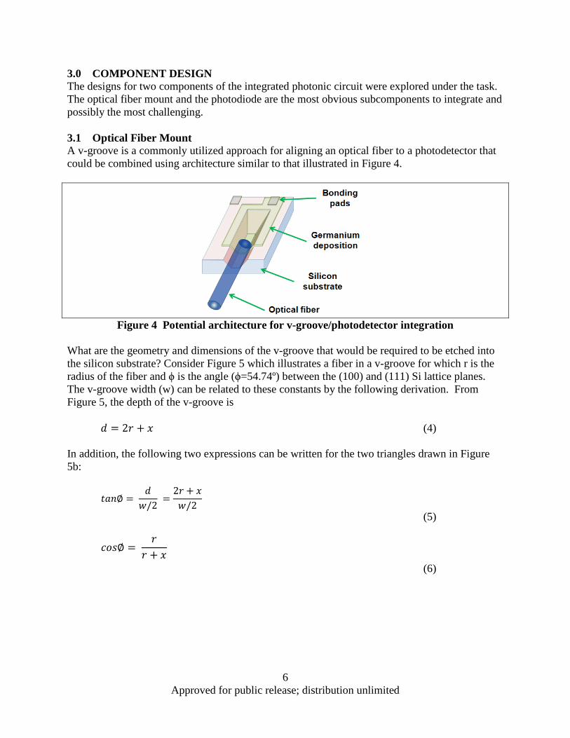
3.0 COMPONENT DESIGN The designs for two components of the integrated photonic circuit were explored under the task. The optical fiber mount and the photodiode are the most obvious subcomponents to integrate and possibly the most challenging. 3.1 Optical Fiber Mount A v-groove is a commonly utilized approach for aligning an optical fiber to a photodetector that could be combined using architecture similar to that illustrated in Figure 4.
Figure 4 Potential architecture for v-groove/photodetector integration
What are the geometry and dimensions of the v-groove that would be required to be etched into the silicon substrate? Consider Figure 5 which illustrates a fiber in a v-groove for which r is the radius of the fiber and ϕ is the angle (ϕ=54.74º) between the (100) and (111) Si lattice planes. The v-groove width (w) can be related to these constants by the following derivation. From Figure 5, the depth of the v-groove is 𝑑𝑑 = 2𝑟𝑟 + 𝑥𝑥 (4) In addition, the following two expressions can be written for the two triangles drawn in Figure 5b:
𝑡𝑡𝑡𝑡𝑡𝑡∅ = 𝑑𝑑𝑤𝑤/2
=2𝑟𝑟 + 𝑥𝑥𝑤𝑤/2
(5)
𝑐𝑐𝑐𝑐𝑐𝑐∅ = 𝑟𝑟
𝑟𝑟 + 𝑥𝑥
(6)
7 Approved for public release; distribution unlimited
(a) (b)
Figure 5: V-groove / fiber geometry Combining these equations and solving for w, the following results: 𝑤𝑤 = 2𝑟𝑟(cot∅ + csc∅) (7) The radius of the fiber was obtained by contacting the company, Phase Sensitive Innovations, Inc. of Newark, DE. The company is presently helping AFRL to demonstrate the photonic-controlled RF emitter system for which the present task could enable a potential component. Dr. Christopher Schuetz of Phase Sensitive Innovations is using a standard phase-maintaining Panda optical fiber (see Figure 6) for the demonstration. It is available from Thorlabs (item # PM1550-HP). The outer diameter of the fiber is 125±1 µm.
Figure 6: Panda style optical fiber
Using the maximum diameter of the fiber (126 µm) in the equation above, the v-groove width is calculated to be 241.5 µm. In addition, the etch depth could range from 2r (126 µm) to 2r+x (171 µm). A value of 130 µm is perhaps an ideal target for the etch depth. For v-groove fabrication using a KOH etchant at 85ºC, the silicon etch time would then be (130 µm)/( 1.4µm/min) = 93 minutes. 3.2 Photodetector The initial design of a Ge-on-Si photodiode under this task entails the deposition of a few nanometer thick Ge layer on a Si (100) n-type substrate followed by a shallow phosphorous implantation extending into the silicon, activation annealing, and thick Ge growth. Defects in the thick Ge film provide effective p-type doping. [7] This test photodiode structure is illustrated in Figure 7.
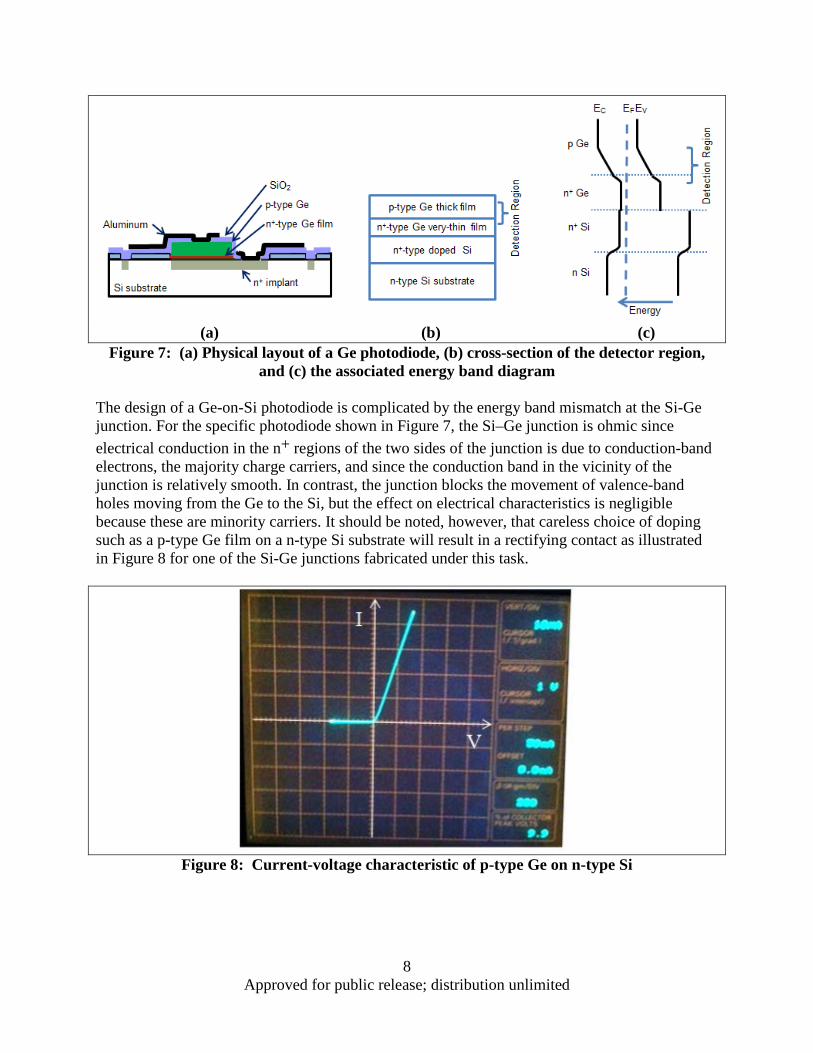
8 Approved for public release; distribution unlimited
(a) (b) (c)
Figure 7: (a) Physical layout of a Ge photodiode, (b) cross-section of the detector region, and (c) the associated energy band diagram
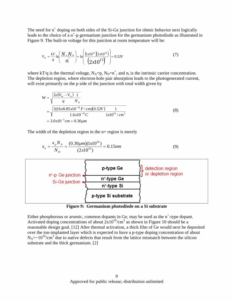
The design of a Ge-on-Si photodiode is complicated by the energy band mismatch at the Si-Ge junction. For the specific photodiode shown in Figure 7, the Si–Ge junction is ohmic since electrical conduction in the n+ regions of the two sides of the junction is due to conduction-band electrons, the majority charge carriers, and since the conduction band in the vicinity of the junction is relatively smooth. In contrast, the junction blocks the movement of valence-band holes moving from the Ge to the Si, but the effect on electrical characteristics is negligible because these are minority carriers. It should be noted, however, that careless choice of doping such as a p-type Ge film on a n-type Si substrate will result in a rectifying contact as illustrated in Figure 8 for one of the Si-Ge junctions fabricated under this task.
Figure 8: Current-voltage characteristic of p-type Ge on n-type Si
9 Approved for public release; distribution unlimited
The need for n+ doping on both sides of the Si-Ge junction for ohmic behavior next logically leads to the choice of a n+-p germanium junction for the germanium photodiode as illustrated in Figure 9. The built-in voltage for this junction at room temperature will be:
( )( )( ) Vxx
qkT
xnNNi
DAbi 52.0
13102101lnlnV
1022
1916
2 =
=
= (7)
where kT/q is the thermal voltage, NA=p, ND=n+, and ni is the intrinsic carrier concentration. The depletion region, where electron-hole pair absorption leads to the photogenerated current, will exist primarily on the p side of the junction with total width given by
( )
( )
mcmxcmxCx
VcmFxx
NqVV
A
Abi
µ
ε
30.0100.3/101
1106.1
52.0)/1085.816(2
12W
5
31619
14
==
=
−=
−
−
− (8)
The width of the depletion region in the n+ region is merely
nmx
xmN
Nxx
D
Apn 15.0
)102()101)(30.0(
19
16
===µ
(9)
Figure 9: Germanium photodiode on a Si substrate
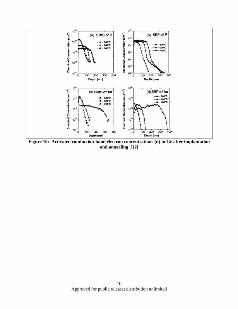
Either phosphorous or arsenic, common dopants in Ge, may be used as the n+-type dopant. Activated doping concentrations of about 2x10¹⁹/cm3 as shown in Figure 10 should be a reasonable design goal. [12] After thermal activation, a thick film of Ge would next be deposited over the ion-implanted layer which is expected to have a p-type doping concentration of about NA=~1016/cm3 due to native defects that result from the lattice mismatch between the silicon substrate and the thick germanium. [2]
10 Approved for public release; distribution unlimited
Figure 10: Activated conduction-band electron concentrations (n) in Ge after implantation
and annealing [12]
11 Approved for public release; distribution unlimited
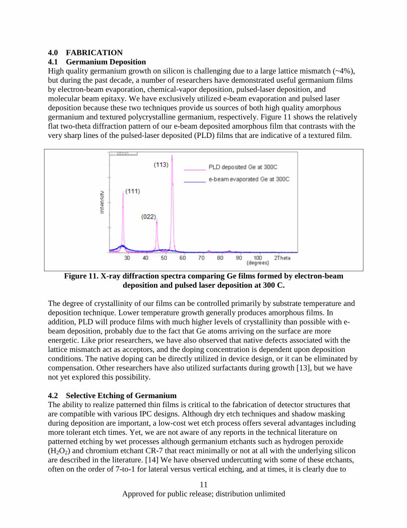
4.0 FABRICATION 4.1 Germanium Deposition High quality germanium growth on silicon is challenging due to a large lattice mismatch (~4%), but during the past decade, a number of researchers have demonstrated useful germanium films by electron-beam evaporation, chemical-vapor deposition, pulsed-laser deposition, and molecular beam epitaxy. We have exclusively utilized e-beam evaporation and pulsed laser deposition because these two techniques provide us sources of both high quality amorphous germanium and textured polycrystalline germanium, respectively. Figure 11 shows the relatively flat two-theta diffraction pattern of our e-beam deposited amorphous film that contrasts with the very sharp lines of the pulsed-laser deposited (PLD) films that are indicative of a textured film.
Figure 11. X-ray diffraction spectra comparing Ge films formed by electron-beam
deposition and pulsed laser deposition at 300 C. The degree of crystallinity of our films can be controlled primarily by substrate temperature and deposition technique. Lower temperature growth generally produces amorphous films. In addition, PLD will produce films with much higher levels of crystallinity than possible with e-beam deposition, probably due to the fact that Ge atoms arriving on the surface are more energetic. Like prior researchers, we have also observed that native defects associated with the lattice mismatch act as acceptors, and the doping concentration is dependent upon deposition conditions. The native doping can be directly utilized in device design, or it can be eliminated by compensation. Other researchers have also utilized surfactants during growth [13], but we have not yet explored this possibility. 4.2 Selective Etching of Germanium The ability to realize patterned thin films is critical to the fabrication of detector structures that are compatible with various IPC designs. Although dry etch techniques and shadow masking during deposition are important, a low-cost wet etch process offers several advantages including more tolerant etch times. Yet, we are not aware of any reports in the technical literature on patterned etching by wet processes although germanium etchants such as hydrogen peroxide (H2O2) and chromium etchant CR-7 that react minimally or not at all with the underlying silicon are described in the literature. [14] We have observed undercutting with some of these etchants, often on the order of 7-to-1 for lateral versus vertical etching, and at times, it is clearly due to
12 Approved for public release; distribution unlimited
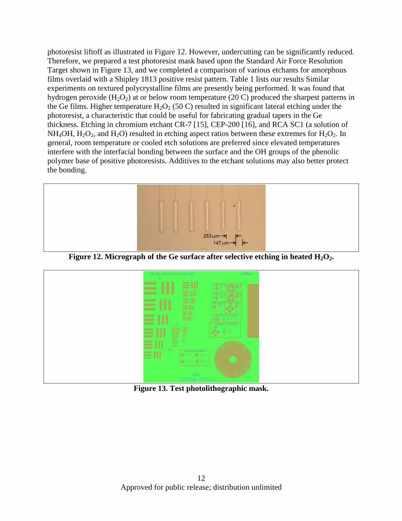
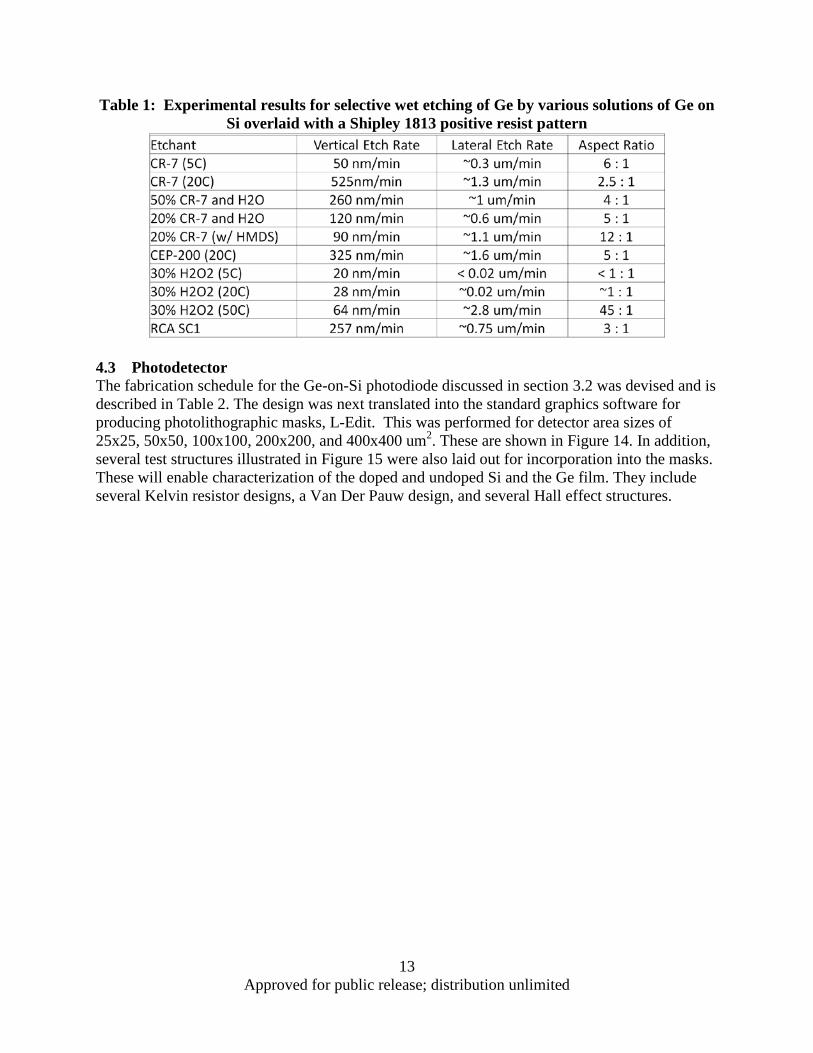
photoresist liftoff as illustrated in Figure 12. However, undercutting can be significantly reduced. Therefore, we prepared a test photoresist mask based upon the Standard Air Force Resolution Target shown in Figure 13, and we completed a comparison of various etchants for amorphous films overlaid with a Shipley 1813 positive resist pattern. Table 1 lists our results Similar experiments on textured polycrystalline films are presently being performed. It was found that hydrogen peroxide (H2O2) at or below room temperature (20 C) produced the sharpest patterns in the Ge films. Higher temperature H2O2 (50 C) resulted in significant lateral etching under the photoresist, a characteristic that could be useful for fabricating gradual tapers in the Ge thickness. Etching in chromium etchant CR-7 [15], CEP-200 [16], and RCA SC1 (a solution of NH4OH, H2O2, and H2O) resulted in etching aspect ratios between these extremes for H2O2. In general, room temperature or cooled etch solutions are preferred since elevated temperatures interfere with the interfacial bonding between the surface and the OH groups of the phenolic polymer base of positive photoresists. Additives to the etchant solutions may also better protect the bonding.
Figure 12. Micrograph of the Ge surface after selective etching in heated H2O2.
Figure 13. Test photolithographic mask.
13 Approved for public release; distribution unlimited
Table 1: Experimental results for selective wet etching of Ge by various solutions of Ge on Si overlaid with a Shipley 1813 positive resist pattern
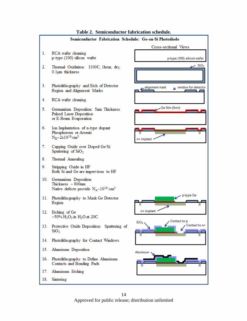
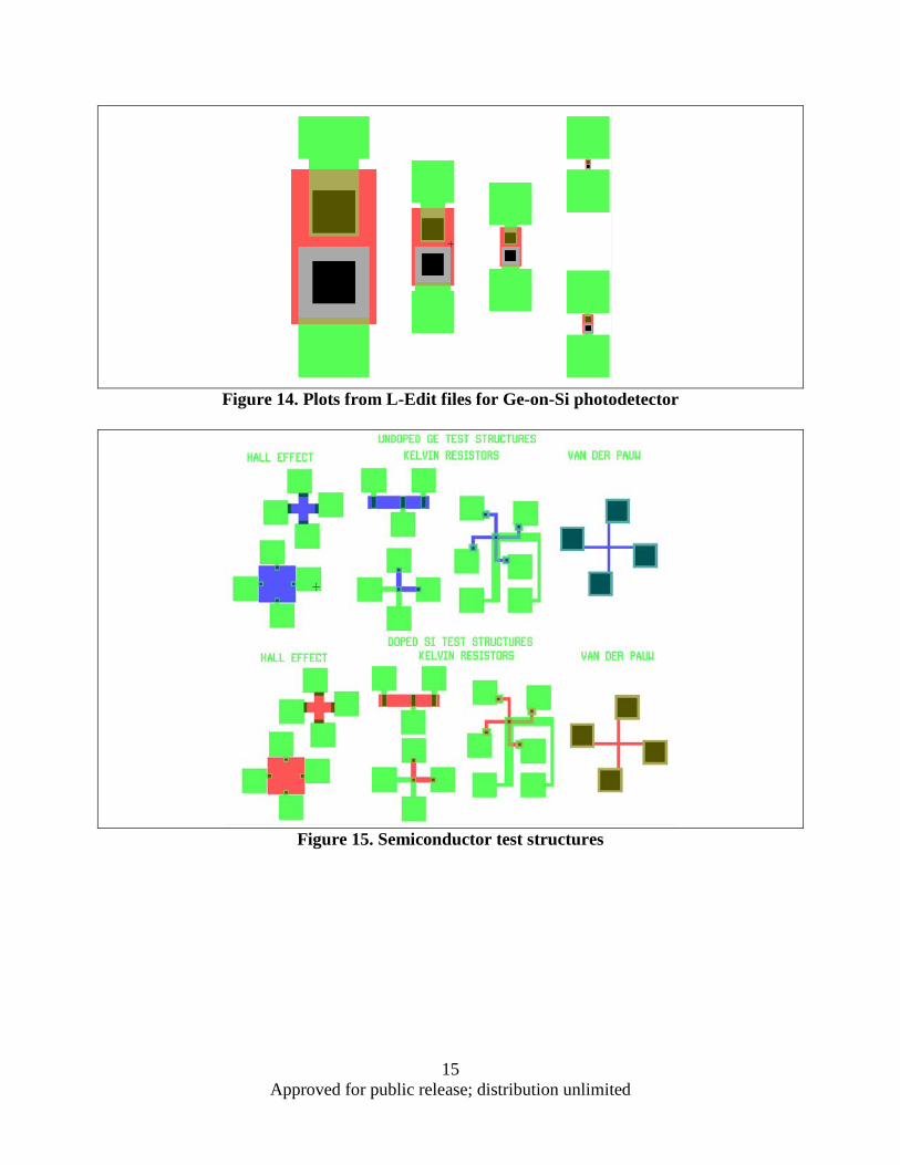
4.3 Photodetector The fabrication schedule for the Ge-on-Si photodiode discussed in section 3.2 was devised and is described in Table 2. The design was next translated into the standard graphics software for producing photolithographic masks, L-Edit. This was performed for detector area sizes of 25x25, 50x50, 100x100, 200x200, and 400x400 um2. These are shown in Figure 14. In addition, several test structures illustrated in Figure 15 were also laid out for incorporation into the masks. These will enable characterization of the doped and undoped Si and the Ge film. They include several Kelvin resistor designs, a Van Der Pauw design, and several Hall effect structures.
14 Approved for public release; distribution unlimited
Table 2. Semiconductor fabrication schedule.
15 Approved for public release; distribution unlimited
Figure 14. Plots from L-Edit files for Ge-on-Si photodetector
Figure 15. Semiconductor test structures
16 Approved for public release; distribution unlimited
5.0 CONCLUSION In summary, germanium-on-silicon is a promising technology for enabling an integrated photonic circuit utilizing optical heterodyne detection for driving an antenna element of a phased array. Our study concluded that a photodetector is the preferred approach over utilizing a second-order nonlinear optical waveguide for heterodyne detection. We then proceeded to design a photodetector, and then began studying the processes for fabricating it. Also, we discovered that information for one of the critical processing steps, selective etching of Ge on Si, is not available in the world’s technical literature. After a comparative study of processes, we concluded that either room temperature or cooled hydrogen peroxide was the optimum selective etchant. We have also concluded that Ge-on-Si technology has specific advantages that are fundamental to nearly all integrated photonic circuits. [17] Its direct energy bandgap, slightly larger than Ge’s indirect bandgap, permits band-to-band recombination/generation at an energy that corresponds to light near the optical communications wavelength of 1.55 µm, which could enable a host of IPC subcomponents including photodetectors, laser diodes, and enhanced silicon modulators. In addition, such germanium devices can be simply and inexpensively incorporated into a silicon manufacturing process.
17 Approved for public release; distribution unlimited
6.0 REFERENCES 1. Schuetz, C.A., R.D. Martin, E.E. Dillon, S. Shi, & D.W. Prather, “Optical Techniques for Multifunctional Millimeter-Wave Imaging Receivers,” IEEE Photonics Conf (PHO) 823-824 (2011) 2. Nahata, A. and T.F. Heinz, “Generation of subpicosecond electrical pulses by optical rectification,” Optics Letters 23, 867-869 (1998). 3. Baehr-Jones, T., M. Hochberg, G. Wang, R. Lawson, Y. Liao, P.A. Sullivan, L. Dalton, A.K.-Y. Jen, & A. Scherer, “Optical modulation and detection in slotted Silicon waveguides,” OPTICS EXPRESS 13, 5216 (11 July 2005). 4. Baehr-Jones, T., J. Witzens, & M. Hochberg, “Theoretical Study of Optical Rectification at Radio Frequencies in a Slot Waveguide,” IEEE Journal of Quantum Electronics 46, 1634 (11 Nov 2010). 5. Duan, N. et al., “310GHz gain-bandwidth product Ge/Si avalanche photodetector for 1550nm light detection,” Opt. Express 20, 11031–11036 (2012). 6. Chen, L., C.R. Doerr, L. Buhl, Y. Baeyens, and R.A. Aroca, “Monolithically integrated 40-wavelength demultiplexer and photodetector array on silicon,” IEEE Photonic Tech. L. 23, 869-871 (2011). 7. Oh, J., S.K. Banerjee, and J.C. Campbell, “Metal-Germanium-Metal Photodetectors on Heteroepitaxial Ge-on-Si With Amorphous Ge Schottky Barrier Enhancement Layers,” IEEE Photonics Tech. L. 16, 581-583 (2004). 8. Wietler, T.F., A. Ott, E. Bugiel, K.R. Hofmann, “Advances in surfactant-mediated growth of germanium on silicon: high-quality p-type Ge films on Si,” Mat. Sci. in Semicon. Proc. 8, 73 (2005). 9. Williams, K.R., K. Gupta, and M. Wasilik, “Etch Rates for Micromachining Processing—Part II” J. Microelectromech. S. 12, 761 (Dec 2003). 10. http://www.cyantek.com/chrome-etchants.php (30 May 2013). 11. http://www.microchrometechnology.com/products_hardsurface.php (30 May 2013). 12. Chui, C.O., L. Kulig, J. Moran, W. Tsai, and K.C. Saraswat, “Germanium n-type shallow junction activation dependences,” Applied Physics Letters 87, 091909 (2005) 13. Wietler, T.F., A. Ott, E. Bugiel, K.R. Hofmann, “Advances in surfactant-mediated growth of germanium on silicon: high-quality p-type Ge films on Si,” Mat. Sci. in Semicon. Proc. 8, 73 (2005) 14. Williams, K.R., K. Gupta, and M. Wasilik, “Etch Rates for Micromachining Processing—Part II” J. Microelectromech. S. 12, 761 (Dec 2003) 15. http://www.cyantek.com/chrome-etchants.php (30 May 2013) 16. http://www.microchrometechnology.com/products_hardsurface.php (30 May 2013) 17. Hopkins, F. K., K. M. Walsh, A. Benken, J. Jones, K. Averett, D. Diggs, L.-S. Tan, S. Mou, and J.G. Grote, “Germanium on silicon to enable integrated photonic circuits,” Proc. SPIE 8876, 8876–30 (2013)

18 Approved for public release; distribution unlimited
Approved by 88ABW Public Affairs Office: Case number 88ABW-2013-4657 on 06-Nov-13.
LIST OF ACRONYMS, ABBREVIATIONS, AND SYMBOLS
Acronym Definition EO Electro-Optic IPC Integrated Photonic Circuit RF Radio Frequency Ge Germanium Si Silicon PLD Pulsed-Laser Deposition H2O2 Hydrogen Peroxide