Embed Size (px)
Citation preview
Abstract—In high-performance computing systems, each
computing node communicates via a high-speed serial bus toensure sufficient data transfer bandwidth. However, eachcomputing node of different bus protocols is very difficult tocommunicate directly, which is not conducive to theextensibility of HPC (High performance computing) clusters. Inthis paper, we propose UPI, a inter-node communicationinterface based on FPGA, which can transmit different busprotocols (PCIe protocol and Ethernet protocol) simultaneously.More importantly, many different bus-supported computingnodes can be connected to the same HPC system. Weimplemented our UPI system on “Gemini” prototypeverification board with two Xilinx Virtex-6 FPGAs. The resultsshow that the transmission speed of the UPI can reach11.04Gpbs (PCIe Gen2 X4) and 4.32Gpbs (Gigabit Ethernet)when DMA payload sizes is greater than 260KB and 80KB,respectively.
Keyword—FPGA-based SoCs, PCIE, Gigabit Ethernet, HPC
I. INTRODUCTIONith the rapid development of high-performanceFPGA-based devices, high-performance computing
system performance bottleneck has shifted from the ability ofsingle node to the architecture of the HPC clusters. In thesystem-level or board-level interconnect system, high-speedserial bus technology with its enormous advantage is rapidlyreplacing traditional parallel bus technology and becomingthe main technology of high-speed FPGA-based SoC design.As the applications of the high-speed serial bus technologygradually expand to all research area, more and more articlesfocus on the technology, especially the multi-nodeinterconnect technology and the high-speed I/O interfacetechnology.
———————————————————————Manuscript received February 24, 2016. This work is a follow up of
the invited journal of the accepted conference paper for the 18thInternational Conference on Advanced Communication Technology. Thisresearch was supported by the “Strategic Priority Research Program” of theChinese Academy of Sciences, Grant No.XDA06010402-4.
An Wu is with the Department of Physics, University of Science andTechnology of China, Hefei, Anhui Province, China (corresponding authorto provide phone: +86-159-5510-2092; e-mail: wuan@ mail.ustc.edu.cn).
Xi Jin is with the Department of Physics, University of Science andTechnology of China, China (e-mil:[email protected]).
XueLiang Du is with the Department of System verification, ChineseAcademy of Science Institute of Automation, China (e-mil:[email protected]).
Shuaizhi Guo is with the Department of Physics, University of Scienceand Technology of China, China (e-mil:[email protected]).
Effective inter-node communication is receivingsignificant attention due to its increasingly importantapplications in high-performance computing, thus inter-nodeinterconnection technology is drawing lots of attractionsfrom more and more researchers. The interconnectionmethods are based on three main protocols: PCIe, Ethernet,and Serial RapidIO (SRIO). However, they have their ownusing domain. They can't communicate each other directly,and for the same reason, each computing node can't becompatible on the means of communication.
In order to achieve a good compatibility between theseprotocols, many problems cannot be neglected. For example,different bus communication requires bridging conversion,the process is complicated and performance loss is hard toavoid. The problem appears in these bus controllers'hardware design. In FPGA-based SoCs, both of Ethernetcontroller and PCIe controller have an external physical layer(PHY) chip. The controllers' PHY chip of mentioned threetypes are different, mainly due to its PHY's interface signalsand communication speeds are not identical. Ethernet PHYchip mainly realizes 64b/66b encoding (Gigabit Ethernet),and PCIe PHY chip completes the 8b/10b encoding (PCIe 2.0and below). However, they still have a lot in common, e.g.,scrambling and parallel-to-serial conversion all need to beimplemented in PHY chip.
The simplest way to solve the compatibility issue is to addall these bus protocols to a computing node, but it requiresmore PHY chips, differential pairs and hardware resources. Abetter approach is to communicate with these computingnodes through the same interface without changing theinterface types. Generally, the physical layer of PCIe,Ethernet and SRIO cannot be shared. We try to merge thephysical layer of three bus protocols, finally, we built aunified physical layer interface which is actually the samefunctions for their upper layer protocols.
The benefits of a unified physical layer design are asfollows:
A unified physical layer can provide a compatibleinterconnection bus with three protocols.
Either PCIe, Ethernet or SRIO devices can be pluggedinto the same interface for communication.
The problem of performance loss in bridging processcan be settled.
In this paper, we proposes UPI (Unified PHY Interface)system, a flexible interconnection system of inter-nodecommunications based on FPGA devices. Our design shares
A Flexible FPGA-to-FPGA CommunicationSystem
An Wu*, Xi Jin*, Xueliang Du**, ShuaiZhi Guo**Department of Physics, University of Science and Technology of China, Hefei, Anhui Province, China
**Department of System verification, Chinese Academy of Science Institute of Automation, Beijing, BeijingProvince,China
[email protected], [email protected], [email protected]
W
ICACT Transactions on Advanced Communications Technology (TACT) Vol. 5, Issue 3, May 2016 836
Copyright ⓒ 2016 GiRI (Global IT Research Institute)

Fig.1. Hardware structure of UPI system
the same portion of PCIe 2.0 and Gigabit Ethernet's physicallayers, and merges their different parts. The UPI can transmitPCIe and Ethernet packets with one physical layer chip. Thecomputing node of HPC (High performance computing)clusters using different protocols can connect with each other,meanwhile, the bridging delay and loss in performance canbe eliminated, and through the interface design we canimplement a more flexible and efficient FPGA-basedcomputing clusters.
The remainder of this paper is organized as follows:background and related work are discussed in section II. Wedescribe the design of UPI in section III. The experiments andresults are discussed in Section IV. Finally, we present aconclusion in Section V.
II. RELATED WORK
A. Background on PCIe and Gigabit EthernetPCIe is a high-speed serial bus includes transaction layer,
data link layer and physical layer. The Transaction layercontains TLP (Transaction Layer Packets) controlmechanism. The Data Link layer primary responsibility is toprovide a reliable mechanism for exchanging TLPs betweenthe two components on a link [1]. At the physical layer(PHY), the PCIe bus provides a serial high throughputinterconnect medium between two devices. PCIe PHYcontains two sub-layer: Physical Coding Sub-layer (PCS) andPhysical Media Attachment (PMA)[2]. There have beenthree versions of the PCIe bus. For a single lane, data transferrate for versions 1.x, 2.x and 3.x are 2,4 and 8Gbps [3].
There are two layers in hardware of Gigabit Ethernet,including physical layer and data link layer (DLL). The mainfunction of DLL is to complete the frame transmission andframe reception. Gigabit Ethernet PHY has three mainfunctions: First, It's provide transferring path of data to dataterminal equipment; Second, to be a proper entities for datatransmission, not only to ensure that data transfers properlyon it, but also to provide sufficient bandwidth and reducechannel congestion; third, complete management of PHY.Upper layer and PHY interconnect with each other via aMII/GMII/RGMII/SGMII interface, through the manageinterface in MII, the upper layer can control and monitorPHY [4].
B. Xilinx GTXXilinx GTX is a programmable high-speed serial
transceiver capable of speeds from 500Mbps to 12.5Gbps.
Fig.2. Software structure of UPI system
GTX module in Xilinx FPGA can be realized different serialinterconnect protocols, such as SATA, PCIe, EMAC andSRIO. Dynamic Reconfiguration Port (DRP) is an interfacemodule which allows the dynamic change of parameters ofthe GTX. Through the DRP interface, we can realize thedynamic changes of each interconnect protocol, making itpossible for system to adapt to the protocol change. QPLL(Quad PLL) and CPLL (Channel PLL) are two kinds of PLLcircuit with different clock rates embedded in GTX module[5].
C. Existing WorkEthernet is a widely used protocol in HPC computing
sysems, which key is its inter-node routing policy. Mostsystem designers make use of the Ethernet protocol toconstitute multi-node communication network, thetransmission rules follows the Ethernet protocol. However, asmore and more high-performance embedded devices appear,researchers are turning their attentions to the direct communi-cation of GPU, FPGA, DSP and other processing units. As ahigh-speed communication interface, the performance andbandwidth of PCIe meets our design requirements.
Many technologies based on PCIe protocol are proposed,such as InfiniBand and Hypertransport. The InfiniBandArchitecture (IBA) is an industry-standard fabric designed toprovide high bandwidth/low-latency computing, scalabilityto ten-thousand nodes and multiple CPU cores per serverplatform, and efficient utilization of compute processingresources. InfiniBand adapters and switches deliver 56Gb/sbandwidth today and are expected to deliver 100Gb/s by
ICACT Transactions on Advanced Communications Technology (TACT) Vol. 5, Issue 3, May 2016 837
Copyright ⓒ 2016 GiRI (Global IT Research Institute)
2016 [6].For chip-to-chip communications, AMD HyperTransport
(HT) are used to connect between CPUs, as well as betweenCPU and memory. It provides the integral interconnectbackbone structure that links all of the core functional units(processor, memory and I/O elements) in a board-levelsystem. As an optimized board-level architecture,HyperTransport provides the lowest possible latency,harmonizes interfaces and supports scalable performance [7].
BlueLink is custom interconnect toolkit for commodityFPGA clusters. Traditional standard protocols such asEthernet and Interlaken are a boon for FPGA-to-other-systeminterconnect, they are inefficient and unnecessary forFPGA-to-FPGA interconnect. BlueLink can use all thetransceivers available on an FPGA board, over any physicalmedium. Comparing to 10G Ethernet, 10G BlueLink uses65% of the logic and registers of 10G Ethernet and uses 15%of the memory of 10G Ethernet. To consider throughput,BlueLink's latency is about equivalent to Ethernet in thefully-loaded case.
III. SYSTEM DESIGN
In this section we illustrate UPI hardware architecture andsoftware API, as well as explaining the flexibility andcompatibility of UPI architecture.
A. Overall System ArchitectureClassic HPC cluster structure is shown in Figure 1. The
letter M indicates the the computing machine, and letter Rindicates the routing policy. We implemented this structureon FPGA-based devices as shown in the middle of Figure 1.In our UPI system, the computing machine and routing policyare integrated into FPGA's user logics. Each FPGA-basedcomputing node is communicate with each other through ourhigh-speed UPI bus. The UPI interface is responsible forconnecting each FPGA-based node between user logics andUPI bus.
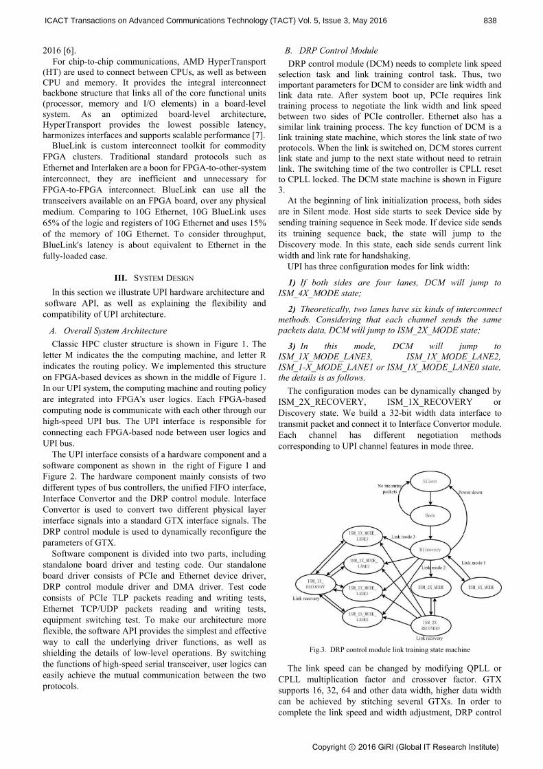
The UPI interface consists of a hardware component and asoftware component as shown in the right of Figure 1 andFigure 2. The hardware component mainly consists of twodifferent types of bus controllers, the unified FIFO interface,Interface Convertor and the DRP control module. InterfaceConvertor is used to convert two different physical layerinterface signals into a standard GTX interface signals. TheDRP control module is used to dynamically reconfigure theparameters of GTX.
Software component is divided into two parts, includingstandalone board driver and testing code. Our standaloneboard driver consists of PCIe and Ethernet device driver,DRP control module driver and DMA driver. Test codeconsists of PCIe TLP packets reading and writing tests,Ethernet TCP/UDP packets reading and writing tests,equipment switching test. To make our architecture moreflexible, the software API provides the simplest and effectiveway to call the underlying driver functions, as well asshielding the details of low-level operations. By switchingthe functions of high-speed serial transceiver, user logics caneasily achieve the mutual communication between the twoprotocols.
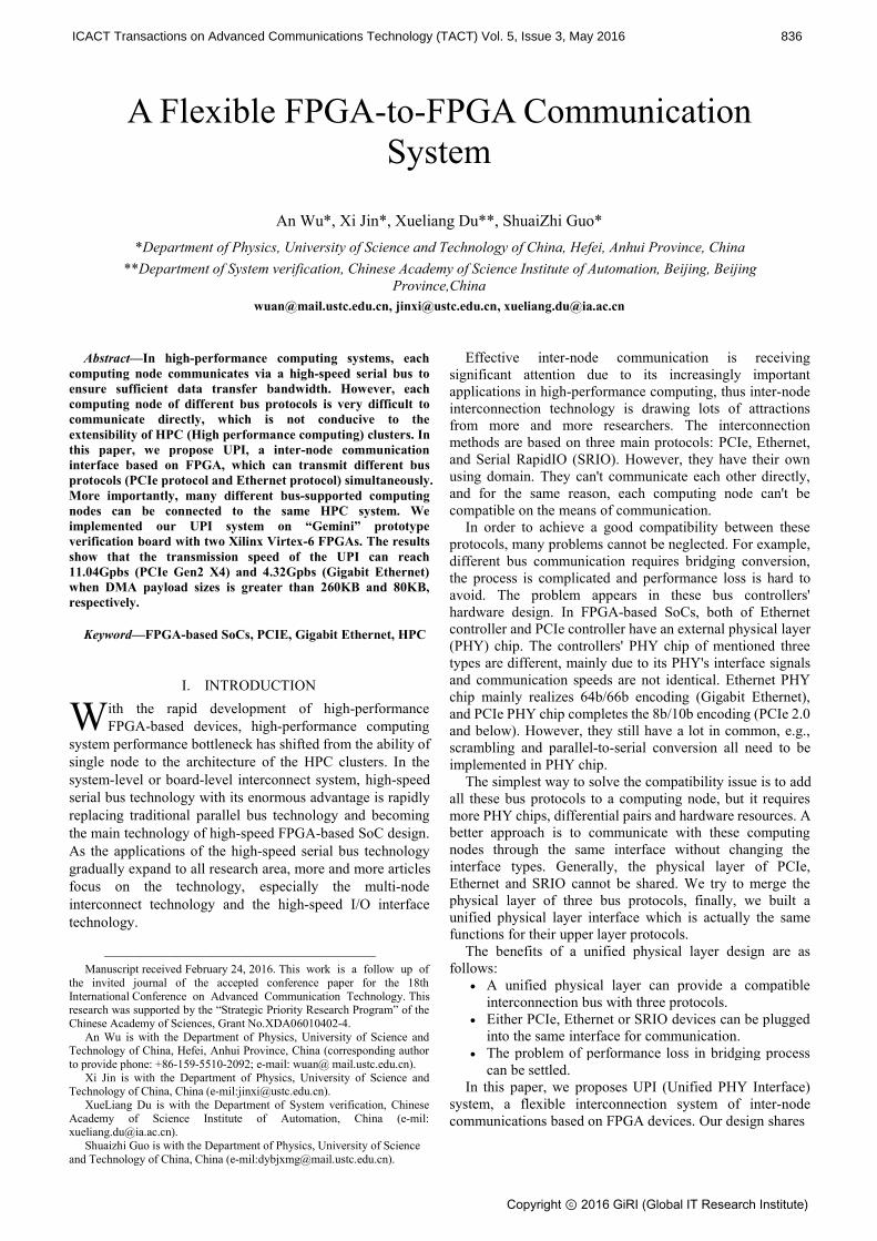
B. DRP Control ModuleDRP control module (DCM) needs to complete link speed
selection task and link training control task. Thus, twoimportant parameters for DCM to consider are link width andlink data rate. After system boot up, PCIe requires linktraining process to negotiate the link width and link speedbetween two sides of PCIe controller. Ethernet also has asimilar link training process. The key function of DCM is alink training state machine, which stores the link state of twoprotocols. When the link is switched on, DCM stores currentlink state and jump to the next state without need to retrainlink. The switching time of the two controller is CPLL resetto CPLL locked. The DCM state machine is shown in Figure3.
At the beginning of link initialization process, both sidesare in Silent mode. Host side starts to seek Device side bysending training sequence in Seek mode. If device side sendsits training sequence back, the state will jump to theDiscovery mode. In this state, each side sends current linkwidth and link rate for handshaking.
UPI has three configuration modes for link width:
1) If both sides are four lanes, DCM will jump toISM_4X_MODE state;
2) Theoretically, two lanes have six kinds of interconnectmethods. Considering that each channel sends the samepackets data, DCM will jump to ISM_2X_MODE state;
3) In this mode, DCM will jump toISM_1X_MODE_LANE3, ISM_1X_MODE_LANE2,ISM_1-X_MODE_LANE1 or ISM_1X_MODE_LANE0 state,the details is as follows.
The configuration modes can be dynamically changed byISM_2X_RECOVERY, ISM_1X_RECOVERY orDiscovery state. We build a 32-bit width data interface totransmit packet and connect it to Interface Convertor module.Each channel has different negotiation methodscorresponding to UPI channel features in mode three.
Fig.3. DRP control module link training state machine
The link speed can be changed by modifying QPLL orCPLL multiplication factor and crossover factor. GTXsupports 16, 32, 64 and other data width, higher data widthcan be achieved by stitching several GTXs. In order tocomplete the link speed and width adjustment, DRP control
ICACT Transactions on Advanced Communications Technology (TACT) Vol. 5, Issue 3, May 2016 838
Copyright ⓒ 2016 GiRI (Global IT Research Institute)
module generates different interface signals in different states.For example, when the bus controller is PCIe Gen2 X4, theCPLL reference clock can be adjusted to 125MHz, CPLLoutput rate 2.5GHz and data link width can be adjusted to 32bit data with 4bit k symbol indicator.
C. Interface ConvertorPCIe PHY interface is called PIPE interface, and Ethernet
PHY interface is called RGMII In order to achieve a mutuallycompatible interfaces, we need to make PCIe and Ethernetphysical layer interface convert to the same GTX interface.This conversion process is completed in Interface Converter.Table 1 shows the interface signals associated with the GTX,including indicators sending and receiving 32-bit words with4-bit k symbol and link status control signals.
TABLE IINTERFACE CONVERTOR RELATED SIGNAL
Signal I/O Description
GTX
mac_phy_rxdata[31:0] I receive data
mac_phy_rxdatak[3:0] I K characterindication
mac_phy_txdata[31:0] O transmit data
mac_phy_txdatak[3:0] O K characterindication
phy_mac_rxvaild[3:0] O receive data is valid
phy_mac_rxelecidle[3:0] O receive electricalidle
phy_mac_phystate[3:0] O PHY functionsmac_phy_txdetectrx_loopback[3:0] I enable receiver
detec-tion sequence
mac_phy_txelecidle[3:0] I transmit electricalidle
mac_phy_txcompliance[3:0] I Compliancesequence
macphy txpolarity[3:0] I Invert the receiveddata when asserted
mac_phy_powerdown[2:0] I PHY power down
DRP
bus_state_write[5:0] Ocurrent controllerstatewrite to DRP
bus_state_read[5:0] Icurrent controllerstateread to DRP
bus_switch_en O bus switch enablebus_link_speed[3:0] O bus link speedbus_link_width[15:0] I bus link width
The Interface Convertor mainly includes the followingfeatures:
A set of dual-port RAM, the amount of which is equalto the converted upper interfaces.
Combining and scattering data to meet UPI interfacedata width.
Generating PHY's control signals. If the control signalsprovided by GTX interface, it can be directlyconnected to GTX. Signals that GTX does not providewill be generated in Interface Converter according tothe control signals' relations or be set to a constantvalue. For example, the PCIe PIPE interface signalmac_phy_blockaligncontrol is only used in PCIe 3.0,which isn't used in our design, so we give it a constantvalue in Interface Converter.
Transmitting link information to the DCM module,completing real-time parameter changes for GTX. Thelink status signals will change into the DCM signals.
Interface Convertor signals are illustrated in Table 1.Some signals, such as clock and reset, are omitted in thistable.
D. Data structuresThere are three kinds of data structure in our UPI system:
Primary data with DMA descriptors, PCIe and Ethernetpackets data with their own protocols, GTX data with Controlsymbol. The Primary data has been stored into DDR withsome DMA descriptors. When PCIe or Ethernet controllerobtains a writing command from CPU, a segment of primarydata will be sent to the controller. PCIe controller transfersprimary data to Transaction Layer Packets(TLP). Data LinkLayer Packets(DLLP) are in charge of link maintenance. TLPpackets will be assembled with a sequence number and aLCRC code in Data Link Layer. Each TLP can accommodate4096 Bytes data payload. In Ethernet controller, relatedpackets are TCP, UDP, etc., which have 256 Byte's datapayload.
When GTX receives packets data form controllers, eachkind of packets is marked with a identifier and two kinds ofcontrol symbols (CON symbol and END symbol). Wedistinguish PCIe and Ethernet packets with binary code ''01''and ''10'', respectively. Different packets have different CONsymbol. For example, STP symbol is added to the head ofTLP packets corresponding to the identifier. The details ofCON symbols are listed in table 2. In our design, the packetswith identifier is only generated and digested in UPI layer.
TABLE IICONTROL SYMBOLS IN DCM
E. Hardware Interface and Software APIOur UPI system interface includes the following
functions: FIFO-based DMA interface. DCM interface. System interrupt interface.We use FIFO as the DMA interface for three reasons. First,
FIFO can be used between two clock domains. Our PCIesystem clock is 125MHz while Ethernet is 100MHz. Twoclock domains can be isolated by FIFO interface. Second,FIFO is a standard interface. It can shield the low-leveldetails of UPI hardware, so the transmission process in UPI istransparent for user logic. Third, the width and depth of FIFOcan be configured by circumstances of the design and it'sconvenient for developers to comprehend packet structures.FIFO-based DMA interface is used to transmit data fromsystem's memory to system's I/O controller.
The DCM interface uses a simple DCM bus to read andwrite DCM registers. We provide DCM interface to make oursystem easier to operate. For some customized HPC clusters,the DCM interface provides a function to change the busprotocol to meet developers' requirements. Through theDCM Interface, developers even can change the type ofcommunication protocol, which makes the system moreflexible of protocol switching.
System interrupt interface is a standard vectored interruptinterface. The main functions provided by the systeminterrupt interface are software interrupt generating, interrupt
Standard identifier Control symbolTLP 01 K27.7DLLP 01 K28.2TCP 10 K28.0UDP 10 K28.4
ICACT Transactions on Advanced Communications Technology (TACT) Vol. 5, Issue 3, May 2016 839
Copyright ⓒ 2016 GiRI (Global IT Research Institute)
source searching, interrupt number generating and interruptpriority setting. Different interrupt numbers mean thatdifferent interrupt exceptions and different CPU responseprocess.
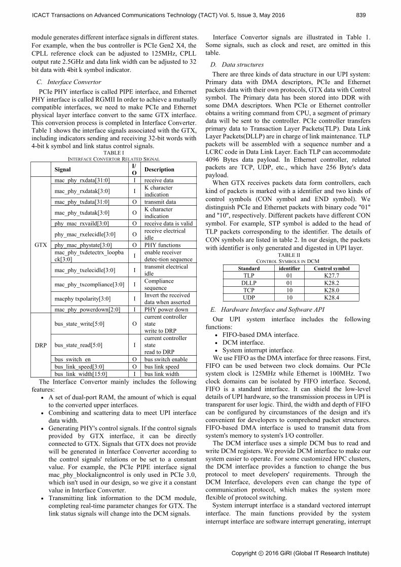
Fig.4. Structure of FPGA-based verification system
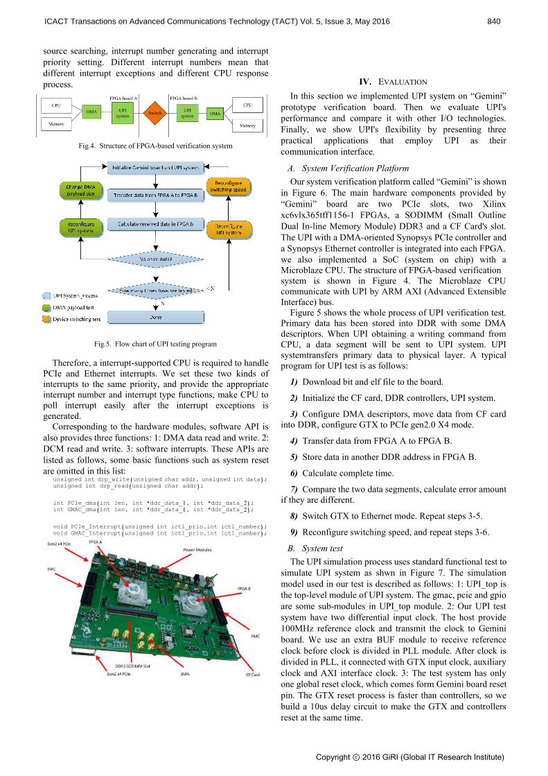
Fig.5. Flow chart of UPI testing program
Therefore, a interrupt-supported CPU is required to handlePCIe and Ethernet interrupts. We set these two kinds ofinterrupts to the same priority, and provide the appropriateinterrupt number and interrupt type functions, make CPU topoll interrupt easily after the interrupt exceptions isgenerated.
Corresponding to the hardware modules, software API isalso provides three functions: 1: DMA data read and write. 2:DCM read and write. 3: software interrupts. These APIs arelisted as follows, some basic functions such as system resetare omitted in this list:
unsigned int drp_write(unsigned char addr, unsigned int data);unsigned int drp_read(unsigned char addr);
int PCIe_dma(int len, int *ddr_data_1, int *ddr_data_2);int GMAC_dma(int len, int *ddr_data_1, int *ddr_data_2);
void PCIe_Interrupt(unsigned int ictl_prio,int ictl_number);void GMAC_Interrupt(unsigned int ictl_prio,int ictl_number);
IV. EVALUATION
In this section we implemented UPI system on “Gemini”prototype verification board. Then we evaluate UPI'sperformance and compare it with other I/O technologies.Finally, we show UPI's flexibility by presenting threepractical applications that employ UPI as theircommunication interface.
A. System Verification PlatformOur system verification platform called “Gemini” is shown
in Figure 6. The main hardware components provided by“Gemini” board are two PCIe slots, two Xilinxxc6vlx365tff1156-1 FPGAs, a SODIMM (Small OutlineDual In-line Memory Module) DDR3 and a CF Card's slot.The UPI with a DMA-oriented Synopsys PCIe controller anda Synopsys Ethernet controller is integrated into each FPGA.we also implemented a SoC (system on chip) with aMicroblaze CPU. The structure of FPGA-based verificationsystem is shown in Figure 4. The Microblaze CPUcommunicate with UPI by ARM AXI (Advanced ExtensibleInterface) bus.
Figure 5 shows the whole process of UPI verification test.Primary data has been stored into DDR with some DMAdescriptors. When UPI obtaining a writing command fromCPU, a data segment will be sent to UPI system. UPIsystemtransfers primary data to physical layer. A typicalprogram for UPI test is as follows:
1) Download bit and elf file to the board.
2) Initialize the CF card, DDR controllers, UPI system.
3) Configure DMA descriptors, move data from CF cardinto DDR, configure GTX to PCIe gen2.0 X4 mode.
4) Transfer data from FPGA A to FPGA B.
5) Store data in another DDR address in FPGA B.
6) Calculate complete time.
7) Compare the two data segments, calculate error amountif they are different.
8) Switch GTX to Ethernet mode. Repeat steps 3-5.
9) Reconfigure switching speed, and repeat steps 3-6.
B. System testThe UPI simulation process uses standard functional test to
simulate UPI system as shwn in Figure 7. The simulationmodel used in our test is described as follows: 1: UPI_top isthe top-level module of UPI system. The gmac, pcie and gpioare some sub-modules in UPI_top module. 2: Our UPI testsystem have two differential input clock. The host provide100MHz reference clock and transmit the clock to Geminiboard. We use an extra BUF module to receive referenceclock before clock is divided in PLL module. After clock isdivided in PLL, it connected with GTX input clock, auxiliaryclock and AXI interface clock. 3: The test system has onlyone global reset clock, which comes form Gemini board resetpin. The GTX reset process is faster than controllers, so webuild a 10us delay circuit to make the GTX and controllersreset at the same time.
ICACT Transactions on Advanced Communications Technology (TACT) Vol. 5, Issue 3, May 2016 840
Copyright ⓒ 2016 GiRI (Global IT Research Institute)

System test uses Vivado 14.3 ISIM simulation and VCS
Fig.7. Structure of UPI system test
2014.09-3 simulation tools to verify our design. Afterfunctional simulation pass, system test uses Synplify PremierH-2013.03 for RTL implementation and Vivado Chipscopefor testing signals observation. The simulation result isshown in Figure 7.The signal uli_lane_oe_3 available after the other threechannels' signals because of the UPI system treat lane four asa special channel. Lane four is used to send control signal andsome special communication signals.
Fig.8. UPI system simulation test
Figure 9 shows the FIFO state when UPI system starts towork.
Fig.10. DCM and Interface Convertor states of UPI system
Fig.9. FIFO state of UPI system
Using chipscope to observe the signals come form DCMand Interface convertor, we can clearly see that the currentlink is in the negotiation state before time of 124us as shownin Figure 10.
After time of 124us, DCM state machine will jump into thenext state for exchange link information and link width.
The final placement and layout of the UPI system areshown in Figure 11. Under the control of the PCIe andEthernet function can be switched by DCM. It uses fewerresources to complete switching function and improves theflexibility of UPI system. This process needs cost some extraarea. However, it would increase the system running timesignificantly for low data throughput or real timeapplications.
Fig.11. UPI system layout diagram
ICACT Transactions on Advanced Communications Technology (TACT) Vol. 5, Issue 3, May 2016 841
Copyright ⓒ 2016 GiRI (Global IT Research Institute)

The design was constrained to the right hand corner of thedevice where the PCIe and Ethernet blocks resides, as shownin Figure 2. The place with red marked is our UPI wrapper.The maximum clock rate of UPI system is limited only by thedesign, build tools, and FPGA placing and routing methods.
Fig.12. Performance of UPI system
C. Experimental ResultsMaximum data rates of PCIe and Ethernet are 20Gbps and
4Gbps, respectively. Effective data rate(MB/s) =serial busclock frequency * 1 Byte(bit/8)* number of ports * encodingformat * half-duplex/ full-duplex.
For our design, using X4 lanes, 8/10encoding, full-duplexmode and 2.5GHz(PCIe)/1.25G(GMAC) serial bus clock,effective data rate is 16Gbps/8Gpbs, i.e., 4Gpbs/2Gpbs perlane. System performance can't reach the maximum data ratebecause of some limits. The highest data rate in test is about74% of the maximum data rate, calculated from the clockfrequency of PLL.
We repeat our test more than 200 times. With the DMApayload sizes keep growing, the performance of UPI alsokeeps increasing. In DMA payload test, the data rate of bothcontrollers increases as the amount of data increase, as shownin Figure 12. When the DMA payload sizes is larger than80KB, data rate of Ethernet hold steady at 1.1Gbps while data
rate of PCIe still increasing. The data rate of PCIe becomessaturated at 2.8Gbps when payload sizes is larger than260KB. Ethernet data rate entering saturation more quicklythan PCIe because of the maximum packet sizes of Ethernet.Although the data rate of Ethernet is slower than PCIe, theEthernet physical layer uses 64b/66b encoding, makesEthernet more effective than PCIe in terms of transmissionefficiency.
TABLE IIIRESULTS OF DEVICE SWITCHING TEST
bit errorSwitching time(us) full_duplex_PCIe full_duplex_Ethernet
2.58 100% 100%1.85 92.6% 93.72%1.43 46.71% 72.7%1.04 18.5% 29.35%0.61 0.037% 0.045%
In Device switching test, we recorded the relationshipbetween bit error and switching time as shown in table 3. UPIcan normally work at 2.58us. But as the switching speedaccelerated to 1.85us, the bit error increase significantly.When the switching time is less than 500ns, no data enteredFPGA B. There are three reasons why the system appears thisphenomenon: 1) The switching time is close to the GTX'srequired reset time, when switching time is less than 500ns,GTX's CPLL is always in the unlocked state, and GTX isunable to complete the transfer task. 2) Some transferringdata are stored in FIFO, the data will be flushed after GTX'sCPLL reset. In this situation, all data already transmitted areno error. 3) High speed switching causes analog circuitscrosstalk especially differential pairs.
When the switching time is more than 2.58us, and thetransmission data is greater than 260KB, all transmitted datecan be received with no bit errors, except for the write dataerrors generated by DDR itself.
The resource consumption of UPI system is listed in table4. We also compare the performance of UPI system withother interconnect I/O technologies as shown in table 4. Theresults showed that despite the fact that our systems takemore resources, UPI system achieves a better flexibility andcompatibility. When performance and resources are able tomeet the demand of bandwidth between nodes, we madecomputing nodes of two different protocols compatible.
TABLE IVRESOURCE CONSUMPTION OVERVIEW
Resource Our Design in FPGA A Our Design in FPGA B UPI system Resource AvailableLUTs 94528(41.5%) 101064(44.4%) 11853(5.2%) 227520I/O 5(0.4%) 5(0.4%) N/A 1156
Flip-Flops 65372(14.4%) 84432(18.6%) 8224(1.8%) 455040BRAM 38(9.1%) 45(10.8%) 6(1.4%) 416
TABLE VSYSTEM PERFORMANCE OF DIFFERENT INTERCONNECT I/O TECHNOLOGIES
System Link Rate Configuration Link Rate PCI support Ethernet support LUTsBluelink[8] 10G, 40G 1x, 4x 10G No Yes 2009Infiniband[9] 40G LLC QDR 4x 10G Yes No 64105
1000 based-X Ethernet MAC 1G 1x 1.25G Yes No 11853PCIe soft IP(stratix IV) 5G 1x Gen2 5G No Yes 1805
UPI 11.04G/4.32G 1x, 2x, 3x, 4x 2.76G/1.08G Yes Yes 5500
ICACT Transactions on Advanced Communications Technology (TACT) Vol. 5, Issue 3, May 2016 842
Copyright ⓒ 2016 GiRI (Global IT Research Institute)

D. Practical Application of UPIUPI has been used in three practical applications in various
institutes. These applications include: MaPU (MathematicsProcess Unit) commodity FPGA clusters; HDR (HighDynamic Range) vedio clouding system; MOND (ModifiedNewtonian Dynamics) hardware accelerator for astronomicaldata. All these applications require real-time communicationwith multiple computing nodes. UPI can be used in theapplication of a good compatibility with the traditional singleprotocol HPC clusters, as well as adding new UPI-basedcomputing node into computing system. UPI provides abetter system compatibility and interface flexibity as shownin table 5.
V. CONCLUSIONS AND FUTURE WORK
A flexible and compatible interconnect interface has beenproposed for FPGA-based multi-node communication. Wecompleted a multi-node communication interface with thebenefits of high flexibility and good compatibility. Weimplemented our design on “Gemini” prototype verificationboard with two Xilinx Virtex-6 FPGAs. The experimentalresults show that both two bus protocols can be received andtransmitted without error when DMA payload size is greaterthan 260KB (PCIe) and 80KB (Ethernet) and switching timeis greater than 2.58us. Through the interface we can easilyconnect two different HPC clusters. The performance losscaused by traditional bridge equipment is eliminated.
ACKNOWLEDGMENT
This research is supported by the “Strategic PriorityResearch Program” of the Chinese Academy of Sciences,Grant No.XDA06010402-4.
REFERENCES
[1] Budruk, Ravi, Don Anderson, and Tom Shanley., “PCI express systemarchitecture,” Addison-Wesley Professional, 2004.
[2] Intel Corporation’s, PHY Interface for the PCI Express(TM)Architecture, Specification Version 0.5. pp. 1-15, Aug. 16, 2002.
[3] Gong, Jian, et al., “An efficient and flexible host-fpga pciecommunication library,” Field Programmable Logic and Applications(FPL), 2014 24th International Conference on. IEEE, 2014.
[4] Koch D, Beckhoff C.,“Hierarchical reconfiguration of FPGAs,” FieldProgrammable Logic and Applications (FPL), 2014 24th InternationalConference on. IEEE, 2014: 1-8.
[5] Xilinx Inc., 7 Series FPGAs GTX/GTH Transceivers User Guide, April22,2013.
[6] Islam, Nusrat S., et al.,“High performance RDMA-based design ofHDFS over InfiniBand.,” Proceedings of the International Conferenceon High Performance Computing, Networking, Storage and Analysis.IEEE Computer Society Press, 2012.
[7] Shainer, Gilad, et al.,“Maximizing application performance in amulti-core, NUMA-aware compute cluster by multi-level tuning.,”Supercom-puting. Springer Berlin Heidelberg, 2013.
[8] Theodore Markettos, “A Interconnect for commodity FPGA clusters:standardized or customized?,” Field Programmable Logic andAp-plications (FPL), 2014 24th International Conference on. IEEE,2014.
[9] TPolybus Systems Corporation, “InfiniBand cores. ,”http://www.polybus.com/iblink layer website/ibcores brochure alt.pdf
An Wu received his B.S. degree in 2011 from Schoolof Anhui University, Anhui province, China, and he iscurrently a Ph.D. student in Department of Physics inUniversity of Science and Technology of China,Anhui, China, under the supervision of Prof. Xi Jin.His current research work is mainly on SoC designtechnology, VLSI design and FPGA-based HardwareAccelerator design.
Xi Jin received the B.S. degree from University ofScience and Technology of China, Anhui, China, andhe is currently an associate professor in Department ofPhysics in University of Science and Technology ofChina, Anhui, China. His research interests includeSOC design technology, VLSI design,computer-aided design methodologies for SoC systemintegration and FPGA-based Hardware structuredesign.
Xueliang Du received the Ph.D degree fromUniversity of Science and Technology of China,Anhui, China, and he is currently an associateprofessor in Institute of Automation Chinese Academyof Sciences, Beijing, China. His research interestsinclude High-Performance SoC Design, DSP Designand FPGA-based prototyping.
Shuaizhi Guo received his B.S. degree fromUniversity of Science and Technology of China, andhe is currently a M.S. student in Department ofPhysics in University of Science and Technology ofChina, Anhui, China, under the supervision of Prof.Xi Jin. His current research work is mainly onFPGA-based Hardware Accelerator design.
ICACT Transactions on Advanced Communications Technology (TACT) Vol. 5, Issue 3, May 2016 843
Copyright ⓒ 2016 GiRI (Global IT Research Institute)


![An Efficient Key Partitioning Scheme for Heterogeneous ...icact.org/upload/2016/0211/20160211_finalpaper.pdf · large amount of data in parallel. ... File System [6], within which](https://img.pdfslide.us/doc/110x75/5b4d5f147f8b9ac9758b6fe0/an-efficient-key-partitioning-scheme-for-heterogeneous-icactorgupload2016021120160211.jpg)