Embed Size (px)
Citation preview
Semiconductor
Equipment
Assessment
SEA4KET PROJECT – BULLETIN
4 Key
Enabling
Technologies
Advances proposed in SP3
• Spin Clean Systems are being used for high
volume production in FEOL, MOL and BEOL
for 1x nm technology on 300mm wafers
• New technology nodes of 10nm and smaller
require improved control of process
parameters for critical cleans.
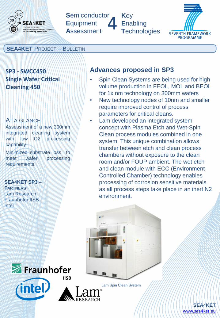
• Lam developed an integrated system
concept with Plasma Etch and Wet-Spin
Clean process modules combined in one
system. This unique combination allows
transfer between etch and clean process
chambers without exposure to the clean
room and/or FOUP ambient. The wet etch
and clean module with ECC (Environment
Controlled Chamber) technology enables
processing of corrosion sensitive materials
as all process steps take place in an inert N2
environment.
AT A GLANCE Assessment of a new 300mm
integrated cleaning system
with low O2 processing
capability.
Minimized substrate loss to
meet wafer processing
requirements.
SEA4KET www.sea4ket.eu
SEA4KET SP3 –
PARTNERS
Lam Research
Fraunhofer IISB
Intel
SP3 - SWCC450 Single Wafer Critical Cleaning 450
Lam Spin Clean System
SEA4KET PROJECT – BULLETIN
Semiconductor
Equipment
Assessment 4
Key
Enabling
Technologies
SEA4KET www.sea4ket.eu
Project Results
• Advantages of low O2 processing
to minimize CD loss demonstrated
for several FEOL applications
• New Point-Of-Use chemical mixing
provides flexible control of
process parameters directly at the
point of use on the wafer
• Particles, metal contamination and
uniformity within specification
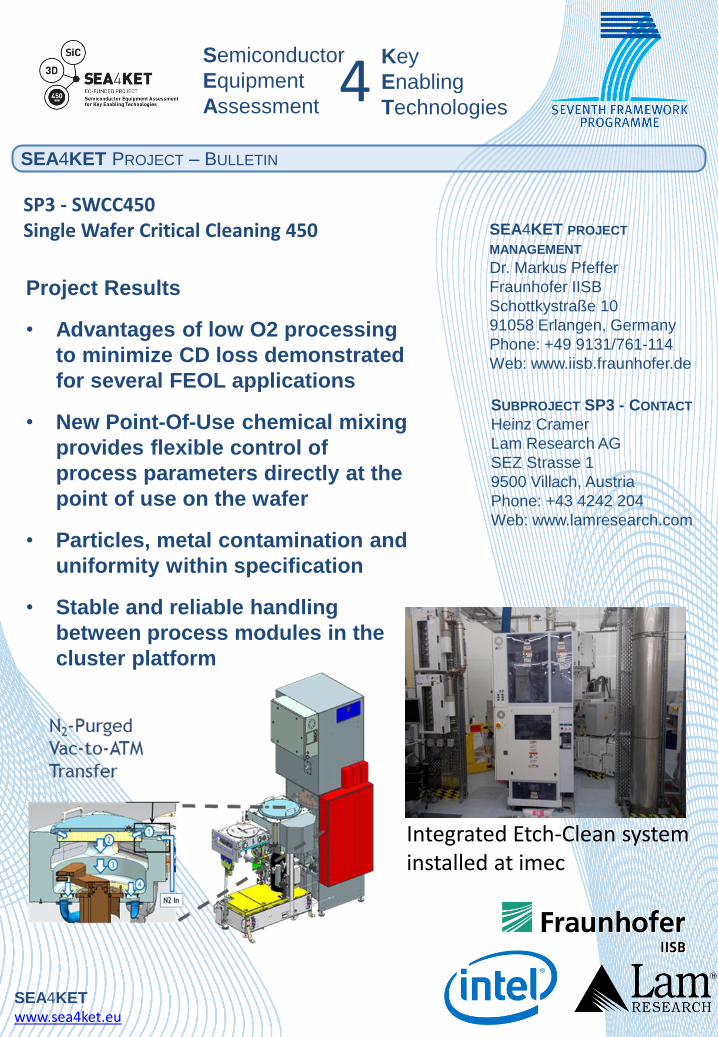
• Stable and reliable handling
between process modules in the
cluster platform
SEA4KET PROJECT
MANAGEMENT
Dr. Markus Pfeffer
Fraunhofer IISB
Schottkystraße 10
91058 Erlangen, Germany
Phone: +49 9131/761-114
Web: www.iisb.fraunhofer.de
SP3 - SWCC450 Single Wafer Critical Cleaning 450
SUBPROJECT SP3 - CONTACT
Heinz Cramer
Lam Research AG
SEZ Strasse 1
9500 Villach, Austria
Phone: +43 4242 204
Web: www.lamresearch.com
Integrated Etch-Clean system installed at imec

Semiconductor
Equipment
Assessment
SEA4KET PROJECT – BULLETIN
4 Key
Enabling
Technologies
Advances proposed in SP4
Prove general ability of 450mm Batch Oxidation System for future 450mm production requirements in G450C pilot line, with respect to process capability, repeatability, cleanliness, equipment reliability, physical tool performance and system internal contamination
Specific improvements are expected in the areas of reduction of logistics overhead time, contamination performance, efficient mini-environment purging, and isolation and uniform heat distribution of heating element and flange area.
After validation several of the expected improvements can be considered for 300mm batch equipment
AT A GLANCE
Assessment of 450mm
Batch Oxidation System
for future 450mm
production requirements
Optimization of
equipment and process
parameters to meet
wafer processing
requirements
SEA4KET www.sea4ket.eu
SEA4KET SP4 – PARTNERS
SP4: Advanced Batch
Processing
Assessment location: G450C 450mm pilotline, utilizing Equipment Performance Metrics (EPM) and Demonstration Test Methods (DTM) as agreed between G450C and European consortia
SEA4KET PROJECT – BULLETIN
Semiconductor
Equipment
Assessment 4
Key
Enabling
Technologies
SEA4KET www.sea4ket.eu
SEA4KET PROJECT
MANAGEMENT
Dr. Markus Pfeffer
Fraunhofer IISB
Schottkystraße 10
91058 Erlangen, Germany
Phone: +49 9131/761-114
Web: www.iisb.fraunhofer.de
Final process results
SUBPROJECT SP4 - CONTACT
Hessel Sprey
ASM International N.V.
PO Box 60165
1320 AE Almere
The Netherlands
Phone: +32-474-016518
Web: www.asm.com
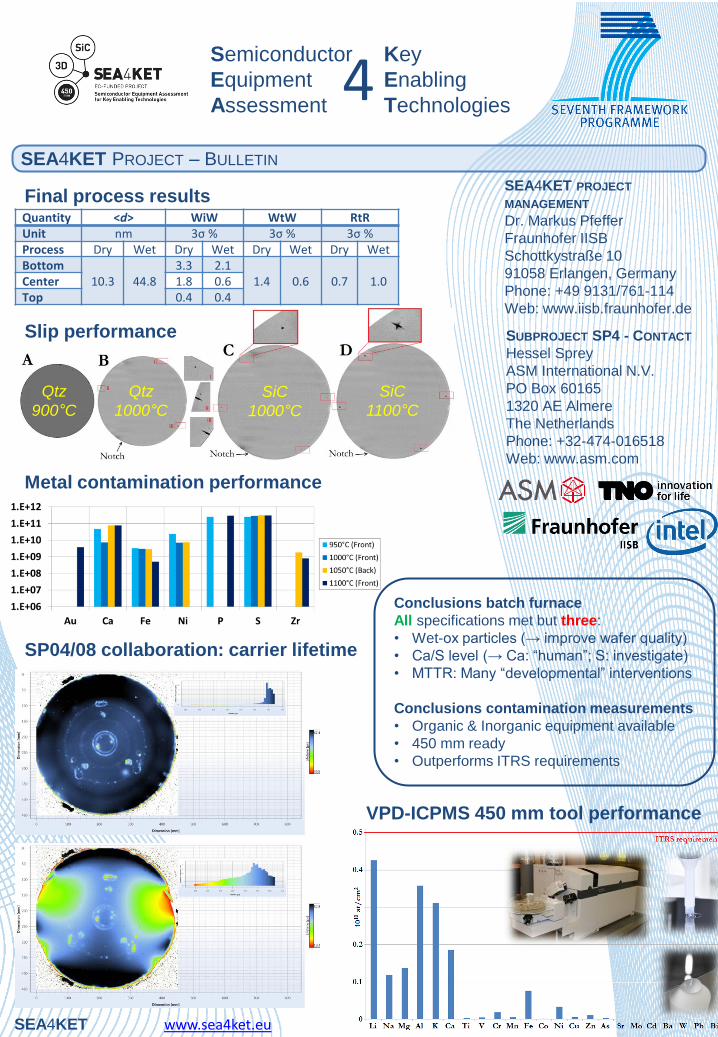
Quantity <d> WiW WtW RtR
Unit nm 3σ % 3σ % 3σ %
Process Dry Wet Dry Wet Dry Wet Dry Wet Bottom
10.3 44.8
3.3 2.1
1.4 0.6 0.7 1.0 Center 1.8 0.6
Top 0.4 0.4
Metal contamination performance
Slip performance
Qtz
900°C
Qtz
1000°C
SiC
1000°C
SiC
1100°C
VPD-ICPMS 450 mm tool performance
SP04/08 collaboration: carrier lifetime
Conclusions batch furnace
All specifications met but three:
• Wet-ox particles (→ improve wafer quality)
• Ca/S level (→ Ca: “human”; S: investigate)
• MTTR: Many “developmental” interventions
Conclusions contamination measurements
• Organic & Inorganic equipment available
• 450 mm ready
• Outperforms ITRS requirements
SEA4KET PROJECT – BULLETIN
Semiconductor
Equipment
Assessment 4
Key
Enabling
Technologies
Advances proposed in SP5
Clean and safe handling of ultra thin 300 mm
wafers and 450 mm wafers
Enabling contact free handling for 450 mm
wafers and thinned wafer substrates with
smaller wafer diameters
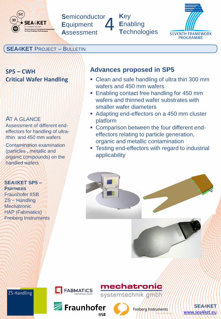
Adapting end-effectors on a 450 mm cluster
platform
Comparison between the four different end-
effectors relating to particle generation,
organic and metallic contamination
Testing end-effectors with regard to industrial
applicability
AT A GLANCE Assessment of different end-
effectors for handling of ultra-
/thin and 450 mm wafers
Contamination examination
(particles , metallic and
organic compounds) on the
handled wafers
SEA4KET www.sea4ket.eu
SEA4KET SP5 –
PARTNERS
Fraunhofer IISB
ZS – Handling
Mechatronic
HAP (Fabmatics)
Freiberg Instruments
SP5 – CWH Critical Wafer Handling
SEA4KET PROJECT – BULLETIN
Semiconductor
Equipment
Assessment 4
Key
Enabling
Technologies
SEA4KET www.sea4ket.eu
Project Results
Different handling technologies were
compared regarding:
• Particle contamination
• Organic contamination
• Metallic contamination
• Longtime tests
Established systems for measuring
organic and metallic contamination
on 450 mm wafers
SEA4KET PROJECT
MANAGEMENT
Dr. Markus Pfeffer
Fraunhofer IISB
Schottkystraße 10
91058 Erlangen, Germany
Phone: +49 9131/761-114
Web: www.iisb.fraunhofer.de
SP5 – CWH Critical Wafer Handling
SUBPROJECT SP5 - CONTACT
Clara Zängle
Fraunhofer IISB
Schottkystraße 10
91058 Erlangen, Germany
Phone: 09131-761-188
Web: www.iisb.fraunhofer.de

SEA4KET PROJECT – BULLETIN
Semiconductor
Equipment
Assessment 4
Key
Enabling
Technologies
Advances proposed in SP6
Development & manufacturing of 450mm carrier and interface
Attachment of the system to the 300/450mm cluster at FhG IISB
Assessment of the tool/process in this 300/450mm cluster platform
AT A GLANCE Assessment of vacuum
carrier technology for
handling of 300-450mm
wafers
Optimization of carrier
parameters to meet wafer
transport and storage
requirements
SEA4KET www.sea4ket.eu
SEA4KET SP6 –
PARTNERS
Fraunhofer IISB
Pfeiffer Vacuum (PV-F)
ASM
SP6- AMLL450 Vacuum transportation interface for 450mm architecture
SEA4KET PROJECT – BULLETIN
Semiconductor
Equipment
Assessment 4
Key
Enabling
Technologies
SEA4KET www.sea4ket.eu
Project Results
•Market need evaluation: R&D
• Assessment of 300 mm carrier
cleanliness by IISB, in the 300/450mm
cluster platform /
•Development of tests methodology
• Validation of cleaning process
• Study of 450mm carrier
• Material investigation
•Material assessment for future carrier
(no added contamination)
SEA4KET PROJECT
MANAGEMENT
Dr. Markus Pfeffer
Fraunhofer IISB
Schottkystraße 10
91058 Erlangen, Germany
Phone: +49 9131/761-114
Web: www.iisb.fraunhofer.de
SP6- AMLL450 Vacuum transportation interface for 450mm architecture
SUBPROJECT SP6 - CONTACT
Catherine Le Guet
Pfeiffer Vacuum SAS
98, avenue de Brogny – BP
2069
74009 Annecy Cedex –
France
Phone:+33 4 5065 7893
Web: http://www.adixen.fr/en/
450 mm plate strain 2.5mm 300 carrier vs 450 mm
300 mm attached to platform for assessment
Semiconductor
Equipment
Assessment
SEA4KET PROJECT – BULLETIN
4 Key
Enabling
Technologies
Advances proposed in SP07
An assessment of SDD EDX module integration with AMIL’s 450mm defect review tool
Establish a defectivity protocol and a baseline for imec’ s 450mm/10nm technology node pilot line
AT A GLANCE New AMIL’s SDD EDX material characterization capabilities assessment for imec’s 450mm/10nm pilot line
SEA4KET www.sea4ket.eu
SEE4KET SP07 PARTNERS AMIL FhG imec Intel
SP007 – 450DM 450mm defects metrology
SEA4KET PROJECT – BULLETIN
Semiconductor
Equipment
Assessment 4
Key
Enabling
Technologies
SEA4KET www.sea4ket.eu
Project Results
SEA4KET PROJECT MANAGEMENT Dr. Markus Pfeffer Fraunhofer IISB Schottkystraße 10 91058 Erlangen, Germany Phone: +49 9131/761-114 Web: www.iisb.fraunhofer.de
SP07 – 450DM 450mm defects metrology
SUBPROJECT SP07 - CONTACT Ilan Englard Applied Materials Israel LTD Openheimer 9 76705 Rehovot Israel Phone:+31623220600 Web:[email protected]
initial status
achieved
final ta
rget
Compe
tition
ITRS
Value
defectivity
yes 1000-2000 NAv 720 >1000
yes 7 NAv 7 15
yes 1 NAv 1 1
yes >95 NAv NAv >95
yes <5 NAv NAv <5
yes >1000 NAv NAv >1000
Semiconductor
Equipment
Assessment
SEA4KET PROJECT – BULLETIN
4 Key
Enabling
Technologies
Main achievements
An open 300/450 mm platform is now available to
support metrology companies in testing their sensors.
A sensor for carrier lifetime measurement for silicon
wafer characterization at low injection levels (high
sensitivity to below 1 x 10⁹ Fe atoms/cm³) has been
developed further.
A line-based spectroscopic ellipsometer for fast
mapping of 450 mm wafers (throughput of up to 60
wafers/hr) has been devised and built.
A topography sensor for 450 mm wafers (Makyoh-
based, field-of-view ≥ 300 mm + stitching) has been
implemented.
AT A GLANCE Availability of a flexible
platform that provides an
automated, industry
compliant environment for
metrology component
evaluation
SEA4KET www.sea4ket.eu
PARTNERS Fraunhofer IISB
Freiberg Instruments
MFA Budapest
E+H Metrology
Sub-project 8 - MetroCom
Metrology Components
See activity-related project-bulletins for the results of individual
metrology component evaluation within sub-project “MetroCom”.

SEA4KET PROJECT – BULLETIN
Semiconductor
Equipment
Assessment 4
Key
Enabling
Technologies
SEA4KET www.sea4ket.eu
Benefits
A versatile metrology module including a high-quality
3D-positioning system and a communication interface is
attached to a 300/450 mm cluster handling platform.
An automated industry compliant evaluation stand for
different metrology components is built. It meets the
specification and requirements for component testing of
industrial partners.
SMEs are enabled to test and subsequently transfer
innovative measurement technologies to the market
without prior cost and effort for automation.
Feasibility studies for various sensors are successfully
performed by using the versatile metrology module,
thus demonstrating its potential and benefit for optical
and electrical characterization of wafers up to 450 mm
diameter.
SEA4KET PROJECT
MANAGEMENT Fraunhofer IISB
Dr. Markus Pfeffer
Phone: +49 9131/761-114
Email:
Web: www.iisb.fraunhofer.de
Sub-project 8 - MetroCom
Metrology Components
METROCOM - CONTACT Fraunhofer IISB
Dr. Martin Schellenberger
Phone: +49 9131/761-222
Email:
martin.schellenberger@
iisb.fraunhofer.de
Web: www.iisb.fraunhofer.de
Figure: Open platform for metrology component evaluation that comprises a 300/450 mm
transport tool and a versatile metrology module
Semiconductor
Equipment
Assessment
SEA4KET PROJECT – BULLETIN
4 Key
Enabling
Technologies
Achievements
MDP sensor development enabling contact-less
carrier lifetime measurement of eg-Silicon up to
450 mm wafer diameter at low injection levels.
Enabling contamination monitoring and thin epitaxial
layer characterization through an increased MDP
measurement sensitivity and resolution, which excel
those of competitive measurement techniques.
Sensor inherent possibility to switch between MDP
and common µPCD measurement conditions, thus
allowing for straight comparison of respective
measurement results.
Demonstration of repeatable characterization of Si
wafers up to 450 mm diameter with respect to
Impact of different wafer annealing conditions
Detrimental effects of handling tools and wafer
support systems on electronic material
properties
Metal impurity determination
Trap density distribution
Sensor application not restricted to Silicon, but also
adaptable to wide bandgap semiconductor (esp. SiC
and GaN) characterization.
AT A GLANCE Contactless, spatially resolved
and high-sensitive detection of
electronic material properties
of 450 mm Silicon wafers by
applying carrier lifetime
measurements.
SEA4KET www.sea4ket.eu
PARTNERS
Freiberg Instruments GmbH,
Fraunhofer IISB
CONTACT
Freiberg Instruments GmbH
Dr. Kay Dornich
Dornich@
FreibergInstruments.com
www.freiberginstruments.com
Assessment of carrier
lifetime metrology
within
Sub-project 8 – MetroCom
Figure 2: Carrier lifetime map of a 450 mm Si
wafer obtained by MDP measurement Figure 1: MDPmap sensor enabling carrier lifetime
measurement of 450 mm Si wafers
Semiconductor
Equipment
Assessment
SEA4KET PROJECT – BULLETIN
4 Key
Enabling
Technologies
Achievements
MFA developed a high-speed optical mapping and
monitoring tool for 450 mm wafer diameter.
Its speed is 1800 points within 1 minute on a
450 mm wafer. Continuous measurement and
evaluation is possible.
Optical models for the measurement of lateral
homogeneity of dielectric, metal and implanted
layers were developed.
Native oxide covered 450 mm Si wafer, NiSi
covered 300 mm Si-wafers and Plasma Immersion
Ion Implanted (PIII) 300 mm Si-wafers were
successfully measured in Erlangen (IISB) in a clean-
room environment
Determine thickness with sub-nm precision.
Determine refractive indices or composition with
sub-% precision.
Application not restricted to Silicon, but also
adaptable to wide bandgap semiconductor (esp. SiC
and GaN) characterization.
AT A GLANCE Contactless, spatially
resolved, high-speed and high-
sensitive detection of thin film
properties on 450 mm Silicon
wafers by applying expanded
beam ellipsometry
measurements.
SEA4KET www.sea4ket.eu
PARTNERS
MFA, Fraunhofer IISB, IMEC
CONTACT
MFA - Research Centre for
Natural Sciences, Hungarian
Academy of Sciences
Dr. Miklós Fried
Dr. Péter Petrik
Assessment of a high-
speed optical mapping
and monitoring tool
within
Sub-project 8 – MetroCom
Figure 2: Native oxide thickness-map of
a 450 mm Si wafer
Figure 1: High-speed optical mapping and monitoring
tool for 450 mm wafer diameter

Semiconductor
Equipment
Assessment
SEA4KET PROJECT – BULLETIN
4 Key
Enabling
Technologies
Achievements
Successful set-up and performance test of a novel
topography sensor based on surface-slope
measurement
Development of related control, evaluation and
analysis software for automated and reliable
topography measurements
Quick nanotopography and global shape (bow and
warp) measurements of wafers with up to 300 mm
diameter possible within one shot
Successful demonstration of topography and
nanotopography measurements of 450 mm silicon
wafers by applying stitching procedures that are
specially adapted for this purpose
Measurement results in good agreement with state-
of-the-art equipment, but also providing additional
information
Sensor applicability not restricted to silicon wafer
technology but also applicable for the investigation
of various plain surfaces
AT A GLANCE Development of a topography
sensor for 450 mm silicon
wafers and proof of
applicability
SEA4KET www.sea4ket.eu
PARTNERS
Fraunhofer IISB,
E+H Metrology GmbH
CONTACT
Fraunhofer IISB
Dr. Martin Schellenberger
martin.schellenberger@
iisb.fraunhofer.de
www.iisb.fraunhofer.de
Feasibility study of
topography metrology
within
Sub-project 8 – MetroCom
Figure: Feasibility study of the topography sensor using the metrology module provided by the sub-project:
The measurement set-up (left) and the respective results of topography (center) and nanotopography
measurements (right) of a 450 mm double-side polished silicon wafer
Topography
sensor
Semiconductor Equipment Assessment
SEA4KET PROJECT – BULLETIN
4 KeyEnablingTechnologies
3D Integrated Measurement System
Cascade Microtech CM300full-automatic dual-configuration probe station
National Instruments PXI test instrumentation in STS hard-docking test head
Cascade Microtech Pyramid Probe® RBI advanced MEMS-type probe cards/cores
AT A GLANCEAssessment of aversatile integrated test system for 300mm wafersfor 3D stacking applications:• Probing large-array fine-pitch
micro-bumps• Automatic D2D stack testing• Probing ultra-thinned Ø300mm
wafers on tape frame
SEA4KETwww.sea4ket.eu
SEA4KET SP9 – PARTNERSCascade MicrotechimecGLOBALFOUNDRIES
SP9 – 3DIMS
SEA4KET PROJECT – BULLETIN
Semiconductor Equipment Assessment 4 Key
EnablingTechnologies
Project Results
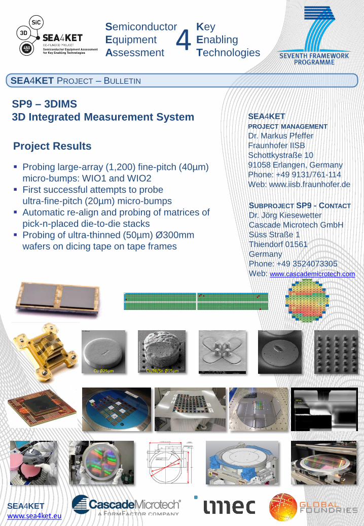
Probing large-array (1,200) fine-pitch (40µm) micro-bumps: WIO1 and WIO2
First successful attempts to probeultra-fine-pitch (20µm) micro-bumps
Automatic re-align and probing of matrices of pick-n-placed die-to-die stacks
Probing of ultra-thinned (50µm) Ø300mm wafers on dicing tape on tape frames
SEA4KETwww.sea4ket.eu
SEA4KETPROJECT MANAGEMENTDr. Markus PfefferFraunhofer IISBSchottkystraße 1091058 Erlangen, GermanyPhone: +49 9131/761-114Web: www.iisb.fraunhofer.de
SP9 – 3DIMS3D Integrated Measurement System
SUBPROJECT SP9 - CONTACTDr. Jörg KiesewetterCascade Microtech GmbHSüss Straße 1Thiendorf 01561GermanyPhone: +49 3524073305Web: www.cascademicrotech.com
Cu Ø25µm Cu/Ni/Sn Ø15µm
150 1 2 3 4 5 6 7 8 9 10 11 12 13 14 15 16 17 18 19 20 21 22 23 24 25 26 27 28 29 30 31 32 33 34 35 36 37 38 39 40 41 42 43 44 45 46 47 48 49 50 1 2 3 4 5 6 7 8 9 10 11 12 13 14 15 16 17 18 19 20 21 22 23 24 25 26 27 28 29 30 31 32 33 34 35 36 37 38 39 40 41 42 43 44 45 46 47 48 49 50
6 18.6 18.7 18.6 19.7 19.9 19.5 19.2 21.4 19.6 19.9 20.4 22.2 20.2 20.4 20.7 22.9 21.6 20.8 22.9 23.5 21.3 23.6 22.9 24.1 21.9 23.4 24.7 23.0 24.2 23.6 22.5 21.7 23.4 22.0 22.2 22.3 24.9 21.7 22.4 22.7 24.5 22.0 21.9 21.5 21.3 21.8 21.9 21.3 20.5 19.8 19.7 21.6 NaN 22.3 21.7 21.4 22.6 22.3 21.7 22.3 22.2 23.1 22.8 22.9 22.2 23.4 23.1 22.9 22.5 23.5 23.9 23.5 23.6 23.1 19.2 18.5 18.7 19.1 18.9 18.9 18.8 18.8 18.6 18.3 18.5 18.2 17.7 17.4 17.5 17.3 16.8 17.4 16.7 17.3 16.0 16.5 16.7 16.6 16.5 15.5
5 18.7 18.9 19.0 19.8 19.2 19.2 21.6 19.5 19.0 20.0 22.2 20.1 19.6 20.2 22.9 20.9 20.1 22.3 23.1 20.9 24.2 24.0 23.4 21.3 23.5 23.8 22.2 24.6 23.4 24.0 22.7 24.0 23.5 21.9 21.8 24.1 21.5 21.8 21.7 24.1 21.5 21.0 21.3 23.3 22.3 22.0 22.1 21.4 21.5 19.9 20.0 NaN 21.2 23.5 NaN 22.2 21.6 23.0 22.3 22.1 22.7 22.6 22.6 23.2 23.2 22.8 22.6 23.2 23.0 23.0 23.6 23.3 23.6 22.8 23.4 19.1 18.3 19.4 18.3 18.9 19.2 19.2 18.9 18.5 17.4 17.8 17.7 18.1 16.9 17.5 17.6 16.8 16.4 NaN 16.7 16.6 16.9 17.3 16.7 15.9
4 18.3 18.5 19.1 19.1 19.0 19.8 19.6 19.6 20.0 22.0 19.6 19.7 20.5 22.4 20.1 21.0 20.5 24.1 20.7 21.9 23.5 23.0 22.1 23.5 23.1 22.1 24.4 23.7 24.4 22.8 23.9 23.5 21.7 22.3 23.8 21.4 22.9 22.2 24.8 22.3 22.2 22.0 23.5 22.1 21.3 22.4 21.9 21.9 22.6 20.0 20.5 23.4 23.1 21.9 23.0 23.1 23.1 22.3 22.7 22.8 22.8 23.1 23.1 22.4 23.8 23.4 23.8 23.2 23.6 23.1 23.4 23.1 20.0 24.3 23.5 19.6 19.5 19.4 19.2 18.1 18.1 18.8 18.7 19.0 18.0 18.3 18.0 17.3 17.3 17.3 18.2 17.1 NaN 16.5 17.3 17.0 16.9 16.1 17.3 15.9
3 18.9 19.1 18.9 19.7 19.8 19.3 19.1 19.6 19.2 19.9 20.3 19.8 20.1 21.0 20.3 20.0 20.8 23.6 20.8 21.4 21.7 24.0 21.7 22.5 22.0 22.2 22.9 24.5 23.4 22.0 22.0 24.6 22.3 22.7 22.5 22.8 21.8 22.5 22.2 23.0 22.3 22.5 21.6 21.9 22.2 22.3 21.7 21.9 21.4 20.7 21.2 22.0 22.1 23.1 22.1 23.1 22.9 22.9 23.1 23.0 23.1 23.4 23.8 23.1 23.1 23.7 24.5 23.0 23.1 23.9 23.9 23.5 24.2 23.8 24.2 19.5 19.6 19.5 19.2 19.4 18.9 18.7 18.6 18.2 18.0 17.6 17.8 17.8 17.9 18.4 17.9 17.5 16.8 17.2 17.3 17.0 16.0 17.2 17.4 16.6
2 NaN 18.7 19.6 19.8 19.0 19.6 19.5 19.3 20.0 20.2 19.8 19.7 20.3 20.3 21.1 20.9 21.5 20.6 23.5 21.9 21.4 21.6 23.9 22.4 22.2 22.8 23.1 22.7 25.0 22.7 22.3 22.3 24.8 21.9 22.3 21.4 22.0 22.4 21.9 22.0 22.2 21.6 22.5 22.0 22.0 22.2 21.7 22.5 21.7 21.2 21.1 22.0 22.5 22.7 23.1 23.0 22.2 22.5 22.3 23.3 23.1 22.5 23.0 23.1 22.8 23.5 23.4 23.4 23.2 23.9 23.6 23.9 23.2 23.9 23.8 19.4 19.4 19.6 19.7 18.5 18.8 19.4 18.8 18.7 18.6 17.9 17.3 18.1 17.7 17.6 17.6 18.4 17.1 18.2 17.5 16.8 16.4 18.0 16.1 16.8
1 19.3 19.0 19.5 19.7 20.0 19.5 19.5 19.8 20.1 19.6 19.9 20.0 19.9 20.7 20.8 21.3 20.7 21.0 21.7 23.7 21.5 21.3 21.7 23.8 22.2 24.6 22.4 22.8 22.8 24.3 22.5 22.7 22.4 23.2 23.7 21.9 22.0 22.4 22.1 21.2 21.8 21.9 21.8 22.6 21.9 22.0 21.9 22.7 20.3 20.4 20.1 22.0 23.5 23.1 22.9 23.8 22.7 22.3 22.3 22.8 22.3 22.7 22.6 22.8 23.9 23.4 23.5 22.8 23.1 23.6 22.8 24.0 23.2 23.4 23.9 19.6 19.8 19.4 19.2 19.3 18.3 18.8 19.0 18.9 18.4 18.7 17.9 18.1 17.5 17.4 17.3 17.0 17.0 17.1 17.2 17.0 17.5 17.0 17.2 16.6
6 18.1 19.0 18.9 19.2 22.8 19.0 18.8 18.6 19.1 18.9 19.4 19.7 19.9 20.1 20.1 20.2 20.6 20.8 20.9 20.8 21.4 21.4 21.8 21.9 21.9 21.6 21.1 20.8 21.3 20.2 21.2 21.3 21.3 20.8 20.8 21.2 20.3 20.9 20.7 20.2 20.5 20.1 20.4 20.4 20.7 20.6 21.0 20.3 19.5 17.9 19.0 18.7 20.0 19.7 19.3 20.0 20.5 20.1 19.3 19.3 19.9 20.5 19.3 19.7 19.9 21.2 21.0 20.4 20.8 20.5 25.7 21.1 21.1 20.4 26.3 20.0 23.8 20.0 20.0 19.8 24.3 19.6 19.1 19.0 19.8 18.6 18.7 18.6 17.8 18.0 17.8 18.3 17.8 17.9 17.5 17.7 17.4 17.4 17.5 16.9
5 19.7 17.9 19.4 18.2 18.5 18.9 19.3 18.7 19.5 19.1 19.3 19.8 19.6 19.6 19.5 20.4 20.5 20.4 20.9 20.4 20.4 21.6 21.9 21.5 21.7 21.3 21.6 20.9 21.5 21.0 21.3 20.9 20.8 20.7 20.2 20.8 20.2 20.1 20.1 20.4 20.6 19.9 20.3 19.5 20.8 20.3 20.3 20.0 19.8 18.7 18.6 19.4 20.8 19.4 19.8 20.0 20.6 19.7 19.6 20.3 19.9 19.8 19.6 20.2 19.8 19.7 20.1 24.8 20.1 20.6 20.6 24.9 20.4 21.1 20.6 20.5 20.2 23.4 19.8 20.3 19.6 23.4 18.9 19.6 18.7 19.4 18.3 18.4 18.1 18.0 18.7 18.0 17.4 17.5 17.2 17.2 17.7 18.0 17.1 16.5
4 18.5 19.3 18.8 18.0 18.6 19.1 19.0 18.5 18.8 19.0 19.4 19.7 19.2 19.6 19.7 19.7 19.9 20.6 20.6 21.1 21.3 21.3 21.4 21.8 21.7 21.8 21.6 21.5 21.4 21.0 21.3 20.9 20.3 21.4 21.2 20.5 20.4 20.7 20.1 20.6 21.5 20.6 20.0 20.5 20.3 19.7 20.3 20.5 19.7 18.6 18.5 19.3 19.6 19.9 20.3 20.6 19.3 19.9 20.6 19.9 20.2 20.2 20.5 20.2 20.7 20.4 20.8 20.3 25.3 20.1 20.0 21.2 24.9 20.5 21.4 20.2 20.7 19.9 24.1 19.9 20.2 19.1 24.8 19.1 18.2 18.7 19.1 18.1 17.9 18.5 18.1 18.0 17.9 17.3 17.5 17.6 17.5 17.0 17.5 17.2
3 18.1 18.8 18.0 19.0 19.2 19.5 18.4 18.8 18.9 19.6 18.9 18.7 19.3 19.6 19.6 19.6 19.5 20.3 20.7 20.2 20.4 21.8 21.4 21.0 21.5 20.6 21.5 20.8 20.5 20.8 21.0 20.8 20.4 21.6 20.5 20.2 20.0 20.5 20.2 20.5 20.5 20.0 20.2 19.2 19.7 20.1 19.2 19.7 19.7 18.1 18.1 20.1 20.0 20.0 20.2 19.3 19.6 25.0 20.0 20.6 19.8 25.1 20.2 20.0 24.5 25.5 20.6 19.9 24.6 24.1 21.6 25.2 25.4 24.3 20.4 24.5 25.4 19.6 24.3 24.1 20.1 19.1 24.2 23.3 18.7 18.3 22.7 23.5 17.4 17.8 21.7 17.8 18.0 17.5 18.0 17.7 17.2 16.3 16.6 16.8
2 18.3 19.2 19.9 18.8 18.6 19.2 20.0 18.3 18.6 19.0 19.7 18.7 19.3 19.5 19.7 19.3 19.9 20.5 20.8 21.3 21.0 21.0 21.9 20.3 21.4 20.7 21.0 21.9 21.0 20.9 20.3 20.6 20.8 20.1 20.7 21.0 19.9 21.0 20.2 20.6 19.6 20.1 20.2 19.9 20.3 19.7 20.4 19.9 19.6 17.9 17.6 19.7 19.6 20.1 19.7 19.4 24.1 20.0 19.8 19.6 24.3 20.3 20.0 24.9 25.6 19.8 20.5 25.5 25.0 20.5 24.8 25.4 23.7 19.8 24.6 24.8 19.5 23.8 24.3 23.4 19.4 23.8 24.1 18.8 18.6 23.0 22.5 18.0 18.6 22.0 18.6 17.3 18.5 22.4 17.5 17.0 18.0 17.0 16.9 16.4
1 17.9 19.3 18.8 18.6 18.7 17.9 18.2 19.3 18.8 18.6 19.2 19.7 18.9 19.3 19.1 19.8 20.0 19.8 20.4 19.8 21.3 20.8 20.7 20.8 21.1 20.2 20.7 20.8 21.4 20.5 20.8 20.1 20.6 20.5 20.6 19.6 19.8 20.8 20.6 19.4 19.8 20.6 20.0 20.2 19.5 19.3 20.1 19.2 19.2 18.1 17.8 18.5 18.9 19.6 18.8 19.2 19.5 19.7 19.4 24.4 19.7 20.4 24.6 24.4 19.9 20.1 24.6 24.1 20.3 20.9 24.0 23.8 20.9 24.9 24.2 19.8 24.0 24.2 24.0 19.6 23.3 23.3 18.8 19.1 23.5 22.8 18.7 18.4 22.9 17.6 18.1 17.4 22.1 17.2 NaN 17.3 17.4 16.8 16.9 16.1
Semiconductor
Equipment
Assessment
SEA4KET PROJECT – BULLETIN
4 Key
Enabling
Technologies
Advances proposed in SP10
Development of a surface preparation method
for enabling room temperature covalent
bonding.
Characterization of the process for various
combinations of materials/surface qualities
Implementation of the newly-developed
equipment and processes into volume
manufacturing environment.
AT A GLANCE Assessment of room
temperature covalent wafer
bonding technology.
SEA4KET www.sea4ket.eu
SEA4KET SP10 –
PARTNERS
EVG
CEA LETI
ST Microelectronics
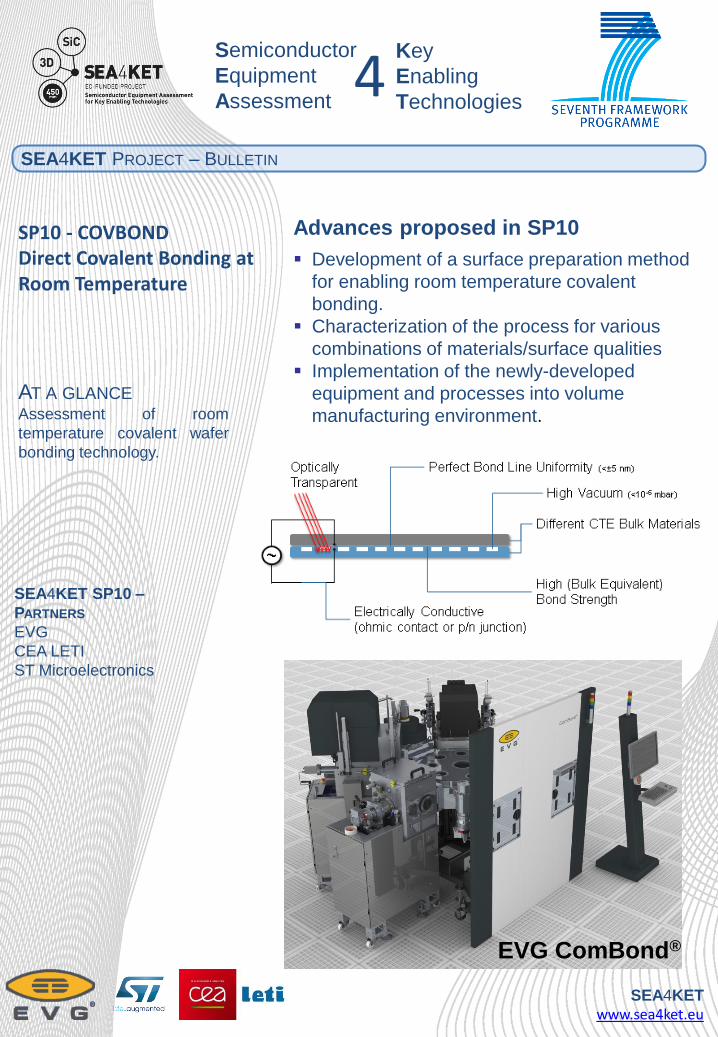
SP10 - COVBOND Direct Covalent Bonding at Room Temperature
EVG ComBond®
SEA4KET PROJECT – BULLETIN
Semiconductor
Equipment
Assessment 4
Key
Enabling
Technologies
SEA4KET www.sea4ket.eu
Project Results
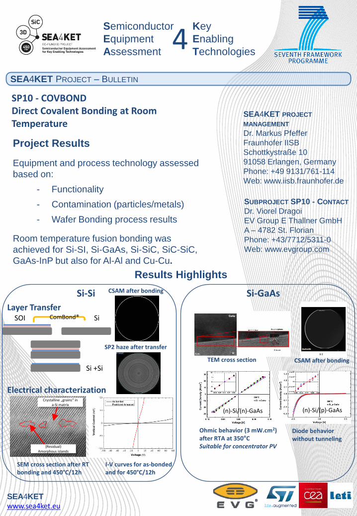
Equipment and process technology assessed
based on:
- Functionality
- Contamination (particles/metals)
- Wafer Bonding process results
Room temperature fusion bonding was
achieved for Si-SI, Si-GaAs, Si-SiC, SiC-SiC,
GaAs-InP but also for Al-Al and Cu-Cu.
SEA4KET PROJECT
MANAGEMENT
Dr. Markus Pfeffer
Fraunhofer IISB
Schottkystraße 10
91058 Erlangen, Germany
Phone: +49 9131/761-114
Web: www.iisb.fraunhofer.de
SP10 - COVBOND Direct Covalent Bonding at Room Temperature
SUBPROJECT SP10 - CONTACT
Dr. Viorel Dragoi
EV Group E Thallner GmbH
A – 4782 St. Florian
Phone: +43/7712/5311-0
Web: www.evgroup.com
Si-Si Si-GaAs
ComBond®
Layer Transfer
CSAM after bonding
SP2 haze after transfer
Electrical characterization
(Residual) Amorphous islands
Crystalline „grains“ in a-Si matrix
SEM cross section after RT bonding and 450°C/12h
I-V curves for as-bonded and for 450°C/12h
SOI Si
Si +Si CSAM after bonding TEM cross section
Ohmic behavior (3 mW.cm2) after RTA at 350°C Suitable for concentrator PV
Diode behavior without tunneling
(n)-Si/(n)-GaAs (n)-Si/(p)-GaAs
Results Highlights
Semiconductor
Equipment
Assessment
SEA4KET PROJECT – BULLETIN
4 Key
Enabling
Technologies
Advances proposed in SP11
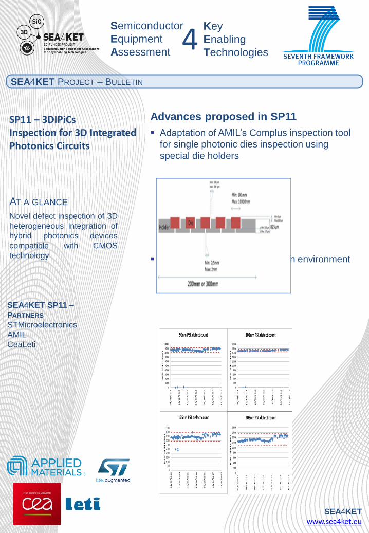
Adaptation of AMIL’s Complus inspection tool
for single photonic dies inspection using
special die holders
Inspection stability in production environment
qualifications
AT A GLANCE
Novel defect inspection of 3D
heterogeneous integration of
hybrid photonics devices
compatible with CMOS
technology
SEA4KET www.sea4ket.eu
SEA4KET SP11 –
PARTNERS
STMicroelectronics
AMIL
CeaLeti
SP11 – 3DIPiCs Inspection for 3D Integrated Photonics Circuits
X

SEA4KET PROJECT – BULLETIN
Semiconductor
Equipment
Assessment 4
Key
Enabling
Technologies
SEA4KET www.sea4ket.eu
SEA4KET PROJECT
MANAGEMENT
Dr. Markus Pfeffer
Fraunhofer IISB
Schottkystraße 10
91058 Erlangen, Germany
Phone: +49 9131/761-114
Web: www.iisb.fraunhofer.de
SP11 – 3DIPiCs Inspection for 3D Integrated Photonics Circuits
SUBPROJECT SP11 - CONTACT
Ilan Englard
Applied Materials Israel LTD
Openheimer 9
76705 Rehovot
Israel
Phone:
Web:
initial status
achieved
final target
Analysis Metrology
Measurment application (e. g. sheet resistance …) Defectivity Defectivity
Wafer type (n, p, patterned, unpatterned, pn
junction)
Patterned, unpatterned
and stickers
Demonstrated on unpatterned
stickers, on going on patterned
stickersPatterned, unpatterned
and stickers
Measurment type (Non-Contacting, Non-destructive,
contacting, destcructive)
Non contact, non
destructiveachieved
Non contact, non
destructive
Wafer preparation NA NA
Wafer postprocessing (possible, cleaning needed …) No No
Measuring Time
Time for evaluation of raw measurement
Measurement speed (Seconds/point)
Measurement Range 0 - 50 000 defects 0-100 000 defects demonstrated 0 - 50 000 defects
Detectable species (what is actually measured) Particles, holes, … All defect types captured Particles, holes, …
Sensitivity
Please see sensitivity
table below
Precision / Accuracy
"+/- 4um for GF30 and
above (per AMAT ATP)
+/- 4um for GF30 achieved
Detection Limit PSL 0,09µm Demonstrated with PSL spheres PSL 0,09µm
Repeatability
>97% on OTW and
>95% on product wafer
(by defect count only)
Achieved
Reproducibility
>97% on OTW and
>95% on product wafer
(by defect count only)
Achieved
Wafer Map Resolution NA
Wafer Map Edge Exclusion 3 mm Achieved 3 mm
Spot/measurment point size
Depends on the
magnification used.
Removal of material (etch/sputter rate; unifomity) NA NA
Equipment special feature (uniqueness …) NA NA

Semiconductor
Equipment
Assessment
SEA4KET PROJECT – BULLETIN
4 Key
Enabling
Technologies
Advances proposed in SP12
• Availability of high brightness X-ray sources
which will result in an improvement in
throughput of a factor of ~ 10.
• Improved usability and algorithms targeted
to advanced materials, photonics, and their
heterogeneous integration
• Complete prototype
• Improved analytical software for HRXRD
AT A GLANCE Assessment of X-ray
metrology on thin to ultrathin
films and on small
measurements spots
SEA4KET www.sea4ket.eu
SEA4KET SP12 –
PARTNERS
Bruker
STMicroelectronics
CEA-Leti
SP12 - XMeCK X-ray Metrology

SEA4KET PROJECT – BULLETIN
Semiconductor
Equipment
Assessment 4
Key
Enabling
Technologies
SEA4KET www.sea4ket.eu
Project Results
D8 Fabline automated diffractometer
The D8 Fabline is a highly versatile automated diffractometer for 300 mm wafers, with snap lock optics and automatic recognition of components. It was installed and accepted at CEA-LETI starting from Mar 2015. The tool is in a so called D8 Fabline-HR configuration, for HRXRD, XRR and GIXRD measurements. The tool has been used for measurements on a range of different samples of interest to CEA-Leti and therefore also representative of the interest of the broad semiconductor industry.
Strain in SiGe in small metrology pads
Patterned samples with SiGe finFET in small metrology pads have successfully been measured in Bruker Karlsruhe on the D8 Fabline-MH tool using a High Brilliance rotating anode (Turbo X-ray Source) with a 100x100µm² spot size as shown in Fig. 2. Typical measurement times are minutes per site. Capability to measure in small spots at high throughput is an enabler for further adoption of X-ray metrology in the semiconductor high volume manufacturing.
SEA4KET PROJECT
MANAGEMENT
Dr. Markus Pfeffer
Fraunhofer IISB
Schottkystraße 10
91058 Erlangen, Germany
Phone: +49 9131/761-114
Web: www.iisb.fraunhofer.de
SP12 - XMeCK X-ray Metrology
SUBPROJECT SP12 - CONTACT
Juliette Vandermeer
Bruker AXS GmbH
Rheinbruckenstrasse 49
76187 Karlsruhe
Phone: +49 721 509975620
Web: www.bruker.com
Fig. 1 D8 Fabline tool Fig. 2 An RSM on the 113 asymmetrical reflection of a small finFET pad, showing starting relaxation of the epitaxial layer

SEA4KET PROJECT – BULLETIN
Semiconductor
Equipment
Assessment 4
Key
Enabling
Technologies
SEA4KET www.sea4ket.eu
Project Results
Strain and concentration in III-V materials for
photonics and power devices
A range of III-V materials find applications in photonics and power devices. Gallium arsenide has a wider bandgap than silicon. It is therefore used in LEDs, for its efficient light emission. To the same family belong InGaAs and AlGaAs. (Al)GaN and (Al)InN are typically used in power devices. Its bandgap can be tailored as a function of the aluminium concentration in the alloy. The strain and concentrations in these alloys are important parameters for the product quality and can be determined by the D8 Fabline in HRXRD analysis mode as shown in Fig. 3.
Thickness and crystallinity of ultrathin films
Titanium nitride (TiN) films are used as diffusion barrier layers in microelectronic devices. The performance and stability of such barrier is related to the crystallinity and grain size in the film. Thin polycrystalline TiN samples of 7 nm and 3 nm were measured using XRR to analyze thickness and roughness (Fig. 4). GIXRD was used to analyze the crystalline phase (Fig. 5).
SEA4KET PROJECT
MANAGEMENT
Dr. Markus Pfeffer
Fraunhofer IISB
Schottkystraße 10
91058 Erlangen, Germany
Phone: +49 9131/761-114
Web: www.iisb.fraunhofer.de
SP12 - XMeCK X-ray Metrology
SUBPROJECT SP12 - CONTACT
Juliette Vandermeer
Bruker AXS GmbH
Rheinbruckenstrasse 49
76187 Karlsruhe
Phone: +49 721 509975620
Web: www.bruker.com
10 nm TiN
7 nm TiN
5 nm TiN
3 nm TiN
Fig. 5 The peaks at 43° and 62° that are typical for TiN are present in the 7 nm and 5 nm sample, but have disappeared in the 3 nm sample.
Fig. 4 XRR scan of 5nm TiN sample.
Fig. 3 RSM of 224 Bragg reflection; the position of InGaAs and InP is a measure for the relaxation.
Semiconductor
Equipment
Assessment
SEA4KET PROJECT – BULLETIN
4 Key
Enabling
Technologies
Advances proposed in SP13 - REPSIC
Proposed concept uses a new electron
charge driven method for enhanced oxidation
rate of SiC without oxide damage.
Process has been demonstrated on Si wafers
and SiC samples before
Remarkable reduction of oxidation
temperature and thermal budget by 500 °C
Oxide growth independent from crystal
orientation (now oxidation anisotropy)
Concept enables free combination
and sequence of oxidation and
nitridation in order to establish user
defined nitrogen profiles
New methodology to influence the
SiC-oxide interface, including its
electrical characeristics
AT A GLANCE Assessment of plasma
oxidation and nitridation tool
for SiC gate oxide formation
Optimization of chamber and
process parameters to
optimize oxide quality on SiC
SEA4KET www.sea4ket.eu
SEA4KET SP13 –
PARTNERS
Fraunhofer IISB
HQ – Dielectrics
Infineon Technologies
SP13 - REPSiC Rapid Electrical Field Driven Processing of Gate Dielectrics on Silicon Carbide
Schematic of the high-density microwave plasma
oxidation and in-situ post plasma anneal
apparatus
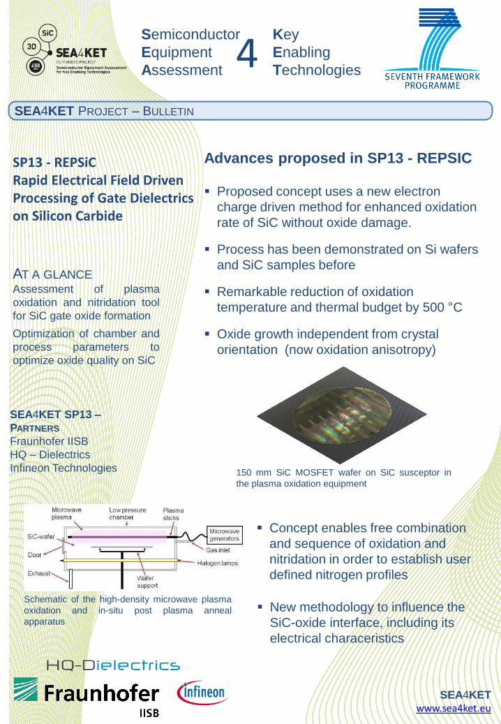
150 mm SiC MOSFET wafer on SiC susceptor in
the plasma oxidation equipment

SEA4KET PROJECT – BULLETIN
Semiconductor
Equipment
Assessment 4 Key
Enabling
Technologies
SEA4KET www.sea4ket.eu
Project Results
Multiplied oxide growth rate on SiC at
low temperature (< 1000 °C)
Excellent conformality of oxide
growth, i.e. very little anisotropy
Oxide thickness > 10 nm
demonstrated, potentially up to 20 nm
MOSCAP and MOSFET Device grown
with plasma oxide base gate dielectric
Promising first electrical results
SEA4KET PROJECT
MANAGEMENT
Dr. Markus Pfeffer
Fraunhofer IISB
Schottkystraße 10
91058 Erlangen, Germany
Phone: +49 9131/761-114
Web: www.iisb.fraunhofer.de
SP13 - REPSiC Rapid Electrical Field Driven Processing of Gate Dielectrics on Silicon Carbide
SUBPROJECT SP13 - CONTACT
Juergen Niess
HQ – Dielectrics GmbH
Dornstadter Weg 9/1
89160 Dornstadt
Phone: :+49 7348 204 825
Web www.hq-dielectrics.eu
Oxide growth rate on SiC compared to Si:
0.9 nm/min @ RT/350 ºC, 9 nm/min @ 750 ºC
Break down field satifies technological requirements
Semiconductor
Equipment
Assessment
SEA4KET PROJECT – BULLETIN
4 Key
Enabling
Technologies
Advances achieved in SP14 – TLS4SiC
Assessment of the kerf free dicing technology for
Silicon Carbide product wafers with regard to
throughput, reliability, edge quality and electrical
characteristics of separated chips and handling
issues.
Increased feed rate up to a factor of 100
compared to state of the art dicing technology.
Very high edge quality – no chipping, smooth
side walls and no delamination of backside metal
– leads to good electrical characteristic and
promises long-term stability of separated chips.
High throughput and no tool wear results in a
significantly reduction of process costs compared
with state of the art dicing technology.
TLS4SiC will be an enabler for SiC volume
production by providing a separation technology
allowing for high quality results with high
throughput far beyond state of the art.
AT A GLANCE
Assessment of an innovative
dicing technology able to
fulfill the requirements of SiC
volume production.
SEA4KET www.sea4ket.eu
SEA4KET SP14 –
PARTNERS
Fraunhofer IISB
Fraunhofer CSP
3D-Micromac AG
Infineon Technologies
SP14 – TLS4SiC
Thermal Laser Separation
for Fast High Quality
Silicon Carbide Dicing
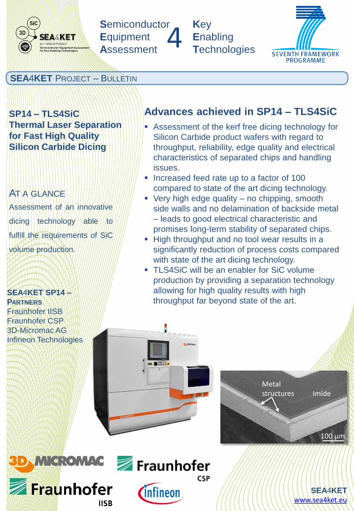
100 µm
Imide Metal structures

SEA4KET PROJECT – BULLETIN
Semiconductor
Equipment
Assessment 4 Key
Enabling
Technologies
SEA4KET www.sea4ket.eu
Project Results
Tape assessment prove that a standard dicing tape
for blade dicing can be used for TLS-DicingTM.
Developed shipping strategy for zero kerf diced
wafers guarantees damage free transportation.
Development of a process simulation model.
Successful dicing of up to 150 mm SiC diode wafers
with chips sizes down to 0.96 mm2 demonstrated.
SEM and TEM measurements proofed high chip
sidewall quality with no micro cracks.
TLS diced wafers assembled using Infineon’s
production lines in Malaysia.
Electrical measurements proof good die attach, good
electrical characteristics and long term stability of
TLS diced chips.
Next generation TLS-DicingTM tool
microDICETM developed and built up.
SEA4KET PROJECT
MANAGEMENT
Dr. Markus Pfeffer
Fraunhofer IISB
Schottkystraße 10
91058 Erlangen, Germany
Phone: +49 9131/761-114
Web: www.iisb.fraunhofer.de
SP14 – TLS4SiC
Thermal Laser Separation for Fast High
Quality Silicon Carbide Dicing
SUBPROJECT SP14 - CONTACT
Dr. Martin Schellenberger
Fraunhofer IISB
Schottkystraße 10
91058 Erlangen, Germany
Phone: +49 9131/761-222
Web: www.iisb.fraunhofer.de
x Spec. value at 1200V: 9µA