Embed Size (px)
Citation preview
Chapter 7
Advances in Resistive Switching Memories Based onGraphene Oxide
Fei Zhuge, Bing Fu and Hongtao Cao
Additional information is available at the end of the chapter
http://dx.doi.org/10.5772/51260
1. Introduction
Memory devices are a prerequisite for today’s information technology. In general, two dif‐ferent segments can be distinguished. Random access type memories are based on semicon‐ductor technology. These can be divided into static random access memories (SRAM) anddynamic random access memories (DRAM). In the following, only DRAM will be consid‐ered, because it is the main RAM technology for standalone memory products. Mass storagedevices are traditionally based on magnetic- and optical storage. But also here semiconduc‐tor memories are gaining market share. The importance of semiconductor memories is con‐sequently increasing (Mikolajick et al., 2009). Though SRAM and DRAM are very fast, bothof them are volatile, which is a huge disadvantage, costing energy and additional peripherycircuitry. Si-based Flash memory devices represent the most prominent nonvolatile datamemory (NVM) because of their high density and low fabrication costs. However, Flash suf‐fers from low endurance, low write speed, and high voltages required for the write opera‐tions. In addition, further scaling, i.e., a continuation in increasing the density of Flash isexpected to run into physical limits in the near future. Ferroelectric random access memory(FeRAM) and magnetoresistive random access memory (MRAM) cover niche markets forspecial applications. One reason among several others is that FeRAM as well as convention‐al MRAM exhibit technological and inherent problems in the scalability, i.e., in achieving thesame density as Flash today. In this circumstance, a renewed nonvolatile memory conceptcalled resistance-switching random access memory (RRAM), which is based on resistancechange modulated by electrical stimulus, has recently inspired scientific and commercial in‐terests due to its high operation speed, high scalability, and multibit storage potential (Becket al., 2000; Lu & Lieber, 2007; Dong et al., 2008). The reading of resistance states is nondes‐tructive, and the memory devices can be operated without transistors in every cell (Lee et
© 2013 Zhuge et al.; licensee InTech. This is an open access article distributed under the terms of the CreativeCommons Attribution License (http://creativecommons.org/licenses/by/3.0), which permits unrestricted use,distribution, and reproduction in any medium, provided the original work is properly cited.
al., 2007; Waser & Aono, 2007), thus making a cross-bar structure feasible. A large variety ofsolid-state materials have been found to show these resistive switching characteristics, in‐cluding solid electrolytes such as GeSe and Ag2S (Waser & Aono, 2007), perovskites such asSrZrO3 (Beck et al., 2000), Pr0.7Ca0.3MnO3 (Liu et al., 2000; Odagawa et al., 2004; Liao et al.,2009), and BiFeO3 (Yang et al., 2009; Yin et al., 2010), binary transition metal oxides such asNiO (Seo et al., 2004; Kim et al., 2006; Son & Shin, 2008), TiO2 (Kim et al., 2007; Jeong et al.,2009; Kwon et al., 2010), ZrO2 (Wu et al., 2007; Guan et al., 2008; Liu et al., 2009), and ZnO(Chang et al., 2008; Kim et al., 2009; Yang et al., 2009), organic materials (Stewart et al., 2004),amorphous silicon (a-Si) (Jo and Lu, 2008; Jo et al., 2009), and amorphous carbon (a-C) (Sinit‐skii & Tour, 2009; Zhuge et al., 2010) (Zhuge et al., 2011).
In last decades, carbon-based materials have been studied intensively as a potential candi‐date to overcome the scientific and technological limitations of traditional semiconductordevices (Rueckes et al., 2000; Novoselov et al., 2004; Avouris et al., 2007). It is worthy men‐tioning that most of the work on carbon-based electronic devices has been focused on field-effect transistors (Wang et al., 2008; Burghard et al., 2009). Thus, it would be of great interestif nonvolatile memory can also be realized in carbon so that logic and memory devices canbe integrated on a same carbon-based platform. Graphene oxide (GO) with an ultrathinthickness (~1 nm) is attractive due to its unique physical-chemical properties. A GO layercan be considered as a graphene sheet with epoxide, hydroxyl, and/or carboxyl groups at‐tached to both sides. GO can be readily obtained through oxidizing graphite in mixtures ofstrong oxidants, followed by an exfoliation process. Due to its water solubility, GO can betransferred onto any substrates uniformly using simple methods such as drop-casting, spincoating, Langmuir-Blodgett (LB) deposition and vacuum filtration. The as-deposited GOthin films can be further processed into functional devices using standard lithography proc‐esses without degrading the film properties (Eda et al., 2008; Cote et al., 2009). Furthermore,the band structure and electronic properties of GO can be modulated by changing the quan‐tity of chemical functionalities attached to the surface. Therefore, GO is potentially useful formicroelectronics production. Considering that although a large variety of solid-state materi‐als have been found to show resistive switching characteristics, none of them can fully meetthe requirements of RRAM applications, exploration of new storage media is still a keyproject for the development of RRAM (Zhuge et al., 2011). This review focuses on GO-basedRRAM cells, highlighting their advantages as the next generation memories. Section 2 de‐scribes the basic concepts of resistive switching and resistance-switching random accessmemory and physical storage mechanisms. In section 3, the resistive switching mechanismsof GO thin films and memory properties of GO-based RRAM cells are presented. Detailedcurrent–voltage measurements show that in metal/GO/metal sandwiches, the resistiveswitching originates from the formation and rupture of conducting filaments. An analysis ofthe temperature dependence of the ON-state resistance reveals that the filaments are com‐posed of metal atoms due to the diffusion of the top electrodes under a bias voltage. More‐over, the resistive switching is found to occur within confined regions of the metalfilaments. The resistive switching effect is also observed in GO/metal structures by conduct‐ing atomic force microscopy. It is attributed to the redox reactions between GO and adsor‐bed water induced by external voltage biases. The GO-based RRAM cells show an ON/OFF
New Progress on Graphene Research186
ratio >100, a retention time >105 s, and switching threshold voltages <1 V. In section 4, theresistive switching mechanisms of conjugated-polymer-functionalized GO thin films andmemory properties of corresponding RRAM cells are described. In this case, the resistiveswitching is ascribed to electron/hole transfer between graphene sheets and polymer mole‐cules. The RRAM cells exhibit excellent memory performances, such as large ON/OFF ratio,good endurance, and high switching speed. In the last section, it is proposed that the realiza‐tion of bidirectional or reversible electron transfer in graphene-based hybrid systems is ex‐pected to overcome the “voltage–time dilemma” (i.e., one could not realize high write/erasespeed and long retention time simultaneously) in pure electronic mechanism-based RRAMcells (Schroeder et al., 2010). Pure electronic mechanisms in RRAM cells postulate the trap‐ping and detrapping of electron in immobile traps as the reason for the resistance changes,also known as Simmons & Verderber model (Simmons & Verderber, 1967). While in gra‐phene-based hybrid systems, the electron transfer occurs between graphene sheets andfunctional molecules covalently or non-covalently bonded to graphene, which may avoidthe “voltage–time dilemma”.
2. Resistive switching and RRAM
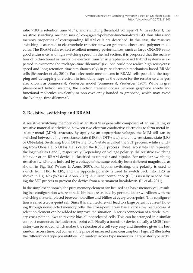
A resistive switching memory cell in an RRAM is generally composed of an insulating orresistive material sandwiched between two electron-conductive electrodes to form metal-in‐sulator-metal (MIM) structure. By applying an appropriate voltage, the MIM cell can beswitched between a high-resistance state (HRS or OFF-state) and a low-resistance state (LRSor ON-state). Switching from OFF-state to ON-state is called the SET process, while switch‐ing from ON-state to OFF-state is called the RESET process. These two states can representthe logic values 1 and 0, respectively. Depending on voltage polarity, the resistive switchingbehavior of an RRAM device is classified as unipolar and bipolar. For unipolar switching,resistive switching is induced by a voltage of the same polarity but a different magnitude, asshown in Fig. 1(a) (Waser & Aono, 2007). For bipolar switching, one polarity is used toswitch from HRS to LRS, and the opposite polarity is used to switch back into HRS, asshown in Fig. 1(b) (Waser & Aono, 2007). A current compliance (CC) is usually needed dur‐ing the SET process to prevent the device from a permanent breakdown. (Li et al., 2011)
In the simplest approach, the pure memory element can be used as a basic memory cell, result‐ing in a configuration where parallel bitlines are crossed by perpendicular wordlines with theswitching material placed between wordline and bitline at every cross-point. This configura‐tion is called a cross-point cell. Since this architecture will lead to a large parasitic current flow‐ing through nonselected memory cells, the cross-point array has a very slow read access. Aselection element can be added to improve the situation. A series connection of a diode in ev‐ery cross-point allows to reverse bias all nonselected cells. This can be arranged in a similarcompact manner as the basic cross-point cell. Finally a transistor device (ideally a MOS Tran‐sistor) can be added which makes the selection of a cell very easy and therefore gives the bestrandom access time, but comes at the price of increased area consumption. Figure 2 illustratesthe different cell type possibilities. For random access type memories, a transistor type archi‐
Advances in Resistive Switching Memories Based on Graphene Oxidehttp://dx.doi.org/10.5772/51260
187
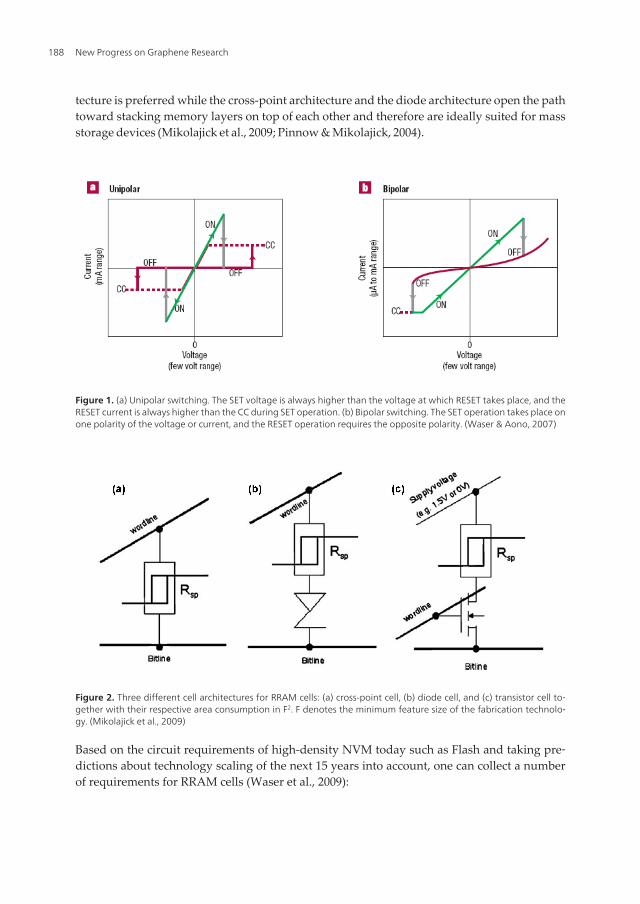
tecture is preferred while the cross-point architecture and the diode architecture open the pathtoward stacking memory layers on top of each other and therefore are ideally suited for massstorage devices (Mikolajick et al., 2009; Pinnow & Mikolajick, 2004).
Figure 1. (a) Unipolar switching. The SET voltage is always higher than the voltage at which RESET takes place, and theRESET current is always higher than the CC during SET operation. (b) Bipolar switching. The SET operation takes place onone polarity of the voltage or current, and the RESET operation requires the opposite polarity. (Waser & Aono, 2007)
Figure 2. Three different cell architectures for RRAM cells: (a) cross-point cell, (b) diode cell, and (c) transistor cell to‐gether with their respective area consumption in F2. F denotes the minimum feature size of the fabrication technolo‐gy. (Mikolajick et al., 2009)
Based on the circuit requirements of high-density NVM today such as Flash and taking pre‐dictions about technology scaling of the next 15 years into account, one can collect a numberof requirements for RRAM cells (Waser et al., 2009):
New Progress on Graphene Research188
2.1. Write operation
Write voltages should be in the range of a few hundred mV to be compatible with scaledCMOS to few V (to give an advantage over Flash which suffers from high programming vol‐tages). The length of write voltage pulses is desired to be <100 ns in order to compete withDRAM specifications and to outperform Flash which has a programming speed of some 10ms, or even <10 ns to approach high-performance SRAM.
2.2. Read operation
Read voltages need to be significantly smaller than write voltages in order to prevent a changeof the resistance during the read operation. Because of constraints by circuit design, read volt‐age cannot be less than approximately one tenth of write voltage. An additional requirementoriginates from the minimum read current. In the ON-state, read current should not be lessthan approximately 1mA to allow for a fast detection of the state by reasonably small sense am‐plifiers. The read time must be in the order of write time or preferably shorter.
2.3. Resistance ratio
Although an ON/OFF (ROFF/RON) ratio of only 1.2 to 1.3 can be utilized by dedicated circuitdesign as shown in MRAM, ON/OFF ratios >10 are required to allow for small and highlyefficient sense amplifiers and, hence, RRAM devices which are cost competitive with Flash.
2.4. Endurance
Contemporary Flash shows a maximum number of write cycles between 103 and 107, depend‐ing on the type. RRAM should provide at least the same endurance, preferably a better one.
2.5. Retention
A data retention time of >10 years is required for universal NVM. This retention time mustbe kept at thermal stress up to 85 ºC and small electrical stress such as a constant stream ofread voltage pulses.
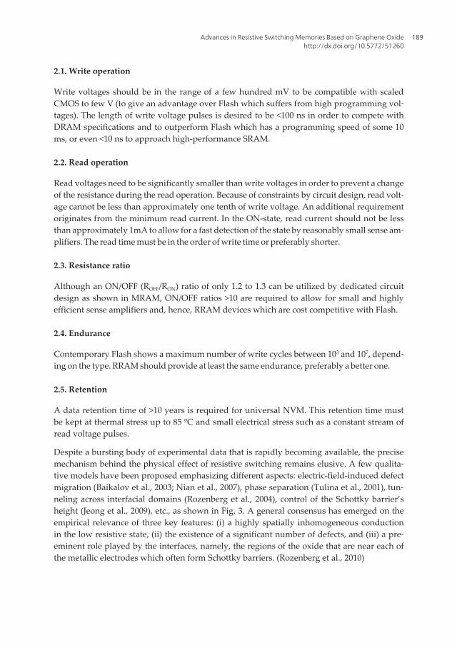
Despite a bursting body of experimental data that is rapidly becoming available, the precisemechanism behind the physical effect of resistive switching remains elusive. A few qualita‐tive models have been proposed emphasizing different aspects: electric-field-induced defectmigration (Baikalov et al., 2003; Nian et al., 2007), phase separation (Tulina et al., 2001), tun‐neling across interfacial domains (Rozenberg et al., 2004), control of the Schottky barrier’sheight (Jeong et al., 2009), etc., as shown in Fig. 3. A general consensus has emerged on theempirical relevance of three key features: (i) a highly spatially inhomogeneous conductionin the low resistive state, (ii) the existence of a significant number of defects, and (iii) a pre‐eminent role played by the interfaces, namely, the regions of the oxide that are near each ofthe metallic electrodes which often form Schottky barriers. (Rozenberg et al., 2010)
Advances in Resistive Switching Memories Based on Graphene Oxidehttp://dx.doi.org/10.5772/51260
189
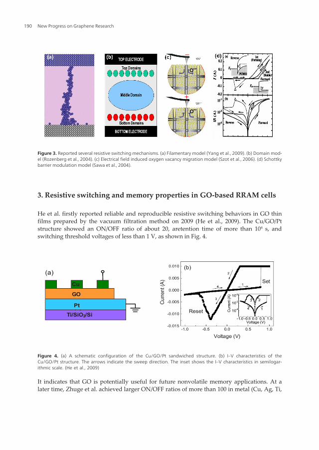
Figure 3. Reported several resistive switching mechanisms. (a) Filamentary model (Yang et al., 2009). (b) Domain mod‐el (Rozenberg et al., 2004). (c) Electrical field induced oxygen vacancy migration model (Szot et al., 2006). (d) Schottkybarrier modulation model (Sawa et al., 2004).
3. Resistive switching and memory properties in GO-based RRAM cells
He et al. firstly reported reliable and reproducible resistive switching behaviors in GO thinfilms prepared by the vacuum filtration method on 2009 (He et al., 2009). The Cu/GO/Ptstructure showed an ON/OFF ratio of about 20, aretention time of more than 104 s, andswitching threshold voltages of less than 1 V, as shown in Fig. 4.
Figure 4. (a) A schematic configuration of the Cu/GO/Pt sandwiched structure. (b) I–V characteristics of theCu/GO/Pt structure. The arrows indicate the sweep direction. The inset shows the I–V characteristics in semilogar‐ithmic scale. (He et al., 2009)
It indicates that GO is potentially useful for future nonvolatile memory applications. At alater time, Zhuge et al. achieved larger ON/OFF ratios of more than 100 in metal (Cu, Ag, Ti,
New Progress on Graphene Research190
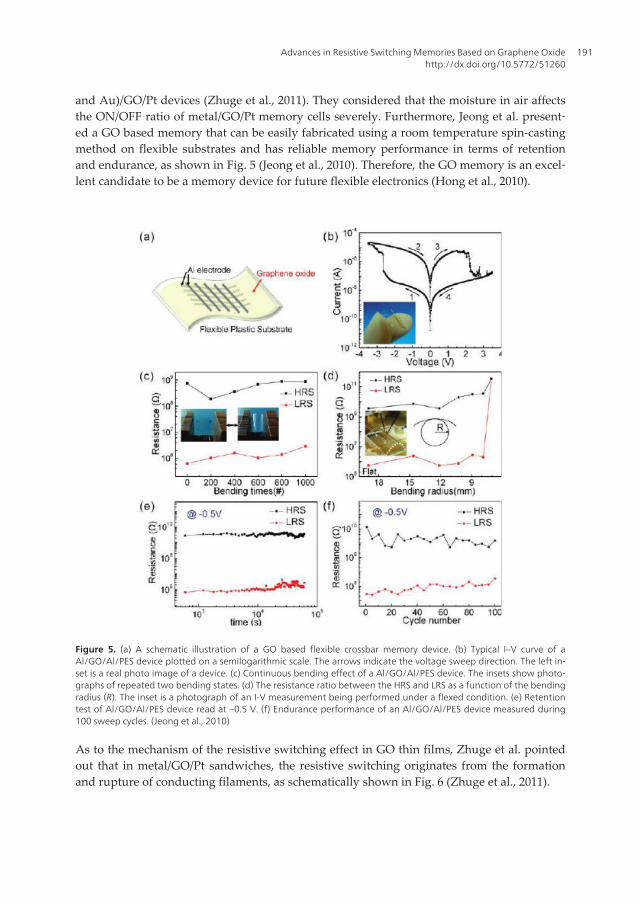
and Au)/GO/Pt devices (Zhuge et al., 2011). They considered that the moisture in air affectsthe ON/OFF ratio of metal/GO/Pt memory cells severely. Furthermore, Jeong et al. present‐ed a GO based memory that can be easily fabricated using a room temperature spin-castingmethod on flexible substrates and has reliable memory performance in terms of retentionand endurance, as shown in Fig. 5 (Jeong et al., 2010). Therefore, the GO memory is an excel‐lent candidate to be a memory device for future flexible electronics (Hong et al., 2010).
Figure 5. (a) A schematic illustration of a GO based flexible crossbar memory device. (b) Typical I–V curve of aAl/GO/Al/PES device plotted on a semilogarithmic scale. The arrows indicate the voltage sweep direction. The left in‐set is a real photo image of a device. (c) Continuous bending effect of a Al/GO/Al/PES device. The insets show photo‐graphs of repeated two bending states. (d) The resistance ratio between the HRS and LRS as a function of the bendingradius (R). The inset is a photograph of an I-V measurement being performed under a flexed condition. (e) Retentiontest of Al/GO/Al/PES device read at –0.5 V. (f) Endurance performance of an Al/GO/Al/PES device measured during100 sweep cycles. (Jeong et al., 2010)
As to the mechanism of the resistive switching effect in GO thin films, Zhuge et al. pointedout that in metal/GO/Pt sandwiches, the resistive switching originates from the formationand rupture of conducting filaments, as schematically shown in Fig. 6 (Zhuge et al., 2011).
Advances in Resistive Switching Memories Based on Graphene Oxidehttp://dx.doi.org/10.5772/51260
191

Figure 6. A schematic diagram for the mechanism of the resistive switching in metal/GO/Pt memory cells.(Zhuge et al., 2011)
Figure 7. (a), (b) and (c) AFM images of virgin GO films, GO films in LRS, and GO films in HRS. The light-coloredribbons represent folded regions. (d), (e) and (f) the corresponding CAFM images under a read voltage of 1 V.(Zhuge et al., 2011)
An analysis of the temperature dependence of the ON-state resistance reveals that the fila‐ments are composed of metal atoms due to the diffusion of the top electrodes under a biasvoltage. Tsuruoka et al. pointed out that the formation of a metal filament is due to inhomo‐geneous nucleation and subsequent growth of metal, based on the migration of metal ions inthe oxide matrix (Tsuruoka et al., 2010). Recently, they reported that the ionization of metalat the anode interfaces is likely to be attributed to chemical oxidation via residual water inthe oxide layer, and metal ions migrate along grain boundaries in the oxide layer, where ahydrogen-bond network might be formed by moisture absorption (Tsuruoka et al., 2012).Moreover, the switching occurs within confined regions of the metal filaments. The RESETprocess is considered to consist of the Joule-heating-assisted oxidation of metal atoms at thethinnest part of the metal filament followed by diffusion and drift of the metal ions under
New Progress on Graphene Research192

their own concentration gradient and the applied electric field, disconnecting the metal fila‐ment (Tsuruoka et al., 2010). Zhuge et al. also observed the resistive switching effect inGO/Pt structures by conducting atomic force microscopy (CAFM), as shown in Fig. 7 (Zhugeet al., 2011). It is attributed to the redox reactions between GO and adsorbed water inducedby external voltage biases. While for Al/GO/Al memory cells, Jeong et al. attributed the bi‐polar resistive switching behavior to rupture and formation of conducting filaments at thetop amorphous interface layer formed between the GO film and the top Al metal electrode,as shown in Fig. 8 (Jeong et al, 2010).
Figure 8. Schematic of the proposed bipolar resistive switching model for Al electrode/GO/Al electrode crossbarmemory device. (a) The pristine device is in the OFF-state due to the (relatively) thick insulating top interface layerformed by a redox reaction between vapor deposited Al and the GO thin film. (b) The ON-state is induced by the for‐mation of local filaments in the top interface layer due to oxygen ion diffusion back into the GO thin film by an exter‐nal negative bias on the top electrode. (Jeong et al., 2010)
Furthermore, Hong et al. pointed out that for Al/GO/metal memory devices, the resistiveswitching operation is governed by dual mechanism of oxygen migration and Al diffusion(Hong et al., 2011). The Al diffusion into the graphene oxide is the main factor to determinethe switching endurance property which limits the long term lifetime of the device. The elec‐trode dependence on graphene oxide RRAM operation has been analyzed as well and is at‐tributed to the difference in surface roughness of graphene oxide for the different bottomelectrodes, as shown in Fig. 9 (Hong et al., 2011). Interestingly, Panin et al. observed bothdiode-like (rectifying) and resistor-like (nonrectifying) resistive switching behaviors in anAl/GO/Al planar structure, as shown in Fig. 10 (Panin et al., 2011). Electrical characterizationof the Al/GO interface using the induced current identifies a potential barrier near the inter‐face and its spatial modulation, caused by local changes of resistance at a bias voltage,
Advances in Resistive Switching Memories Based on Graphene Oxidehttp://dx.doi.org/10.5772/51260
193
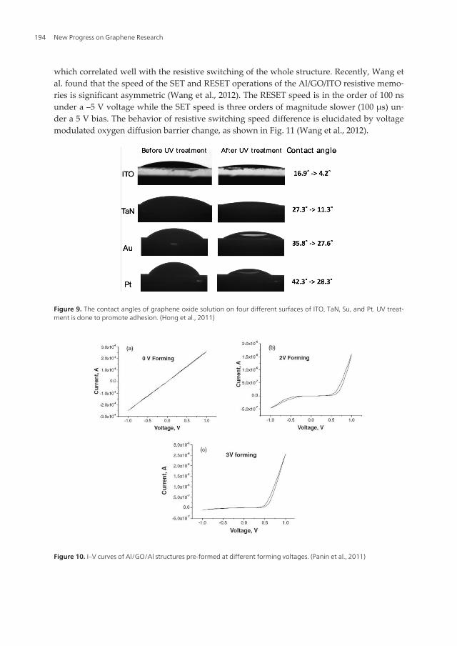
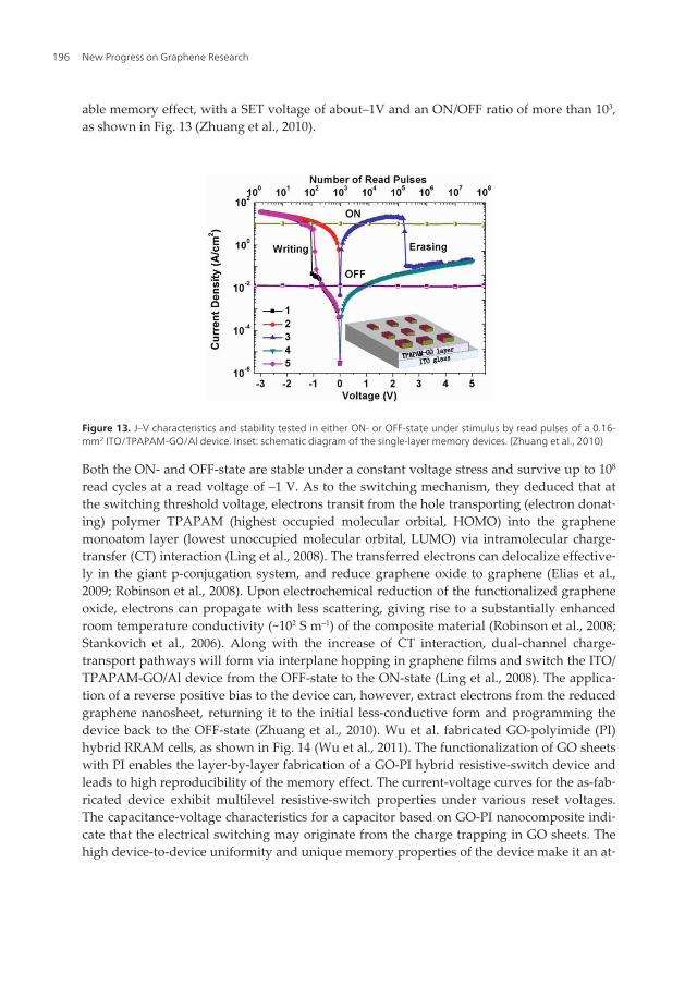
which correlated well with the resistive switching of the whole structure. Recently, Wang etal. found that the speed of the SET and RESET operations of the Al/GO/ITO resistive memo‐ries is significant asymmetric (Wang et al., 2012). The RESET speed is in the order of 100 nsunder a –5 V voltage while the SET speed is three orders of magnitude slower (100 μs) un‐der a 5 V bias. The behavior of resistive switching speed difference is elucidated by voltagemodulated oxygen diffusion barrier change, as shown in Fig. 11 (Wang et al., 2012).
Figure 9. The contact angles of graphene oxide solution on four different surfaces of ITO, TaN, Su, and Pt. UV treat‐ment is done to promote adhesion. (Hong et al., 2011)
Figure 10. I–V curves of Al/GO/Al structures pre-formed at different forming voltages. (Panin et al., 2011)
New Progress on Graphene Research194
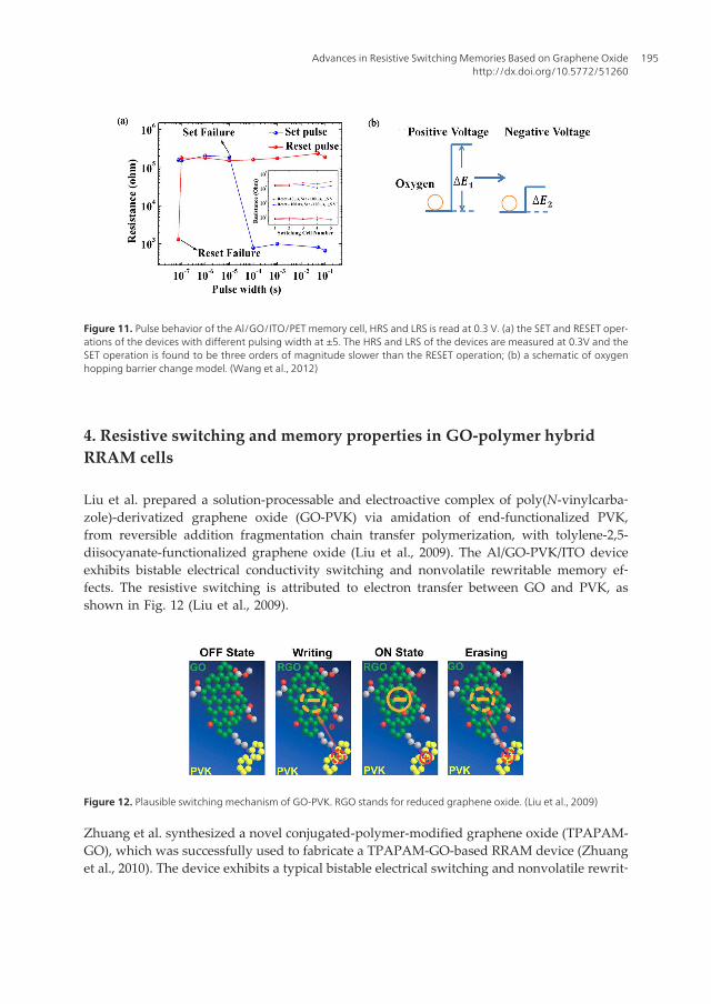
Figure 11. Pulse behavior of the Al/GO/ITO/PET memory cell, HRS and LRS is read at 0.3 V. (a) the SET and RESET oper‐ations of the devices with different pulsing width at ±5. The HRS and LRS of the devices are measured at 0.3V and theSET operation is found to be three orders of magnitude slower than the RESET operation; (b) a schematic of oxygenhopping barrier change model. (Wang et al., 2012)
4. Resistive switching and memory properties in GO-polymer hybridRRAM cells
Liu et al. prepared a solution-processable and electroactive complex of poly(N-vinylcarba‐zole)-derivatized graphene oxide (GO-PVK) via amidation of end-functionalized PVK,from reversible addition fragmentation chain transfer polymerization, with tolylene-2,5-diisocyanate-functionalized graphene oxide (Liu et al., 2009). The Al/GO-PVK/ITO deviceexhibits bistable electrical conductivity switching and nonvolatile rewritable memory ef‐fects. The resistive switching is attributed to electron transfer between GO and PVK, asshown in Fig. 12 (Liu et al., 2009).
Figure 12. Plausible switching mechanism of GO-PVK. RGO stands for reduced graphene oxide. (Liu et al., 2009)
Zhuang et al. synthesized a novel conjugated-polymer-modified graphene oxide (TPAPAM-GO), which was successfully used to fabricate a TPAPAM-GO-based RRAM device (Zhuanget al., 2010). The device exhibits a typical bistable electrical switching and nonvolatile rewrit‐
Advances in Resistive Switching Memories Based on Graphene Oxidehttp://dx.doi.org/10.5772/51260
195
able memory effect, with a SET voltage of about–1V and an ON/OFF ratio of more than 103,as shown in Fig. 13 (Zhuang et al., 2010).
Figure 13. J–V characteristics and stability tested in either ON- or OFF-state under stimulus by read pulses of a 0.16-mm2 ITO/TPAPAM-GO/Al device. Inset: schematic diagram of the single-layer memory devices. (Zhuang et al., 2010)
Both the ON- and OFF-state are stable under a constant voltage stress and survive up to 108
read cycles at a read voltage of –1 V. As to the switching mechanism, they deduced that atthe switching threshold voltage, electrons transit from the hole transporting (electron donat‐ing) polymer TPAPAM (highest occupied molecular orbital, HOMO) into the graphenemonoatom layer (lowest unoccupied molecular orbital, LUMO) via intramolecular charge-transfer (CT) interaction (Ling et al., 2008). The transferred electrons can delocalize effective‐ly in the giant p-conjugation system, and reduce graphene oxide to graphene (Elias et al.,2009; Robinson et al., 2008). Upon electrochemical reduction of the functionalized grapheneoxide, electrons can propagate with less scattering, giving rise to a substantially enhancedroom temperature conductivity (~102 S m–1) of the composite material (Robinson et al., 2008;Stankovich et al., 2006). Along with the increase of CT interaction, dual-channel charge-transport pathways will form via interplane hopping in graphene films and switch the ITO/TPAPAM-GO/Al device from the OFF-state to the ON-state (Ling et al., 2008). The applica‐tion of a reverse positive bias to the device can, however, extract electrons from the reducedgraphene nanosheet, returning it to the initial less-conductive form and programming thedevice back to the OFF-state (Zhuang et al., 2010). Wu et al. fabricated GO-polyimide (PI)hybrid RRAM cells, as shown in Fig. 14 (Wu et al., 2011). The functionalization of GO sheetswith PI enables the layer-by-layer fabrication of a GO-PI hybrid resistive-switch device andleads to high reproducibility of the memory effect. The current-voltage curves for the as-fab‐ricated device exhibit multilevel resistive-switch properties under various reset voltages.The capacitance-voltage characteristics for a capacitor based on GO-PI nanocomposite indi‐cate that the electrical switching may originate from the charge trapping in GO sheets. Thehigh device-to-device uniformity and unique memory properties of the device make it an at‐
New Progress on Graphene Research196
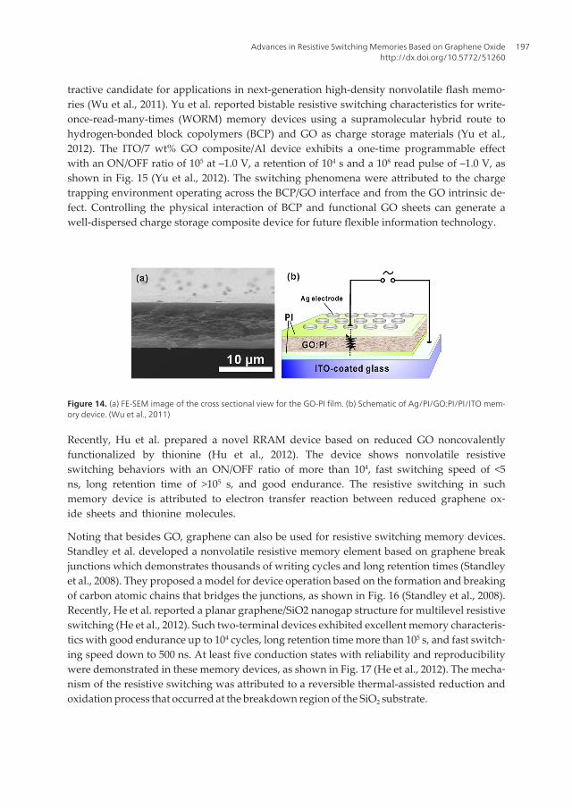
tractive candidate for applications in next-generation high-density nonvolatile flash memo‐ries (Wu et al., 2011). Yu et al. reported bistable resistive switching characteristics for write-once-read-many-times (WORM) memory devices using a supramolecular hybrid route tohydrogen-bonded block copolymers (BCP) and GO as charge storage materials (Yu et al.,2012). The ITO/7 wt% GO composite/Al device exhibits a one-time programmable effectwith an ON/OFF ratio of 105 at –1.0 V, a retention of 104 s and a 108 read pulse of –1.0 V, asshown in Fig. 15 (Yu et al., 2012). The switching phenomena were attributed to the chargetrapping environment operating across the BCP/GO interface and from the GO intrinsic de‐fect. Controlling the physical interaction of BCP and functional GO sheets can generate awell-dispersed charge storage composite device for future flexible information technology.
Figure 14. (a) FE-SEM image of the cross sectional view for the GO-PI film. (b) Schematic of Ag/PI/GO:PI/PI/ITO mem‐ory device. (Wu et al., 2011)
Recently, Hu et al. prepared a novel RRAM device based on reduced GO noncovalentlyfunctionalized by thionine (Hu et al., 2012). The device shows nonvolatile resistiveswitching behaviors with an ON/OFF ratio of more than 104, fast switching speed of <5ns, long retention time of >105 s, and good endurance. The resistive switching in suchmemory device is attributed to electron transfer reaction between reduced graphene ox‐ide sheets and thionine molecules.
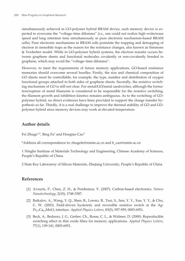
Noting that besides GO, graphene can also be used for resistive switching memory devices.Standley et al. developed a nonvolatile resistive memory element based on graphene breakjunctions which demonstrates thousands of writing cycles and long retention times (Standleyet al., 2008). They proposed a model for device operation based on the formation and breakingof carbon atomic chains that bridges the junctions, as shown in Fig. 16 (Standley et al., 2008).Recently, He et al. reported a planar graphene/SiO2 nanogap structure for multilevel resistiveswitching (He et al., 2012). Such two-terminal devices exhibited excellent memory characteris‐tics with good endurance up to 104 cycles, long retention time more than 105 s, and fast switch‐ing speed down to 500 ns. At least five conduction states with reliability and reproducibilitywere demonstrated in these memory devices, as shown in Fig. 17 (He et al., 2012). The mecha‐nism of the resistive switching was attributed to a reversible thermal-assisted reduction andoxidation process that occurred at the breakdown region of the SiO2 substrate.
Advances in Resistive Switching Memories Based on Graphene Oxidehttp://dx.doi.org/10.5772/51260
197
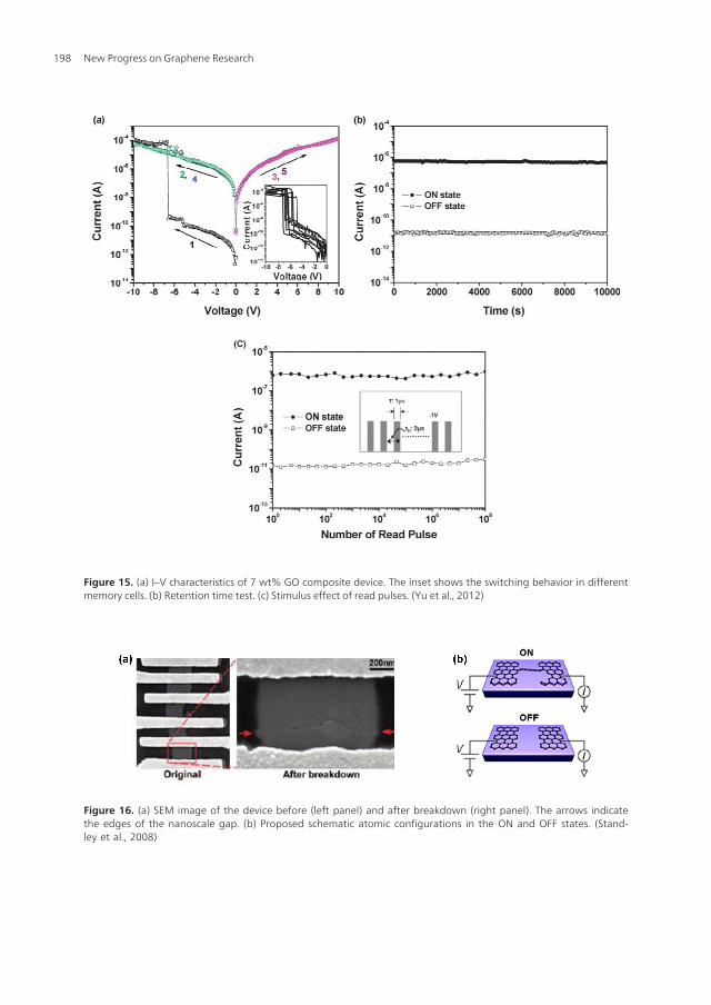
Figure 15. (a) I–V characteristics of 7 wt% GO composite device. The inset shows the switching behavior in differentmemory cells. (b) Retention time test. (c) Stimulus effect of read pulses. (Yu et al., 2012)
Figure 16. (a) SEM image of the device before (left panel) and after breakdown (right panel). The arrows indicatethe edges of the nanoscale gap. (b) Proposed schematic atomic configurations in the ON and OFF states. (Stand‐ley et al., 2008)
New Progress on Graphene Research198
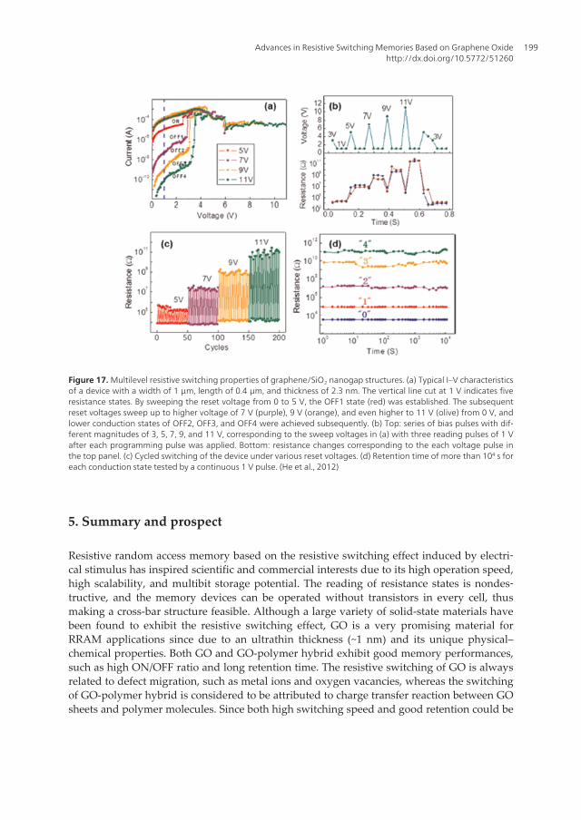
Figure 17. Multilevel resistive switching properties of graphene/SiO2 nanogap structures. (a) Typical I–V characteristicsof a device with a width of 1 μm, length of 0.4 μm, and thickness of 2.3 nm. The vertical line cut at 1 V indicates fiveresistance states. By sweeping the reset voltage from 0 to 5 V, the OFF1 state (red) was established. The subsequentreset voltages sweep up to higher voltage of 7 V (purple), 9 V (orange), and even higher to 11 V (olive) from 0 V, andlower conduction states of OFF2, OFF3, and OFF4 were achieved subsequently. (b) Top: series of bias pulses with dif‐ferent magnitudes of 3, 5, 7, 9, and 11 V, corresponding to the sweep voltages in (a) with three reading pulses of 1 Vafter each programming pulse was applied. Bottom: resistance changes corresponding to the each voltage pulse inthe top panel. (c) Cycled switching of the device under various reset voltages. (d) Retention time of more than 104 s foreach conduction state tested by a continuous 1 V pulse. (He et al., 2012)
5. Summary and prospect
Resistive random access memory based on the resistive switching effect induced by electri‐cal stimulus has inspired scientific and commercial interests due to its high operation speed,high scalability, and multibit storage potential. The reading of resistance states is nondes‐tructive, and the memory devices can be operated without transistors in every cell, thusmaking a cross-bar structure feasible. Although a large variety of solid-state materials havebeen found to exhibit the resistive switching effect, GO is a very promising material forRRAM applications since due to an ultrathin thickness (~1 nm) and its unique physical–chemical properties. Both GO and GO-polymer hybrid exhibit good memory performances,such as high ON/OFF ratio and long retention time. The resistive switching of GO is alwaysrelated to defect migration, such as metal ions and oxygen vacancies, whereas the switchingof GO-polymer hybrid is considered to be attributed to charge transfer reaction between GOsheets and polymer molecules. Since both high switching speed and good retention could be
Advances in Resistive Switching Memories Based on Graphene Oxidehttp://dx.doi.org/10.5772/51260
199
simultaneously achieved in GO-polymer hybrid RRAM device, such memory device is ex‐pected to overcome the “voltage–time dilemma” (i.e., one could not realize high write/erasespeed and long retention time simultaneously in pure electronic mechanism-based RRAMcells). Pure electronic mechanisms in RRAM cells postulate the trapping and detrapping ofelectron in immobile traps as the reason for the resistance changes, also known as Simmons& Verderber model. While in GO-polymer hybrid systems, the electron transfer occurs be‐tween graphene sheets and functional molecules covalently or non-covalently bonded tographene, which may avoid the “voltage–time dilemma”.
However, to meet the requirements of future memory applications, GO-based resistancememories should overcome several hurdles. Firstly, the size and chemical composition ofGO sheets must be controllable, for example, the type, number and distribution of oxygenfunctional groups attached to both sides of graphene sheets. Secondly, the resistive switch‐ing mechanism of GO is still not clear. For metal/GO/metal sandwiches, although the forma‐tion/rupture of metal filaments is considered to be responsible for the resistive switching,the filament growth and inhibition kinetics remains ambiguous. As to the switching of GO-polymer hybrid, no direct evidences have been provided to support the charge transfer hy‐pothesis so far. Thirdly, it is a real challenge to improve the thermal stability of GO and GO-polymer hybrid since memory devices may work at elevated temperature.
Author details
Fei Zhuge1,2*, Bing Fu1 and Hongtao Cao1*
*Address all correspondence to: [email protected] and [email protected]
1 Ningbo Institute of Materials Technology and Engineering, Chinese Academy of Sciences,People’s Republic of China
2 State Key Laboratory of Silicon Materials, Zhejiang University, People’s Republic of China
References
[1] Avouris, P., Chen, Z. H., & Perebeinos, V. (2007). Carbon-based electronics. NatureNanotechnology, 2(10), 1748-3387.
[2] Baikalov, A., Wang, Y. Q., Shen, B., Lorenz, B., Tsui, S., Sun, Y. Y., Xue, Y. Y., & Chu,C. W. (2003). Field-driven hysteretic and reversible resistive switch at the Ag-Pr0.7Ca0.3MnO3 interface. Applied Physics Letters, 83(5), 957-959, 0003-6951.
[3] Beck, A., Bednorz, J. G., Gerber, Ch., Rosse, C. L., & Widmer, D. (2000). Reproducibleswitching effect in thin oxide films for memory applications. Applied Physics Letters,77(1), 139-141, 0003-6951.
New Progress on Graphene Research200

[4] Burghard, M., Klauk, H., & Kern, K. (2009). Carbon-Based Field-Effect Transistors forNanoelectronics. Advanced Materials, 21(25-26), 2586-2600, 0935-9648.
[5] Chang, W. Y., Lai, Y. C., Wu, T. B., Wang, S. F., Chen, F., & Tsai, M. J. (2008). Unipo‐lar resistive switching characteristics of ZnO thin films for nonvolatile memory ap‐plications. Applied Physics Letters, 92(2), 22110, 0003-6951.
[6] Cote, L. J., Kim, F., & Huang, J. X. (2009). Langmuir−Blodgett Assembly of GraphiteOxide Single Layers. Journal of the American Chemical Society, 131(3), 1043-1049,0002-7863.
[7] Dong, Y., Yu, M. G., Mc Alpine, C., Lu, W., & Lieber, C. M. (2008). Si/α-Si core/shellnanowires as nonvolatile crossbar switches. Nano Letters, 8(2), 386-391, 1530-6984.
[8] Eda, G., Fanchini, G., & Chhowalla, M. (2008). Large-area ultrathin films of reducedgraphene oxide as a transparent and flexible electronic material. Nature Nanotechnolo‐gy, 3(5), 270-274, 1748-3387.
[9] Elias, D. C., Nair, R. R., Mohiuddin, T. M. G., Morozov, S. R., Blake, P., Halsall, M. P.,& Ferrari, A. C. (2009). Control of graphene’s properties by reversible hydrogenation:Evidence for graphane. Science, 323(5914), 610-613, 0036-8075.
[10] Guan, W. H., Long, S. B., Jia, R., & Liu, M. (2007). Nonvolatile resistive switchingmemory utilizing gold nanocrystals embedded in zirconium oxide. Applied PhysicsLetters, 91(6), 062111, 0003-6951.
[11] Guan, W. H., Liu, M., Long, S. B., Liu, Q., & Wang, W. (2008). On the resistive switch‐ing mechanisms of Cu/ZrO2:Cu/Pt. Applied Physics Letters, 93(22), 223506, 0003-6951.
[12] He, C. L., Zhuge, F., Zhou, X. F., Li, M., Zhou, G. C., Liu, Y. W., Wang, J. Z., Chen, B.,Su, W. J., Liu, Z. P., Wu, Y. H., Cui, P., & Li, R. W. (2009). Nonvolatile resistiveswitching in graphene oxide thin films. Applied Physics Letters, 95(23), 232101,0003-6951.
[13] He, C. L., Shi, Z. W., Zhang, L. C., Yang, W., Yang, R., Shi, D. X., & Zhang, G. Y.(2012). Multilevel resistive switching in planar graphene/SiO2 nanogap structures.ACS Nano, 6(5), 4214-4221, 1936-0851.
[14] Hong, S. K., Kim, J. E., Kim, S. O., Choi, S. Y., & Cho, B. J. (2010). Flexible resistiveswitching memory device based on graphene oxide. IEEE Electron Device Letters,31(9), 1005-1007, 0741-3106.
[15] Hong, S. K., Kim, J. E., Kim, S. O., & Cho, B. J. (2011). Analysis on switching mecha‐nism of graphene oxide resistive memory device. Journal of Applied Physics, 110(4),044506, 0021-4922.
[16] Hu, B. L., Quhe, R. G., Chen, C., Zhuge, F., Zhu, X. J., Peng, S. S., Chen, X. X., Pan, L.,Wu, Y. Z., Zheng, W. G., Yan, Q., Lu, J., & Li, R. W. (). Electrically controlled electrontransfer and resistance switching in graphene oxide noncovolently functionalized with dye,unpublished.
Advances in Resistive Switching Memories Based on Graphene Oxidehttp://dx.doi.org/10.5772/51260
201
[17] Jeong, D. S., Schroeder, H., & Waser, R. (2009). Abnormal bipolar-like resistancechange behavior induced by symmetric electroforming in Pt/TiO2/Pt resistive switch‐ing cells. Nanotechnology, 20(37), 375201, 0957-4484.
[18] Jeong, D. S., Schroeder, H., & Waser, R. (2009). Mechanism for bipolar switching in aPt/TiO2/Pt resistive switching cell. Physical Review B, 79(19), 195317, 1098-0121.
[19] Jeong, H. Y., Kim, J. Y., Kim, J. W., Hwang, J. O., Kim, J. E., Lee, J. Y., Yoon, T. H.,Cho, B. J., Kim, S. O., Ruoff, R. S., & Choi, S. Y. (2010). Graphene oxide thin films forflexible nonvolatile memory applications. Nano Letters, 10(11), 4381-4386, 1476-1122.
[20] Jo, S. H., & Lu, W. (2008). CMOS Compatible Nanoscale Nonvolatile ResistanceSwitching Memory. Nano Letters, 8(2), 392-397, 1476-1122.
[21] Jo, S. H., Kim, K. H., & Lu, W. (2009). Programmable Resistance Switching in Nano‐scale Two-Terminal Devices. Nano Letters, 9(1), 496-500, 1476-1122.
[22] Jo, S. H., Kim, K. H., & Lu, W. (2009). High-Density Crossbar Arrays Based on a SiMemristive System. Nano Letters, 9(2), 870-874, 1476-1122.
[23] Kim, D. C., Lee, M. J., Ahn, S. E., Seo, S., Park, J. C., Yoo, I. K., Baek, I. G., Kim, H. J.,Yim, E. K., Lee, J. E., Park, S. O., Kim, H. S., In, Chung. U., Moon, J. T., & Ryu, B. I.(2006). Improvement of resistive memory switching in NiO using IrO2 . Applied Phys‐ics Letters, 88(23), 232106, 0003-6951.
[24] Kim, K. M., Choi, B. J., Shin, Y. C., Choi, S., & Hwang, C. S. (2007). Anode-interfacelocalized filamentary mechanism in resistive switching of TiO2 thin films. AppliedPhysics Letters, 91(1), 012907, 0003-6951.
[25] Kim, S., Moon, H., Gupta, D., Yoo, S., & Choi, Y. K. (2009). Resistive Switching Char‐acteristics of Sol-Gel Zinc Oxide Films for Flexible Memory Applications. IEEE Trans‐actions on Electron Devices, 56(4), 696-699, 0018-9383.
[26] Kwon, D. H., Kim, K. M., Jang, J. H., Jeon, J. M., Lee, M. H., Kim, G. H., Li, X. S., Park,G. S., Lee, B., Han, S., Kim, M., & Hwang, C. S. (2010). Atomic structure of conduct‐ing nanofilaments in TiO2 resistive switching memory. Nature Nanotechnology, 5(2),148-153, 1748-3387.
[27] Lee, M. J., Park, Y., Suh, D. S., Lee, E. H., Seo, S., Kim, D. C., Jung, R., Kang, B. S.,Ahn, S. E., Lee, C. B., Seo, D. H., Cha, Y. K., Yoo, I. K., Kim, J. S., & Park, B. H. (2007).Two Series Oxide Resistors Applicable to High Speed and High Density NonvolatileMemory. Advanced Materials, 19(22), 3919-3923, 0935-9648.
[28] Li, Y. T., Long, S. B., Liu, Q., Lv, H. B., Liu, S., & Liu, M. (2011). An overview of resis‐tive random access memory devices. Chinese Science Bulletin, 56(28-29), 3072-3078,1001-6538.
[29] Liao, Z. L., Wang, Z. Z., Meng, Y., Liu, Z. Y., Gao, P., Gang, J. L., Zhao, H. W., Liang,X. J., Bai, X. D., & Chen, D. M. (2009). Categorization of resistive switching of metal-Pr0.7Ca0.3MnO3-metal devices. Applied Physics Letters, 94(25), 253503, 0003-6951.
New Progress on Graphene Research202
[30] Ling, Q. D., Liaw, D. J., Zhu, C. X., Chan, D. S. H., Kang, E. T., & Neoh, K. G. (2008).Polymer electronic memories: Materials, devices and mechanisms. Progress in Poly‐mer Sciecne, 33(10), 917-978, 0079-6700.
[31] Liu, S. Q., Wu, N. J., & Ignatiev, A. (2000). Electric-pulse-induced reversible resist‐ance change effect in magnetoresistive films. Applied Physics Letters, 76(19), 2749-2751,0003-6951.
[32] Liu, Q., Long, S. B., Wang, W., Zuo, Q. Y., Zhang, S., Chen, J. N., & Liu, M. (2009).Improvement of resistive switching properties in ZrO2-based ReRAM with implant‐ed Ti ions. IEEE Electron Device Letters, 30(12), 1335-1337, 0741-3106.
[33] Liu, G., Zhuang, X. D., Chen, Y., Zhang, B., Zhu, J. H., Zhu, C. X., Neoh, K. G., &Kang, E. T. (2009). Bistable electrical switching and electronic memory effect in a sol‐ution-processable graphene oxide-donor polymer complex. Applied Physics Letters,95(25), 253301, 0003-6951.
[34] Lu, W., & Lieber, C. M. (2007). Nanoelectronics from the bottom up. Nature Materials,6(11), 841-850, 1476-1122.
[35] Mikolajick, T., Salinga, M., Kund, M., & Kever, T. (2009). Nonvolatile memory con‐cepts based on resistive switching in inorganic materials. Advanced Engineering Mate‐rials, 11(4), 235-240, 1438-1656.
[36] Nian, Y. B., Strozier, J., Wu, N. J., Chen, X., & Ignatiev, A. (2007). Evidence for anoxygen diffusion model for the electric pulse induced resistance change effect intransition-metal oxides. Physical Review Letters, 98(14), 146403, 0031-9007.
[37] Novoselov, K. S., Geim, A. K., Morozov, S. V., Jiang, D., Zhang, Y., Dubonos, S. V.,Grigorieva, I. V., & Firsov, A. A. (2004). Electric field effect in atomically thin carbonfilms. Science, 306(5696), 666-669, 0036-8075.
[38] Odagawa, A., Sato, H., Inoue, I. H., Akoh, H., Kawasaki, M., & Tokura, Y. (2004). Co‐lossal electroresistance of a Pr0.7Ca0.3MnO3 thin film at room temperature. Physical Re‐view B, 70(22), 224403, 1098-0121.
[39] Panin, G. N., Kapitanova, O. O., Lee, S. W., Baranov, A. N., & Kang, T. W. (2011). Re‐sistive switching in Al/graphene oxide/Al structure. Japanese Journal of Applied Phys‐ics, 50(7), 070110, 0021-4922.
[40] Pinnow, C. U., & Mikolajick, T. (2004). Material aspects in emerging nonvolatilememories. Journal of the Electrochemical Society, 151(6), K13-K19, 0013-4651.
[41] Robinson, J. T., Perkins, F. K., Snow, E. S., Wei, Z., & Sheehan, P. E. (2008). Reducedgraphene oxide molecular sensors. Nano Letters, 8(10), 3137-3140, 1476-1122.
[42] Rozenberg, M. J., Inoue, I. H., & Sanchez, M. J. (2004). Nonvolatile memory with mul‐tilevel switching: A basic model. Physical Review Letters, 92(17), 178302, 0031-9007.
Advances in Resistive Switching Memories Based on Graphene Oxidehttp://dx.doi.org/10.5772/51260
203
[43] Rozenberg, M. J., Sanchez, M. J., Weht, R., Acha, C., Gomez-Marlasca, F., & Levy, P.(2010). Mechanism for bipolar resistive switching in transition-metal oxides. PhysicalReview B, 81(11), 115101, 1098-0121.
[44] Rueckes, T., Kim, K., Joselevich, E., Tseng, G. Y., Cheung, C. L., & Lieber, C. M.(2000). Carbon nanotube-based nonvolatile random access memory for molecularcomputing. Science, 289(5476), 94-97, 0036-8075.
[45] Sawa, A., Fujii, T., Kawasaki, M., & Tokura, Y. (2004). Hysteretic current-voltagecharacteristics and resistance switching at a rectifying Ti/Pr0.7Ca0.3MnO3 interface. Ap‐plied Physics Letters, 85(18), 4073-4075, 0003-6951.
[46] Schroeder, H., Zhirnov, V. V., Cavin, R. K., & Waser, R. (2010). Voltage-time dilemmaof pure electronic mechanisms in resistive switching memory cells. Journal of AppliedPhysics, 107(5), 054517, 0021-4922.
[47] Seo, S., Lee, M. J., Seo, D. H., Jeoung, E. J., Suh, D. S., Joung, Y. S., Yoo, I. K., Hwang,I. R., Kim, S. H., Byun, I. S., Kim, J. S., Choi, J. S., & Park, B. H. (2004). Reproducibleresistance switching in polycrystalline NiO films. Applied Physics Letters, 85(23),5655-5657, 0003-6951.
[48] Simmons, J. G., & Verderber, R. R. (1967). New conduction and reversible memoryphenomena in thin insulating films. Proceedings of the Royal Society of London Series A-Mathematical and Physical Sciences, 301(1464), 77, 1364-5021.
[49] Sinitskii, A., & Tour, J. M. (2009). Lithographic graphitic memories. ACS Nano, 3(9),2760-2766, 1936-0851.
[50] Son, J. Y., & Shin, Y. H. (2008). Direct observation of conducting filaments on resis‐tive switching of NiO thin films. Applied Physics Letters, 92(22), 222106, 0003-6951.
[51] Standlety, B., Bao, W. Z., Zhang, H., Bruck, J., Lau, C. N., & Bockrath, M. (2008). Gra‐phene-based atomic-scale switches. Nano Letters, 8(10), 3345-3349, 1476-1122.
[52] Stankovich, S., Dikin, D. A., Dommett, G. H. B., Kohlhaas, K. M., Zimney, E. J., Stach,E. A., Piner, R. D., Nguyen, S. T., & Ruoff, R. S. (2006). Graphene-based compositematerials. Nature, 442(7100), 282-286, 0028-0836.
[53] Stewart, D. R., Ohlberg, D. A. A., Beck, P. A., Chen, Y., Williams, R. S., Jeppesen, J.O., Nielsen, K. A., & Stoddart, J. F. (2004). Molecule-Independent Electrical Switchingin Pt/Organic Monolayer/Ti Devices. Nano Letters, 4(1), 133-136, 1476-1122.
[54] Szot, K., Speier, W., Bihlmayer, G., & Waser, R. (2006). Switching the electrical resist‐ance of individual dislocations in single-crystalline SrTiO3 . Nature Materials, 5(4),312-320, 1476-1122.
[55] Tsuruoka, T., Terabe, K., Hasegawa, T., & Aono, M. (2010). Forming and switchingmechanisms of a cation-migration-based oxide resistive memory. Nanotechnology,21(42), 425205, 0957-4484.
New Progress on Graphene Research204
[56] Tsuruoka, T., Terabe, K., Hasegawa, T., Valov, I., Waser, R., & Aono, M. (2012). Ef‐fects of moisture on the switching characteristics of oxide-based, gapless-type atomicswitches. Advanced Functional Materials, 22(1), 70-77, 1616-301X.
[57] Tulina, N. A., Zver’kov, S. A., Mukovskii, Y. M., & Shulyatev, D. A. (2001). Currentswitching of resistive states in normal-metal manganite single-crystal point contacts.Europhysics Letters, 56(6), 836-841, 1286-4854.
[58] Wang, L. H., Yang, W., Sun, Q. Q., Zhou, P., Lu, H. L., Ding, S. J., & Zhang, D. W.(2012). The mechanism of the asymmetric SET and RESET speed of graphene oxidebased flexible resistive switching memories. Applied Physics Letters, 100(6), 063509,0003-6951.
[59] Wang, X. R., Ouyang, Y. J., Li, X. L., Wang, H. L., Guo, J., & Dai, H. J. (2008). Room-Temperature All-Semiconducting Sub-10-nm Graphene Nanoribbon Field-EffectTransistors. Physical Review Letters, 100(20), 206803, 0031-9007.
[60] Waser, R., & Aono, M. (2007). Nanoionics-based resistive switching memories. Na‐ture Materials, 6(11), 833-840, 1476-1122.
[61] Waser, R., Dittmann, R., Staikov, G., & Szot, K. (2009). Redox-based resistive switch‐ing memories-Nanoionic mechanisms, prospects, and challenges. Advanced Materials,21(25-26), 2632-2663, 1476-1122.
[62] Wu, X., Zhou, P., Li, J., Chen, L. Y., Lv, H. B., Lin, Y. Y., & Tang, T. A. (2007). Repro‐ducible unipolar resistance switching in stoichiometric ZrO2 films. Applied PhysicsLetters, 90(18), 183507, 0003-6951.
[63] Wu, C. X., Li, F. S., Zhang, Y. A., Guo, T. L., & Chen, T. (2011). Highly reproduciblememory effect of organic multilevel resistive-switch device utilizing graphene oxidesheets/polyimide hybrid nanocomposite. Applied Physics Letters, 99(4), 042108,0003-6951.
[64] Yang, C. H., Seidel, J., Kim, S. Y., Rossen, P. B., Yu, P., Gajek, M., Chu, Y. H., Martin,L. W., Holcomb, M. B., He, Q., Maksymovych, P., Balke, N., Kalinin, S. V., Baddorf,A. P., Basu, S. R., et al. (2009). Electric modulation of conduction in multiferroic Ca-doped BiFeO3 films. Nature Materials, 8(6), 485-493, 1476-1122.
[65] Yang, Y. C., Pan, F., Liu, Q., Liu, M., & Zeng, F. (2009). Fully Room-Temperature-Fab‐ricated Nonvolatile Resistive Memory for Ultrafast and High-Density Memory Ap‐plication. Nano Letters, 9(4), 1636-1643, 1476-1122.
[66] Yin, K. B., Li, M., Liu, Y. W., He, C. L., Zhuge, F., Chen, B., Lu, W., Pan, X. Q., & Li, R.W. (2010). Resistance switching in polycrystalline BiFeO3 thin films. Applied PhysicsLetters, 97(4), 042101, 0003-6951.
[67] Yu, A. D., Liu, C. L., & Chen, W. C. (2012). Supramolecular block copolymers: gra‐phene oxide composites for memory device applications. Chemical Communications,48(3), 383-385, 1359-7345.
Advances in Resistive Switching Memories Based on Graphene Oxidehttp://dx.doi.org/10.5772/51260
205
[68] Zhuang, X. D., Chen, Y., Liu, G., Li, P. P., Zhu, C. X., Kang, E. T., Neoh, K. G., Zhang,B., Zhu, J. H., & Li, Y. X. (2010). Conjugated-polymer-functionalized graphene oxide:Synthesis and nonvolatile rewritable memory effect. Advanced Materials, 22(15),1731-1735, 1476-1122.
[69] Zhuge, F., Dai, W., He, C. L., Wang, A. Y., Liu, Y. W., Li, M., Wu, Y. H., Cui, P., & Li,R. W. (2010). Nonvolatile resistive switching memory based on amorphous carbon.Applied Physics Letters, 96(16), 163505, 0003-6951.
[70] Zhuge, F., Hu, B. L., He, C. L., Zhou, X. F., Liu, Z. P., & Li, R. W. (2011). Mechanismof nonvolatile resistive switching in graphene oxide thin films. Carbon, 49(12),3796-3802, 0008-6223.
[71] Zhuge, F., Li, R. W., He, C. L., Liu, Z. P., & Zhou, X. F. (2011, Mar.) Non-volatile resis‐tive switching in graphene oxide thin films. Physics and Applications of Graphene-Ex‐periments, 421-438, Print, 978-953-307-217-3, Croatia, InTech.
New Progress on Graphene Research206