Embed Size (px)
Citation preview

Advanced solutions for Minority Carrier Lifetime measurements in thin epitaxial layers G.Borionetti (a), Miklos Tallian (b), Ferenc Korsos(b), Peter Tutto(b), Markus Pfeffer (c), R. Oechsner(c) (a) MEMC Electronic Materials SpA Viale Gherzi,31 28100 Novara Italy
(b) SEMILAB Semiconductor Physics Laboratory Co,Ltd Prielle Kornelia,2 H-1117 Budapest Hungary
(c) Fraunhofer Institut Integrierte Systeme und Bauelementetechnologie Schottkystrasse,10 91058 Erlangen Germany

Introduction
• Typical substrate for photo optical devices applications is silicon epitaxial wafer where the epi layer of few micron thickness has different electrical and material characteristics than substrate
• Detection and control of transition metal traces in the device active region is fundamental for such device family (dark currenty, white spots)
EPI LAYER ex P silicon
SUBSTRATEex P+silicon

Introduction cont
• Carrier recombination lifetime is the most frequently used technique to monitor residual metals in semiconductor wafers although it’s proper determination could be difficult, since the carrier lifetime itself depends on the measurement conditions (p/n type, resistivity and injection level, steady state or transient measurement, layer structure)
• The performance of conventional contactless lifetime measurement techniques (MW-PCD, QSS-PCD) is poor on p/p+ epi structures due to the deep sampling volume and the small relative photo-conductance change. Dedicated lifetime monitor wafers (P/P) are generally used in the industry to avoid this problem.
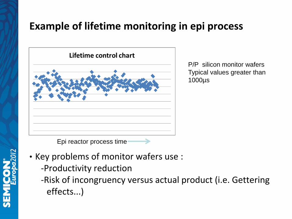
Example of lifetime monitoring in epi process
• Key problems of monitor wafers use : -Productivity reduction -Risk of incongruency versus actual product (i.e. Gettering effects...)
Epi reactor process time
P/P silicon monitor wafers
Typical values greater than
1000µs

Purpose of the work
• To develop a novel technique able to measure minority carrier lifetime only in the thin epi layer where devices are fabricated and/or patterned wafers
• The development is running inside the EU funded Project
Semiconductor Equipment Assessment Leveraging Innovation (SEAL)
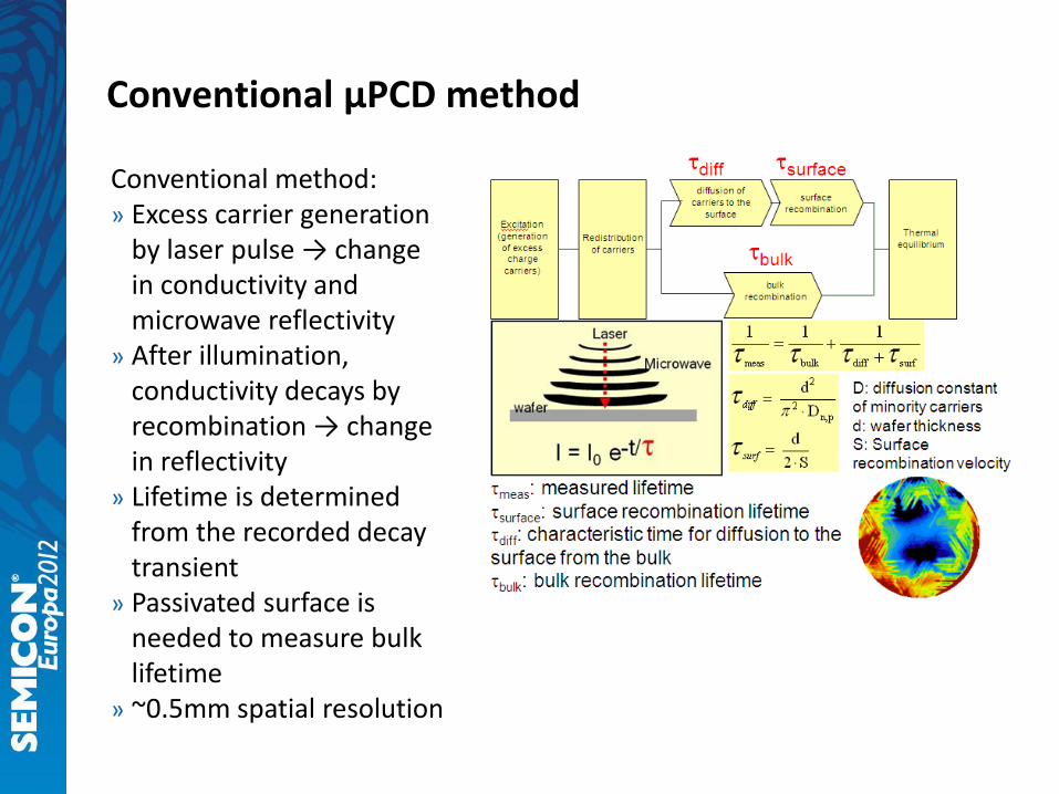
Conventional µPCD method
Conventional method: » Excess carrier generation
by laser pulse → change in conductivity and microwave reflectivity
» After illumination, conductivity decays by recombination → change in reflectivity
» Lifetime is determined from the recorded decay transient
» Passivated surface is needed to measure bulk lifetime
» ~0.5mm spatial resolution
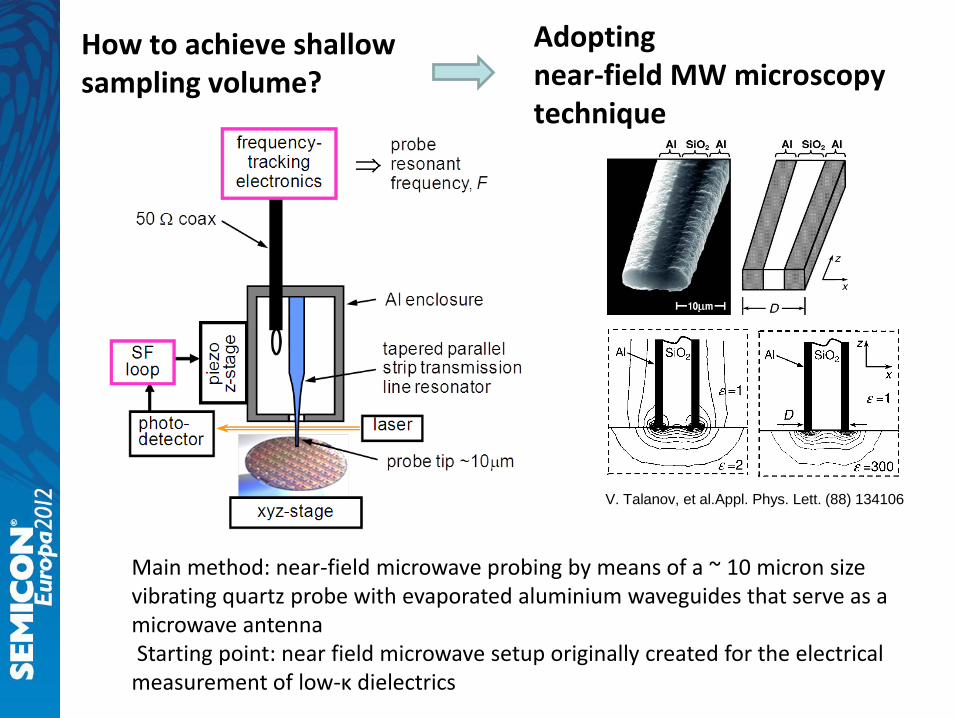
How to achieve shallow sampling volume?
Main method: near-field microwave probing by means of a ~ 10 micron size vibrating quartz probe with evaporated aluminium waveguides that serve as a microwave antenna Starting point: near field microwave setup originally created for the electrical measurement of low-κ dielectrics
Adopting near-field MW microscopy technique
V. Talanov, et al.Appl. Phys. Lett. (88) 134106

And combine with excess carrier generation near field MW photoconductance decay (NF-MW-PCD)
Near field method: » Probe is <100nm distance from the
sample » Probe vibrates mechanically, and as it
approaches the sample vibration is reduced, this controls distance
» Microwave is introduced into the probe through the Al waveguide
» A near field is created at the end of the probe (retains the properties of a static field, extends to about a 10 μm bubble)
laser
» Resonant frequency is measured » Light is introduced onto the sample, causing change in conductance » Steady-state light: resonant frequency shitfs due to illumination, shift is
measured (steady state method) » Pulse laser: Frequency is kept, reflected MW power changes due to
conductance change, this is monitored in time (transient method)

Two ways: steady state or transient method
Steady state: Steady state light (I0) Δn Δσ ΔF (resonant freq. change ) G – monotonic function The photo-effect was observed: Seems to be promising for bulk wafers – but proper evaluation for p/p+ is problematic, too much impact of resistivity and oxide thick.
Transient: Pulse light Δn (t) Frequency is fixed – reflected MW
power is changing in time Δn(t) Δσ(t) ΔPMW(t) Transient can be recorded: Lifetime is directly calculated from
the decay time – does not need calibration
Freq. shift in dark
Freq. shift illuminated
ΔF
0 /eff epin I d
0
( )F
G nF
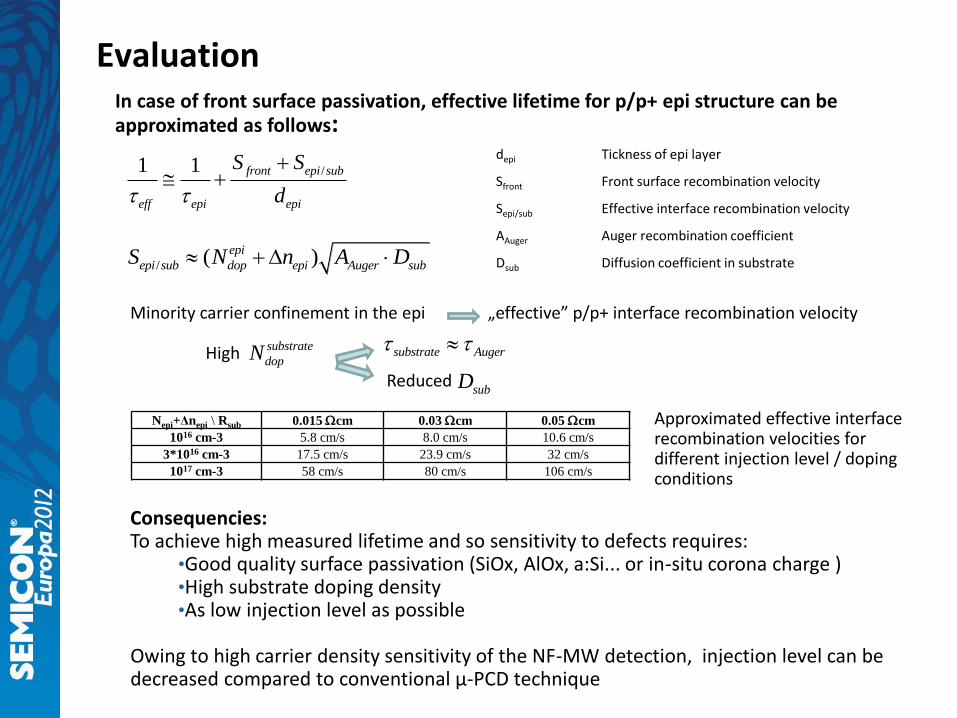
Evaluation In case of front surface passivation, effective lifetime for p/p+ epi structure can be approximated as follows:
/1 1 front epi sub
eff epi epi
S S
d
/ ( )epi
epi sub dop epi Auger subS N n A D
Nepi+Δnepi \ Rsub 0.015 cm 0.03 cm 0.05 cm
1016 cm-3 5.8 cm/s 8.0 cm/s 10.6 cm/s
3*1016 cm-3 17.5 cm/s 23.9 cm/s 32 cm/s
1017 cm-3 58 cm/s 80 cm/s 106 cm/s
depi Tickness of epi layer
Sfront Front surface recombination velocity
Sepi/sub Effective interface recombination velocity
AAuger Auger recombination coefficient
Dsub Diffusion coefficient in substrate
Minority carrier confinement in the epi „effective” p/p+ interface recombination velocity High
Approximated effective interface recombination velocities for different injection level / doping conditions
Consequencies: To achieve high measured lifetime and so sensitivity to defects requires:
•Good quality surface passivation (SiOx, AlOx, a:Si... or in-situ corona charge ) •High substrate doping density •As low injection level as possible
Owing to high carrier density sensitivity of the NF-MW detection, injection level can be decreased compared to conventional µ-PCD technique
substrate
dopN substrate Auger
subDReduced
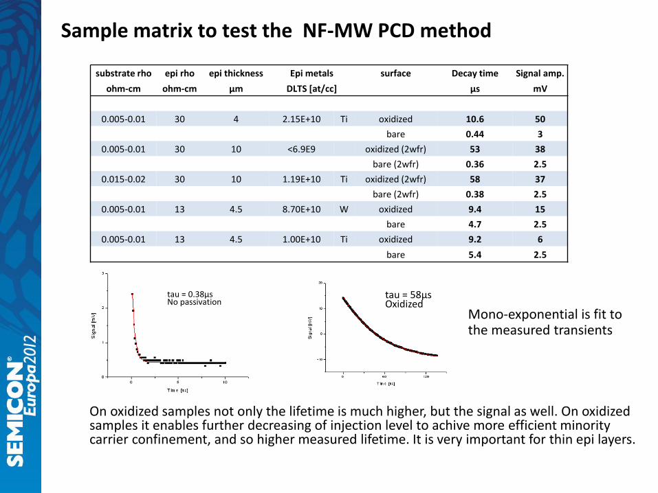
Sample matrix to test the NF-MW PCD method
On oxidized samples not only the lifetime is much higher, but the signal as well. On oxidized samples it enables further decreasing of injection level to achive more efficient minority carrier confinement, and so higher measured lifetime. It is very important for thin epi layers.
substrate rho epi rho epi thickness Epi metals surface Decay time Signal amp.
ohm-cm ohm-cm µm DLTS [at/cc] µs mV
0.005-0.01 30 4 2.15E+10 Ti oxidized 10.6 50
bare 0.44 3
0.005-0.01 30 10 <6.9E9 oxidized (2wfr) 53 38
bare (2wfr) 0.36 2.5
0.015-0.02 30 10 1.19E+10 Ti oxidized (2wfr) 58 37
bare (2wfr) 0.38 2.5
0.005-0.01 13 4.5 8.70E+10 W oxidized 9.4 15
bare 4.7 2.5
0.005-0.01 13 4.5 1.00E+10 Ti oxidized 9.2 6
bare 5.4 2.5
tau = 0.38µs No passivation
tau = 58µs Oxidized
Mono-exponential is fit to the measured transients
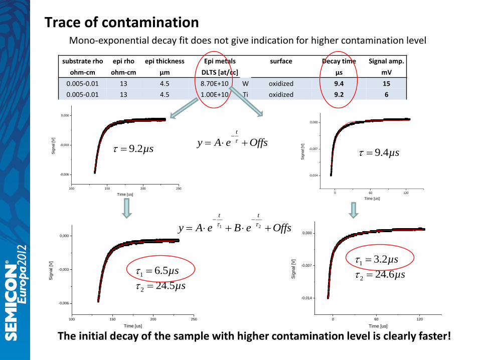
Trace of contamination Mono-exponential decay fit does not give indication for higher contamination level
substrate rho epi rho epi thickness Epi metals surface Decay time Signal amp.
ohm-cm ohm-cm µm DLTS [at/cc] µs mV
0.005-0.01 13 4.5 8.70E+10 W oxidized 9.4 15
0.005-0.01 13 4.5 1.00E+10 Ti oxidized 9.2 6
The initial decay of the sample with higher contamination level is clearly faster!
100 150 200 250
-0,006
-0,003
0,000
Sig
na
l [V
]
Time [us]0 60 120
-0,014
-0,007
0,000
Sig
na
l [V
]
Time [us]
100 150 200 250
-0,006
-0,003
0,000
Sig
na
l [V
]
Time [us]
0 60 120
-0,014
-0,007
0,000
Sig
na
l [V
]
Time [us]
t
y A e Offs
9.4µs 9.2µs
1 2
t t
y A e B e Offs
2 24.6µs
1 3.2µs
2 24.5µs
1 6.5µs
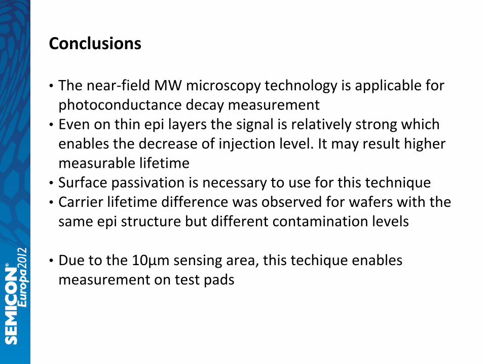
Conclusions
• The near-field MW microscopy technology is applicable for photoconductance decay measurement
• Even on thin epi layers the signal is relatively strong which enables the decrease of injection level. It may result higher measurable lifetime
• Surface passivation is necessary to use for this technique • Carrier lifetime difference was observed for wafers with the
same epi structure but different contamination levels
• Due to the 10µm sensing area, this techique enables measurement on test pads