Embed Size (px)
Citation preview
Supported by:
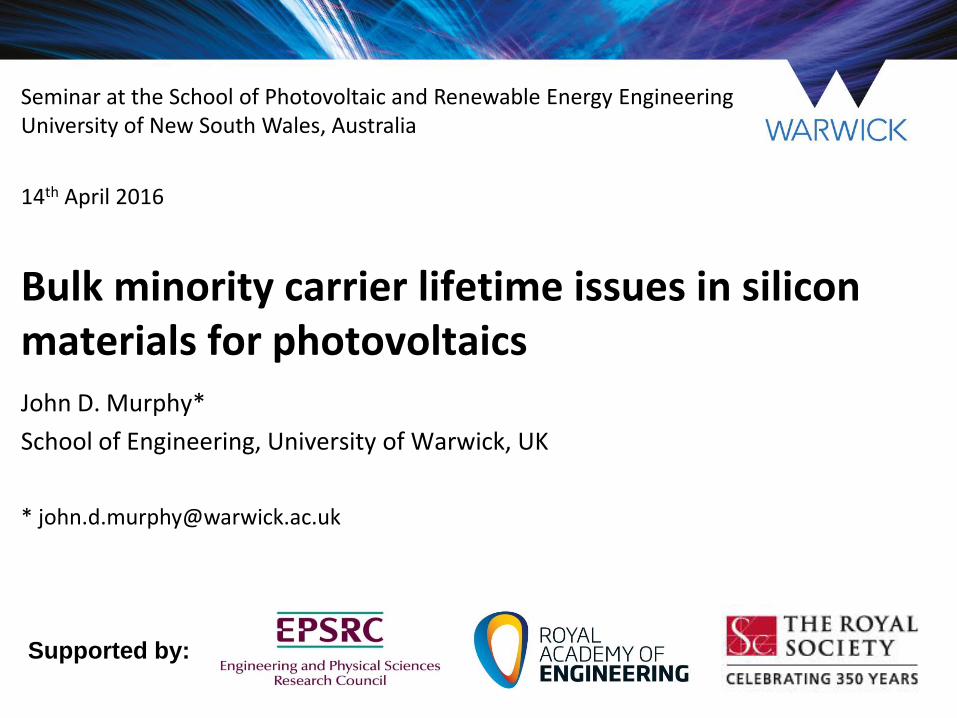
John D. Murphy*
School of Engineering, University of Warwick, UK
Bulk minority carrier lifetime issues in silicon materials for photovoltaics
14th April 2016
Seminar at the School of Photovoltaic and Renewable Energy Engineering University of New South Wales, Australia
2
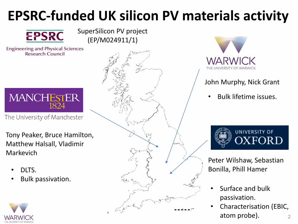
EPSRC-funded UK silicon PV materials activity
John Murphy, Nick Grant
Tony Peaker, Bruce Hamilton, Matthew Halsall, Vladimir Markevich
Peter Wilshaw, Sebastian Bonilla, Phill Hamer
• Surface and bulk passivation.
• Characterisation (EBIC, atom probe).
• Bulk lifetime issues.
• DLTS.• Bulk passivation.
SuperSilicon PV project(EP/M024911/1)
3
Bulk lifetime issues in PV
• Motivation for working on (silicon) PV is clear.
• Recent advances in surface passivation mean that bulk lifetime can limit the efficiency of some of the best cells.
• There is a need to understand the physics of the recombination process which occur in PV substrates.
• Need to be able to quantify lifetime and study it during cell processing, and ideally need to develop processes to improve it.
4
Outline of talk
1. Injection-dependent lifetime analysis approach
2. Recombination at oxygen-related extended defects
3. Internal gettering in mc-Si
4. High lifetime silicon materials (if time allows)
5
Co-workers for this talk
• Robert Falster, Vladimir Voronkov
• Karsten Bothe, Rafael Krain
• Mohammad Al-Amin, Alex Pointon, Nick Grant
• Rachel McGuire
• Dan Macdonald, Fiacre Rougieux
6
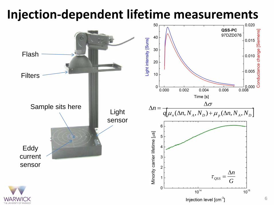
Injection-dependent lifetime measurements
Flash
Eddy
current
sensor
Filters
Sample sits hereLight
sensor
G
nQSS
DApDAn NNnNNnqn
,,(),,(
7
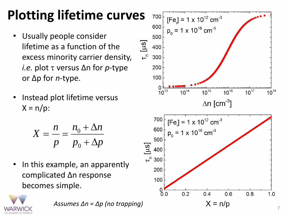
• Usually people consider lifetime as a function of the excess minority carrier density, i.e. plot versus Δn for p-type or Δp for n-type.
Plotting lifetime curves
• Instead plot lifetime versus X = n/p:
pp
nn
p
nX
0
0
• In this example, an apparently complicated Δn response becomes simple.
Assumes Δn = Δp (no trapping)
8
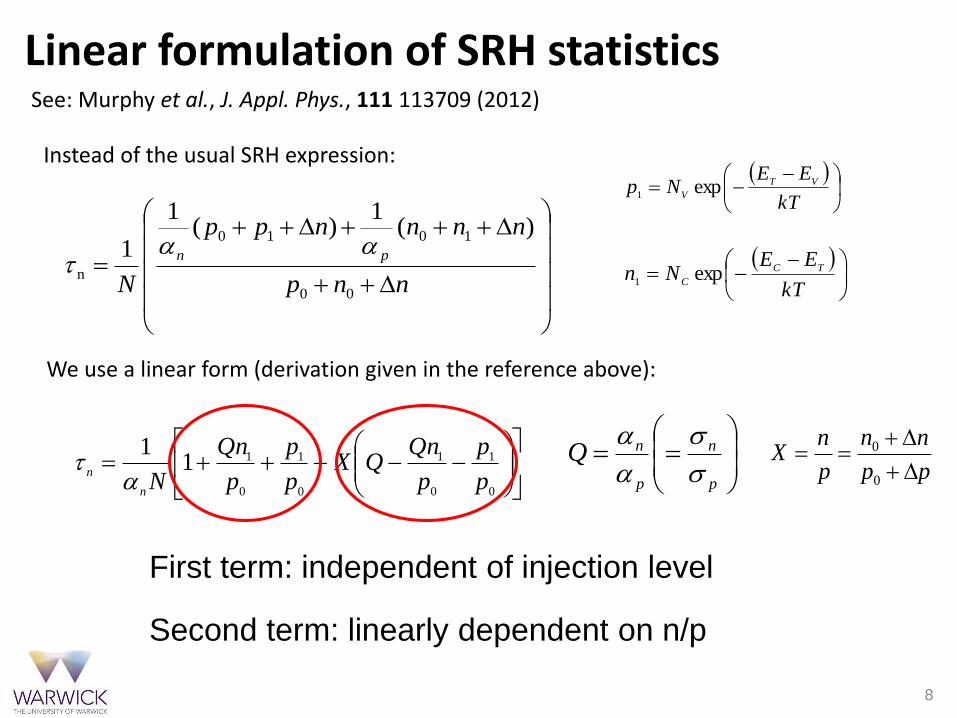
Linear formulation of SRH statisticsSee: Murphy et al., J. Appl. Phys., 111 113709 (2012)
0
1
0
1
0
1
0
111
p
p
p
QnQX
p
p
p
Qn
Nn
n
p
n
p
nQ
kT
EENn TC
Cexp
1
kT
EENp VT
Vexp
1
pp
nn
p
nX
0
0
nnp
nnnnpp
N
pn
00
1010
n
)(1
)(1
1
Second term: linearly dependent on n/p
First term: independent of injection level
Instead of the usual SRH expression:
We use a linear form (derivation given in the reference above):
9
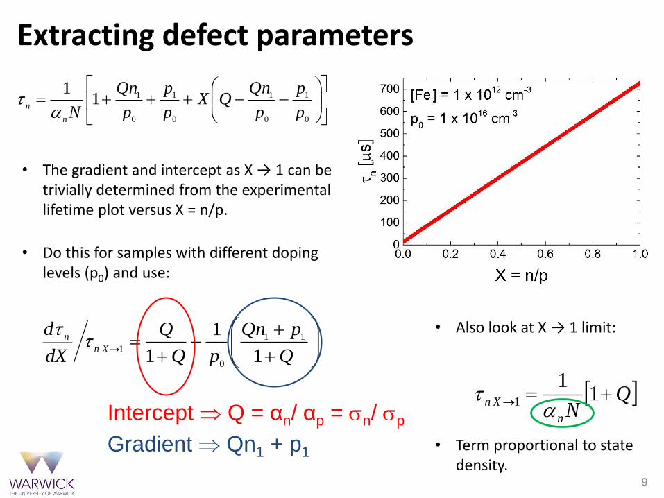
Extracting defect parameters
Q
pQn
pQ
Q
dX
dXn
n
1
1
1
11
0
1
0
1
0
1
0
1
0
111
p
p
p
QnQX
p
p
p
Qn
Nn
n
Intercept Q = αn/ αp = n/ p
Gradient Qn1 + p1
• The gradient and intercept as X → 1 can be trivially determined from the experimental lifetime plot versus X = n/p.
• Do this for samples with different doping levels (p0) and use:
• Also look at X → 1 limit:
QNn
Xn 11
1
• Term proportional to state density.
10
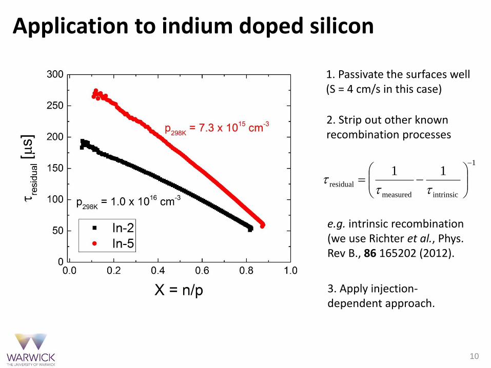
Application to indium doped silicon
1
intrinsicmeasured
residual
11
1. Passivate the surfaces well (S = 4 cm/s in this case)
2. Strip out other known recombination processes
e.g. intrinsic recombination (we use Richter et al., Phys. Rev B., 86 165202 (2012).
3. Apply injection-dependent approach.
11
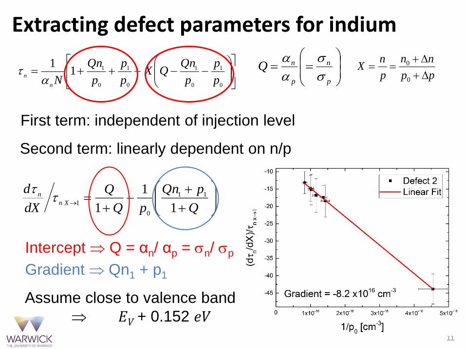
Extracting defect parameters for indium
0
1
0
1
0
1
0
111
p
p
p
QnQX
p
p
p
Qn
Nn
n
p
n
p
nQ
pp
nn
p
nX
0
0
Second term: linearly dependent on n/p
First term: independent of injection level
Q
pQn
pQ
Q
dX
dXn
n
1
1
1
11
0
1
Intercept Q = αn/ αp = n/ p
Gradient Qn1 + p1
Assume close to valence band
𝐸𝑉 + 0.152 𝑒𝑉
12
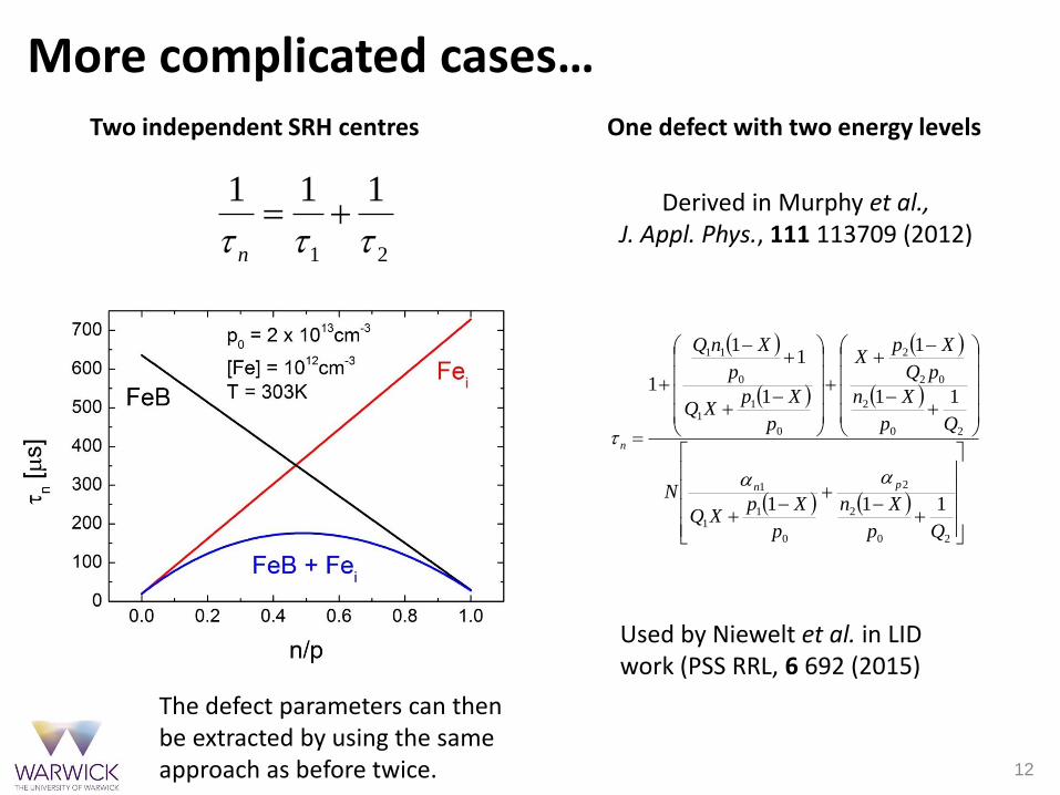
More complicated cases…Two independent SRH centres
20
2
2
0
11
1
20
2
02
2
0
11
0
11
111
11
1
1
11
1
Qp
Xn
p
XpXQ
N
Qp
Xn
pQ
XpX
p
XpXQ
p
XnQ
pn
n
One defect with two energy levels
Used by Niewelt et al. in LID work (PSS RRL, 6 692 (2015)
21
111
n
Derived in Murphy et al.,J. Appl. Phys., 111 113709 (2012)
The defect parameters can then be extracted by using the same approach as before twice.
13
Summary of the linear SRH approach
• The physics is the same as the “normal” approach, but the linear approach provides a neat way of visualising what is going on.
• Key points:
• A single lifetime measurement cannot tell you very much about the SRH properties of the defect.
• Varying with majority carrier concentration (doping level) easily allows information on the energy level and ratio of cross sections to be extracted if the samples are well controlled.
• Getting the state density in isolation from lifetime measurements is not possible as it is always multiplied by the capture coefficient (cross-section).
14
Outline of talk
1. Injection-dependent lifetime analysis approach
2. Recombination at oxygen-related extended defects
3. Internal gettering in mc-Si
4. High lifetime silicon materials
15
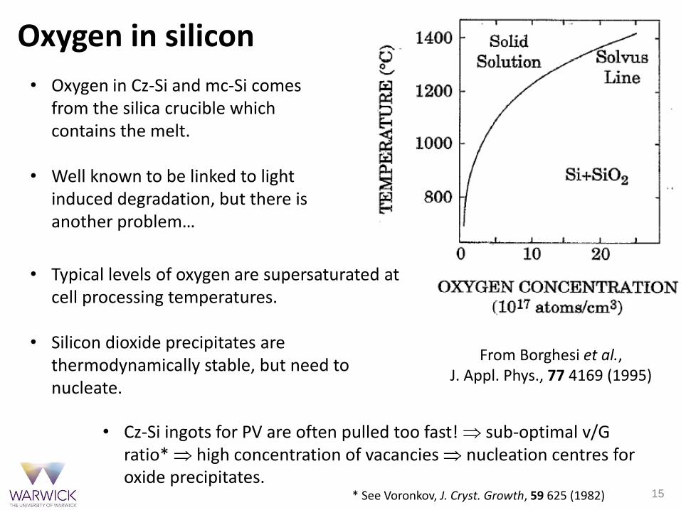
Oxygen in silicon
• Oxygen in Cz-Si and mc-Si comes from the silica crucible which contains the melt.
• Well known to be linked to light induced degradation, but there is another problem…
From Borghesi et al.,J. Appl. Phys., 77 4169 (1995)
• Typical levels of oxygen are supersaturated at cell processing temperatures.
• Silicon dioxide precipitates are thermodynamically stable, but need to nucleate.
• Cz-Si ingots for PV are often pulled too fast! sub-optimal v/G ratio* high concentration of vacancies nucleation centres for oxide precipitates.
* See Voronkov, J. Cryst. Growth, 59 625 (1982)
16
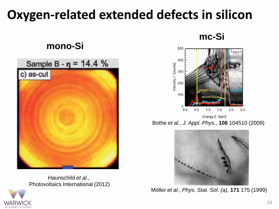
Oxygen-related extended defects in silicon
Haunschild et al.,
Photovoltaics International (2012)Möller et al., Phys. Stat. Sol. (a), 171 175 (1999)
mono-Simc-Si
Bothe et al., J. Appl. Phys., 106 104510 (2009)
17
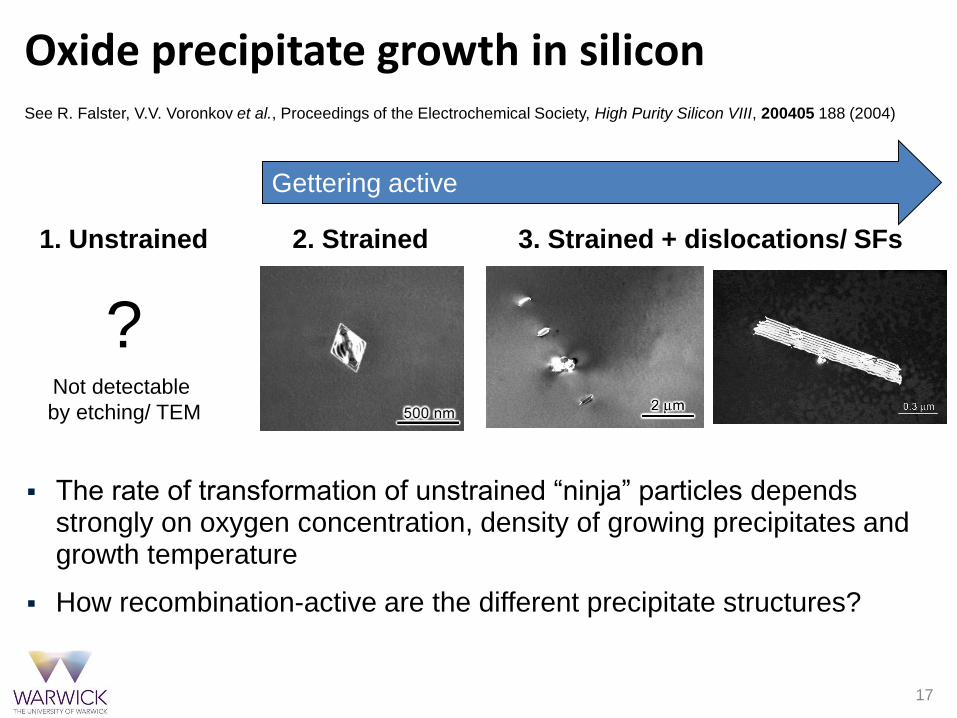
Oxide precipitate growth in siliconSee R. Falster, V.V. Voronkov et al., Proceedings of the Electrochemical Society, High Purity Silicon VIII, 200405 188 (2004)
1. Unstrained
?Not detectable
by etching/ TEM
2. Strained 3. Strained + dislocations/ SFs
Gettering active
The rate of transformation of unstrained “ninja” particles depends strongly on oxygen concentration, density of growing precipitates and growth temperature
How recombination-active are the different precipitate structures?
18
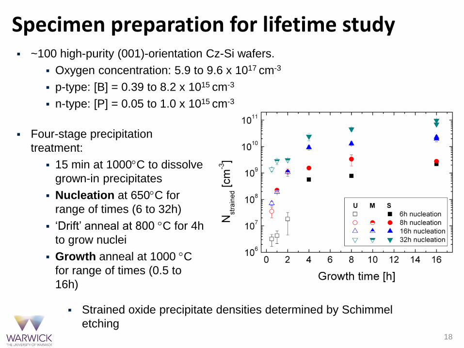
Specimen preparation for lifetime study ~100 high-purity (001)-orientation Cz-Si wafers.
Oxygen concentration: 5.9 to 9.6 x 1017 cm-3
p-type: [B] = 0.39 to 8.2 x 1015 cm-3
n-type: [P] = 0.05 to 1.0 x 1015 cm-3
Four-stage precipitation
treatment:
15 min at 1000C to dissolve
grown-in precipitates
Nucleation at 650C for
range of times (6 to 32h)
‘Drift’ anneal at 800 C for 4h
to grow nuclei
Growth anneal at 1000 C
for range of times (0.5 to
16h)
Strained oxide precipitate densities determined by Schimmel
etching
19
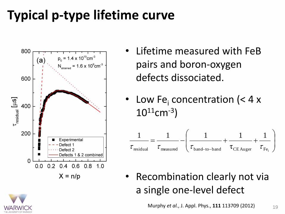
Typical p-type lifetime curve
• Lifetime measured with FeBpairs and boron-oxygen defects dissociated.
• Low Fei concentration (< 4 x 1011cm-3)
• Recombination clearly not via a single one-level defect
iFeAuger CEbandtobandmeasuredresidual
1
τ
1111
Murphy et al., J. Appl. Phys., 111 113709 (2012)
20
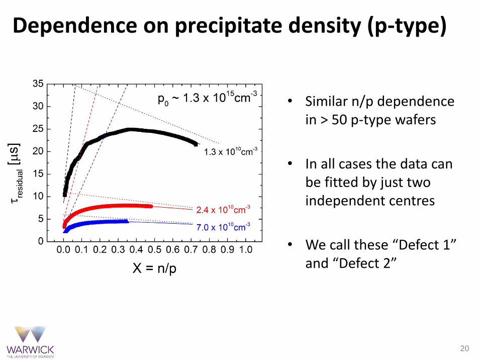
Dependence on precipitate density (p-type)
• Similar n/p dependence in > 50 p-type wafers
• In all cases the data can be fitted by just two independent centres
• We call these “Defect 1” and “Defect 2”
21
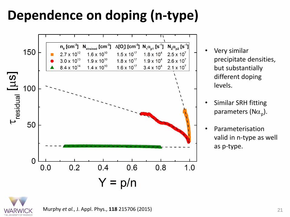
Dependence on doping (n-type)
• Very similar precipitate densities, but substantially different doping levels.
• Similar SRH fitting parameters (Np).
• Parameterisation valid in n-type as well as p-type.
Murphy et al., J. Appl. Phys., 118 215706 (2015)
22
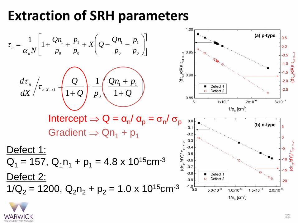
Extraction of SRH parameters
Q
pQn
pQ
Q
dX
dXn
n
1
1
1
11
0
1
0
1
0
1
0
1
0
111
p
p
p
QnQX
p
p
p
Qn
Nn
n
Intercept Q = αn/ αp = n/ p
Gradient Qn1 + p1
Defect 1:
Q1 = 157, Q1n1 + p1 = 4.8 x 1015cm-3
Defect 2:
1/Q2 = 1200, Q2n2 + p2 = 1.0 x 1015cm-3
23
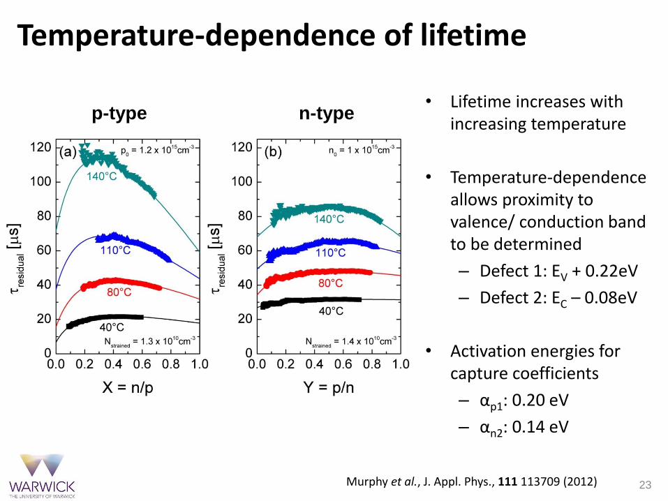
Temperature-dependence of lifetime
• Lifetime increases with increasing temperature
• Temperature-dependence allows proximity to valence/ conduction band to be determined
– Defect 1: EV + 0.22eV
– Defect 2: EC – 0.08eV
• Activation energies for capture coefficients
– αp1: 0.20 eV
– αn2: 0.14 eV
p-type n-type
Murphy et al., J. Appl. Phys., 111 113709 (2012)
24
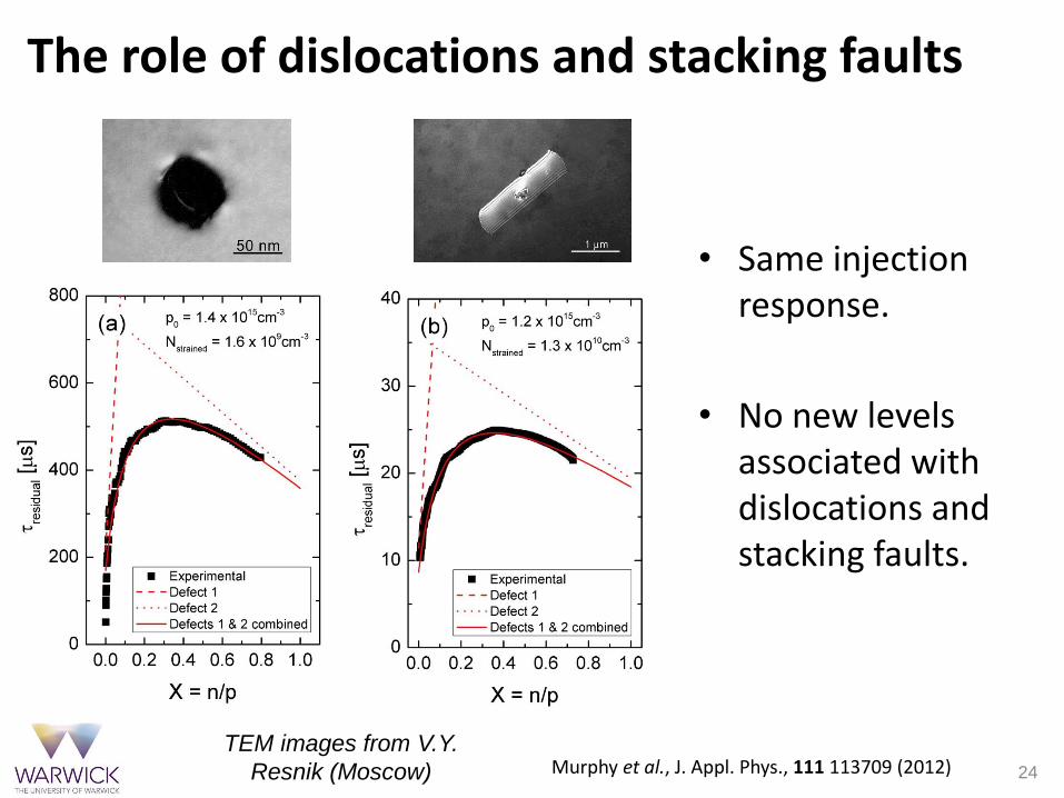
The role of dislocations and stacking faults
• Same injection response.
• No new levels associated with dislocations and stacking faults.
TEM images from V.Y.
Resnik (Moscow) Murphy et al., J. Appl. Phys., 111 113709 (2012)
25
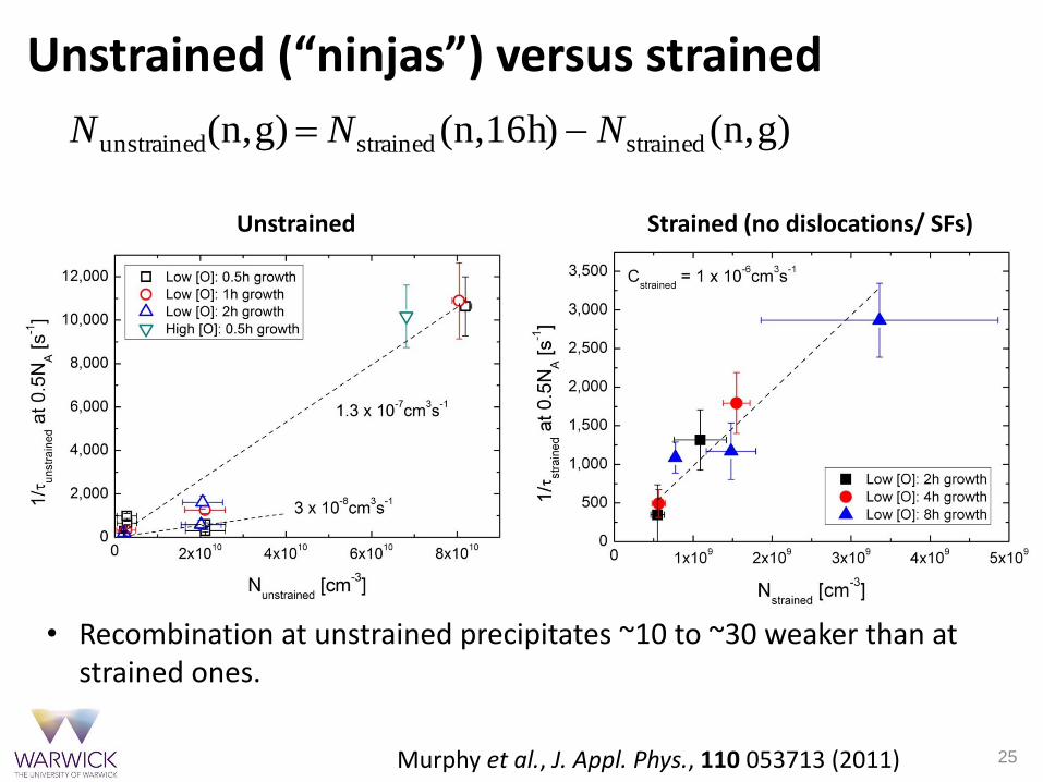
Unstrained (“ninjas”) versus strained
)gn,()16h n,()gn,( strainedstrainedunstrained NNN
Murphy et al., J. Appl. Phys., 110 053713 (2011)
Unstrained Strained (no dislocations/ SFs)
• Recombination at unstrained precipitates ~10 to ~30 weaker than at strained ones.
26
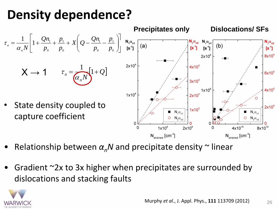
Density dependence?
0
1
0
1
0
1
0
111
p
p
p
QnQX
p
p
p
Qn
Nn
n
QNn
n 11
X → 1
• Relationship between αnN and precipitate density ~ linear
• Gradient ~2x to 3x higher when precipitates are surrounded by dislocations and stacking faults
Dislocations/ SFsPrecipitates only
• State density coupled to capture coefficient
Murphy et al., J. Appl. Phys., 111 113709 (2012)
27
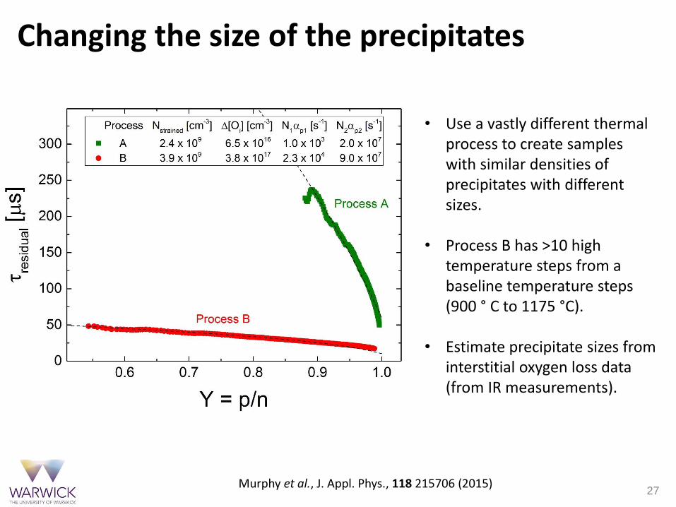
Changing the size of the precipitates
• Use a vastly different thermal process to create samples with similar densities of precipitates with different sizes.
• Process B has >10 high temperature steps from a baseline temperature steps (900 ° C to 1175 °C).
• Estimate precipitate sizes from interstitial oxygen loss data (from IR measurements).
Murphy et al., J. Appl. Phys., 118 215706 (2015)
28
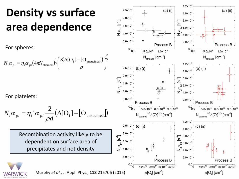
Density vs surface area dependence
unstrainedi O]O[2
' d
N piipii
3
2
unstrainedi3
1
strained
]O[]O[34
NN piipii
For spheres:
For platelets:
Recombination activity likely to be dependent on surface area of precipitates and not density
Murphy et al., J. Appl. Phys., 118 215706 (2015)
29
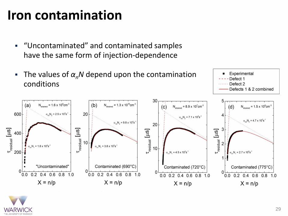
Iron contamination
“Uncontaminated” and contaminated samples have the same form of injection-dependence
The values of αnN depend upon the contamination conditions
30
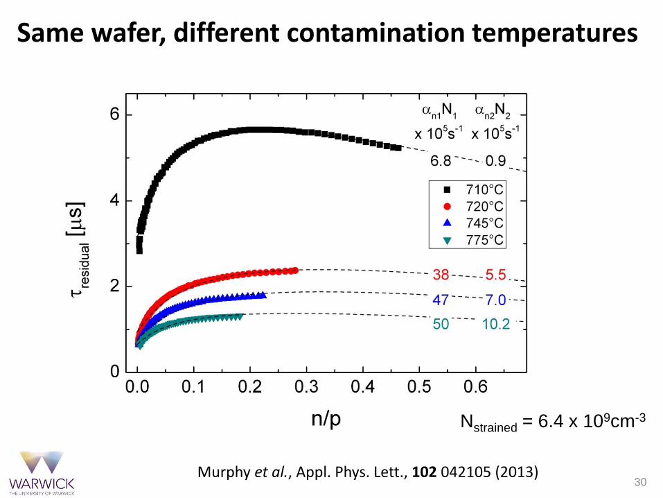
Same wafer, different contamination temperatures
Nstrained = 6.4 x 109cm-3
Murphy et al., Appl. Phys. Lett., 102 042105 (2013)
31
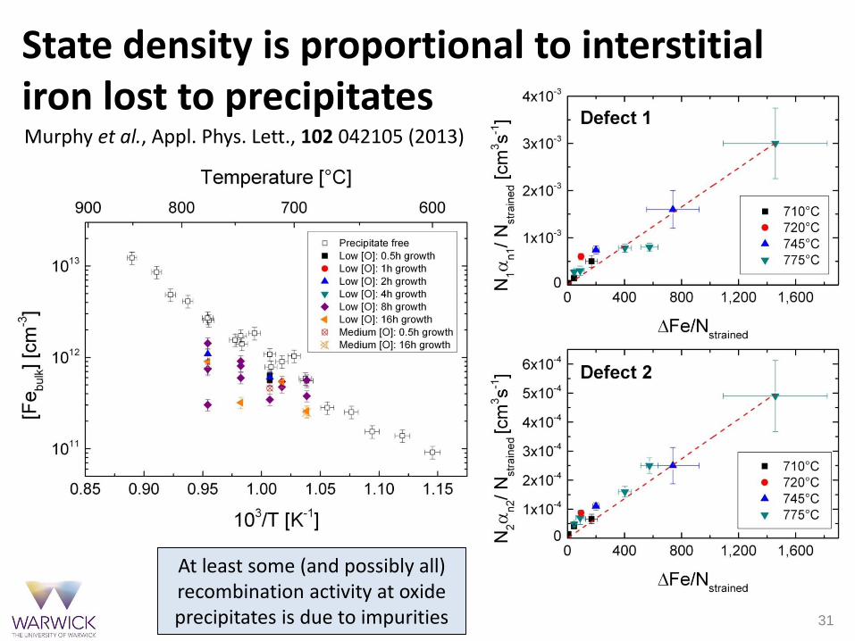
State density is proportional to interstitial iron lost to precipitates
At least some (and possibly all) recombination activity at oxide precipitates is due to impurities
Murphy et al., Appl. Phys. Lett., 102 042105 (2013)
32
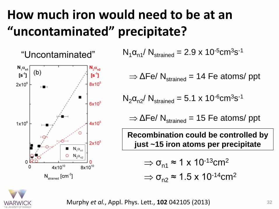
How much iron would need to be at an “uncontaminated” precipitate?
“Uncontaminated” N1αn1/ Nstrained = 2.9 x 10⁻⁵cm3s-1
N2αn2/ Nstrained = 5.1 x 10⁻⁶cm3s-1
ΔFe/ Nstrained = 14 Fe atoms/ ppt
ΔFe/ Nstrained = 15 Fe atoms/ ppt
Recombination could be controlled by
just ~15 iron atoms per precipitate
σn1 ≈ 1 x 10-13cm2
σn2 ≈ 1.5 x 10⁻¹⁴cm2
Murphy et al., Appl. Phys. Lett., 102 042105 (2013)
33
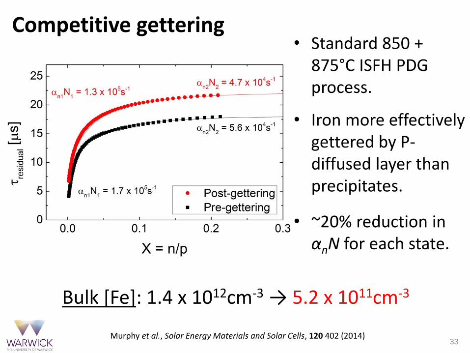
Competitive gettering• Standard 850 +
875°C ISFH PDG process.
• Iron more effectively gettered by P-diffused layer than precipitates.
• ~20% reduction in αnN for each state.
Bulk [Fe]: 1.4 x 1012cm-3 → 5.2 x 1011cm-3
Murphy et al., Solar Energy Materials and Solar Cells, 120 402 (2014)
34
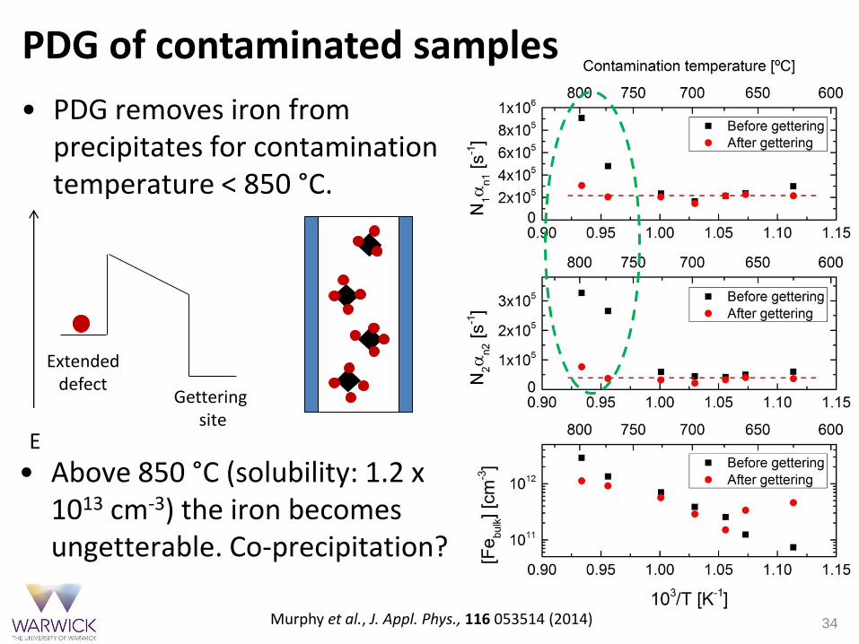
• X.
Murphy et al., J. Appl. Phys., 116 053514 (2014)
• PDG removes iron from precipitates for contamination temperature < 850 °C.
Extendeddefect
Getteringsite
E
• Above 850 °C (solubility: 1.2 x 1013 cm-3) the iron becomes ungetterable. Co-precipitation?
PDG of contaminated samples
35
Summary of Part II (oxide precipitates)
• Injection-dependent lifetime measurements on samples with different doping levels reveal two independent SRH centres:
• “Defect 1” at EV + 0.22eV, with Q1 = αn1/ αp1 = 157• “Defect 2” at EC – 0.08eV, 1/Q2 = αp2/ αn2 = 1,200
• In “uncontaminated” materials, the density of states is dependent on the total surface area of the precipitates (not density).
• Iron decorated oxide precipitates have the same centres with density being proportional to interstitial iron loss. Possible that all recombination activity is due to impurities.
• Reasonable levels of iron can be gettered away from oxide precipitates , although very high levels of iron at oxide precipitates is not getterable.
36
Outline of talk
1. Injection-dependent lifetime analysis approach
2. Recombination at oxygen-related extended defects
3. Internal gettering in mc-Si
4. High lifetime silicon materials
37
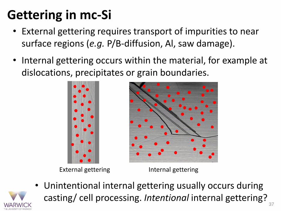
Gettering in mc-Si• External gettering requires transport of impurities to near
surface regions (e.g. P/B-diffusion, Al, saw damage).
• Internal gettering occurs within the material, for example at dislocations, precipitates or grain boundaries.
External gettering Internal gettering
• Unintentional internal gettering usually occurs during casting/ cell processing. Intentional internal gettering?
38
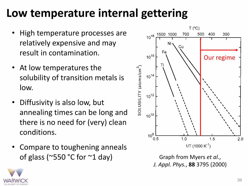
Low temperature internal gettering
• High temperature processes are relatively expensive and may result in contamination.
• At low temperatures the solubility of transition metals is low.
• Diffusivity is also low, but annealing times can be long and there is no need for (very) clean conditions.
• Compare to toughening anneals of glass (~550 °C for ~1 day)
Our regime
Graph from Myers et al.,J. Appl. Phys., 88 3795 (2000)
39
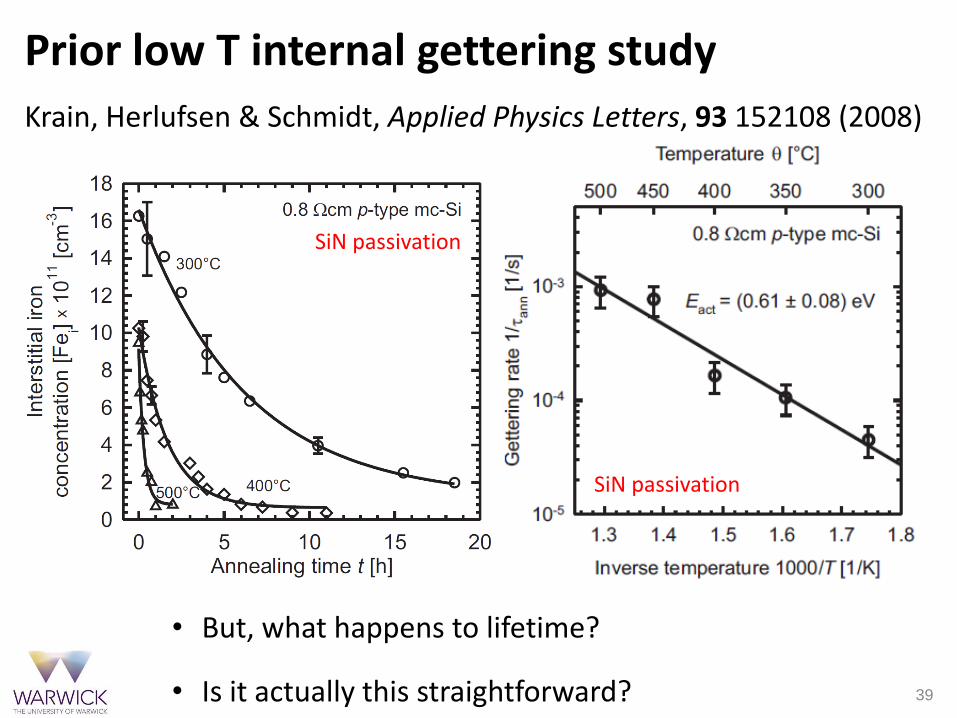
Prior low T internal gettering study
• But, what happens to lifetime?
• Is it actually this straightforward?
Krain, Herlufsen & Schmidt, Applied Physics Letters, 93 152108 (2008)
SiN passivation
SiN passivation
40
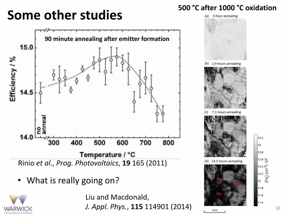
Some other studies
90 minute annealing after emitter formation
Rinio et al., Prog. Photovoltaics, 19 165 (2011)
500 °C after 1000 °C oxidation
Liu and Macdonald,J. Appl. Phys., 115 114901 (2014)
• What is really going on?
41
Studying internal gettering is difficult. Why?
1. Defect distribution changes during surface passivation.• Particularly for high temperature oxidations. • Also a problem at low temperatures (for SiN, Al2O3).
2. Surface passivation can introduce hydrogen.• This probably happens for SiN at 350 to 400 °C.• Difficult to distinguish between transport and bulk
passivation effects.
3. Annealing affects the surface recombination velocity.• Difficult to report a consistent bulk lifetime.
In our study we try to overcome the above issues in an attempt better to understand internal gettering in mc-Si.
42
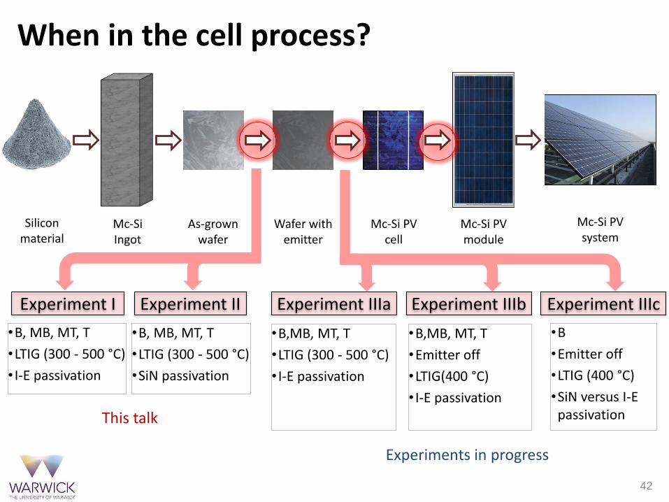
When in the cell process?
Experiment I
Siliconmaterial
Mc-SiIngot
As-grown wafer
Wafer with emitter
Mc-Si PV cell
Mc-Si PV module
Mc-Si PV system
•B, MB, MT, T
•LTIG (300 - 500 °C)
• I-E passivation
•B, MB, MT, T
•LTIG (300 - 500 °C)
•SiN passivation
•B,MB, MT, T
•LTIG (300 - 500 °C)
• I-E passivation
•B,MB, MT, T
•Emitter off
•LTIG(400 °C)
• I-E passivation
•B
•Emitter off
•LTIG (400 °C)
•SiN versus I-E passivation
Experiment II Experiment IIIa Experiment IIIb Experiment IIIc
Experiments in progress
This talk
43
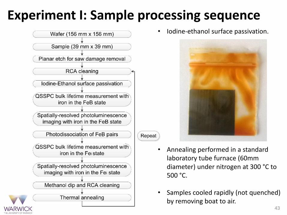
Experiment I: Sample processing sequence• Iodine-ethanol surface passivation.
• Annealing performed in a standard laboratory tube furnace (60mm diameter) under nitrogen at 300 °C to 500 °C.
• Samples cooled rapidly (not quenched) by removing boat to air.
44
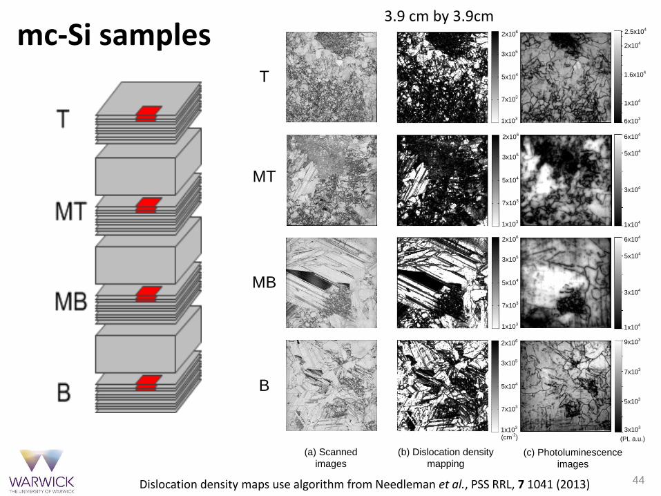
mc-Si samples
5x10⁴
7x10³
1x10³
3x10⁵
2x10⁶
5x10⁴
7x10³
1x10³
3x10⁵
2x10⁶
MB
B 5x10⁴
7x10³
1x10³
3x10⁵
2x10⁶
T
MT
5x10⁴
7x10³
1x10³
3x10⁵
2x10⁶
(cm-2
)3x10
3
5x10³
7x10³
9x10³
(PL a.u.)
1x10⁴
3x10⁴
5x10⁴
6x10⁴
1x10⁴
3x10⁴
5x10⁴
6x10⁴
6x10³
1x10⁴
2x10⁴
1.6x10⁴
2.5x10⁴
(a) Scanned
images
(b) Dislocation density
mapping (c) Photoluminescence
images
3.9 cm by 3.9cm
Dislocation density maps use algorithm from Needleman et al., PSS RRL, 7 1041 (2013)
45
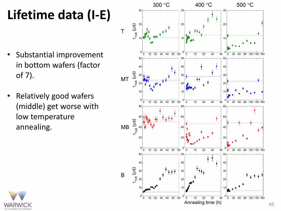
Lifetime data (I-E)
• Substantial improvement in bottom wafers (factor of 7).
• Relatively good wafers (middle) get worse with low temperature annealing.
46
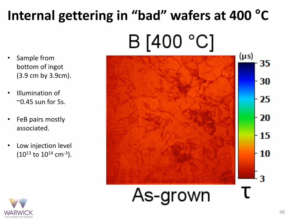
Internal gettering in “bad” wafers at 400 °C
• Sample from bottom of ingot (3.9 cm by 3.9cm).
• Illumination of ~0.45 sun for 5s.
• FeB pairs mostly associated.
• Low injection level (1013 to 1014 cm-3).
47
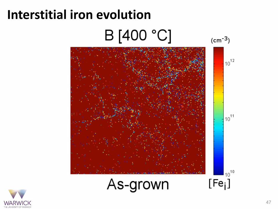
Interstitial iron evolution
48
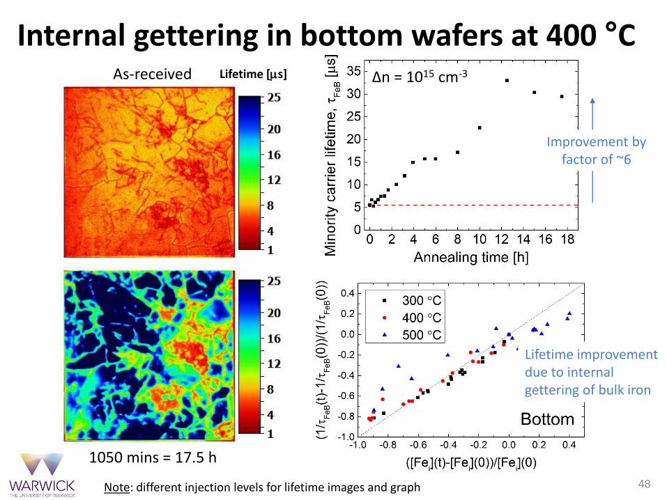
Internal gettering in bottom wafers at 400 °C
1050 mins = 17.5 h
As-received Lifetime [s]
Note: different injection levels for lifetime images and graph
Improvement by factor of ~6
Δn = 1015 cm-3
Lifetime improvement due to internal gettering of bulk iron
49
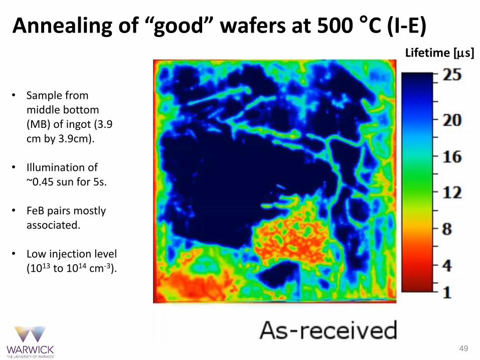
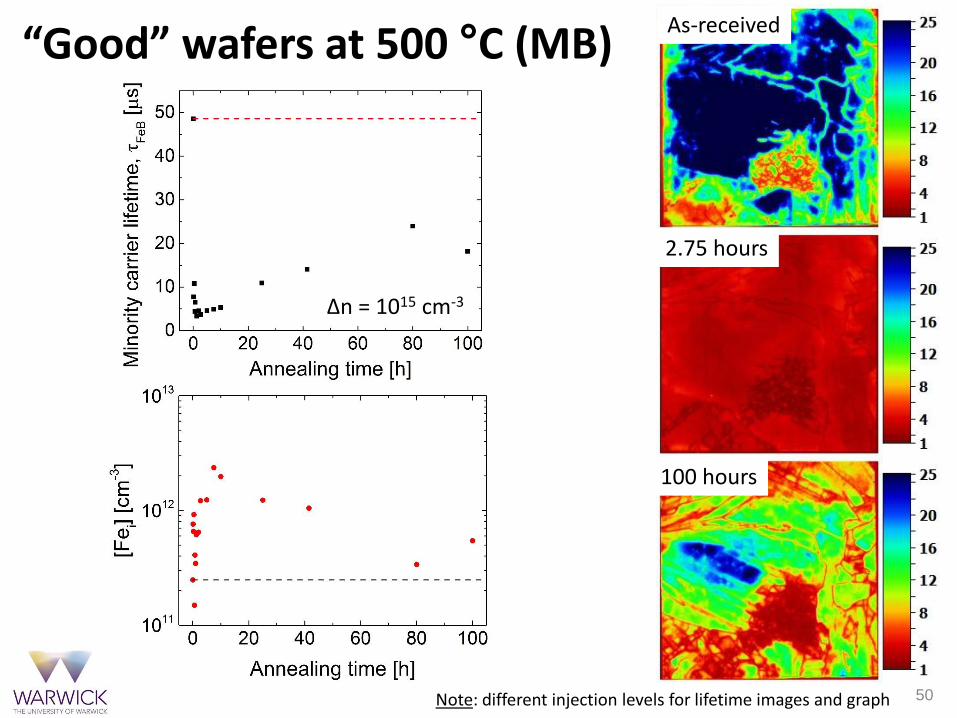
Annealing of “good” wafers at 500 °C (I-E)
• Sample from middle bottom (MB) of ingot (3.9 cm by 3.9cm).
• Illumination of ~0.45 sun for 5s.
• FeB pairs mostly associated.
• Low injection level (1013 to 1014 cm-3).
Lifetime [s]
50
“Good” wafers at 500 °C (MB)As-received
2.75 hours
100 hours
Δn = 1015 cm-3
Note: different injection levels for lifetime images and graph
51
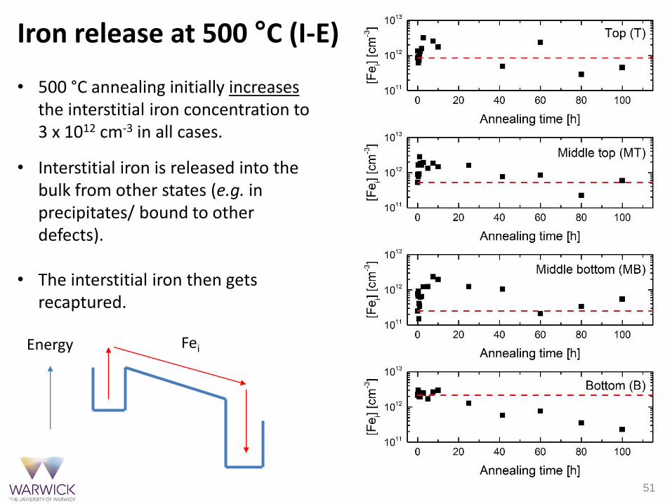
Iron release at 500 °C (I-E)
• 500 °C annealing initially increasesthe interstitial iron concentration to 3 x 1012 cm-3 in all cases.
• Interstitial iron is released into the bulk from other states (e.g. in precipitates/ bound to other defects).
• The interstitial iron then gets recaptured.
FeiEnergy
52
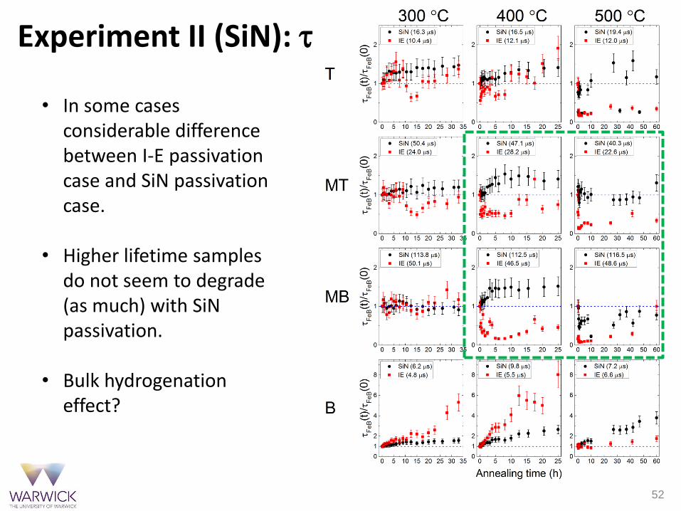
• In some cases considerable difference between I-E passivation case and SiN passivation case.
• Higher lifetime samples do not seem to degrade (as much) with SiNpassivation.
• Bulk hydrogenation effect?
Experiment II (SiN):
53
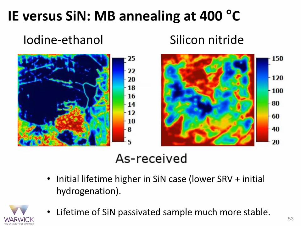
IE versus SiN: MB annealing at 400 °C
Iodine-ethanol Silicon nitride
• Initial lifetime higher in SiN case (lower SRV + initial hydrogenation).
• Lifetime of SiN passivated sample much more stable.
54
• In some cases considerable difference between I-E passivation case and SiNpassivation case.
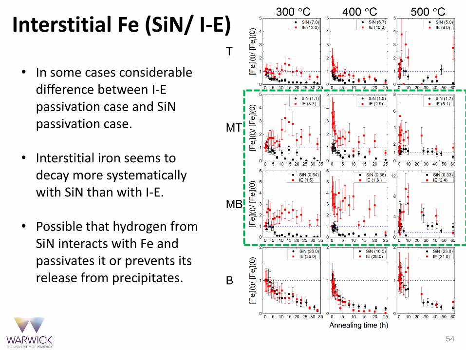
• Interstitial iron seems to decay more systematically with SiN than with I-E.
• Possible that hydrogen from SiN interacts with Fe and passivates it or prevents its release from precipitates.
Interstitial Fe (SiN/ I-E)
55
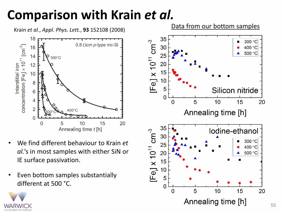
Comparison with Krain et al.Krain et al., Appl. Phys. Lett., 93 152108 (2008)
• We find different behaviour to Krain et al.’s in most samples with either SiN or IE surface passivation.
• Even bottom samples substantially different at 500 °C.
Data from our bottom samples
56
Summary – low temperature annealing
• Low temperature annealing can improve the carrier lifetime of as-received mc-Si in certain cases and hydrogen is not necessary for the effect to occur.
• Low lifetime bottom wafers are always improved (with and without hydrogen) by gettering of iron. Lifetime can improve by a factor of > 6 (so far) by annealing for 10+ hours at 400 °C.
• Low lifetime top wafers are not significantly improved by low temperature annealing.
• Good wafers from the middle are not improved. Iron release into the bulk at 400 °C and 500 °C appears to be prevented by hydrogenation.
• The behaviour of iron in silicon at 300 °C to 500 °C is a complicated problem and needs further investigation.
57
Outline of talk
1. Injection-dependent lifetime analysis approach
2. Recombination at oxygen-related extended defects
3. Internal gettering in mc-Si
4. High lifetime silicon materials
58
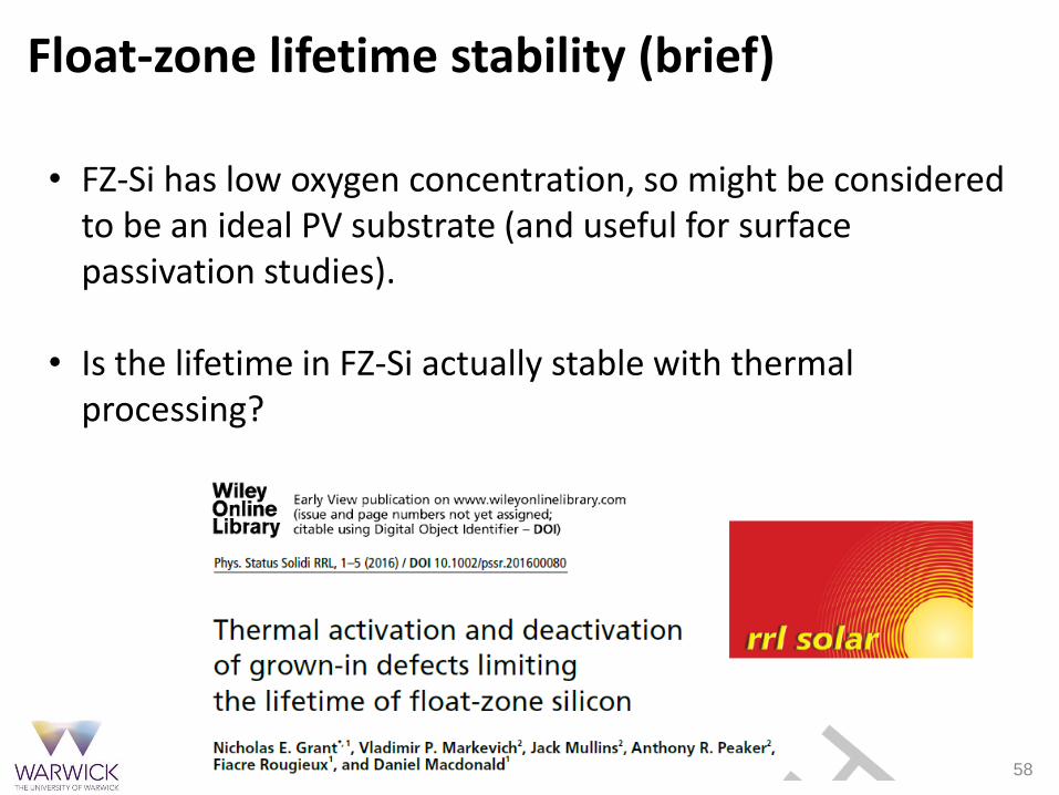
Float-zone lifetime stability (brief)
• FZ-Si has low oxygen concentration, so might be considered to be an ideal PV substrate (and useful for surface passivation studies).
• Is the lifetime in FZ-Si actually stable with thermal processing?
59
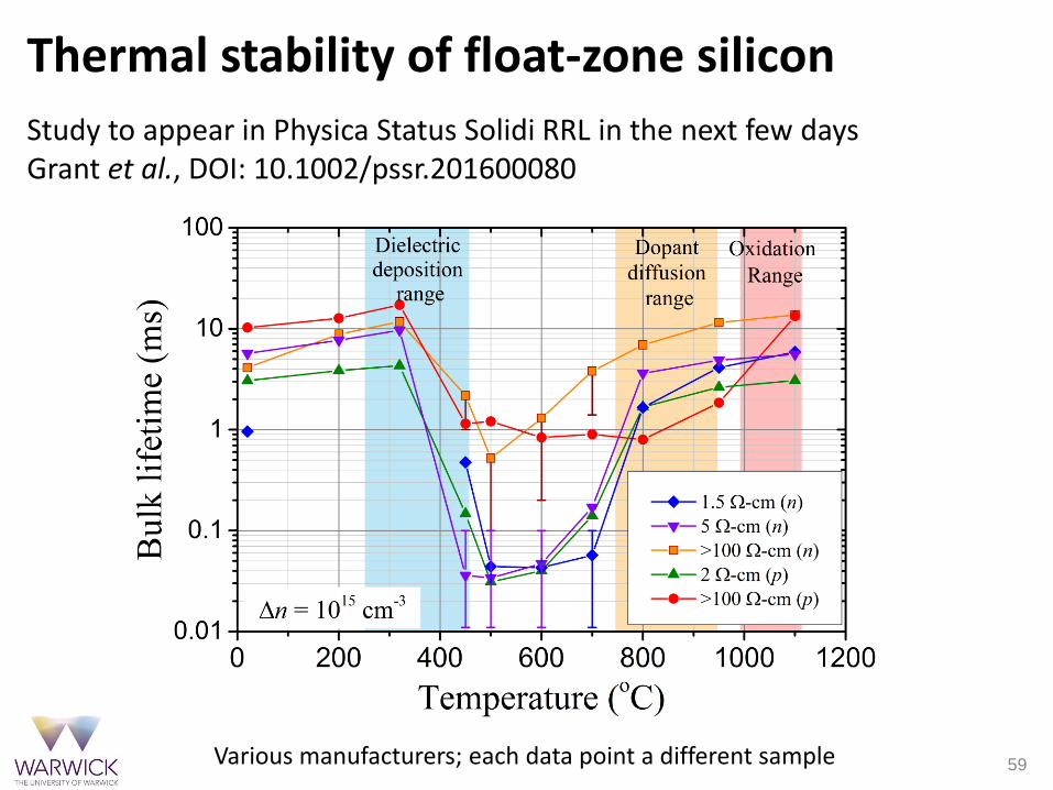
Thermal stability of float-zone silicon
Study to appear in Physica Status Solidi RRL in the next few daysGrant et al., DOI: 10.1002/pssr.201600080
Various manufacturers; each data point a different sample
60
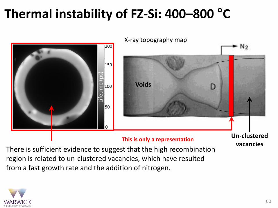
Thermal instability of FZ-Si: 400–800 °C
X-ray topography map
Voids
Un-clustered vacancies
There is sufficient evidence to suggest that the high recombination region is related to un-clustered vacancies, which have resulted from a fast growth rate and the addition of nitrogen.
This is only a representation
Life
tim
e (µ
s)
61
Overall summary
• Analysing the injection dependence of lifetime in terms of SRH statistics is relatively straightforward in well-controlled samples(have samples with different doping levels).
• Oxygen-related extended defects cause substantial lifetime reductions. Impurities at precipitates enhance recombination, but can be gettered away to an extent.
• Low temperature internal gettering can result in substantial improvements in lifetime in mc-Si, but the process is complicated.
• Passivation choice strongly affects low temperature annealing behaviour. Hydrogen appears to affect behaviour of iron.
• Any questions?