Embed Size (px)
Citation preview
www.ti.com
FEATURES DESCRIPTION
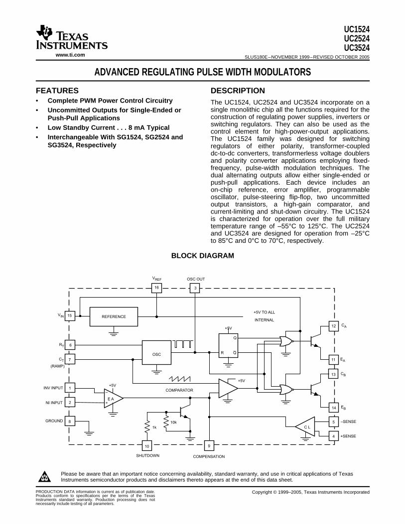
BLOCK DIAGRAM
15
7
6
16
VIN REFERENCE
VREF
+5V TO ALL
INTERNAL
RT
CT
OSC
(RAMP)
3
OSC OUT
Q
QR
+5V12
11
CA
EA
13
14
CB
EB
9
+5V
5
4
–SENSE
+SENSE
C L
COMPENSATION
10k
1k
10
8GROUND
+
–
+5V
E A
1
2
INV INPUT
NI INPUT
COMPARATOR
SHUTDOWN
UC1524UC2524UC3524
SLUS180E–NOVEMBER 1999–REVISED OCTOBER 2005
ADVANCED REGULATING PULSE WIDTH MODULATORS
• Complete PWM Power Control Circuitry The UC1524, UC2524 and UC3524 incorporate on asingle monolithic chip all the functions required for the• Uncommitted Outputs for Single-Ended orconstruction of regulating power supplies, inverters orPush-Pull Applicationsswitching regulators. They can also be used as the• Low Standby Current . . . 8 mA Typicalcontrol element for high-power-output applications.
• Interchangeable With SG1524, SG2524 and The UC1524 family was designed for switchingSG3524, Respectively regulators of either polarity, transformer-coupled
dc-to-dc converters, transformerless voltage doublersand polarity converter applications employing fixed-frequency, pulse-width modulation techniques. Thedual alternating outputs allow either single-ended orpush-pull applications. Each device includes anon-chip reference, error amplifier, programmableoscillator, pulse-steering flip-flop, two uncommittedoutput transistors, a high-gain comparator, andcurrent-limiting and shut-down circuitry. The UC1524is characterized for operation over the full militarytemperature range of –55°C to 125°C. The UC2524and UC3524 are designed for operation from –25°Cto 85°C and 0°C to 70°C, respectively.
Please be aware that an important notice concerning availability, standard warranty, and use in critical applications of TexasInstruments semiconductor products and disclaimers thereto appears at the end of this data sheet.
PRODUCTION DATA information is current as of publication date. Copyright © 1999–2005, Texas Instruments IncorporatedProducts conform to specifications per the terms of the TexasInstruments standard warranty. Production processing does notnecessarily include testing of all parameters.
www.ti.com
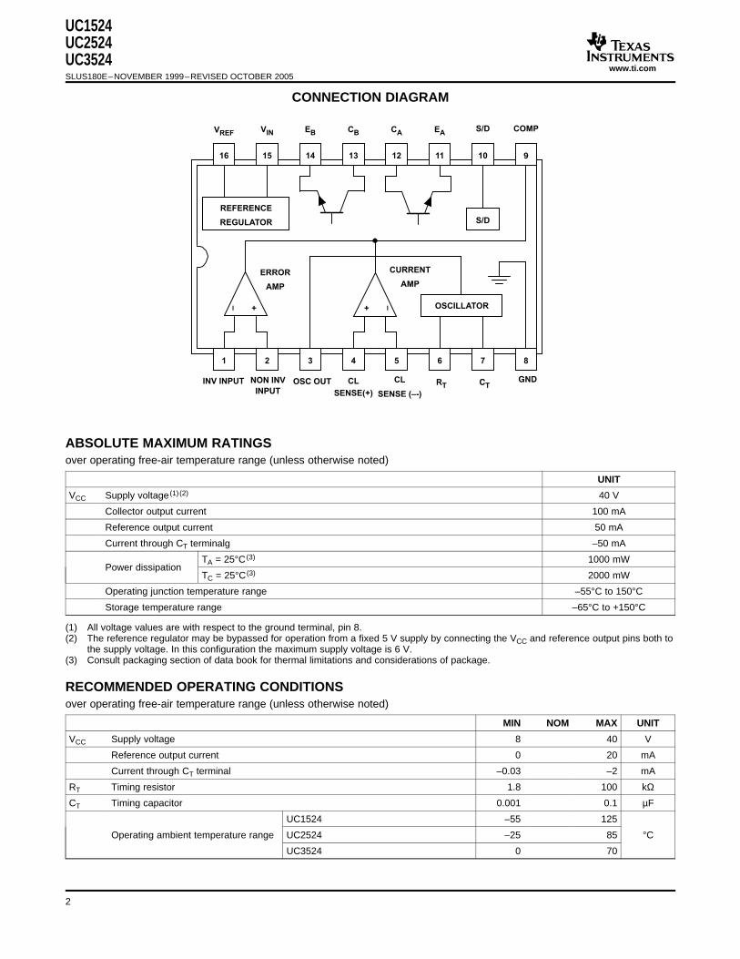
CONNECTION DIAGRAM
+–
+ –
OSCILLATOR
S/D
REFERENCE
REGULATOR
1 2 3 4 5 6 7 8
16 15 14 13 12 11 10 9
ERROR
AMP
CURRENT
AMP
VREF VIN EB CB CA EAS/D COMP
INV INPUT NON INV
INPUT
OSC OUT CL
SENSE(+)
CL
SENSE (–-)
RTGNDC
T
ABSOLUTE MAXIMUM RATINGS
RECOMMENDED OPERATING CONDITIONS
UC1524UC2524UC3524SLUS180E–NOVEMBER 1999–REVISED OCTOBER 2005
over operating free-air temperature range (unless otherwise noted)
UNIT
VCC Supply voltage (1) (2) 40 V
Collector output current 100 mA
Reference output current 50 mA
Current through CT terminalg –50 mA
TA = 25°C (3) 1000 mWPower dissipation
TC = 25°C (3) 2000 mW
Operating junction temperature range –55°C to 150°C
Storage temperature range –65°C to +150°C
(1) All voltage values are with respect to the ground terminal, pin 8.(2) The reference regulator may be bypassed for operation from a fixed 5 V supply by connecting the VCC and reference output pins both to
the supply voltage. In this configuration the maximum supply voltage is 6 V.(3) Consult packaging section of data book for thermal limitations and considerations of package.
over operating free-air temperature range (unless otherwise noted)
MIN NOM MAX UNIT
VCC Supply voltage 8 40 V
Reference output current 0 20 mA
Current through CT terminal –0.03 –2 mA
RT Timing resistor 1.8 100 kΩ
CT Timing capacitor 0.001 0.1 µF
UC1524 –55 125
Operating ambient temperature range UC2524 –25 85 °C
UC3524 0 70
2
www.ti.com
ELECTRICAL CHARACTERISTICS
UC1524UC2524UC3524
SLUS180E–NOVEMBER 1999–REVISED OCTOBER 2005
these specifications apply for TA = –55°C to 125°C for the UC1524, –25°C to 85°C for the UC2524, and 0°C to 70°C for theUC3524, VIN = 20 V, and f = 20 kHz, TA = TJ, over operating free-air temperature range (unless otherwise noted)
UC1524/UC2524 UC3524PARAMETER TEST CONDITIONS UNIT
MIN TYP MAX MIN TYP MAX
REFERENCE SECTION
Output voltage 4.8 5.0 5.2 4.6 5.0 5.4 V
Line regulation VIN = 8 V to 40 V 10 20 10 30 mV
Load regulation IL = 0 mA to 20 mA 20 50 20 50 mV
Ripple rejection f = 120 Hz, TJ = 25°C 66 66 dB
Short circuit current limit VREF = 0, TJ = 25°C 100 100 mA
Temperature stability Over operating temperature range 0.3% 1% 0.3% 1%
Long term stability TJ = 125°C, t = 1000 Hrs 20 20 mV
OSCILLATOR SECTION
Maximum frequency CT = 1 nF, RT = 2 kΩ 300 300 kHz
Initial accuracy RT and CT constant 5% 5%
Voltage stability VIN = 8 V to 40 V, TJ = 25°C 1% 1%
Temperature stability Over operating temperature range 5% 5%
Output amplitude Pin 3, TJ = 25°C 3.5 3.5 V
Output pulse width CT = 0.01 mfd, TJ = 25°C 0.5 0.5 µs
ERROR AMPLIFIER SECTION
Input offset voltage VCM = 2.5 V 0.5 5 2 10 mV
Input bias current VCM = 2.5 V 2 10 2 10 µA
Open loop voltage gain 72 80 60 80 dB
Common mode voltage TJ = 25°C 1.8 3.4 1.8 3.4 V
Common mode rejection ratio TJ = 25°C 70 70 dB
Small signal bandwidth AV = 0 dB, TJ = 25°C 3 3 MHz
Output voltage TJ = 25°C 0.5 3.8 0.5 3.8 V
COMPARATOR SECTION
Duty-cycle % Each output on 0% 45% 0% 45%
Zero duty-cycle 1 1Input threshold V
Maximum duty-cycle 3.5 3.5
Input bias current 1 1 µA
CURRENT LIMITING SECTION
Sense voltage Pin 9 = 2 V with error amplifier set for 190 200 210 180 200 220 mVmaximum out, TJ = 25°C
Sense voltage T.C. 0.2 0.2 mV/°C
TJ = –55°C to 85°C for the –1 V to 1 V limit –1 1 –1 1Common mode voltage V
TJ = 25°C –0.3 1
OUTPUT SECTION (EACH OUTPUT)
Collector-emitter voltage 40 40 V
Collector leakage current VCE = 40 V 0.1 50 0.1 50 µ A
Saturation voltage IC = 50 mA 1 2 1 2 V
Emitter output voltage VIN = 20 V 17 18 17 18 V
Rise Time RC = 2 kΩ, TJ = 25°C 0.2 0.2 µs
Fall Time RC = 2 kΩ, TJ = 25°C 0.1 0.1 µs
Total standby current (Note) VIN = 40 V 8 10 8 10 mA
3
www.ti.com
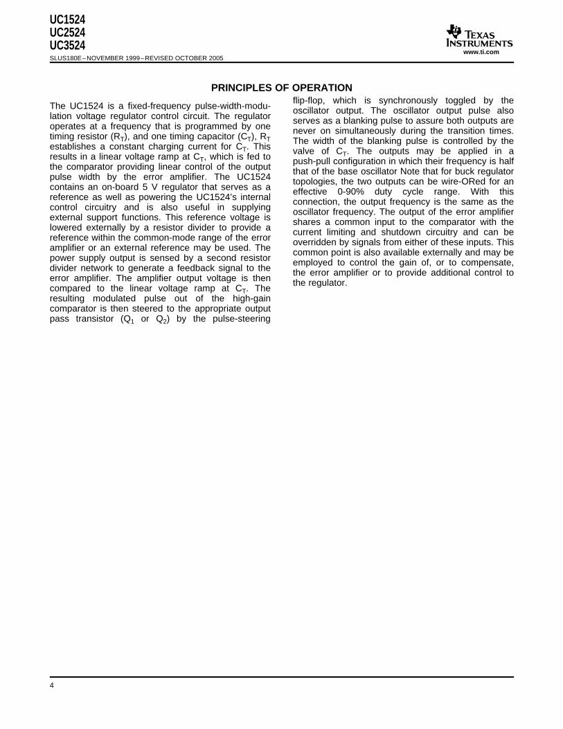
PRINCIPLES OF OPERATION
UC1524UC2524UC3524SLUS180E–NOVEMBER 1999–REVISED OCTOBER 2005
flip-flop, which is synchronously toggled by theThe UC1524 is a fixed-frequency pulse-width-modu- oscillator output. The oscillator output pulse alsolation voltage regulator control circuit. The regulator serves as a blanking pulse to assure both outputs areoperates at a frequency that is programmed by one never on simultaneously during the transition times.timing resistor (RT), and one timing capacitor (CT), RT The width of the blanking pulse is controlled by theestablishes a constant charging current for CT. This valve of CT. The outputs may be applied in aresults in a linear voltage ramp at CT, which is fed to push-pull configuration in which their frequency is halfthe comparator providing linear control of the output that of the base oscillator Note that for buck regulatorpulse width by the error amplifier. The UC1524 topologies, the two outputs can be wire-ORed for ancontains an on-board 5 V regulator that serves as a effective 0-90% duty cycle range. With thisreference as well as powering the UC1524’s internal connection, the output frequency is the same as thecontrol circuitry and is also useful in supplying oscillator frequency. The output of the error amplifierexternal support functions. This reference voltage is shares a common input to the comparator with thelowered externally by a resistor divider to provide a current limiting and shutdown circuitry and can bereference within the common-mode range of the error overridden by signals from either of these inputs. Thisamplifier or an external reference may be used. The common point is also available externally and may bepower supply output is sensed by a second resistor employed to control the gain of, or to compensate,divider network to generate a feedback signal to the the error amplifier or to provide additional control toerror amplifier. The amplifier output voltage is then the regulator.compared to the linear voltage ramp at CT. Theresulting modulated pulse out of the high-gaincomparator is then steered to the appropriate outputpass transistor (Q1 or Q2) by the pulse-steering
4
www.ti.com
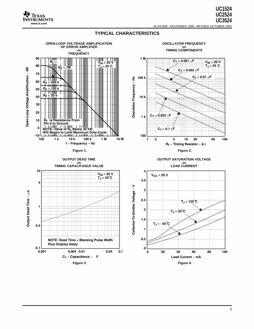
TYPICAL CHARACTERISTICS
40
30
10
−10100 1 k 10 k 100 k
Op
en
-Lo
op
Vo
lta
ge
Am
pli
fic
ati
on
−d
B
60
70
f − Frequency − Hz
90
1 M 10 M
0
20
50
80
RF = VIN = 20 VTJ = 25 CRF = 1M
RF = 300 k
RF = 100 k
RF = 30 k
RF is Resistance FromPin 9 to Ground
NOTE: Value of RF Below 30 kWWill Began to Limit Maximum Duty-Cycle
10 k
1 k
1001 2 5 10 20
Os
sc
ila
tor
Fre
qu
en
cy
−H
z 100 k
1 M
50 100
RT − Timing Resistor − kW
VIN = 20 VTJ = 25 C
CT = 0.001 mF
CT = 0.003 mF
CT = 0.01 mF
CT = 0.003 mF
CT = 0.1 mF
1
0.4
0.10.001 0.004 0.01
Ou
tpu
t D
ea
d T
ime
−
4
10
0.04 0.1
µs
CT − Capacitance − F
VIN = 20 VTJ = 25 C
NOTE: Dead Time = Blanking Pulse Width
Plus Outplay Delay
2
1.5
0.5
00 20 40 60
Co
lle
cto
r-T
o-E
mit
ter
Vo
lta
ge
−V
2.5
3.5
Load Current − mA
4
80 100
1
3
VCC = 20 V
TJ = 125 C
TJ = 25 C
TJ = −55 C
UC1524UC2524UC3524
SLUS180E–NOVEMBER 1999–REVISED OCTOBER 2005
OPEN-LOOP VOLTRAGE AMPLIFICATION OSCILLATOR FREQUENCYOF ERROR AMPLIFIER vs
vs TIMING COMPONENTSFREQUENCY
Figure 1. Figure 2.
OUTPUT DEAD TIME OUTPUT SATURATION VOLTAGEvs vs
TIMING CAPACITANCE VALUE LOAD CURRENT
Figure 3. Figure 4.
5
www.ti.com
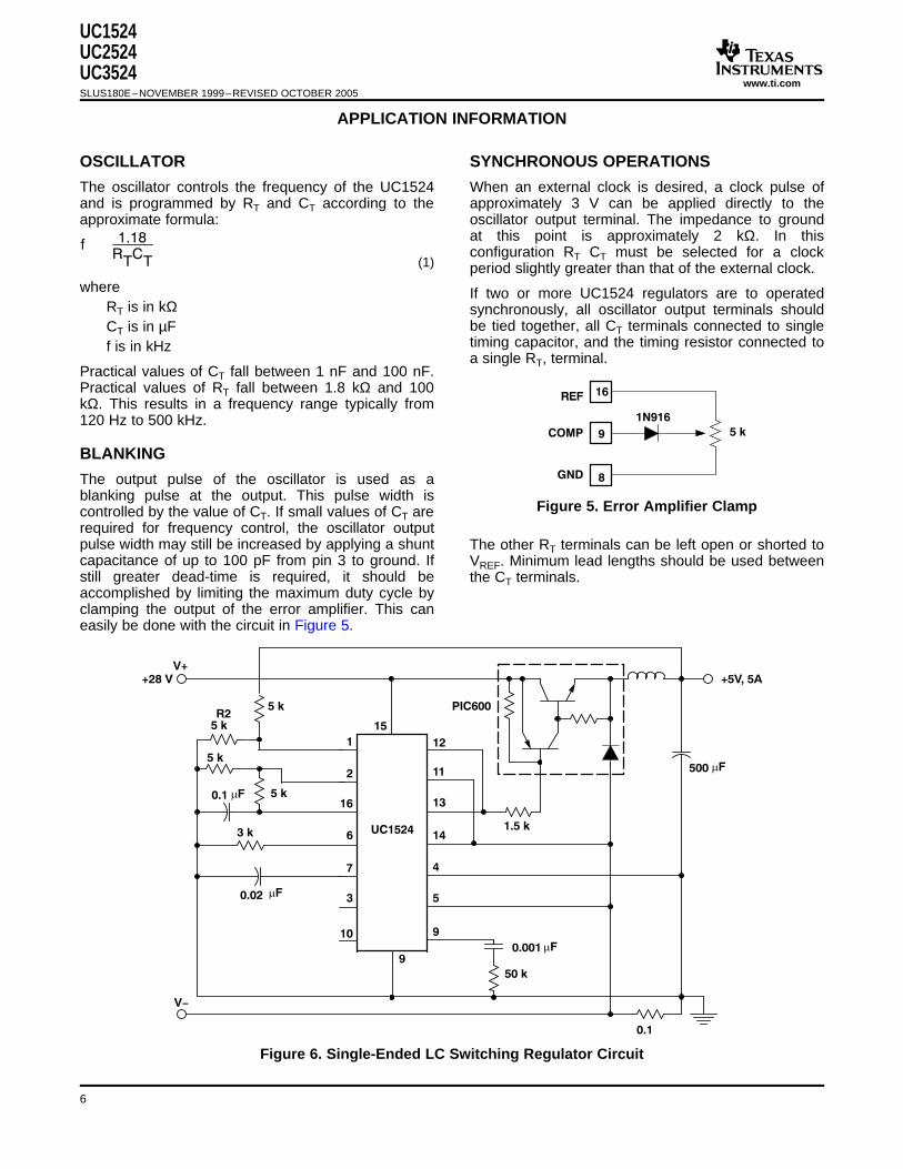
APPLICATION INFORMATION
OSCILLATOR SYNCHRONOUS OPERATIONS
f1.18
RT
CT (1)
BLANKING
REF
COMP 9
GND 8
1N916
16
5 k
V++28 V
V−
1
2
16
6
7
3
10
15
12
11
13
14
4
5
9
9
5 kR2
5 k
5 k
0.1 mF 5 k
3 k
0.02 mF
500 mF
1.5 k
0.001 mF
50 k
0.1
UC1524
PIC600
+5V, 5A
UC1524UC2524UC3524SLUS180E–NOVEMBER 1999–REVISED OCTOBER 2005
The oscillator controls the frequency of the UC1524 When an external clock is desired, a clock pulse ofand is programmed by RT and CT according to the approximately 3 V can be applied directly to theapproximate formula: oscillator output terminal. The impedance to ground
at this point is approximately 2 kΩ. In thisconfiguration RT CT must be selected for a clockperiod slightly greater than that of the external clock.
where If two or more UC1524 regulators are to operatedRT is in kΩ synchronously, all oscillator output terminals should
be tied together, all CT terminals connected to singleCT is in µFtiming capacitor, and the timing resistor connected tof is in kHza single RT, terminal.
Practical values of CT fall between 1 nF and 100 nF.Practical values of RT fall between 1.8 kΩ and 100kΩ. This results in a frequency range typically from120 Hz to 500 kHz.
The output pulse of the oscillator is used as ablanking pulse at the output. This pulse width is
Figure 5. Error Amplifier Clampcontrolled by the value of CT. If small values of CT arerequired for frequency control, the oscillator outputpulse width may still be increased by applying a shunt The other RT terminals can be left open or shorted tocapacitance of up to 100 pF from pin 3 to ground. If VREF. Minimum lead lengths should be used betweenstill greater dead-time is required, it should be the CT terminals.accomplished by limiting the maximum duty cycle byclamping the output of the error amplifier. This caneasily be done with the circuit in Figure 5.
Figure 6. Single-Ended LC Switching Regulator Circuit
6
www.ti.com
1
2
15
INV INPUT
NON INV INPUT
16
6
VREF
RT
7
3
10
12
11
13
4
5
9
CA
EA
CB
EB
CLSENSE(+)
CLSENSE(−)
COMP
8
GND
+2N4150
2N4150
20T
20T
5T
5T
CT
SD
OSC OUT
14
5 k
V++28 V
VIN
UC1524
1 k1 W
1 k1 W
100
100
0.001 mF
500 mF50 k
0.1 k
1500 mF
5 V5 A
5 k
2 k
0.1 mF
0.1 mF
5 k
5 k
IS
VIN
Osc. OUT
VREF
VIN8-40 V
15
3
168 6 7 2 1 9 10 4 5
4
11
13
12
2 k
1 W
2 k
1 W
0.1 R1 C1
RAMPN.I.
INPUT
INV.
INPUT COMPSHUT
Down
CURRENT
LIMET
2 k 2 k10 k
1 k
1 k
10 k
OUTPUTUC1524
UC1524UC2524UC3524
SLUS180E–NOVEMBER 1999–REVISED OCTOBER 2005
Figure 7. Push-Pull Transformer Coupled Circuit
Figure 8. Open Loop Test Circuit
7
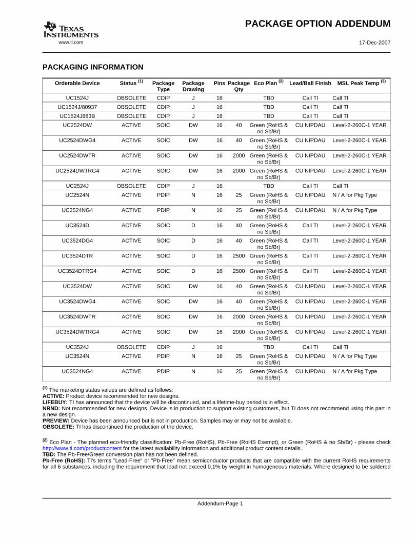
PACKAGING INFORMATION
Orderable Device Status (1) PackageType
PackageDrawing
Pins PackageQty
Eco Plan (2) Lead/Ball Finish MSL Peak Temp (3)
UC1524J OBSOLETE CDIP J 16 TBD Call TI Call TI
UC1524J/80937 OBSOLETE CDIP J 16 TBD Call TI Call TI
UC1524J883B OBSOLETE CDIP J 16 TBD Call TI Call TI
UC2524DW ACTIVE SOIC DW 16 40 Green (RoHS &no Sb/Br)
CU NIPDAU Level-2-260C-1 YEAR
UC2524DWG4 ACTIVE SOIC DW 16 40 Green (RoHS &no Sb/Br)
CU NIPDAU Level-2-260C-1 YEAR
UC2524DWTR ACTIVE SOIC DW 16 2000 Green (RoHS &no Sb/Br)
CU NIPDAU Level-2-260C-1 YEAR
UC2524DWTRG4 ACTIVE SOIC DW 16 2000 Green (RoHS &no Sb/Br)
CU NIPDAU Level-2-260C-1 YEAR
UC2524J OBSOLETE CDIP J 16 TBD Call TI Call TI
UC2524N ACTIVE PDIP N 16 25 Green (RoHS &no Sb/Br)
CU NIPDAU N / A for Pkg Type
UC2524NG4 ACTIVE PDIP N 16 25 Green (RoHS &no Sb/Br)
CU NIPDAU N / A for Pkg Type
UC3524D ACTIVE SOIC D 16 40 Green (RoHS &no Sb/Br)
Call TI Level-2-260C-1 YEAR
UC3524DG4 ACTIVE SOIC D 16 40 Green (RoHS &no Sb/Br)
Call TI Level-2-260C-1 YEAR
UC3524DTR ACTIVE SOIC D 16 2500 Green (RoHS &no Sb/Br)
Call TI Level-2-260C-1 YEAR
UC3524DTRG4 ACTIVE SOIC D 16 2500 Green (RoHS &no Sb/Br)
Call TI Level-2-260C-1 YEAR
UC3524DW ACTIVE SOIC DW 16 40 Green (RoHS &no Sb/Br)
CU NIPDAU Level-2-260C-1 YEAR
UC3524DWG4 ACTIVE SOIC DW 16 40 Green (RoHS &no Sb/Br)
CU NIPDAU Level-2-260C-1 YEAR
UC3524DWTR ACTIVE SOIC DW 16 2000 Green (RoHS &no Sb/Br)
CU NIPDAU Level-2-260C-1 YEAR
UC3524DWTRG4 ACTIVE SOIC DW 16 2000 Green (RoHS &no Sb/Br)
CU NIPDAU Level-2-260C-1 YEAR
UC3524J OBSOLETE CDIP J 16 TBD Call TI Call TI
UC3524N ACTIVE PDIP N 16 25 Green (RoHS &no Sb/Br)
CU NIPDAU N / A for Pkg Type
UC3524NG4 ACTIVE PDIP N 16 25 Green (RoHS &no Sb/Br)
CU NIPDAU N / A for Pkg Type
(1) The marketing status values are defined as follows:ACTIVE: Product device recommended for new designs.LIFEBUY: TI has announced that the device will be discontinued, and a lifetime-buy period is in effect.NRND: Not recommended for new designs. Device is in production to support existing customers, but TI does not recommend using this part ina new design.PREVIEW: Device has been announced but is not in production. Samples may or may not be available.OBSOLETE: TI has discontinued the production of the device.
(2) Eco Plan - The planned eco-friendly classification: Pb-Free (RoHS), Pb-Free (RoHS Exempt), or Green (RoHS & no Sb/Br) - please checkhttp://www.ti.com/productcontent for the latest availability information and additional product content details.TBD: The Pb-Free/Green conversion plan has not been defined.Pb-Free (RoHS): TI's terms "Lead-Free" or "Pb-Free" mean semiconductor products that are compatible with the current RoHS requirementsfor all 6 substances, including the requirement that lead not exceed 0.1% by weight in homogeneous materials. Where designed to be soldered
PACKAGE OPTION ADDENDUM
www.ti.com 17-Dec-2007
Addendum-Page 1
at high temperatures, TI Pb-Free products are suitable for use in specified lead-free processes.Pb-Free (RoHS Exempt): This component has a RoHS exemption for either 1) lead-based flip-chip solder bumps used between the die andpackage, or 2) lead-based die adhesive used between the die and leadframe. The component is otherwise considered Pb-Free (RoHScompatible) as defined above.Green (RoHS & no Sb/Br): TI defines "Green" to mean Pb-Free (RoHS compatible), and free of Bromine (Br) and Antimony (Sb) based flameretardants (Br or Sb do not exceed 0.1% by weight in homogeneous material)
(3) MSL, Peak Temp. -- The Moisture Sensitivity Level rating according to the JEDEC industry standard classifications, and peak soldertemperature.
Important Information and Disclaimer:The information provided on this page represents TI's knowledge and belief as of the date that it isprovided. TI bases its knowledge and belief on information provided by third parties, and makes no representation or warranty as to theaccuracy of such information. Efforts are underway to better integrate information from third parties. TI has taken and continues to takereasonable steps to provide representative and accurate information but may not have conducted destructive testing or chemical analysis onincoming materials and chemicals. TI and TI suppliers consider certain information to be proprietary, and thus CAS numbers and other limitedinformation may not be available for release.
In no event shall TI's liability arising out of such information exceed the total purchase price of the TI part(s) at issue in this document sold by TIto Customer on an annual basis.
PACKAGE OPTION ADDENDUM
www.ti.com 17-Dec-2007
Addendum-Page 2
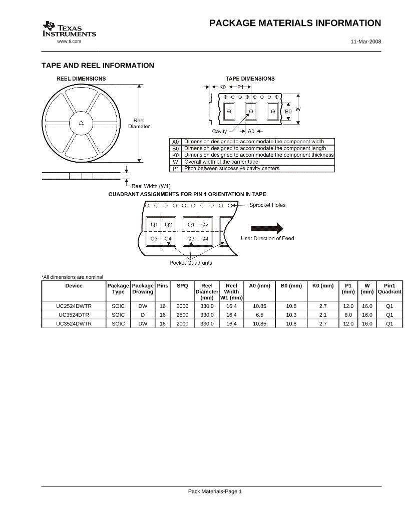
TAPE AND REEL INFORMATION
*All dimensions are nominal
Device PackageType
PackageDrawing
Pins SPQ ReelDiameter
(mm)
ReelWidth
W1 (mm)
A0 (mm) B0 (mm) K0 (mm) P1(mm)
W(mm)
Pin1Quadrant
UC2524DWTR SOIC DW 16 2000 330.0 16.4 10.85 10.8 2.7 12.0 16.0 Q1
UC3524DTR SOIC D 16 2500 330.0 16.4 6.5 10.3 2.1 8.0 16.0 Q1
UC3524DWTR SOIC DW 16 2000 330.0 16.4 10.85 10.8 2.7 12.0 16.0 Q1
PACKAGE MATERIALS INFORMATION
www.ti.com 11-Mar-2008
Pack Materials-Page 1
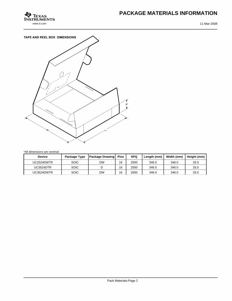
*All dimensions are nominal
Device Package Type Package Drawing Pins SPQ Length (mm) Width (mm) Height (mm)
UC2524DWTR SOIC DW 16 2000 346.0 346.0 33.0
UC3524DTR SOIC D 16 2500 346.0 346.0 33.0
UC3524DWTR SOIC DW 16 2000 346.0 346.0 33.0
PACKAGE MATERIALS INFORMATION
www.ti.com 11-Mar-2008
Pack Materials-Page 2
IMPORTANT NOTICETexas Instruments Incorporated and its subsidiaries (TI) reserve the right to make corrections, modifications, enhancements, improvements,and other changes to its products and services at any time and to discontinue any product or service without notice. Customers shouldobtain the latest relevant information before placing orders and should verify that such information is current and complete. All products aresold subject to TI’s terms and conditions of sale supplied at the time of order acknowledgment.TI warrants performance of its hardware products to the specifications applicable at the time of sale in accordance with TI’s standardwarranty. Testing and other quality control techniques are used to the extent TI deems necessary to support this warranty. Except wheremandated by government requirements, testing of all parameters of each product is not necessarily performed.TI assumes no liability for applications assistance or customer product design. Customers are responsible for their products andapplications using TI components. To minimize the risks associated with customer products and applications, customers should provideadequate design and operating safeguards.TI does not warrant or represent that any license, either express or implied, is granted under any TI patent right, copyright, mask work right,or other TI intellectual property right relating to any combination, machine, or process in which TI products or services are used. Informationpublished by TI regarding third-party products or services does not constitute a license from TI to use such products or services or awarranty or endorsement thereof. Use of such information may require a license from a third party under the patents or other intellectualproperty of the third party, or a license from TI under the patents or other intellectual property of TI.Reproduction of TI information in TI data books or data sheets is permissible only if reproduction is without alteration and is accompaniedby all associated warranties, conditions, limitations, and notices. Reproduction of this information with alteration is an unfair and deceptivebusiness practice. TI is not responsible or liable for such altered documentation. Information of third parties may be subject to additionalrestrictions.Resale of TI products or services with statements different from or beyond the parameters stated by TI for that product or service voids allexpress and any implied warranties for the associated TI product or service and is an unfair and deceptive business practice. TI is notresponsible or liable for any such statements.TI products are not authorized for use in safety-critical applications (such as life support) where a failure of the TI product would reasonablybe expected to cause severe personal injury or death, unless officers of the parties have executed an agreement specifically governingsuch use. Buyers represent that they have all necessary expertise in the safety and regulatory ramifications of their applications, andacknowledge and agree that they are solely responsible for all legal, regulatory and safety-related requirements concerning their productsand any use of TI products in such safety-critical applications, notwithstanding any applications-related information or support that may beprovided by TI. Further, Buyers must fully indemnify TI and its representatives against any damages arising out of the use of TI products insuch safety-critical applications.TI products are neither designed nor intended for use in military/aerospace applications or environments unless the TI products arespecifically designated by TI as military-grade or "enhanced plastic." Only products designated by TI as military-grade meet militaryspecifications. Buyers acknowledge and agree that any such use of TI products which TI has not designated as military-grade is solely atthe Buyer's risk, and that they are solely responsible for compliance with all legal and regulatory requirements in connection with such use.TI products are neither designed nor intended for use in automotive applications or environments unless the specific TI products aredesignated by TI as compliant with ISO/TS 16949 requirements. Buyers acknowledge and agree that, if they use any non-designatedproducts in automotive applications, TI will not be responsible for any failure to meet such requirements.Following are URLs where you can obtain information on other Texas Instruments products and application solutions:Products ApplicationsAmplifiers amplifier.ti.com Audio www.ti.com/audioData Converters dataconverter.ti.com Automotive www.ti.com/automotiveDSP dsp.ti.com Broadband www.ti.com/broadbandClocks and Timers www.ti.com/clocks Digital Control www.ti.com/digitalcontrolInterface interface.ti.com Medical www.ti.com/medicalLogic logic.ti.com Military www.ti.com/militaryPower Mgmt power.ti.com Optical Networking www.ti.com/opticalnetworkMicrocontrollers microcontroller.ti.com Security www.ti.com/securityRFID www.ti-rfid.com Telephony www.ti.com/telephonyRF/IF and ZigBee® Solutions www.ti.com/lprf Video & Imaging www.ti.com/video
Wireless www.ti.com/wireless
Mailing Address: Texas Instruments, Post Office Box 655303, Dallas, Texas 75265Copyright © 2008, Texas Instruments Incorporated