Embed Size (px)
Citation preview

Advanced Optical Inspection TechniquesSeptember 9, 2010
Andrei Brunfeld
2
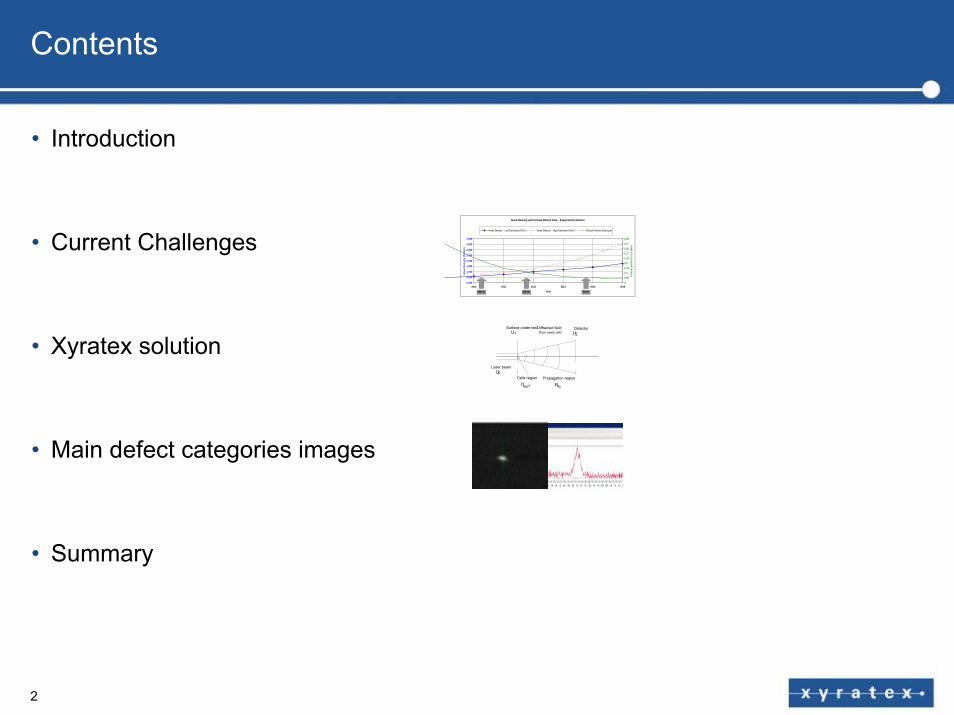
Contents
• Introduction
• Current Challenges
• Xyratex solution
• Main defect categories images
• Summary
Areal Density and Critical Defect Size - Expected Evolution
0.000
0.500
1.000
1.500
2.000
2.500
3.000
3.500
4.000
2010 2011 2012 2013 2014 2015
Year
Area
l Den
sity
(Tb/
in2)
0
0.05
0.1
0.15
0.2
0.25
0.3
0.35
0.4
0.45
Criti
cal p
artic
le s
ize
(um
)
Areal Density - Low Estimate (Tb/in²) Areal Density - High Estimate (Tb/in²) Critical Particle Size (µm)
200nm 100nm 50nm
Laser beam
Detector Surface under test
Cells region
Diffracted field(from every cell)
U0Propagation region
U 1U 2
Πsurf R 2z
In-Line Testing Challenges
Brief Review
4
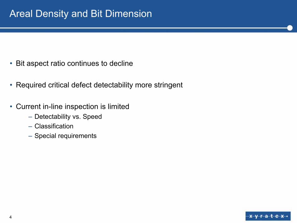
Areal Density and Bit Dimension
• Bit aspect ratio continues to decline
• Required critical defect detectability more stringent
• Current in-line inspection is limited– Detectability vs. Speed– Classification– Special requirements
5
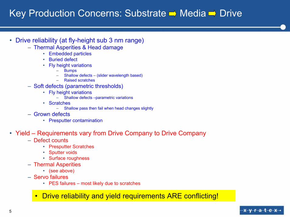
Key Production Concerns: Substrate Media Drive
• Drive reliability (at fly-height sub 3 nm range)– Thermal Asperities & Head damage
• Embedded particles• Buried defect• Fly height variations
– Bumps– Shallow defects – (slider wavelength based)– Raised scratches
– Soft defects (parametric thresholds)• Fly height variations
– Shallow defects –parametric variations• Scratches
– Shallow pass then fail when head changes slightly– Grown defects
• Presputter contamination
• Yield – Requirements vary from Drive Company to Drive Company– Defect counts
• Presputter Scratches• Sputter voids• Surface roughness
– Thermal Asperities• (see above)
– Servo failures• PES failures – most likely due to scratches
• Drive reliability and yield requirements ARE conflicting!
6
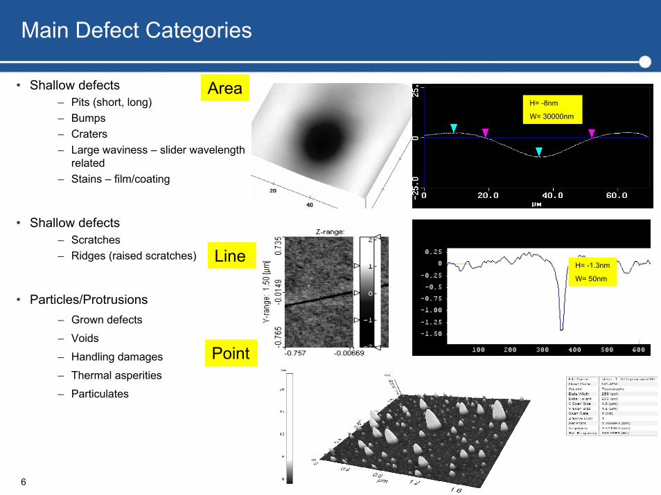
Main Defect Categories
• Shallow defects– Pits (short, long)– Bumps – Craters– Large waviness – slider wavelength
related– Stains – film/coating
• Shallow defects– Scratches– Ridges (raised scratches)
• Particles/Protrusions– Grown defects
– Voids
– Handling damages
– Thermal asperities
– Particulates
AreaH= -8nm
W= 30000nm
H= -1.3nm
W= 50nm
Line
Point
7
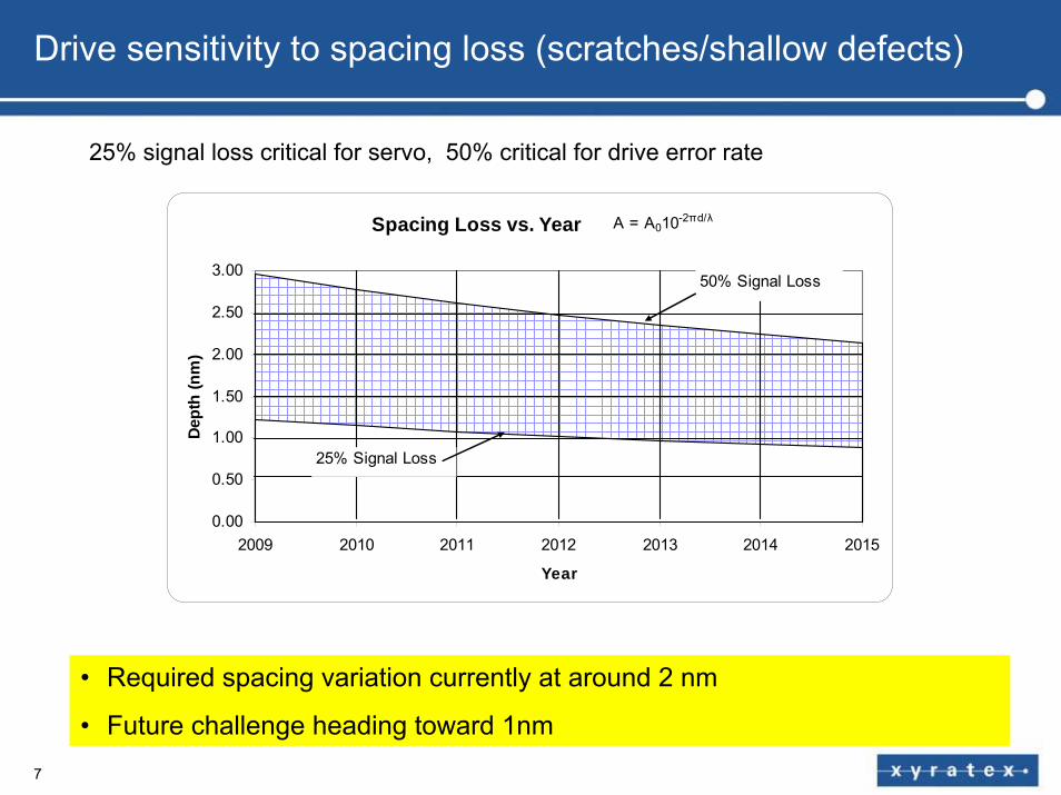
Drive sensitivity to spacing loss (scratches/shallow defects)
25% signal loss critical for servo, 50% critical for drive error rate
Spacing Loss vs. Year
0.00
0.50
1.00
1.50
2.00
2.50
3.00
2009 2010 2011 2012 2013 2014 2015
Year
Dept
h (n
m)
A = A010-2πd/λ
25% Signal Loss
50% Signal Loss
• Required spacing variation currently at around 2 nm
• Future challenge heading toward 1nm
8
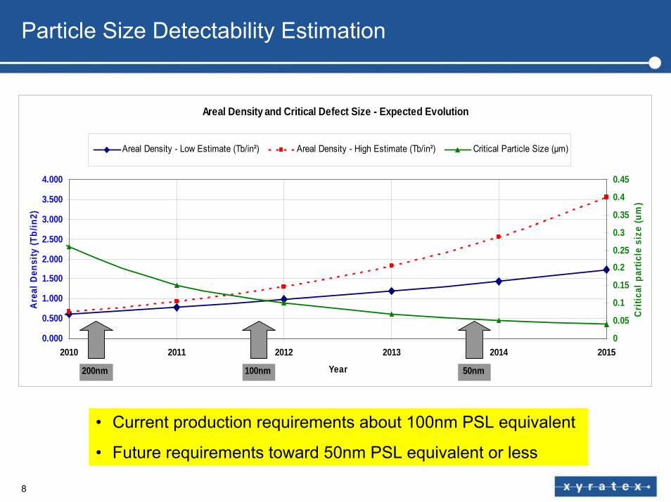
Particle Size Detectability Estimation
Areal Density and Critical Defect Size - Expected Evolution
0.000
0.500
1.000
1.500
2.000
2.500
3.000
3.500
4.000
2010 2011 2012 2013 2014 2015
Year
Area
l Den
sity
(Tb/
in2)
0
0.05
0.1
0.15
0.2
0.25
0.3
0.35
0.4
0.45
Cri
tical
par
ticle
siz
e (u
m)
Areal Density - Low Estimate (Tb/in²) Areal Density - High Estimate (Tb/in²) Critical Particle Size (µm)
200nm 100nm 50nm
• Current production requirements about 100nm PSL equivalent
• Future requirements toward 50nm PSL equivalent or less
9
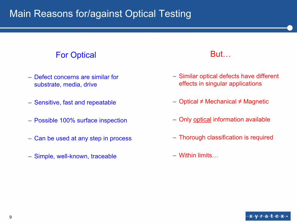
Main Reasons for/against Optical Testing
But…
– Similar optical defects have different effects in singular applications
– Optical ≠ Mechanical ≠ Magnetic
– Only optical information available
– Thorough classification is required
– Within limits…
For Optical
– Defect concerns are similar for substrate, media, drive
– Sensitive, fast and repeatable
– Possible 100% surface inspection
– Can be used at any step in process
– Simple, well-known, traceable
10
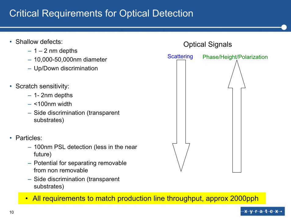
Critical Requirements for Optical Detection
• Shallow defects:– 1 – 2 nm depths– 10,000-50,000nm diameter – Up/Down discrimination
• Scratch sensitivity:– 1- 2nm depths – <100nm width– Side discrimination (transparent
substrates)
• Particles:– 100nm PSL detection (less in the near
future)– Potential for separating removable
from non removable– Side discrimination (transparent
substrates)
Optical SignalsScattering Phase/Height/Polarization
• All requirements to match production line throughput, approx 2000pph
11
Current optical inspection systems concepts
• Monolithic: Single inspection head, single spindle– High sensitivity– Multiple signal channels: dark-field, bright-field, polarization, etc.– Small spot size– High classification level– Limited speed
• Monolithic: Single inspection head, multiple spindles– High speed – Dark-field and bright-field– Large spot size– Limited classification
• Modular: Multiple inspection heads, multiple spindles– Miniature optical head– High sensitivity and high speed– Dark-field and bright-field– Medium spot size– High classification versatility– Distributed test recipes available for each head+spindle system– Special tests (e.g. for glass: side discrimination, cracked disk)
Xyratex Sensor
13
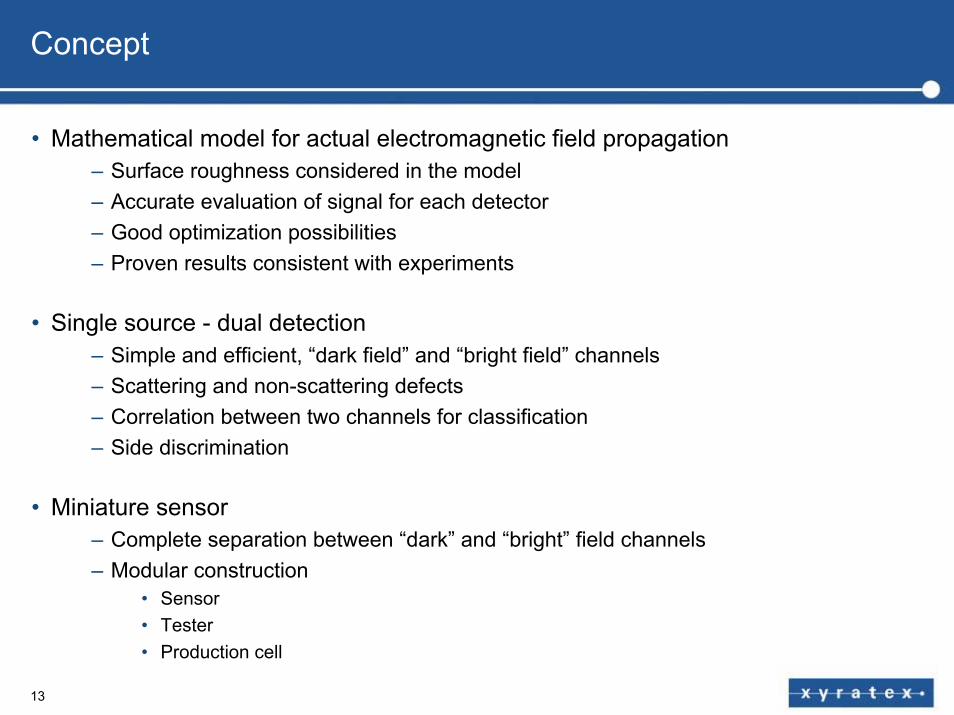
Concept
• Mathematical model for actual electromagnetic field propagation– Surface roughness considered in the model– Accurate evaluation of signal for each detector– Good optimization possibilities– Proven results consistent with experiments
• Single source - dual detection– Simple and efficient, “dark field” and “bright field” channels– Scattering and non-scattering defects– Correlation between two channels for classification– Side discrimination
• Miniature sensor– Complete separation between “dark” and “bright” field channels– Modular construction
• Sensor• Tester• Production cell
14
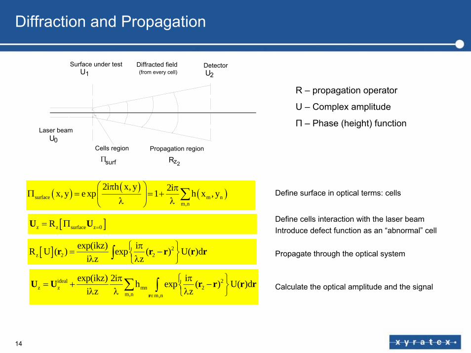
Diffraction and Propagation
Laser beam
Detector Surface under test
Cells region
Diffracted field(from every cell)
U0Propagation region
U 1U 2
Πsurf R 2z
R – propagation operator
U – Complex amplitude
Π – Phase (height) function
Define surface in optical terms: cells
Define cells interaction with the laser beamIntroduce defect function as an “abnormal” cell
Propagate through the optical system
Calculate the optical amplitude and the signal
[ ]z z surface z 0R == ΠU U
( ) ( ) ( )surface m nm,n
2i h x, y 2ix, y e xp 1 h x , y⎛ ⎞π π
Π = = +⎜ ⎟λ λ⎝ ⎠∑
[ ] 2z 2 2
exp(ikz) iR U ( ) exp ( ) U( )di z z
π⎧ ⎫= −⎨ ⎬λ λ⎩ ⎭∫r r r r r
ideal 2z z mn 2
m,n m,n
exp(ikz) 2i ih exp ( ) U( )di z z∈
π π⎧ ⎫= + −⎨ ⎬λ λ λ⎩ ⎭
∑ ∫r
U U r r r r
15
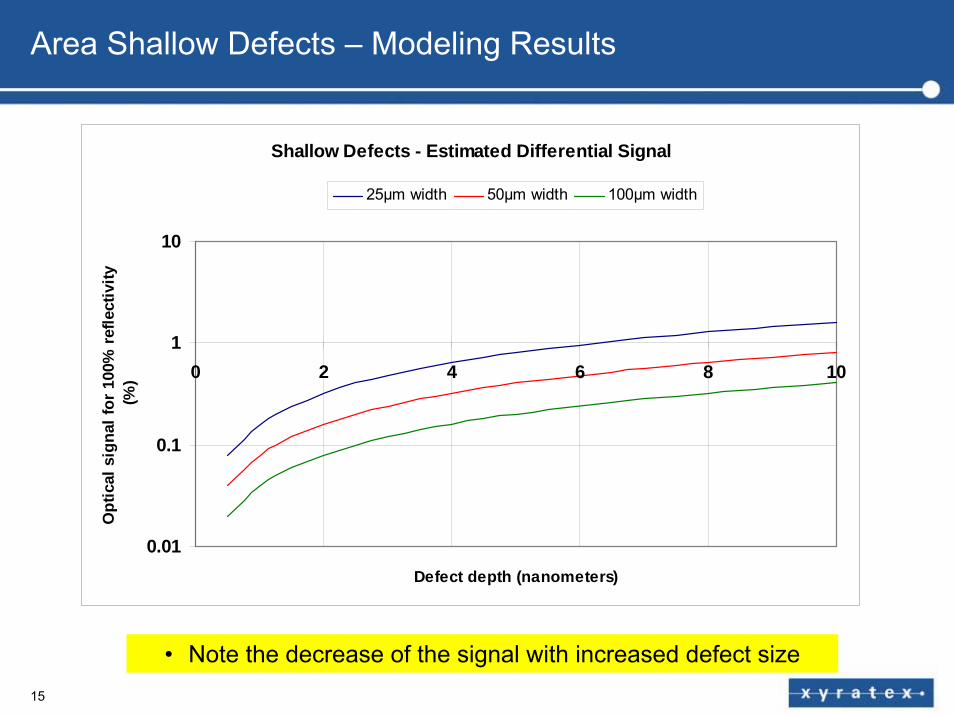
Area Shallow Defects – Modeling Results
Shallow Defects - Estimated Differential Signal
0.01
0.1
1
10
0 2 4 6 8 10
Defect depth (nanometers)
Opt
ical
sig
nal f
or 1
00%
ref
lect
ivity
(%
)
25µm width 50µm width 100µm width
• Note the decrease of the signal with increased defect size
16
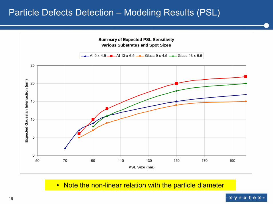
Particle Defects Detection – Modeling Results (PSL)
Summary of Expected PSL SensitivityVarious Substrates and Spot Sizes
0
5
10
15
20
25
50 70 90 110 130 150 170 190
PSL Size (nm)
Exp
ecte
d G
auss
ian
Inte
rrac
tion
(um
)
Al 9 x 4.5 Al 13 x 6.5 Glass 9 x 4.5 Glass 13 x 6.5
• Note the non-linear relation with the particle diameter
Main Defect Categories - Images
18
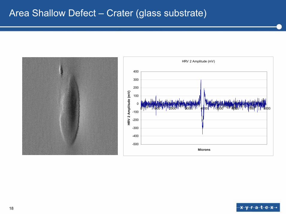
Area Shallow Defect – Crater (glass substrate)
HRV 2 Amplitude (mV)
-500
-400
-300
-200
-100
0
100
200
300
400
0 1000 2000 3000 4000 5000 6000 7000 8000
Microns
HRV
2 A
mpl
itude
(mV
)
19
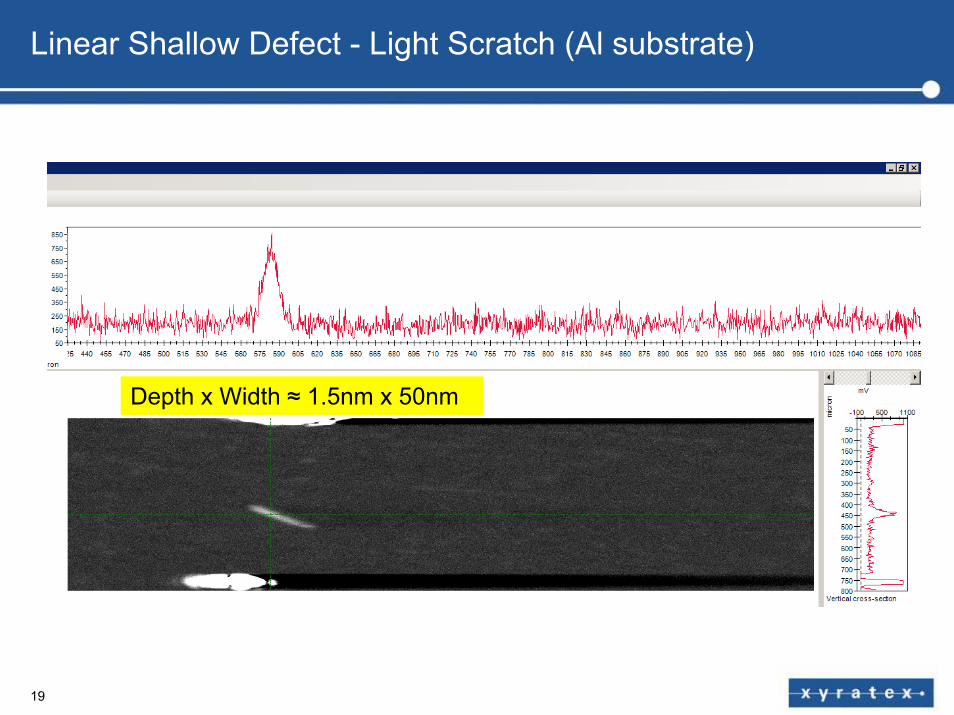
Linear Shallow Defect - Light Scratch (Al substrate)
Depth x Width ≈ 1.5nm x 50nm
20
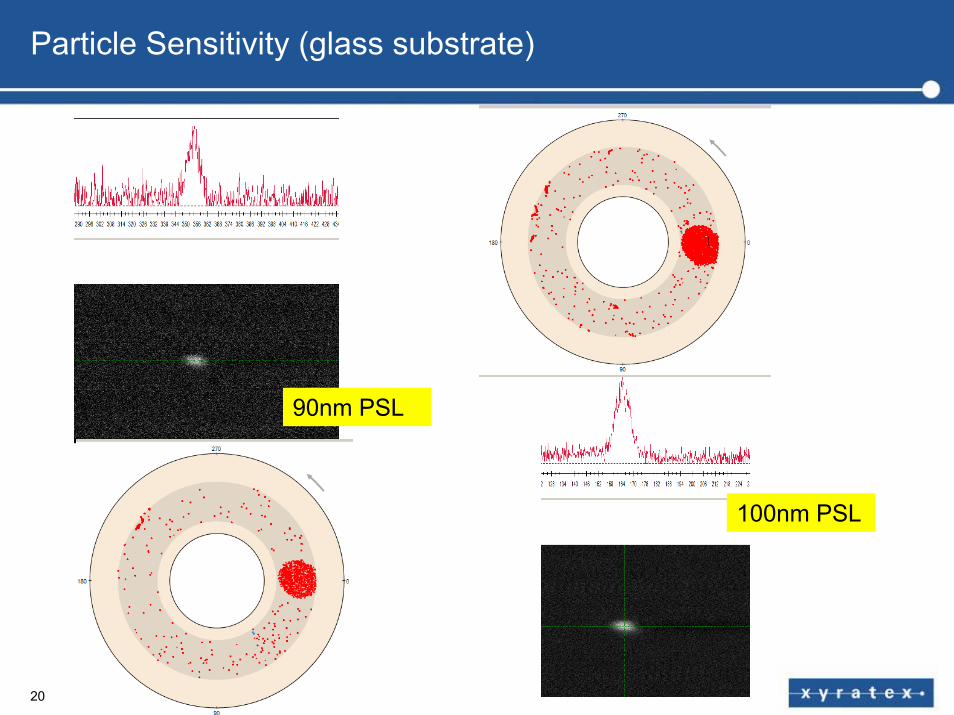
Particle Sensitivity (glass substrate)
90nm PSL
100nm PSL
21
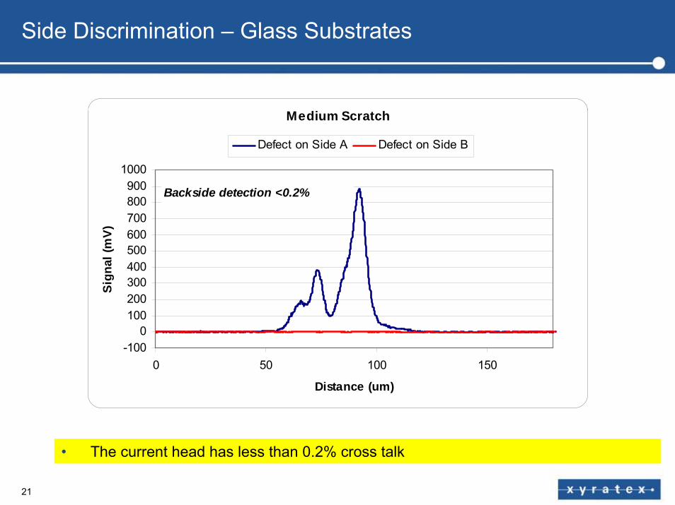
Side Discrimination – Glass Substrates
Medium Scratch
-1000
100200300400500600700800900
1000
0 50 100 150
Distance (um)
Sign
al (m
V)
Defect on Side A Defect on Side B
Backside detection <0.2%
• The current head has less than 0.2% cross talk
22
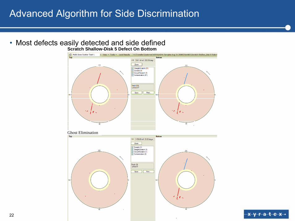
Advanced Algorithm for Side Discrimination
• Most defects easily detected and side definedScratch Shallow-Disk 5 Defect On Bottom
Ghost Elimination
23
Summary
• Focus on optical testing– Bit density vs. defect size– Production concerns– Optical testing – pro and contra– Detection requirements/challenges– Throughput
• Xyratex sensor– Concept– Modularity– Maps of main detector categories
• Contributors– Andrei Brunfeld– Bryan Clark– Gregory Toker– Morey Roscrow– Peter Goglia
• Entire Titan project team