Embed Size (px)
Citation preview
Advanced Concepts, Part 1
Lecture 15 – 11/3/2011 MIT Fundamentals of Photovoltaics
2.626/2.627 Joseph T. Sullivan
1

Cells are done!
2
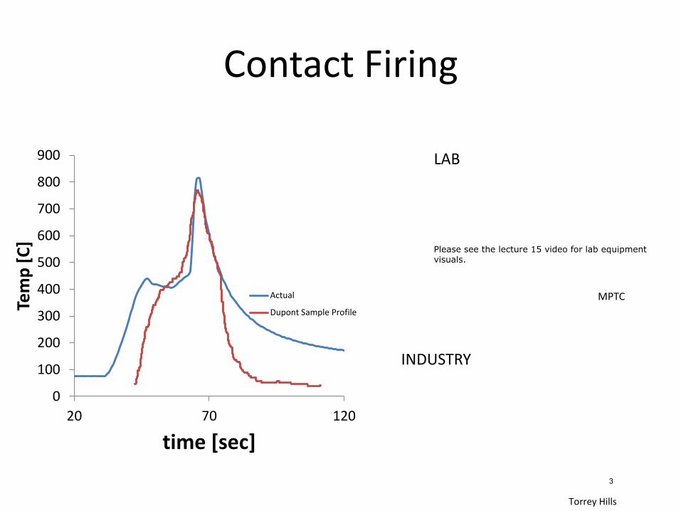
Contact Firing
0
100
200
300
400
500
600
700
800
900
20 70 120
Tem
p [
C]
time [sec]
Actual
Dupont Sample Profile
LAB
INDUSTRY
Torrey Hills
MPTC
Please see the lecture 15 video for lab equipmentvisuals.
3
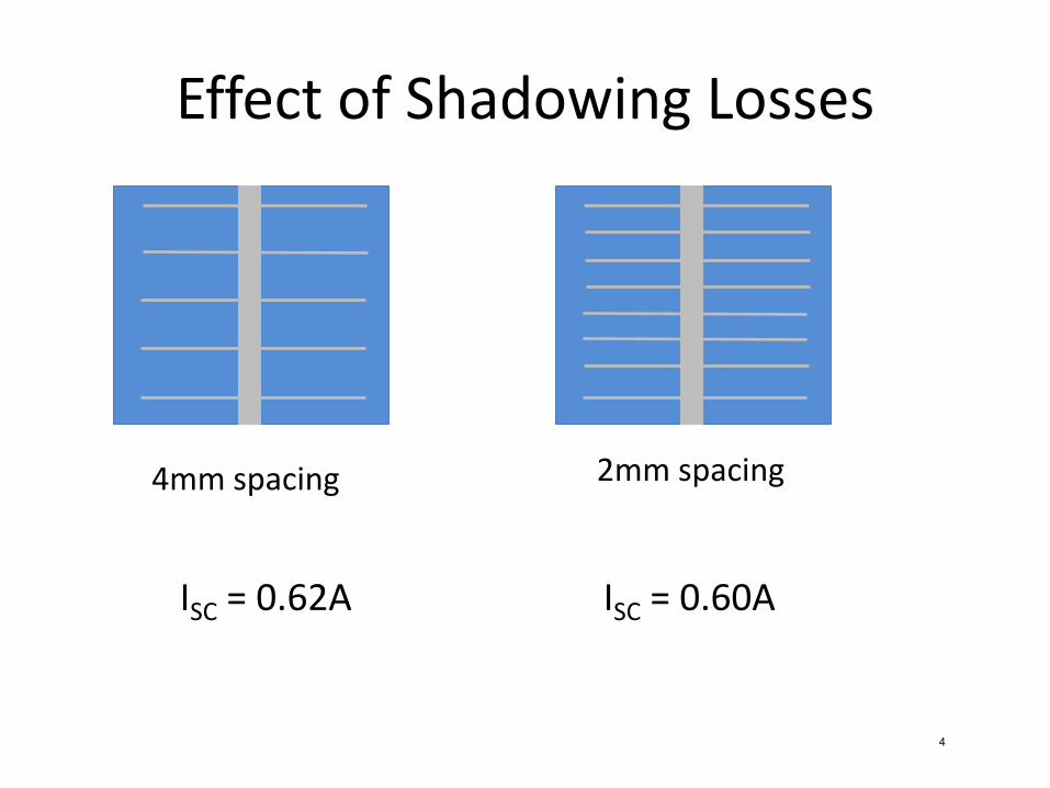
Effect of Shadowing Losses
4mm spacing 2mm spacing
ISC = 0.62A ISC = 0.60A
4

What’s Limiting Performance?
0.1
0.11
0.12
0.13
0.14
0.15
0.16
0.17
0.18
0.19
0.2
0 0.2 0.4 0.6 0.8 1 1.2
PM
ax [
W]
Series Resistance [Ohms]
Rs
What are the different forms of series resistance?
5
Performance in the Field: Temperature, Shading, and
Mismatch
6

Why Temperature Matters
• Solar cell efficiency measurements are performed at 25°C
• Most Semiconductor simulations occur at 300K (27°C)
• Typical Solar Cell operate at 50-65°C
7
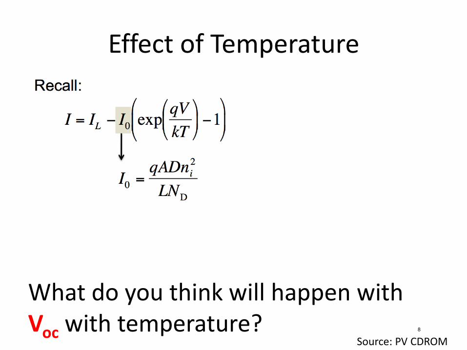
Effect of Temperature
What do you think will happen with Voc with temperature?
Source: PV CDROM 8
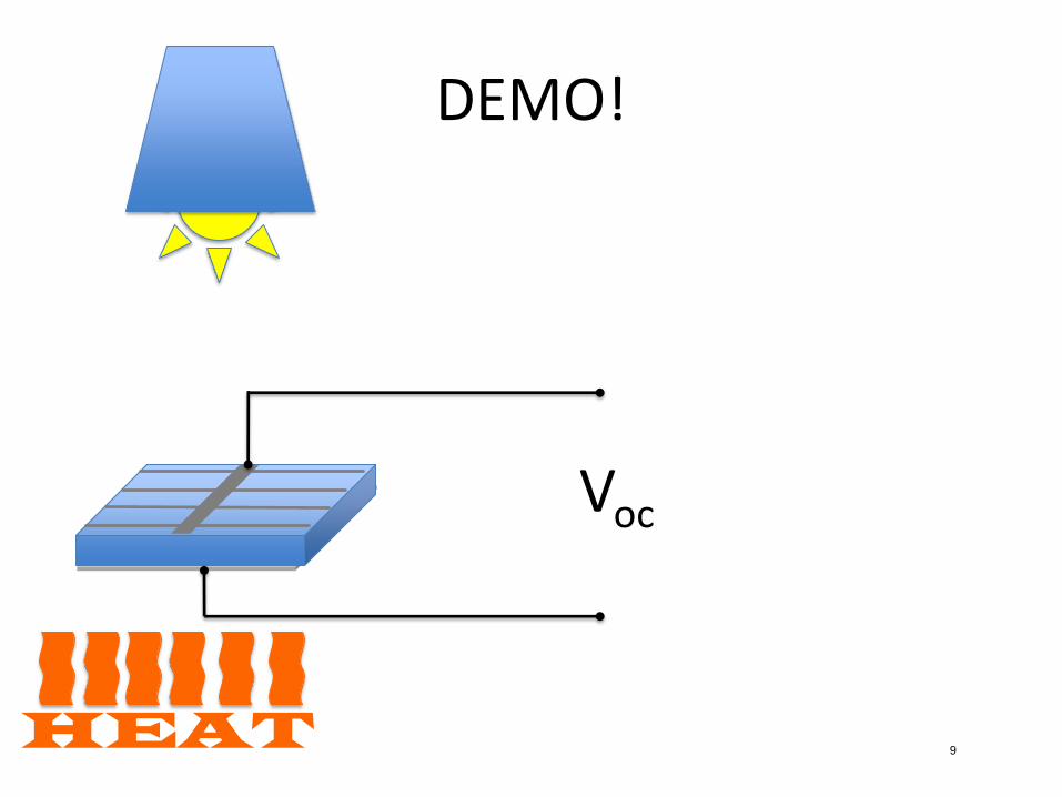
DEMO!
Voc
HEAT 9
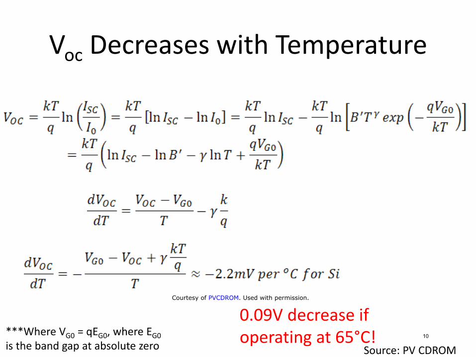
Voc Decreases with Temperature
***Where VG0 = qEG0, where EG0 is the band gap at absolute zero Source: PV CDROM
0.09V decrease if operating at 65°C!
Courtesy of PVCDROM. Used with permission.
10
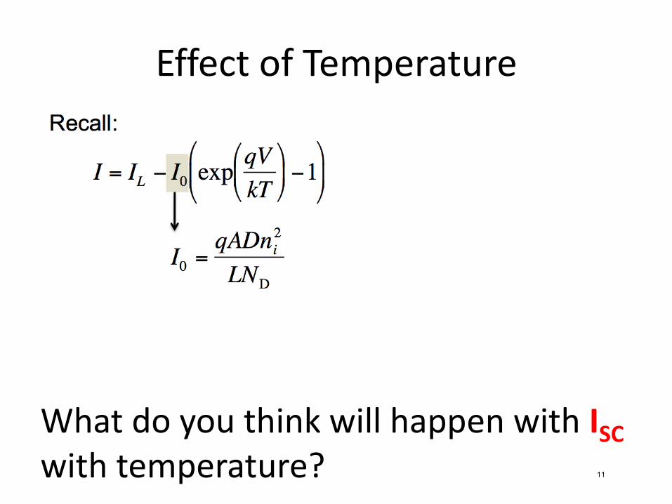
Effect of Temperature
What do you think will happen with ISC with temperature? 11

DEMO 2!
ISC
HEAT
A
12
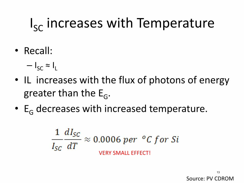
ISC increases with Temperature
• Recall:
– ISC ≈ IL
• IL increases with the flux of photons of energy greater than the EG.
• EG decreases with increased temperature.
Source: PV CDROM
VERY SMALL EFFECT!
13
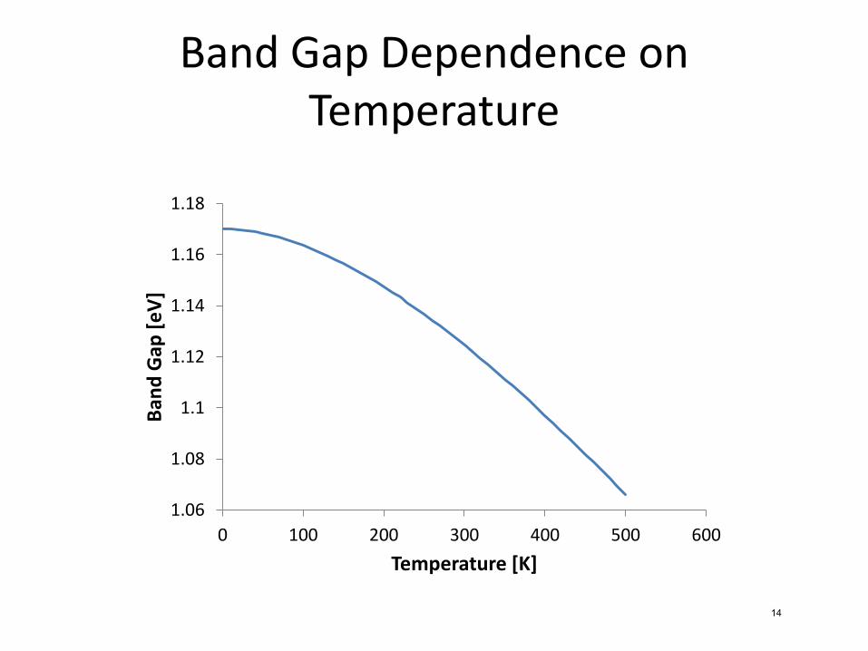
Band Gap Dependence on Temperature
1.06
1.08
1.1
1.12
1.14
1.16
1.18
0 100 200 300 400 500 600
Ban
d G
ap [
eV
]
Temperature [K]
14
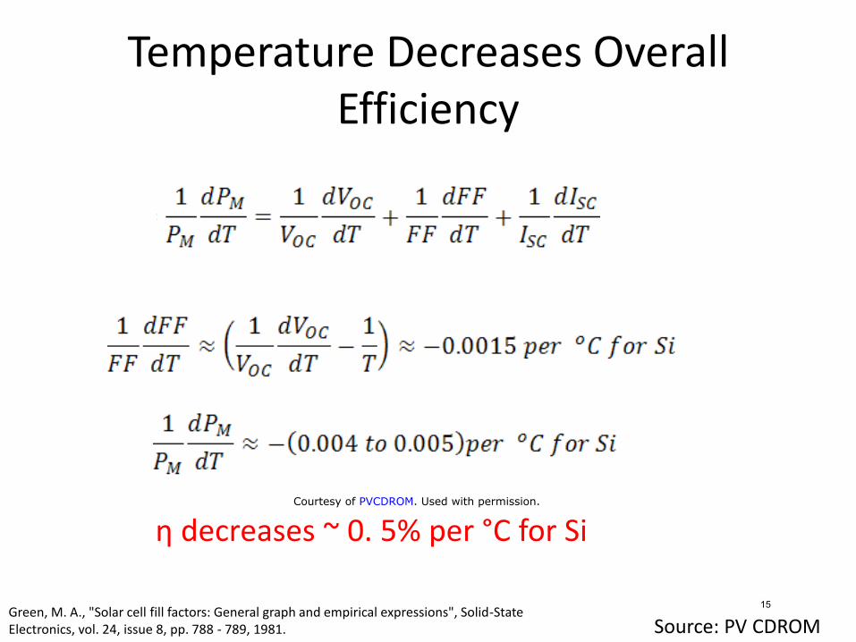
Temperature Decreases Overall Efficiency
Green, M. A., "Solar cell fill factors: General graph and empirical expressions", Solid-State Electronics, vol. 24, issue 8, pp. 788 - 789, 1981. Source: PV CDROM
η decreases ~ 0. 5% per °C for Si
15
Courtesy of PVCDROM. Used with permission.
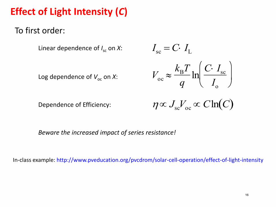
Effect of Light Intensity (C)
To first order:
Isc C IL
Voc kBT
qlnC Isc
Io
JscVoc C ln C
Linear dependence of Isc on X:
Log dependence of Voc on X:
Dependence of Efficiency:
In-class example: http://www.pveducation.org/pvcdrom/solar-cell-operation/effect-of-light-intensity
Beware the increased impact of series resistance!
16
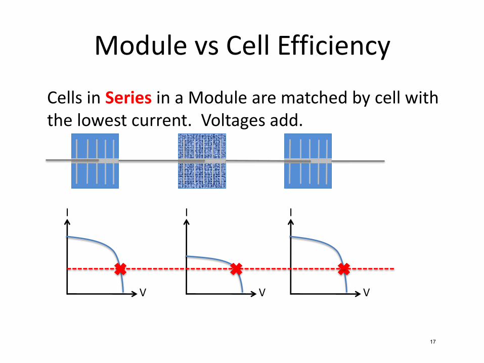
Module vs Cell Efficiency
Cells in Series in a Module are matched by cell with the lowest current. Voltages add.
I
V
I
V
I
V
17
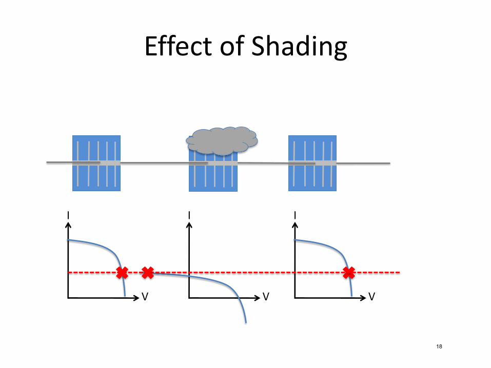
Effect of Shading
I
V
I
V
I
V
18
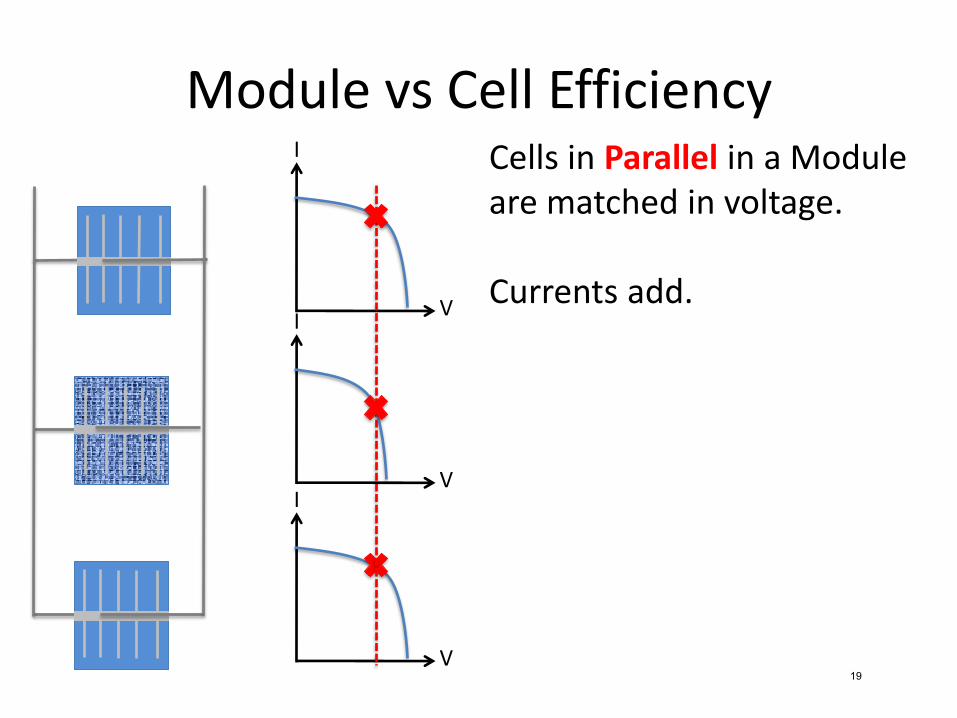
Module vs Cell Efficiency Cells in Parallel in a Module are matched in voltage. Currents add.
I
V
I
V
I
V
19

Effect of Inhomogeneities
Source: PV CDROM 20
Courtesy of PVCDROM. Used with permission.
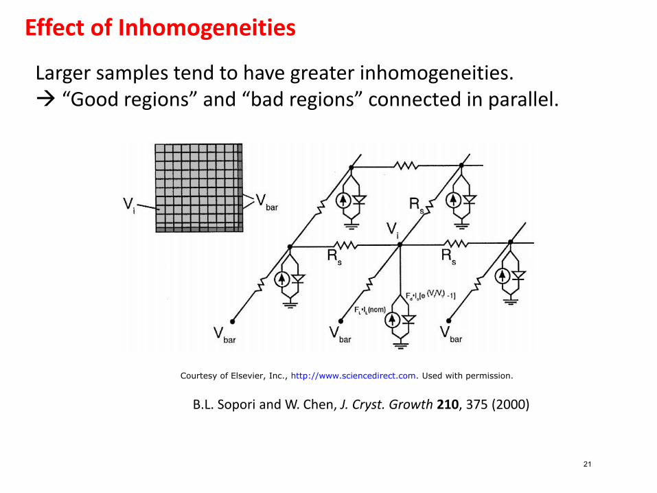
Effect of Inhomogeneities
B.L. Sopori and W. Chen, J. Cryst. Growth 210, 375 (2000)
Larger samples tend to have greater inhomogeneities. “Good regions” and “bad regions” connected in parallel.
Courtesy of Elsevier, Inc., http://www.sciencedirect.com. Used with permission.
21
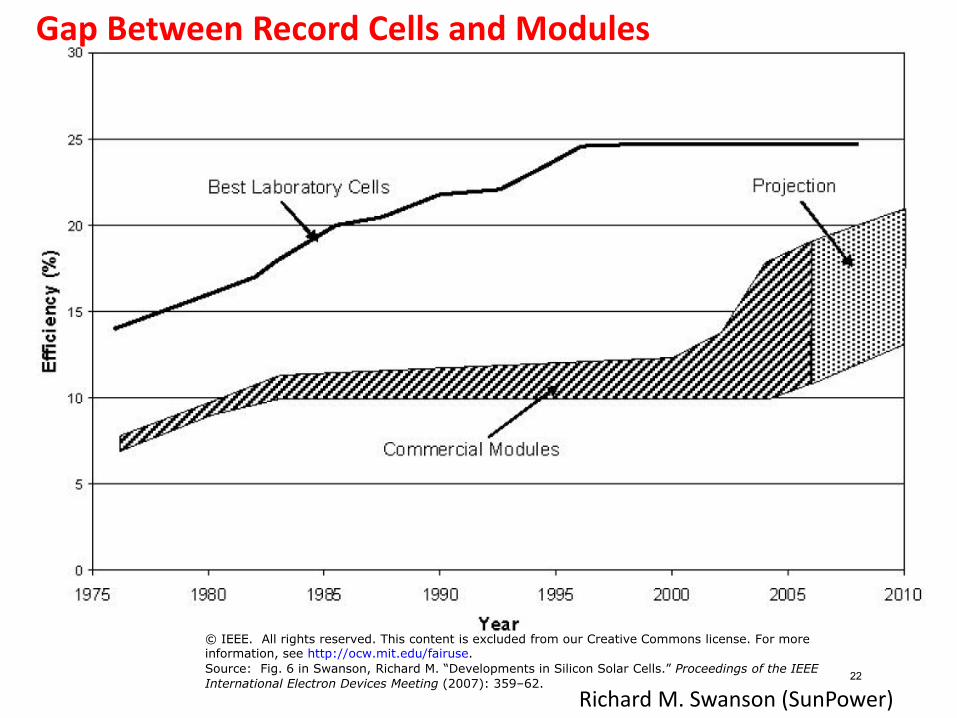
Richard M. Swanson (SunPower)
Gap Between Record Cells and Modules
© IEEE. All rights reserved. This content is excluded from our Creative Commons license. For moreinformation, see http://ocw.mit.edu/fairuse.
Source: Fig. 6 in Swanson, Richard M. “Developments in Silicon Solar Cells.” Proceedings of the IEEEInternational Electron Devices Meeting (2007): 359–62.
22

Advanced Concepts
23
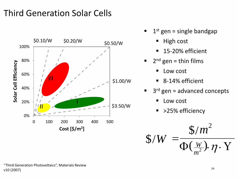
1st gen = single bandgap
High cost
15-20% efficient
2nd gen = thin films
Low cost
8-14% efficient
3rd gen = advanced concepts
Low cost
>25% efficiency
Third Generation Solar Cells
“Third Generation Photovoltaics”, Materials Review v10 (2007)
0%
20%
40%
60%
80%
100%
0 100 200 300 400 500
Sola
r C
ell
Effi
cie
ncy
Cost [$/m2]
$3.50/W
$1.00/W
$0.50/W $0.20/W $0.10/W
I II
III
)(
2m// WW
$$
2m
24
Intermediate Band Materials
25

Absorption of Photons in a Semiconductor
Conduction Band
Valence Band
E
DOS
e-
e-
e-
Eg
E
26
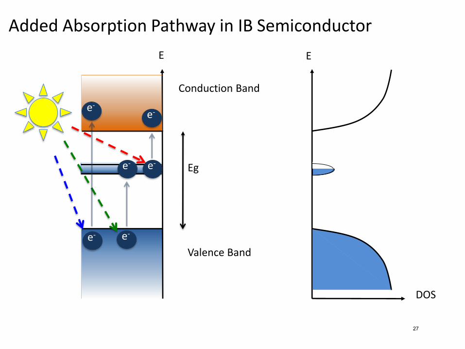
Added Absorption Pathway in IB Semiconductor
Conduction Band
Valence Band
Eg
E
DOS
e-
e-
e-
e-
e-
e-
E
27
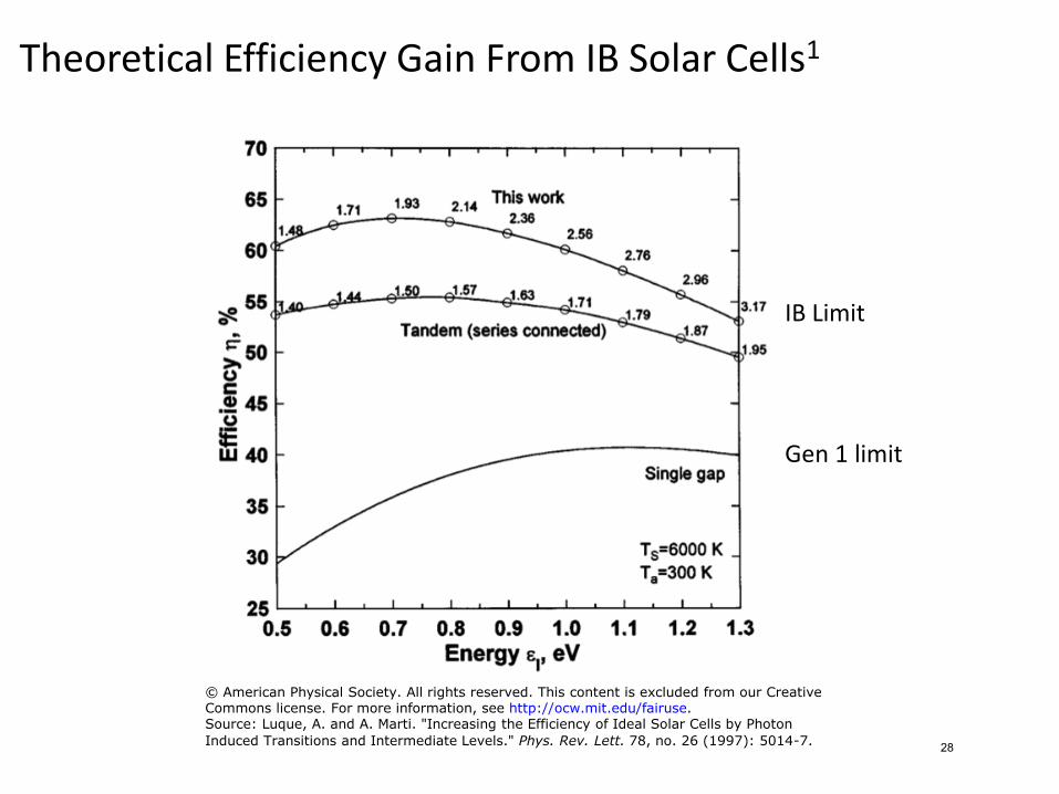
Theoretical Efficiency Gain From IB Solar Cells1
Gen 1 limit
IB Limit
© American Physical Society. All rights reserved. This content is excluded from our CreativeCommons license. For more information, see http://ocw.mit.edu/fairuse.Source: Luque, A. and A. Marti. "Increasing the Efficiency of Ideal Solar Cells by Photon
Induced Transitions and Intermediate Levels." Phys. Rev. Lett. 78, no. 26 (1997): 5014-7. 28
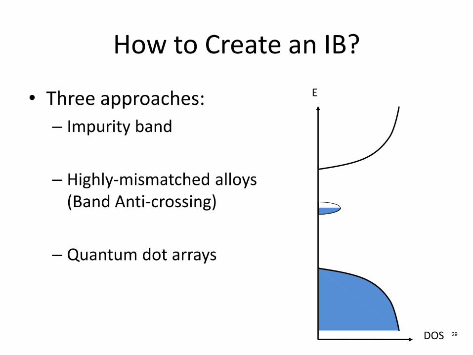
How to Create an IB?
• Three approaches:
– Impurity band
– Highly-mismatched alloys (Band Anti-crossing)
– Quantum dot arrays
E
DOS 29

Impurity Band
ND
< N
crit
aB
[1] A. Luque, A. Martí, E. Antolín, and C. Tablero, Physica B 382, 320 (2006)[2] A. Luque and A. Martí, Solid State Phenomena 156-158, 107 (2010)
30
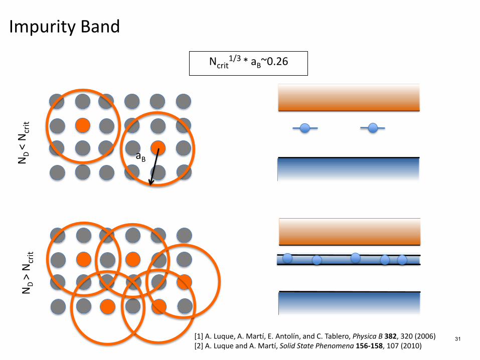
Impurity Band
Ncrit1/3 * aB~0.26
ND
> N
crit
N
D <
Ncr
it
aB
[1] A. Luque, A. Martí, E. Antolín, and C. Tablero, Physica B 382, 320 (2006)[2] A. Luque and A. Martí, Solid State Phenomena 156-158, 107 (2010)
31
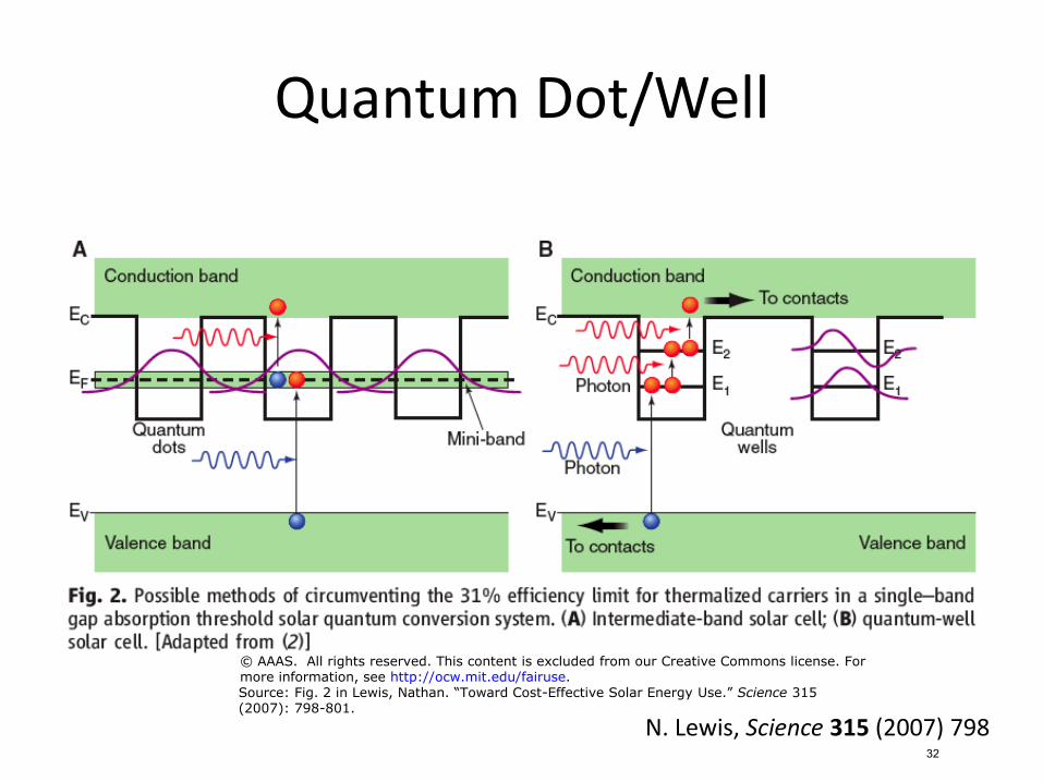
Quantum Dot/Well
N. Lewis, Science 315 (2007) 798
© AAAS. All rights reserved. This content is excluded from our Creative Commons license. Formore information, see http://ocw.mit.edu/fairuse.Source: Fig. 2 in Lewis, Nathan. “Toward Cost-Effective Solar Energy Use.” Science 315(2007): 798-801.
32

López et al. “Engineering the Electronic Band Structure for Multiband Solar Cells.” Phys. Rev. Lett. 106, no. 2 (2011): 028701.
Band-Anticrossing
Yu et al. “Diluted II-VI oxide semiconductors with multiple band gaps.” Phys. Rev. Lett. 91, no. 24 (2003): 246403.
Please see lecture 15 video or the references below for relevant band diagram visuals.
33
Hot Carrier Cells
34
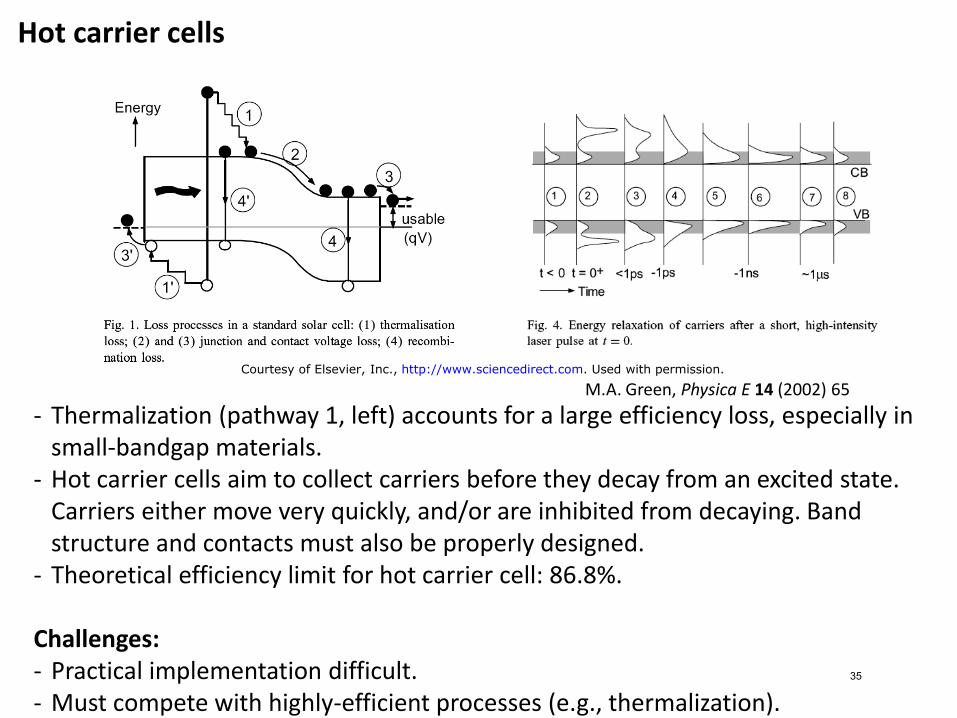
Hot carrier cells
- Thermalization (pathway 1, left) accounts for a large efficiency loss, especially in small-bandgap materials.
- Hot carrier cells aim to collect carriers before they decay from an excited state. Carriers either move very quickly, and/or are inhibited from decaying. Band structure and contacts must also be properly designed.
- Theoretical efficiency limit for hot carrier cell: 86.8%.
Challenges: - Practical implementation difficult. - Must compete with highly-efficient processes (e.g., thermalization).
M.A. Green, Physica E 14 (2002) 65 Courtesy of Elsevier, Inc., http://www.sciencedirect.com. Used with permission.
35
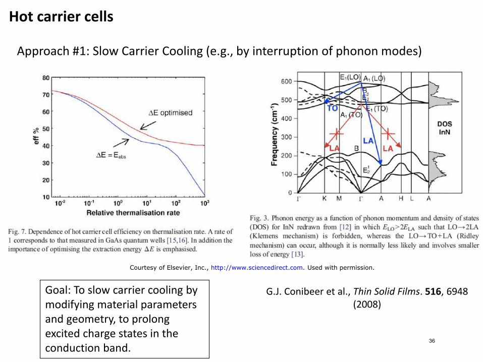
Hot carrier cells
Approach #1: Slow Carrier Cooling (e.g., by interruption of phonon modes)
G.J. Conibeer et al., Thin Solid Films. 516, 6948 (2008)
Goal: To slow carrier cooling by modifying material parameters and geometry, to prolong excited charge states in the conduction band.
Courtesy of Elsevier, Inc., http://www.sciencedirect.com. Used with permission.
36

Hot carrier cells
Approach #2: Selective Energy Contacts
G.J. Conibeer et al., Thin Solid Films 516 6968 (2008)
Goal: To extract hot carriers from devices, e.g., via resonant tunneling contacts.
Courtesy of Elsevier, Inc., http://www.sciencedirect.com. Used with permission.
37

Emerging Tech: Bulk Thin Films
38
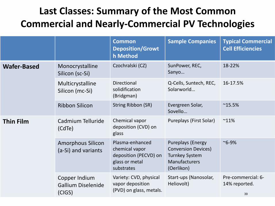
Last Classes: Summary of the Most Common Commercial and Nearly-Commercial PV Technologies
Common Deposition/Growth Method
Sample Companies Typical Commercial Cell Efficiencies
Wafer-Based Monocrystalline Silicon (sc-Si)
Czochralski (CZ) SunPower, REC, Sanyo…
18-22%
Multicrystalline Silicon (mc-Si)
Directional solidification (Bridgman)
Q-Cells, Suntech, REC, Solarworld…
16-17.5%
Ribbon Silicon String Ribbon (SR) Evergreen Solar, Sovello…
~15.5%
Thin Film Cadmium Telluride (CdTe)
Chemical vapor deposition (CVD) on glass
Pureplays (First Solar) ~11%
Amorphous Silicon (a-Si) and variants
Plasma-enhanced chemical vapor deposition (PECVD) on glass or metal substrates
Pureplays (Energy Conversion Devices) Turnkey System Manufacturers (Oerlikon)
~6-9%
Copper Indium Gallium Diselenide (CIGS)
Variety: CVD, physical vapor deposition (PVD) on glass, metals.
Start-ups (Nanosolar, Heliovolt)
Pre-commercial: 6-14% reported.
39
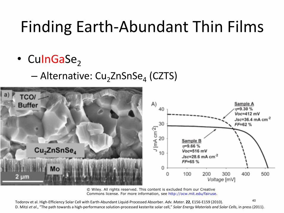
Finding Earth-Abundant Thin Films
• CuInGaSe2
– Alternative: Cu2ZnSnSe4 (CZTS)
Todorov et al. High‐Efficiency Solar Cell with Earth‐Abundant Liquid‐Processed Absorber. Adv. Mater. 22, E156-E159 (2010). D. Mitzi et al., “The path towards a high-performance solution-processed kesterite solar cell,” Solar Energy Materials and Solar Cells, in press (2011).
© Wiley. All rights reserved. This content is excluded from our CreativeCommons license. For more information, see http://ocw.mit.edu/fairuse.
40
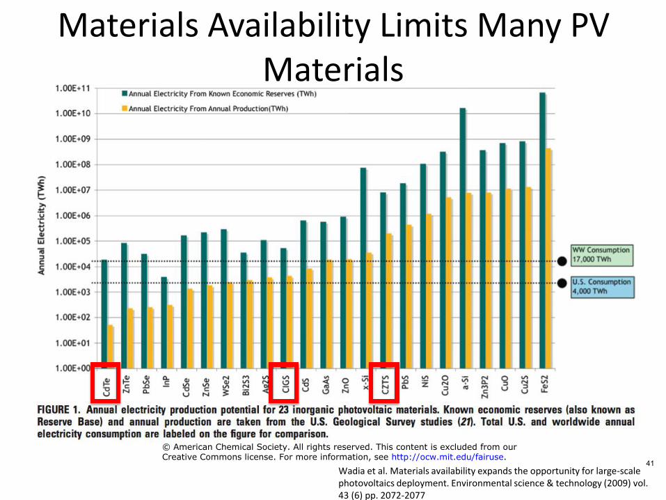
Wadia et al. Materials availability expands the opportunity for large-scale photovoltaics deployment. Environmental science & technology (2009) vol. 43 (6) pp. 2072-2077
Materials Availability Limits Many PV Materials
© American Chemical Society. All rights reserved. This content is excluded from ourCreative Commons license. For more information, see http://ocw.mit.edu/fairuse.
41
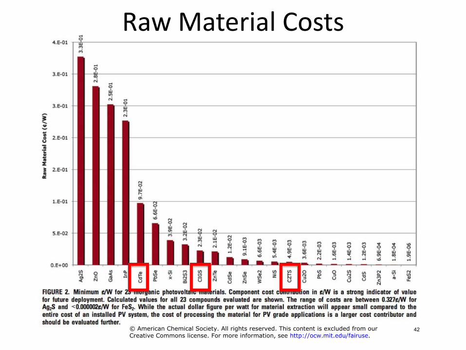
Raw Material Costs
© American Chemical Society. All rights reserved. This content is excluded from ourCreative Commons license. For more information, see http://ocw.mit.edu/fairuse.
42
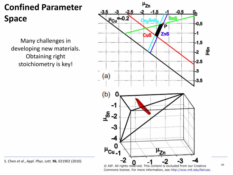
Confined Parameter Space
Many challenges in developing new materials
Obtaining right stoichiometry is key!
.
S. Chen et al., Appl. Phys. Lett. 96, 021902 (2010) 43
© AIP. All rights reserved. This content is excluded from our CreativeCommons license. For more information, see http://ocw.mit.edu/fairuse.
© AIP. All rights reserved. This content is excluded from our CreativeCommons license. For more information, see http://ocw.mit.edu/fairuse.
MIT OpenCourseWarehttp://ocw.mit.edu
2.627 / 2.626 Fundamentals of PhotovoltaicsFall 2013
For information about citing these materials or our Terms of Use, visit: http://ocw.mit.edu/terms.