Embed Size (px)
Citation preview
ADRF6620-EVALZ User Guide UG-558
One Technology Way • P.O. Box 9106 • Norwood, MA 02062-9106, U.S.A. • Tel: 781.329.4700 • Fax: 781.461.3113 • www.analog.com
Evaluating the ADRF6620, a 700 MHz to 2700 MHz Rx Mixer
with Integrated IF Amplifier, Fractional-N PLL, and VCO
PLEASE SEE THE LAST PAGE FOR AN IMPORTANT WARNING AND LEGAL TERMS AND CONDITIONS. Rev. 0 | Page 1 of 16
FEATURES Full-featured evaluation board for the ADRF6620 On-board USB for SPI control Single +5 V operation C# software interface for serial port control
EVALUATION KIT CONTENTS ADRF6620 evaluation board USB cable
ADDITIONAL EQUIPMENT NEEDED Analog signal sources Power supply (6.0 V, 2.5 A) PC running Windows® 98 (2nd ed.), Windows 2000,
Windows ME, Windows XP, or Windows 7 USB 2.0 port, recommended
SOFTWARE NEEDED ADRF6620 control software
ONLINE RESOURCES ADRF6620 data sheet ADRF6620-EVALZ user guide
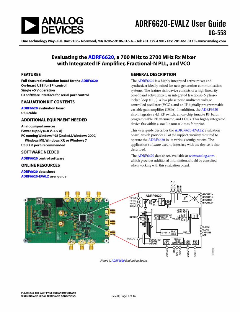
GENERAL DESCRIPTION The ADRF6620 is a highly integrated active mixer and synthesizer ideally suited for next generation communication systems. The feature rich device consists of a high linearity broadband active mixer, an integrated fractional-N phase-locked loop (PLL), a low phase noise multicore voltage controlled oscillator (VCO), and an IF digitally programmable variable gain amplifier (DGA). In addition, the ADRF6620 also integrates a 4:1 RF switch, an on-chip tunable RF balun, programmable RF attenuator, and LDOs. This highly integrated device fits within a small 7 mm × 7 mm footprint.
This user guide describes the ADRF6620-EVALZ evaluation board, which provides all of the support circuitry required to operate the ADRF6620 in its various configurations. The application software used to interface with the device is also described.
The ADRF6620 data sheet, available at www.analog.com, which provides additional information, should be consulted when working with this evaluation board.
LOCK_DETVPTATSCAN
LOIN–
VTUNE
ADRF6620
LOIN+
÷1, ÷2,÷4, ÷8CHARGE
PUMPCP
N = INT +
REFIN
MUXOUT
RFIN0IFOUT1–
MXO
UT+
CS
SCLK
SDIO
DEC
L1
DEC
L4
DEC
L2
MXO
UT–
IFIN
+IF
IN–
LOIN+LOIN–VTUNECP
SERIALPORT
INTERFACELDOVCO
LDO3.3V
IFOUT1+IFOUT2–IFOUT2+
LDO2.5 V
RFIN1RFIN2RFIN3
÷2
÷8÷4÷2×1×2
+PFD
FRACMOD
1149
3-00
1
Figure 1. ADRF6620 Evaluation Board

UG-558 ADRF6620-EVALZ User Guide
Rev. 0 | Page 2 of 16
TABLE OF CONTENTS Features .............................................................................................. 1 Evaluation Kit Contents ................................................................... 1 Additional Equipment Needed ....................................................... 1 Software Needed ............................................................................... 1 Online Resources .............................................................................. 1 General Description ......................................................................... 1 Revision History ............................................................................... 2 Evaluation Board Hardware ............................................................ 3
Introduction .................................................................................. 3 Power Supply ................................................................................. 3
RF Inputs ........................................................................................3 LO Input/Output ...........................................................................3 Mixer Output .................................................................................4 IF Variable Gain Amplifier ..........................................................5
Evaluation Board Control Software ................................................6 Software Requirements .................................................................6 ADRF6620 Evaluation Software ..................................................6
Schematics and Artwork ..................................................................9 Bill of Materials ............................................................................... 13
REVISION HISTORY 8/13—Revision 0: Initial Version

ADRF6620-EVALZ User Guide UG-558
Rev. 0 | Page 3 of 16
EVALUATION BOARD HARDWARE INTRODUCTION The ADRF6620 evaluation board provides all of the support circuitry required to operate the ADRF6620 in its various modes and configurations. Figure 2 shows the typical bench setup used to evaluate the performance of the ADRF6620.
POWER SUPPLY The ADRF6620 evaluation board requires a single +5 V power supply. Connect the positive power terminal to one of the red test loops, either VCC1 or VCC2. The ADRF6620 consumes less than 400 mA at power up with the default register settings.
RF INPUTS The high isolation 4:1 RF switch and on-chip tunable RF balun enables the ADRF6620 to support four single-ended 50 Ω terminated RF inputs. The 4:1 RF switch can be controlled serially via the SPI port or parallel control using switches S1 and S2. The default configuration is parallel control using the switches. The operational frequency range of the RF inputs is from 700 MHz to 2700 MHz and the inputs should be ac-coupled.
LO INPUT/OUTPUT The ADRF6620 offers two alternatives for generating the differential LO input signal: externally via a high frequency low phase noise LO signal or internally via the on-chip Fractional-N synthesizer. In either case, the differential LO signal can be routed off chip to the SMA connector labeled LO_Output.
For internal LO configuration using the on-chip Fractional-N synthesizer, apply a low phase noise reference signal to the REFIN connector. The PLL reference input can support a wide frequency range since the division or multiplication blocks can be used to increase or decrease the reference frequency to the desired value before it is passed to the phase frequency detector (PFD). The integrated synthesizer enables continuous LO coverage from 350 MHz to 2850 MHz.
For optimum performance using an external LO source, the LO inputs, LOIN and LOIP, should be driven differentially. Unless an ac-coupled balun/transformer is used to generate the differential LO, the inputs must be ac-coupled. The input impedance of the differential LO signals is 50 Ω.
IF AMP OUTPUTPLL REF INPUT
LO OUTPUT
MIXER OUTPUT
IF AMP INPUT
USB CONNECTIONTO COMPUTER
RFINPUTS
EXTERNALLO INPUT
+5V POWERSUPPLY
1149
3-00
2
Figure 2. ADRF6620 Typical Measurement Setup

UG-558 ADRF6620-EVALZ User Guide
Rev. 0 | Page 4 of 16
MIXER OUTPUT The mixer outputs of the ADRF6620 are routed off chip for external biasing and optional low-pass filtering. The output pins, MXOP and MXON, require supply biasing to +5 V and the mixer’s differential output impedance is approximately 255 Ω. Refer to the ADRF6620 data sheet for the equivalent mixer output impedance and recommendations on the inter-stage filter design. The default configuration of the evaluation board has the mixer outputs ac-coupled to the IF VGA inputs.
The ADRF6620 evaluation board provides the option to monitor the front-end of the ADRF6620 independently from the variable gain IF amplifier by routing the differential mixer outputs to the SMA connectors. To achieve this configuration, remove L5 and L6 and populate C65 and C66 with 0.1 µF. The MXOP and MXON pins are routed to a 4:1 impedance
transformer from Mini-Circuits, TC4-1W+, to translate the 250 Ω output impedance of the mixer to 50 Ω (see Figure 3).
Attention needs to be paid to the IF frequency of the mixer output and the bandwidth of the transformer. The 1 dB band-width of the TC4-1W+ is limited to 100 MHz and the 3 dB band is 800 MHz. Alternatively, the 4:1 impedance transformer can be replaced with a 1:1 transformer, such as the TC1-1-13M+, and the L-resistor network (R33, R34, R32, and R10) can be used for impedance matching. The tradeoff to this approach is that the L-network is essentially a voltage divider that results in power loss.
If using a 1:1 transformer, populate R32 = R33 = 113 Ω and R34 = R10 = 28 Ω. This configuration results in a voltage loss of −19.6 dB.
C66
C65 R33
0ΩR0402
R32
0ΩR0402
5 4 3 2
1 MXOUT
MXON
MXOP
0.1µF
0.1µF
AGND
AGND
DNI
DNI
AGNDAGND
R10R0402DNI
AGND
R34R0402DNI
T1TC4–1W+
C680.1µFC0402
1149
3-00
3
Figure 3. Mixer Output Schematic

ADRF6620-EVALZ User Guide UG-558
Rev. 0 | Page 5 of 16
IF VARIABLE GAIN AMPLIFIER The final IF amplifier stage amplifies the mixer outputs by 3 dB to 15 dB in 0.5 dB steps. The default configuration of the evaluation board has the mixer outputs routed to the IF amp inputs, however the evaluation board offers the flexibility of isolating the IF amp independently. To evaluate the amplifier independently of the mixer, remove C18 and C19 and populate C70 and C71 with 0.1 µF.
By design, the IF amplifier has been optimized for OIP3 when the source and load impedance are terminated with 150 Ω. This matched condition can be achieved by using 3:1 impedance transformers at both the IF amplifier’s input and output (see Figure 4 and Figure 5). The 50 Ω source
impedance of the signal generator will reflect as 150 Ω at the IF amplifier’s input after the TCM3-1T+.
This same principle also holds true for the amplifier’s output where the spectrum analyzer’s impedance translates to 150 Ω after the transformer. If the IF amplifier is to be terminated with a source or load impedance different from what an impedance transformer can offer, a 1:1 transformer and matching network can be used.
If the load or the source resistance is not equal to 150 Ω, refer to the ADRF6620 data sheet for equations which can be used to determine the resulting gain and input/output resistances.
1
23
6
4
AGNDAGND
IFIN
C71
C70R40
0ΩR0402
R41
0ΩR0402
5432
1
IFIP
IFIN
0.1µFC0402
0.1µFC0402
AGND
AGND
R38R0402DNI
AGND
R37R0402DNI
T5TCM3–1T+
C690.1µFC0402
1149
3-00
4
Figure 4. IF Amplifier Input Schematic
AGND
AGND
AGND
AGND
AGND AGND
DNIR51
0Ω
1
23
6
4
R480ΩR25
33ΩDNI
R3933ΩDNI R49
0Ω
AGNDT2TCM3–1T+
C120.1µF
C0402
C70.1µFC0402
C80.1µFC0402
C640.1µF
C0603
C630.1µFC0603
DNIR50
0Ω
R35
0Ω
R36
0Ω
DNIR56
0ΩR520Ω
R200ΩDNI
R190ΩDNI
5 4 3 2
1 IFOUT+
5 4 3 2
1 IFOUT–
50Ω SEIFOUT+
IFOUT–
FILTER–
FILTER+
L11µH
L0805
L21µHL0805
VCC
IFOUT+
75Ω SE150Ω DIFFERENTIAL
IFOUT–
1149
3-00
6
Figure 5. IF Amplifier Output Schematic

UG-558 ADRF6620-EVALZ User Guide
Rev. 0 | Page 6 of 16
EVALUATION BOARD CONTROL SOFTWAREThe ADRF6620 evaluation board is configured with a USB-friendly interface to allow programmability of the ADRF6620 registers.
SOFTWARE REQUIREMENTS These instructions describe how to install the ADRF6620 control software, as well as the Cypress generic USB driver, onto a Windows XP, Vista, or Windows 7 computer running either a 32-bit or 64-bit operating system. Install the necessary software before plugging the USB cable to the computer.
1. In the extracted folder, ADI_RFG_Drivers, run the ADI_RFG_Drivers.exe file. Running this file allows the installation of the Cypress CyUSB.sys driver as a verified, signed driver.
2. Run the file ADRF6620_install.exe from the extracted .zip file. An icon should appear on your desktop with the Analog Devices, Inc., logo, labeled ADRF6620.
3. Install the USB driver once the installer is finished. Plug the RFG USB adapter into the PC using a USB cable.
4. In either Windows XP or Vista, right click on My Computer and select Properties. Next, in Vista or Windows 7, select the Device Manager option. In XP, select the hardware tab and then Device Manager.
5. In Device Manager, select the last category, Universal Serial Bus Controllers. There will be an entry with either a yellow flag (for unknown device) or ADF4xxx USB Driver (if you have installed the previous ADRF6x0x or Analog Devices Limerick PLL software). Right click on this device and select update driver. Browse to select the directory C:\Program Files\ADRF6620_customer_software.
6. Click Next to complete the driver installation successfully.
ADRF6620 EVALUATION SOFTWARE The ADRF6620 evaluation software offers a block diagram view of how the registers affect the major functional blocks of the ADRF6620. The main screen of the evaluation software is shown in Figure 6.
Before reading or writing to the registers, validate the USB connection by reading the USB indicators at the lower left corner of the software. The DUT to GUI button reads the register values from the device and updates the user interface. An automatic write to the chip is initiated every time a register value is changed from the user interface.
The PLL synthesizer blocks perform background calculations; the user need only specify the PLL reference and desired LO frequency and the software calculates and sets the INT, FRAC, and MOD values accordingly. The green boxes require user input while the yellow boxes are read only.
The Engineering tab, as shown in Figure 7, allows specific reads and writes to the individual registers. Decimal format is required when entering data to the address and data fields.

ADRF6620-EVALZ User Guide UG-558
Rev. 0 | Page 7 of 16
USB CONNECTION INDICATOR
INPUT PLLREFERENCE
PFD FREQAUTOMATICALLYCALCULATED
SYNTHESIZER VALUESAUTOMATICALLYCALCULATED
INPUTDESIREDLO FREQ
INCREMENT ORDECREMENT LO
FREQ BY STEP SIZEVCO FREQ
AUTOMATICALLYCALCULATED
READS REGISTERSFROM .TXT FILE
WRITE REGISTERSTO .TXT FILE
READS VALUES FROMDUT AND UPDATESTHE INTERFACE 11
493-
007
Figure 6. Main Screen of the ADRF6620 Control Software with Default Power-Up Settings

UG-558 ADRF6620-EVALZ User Guide
Rev. 0 | Page 8 of 16
1149
3-00
8
Figure 7. Engineering Tab of the ADRF6620 Control Software

ADRF6620-EVALZ User Guide UG-558
Rev. 0 | Page 9 of 16
SCHEMATICS AND ARTWORK
REPLACE WITH NEW 0603CS
SHARE PADS
0.1UFC0402
C3 C14 SDIO
TBD0603
C82
TBD0603
L9
49.9
3435
RFSW1
C11
13V3_XTAL
2
6
4 3
1
T4
2
6
4 3
1
T3
R59
C73
6
4
513
2
Y2
23
1JP1
23 1
S2
23 1
S1
C86
C85
C83
C81
L14
L13
C78
R68
L42
1
L3
5 4 3 2
1LOIN+
R57
R58
R67
L12
C84
L11
L10L8R66
C79
L7R65
C76
C75
L6
L5
C19
C18
C62C61
R16
R15
C67 C72
C23
C22
5 4 3 2
1LOIN-
VCC1
C15
1
VCC2
C17
C9 C13 C16
1DCL_VCO
C29
C54
C2
1DECL_2P5
C6
C5C1
1DECL_3P3
C42
5 4 3 2
1RF3
C41
5 4 3 2
1RF2
C40
5 4 3 2
1 RF1
C32
5 4 3 2
1 RF0
5432
1REFIN R4
C10
241413
12
14047 42 41 3 9 38
26
29
326
PAD
191843
2221
4445
1110
98
15 16
48
36
33
3130
2827
25
232017
54
46 37
7
23
U4
C21C20
1DECL_LO
A C
CR3R9
1VTUNE1
CP_OUT
1GND4
1GND3
1GND2
1GND1
C26 C27
5 4 3 2
1 LOOUT+C25
C24
R11
1
MUXOUT
C43C30C28
R28
R27
R29
C57 C60C59
C58
R23
R12
R26
RED
RED
TC1-1-43A+
LOON
LOOP
100PF
LOIP
LOIN0.1UF 100PF
TBD0402
TBD0603
TBD0402DNI
TC1-1-43A+
100PF
0
3V3_USB
3PIN_SOLDER_JUMPER
100PF
CPOUT
100PF
0
0
C0402
38.4MEGHZ
C0402
100PF
YEL
10UFC0402C0402
TBD0402
0.1UF
100PF
CSB
TBD0402MXOP
MXON
VCCTBD0402
DNITBD0402
0 ohms
0 ohms
TBD0402
VCC
0.1UF
09-03-201-02
RFSW1
09-03-201-02
RFSW0
100PF
3K
22PF
10K
6.8PF
10K
2700PF
22PF
0
DECL_VCO
0.1UF
0 0
VCC
39NH
39NH
150PF
LOIP
YELRFSW0
RFIN0
100PF
SCLK
1.00K
100PF
RFIN3
RFIN2
RFIN1
0.1UF
100PF
0.1UF
ADRF6620ACPZVCC
0.1UF
100PF0.1UF
100PF
LOIN-
LOIN+
DNI
DNI
0.1UF
SML-210MTT86
IFIP
IFIN
470NH
IFIPIFIN
VCC
YEL
DNI
DNI
TBD0603DNI
DNI
TBD0603DNI
DNI
DNI
VCC
TBD0603DNIDNI
0.1UF
100PF
VCC
0.1UF
C0402
YEL
VCC
100PF
VCC
DECL_VCO
C04020.1UF
YEL
100PF
10UF
YEL
RED
100PFC0402
0.1UF
10UF
BLKBLKBLKBLK
0.1UF
150PF
0
YEL
DNITBD0402
0
100PF
CPOUT VTUNE
TBD0402
0DNI
470NH
DNI0
0
C0402VTUNE
0100PF
IFONIFOP
LOIN
BCOM
A
PAD
GND
VTUN
EDE
CL4
LOIN
+LO
IN-
MUX
OUT
SDIO
SCLK CS
BRF
S W1
R FSW
0DE
CL3
GNDRFIN0
GNDGND
RFIN1GNDGND
RFIN2GNDGND
RFIN3GND
VPOS
5GN
DLO
OUT-
LOOU
T+GN
DM
XOUT
-M
X OUT
+G N
DIF
IN+
I FIN
-VP
OS4
VPOS
3
VPOS2IFOUT2-IFOUT2+IFOUT1-IFOUT1+DECL2REFINGNDGNDCPDECL1VPOS1
ENABLE/DISABLE_N
VCC
NC
OUTPUT
GND
NC
SECPRI
NC
SECPRI
1149
3-01
1
Figure 8. Schematic

UG-558 ADRF6620-EVALZ User Guide
Rev. 0 | Page 10 of 16
R34=DNI
R10=DNI
R33=0 OHMS
R32=0 OHMS
TC4-1W+
R34=28 OHMS
R33=113 OHMS
R10=28 OHMS
TC1-1-13M+
150 OHM DIFFERENTIAL
75 OHM SE
R32=113 OHMS
50 OHM SE
R56
5 4 3 2
1 B_IFOUT-
5 4 3 2
1 B_IFOUT+
R20
R19
R31
R30
L16
L15
C77
L18
L17
C80
L20
L19
R36
R35
1
2
3
6
4
T2
1
2
3
6
4
T5
C66
C65
R50
R52R48
R51
R49
R37
R38
R40
R41
R10
5 4 3 2
1 IFOUT-
R39
5432
1IFIN
C69
C71
C70
C68
R34
C12
R33
R32
T1
C64 C63L1
5 4 3 2
1 MXOUT
L2
C7
C8
R255 4 3 2
1 IFOUT+
DNI
DNIDNI
DNI
DNI
IFOUT-
IFOUT+
0
DNI
00
L0805 L0805
TCM3-1T+
24NH
DNI
DNI
24NH
FILTER-
0.1UF
0.1UF
0 0.1UF
FILTER+
IFIN
IFIP
MXOP
MXON
0.1UF
0.1UF
R0402
C06030.1UF
0
FILTER-
FILTER+
DNIDNI
DNI
1.8PF2PF
24NHDNI
0.1UFC0402
75
75
033
DNI
0
C0402
0
TCM3-1T+ C0402
TBD0402
R0402DNI
R0402
DNI
TBD0402
C0402
R04020
C0402
0.1UF1UH
R0402
DNI
DNI
R04020
VCC
DNI
0
0
0
24NH 24NH
C0402
TBD0402
0
DNI
R0402
TC4-1W+
DNI
TBD0402
0.1UF R0402
C0603
C04020.1UF
24NHDNI
DNI
DNI
1UH
DNI
0.1UF
IFOP
IFON
33
DNI
1149
3-01
2
IF AMP OUTPUT
MIXER OUTPUT
IF AMP INPUT
Figure 9. Mixer Output and IF Amplifier Input/Output Schematics

ADRF6620-EVALZ User Guide UG-558
Rev. 0 | Page 11 of 16
330PF
PLACEHOLDER
330PF330PF
DECOUPLING FOR U1
R 46
A C
CR2R8R55
R24
R54
R53
C53 R13 C55 R14 C56
10987654321
P3
4
5
44
5543322 7171 1
1615
42
14
21
52515049484746452524232221201918
PAD
4039383736353433
13
565341282 612
89
31302954
73106
U1
C35 C36 C38 C39 C45 C46 C48
R45A C
D1
R1 C376
PAD
21
87
5
3
U3
R3
C44 R2 C47
7
8
56
4
321
U2 R5
C49 C34
R47 R7
C31
C50
54321
G4G3G2G1
P1
C51
31
42
Y1
C52
C33
C4
SCL
SDA
CTL2_FLAGC
PA0
ADP3334ACPZ
3V3_USB
140K
2K
PA1
PA2
SML-210MTT86
5V_USB
5V_USB
0
1.00K
24.000000MEGHZ
DNI
TBD0603100K
1UF
1UF
WAKEUP
DM
0.1UF
XTALOUT
22PF
DNI
TBD0402 TBD0402
DNI
0
0
DNI
0.1UF
10PF
DP
E013815
FB
1000PF
78.7K
2K
SML-210MTT86
0.1UF0.1UF 0.1UF 0.1UF 0.1UF 0.1UF
TSW-105-08-G-DDNI
2K
0
0.1UF 0.1UF
DNI
1.00KDNI
1.00KDNI
22PF
XTALIN
897-43-005-00-100001
3V3_USB
2K
CLKOUT
PA3
PA4
PA5
PB1
PB0
PB4
PB3
PB2
PB5
PD1
PD0
PD3
PD6
PD5
PD4
PD7
DGND
DGNDDGND
DGND
DGND
DGND
DGND
DGND
DGND
CTL1_FLAGB
JEDEC_TYPE=QFN56_8X8_PAD5_2X4_5
CY7C68013A-56LTXC
RESETN
PD2
PA7
10PF
0.1UF
24LC64-I-SN
CTL0_FLAGA
PB6
PB7
CSB
SDIO
SCLK
TBD0402
IFCLK
PA6
OUT
OUT
OUT
PINSGND
OUT
CASE
PAD
CLKOUT
PD7_FD15
PD6_FD14
PD5_FD13
PD4_FD12
PD3_FD11
PD2_FD10
PD1_FD9
PD0_FD8
W AKEUP
RESET_N
PA7_FLAGD_SLCS_N
PA6_PKTEND
PA5_FIFOADR1
PA4_FIFOADR0
PA3_W U2
PA2_SLOE
PA1_INT1_N
PA0_INT0_N
VCC
CTL2_FLAGC
CTL1_FLAGB
CTL0_FLAGA
GND
PB7_FD7
PB6_FD6
PB5_FD5
PB4_FD4
PB3_FD3
PB2_FD2
PB1_FD1
PB0_FD0
SDA
SCL
RESERVED
IFCLK
DMINUS
DPLUS
AGND
XTALIN
XTALOUTAVCC
RDY1_SLW R
RDY0_SLRD
IO
IN1
IN2 OUT2
OUT1
PADFB
GNDSD_N
GND
SCL SDA
W C_N
A2
A1
A0VCC
IN
IN
OUT
OUT
OUT
OUT
OUT
OUT
OUT
OUT
OUT
OUT
OUT
OUT
OUT
OUT
OUT
OUT
OUT
OUT
OUT
OUT
OUT
OUT
OUT
OUT
OUT
USB: SERIAL CONTROL
1149
3-01
3
Figure 10. USB Serial Control

UG-558 ADRF6620-EVALZ User Guide
Rev. 0 | Page 12 of 16
1149
3-00
9
Figure 11. Primary Side Layout
1149
3-01
0
Figure 12. Secondary Side Layout

ADRF6620-EVALZ User Guide UG-558
Rev. 0 | Page 13 of 16
BILL OF MATERIALS Table 1. Qty Reference Designator Description Tolerance Voltage Manufacturer Part Number 3 VCC1, VCC2, 3V3_XTAL Conn-PCB test point, red Components
Corp TP-104-01-02
8 VTUNE, 5V_SDP, CP_OUT, MUXOUT, DCL_VCO, DECL_LO, DECL_2P5, DECL_3P3
Conn-PCB test point, yellow Components Corp
TP-104-01-04
3 C1, C9, C43 Cap cer, X5R 0603, 10 µF 20 6.3 V Murata GRM188R60J106ME47D
13 C6, C10, C11, C16, C22 to C25, C28, C32, C40 to C42
Cap chip mono cer, C0G 0402, 100 pF
5 50 V Murata GRM1555C1H101JD01D
27 C2 ,C5, C7, C8, C12, C13, C18, C19, C30, C31, C33 to C36, C38, C39, C45, C46, C48, C49, C61, C62, C68 to C71, C73
Cap cer, X7R 0402, 0.1 µF 10 16 V Murata GRM155R71C104KA88D
6 C14, C17, C27, C29, C54, C67 Cap cer, NP0, 0805, 100 pF 5 100 V AVX 08051A101JAT2A
6 C3, C15, C26, C72, C75, C76 Cap cer, X7R 0603, 0.1 µF 10 50 V AVX 06035C104KAT2A
2 C20, C21 Cap cer, C0G 0402, 150 pF 5 50 V Murata GRM1555C1H151JA01D
2 C37, C47 Cap mono cer, X5R, 0603, 1 µF 10 25 V Murata GRM188R61E105KA12D
2 C4, C50 Cap cer, multilayer NP0 0402, 10 pF
5 50 V PHYCOMP (YAGEO)
CC0402JRNP09BN100
1 C44 Cap cer, C0G 0603, 1000 pF 5 100 V TDK C1608C0G2A102J
4 C51, C52, C57, C60 Cap cer, NP0, 0603, 22 pF 5 50 V PHYCOMP (YAGEO)
CC0603JRNP09BN220
1 C58 Cap cer, C0G 0603, 2700 pF 5 50 V Murata GRM1885C1H272JA01D
1 C59 Cap cer, NP0, 0603, 6.8 pF 5 50 V PHYCOMP (YAGEO)
2238 867 15688
2 C63, C64 Cap cer, CHIP X8R, 0603, 0.1 µF 10 25 V TDK C1608X8R1E104K
2 C81 ,C83 Cap cer, 0402 C0G, 1.6 pF 0.1 pF 50 V Murata GJM1555C1H1R6BB01B
2 C85, C86 Cap cer, C0G SMD, 0402, 2 pF ±0.25 pF 50 V Murata GJM1555C1H2R0CB01D
3 D1, CR2, CR3 LED 570 NM WTR CLR, 0805, SMD (green)
N/A 2.2 V Rohm SML-210MTT86
4 GND1 to GND4 Conn-PCB test point, black Components Corp
TP-104-01-00
10 RF0 to RF3, IFIN, MXOUT, REFIN, IFOUT+, IFOUT−, LOOUT+
Conn-PCB coax SMA end launch
Johnson 142-0701-851
2 L1, L2 Inductor SM, 0805, 1 µH 5 Coilcraft 0805LS-102XJLB
2 L3, L4 Inductor SM, 0603, 470 nH 5 Coilcraft 0603LS-471XJLC
2 L5, L6 Inductor SM, 7144, 39 nH 5 Coilcraft 0603CS-39NXJLU
2 LOIN+ ,LOIN− Conn-PCB coax SMA ST Johnson 142-0701-201
1 P1 Conn-PCB recept mini-USB Type B SMT
Mill-Max 897-43-005-00-100001
1 P2 Conn-PCB vert type rcpt SMD HRS FX8-120S-SV(21)
4 R1, R5, R8, R45 Res, film SMD 0603, 2 K, 1/10 W
1 PHYCOMP (YAGEO)
9C06031A2001FKHFT
23 R11, R15, R16, R22, R24, R28, R29, R32, R33, R35, R36, R40, R41, R46, R48, R49, R52 to R54, R57 to R59, R67, L13, L14
Res, film SMD 0402, 0, 1/16 W 5 Panasonic ERJ-2GE0R00X
1 R12 Res, thick film chip, 0402, 3 K, 1/16 W
5 Panasonic ERJ-2GEJ302X
3 R18, R44, R47 Res, prec thick film chip, 0603, 100 K, 1/10 W
1 50 V Panasonic ERJ-3EKF1003V
1 R2 Res, prec thick film chip, 0603, 140 K, 1/10 W
1 50 V Panasonic ERJ-3EKF1403V
2 R23, R26 Res, prec thick film chip, 0402, 10 K, 1/16 W
1 Panasonic ERJ-2RKF1002X
1 R3 Res, prec thick film chip, 0603, 78.7 K, 1/10 W
1 50 V Panasonic ERJ-3EKF7872V
1 R4 Res, prec thick film chip, 0402, 49.9 K, 1/16 W
1 Panasonic ERJ-2RKF49R9X

UG-558 ADRF6620-EVALZ User Guide
Rev. 0 | Page 14 of 16
Qty Reference Designator Description Tolerance Voltage Manufacturer Part Number 1 R9 Res, prec thick film chip, 0402,
100 K, 1/10 W 1 Panasonic ERJ-2RKF1001X
2 S1, S2 SW PCB mount slide SECMA 09-03-201-02
1 T1 XFMR RF, 0.25 W Mini circuits TC4-1W+
2 T2, T5 XFMR RF, 0.25 W Mini circuits TCM3-1T+
2 T3, T4 XFMR RF, SMT Mini-circuits TC1-1-43A+
1 U1 IC HS USB peripheral 3 V to 3.6 V
Cypress Semiconductor
CY7C68013A-56LTXC
1 U2 IC 64 K bit EEPROM Microchip 24LC64-I-SN
1 U3 IC-ADI high acc. low IQ adj low drop reg
Analog Devices ADP3334ACPZ
1 U4 IC Rx mixer, fractional-N PLL and VCO
Analog Devices ADRF6620ACPZ
1 U5 IC 32 K bit serial EEPROM Microchip 24LC32A-I/MS
1 Y1 IC crystal SMD NDK NX3225SA-24.000000MHZ
1 Y2 IC crystal osc, 38.4 MHz 3.3 V

ADRF6620-EVALZ User Guide UG-558
Rev. 0 | Page 15 of 16
NOTES

UG-558 ADRF6620-EVALZ User Guide
Rev. 0 | Page 16 of 16
NOTES
ESD Caution ESD (electrostatic discharge) sensitive device. Charged devices and circuit boards can discharge without detection. Although this product features patented or proprietary protection circuitry, damage may occur on devices subjected to high energy ESD. Therefore, proper ESD precautions should be taken to avoid performance degradation or loss of functionality.
Legal Terms and Conditions By using the evaluation board discussed herein (together with any tools, components documentation or support materials, the “Evaluation Board”), you are agreeing to be bound by the terms and conditions set forth below (“Agreement”) unless you have purchased the Evaluation Board, in which case the Analog Devices Standard Terms and Conditions of Sale shall govern. Do not use the Evaluation Board until you have read and agreed to the Agreement. Your use of the Evaluation Board shall signify your acceptance of the Agreement. This Agreement is made by and between you (“Customer”) and Analog Devices, Inc. (“ADI”), with its principal place of business at One Technology Way, Norwood, MA 02062, USA. Subject to the terms and conditions of the Agreement, ADI hereby grants to Customer a free, limited, personal, temporary, non-exclusive, non-sublicensable, non-transferable license to use the Evaluation Board FOR EVALUATION PURPOSES ONLY. Customer understands and agrees that the Evaluation Board is provided for the sole and exclusive purpose referenced above, and agrees not to use the Evaluation Board for any other purpose. Furthermore, the license granted is expressly made subject to the following additional limitations: Customer shall not (i) rent, lease, display, sell, transfer, assign, sublicense, or distribute the Evaluation Board; and (ii) permit any Third Party to access the Evaluation Board. As used herein, the term “Third Party” includes any entity other than ADI, Customer, their employees, affiliates and in-house consultants. The Evaluation Board is NOT sold to Customer; all rights not expressly granted herein, including ownership of the Evaluation Board, are reserved by ADI. CONFIDENTIALITY. This Agreement and the Evaluation Board shall all be considered the confidential and proprietary information of ADI. Customer may not disclose or transfer any portion of the Evaluation Board to any other party for any reason. Upon discontinuation of use of the Evaluation Board or termination of this Agreement, Customer agrees to promptly return the Evaluation Board to ADI. ADDITIONAL RESTRICTIONS. Customer may not disassemble, decompile or reverse engineer chips on the Evaluation Board. Customer shall inform ADI of any occurred damages or any modifications or alterations it makes to the Evaluation Board, including but not limited to soldering or any other activity that affects the material content of the Evaluation Board. Modifications to the Evaluation Board must comply with applicable law, including but not limited to the RoHS Directive. TERMINATION. ADI may terminate this Agreement at any time upon giving written notice to Customer. Customer agrees to return to ADI the Evaluation Board at that time. LIMITATION OF LIABILITY. THE EVALUATION BOARD PROVIDED HEREUNDER IS PROVIDED “AS IS” AND ADI MAKES NO WARRANTIES OR REPRESENTATIONS OF ANY KIND WITH RESPECT TO IT. ADI SPECIFICALLY DISCLAIMS ANY REPRESENTATIONS, ENDORSEMENTS, GUARANTEES, OR WARRANTIES, EXPRESS OR IMPLIED, RELATED TO THE EVALUATION BOARD INCLUDING, BUT NOT LIMITED TO, THE IMPLIED WARRANTY OF MERCHANTABILITY, TITLE, FITNESS FOR A PARTICULAR PURPOSE OR NONINFRINGEMENT OF INTELLECTUAL PROPERTY RIGHTS. IN NO EVENT WILL ADI AND ITS LICENSORS BE LIABLE FOR ANY INCIDENTAL, SPECIAL, INDIRECT, OR CONSEQUENTIAL DAMAGES RESULTING FROM CUSTOMER’S POSSESSION OR USE OF THE EVALUATION BOARD, INCLUDING BUT NOT LIMITED TO LOST PROFITS, DELAY COSTS, LABOR COSTS OR LOSS OF GOODWILL. ADI’S TOTAL LIABILITY FROM ANY AND ALL CAUSES SHALL BE LIMITED TO THE AMOUNT OF ONE HUNDRED US DOLLARS ($100.00). EXPORT. Customer agrees that it will not directly or indirectly export the Evaluation Board to another country, and that it will comply with all applicable United States federal laws and regulations relating to exports. GOVERNING LAW. This Agreement shall be governed by and construed in accordance with the substantive laws of the Commonwealth of Massachusetts (excluding conflict of law rules). Any legal action regarding this Agreement will be heard in the state or federal courts having jurisdiction in Suffolk County, Massachusetts, and Customer hereby submits to the personal jurisdiction and venue of such courts. The United Nations Convention on Contracts for the International Sale of Goods shall not apply to this Agreement and is expressly disclaimed.
©2013 Analog Devices, Inc. All rights reserved. Trademarks and registered trademarks are the property of their respective owners. UG11493-0-8/13(0)