Embed Size (px)
Citation preview
ADP5091-1-EVALZ/ADP5092-1-EVALZ User Guide UG-967
One Technology Way • P.O. Box 9106 • Norwood, MA 02062-9106, U.S.A. • Tel: 781.329.4700 • Fax: 781.461.3113 • www.analog.com
Evaluation Board for the ADP5091/ADP5092 Ultralow Power Energy Harvesting
PMU
PLEASE SEE THE LAST PAGE FOR AN IMPORTANT WARNING AND LEGAL TERMS AND CONDITIONS. Rev. 0 | Page 1 of 12
GENERAL DESCRIPTION The ADP5091/ADP5092 is a 2-channel ultralow power energy harvesting PMU in a compact 4 mm × 4 mm LFCSP package. The ADP5091-1-EVALZ and ADP5092-1-EVALZ run from input voltages of 0.38 V to 3.3 V and require minimal external components to provide a high efficiency solution with integrated power switches, synchronous rectifier, battery management, and hybrid controlled and regulated output.
The ADP5091-1-EVALZ and ADP5092-1-EVALZ evaluation boards provide an easy way to evaluate the device. This user guide describes how to quickly set up the evaluation board and deliver up to 3.5 V maximum voltage to the SYS output using an external resistor divide. The internal switches turn on as long as the storage element voltage at BAT pin is above the externally programmed SETSD of 2.4 V. The PGOOD indicator toggles high when SYS ramps up to 3 V. The REG_OUT is set to 2.5 V as the default output voltage. Complete information about the ADP5091/ADP5092 is available in the ADP5091/ADP5092 data sheet. Consult the data sheet in conjunction with this user guide when using the evaluation boards.
ADP5091/ADP5092 EVALUATION BOARDS
1444
3-00
1
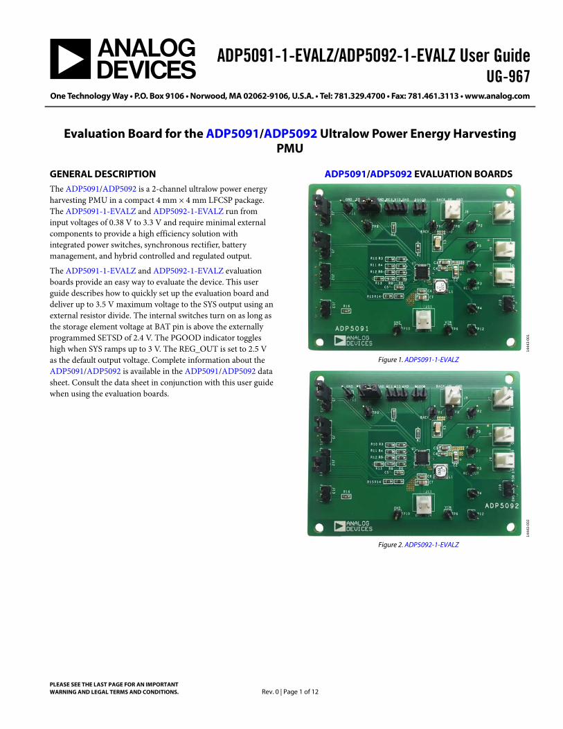
Figure 1. ADP5091-1-EVALZ
1444
3-00
2
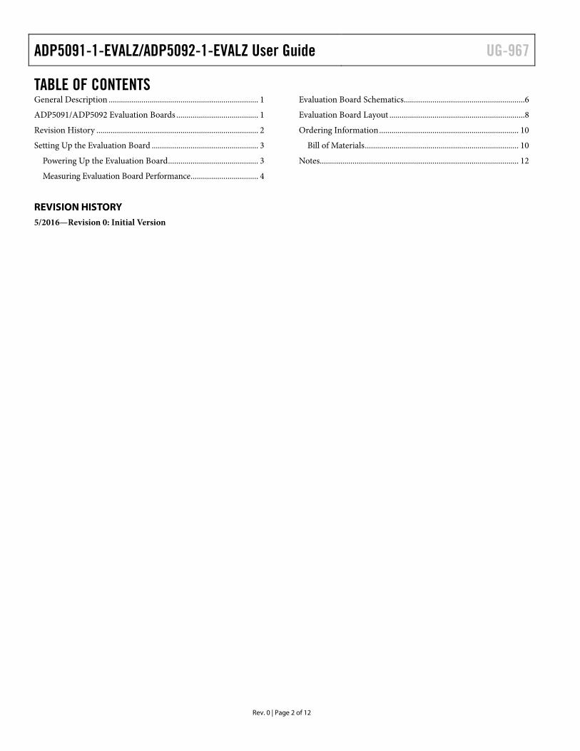
Figure 2. ADP5092-1-EVALZ
ADP5091-1-EVALZ/ADP5092-1-EVALZ User Guide UG-967
Rev. 0 | Page 2 of 12
TABLE OF CONTENTS General Description ......................................................................... 1 ADP5091/ADP5092 Evaluation Boards ........................................ 1 Revision History ............................................................................... 2 Setting Up the Evaluation Board .................................................... 3
Powering Up the Evaluation Board ............................................ 3 Measuring Evaluation Board Performance ................................. 4
Evaluation Board Schematics...........................................................6 Evaluation Board Layout ..................................................................8 Ordering Information .................................................................... 10
Bill of Materials ........................................................................... 10 Notes................................................................................................. 12
REVISION HISTORY 5/2016—Revision 0: Initial Version
UG-967 ADP5091-1-EVALZ/ADP5092-1-EVALZ User Guide
Rev. 0 | Page 3 of 12
SETTING UP THE EVALUATION BOARD POWERING UP THE EVALUATION BOARD The ADP5091-1-EVALZ and ADP5092-1-EVALZ evaluation boards are fully assembled and tested. Before applying power to the evaluation board, follow the setup procedures in this section.
Jumper Settings
Table 1 describes the jumper settings.
Table 1. Jumper Settings.
Jumper State or Connection Function
J1 (DIS_SW)
SYS Disables the main boost GND Enables the main boost
J2 (VID) Floating Set REG_OUT as 2.5 V RES Set output voltage by an external
resistor through VID to ground GND Set output voltage by external
resistor divide at REG_FB pin J3 (REG_D1)
SYS Enable LDO mode of the REG_OUT GND Disable LDO mode of the REG_OUT
J4 (PGOOD)
Pull high when the SYS voltage ramps up to preset the SETPG rising threshold
J5 (REG_D0)
SYS Enable boost mode of the REG_OUT GND Disable boost mode of the REG_OUT
J12 (RDIV)
MPPT With MPPT sensing function Floating Without MPPT dynamic sensing
function, provide an external voltage at CBP pin as MPPT voltage
J13 (FIX MPPT)
Floating Dynamic MPPT sensing mode Connected MPPT fixed mode
Input Power Source Connection
Energy harvesting power sources are high impedance sources. Figure 3 shows that a source meter configured as a current source with a voltage limit set to the open circuit voltage of the harvester is the best way to simulate the harvester. For low output impedance power supply (voltage source), it is necessary to simulate the impedance of the harvester with a physical external resistor (R) between the supply and the VIN pin. If the input current source includes a voltage meter, use the meter to monitor the input voltage as follows:
1. Connect the positive terminal (+) of the power source to the VIN terminal (J11) on the evaluation board.
2. Connect the negative terminal (−) of the power source to the GND terminal (J11) on the evaluation board.
If the input power supply does not include a current meter, connect a current meter in series with the input power supply as follows:
1. Connect the external series resistor of the power source to the positive terminal (+) of the current meter.
2. Connect the negative terminal (−) of the power source to the GND terminal (J10) on the evaluation board.
3. Connect the negative terminal (−) of the current meter to the VIN terminal (J11) on the evaluation board.
SYS Load Connection
Before connecting the load to the ADP5091-1-EVALZ and ADP5092-1-EVALZ evaluation boards, ensure that the SYS voltage is higher than 2 V, or that the power-good signal is high. If the load includes a current meter, or if the current is not measured, connect the load directly to the evaluation board as follows:
1. Connect the positive load connection (+) to the SYS terminal (J9) on the evaluation board.
2. Connect the negative load connection (−) to the GND terminal (J9) on the evaluation board.
If a current meter is used, connect it in series with the load as follows:
1. Connect the positive terminal (+) of the current meter to the SYS terminal (J9) on the evaluation board.
2. Connect the negative terminal (−) of the current meter to the positive terminal (+) of the load.
3. Connect the negative terminal (−) of the load to the GND terminal (J9) on the evaluation board.
Storage Elements Connection
The ADP5091-1-EVALZ and ADP5092-1-EVALZ evaluation boards can charge some types of energy storage elements, such as: rechargeable batteries, super capacitors, and conventional capacitors. In general, the storage elements maintain constant power or peak power of the system that cannot directly come from the input source. It is necessary to consider the significant leakage current of batteries and super capacitors. For the application information, refer to the ADP5091/ADP5092 data sheets.

ADP5091-1-EVALZ/ADP5092-1-EVALZ User Guide UG-967
Rev. 0 | Page 4 of 12
CURRENT SOURCEWITH
VOLTAGE LIMIT
SUPER CAPACITOROR
RECHARGEABLEBATTERY
– +
1444
3-00
3
+
VOLTAGE SOURCE
– +
Figure 3. Setup for the ADP5091-1-EVALZ and ADP5092-1-EVALZ
Input and SYS Voltmeter Connections
Measure the input and SYS voltages with voltmeters. Ensure that the voltmeters connect to the appropriate test points on the board. If the voltmeters are not connected to the correct test points, the measured voltages may be incorrect due to the voltage drop across the leads, or due to the connections between the board, the power source, and/or the load.
1. Connect the positive terminal (+) of the input voltage measuring voltmeter to Test Point TP6 on the evaluation board.
2. Connect the negative terminal (−) of the input voltage measuring voltmeter to Test Point TP10 on the board.
3. Connect the positive terminal (+) of the output voltage measuring voltmeter to Test Point TP5 on the board.
4. Connect the negative terminal (−) of the output voltage measuring voltmeter to Test Point TP7 on the board.
REG_OUT Load Connection
REG_OUT is a regulated output that can be set via the VID pin. REG_D0 and REG_D1 control the operation mode of the REG_OUT. See the detailed configuration in Table 1. If the load includes a current meter, or if the current is not measured, connect the load directly to the evaluation board as follows:
1. Connect the positive load connection (+) to the REG_OUT terminal (J8) on the evaluation board.
2. Connect the negative load connection (−) to the GND terminal (J8) on the evaluation board.
If a current meter is used, connect it in series with the load as follows:
1. Connect the positive terminal (+) of the current meter to the REG_OUT terminal (J8) on the evaluation board.
2. Connect the negative terminal (−) of the current meter to the positive terminal (+) of the load.
3. Connect the negative terminal (−) of the load to the GND terminal (J8) on the evaluation board.
Powering On the Evaluation Board
As long as the input current source open circuit voltage is above a minimum input voltage of cold start (0.38 V), and the input power is above a minimum input power of cold start (6 µW), the ADP5091-1-EVALZ and ADP5092-1-EVALZ enter cold start, if the SYS voltage is lower than end of the cold start-up threshold (1.93 V). Otherwise, the evaluation board enables the main boost instead of the cold start.
When the MPPT sampling circuit is active, the harvester open circuit voltage is detectable because there is no input current to create a drop across the impedance. The main boost runs and draws current until the VIN voltage drops to the sampled MPPT voltage stored at CBP pin.
Optional BACK_UP Setup
An optional primary battery connected to the BACK_UP pin can accelerate the cold start or maintain the system load. When VBAT < VBACK_UP and VBAT < VSET_BK, the ADP5091-1-EVALZ and ADP5092-1-EVALZ turn on the internal power switches between the BACK_UP pin and the SYS pin. When VBAT > VBACK_UP and VBAT > VSET_BK, the internal power switches turn off.
MEASURING EVALUATION BOARD PERFORMANCE Measuring the Switching Waveform
To observe the switching waveform with an oscilloscope, place the oscilloscope probe tip at Test Point TP4 with the probe ground connected to the Test Point TP12 GND Set the oscilloscope to a dc coupling, 2 V/division, 10 µs/division time base. The switching waveform alternates between 0 V and the approximate SYS voltage.
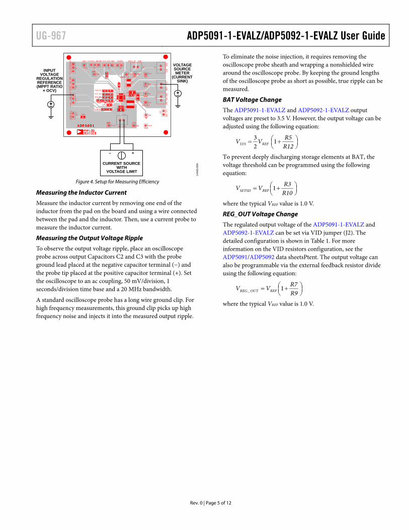
Measuring Efficiency
Measure the efficiency (η) by comparing the input power with the output power. Figure 4 shows the test setup. Float the RDIV jumper (J12) and provide an external voltage at CBP pin as MPPT voltage so that the input voltage is regulated to this voltage. With a voltage source meter, which can sink current to connect to SYS pin, the output voltage and output current can be obtained.
ININ
SYSSYS
IVIV
η××
=
UG-967 ADP5091-1-EVALZ/ADP5092-1-EVALZ User Guide
Rev. 0 | Page 5 of 12
CURRENT SOURCEWITH
VOLTAGE LIMIT
INPUTVOLTAGE
REGULATIONREFERENCE(MPPT RATIO
× OCV)
VOLTAGESOURCEMETER
(CURRENTSINK)
– +
1444
3-00
4
Figure 4. Setup for Measuring Efficiency
Measuring the Inductor Current
Measure the inductor current by removing one end of the inductor from the pad on the board and using a wire connected between the pad and the inductor. Then, use a current probe to measure the inductor current.
Measuring the Output Voltage Ripple
To observe the output voltage ripple, place an oscilloscope probe across output Capacitors C2 and C3 with the probe ground lead placed at the negative capacitor terminal (−) and the probe tip placed at the positive capacitor terminal (+). Set the oscilloscope to an ac coupling, 50 mV/division, 1 seconds/division time base and a 20 MHz bandwidth.
A standard oscilloscope probe has a long wire ground clip. For high frequency measurements, this ground clip picks up high frequency noise and injects it into the measured output ripple.
To eliminate the noise injection, it requires removing the oscilloscope probe sheath and wrapping a nonshielded wire around the oscilloscope probe. By keeping the ground lengths of the oscilloscope probe as short as possible, true ripple can be measured.
BAT Voltage Change
The ADP5091-1-EVALZ and ADP5092-1-EVALZ output voltages are preset to 3.5 V. However, the output voltage can be adjusted using the following equation:
+=
R12R5VV REFSYS 1
23
To prevent deeply discharging storage elements at BAT, the voltage threshold can be programmed using the following equation:
+=
R10R3VV REFSETSD 1
where the typical VREF value is 1.0 V.
REG_OUT Voltage Change
The regulated output voltage of the ADP5091-1-EVALZ and ADP5092-1-EVALZ can be set via VID jumper (J2). The detailed configuration is shown in Table 1. For more information on the VID resistors configuration, see the ADP5091/ADP5092 data sheetsPtent. The output voltage can also be programmable via the external feedback resistor divide using the following equation:
+=
R9R7VV REFOUTREG 1_
where the typical VREF value is 1.0 V.
ADP5091-1-EVALZ/ADP5092-1-EVALZ User Guide UG-967
Rev. 0 | Page 6 of 12
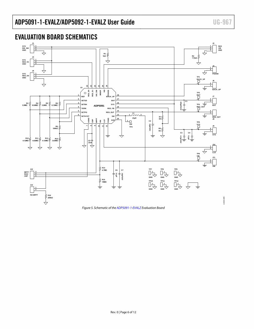
EVALUATION BOARD SCHEMATICS
J10
LLD
12
J6
BACK_UP
12
TP4SW
1
J13
FIX MPPT
12
R16200kΩ
J11
VIN
12
R144.7MΩ C6
0.1µF
C4
0.1µF
J9
SYS
12
J4
PGOOD
12
J8REG_OUT
12
TP3REG_OUT
1
TP8
GND
1TP9
GND
1
J2
VID123
C3
4.7µF/10V
U1
ADP5091
REF1
SETSD2
SETBK3
TERM4
SETPG5
SETHYST6
AG
ND
7
CB
P8
MPP
T9
VIN
10
LLD
11
PGN
D12
SW13
REG_OUT14
REG_FB15
SYS16
BAT17
BACK_UP18PG
GO
D19
VID
20M
INO
P21
DIS
_SW
22R
EG_D
123
REG
_D0
24
EXP25
J12
RDIV123
R133.83MΩ
R66.19MΩ
TP6VIN
1
R8100kΩ
TP2BAT
1
TP1BACK_UP
1
TP11
GND
1TP12
GND
1
TP7
GND
1
TP10
GND
1
TP5SYS
1
CBP
MPPT
RES
GND
C2
10µF/10V
L1
22µH
1 2
R9NC
R70Ω
R1518MΩ
C510nF
R11kΩ
SYS
J5
REG_D0123GND
R124.12MΩ
R55.9MΩ
SYS
R114.02MΩ
J3
REG_D1123GND
R46.04MΩ
R104.12MΩ
R35.9MΩ
SYS
J1
DIS_SW123GND
C7
10µF/10V
R2113kΩ
J7
BAT
12
C1220µF/6.3V
1444
3-00
5
Figure 5. Schematic of the ADP5091-1-EVALZ Evaluation Board
UG-967 ADP5091-1-EVALZ/ADP5092-1-EVALZ User Guide
Rev. 0 | Page 7 of 12
ADP5092
REF
SETSD
SETBK
TERM
SETPG
SETHYST
AG
ND
CB
P
MPP
T
VIN
REG
_GO
OD
PGN
D
SW
REG_OUT
REG_FB
SYS
BAT
BACK_UP
PGG
OD
VID
MIN
OP
DIS
_SW
REG
_D1
REG
_D0
EXP
J10
LLD
12
J6
BACK_UP
12
TP4SW
1
J13
FIX MPPT
12
R16200kΩ
J11
VIN
12
R144.7MΩ C6
0.1µF
C4
0.1µF
J9
SYS
12
J4
PGOOD
12
J8REG_OUT
12
TP3REG_OUT
1
TP8
GND
1TP9
GND
1
J2
VID123
C3
4.7µF/10V
U1
1
2
3
4
5
6
7 8 9 10 11 12
13
14
15
16
17
18
192021222324
25
J12
RDIV123
R133.83MΩ
R66.19MΩ
TP6VIN
1
R8100kΩ
TP2BAT
1
TP1BACK_UP
1
TP11
GND
1TP12
GND
1
TP7
GND
1
TP10
GND
1
TP5SYS
1
CBP
MPPT
RES
GND
C2
10µF/10V
L1
22µH
1 2
R9NC
R70Ω
R1518MΩ
C510nF
R11kΩ
SYS
J5
REG_D0123GND
R124.12MΩ
R55.9MΩ
SYS
R114.02MΩ
J3
REG_D1123GND
R46.04MΩ
R104.12MΩ
R35.9MΩ
SYS
J1
DIS_SW123GND
C7
10µF/10V
R2113kΩ
J7
BAT
12
C1220µF/6.3V
1444
3-00
6
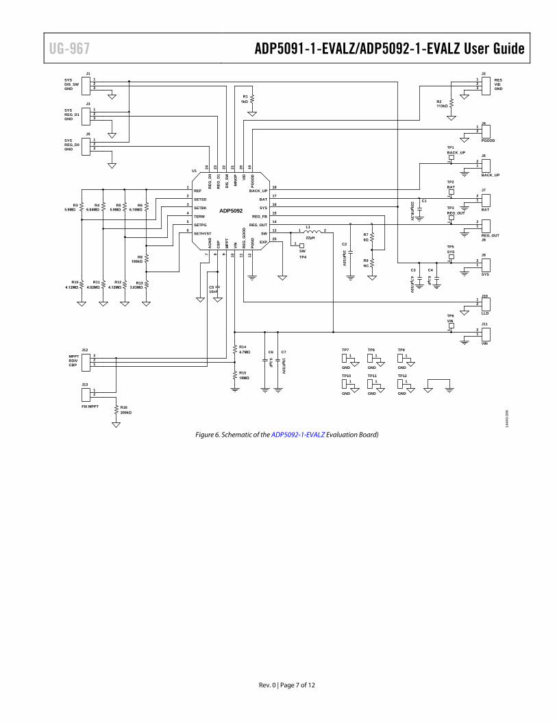
Figure 6. Schematic of the ADP5092-1-EVALZ Evaluation Board)
ADP5091-1-EVALZ/ADP5092-1-EVALZ User Guide UG-967
Rev. 0 | Page 8 of 12
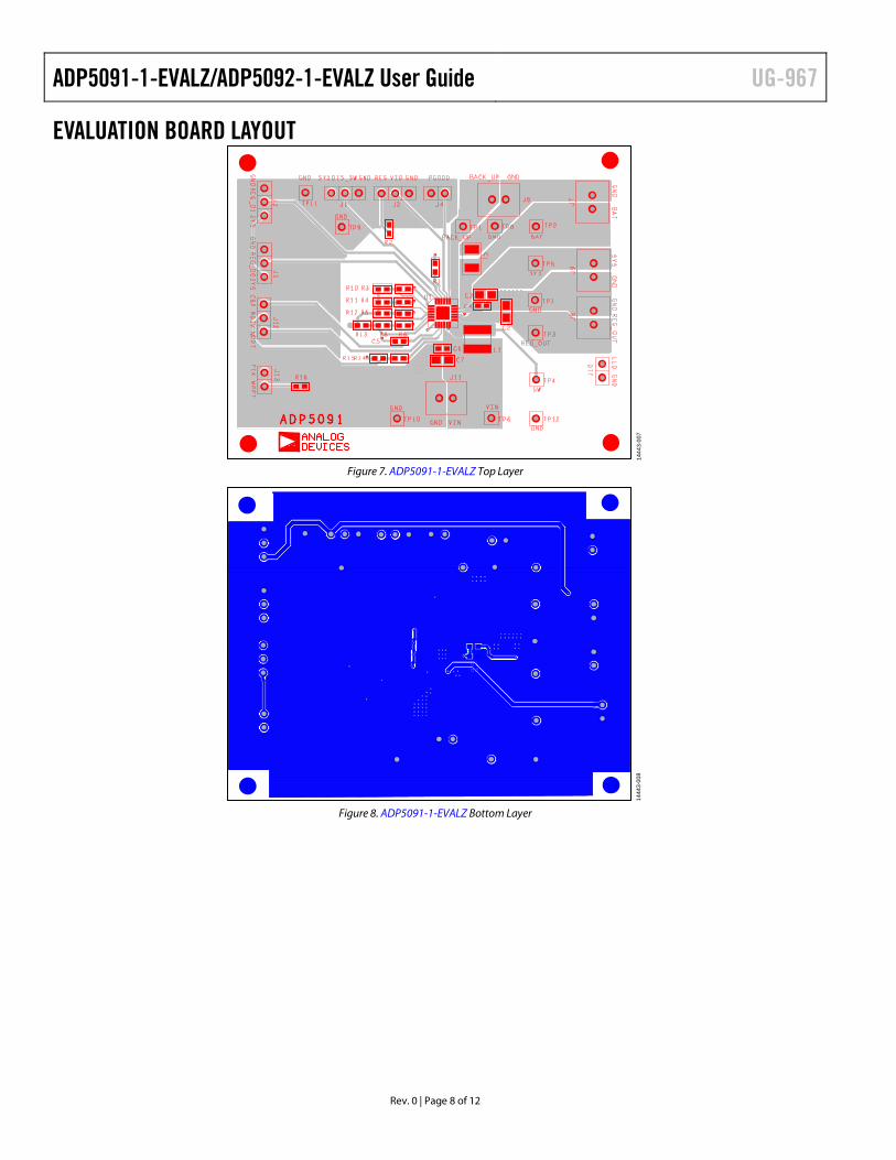
EVALUATION BOARD LAYOUT
1444
3-00
7
Figure 7. ADP5091-1-EVALZ Top Layer
1444
3-00
8
Figure 8. ADP5091-1-EVALZ Bottom Layer
UG-967 ADP5091-1-EVALZ/ADP5092-1-EVALZ User Guide
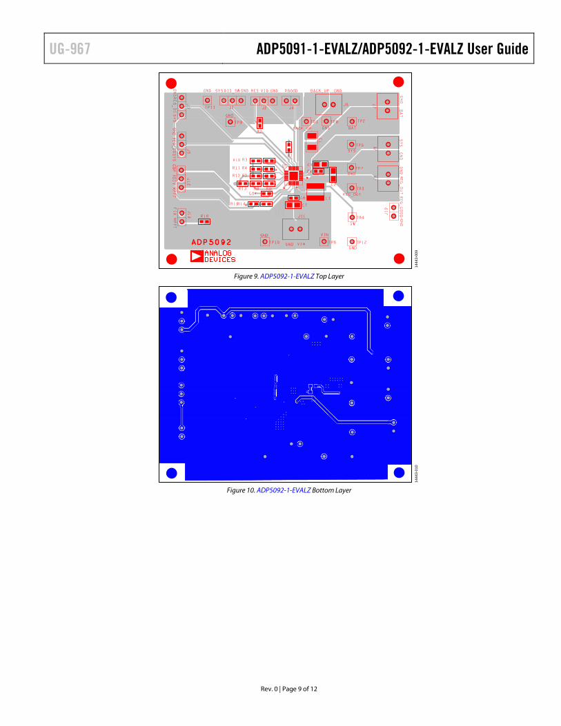
Rev. 0 | Page 9 of 12
1444
3-00
9
Figure 9. ADP5092-1-EVALZ Top Layer
1444
3-01
0
Figure 10. ADP5092-1-EVALZ Bottom Layer

ADP5091-1-EVALZ/ADP5092-1-EVALZ User Guide UG-967
Rev. 0 | Page 10 of 12
ORDERING INFORMATION BILL OF MATERIALS
Table 2. ADP5091-1-EVALZ Evaluation Board Bill of Materials Quantity Reference Designator Description Part Number PCB Footprint Vendor 1 C1 220 µF/6.3 V GRM32ER60J107ME20 C1210 Murata 2 C2, C7 10 µF/10 V GRM21BR71A106KE51 C0805 Murata 1 C3 4.7 µF/10 V GRM21BR61A475KA73 C0805 Murata 2 C4, C6 0.1 µF GRM188R71H104KA93 C0603 Murata 1 C5 10 nF GRM188R71H103KA01 C0603 Murata 1 J1 DIS_SW M20-9990246 SIP3 Harwin 1 J2 VID M20-9990246 SIP3 Harwin 1 J3 REG_D1 M20-9990246 SIP3 Harwin 1 J4 PGOOD M20-9990245 SIP2 Harwin 1 J5 REG_D0 M20-9990246 SIP3 Harwin 1 J6 BACK_UP 61900211121 SIP2 Würth 1 J7 BAT 61900211121? SIP2 Harwin 1 J8 REG_OUT 61900211121? SIP2 Harwin 1 J9 SYS 61900211121? SIP2 Harwin 1 J10 LLD M20-9990245 SIP2 Harwin 1 J11 VIN 61900211121? SIP Harwin 1 J12 RDIV M20-9990246 SIP3 Harwin 1 J13 FIX MPPT M20-9990245 SIP2 Harwin 1 L1 22 µH LPS4018-223MLB 4 mm × 4 mm Coilcraft 1 L1 22 µH 74437324220 4 mm × 4 mm Würth 1 R1 1 kΩ CRCW06031K00FKEA R0603 Vishay Dale 1 R2 113 kΩ CRCW0603113KFKEA R0603 Vishay Dale 2 R3, R5 5.9 MΩ CRCW06035M90FKEA R0603 Vishay Dale 1 R4 6.04 MΩ CRCW06036M04FKEA R0603 Vishay Dale 1 R6 6.19 MΩ CRCW06036M19FKEA R0603 Vishay Dale 1 R7 0 Ω CRCW06030000FKEA R0603 Vishay Dale 1 R8 100 kΩ CRCW0603100K0FKEA R0603 Vishay Dale 1 R9 NC N/A R0603 Vishay Dale 2 R10, R12 4.12 MΩ CRCW06034M12FKEA R0603 Vishay Dale 1 R11 4.02 MΩ CRCW06034M02FKEA R0603 Vishay Dale 1 R13 3.83 MΩ CRCW06033M83FKEA R0603 Vishay Dale 1 R14 4.7 MΩ CRCW06034M70FKEA R0603 Vishay Dale 1 R15 18 MΩ RK73B1JTTD186J R0603 KOA 1 R16 200 kΩ CRCW0603200KFKEA R0603 Vishay Dale 1 TP1 BACK_UP M20-9990245 SIP1 Harwin 1 TP2 BAT M20-9990245 SIP1 Harwin 1 TP3 REG_OUT M20-9990245 SIP1 Harwin 1 TP4 SW M20-9990245 SIP1 Harwin 1 TP5 SYS M20-9990245 SIP1 Harwin 1 TP6 VIN M20-9990245 SIP1 Harwin 6 TP7, TP8, TP9, TP10, TP11, TP12 GND M20-9990245 SIP1 Harwin 1 U1 ADP5091 ADP5091-ACZP-1-R7 24-lead LFCSP Analog Devices,
Inc.
UG-967 ADP5091-1-EVALZ/ADP5092-1-EVALZ User Guide
Rev. 0 | Page 11 of 12
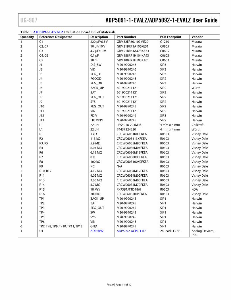
Table 3. ADP5092-1-EVALZ Evaluation Board Bill of Materials Quantity Reference Designator Description Part Number PCB Footprint Vendor 1 C1 220 µF/6.3 V GRM32ER60J107ME20 C1210 Murata 2 C2, C7 10 µF/10 V GRM21BR71A106KE51 C0805 Murata 1 C3 4.7 µF/10 V GRM21BR61A475KA73 C0805 Murata 2 C4, C6 0.1 µF GRM188R71H104KA93 C0603 Murata 1 C5 10 nF GRM188R71H103KA01 C0603 Murata 1 J1 DIS_SW M20-9990246 SIP3 Harwin 1 J2 VID M20-9990246 SIP3 Harwin 1 J3 REG_D1 M20-9990246 SIP3 Harwin 1 J4 PGOOD M20-9990245 SIP2 Harwin 1 J5 REG_D0 M20-9990246 SIP3 Harwin 1 J6 BACK_UP 601900211121 SIP2 Würth 1 J7 BAT 601900211121 SIP2 Harwin 1 J8 REG_OUT 601900211121 SIP2 Harwin 1 J9 SYS 601900211121 SIP2 Harwin 1 J10 REG_OUT M20-9990245 SIP2 Harwin 1 J11 VIN 601900211121 SIP2 Harwin 1 J12 RDIV M20-9990246 SIP3 Harwin 1 J13 FIX MPPT M20-9990245 SIP2 Harwin 1 L1 22 µH LPS4018-223MLB 4 mm × 4 mm Coilcraft 1 L1 22 µH 74437324220 4 mm × 4 mm Würth 1 R1 1 kΩ CRCW06031K00FKEA R0603 Vishay Dale 1 R2 113 kΩ CRCW0603113KFKEA R0603 Vishay Dale 2 R3, R5 5.9 MΩ CRCW06035M90FKEA R0603 Vishay Dale 1 R4 6.04 MΩ CRCW06036M04FKEA R0603 Vishay Dale 1 R6 6.19 MΩ CRCW06036M19FKEA R0603 Vishay Dale 1 R7 0 Ω CRCW06030000FKEA R0603 Vishay Dale 1 R8 100 kΩ CRCW0603100K0FKEA R0603 Vishay Dale 1 R9 NC N/A R0603 Vishay Dale 2 R10, R12 4.12 MΩ CRCW06034M12FKEA R0603 Vishay Dale 1 R11 4.02 MΩ CRCW06034M02FKEA R0603 Vishay Dale 1 R13 3.83 MΩ CRCW06033M83FKEA R0603 Vishay Dale 1 R14 4.7 MΩ CRCW06034M70FKEA R0603 Vishay Dale 1 R15 18 MΩ RK73B1JTTD186J R0603 KOA 1 R16 200 kΩ CRCW0603200KFKEA R0603 Vishay Dale 1 TP1 BACK_UP M20-9990245 SIP1 Harwin 1 TP2 BAT M20-9990245 SIP1 Harwin 1 TP3 REG_OUT M20-9990245 SIP1 Harwin 1 TP4 SW M20-9990245 SIP1 Harwin 1 TP5 SYS M20-9990245 SIP1 Harwin 1 TP6 VIN M20-9990245 SIP1 Harwin 6 TP7, TP8, TP9, TP10, TP11, TP12 GND M20-9990245 SIP1 Harwin 1 U1 ADP5092 ADP5092-ACPZ-1-R7 24-lead LFCSP Analog Devices,
Inc.
ADP5091-1-EVALZ/ADP5092-1-EVALZ User Guide UG-967
Rev. 0 | Page 12 of 12
NOTES
ESD Caution ESD (electrostatic discharge) sensitive device. Charged devices and circuit boards can discharge without detection. Although this product features patented or proprietary protection circuitry, damage may occur on devices subjected to high energy ESD. Therefore, proper ESD precautions should be taken to avoid performance degradation or loss of functionality.
Legal Terms and Conditions By using the evaluation board discussed herein (together with any tools, components documentation or support materials, the “Evaluation Board”), you are agreeing to be bound by the terms and conditions set forth below (“Agreement”) unless you have purchased the Evaluation Board, in which case the Analog Devices Standard Terms and Conditions of Sale shall govern. Do not use the Evaluation Board until you have read and agreed to the Agreement. Your use of the Evaluation Board shall signify your acceptance of the Agreement. This Agreement is made by and between you (“Customer”) and Analog Devices, Inc. (“ADI”), with its principal place of business at One Technology Way, Norwood, MA 02062, USA. Subject to the terms and conditions of the Agreement, ADI hereby grants to Customer a free, limited, personal, temporary, non-exclusive, non-sublicensable, non-transferable license to use the Evaluation Board FOR EVALUATION PURPOSES ONLY. Customer understands and agrees that the Evaluation Board is provided for the sole and exclusive purpose referenced above, and agrees not to use the Evaluation Board for any other purpose. Furthermore, the license granted is expressly made subject to the following additional limitations: Customer shall not (i) rent, lease, display, sell, transfer, assign, sublicense, or distribute the Evaluation Board; and (ii) permit any Third Party to access the Evaluation Board. As used herein, the term “Third Party” includes any entity other than ADI, Customer, their employees, affiliates and in-house consultants. The Evaluation Board is NOT sold to Customer; all rights not expressly granted herein, including ownership of the Evaluation Board, are reserved by ADI. CONFIDENTIALITY. This Agreement and the Evaluation Board shall all be considered the confidential and proprietary information of ADI. Customer may not disclose or transfer any portion of the Evaluation Board to any other party for any reason. Upon discontinuation of use of the Evaluation Board or termination of this Agreement, Customer agrees to promptly return the Evaluation Board to ADI. ADDITIONAL RESTRICTIONS. Customer may not disassemble, decompile or reverse engineer chips on the Evaluation Board. Customer shall inform ADI of any occurred damages or any modifications or alterations it makes to the Evaluation Board, including but not limited to soldering or any other activity that affects the material content of the Evaluation Board. Modifications to the Evaluation Board must comply with applicable law, including but not limited to the RoHS Directive. TERMINATION. ADI may terminate this Agreement at any time upon giving written notice to Customer. Customer agrees to return to ADI the Evaluation Board at that time. LIMITATION OF LIABILITY. THE EVALUATION BOARD PROVIDED HEREUNDER IS PROVIDED “AS IS” AND ADI MAKES NO WARRANTIES OR REPRESENTATIONS OF ANY KIND WITH RESPECT TO IT. ADI SPECIFICALLY DISCLAIMS ANY REPRESENTATIONS, ENDORSEMENTS, GUARANTEES, OR WARRANTIES, EXPRESS OR IMPLIED, RELATED TO THE EVALUATION BOARD INCLUDING, BUT NOT LIMITED TO, THE IMPLIED WARRANTY OF MERCHANTABILITY, TITLE, FITNESS FOR A PARTICULAR PURPOSE OR NONINFRINGEMENT OF INTELLECTUAL PROPERTY RIGHTS. IN NO EVENT WILL ADI AND ITS LICENSORS BE LIABLE FOR ANY INCIDENTAL, SPECIAL, INDIRECT, OR CONSEQUENTIAL DAMAGES RESULTING FROM CUSTOMER’S POSSESSION OR USE OF THE EVALUATION BOARD, INCLUDING BUT NOT LIMITED TO LOST PROFITS, DELAY COSTS, LABOR COSTS OR LOSS OF GOODWILL. ADI’S TOTAL LIABILITY FROM ANY AND ALL CAUSES SHALL BE LIMITED TO THE AMOUNT OF ONE HUNDRED US DOLLARS ($100.00). EXPORT. Customer agrees that it will not directly or indirectly export the Evaluation Board to another country, and that it will comply with all applicable United States federal laws and regulations relating to exports. GOVERNING LAW. This Agreement shall be governed by and construed in accordance with the substantive laws of the Commonwealth of Massachusetts (excluding conflict of law rules). Any legal action regarding this Agreement will be heard in the state or federal courts having jurisdiction in Suffolk County, Massachusetts, and Customer hereby submits to the personal jurisdiction and venue of such courts. The United Nations Convention on Contracts for the International Sale of Goods shall not apply to this Agreement and is expressly disclaimed.
©2016 Analog Devices, Inc. All rights reserved. Trademarks and registered trademarks are the property of their respective owners. UG14443-0-5/16(0)