Embed Size (px)
Citation preview
REFQ,typ
REF
VI
R=
1
2
3
4
8
7
6
5
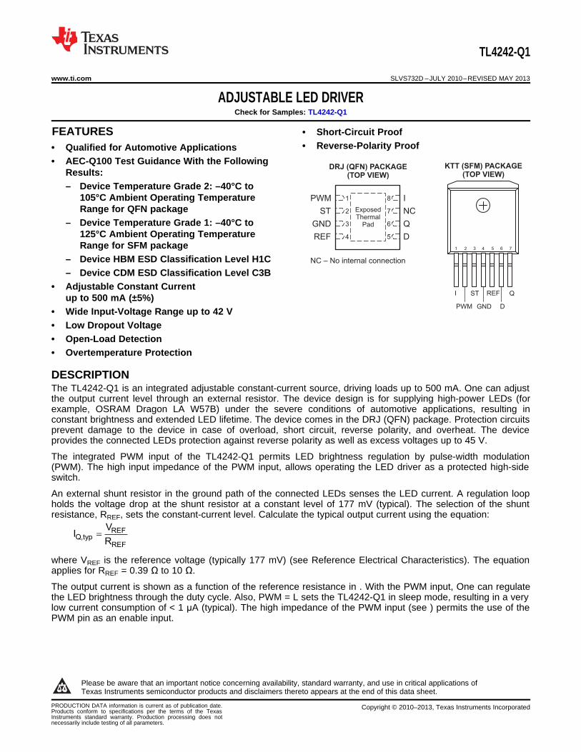
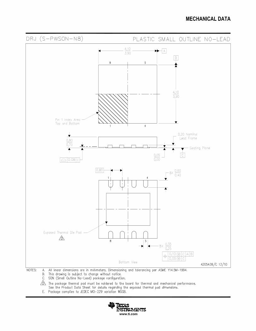
DRJ (QFN) PACKAGE(TOP VIEW)
I
NC
Q
D
PWM
ST
GND
REF
NC – No internal connection
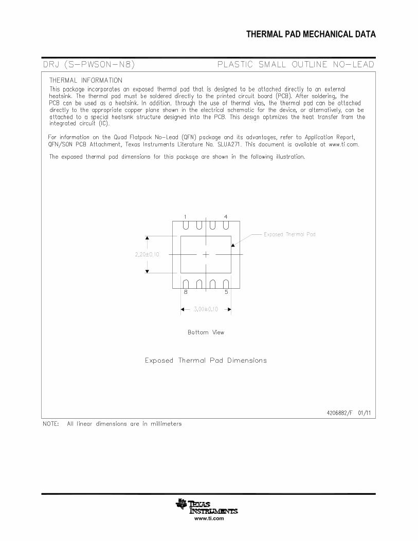
ExposedThermal
Pad
1 2 3 4 765
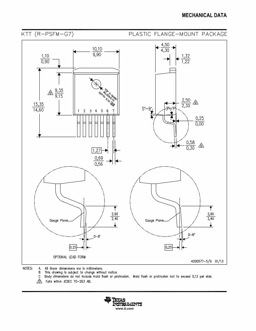
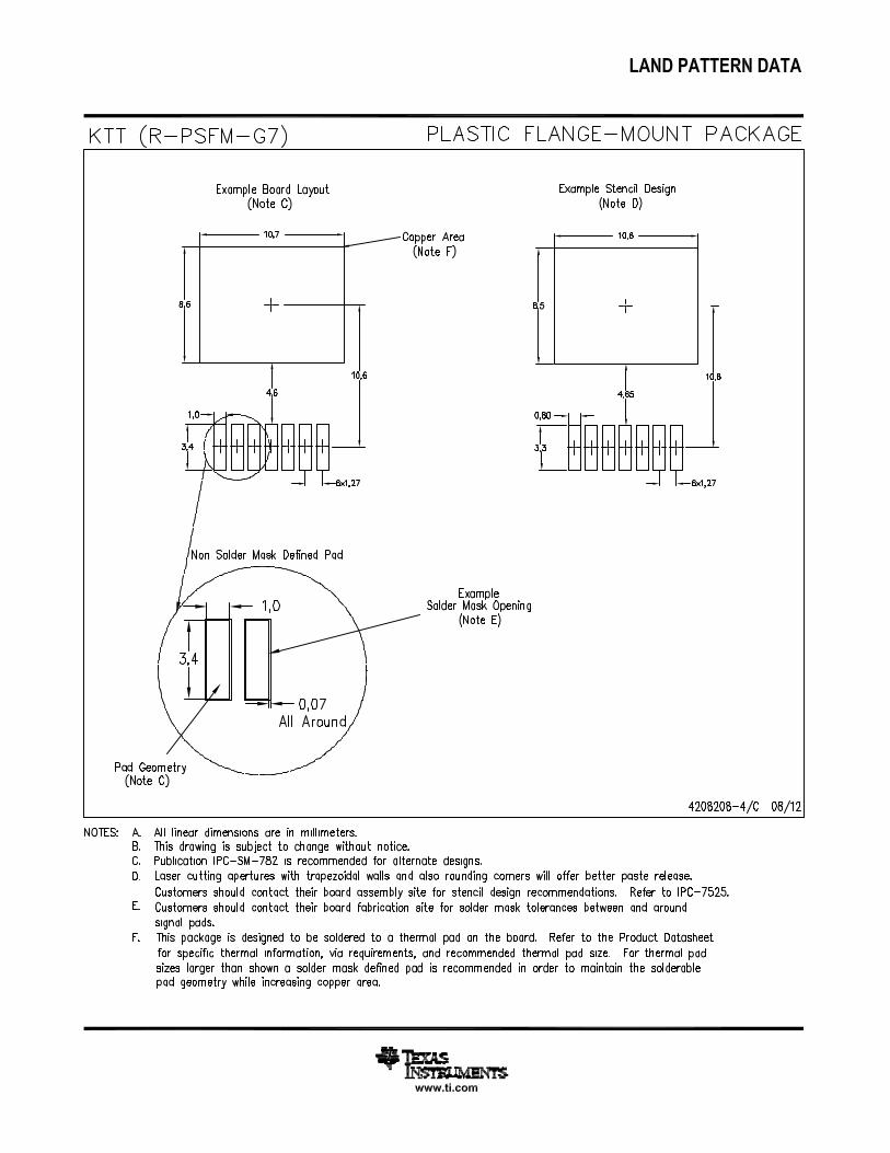
KTT (SFM) PACKAGE(TOP VIEW)
I Q
DPWM
ST
GND
REF
TL4242-Q1
www.ti.com SLVS732D –JULY 2010–REVISED MAY 2013
ADJUSTABLE LED DRIVERCheck for Samples: TL4242-Q1
1FEATURES • Short-Circuit Proof• Reverse-Polarity Proof• Qualified for Automotive Applications
• AEC-Q100 Test Guidance With the FollowingResults:– Device Temperature Grade 2: –40°C to
105°C Ambient Operating TemperatureRange for QFN package
– Device Temperature Grade 1: –40°C to125°C Ambient Operating TemperatureRange for SFM package
– Device HBM ESD Classification Level H1C– Device CDM ESD Classification Level C3B
• Adjustable Constant Currentup to 500 mA (±5%)
• Wide Input-Voltage Range up to 42 V• Low Dropout Voltage• Open-Load Detection• Overtemperature Protection
DESCRIPTIONThe TL4242-Q1 is an integrated adjustable constant-current source, driving loads up to 500 mA. One can adjustthe output current level through an external resistor. The device design is for supplying high-power LEDs (forexample, OSRAM Dragon LA W57B) under the severe conditions of automotive applications, resulting inconstant brightness and extended LED lifetime. The device comes in the DRJ (QFN) package. Protection circuitsprevent damage to the device in case of overload, short circuit, reverse polarity, and overheat. The deviceprovides the connected LEDs protection against reverse polarity as well as excess voltages up to 45 V.
The integrated PWM input of the TL4242-Q1 permits LED brightness regulation by pulse-width modulation(PWM). The high input impedance of the PWM input, allows operating the LED driver as a protected high-sideswitch.
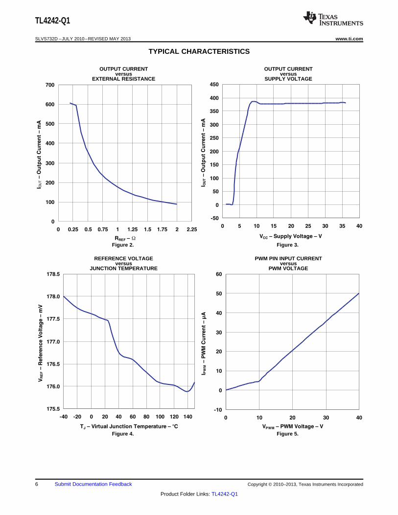
An external shunt resistor in the ground path of the connected LEDs senses the LED current. A regulation loopholds the voltage drop at the shunt resistor at a constant level of 177 mV (typical). The selection of the shuntresistance, RREF, sets the constant-current level. Calculate the typical output current using the equation:
where VREF is the reference voltage (typically 177 mV) (see Reference Electrical Characteristics). The equationapplies for RREF = 0.39 Ω to 10 Ω.
The output current is shown as a function of the reference resistance in . With the PWM input, One can regulatethe LED brightness through the duty cycle. Also, PWM = L sets the TL4242-Q1 in sleep mode, resulting in a verylow current consumption of < 1 μA (typical). The high impedance of the PWM input (see ) permits the use of thePWM pin as an enable input.
1
Please be aware that an important notice concerning availability, standard warranty, and use in critical applications ofTexas Instruments semiconductor products and disclaimers thereto appears at the end of this data sheet.
PRODUCTION DATA information is current as of publication date. Copyright © 2010–2013, Texas Instruments IncorporatedProducts conform to specifications per the terms of the TexasInstruments standard warranty. Production processing does notnecessarily include testing of all parameters.
QI
GND
PWM
ST
REF
D
Bias Supply
BandgapReference
Comparator
+
−
StatusDelay
8
4
5
6
3
2
1
TL4242-Q1
SLVS732D –JULY 2010–REVISED MAY 2013 www.ti.com
This integrated circuit can be damaged by ESD. Texas Instruments recommends that all integrated circuits be handled withappropriate precautions. Failure to observe proper handling and installation procedures can cause damage.
ESD damage can range from subtle performance degradation to complete device failure. Precision integrated circuits may be moresusceptible to damage because very small parametric changes could cause the device not to meet its published specifications.
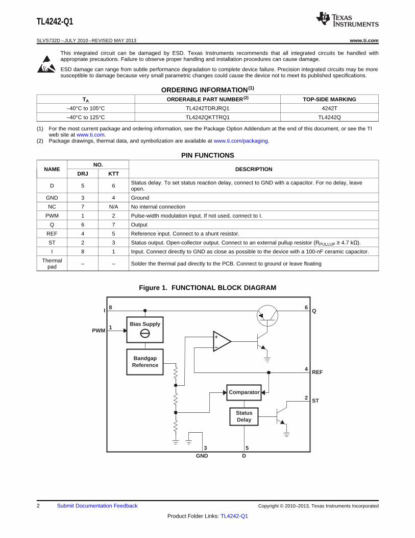
ORDERING INFORMATION (1)
TA ORDERABLE PART NUMBER (2) TOP-SIDE MARKING
–40°C to 105°C TL4242TDRJRQ1 4242T
–40°C to 125°C TL4242QKTTRQ1 TL4242Q
(1) For the most current package and ordering information, see the Package Option Addendum at the end of this document, or see the TIweb site at www.ti.com.
(2) Package drawings, thermal data, and symbolization are available at www.ti.com/packaging.
PIN FUNCTIONSNO.
NAME DESCRIPTIONDRJ KTT
Status delay. To set status reaction delay, connect to GND with a capacitor. For no delay, leaveD 5 6 open.
GND 3 4 Ground
NC 7 N/A No internal connection
PWM 1 2 Pulse-width modulation input. If not used, connect to I.
Q 6 7 Output
REF 4 5 Reference input. Connect to a shunt resistor.
ST 2 3 Status output. Open-collector output. Connect to an external pullup resistor (RPULLUP ≥ 4.7 kΩ).
I 8 1 Input. Connect directly to GND as close as possible to the device with a 100-nF ceramic capacitor.
Thermal – – Solder the thermal pad directly to the PCB. Connect to ground or leave floatingpad
Figure 1. FUNCTIONAL BLOCK DIAGRAM
2 Submit Documentation Feedback Copyright © 2010–2013, Texas Instruments Incorporated
Product Folder Links: TL4242-Q1
TL4242-Q1
www.ti.com SLVS732D –JULY 2010–REVISED MAY 2013
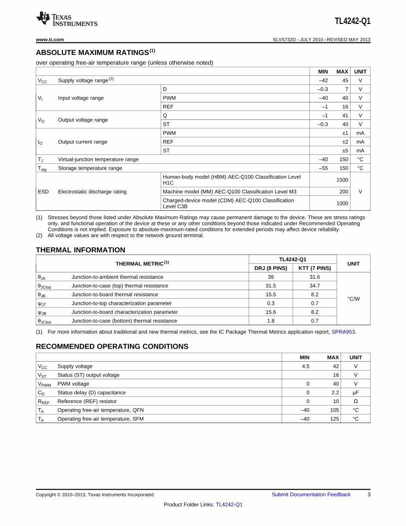
ABSOLUTE MAXIMUM RATINGS (1)
over operating free-air temperature range (unless otherwise noted)
MIN MAX UNIT
VCC Supply voltage range (2) –42 45 V
D –0.3 7 V
VI Input voltage range PWM –40 40 V
REF –1 16 V
Q –1 41 VVO Output voltage range
ST –0.3 40 V
PWM ±1 mA
IO Output current range REF ±2 mA
ST ±5 mA
TJ Virtual-junction temperature range –40 150 °C
Tstg Storage temperature range –55 150 °C
Human-body model (HBM) AEC-Q100 Classification Level 1500H1C
ESD Electrostatic discharge rating Machine model (MM) AEC-Q100 Classification Level M3 200 V
Charged-device model (CDM) AEC-Q100 Classification 1000Level C3B
(1) Stresses beyond those listed under Absolute Maximum Ratings may cause permanent damage to the device. These are stress ratingsonly, and functional operation of the device at these or any other conditions beyond those indicated under Recommended OperatingConditions is not implied. Exposure to absolute-maximum-rated conditions for extended periods may affect device reliability.
(2) All voltage values are with respect to the network ground terminal.
THERMAL INFORMATIONTL4242-Q1
THERMAL METRIC (1) UNITDRJ (8 PINS) KTT (7 PINS)
θJA Junction-to-ambient thermal resistance 39 31.6
θJCtop Junction-to-case (top) thermal resistance 31.5 34.7
θJB Junction-to-board thermal resistance 15.5 8.2°C/W
ψJT Junction-to-top characterization parameter 0.3 0.7
ψJB Junction-to-board characterization parameter 15.6 8.2
θJCbot Junction-to-case (bottom) thermal resistance 1.8 0.7
(1) For more information about traditional and new thermal metrics, see the IC Package Thermal Metrics application report, SPRA953.
RECOMMENDED OPERATING CONDITIONSMIN MAX UNIT
VCC Supply voltage 4.5 42 V
VST Status (ST) output voltage 16 V
VPWM PWM voltage 0 40 V
CD Status delay (D) capacitance 0 2.2 μF
RREF Reference (REF) resistor 0 10 ΩTA Operating free-air temperature, QFN –40 105 °C
TA Operating free-air temperature, SFM –40 125 °C
Copyright © 2010–2013, Texas Instruments Incorporated Submit Documentation Feedback 3
Product Folder Links: TL4242-Q1
TL4242-Q1
SLVS732D –JULY 2010–REVISED MAY 2013 www.ti.com
OVERALL DEVICE ELECTRICAL CHARACTERISTICSover recommended operating free-air temperature range, VI = 13.5 V, RREF = 0.47 Ω, VPWM,H, TA = –40°C to 105°C (QFN),TA = –40°C to 125°C (SFM), all voltages with respect to ground (unless otherwise noted)
PARAMETER TEST CONDITIONS MIN TYP MAX UNIT
IqL Supply current VQ = 6.6 V 12 22 mA
IqOFF Supply current, off mode PWM = L, TJ < 85°C 0.1 2 μA
OUTPUT ELECTRICAL CHARACTERISTICSover recommended operating free-air temperature range, VI = 13.5 V, RREF = 0.47 Ω, VPWM,H, TA = –40°C to 105°C (QFN),TA = –40°C to 125°C (SFM), all voltages with respect to ground (unless otherwise noted)
PARAMETER TEST CONDITIONS MIN TYP MAX UNIT
VQ – VREF(1) = 6.6 V 357 376 395
VQ – VREF = 6.6 V, RREF = 1 Ω 168 177 185IQ Output current mA
VQ – VREF = 6.6 V, RREF = 0.39 Ω 431 454 476
VQ – VREF = 5.4 V to 7.8 V, VI = 9 V to 16 V 357 376 395
IQmax Output current limit RREF = 0 Ω 600 mA
Vdr Drop voltage IQ = 300 mA 0.35 0.7 V
(1) VQ – VREF equals the forward voltage sum of the connected LEDs (see ).
PWM INPUT ELECTRICAL CHARACTERISTICSover recommended operating free-air temperature range, VI = 13.5 V, RREF = 0.47 Ω, VPWM,H, TA = –40°C to 105°C (QFN),TA = -40°C to 125°C (SFM), all voltages with respect to ground (unless otherwise noted)
PARAMETER TEST CONDITIONS MIN TYP MAX UNIT
VPWM,H High-level PWM voltage 2.6 V
VPWM,L Low-level PWM voltage 0.7 V
IPWM,H High-level PWM input current VPWM = 5 V 220 500 μA
IPWM,L Low-level PWM input current VPWM = 0 V –1 1 μA
tPWM,ON Delay time, turnon 70% of IQnom, see Figure 7 0 15 40 μs
tPWM,OFF Delay time, turnoff 30% of IQnom, see Figure 7 0 15 40 μs
REFERENCE (REF) ELECTRICAL CHARACTERISTICSover recommended operating free-air temperature range, VI = 13.5 V, RREF = 0.47 Ω, VPWM,H, TA = –40°C to 105°C (QFN),TA = –40°C to 125°C (SFM), all voltages with respect to ground (unless otherwise noted)
PARAMETER TEST CONDITIONS MIN TYP MAX UNIT
VREF Reference voltage RREF = 0.39 Ω to 1 Ω 168 177 185 mV
IREF Reference input current VREF = 180 mV –1 0.1 1 μA
4 Submit Documentation Feedback Copyright © 2010–2013, Texas Instruments Incorporated
Product Folder Links: TL4242-Q1
TL4242-Q1
www.ti.com SLVS732D –JULY 2010–REVISED MAY 2013
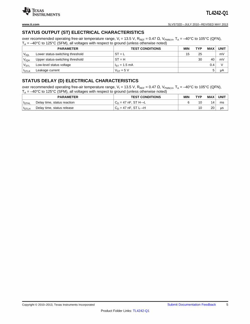
STATUS OUTPUT (ST) ELECTRICAL CHARACTERISTICSover recommended operating free-air temperature range, VI = 13.5 V, RREF = 0.47 Ω, VPWM,H, TA = –40°C to 105°C (QFN),TA = –40°C to 125°C (SFM), all voltages with respect to ground (unless otherwise noted)
PARAMETER TEST CONDITIONS MIN TYP MAX UNIT
VIQL Lower status-switching threshold ST = L 15 25 mV
VIQH Upper status-switching threshold ST = H 30 40 mV
VSTL Low-level status voltage IST = 1.5 mA 0.4 V
ISTLK Leakage current VST = 5 V 5 μA
STATUS DELAY (D) ELECTRICAL CHARACTERISTICSover recommended operating free-air temperature range, VI = 13.5 V, RREF = 0.47 Ω, VPWM,H, TA = –40°C to 105°C (QFN),TA = –40°C to 125°C (SFM), all voltages with respect to ground (unless otherwise noted)
PARAMETER TEST CONDITIONS MIN TYP MAX UNIT
tSTHL Delay time, status reaction CD = 47 nF, ST H→L 6 10 14 ms
tSTLH Delay time, status release CD = 47 nF, ST L→H 10 20 μs
Copyright © 2010–2013, Texas Instruments Incorporated Submit Documentation Feedback 5
Product Folder Links: TL4242-Q1
175.5
176.0
176.5
177.0
177.5
178.0
178.5
-40 -20 0 20 40 60 80 100 120 140
TJ – Virtual Junction Temperature – °C
VR
EF
–R
efe
ren
ce
Vo
ltag
e–
mV
-10
0
10
20
30
40
50
60
0 10 20 30 40
VPWM – PWM Voltage – V
I PW
M–
PW
MC
urr
en
t–
µA
0
100
200
300
400
500
600
700
0 0.25 0.5 0.75 1 1.25 1.5 1.75 2 2.25
RREF – 8
I OU
T–
Ou
tpu
tC
urr
en
t–
mA
W
-50
0
50
100
150
200
250
300
350
400
450
0 5 10 15 20 25 30 35 40
VCC – Supply Voltage – V
I OU
T–
Ou
tpu
tC
urr
en
t–
mA
TL4242-Q1
SLVS732D –JULY 2010–REVISED MAY 2013 www.ti.com
TYPICAL CHARACTERISTICS
OUTPUT CURRENT OUTPUT CURRENTversus versus
EXTERNAL RESISTANCE SUPPLY VOLTAGE
Figure 2. Figure 3.
REFERENCE VOLTAGE PWM PIN INPUT CURRENTversus versus
JUNCTION TEMPERATURE PWM VOLTAGE
Figure 4. Figure 5.
6 Submit Documentation Feedback Copyright © 2010–2013, Texas Instruments Incorporated
Product Folder Links: TL4242-Q1
tSTLH,typCD
47 nF 10 s
tSTHL,typCD
47 nF 10 ms
100 nF
Q
SI
ROI
GNDRADJ D 10 µF 10 kW
ST PWM
GND D
47 nF
Q
REF
VBAT
RREF
LED
Dragon
I
Microcontroller
0.47 W
0.25 W
TL4242-Q1
TL4242-Q1
www.ti.com SLVS732D –JULY 2010–REVISED MAY 2013
APPLICATION INFORMATION
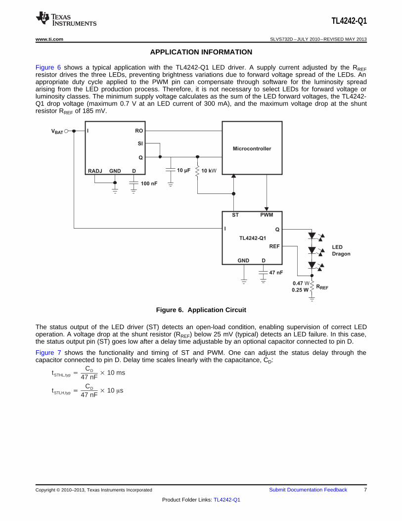
Figure 6 shows a typical application with the TL4242-Q1 LED driver. A supply current adjusted by the RREFresistor drives the three LEDs, preventing brightness variations due to forward voltage spread of the LEDs. Anappropriate duty cycle applied to the PWM pin can compensate through software for the luminosity spreadarising from the LED production process. Therefore, it is not necessary to select LEDs for forward voltage orluminosity classes. The minimum supply voltage calculates as the sum of the LED forward voltages, the TL4242-Q1 drop voltage (maximum 0.7 V at an LED current of 300 mA), and the maximum voltage drop at the shuntresistor RREF of 185 mV.
Figure 6. Application Circuit
The status output of the LED driver (ST) detects an open-load condition, enabling supervision of correct LEDoperation. A voltage drop at the shunt resistor (RREF) below 25 mV (typical) detects an LED failure. In this case,the status output pin (ST) goes low after a delay time adjustable by an optional capacitor connected to pin D.
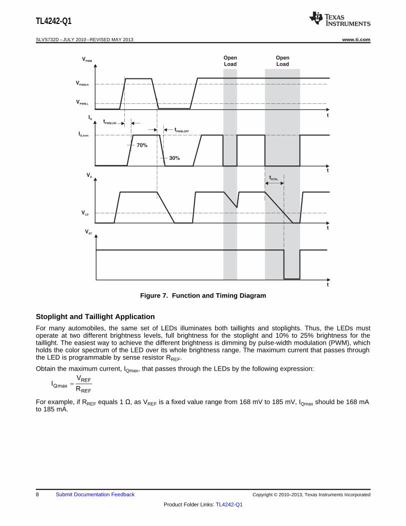
Figure 7 shows the functionality and timing of ST and PWM. One can adjust the status delay through thecapacitor connected to pin D. Delay time scales linearly with the capacitance, CD:
Copyright © 2010–2013, Texas Instruments Incorporated Submit Documentation Feedback 7
Product Folder Links: TL4242-Q1
REF
Qmax
REF
VI
R=
tPWM,OFF
30%
70%
tPWM,ON
tSTHL
Open
Load
Open
Load
t
t
t
t
VPWM
VPWM,H
VPWM,L
IQ,nom
IQ
VLD
VD
VST
TL4242-Q1
SLVS732D –JULY 2010–REVISED MAY 2013 www.ti.com
Figure 7. Function and Timing Diagram
Stoplight and Taillight Application
For many automobiles, the same set of LEDs illuminates both taillights and stoplights. Thus, the LEDs mustoperate at two different brightness levels, full brightness for the stoplight and 10% to 25% brightness for thetaillight. The easiest way to achieve the different brightness is dimming by pulse-width modulation (PWM), whichholds the color spectrum of the LED over its whole brightness range. The maximum current that passes throughthe LED is programmable by sense resistor RREF.
Obtain the maximum current, IQmax, that passes through the LEDs by the following expression:
For example, if RREF equals 1 Ω, as VREF is a fixed value range from 168 mV to 185 mV, IQmax should be 168 mAto 185 mA.
8 Submit Documentation Feedback Copyright © 2010–2013, Texas Instruments Incorporated
Product Folder Links: TL4242-Q1
J A JAT T P= + q ´
I O O I QP (V V ) I V I= - ´ + ´
TL4242-Q1
PWM
Q
REF
Vin
VDD OUT
TLC555-Q1
STOP
TAILRREF
LEDDragon
TL4242-Q1
www.ti.com SLVS732D –JULY 2010–REVISED MAY 2013
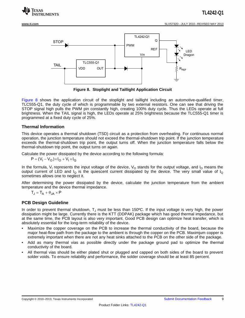
Figure 8. Stoplight and Taillight Application Circuit
Figure 8 shows the application circuit of the stoplight and taillight including an automotive-qualified timer,TLC555-Q1, the duty cycle of which is programmable by two external resistors. One can see that driving theSTOP signal high pulls the PWM pin constantly high, creating 100% duty cycle. Thus the LEDs operate at fullbrightness. When the TAIL signal is high, the LEDs operate at 25% brightness because the TLC555-Q1 timer isprogrammed at a fixed duty cycle of 25%.
Thermal Information
This device operates a thermal shutdown (TSD) circuit as a protection from overheating. For continuous normaloperation, the junction temperature should not exceed the thermal-shutdown trip point. If the junction temperatureexceeds the thermal-shutdown trip point, the output turns off. When the junction temperature falls below thethermal-shutdown trip point, the output turns on again.
Calculate the power dissipated by the device according to the following formula:
In the formula, VI represents the input voltage of the device, VO stands for the output voltage, and IO means theoutput current of LED and IQ is the quiescent current dissipated by the device. The very small value of IQsometimes allows one to neglect it.
After determining the power dissipated by the device, calculate the junction temperature from the ambienttemperature and the device thermal impedance.
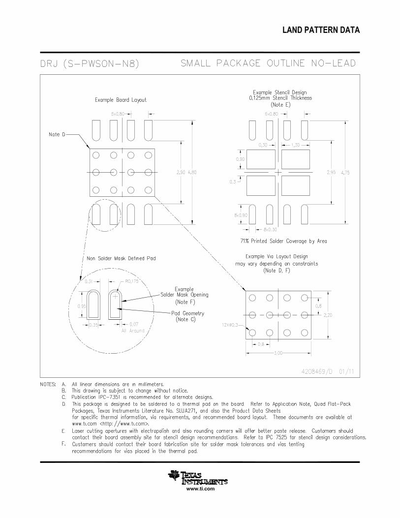
PCB Design Guideline
In order to prevent thermal shutdown, TJ must be less than 150ºC. If the input voltage is very high, the powerdissipation might be large. Currently there is the KTT (DDPAK) package which has good thermal impedance, butat the same time, the PCB layout is also very important. Good PCB design can optimize heat transfer, which isabsolutely essential for the long-term reliability of the device.• Maximize the copper coverage on the PCB to increase the thermal conductivity of the board, because the
major heat-flow path from the package to the ambient is through the copper on the PCB. Maximjum copper isextremely important when there are not any heat sinks attached to the PCB on the other side of the package.
• Add as many thermal vias as possible directly under the package ground pad to optimize the thermalconductivity of the board.
• All thermal vias should be either plated shut or plugged and capped on both sides of the board to preventsolder voids. To ensure reliability and performance, the solder coverage should be at least 85 percent.
Copyright © 2010–2013, Texas Instruments Incorporated Submit Documentation Feedback 9
Product Folder Links: TL4242-Q1
TL4242-Q1
SLVS732D –JULY 2010–REVISED MAY 2013 www.ti.com
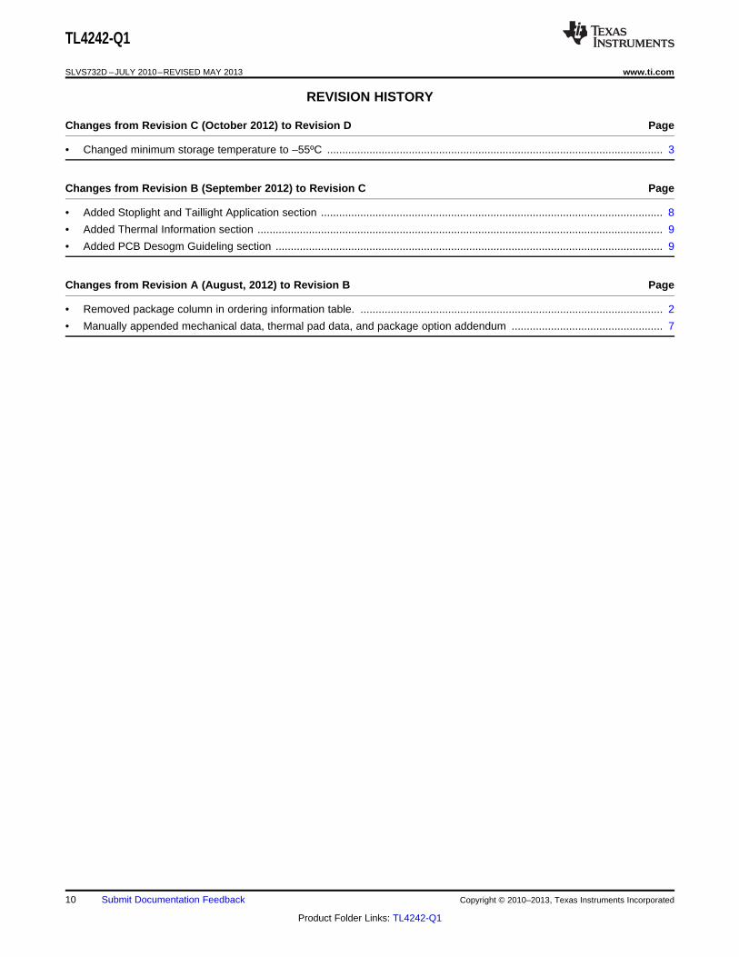
REVISION HISTORY
Changes from Revision C (October 2012) to Revision D Page
• Changed minimum storage temperature to –55ºC ............................................................................................................... 3
Changes from Revision B (September 2012) to Revision C Page
• Added Stoplight and Taillight Application section ................................................................................................................. 8
• Added Thermal Information section ...................................................................................................................................... 9
• Added PCB Desogm Guideling section ................................................................................................................................ 9
Changes from Revision A (August, 2012) to Revision B Page
• Removed package column in ordering information table. .................................................................................................... 2
• Manually appended mechanical data, thermal pad data, and package option addendum .................................................. 7
10 Submit Documentation Feedback Copyright © 2010–2013, Texas Instruments Incorporated
Product Folder Links: TL4242-Q1
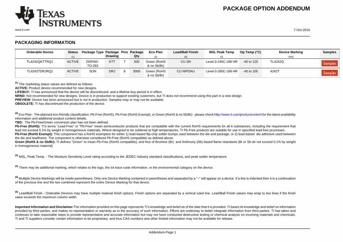
PACKAGE OPTION ADDENDUM
www.ti.com 7-Oct-2016
Addendum-Page 1
PACKAGING INFORMATION
Orderable Device Status(1)
Package Type PackageDrawing
Pins PackageQty
Eco Plan(2)
Lead/Ball Finish(6)
MSL Peak Temp(3)
Op Temp (°C) Device Marking(4/5)
Samples
TL4242QKTTRQ1 ACTIVE DDPAK/TO-263
KTT 7 500 Green (RoHS& no Sb/Br)
CU SN Level-3-245C-168 HR -40 to 125 TL4242Q
TL4242TDRJRQ1 ACTIVE SON DRJ 8 3000 Green (RoHS& no Sb/Br)
CU NIPDAU Level-3-260C-168 HR -40 to 105 4242T
(1) The marketing status values are defined as follows:ACTIVE: Product device recommended for new designs.LIFEBUY: TI has announced that the device will be discontinued, and a lifetime-buy period is in effect.NRND: Not recommended for new designs. Device is in production to support existing customers, but TI does not recommend using this part in a new design.PREVIEW: Device has been announced but is not in production. Samples may or may not be available.OBSOLETE: TI has discontinued the production of the device.
(2) Eco Plan - The planned eco-friendly classification: Pb-Free (RoHS), Pb-Free (RoHS Exempt), or Green (RoHS & no Sb/Br) - please check http://www.ti.com/productcontent for the latest availabilityinformation and additional product content details.TBD: The Pb-Free/Green conversion plan has not been defined.Pb-Free (RoHS): TI's terms "Lead-Free" or "Pb-Free" mean semiconductor products that are compatible with the current RoHS requirements for all 6 substances, including the requirement thatlead not exceed 0.1% by weight in homogeneous materials. Where designed to be soldered at high temperatures, TI Pb-Free products are suitable for use in specified lead-free processes.Pb-Free (RoHS Exempt): This component has a RoHS exemption for either 1) lead-based flip-chip solder bumps used between the die and package, or 2) lead-based die adhesive used betweenthe die and leadframe. The component is otherwise considered Pb-Free (RoHS compatible) as defined above.Green (RoHS & no Sb/Br): TI defines "Green" to mean Pb-Free (RoHS compatible), and free of Bromine (Br) and Antimony (Sb) based flame retardants (Br or Sb do not exceed 0.1% by weightin homogeneous material)
(3) MSL, Peak Temp. - The Moisture Sensitivity Level rating according to the JEDEC industry standard classifications, and peak solder temperature.
(4) There may be additional marking, which relates to the logo, the lot trace code information, or the environmental category on the device.
(5) Multiple Device Markings will be inside parentheses. Only one Device Marking contained in parentheses and separated by a "~" will appear on a device. If a line is indented then it is a continuationof the previous line and the two combined represent the entire Device Marking for that device.
(6) Lead/Ball Finish - Orderable Devices may have multiple material finish options. Finish options are separated by a vertical ruled line. Lead/Ball Finish values may wrap to two lines if the finishvalue exceeds the maximum column width.
Important Information and Disclaimer:The information provided on this page represents TI's knowledge and belief as of the date that it is provided. TI bases its knowledge and belief on informationprovided by third parties, and makes no representation or warranty as to the accuracy of such information. Efforts are underway to better integrate information from third parties. TI has taken andcontinues to take reasonable steps to provide representative and accurate information but may not have conducted destructive testing or chemical analysis on incoming materials and chemicals.TI and TI suppliers consider certain information to be proprietary, and thus CAS numbers and other limited information may not be available for release.
PACKAGE OPTION ADDENDUM
www.ti.com 7-Oct-2016
Addendum-Page 2
In no event shall TI's liability arising out of such information exceed the total purchase price of the TI part(s) at issue in this document sold by TI to Customer on an annual basis.
OTHER QUALIFIED VERSIONS OF TL4242-Q1 :
• Catalog: TL4242
NOTE: Qualified Version Definitions:
• Catalog - TI's standard catalog product
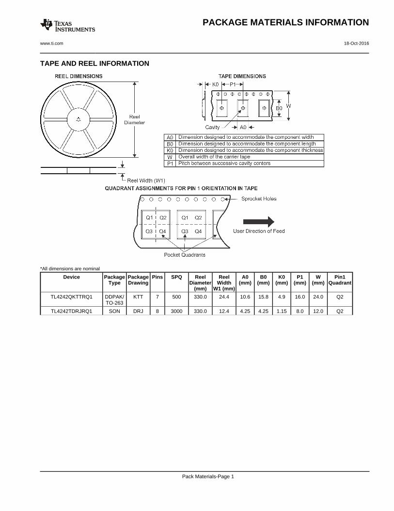
TAPE AND REEL INFORMATION
*All dimensions are nominal
Device PackageType
PackageDrawing
Pins SPQ ReelDiameter
(mm)
ReelWidth
W1 (mm)
A0(mm)
B0(mm)
K0(mm)
P1(mm)
W(mm)
Pin1Quadrant
TL4242QKTTRQ1 DDPAK/TO-263
KTT 7 500 330.0 24.4 10.6 15.8 4.9 16.0 24.0 Q2
TL4242TDRJRQ1 SON DRJ 8 3000 330.0 12.4 4.25 4.25 1.15 8.0 12.0 Q2
PACKAGE MATERIALS INFORMATION
www.ti.com 18-Oct-2016
Pack Materials-Page 1
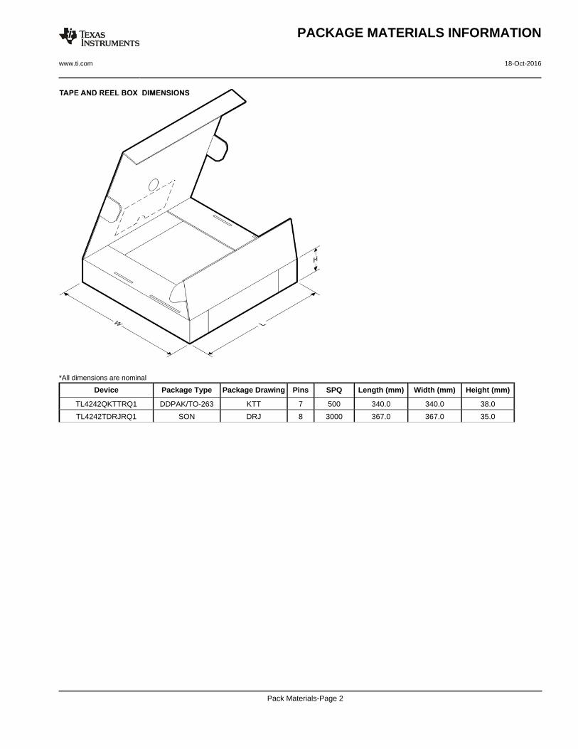
*All dimensions are nominal
Device Package Type Package Drawing Pins SPQ Length (mm) Width (mm) Height (mm)
TL4242QKTTRQ1 DDPAK/TO-263 KTT 7 500 340.0 340.0 38.0
TL4242TDRJRQ1 SON DRJ 8 3000 367.0 367.0 35.0
PACKAGE MATERIALS INFORMATION
www.ti.com 18-Oct-2016
Pack Materials-Page 2
IMPORTANT NOTICE
Texas Instruments Incorporated and its subsidiaries (TI) reserve the right to make corrections, enhancements, improvements and otherchanges to its semiconductor products and services per JESD46, latest issue, and to discontinue any product or service per JESD48, latestissue. Buyers should obtain the latest relevant information before placing orders and should verify that such information is current andcomplete. All semiconductor products (also referred to herein as “components”) are sold subject to TI’s terms and conditions of salesupplied at the time of order acknowledgment.TI warrants performance of its components to the specifications applicable at the time of sale, in accordance with the warranty in TI’s termsand conditions of sale of semiconductor products. Testing and other quality control techniques are used to the extent TI deems necessaryto support this warranty. Except where mandated by applicable law, testing of all parameters of each component is not necessarilyperformed.TI assumes no liability for applications assistance or the design of Buyers’ products. Buyers are responsible for their products andapplications using TI components. To minimize the risks associated with Buyers’ products and applications, Buyers should provideadequate design and operating safeguards.TI does not warrant or represent that any license, either express or implied, is granted under any patent right, copyright, mask work right, orother intellectual property right relating to any combination, machine, or process in which TI components or services are used. Informationpublished by TI regarding third-party products or services does not constitute a license to use such products or services or a warranty orendorsement thereof. Use of such information may require a license from a third party under the patents or other intellectual property of thethird party, or a license from TI under the patents or other intellectual property of TI.Reproduction of significant portions of TI information in TI data books or data sheets is permissible only if reproduction is without alterationand is accompanied by all associated warranties, conditions, limitations, and notices. TI is not responsible or liable for such altereddocumentation. Information of third parties may be subject to additional restrictions.Resale of TI components or services with statements different from or beyond the parameters stated by TI for that component or servicevoids all express and any implied warranties for the associated TI component or service and is an unfair and deceptive business practice.TI is not responsible or liable for any such statements.Buyer acknowledges and agrees that it is solely responsible for compliance with all legal, regulatory and safety-related requirementsconcerning its products, and any use of TI components in its applications, notwithstanding any applications-related information or supportthat may be provided by TI. Buyer represents and agrees that it has all the necessary expertise to create and implement safeguards whichanticipate dangerous consequences of failures, monitor failures and their consequences, lessen the likelihood of failures that might causeharm and take appropriate remedial actions. Buyer will fully indemnify TI and its representatives against any damages arising out of the useof any TI components in safety-critical applications.In some cases, TI components may be promoted specifically to facilitate safety-related applications. With such components, TI’s goal is tohelp enable customers to design and create their own end-product solutions that meet applicable functional safety standards andrequirements. Nonetheless, such components are subject to these terms.No TI components are authorized for use in FDA Class III (or similar life-critical medical equipment) unless authorized officers of the partieshave executed a special agreement specifically governing such use.Only those TI components which TI has specifically designated as military grade or “enhanced plastic” are designed and intended for use inmilitary/aerospace applications or environments. Buyer acknowledges and agrees that any military or aerospace use of TI componentswhich have not been so designated is solely at the Buyer's risk, and that Buyer is solely responsible for compliance with all legal andregulatory requirements in connection with such use.TI has specifically designated certain components as meeting ISO/TS16949 requirements, mainly for automotive use. In any case of use ofnon-designated products, TI will not be responsible for any failure to meet ISO/TS16949.
Products ApplicationsAudio www.ti.com/audio Automotive and Transportation www.ti.com/automotiveAmplifiers amplifier.ti.com Communications and Telecom www.ti.com/communicationsData Converters dataconverter.ti.com Computers and Peripherals www.ti.com/computersDLP® Products www.dlp.com Consumer Electronics www.ti.com/consumer-appsDSP dsp.ti.com Energy and Lighting www.ti.com/energyClocks and Timers www.ti.com/clocks Industrial www.ti.com/industrialInterface interface.ti.com Medical www.ti.com/medicalLogic logic.ti.com Security www.ti.com/securityPower Mgmt power.ti.com Space, Avionics and Defense www.ti.com/space-avionics-defenseMicrocontrollers microcontroller.ti.com Video and Imaging www.ti.com/videoRFID www.ti-rfid.comOMAP Applications Processors www.ti.com/omap TI E2E Community e2e.ti.comWireless Connectivity www.ti.com/wirelessconnectivity
Mailing Address: Texas Instruments, Post Office Box 655303, Dallas, Texas 75265Copyright © 2016, Texas Instruments Incorporated