Embed Size (px)
Citation preview

Evaluation Kit for LCD Power,VCOM, and Gate Modulation
ADD8754-EVAL
Rev. A Evaluation boards are only intended for device evaluation and not for production purposes. Evaluation boards as supplied “as is” and without warranties of any kind, express, implied, or statutory including, but not limited to, any implied warranty of merchantability or fitness for a particular purpose. No license is granted by implication or otherwise under any patents or other intellectual property by application or use of evaluation boards. Information furnished by Analog Devices is believed to be accurate and reliable. However, no responsibility is assumed by Analog Devices for its use, nor for any infringements of patents or other rights of third parties that may result from its use. Analog Devices reserves the right to change devices or specifications at any time without notice. Trademarks and registered trademarks are the property of their respective owners. Evaluation boards are not authorized to be used in life support devices or systems.
One Technology Way, P.O. Box 9106, Norwood, MA 02062-9106, U.S.A.Tel: 781.329.4700 www.analog.com Fax: 781.461.3113 ©2006–2007 Analog Devices, Inc. All rights reserved.
ADD8754
FEATURES Fully assembled evaluation board with test pins and
standoffs User-selectable jumpers for easy configuration changes Optimized layout to reduce ground bounce and EMI Multiple ground test-pins for easy grounding Test pins labeled and segmented for each functional block
PACKAGE CONTENTS ADD8754 evaluation board 5 ADD8754 devices ADD8754 data sheet ADD8754-EVAL data sheet CD including
Electronic version of ADD8754 data sheet Electronic version of ADD8754-EVAL data sheet Excel®-based spreadsheet for power dissipation
calculations Excel-based spreadsheet for loop compensation
components selection
PRODUCT DESCRIPTION The ADD8754-EVAL simplifies the evaluation of the device. It includes a fully assembled evaluation board and detailed usage instructions.
This data sheet describes the ADD8754 evaluation board only. For specific information regarding the ADD8754 device, LCD power, VCOM, and gate modulation, see the ADD8754 data sheet.
EVALUATION BOARD DIGITAL PICTURE
0604
0-00
1
Figure 1.
ADD8754-EVAL
Rev. A | Page 2 of 12
TABLE OF CONTENTS Features .............................................................................................. 1 Package Contents.............................................................................. 1 Product Description......................................................................... 1 Evaluation Board Digital Picture.................................................... 1 Revision History ............................................................................... 2 Evaluation Board Hardware ............................................................ 3
Quick Start Instructions .............................................................. 3 Factory Settings ............................................................................ 3 Jumper Selection........................................................................... 3
Basic Circuit ...................................................................................... 4 Functional Block Overview............................................................. 5
Step-Up Switching Regulator...................................................... 5
LDO.................................................................................................5 VCOM Amplifier ..........................................................................5 Gate Pulse Modulator ...................................................................5 AD5259 Digital Potentiometer (Optional) ................................6
Evaluation Board Layout ..................................................................7 Functional Blocks..........................................................................7 Layers ..............................................................................................8 Schematic..................................................................................... 10
Ordering Information.................................................................... 11 Component Listing .................................................................... 11 Ordering Guide .......................................................................... 12 ESD Caution................................................................................ 12
REVISION HISTORY 3/07—Rev. 0 to Rev. A
Changes to Features Section............................................................ 1 Changes to Jumper Selection Section ............................................ 3 Changes to VCOM Amplifier Section ........................................... 5 Changes to Table 3............................................................................ 6 Changes to Component Listing Section...................................... 11
6/06—Revision 0: Initial Version

ADD8754-EVAL
Rev. A | Page 3 of 12
EVALUATION BOARD HARDWARE QUICK START INSTRUCTIONS Follow these steps to begin using the ADD8754 evaluation board:
1. Connect ground to at least one of the 10 pins labeled GND.
2. Connect a 5 V power supply to at least one of the two pins labeled VIN.
3. Apply a 2.5 V to 5 V digital control signal on VFLK. This control signal determines when VGH_M is at GPM_H or GPM_L. See the Gate Pulse Modulator section to determine a typical waveform.
After these steps are completed, users can probe the precon-figured output voltages and waveforms.
FACTORY SETTINGS The ADD8754-EVAL arrives fully assembled and ready to use. The factory voltage settings are detailed in Table 1. See the Quick Start Instructions section for power-up instructions.
Table 1. Factory Settings Test Point Value1 Description BOOST_OUT2 9.8 V Step-up output voltage LDO_OUT 3.3 V LDO output voltage VCOM 4.9 V VCOM output voltage VGH_M 28 V Gate pulse modulation output VDD_1 9.8 V GPM low ramp voltage VGL −5 V Gate low voltage
1 Actual voltages may differ slightly (±3%). 2 Soft start time is 100 μs when VIN = 5 V and 500 μs when VIN = 3.3 V.
JUMPER SELECTION The jumper pins are listed and described in this section.
JP1—SHDN Control
If the JP1 jumper is shorted, the SHDN pin is shorted to ground, causing the ADD8754 to shut down. When the jumper is opened, the ADD8754 continues to operate normally. If external shutdown control is desired, remove this jumper.
JP2—FREQ Select
If the JP2 jumper is shorted, the ADD8754 operates at a 650 kHz internal switching frequency. If this jumper is open, the device operates at 1.2 MHz. See the ADD8754 data sheet for details.
JP3—LDO Output Select
The JP3 jumper has three positions (3.3 V, 2.85 V, and 2.5 V) for setting the LDO output voltage. Table 2 illustrates the proper jumper configuration.
Table 2. LDO Output Voltage Jumper Selection Jumper Position Description Short Pin 2 and Pin 3 LDO_OUT = 3.3 V, see Figure 2. Open all pins LDO_OUT = 2.85 V, see Figure 3. Short Pin 1 and Pin 2 LDO_OUT = 2.5 V, see Figure 4.
JP3
0604
0-00
2
Figure 2. JP3 Short Pin 2 and Pin 3
JP3
0604
0-00
3
Figure 3. JP3 Open All Pins
JP3
0604
0-00
4
Figure 4. JP3 Short Pin1 and Pin 2
JP4—VCOM Buffer Mode
When the JP4 jumper is shorted, the VCOM negative input and output are shorted together. This configures VCOM as a unity gain buffer. Remove this jumper if external VCOM feedback is desired.
JP5—VDPM from Step-Up
When the JP5 jumper is shorted, the step-up output connects to VDPM. This enables GPM and requires no external signal on VDPM. Remove this jumper if an external VDPM control is desired.
JP6—VCOM Supply from Step-Up
When the JP6 jumper is shorted, the VCOM supply (VDD_2) is connected to the step-up output. This eliminates the need for an external VCOM supply voltage. If the use of an external VCOM power supply is desired, remove this jumper and connect a power supply to VDD_2.
JP7—VGH from Positive Charge Pump
When the JP7 jumper is shorted, GPM receives its VGH voltage from the positive charge pump. If an external VGH voltage is desired, remove this jumper to drive the VGH pin externally.

ADD8754-EVAL
Rev. A | Page 4 of 12
BASIC CIRCUIT
GND
VFLK
VGH_M
VIN_1
SS
COMP
FREQ
VIN_2
LXVGH
SHDN
FB
PGND
CE
RE
VCOM
LDO_OUT
ADJ
AGND
POS
NEG
ADD8754
BOOST_OUT
BOOST_OUT
VFLK
VIN
VCOM
LDO_OUTVDD_2
VDD_1
VDPMC8OPEN
D2D3D4D5
D6 D7
BAV99BAV99
BAV99
VCPH
VDP
JP4
VCPL
VGH
V_LOAD
JP7
VDD_2JP6
JP3
SHDNJP1
JP2
FUSE
JP5
0604
0-00
5
C71µF
R51kΩ
R6300Ω
R747kΩ
R1210kΩ
R420kΩ
R23OPEN
R10OPEN
RE33kΩ
RC180kΩ
R11100kΩ
C19OPEN
C13OPEN
R13OPEN
R910Ω
R171.5kΩ
R210kΩ
R18OPEN
C31µF
C41µF
C20.1µF
VZ2BZX84C28
VZ1BZX84C5V1
VGH_M
C10.1µF
C50.1µF
CC470pF
CC130pF
CSS10nF
CE1nF
C61µF
R88.2kΩ
RSD100kΩ
R2415kΩ
D11N5818
L10µH
COUT1, COUT2, COUT310µF, 10µF, 0.1µF
CLDO, C124.7µF, 0.1µF
CIN10µF
CIN1, CIN20.1µF
C184.7µF
Figure 5. Basic Board Circuit with Factory-Installed Component

ADD8754-EVAL
Rev. A | Page 5 of 12
FUNCTIONAL BLOCK OVERVIEW This section provides an overview of the important features of each functional block to assist in evaluating the ADD8754 device. For detailed information about the ADD8754, see the ADD8754 data sheet. See Table 1 for a list of factory voltage settings.
When reviewing this section, keep the following points in mind:
• The ADD8754 has an undervoltage lockout circuit that prevents operation below a VIN of 2.8 V.
• The high-side charge pump has a Zener diode regulated output (VCPH) of 28 V.
• The low-side charge pump has a Zener diode regulated output (VCPL) of −5 V.
• The evaluation board shuts down when the SHDN pin is connected to ground (JP1 is shorted).
STEP-UP SWITCHING REGULATOR The step-up switching regulator, or boost converter, converts a dc voltage input of 5 V to an output of 10 V (adjustable up to 20 V). With its factory setting, the boost converter can output up to 750 mA of load current. Typically, a TFT-LCD monitor requires about 500 mA of current at 10 V.
For an accurate evaluation of the step-up regulator, it is recom-mended that an equivalent panel load (20 Ω to 40 Ω) be applied from BOOST_OUT to GND.
Resetting the Boost Output Voltage BOOST_OUT is determined by the divider resistors R1 and R2. To obtain a given output, set R2 = 10 kΩ and calculate
( )21.1
21.1_ −×=
OUTBOOSTR2R1
Loop Compensation
Resistor RC and Capacitor CC set the loop compensation for stability. If the input voltage, output voltage, inductor, or output capacitor values need to be changed, see the ADD8754 data sheet for a method tPo recalculate the compensation values for stable operation of the step-up switching regulator.
Inductor Current Rating
The factory-installed inductor is rated for 1.5 A. If the output current and/or output voltage make the inductor current higher than 1.5 A, then the inductor should be replaced with an appro-priate inductor to prevent saturation.
Soft Start
The soft start time is adjusted by Capacitor CSS. See the ADD8754 data sheet for instructions on recalculating a new soft start time.
LDO The LDO generates a selectable logic voltage output for the digital logic needs of a TFT-LCD display. Typically, this voltage is applied to the timing controller (TCON) and gate drivers. For instructions on selecting the 3.3 V, 2.85 V, or 2.5 V voltage output, see Table 2.
VCOM AMPLIFIER Buffer and Feedback Configurations
The VCOM amplifier of the ADD8754 can be used as a unity-gain buffer or with panel feedback. To set the ADD8754 in a unity-gain buffer configuration, short Jumper JP4. Please note that if using model ADD8754ACPZ, buffer mode is not recom-mended.
To use panel feedback, open Jumper JP4 and use the VCOM_S pin, Resistor R16, Resistor R17, Capacitor C16, and Capacitor C17 to configure the feedback network.
To add VCPL feedback, R14, R15, C14, and C15 can be changed. R13, R21, C13, and C22 are used to set the VCOM amplifier gain. R10 and C9 are used if a filtered output is desired from the VCOM amplifier.
Adjusting VCOM
The reference voltage for VCOM is adjustable by turning the on-board potentiometer (Potentiometer R12) using a small screwdriver. The VCOM voltage range depends on the boost output voltage and how it is divided by Resistor R24, Resistor R4, and Resistor R12.
If your board includes an AD5259 256-position digital potentiometer, this device is configured for use (the analog potentiometer is disabled). See the AD5259 Digital Potentiometer (Optional) section for details about setting and disabling this device. For more information about the AD5259, see the AD5259 data sheet.
GATE PULSE MODULATOR The gate pulse modulator takes a high voltage (VGH) and ramps this voltage down to a lower voltage (VDD_1). The VFLK signal determines when the voltage begins ramping. The CE capacitor and RE resistor determine the delay and the ramp rate.
VDPM must be pulled high to enable GPM (Jumper JP5 should be shorted). A startup delay for VGH_M can be set with C8.
ADD8754-EVAL
Rev. A | Page 6 of 12
Setting VDD_1
The VDD_1 voltage is the GPM low ramp voltage. With R25 shorted and RZ open, the step-up output (BOOST_OUT) is connected to VDD_1. This ramps the GPM_H waveform down to the BOOST_OUT voltage level. If other voltages are desired, a voltage divider or Zener diode can be used to set this voltage. If a voltage divider is used, a low divider impedance (<1 kΩ) is recommended. See the ADD8754 data sheet for more information.
Adjusting the Delay and Ramp Rate
Capacitor CE adjusts the negative ramp delay of the VGH_M waveform. RE adjusts the negative ramp rate of the VGH_M waveform. See the ADD8754 data sheet for details.
VFLK Input
The amplitude of the input signal on VFLK must be between 2.5 V to 5.0 V. Typically, VFLK is a digital waveform that switches from high to low for each horizontal line of the TFT-LCD display (from TCON).
If a signal generator is used, the following settings are recommended to simulate a 1280 × 1024 60 Hz panel:
• Digital pulse signal
• 3.3 V amplitude (low = 0 V, high = 3.3 V)
• 16 μs period
• 30% duty cycle
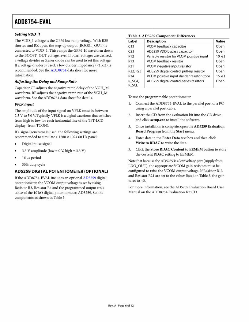
AD5259 DIGITAL POTENTIOMETER (OPTIONAL) If the ADD8754-EVAL includes an optional AD5259 digital potentiometer, the VCOM output voltage is set by using Resistor R3, Resistor R4 and the programmed output resis- tance of the 10 kΩ digital potentiometer, AD5259. Set the components as shown in Table 3.
Table 3. AD5259 Component Differences Label Description Value C13 VCOM feedback capacitor Open C23 AD5259 VDD bypass capacitor Open R12 Variable resistor for VCOM positive input 10 kΩ R13 VCOM feedback resistor Open R21 VCOM negative input resistor Open R22, R23 AD5259 digital control pull-up resistor Open R24 VCOM positive input divider resistor (top) 15 kΩ R_SCA, R_SCL
AD5259 digital control series resistors Open
To use the programmable potentiometer
1. Connect the ADD8754-EVAL to the parallel port of a PC using a parallel port cable.
2. Insert the CD from the evaluation kit into the CD drive and click setup.exe to install the software.
3. Once installation is complete, open the AD5259 Evaluation Board Program from the Start menu.
4. Enter data in the Enter Data text box and then click Write to RDAC to write the data.
5. Click the Store RDAC Content to EEMEM button to store the current RDAC setting to EEMEM.
Note that because the AD5259 is a low voltage part (supply from LDO_OUT), the appropriate VCOM gain resistors must be configured to raise the VCOM output voltage. If Resistor R13 and Resistor R21 are set to the values listed in Table 3, the gain is set to +3.
For more information, see the AD5259 Evaluation Board User Manual on the ADD8754 Evaluation Kit CD.

ADD8754-EVAL
Rev. A | Page 7 of 12
EVALUATION BOARD LAYOUT FUNCTIONAL BLOCKS
BLOCK 1
BLOCK 2
BLOCK 10
BLOCK 3
BLOCK 4
BLOCK 8
BLOCK 7
BLOCK 6
BLOCK 9
BLOCK 5
0604
0-00
6
Figure 6. Evaluation Board Layout
Table 4. Evaluation Board Functional Block Descriptions Block Description 1 Positive Charge Pump. Provides access to the positive charge pump output (VCPH) and ground. 2 Gate Pulse Modulation. Accepts digital inputs from the timing controller (TCON) and provides a modulated VGH waveform (VGH_M). 3 VCOM Amplifiers. Provides access to the VCOM amplifier. The potentiometer in Block 9 adjusts the VCOM voltage. 4 AD5259 Serial Port. Accepts a serial port. Only boards with the optional AD5259 digital potentiometer include this port. 5 LDO. Provides access to the LDO output. 6 Digital Potentiometer. For digital control of the AD5259. Only boards equipped with the optional AD5259 use this pin. 7 Power Supply. Accepts an input voltage and provides the step-up output voltage (BOOST_OUT) and various ground pins. 8 Negative Charge Pump. Provides access to the negative charge pump output (VCPL) and ground. 9 VCOM Potentiometer. Includes one analog potentiometer configured in a rheostat mode for VCOM adjustment. 10 ADD8754. Includes a soldered ADD8754 24-lead LFCSP. If the part needs to be replaced, care should be taken to properly solder
the thermal vias to the thermal pad on the bottom side of the IC.

ADD8754-EVAL
Rev. A | Page 8 of 12
LAYERS
0604
0-00
7
Figure 7. Evaluation Board Layout—Top Layer

ADD8754-EVAL
Rev. A | Page 9 of 12
0604
0-00
8
Figure 8. Evaluation Board Layout—Bottom Layer
Table 5. Evaluation Board Layer Descriptions Layer Description Blue (Top) Top-of-board metal traces and ground plane. See Figure 7. Red (Bottom) Bottom-of-board metal traces and ground plane. Note that the top-view is shown in Figure 8. Silkscreen text is shown for
orientation purposes only; text does not appear on bottom of board.

ADD8754-EVAL
Rev. A | Page 10 of 12
SCHEMATIC
0604
0-00
9
Figure 9. Evaluation Board

ADD8754-EVAL
Rev. A | Page 11 of 12
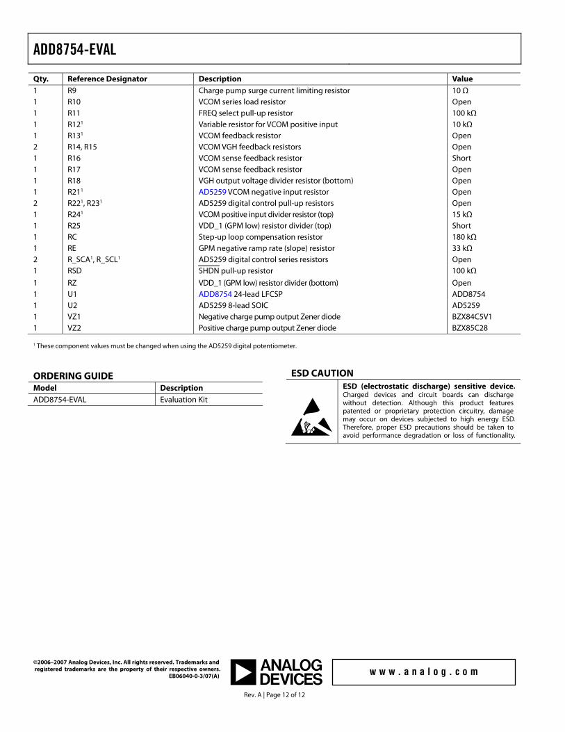
ORDERING INFORMATION COMPONENT LISTING
Table 6. Qty. Reference Designator Description Value 2 C1, C2 Positive charge pump flying capacitors 0.1 μF 2 C3, C4 Positive charge pump charging capacitors 1 μF 1 C5 Negative charge pump flying capacitor 0.1 μF 1 C6 Negative charge pump charging capacitor 1 μF 1 C7 Negative charge pump filter capacitor 1 μF 1 C8 VPDM start-up delay capacitor Open 1 C9 VCOM load capacitor Open 1 C10 VDD_2 (VCOM supply) bypass capacitor 0.1 μF 1 C11 VDD_1 (GPM low) bypass capacitor 0.1 μF 1 C12 LDO output bypass capacitor 0.1 μF 1 C131 VCOM feedback capacitor Open 2 C14, C15 VCOM VGH feedback capacitors Open 1 C16 VCOM sense feedback capacitor Short 1 C17 VCOM sense feedback capacitor Open 1 C18 VCOM positive input bypass capacitor 4.7 μF 1 C22 VCOM feedback capacitor Open 1 C231 AD5259 VDD bypass capacitor Open 1 C24 VDD_1 filter capacitor Open 1 CC Step-up loop compensation capacitor 470 pF 1 CC1 Step-up loop compensation capacitor 30 pF 1 CE GPM negative ramp delay capacitor 1 nF 1 CIN VIN_1 and VIN_2 bypass capacitor 10 μF 1 CIN1 VIN_1 bypass capacitor 0.1 μF 1 CIN2 VIN_2 bypass capacitor 0.1 μF 1 CLDO LDO output capacitor 4.7 μF 2 COUT1, COUT2 Step-up output (charging) capacitors 10 μF 1 COUT3 Step-up output capacitor 0.1 μF 1 CSS Soft-start capacitor 10 nF 1 D1 Step-up converter diode 1N5818 2 D2/D3 Positive charge pump doubler diodes BAV99WT1 2 D4/D5 Positive charge pump tripler diodes BAV99WT1 2 D6/D7 Negative charge pump diodes BAV99WT1 1 FUSE Input supply fuse 1A 1 JP1 SHDN jumper Open
1 JP2 FREQ select jumper Short 1 JP3 LDO output select jumper Short 1 and Short 2 1 JP4 VCOM buffer configuration jumper Short 1 JP5 VDPM from step-up jumper Short 1 JP6 VCOM supply from step-up jumper Short 1 JP7 Positive charge pump to VGH Short 1 L1 Step-up converter inductor 10 μH 1 R1 Step-up feedback divider resistor (top) 71.5 kΩ 1 R2 Step-up feedback divider resistor (bottom) 10 kΩ 1 R31 AD5259 divider resistor (top) Open 1 R4 VCOM positive input divider resistor (bottom) 20 kΩ 1 R5 Positive charge pump current limiting resistor 1 kΩ 1 R6 Negative charge pump current limiting resistor 300 Ω 1 R7 VDPM step-up voltage divider resistor (top) 47 kΩ 1 R8 VDPM step-up voltage divider resistor (bottom) 8.2 kΩ
ADD8754-EVAL
Rev. A | Page 12 of 12
Qty. Reference Designator Description Value 1 R9 Charge pump surge current limiting resistor 10 Ω 1 R10 VCOM series load resistor Open 1 R11 FREQ select pull-up resistor 100 kΩ 1 R121 Variable resistor for VCOM positive input 10 kΩ 1 R131 VCOM feedback resistor Open 2 R14, R15 VCOM VGH feedback resistors Open 1 R16 VCOM sense feedback resistor Short 1 R17 VCOM sense feedback resistor Open 1 R18 VGH output voltage divider resistor (bottom) Open 1 R211 AD5259 VCOM negative input resistor Open 2 R221, R231 AD5259 digital control pull-up resistors Open 1 R241 VCOM positive input divider resistor (top) 15 kΩ 1 R25 VDD_1 (GPM low) resistor divider (top) Short 1 RC Step-up loop compensation resistor 180 kΩ 1 RE GPM negative ramp rate (slope) resistor 33 kΩ 2 R_SCA1, R_SCL1 AD5259 digital control series resistors Open 1 RSD SHDN pull-up resistor 100 kΩ
1 RZ VDD_1 (GPM low) resistor divider (bottom) Open 1 U1 ADD8754 24-lead LFCSP ADD8754 1 U2 AD5259 8-lead SOIC AD5259 1 VZ1 Negative charge pump output Zener diode BZX84C5V1 1 VZ2 Positive charge pump output Zener diode BZX85C28 1 These component values must be changed when using the AD5259 digital potentiometer.
ORDERING GUIDE Model Description ADD8754-EVAL Evaluation Kit
ESD CAUTION
©2006–2007 Analog Devices, Inc. All rights reserved. Trademarks and registered trademarks are the property of their respective owners. EB06040-0-3/07(A)