Embed Size (px)
Citation preview
Adaptive Multilevel Quadrature Amplitude Radio Implementation in Programmable Logic
A Thesis Submitted to the College of
Graduate Studies and Research
in Partial Fulfillment of the Requirements
For the Degree of Master of Science
in the Department of Electrical Engineering
University of Saskatchewan
Saskatoon, Saskatchewan
by
Daniel Aspel
© Copyright Daniel Aspel, April 2004. All Rights Reserved

ii
Permission To Use
In presenting this thesis in partial fulfillment of the requirements for a
Postgraduate degree for the University of Saskatchewan, I agree that the Libraries of this
University may make it freely available for inspection. I further agree that permission for
copying of this thesis in any manner, in whole or in part, for scholarly purposes may be
granted by the professor or professors who supervised my thesis work, or in their
absence, by the Head of the Department or the Dean of the College in which my thesis
work was done. It is understood that any copying, publication, or use of this thesis or
parts thereof for financial gain shall not be allowed without my written permission. It is
also understood that due recognition shall be given to me and the University of
Saskatchewan in any scholarly use which may be made of any material in my thesis.
Requests for permission to copy or to make use of material in this thesis in whole
or part should be addressed to:
Head of the Department of Electrical Engineering
University of Saskatchewan
Saskatoon, Saskatchewan, Canada
S7N 5A9

iii
Abstract Emerging broadband wireless packet data networks are increasingly employing
spectrally efficient modulation methods like Quadrature Amplitude Modulation (QAM)
to increase the channel efficiency and maximize data throughput. Unfortunately, the
performance of high level QAM modulations in the wireless channel is sensitive to
channel imperfections and throughput is degraded significantly at low signal-to-noise
ratios due to bit errors and packet retransmission. To obtain a more “robust” physical
layer, broadband systems are employing multilevel QAM (M-QAM) to mitigate this
reduction in throughput by adapting the QAM modulation level to maintain acceptable
packet error rate (PER) performance in changing channel conditions.
This thesis presents an adaptive M-QAM modem hardware architecture, suitable
for use as a modem core for programmable software defined radios (SDRs) and
broadband wireless applications. The modem operates in “burst” mode, and can reliably
synchronize to different QAM constellations “burst-by-burst”.
Two main improvements exploit commonality in the M-QAM constellations to
minimize the redundant hardware required. First, the burst synchronization functions
(carrier, clock, amplitude, and modulation level) operate reliably without prior knowledge
of the QAM modulation level used in the burst. Second, a unique bit stuffing and shifting
technique is employed which supports variable bit rate operation, while reducing the core
signal processing functions to common hardware for all constellations. These features
make this architecture especially attractive for implementation with Field Programmable
Gate Arrays (FPGAs) and Application-Specific Integrated Circuits (ASICs); both of
which are becoming popular for highly integrated, cost-effective wireless transceivers.

iv
Acknowledgements
The author thanks his supervisor, Dr. David Klymyshyn, for his guidance and
support throughout the preparation of this thesis.
The author would also like to thank the management and staff of
Telecommunications Research Laboratories (TRLabs) for the use of their facilities and
technical assistance during the research work. Thanks are extended to SaskTel for
financial assistance throughout the duration of the research.
I would also like to thank my family and friends for their support throughout this
project. In particular, I would like to thank my fiancée, Heather, for her love and support
throughout my graduate program.

v
Table of Contents
Permission To Use ................................................................................................... ii
Abstract ................................................................................................................... iii
Acknowledgements................................................................................................. iv
Table of Contents..................................................................................................... v
List of Tables........................................................................................................... ix
List of Figures .......................................................................................................... x
List of Abbreviations............................................................................................ xiv
1 Introduction ............................................................................................................. 1
1.1 Wireless Communications and the Internet ..................................................... 1
1.2 Broadband Wireless Internet Access ............................................................... 2
1.3 Software Defined Radios ................................................................................. 3
1.4 Research Motivation ........................................................................................ 5
1.5 Research Objectives......................................................................................... 6
1.6 Literature Review............................................................................................. 7
1.7 Thesis Organization ......................................................................................... 8
2 Modulation and Modem Theory .......................................................................... 10
2.1 Modulation..................................................................................................... 10
2.2 Quadrature Amplitude Modulation................................................................ 12
2.3 Multilevel Quadrature Amplitude Modulation .............................................. 13
2.4 Sampling Theory............................................................................................ 16
2.4.1 Upsampling ........................................................................................ 18
2.4.2 Downsampling ................................................................................... 19
2.4.3 Undersampling................................................................................... 21
2.5 Digital to Analog Conversion ........................................................................ 21
2.6 Digital QAM Transmitter .............................................................................. 24
2.7 Digital QAM Receiver ................................................................................... 26
3 M-QAM Transceiver Architecture...................................................................... 28

vi
3.1 Overview........................................................................................................ 28
3.2 System Architecture....................................................................................... 29
3.3 Burst-Mode M-QAM Transmitter ................................................................. 30
3.4 Burst-Mode M-QAM Receiver...................................................................... 31
3.5 Bit Stuffing and Shifting................................................................................ 33
3.5.1 Packet Generator ................................................................................ 33
3.5.2 Gray Coding and Bit Stuffing ............................................................ 34
3.5.3 Mapping and Shifting ........................................................................ 35
3.6 Burst Format .................................................................................................. 36
3.7 Detecting the Burst ........................................................................................ 37
3.8 Detecting the Data Segment........................................................................... 38
3.9 Modulation Level........................................................................................... 38
3.10 Burst Length................................................................................................... 39
4 Automatic Gain Control ....................................................................................... 40
4.1 Overview........................................................................................................ 40
4.2 Effect of Amplitude Variation ....................................................................... 41
4.3 Burst Mode AGC ........................................................................................... 42
4.4 Feed-Forward AGC vs. Feedback AGC ........................................................ 42
4.5 Feedback AGC Implementation .................................................................... 44
4.5.1 Bin Size Calculation (Preamble)........................................................ 45
4.5.2 Bin Size Calculation (Random M-QAM Data) ................................. 46
4.6 Functional Verification of the AGC Subsystem ............................................ 47
5 Symbol Timing Recovery...................................................................................... 49
5.1 Overview........................................................................................................ 49
5.2 Symbol Timing Recovery Techniques........................................................... 50
5.2.1 Times-Two Symbol Timing Recovery .............................................. 51
5.2.2 Maximum Amplitude Symbol Timing Recovery .............................. 51
5.2.3 Early-Late Symbol Timing Recovery................................................ 52
5.2.4 Zero Crossing Symbol Timing Recovery .......................................... 53
5.3 Predicted Edge Crossing Symbol Timing Recovery System......................... 54
5.3.1 Phase Detector ................................................................................... 55

vii
5.3.2 N Counter........................................................................................... 59
5.3.3 K Counter and Control Logic ............................................................ 59
5.3.4 Symbol Timing Frequency Offsets .................................................... 60
5.4 Functional Verification of the Symbol Timing Recovery Subsystem ........... 61
6 Carrier Recovery................................................................................................... 63
6.1 Overview........................................................................................................ 63
6.2 Need For Carrier Recovery............................................................................ 63
6.3 Carrier Recovery Techniques ........................................................................ 65
6.3.1 Pilot Tone Assisted Carrier Recovery................................................ 65
6.3.2 Squaring Loop.................................................................................... 66
6.3.3 Costas Loop ....................................................................................... 66
6.3.4 Decision Feedback Phase Locked Loop ............................................ 67
6.4 Implementation of a Decision Feedback PLL ............................................... 68
6.4.1 Derotator ............................................................................................ 68
6.4.2 Phase Detector ................................................................................... 69
6.4.3 Quadrant Ambiguity .......................................................................... 73
6.4.4 Loop Filter and Phase Accumulator .................................................. 73
6.5 Functional Verification of the Carrier Recovery Subsystem......................... 74
7 Filtering .................................................................................................................. 76
7.1 Overview........................................................................................................ 76
7.2 Finite Impulse Response Filters..................................................................... 77
7.3 Square Root Raised Cosine Filters ................................................................ 77
7.3.1 Transmit RRC Filter .......................................................................... 80
7.3.2 Receive RRC Filter ............................................................................ 82
7.4 IF Filters......................................................................................................... 83
7.4.1 Halfband Filter Design....................................................................... 84
7.4.2 Sin(x)/x Correction and Analog Filter Correction ............................. 85
7.5 Reconstruction Filter...................................................................................... 85
7.6 Prediction Filter ............................................................................................. 86
7.7 Digital Filter Implementation ........................................................................ 87
7.8 Canonical Signed Digit Multiplier Filters...................................................... 88

viii
7.9 Serial Filters ................................................................................................... 88
7.10 Symbol Timing Phase Adjustment ................................................................ 90
7.11 Transmitted Spectrum.................................................................................... 91
8 Implementation and Performance Results.......................................................... 92
8.1 Overview........................................................................................................ 92
8.2 TRLabs FPGA Development system............................................................. 94
8.3 Channel .......................................................................................................... 94
8.4 FPGA Logic Utilization and Layout.............................................................. 95
8.5 Bit Error Rate Results .................................................................................... 99
8.6 Packet Error Rate ......................................................................................... 101
8.7 Effect of Carrier Frequency Offsets on BER............................................... 105
8.8 Effect of Symbol Timing Frequency Offsets on BER ................................. 108
8.9 Effect of Amplitude Variation on BER ....................................................... 111
8.10 Effect of Packet Length on BER.................................................................. 114
9 Summary and Conclusions ................................................................................. 118
9.1 Summary of Objectives................................................................................ 118
9.2 Summary of Results and Conclusion........................................................... 120
9.3 Recommendations for Future Study ............................................................ 121
References ............................................................................................................ 123
A Verilog Code ........................................................................................................ 126
B Matlab Code......................................................................................................... 128

ix
List of Tables
Table 8.1: Modem Implementation ................................................................................. 96
Table 8.2: Transmitter Implementation ........................................................................... 96
Table 8.3: IF Filtering Implementation............................................................................ 96
Table 8.4: Receiver Implementation................................................................................ 96
Table 8.5: Test Module Implementation.......................................................................... 98
Table A.1: Verilog Source Code Tree ........................................................................... 127
Table B.1: Matlab Source Code Tree ............................................................................ 129

x
List of Figures
Figure 2.1: Constellation for a PAM Signal .................................................................... 11
Figure 2.2: Time Domain Envelope of a PAM Signal .................................................... 11
Figure 2.3: Constellation for a QAM Signal.................................................................... 13
Figure 2.4: QAM Constellations...................................................................................... 14
Figure 2.5: Theoretical QAM BER.................................................................................. 15
Figure 2.6: Sampled Waveforms ..................................................................................... 17
Figure 2.7: Time Domain View of Upsampling .............................................................. 18
Figure 2.8: Frequency Domain View of Upsampling...................................................... 19
Figure 2.9: Time Domain View of Downsampling ......................................................... 20
Figure 2.10: Frequency Domain View of Downsampling............................................... 20
Figure 2.11: Frequency Domain View of Undersampling .............................................. 21
Figure 2.12: D/A Output .................................................................................................. 22
Figure 2.13: D/A Effects.................................................................................................. 23
Figure 2.14: Reconstruction Filtering.............................................................................. 23
Figure 2.15: Digital QAM Transmitter............................................................................ 24
Figure 2.16: Gray Coding ................................................................................................ 25
Figure 2.17: Digital QAM Receiver ................................................................................ 26
Figure 3.1: System Architecture ...................................................................................... 29
Figure 3.2: Burst-Mode M-QAM Transmitter................................................................. 30
Figure 3.3: Burst-Mode M-QAM Receiver ..................................................................... 32
Figure 3.4: Bit Stuffing and Gray Coding/Decoding for QAM-16 (N/2=2, Nmax/2=3)... 34
Figure 3.5: Mapper Input and Mapped Levels for QAM-16 (N/2=2, Nmax/2=3) ............ 35
Figure 3.6: Burst Format.................................................................................................. 36
Figure 3.7: Preamble Point Selections for QAM-64........................................................ 36
Figure 3.8: Frame Synchronizer ...................................................................................... 37
Figure 4.1: Bin Size ......................................................................................................... 41
Figure 4.2: Scaled PAM Constellations........................................................................... 41

xi
Figure 4.3: Feed-Forward AGC....................................................................................... 43
Figure 4.4: Feedback AGC .............................................................................................. 43
Figure 4.5: Amplitude Detection Block........................................................................... 44
Figure 4.6: Constellations for QAM-4, QAM-16, and QAM-64 with Possible Preamble
Symbols Highlighted ................................................................................................ 45
Figure 4.7: AGC For Random Data................................................................................. 47
Figure 4.8: Operation of the AGC ................................................................................... 48
Figure 5.1: Sampling........................................................................................................ 50
Figure 5.2: Average Symbol Amplitude as a Function of Time...................................... 52
Figure 5.3: Early-Late Sampling ..................................................................................... 53
Figure 5.4: QAM-4 Eye Diagram .................................................................................... 53
Figure 5.5: Simplified Zero Crossing Symbol Timing Recovery Implementation ......... 55
Figure 5.6: Sampled Points for I and Q for a QAM-4 Signal .......................................... 56
Figure 5.7: Zero Crossing Jitter ....................................................................................... 57
Figure 5.8: Expected Edge Values................................................................................... 58
Figure 5.9: Adjustable K Counter.................................................................................... 60
Figure 5.10: Second Order K Counter ............................................................................. 61
Figure 5.11: Operation of the Symbol Timing Recovery Subsystem.............................. 62
Figure 6.1: Effect of Carrier Phase and Frequency Offset............................................... 64
Figure 6.2: Signal with Embedded Pilot Tone................................................................. 65
Figure 6.3: Square-Law Based PLL for Carrier Recovery .............................................. 66
Figure 6.4: Costas Loop................................................................................................... 67
Figure 6.5: Decision Feedback PLL for QAM ................................................................ 67
Figure 6.6: Decision Feedback PLL Carrier Recovery for QAM with Derotator ........... 68
Figure 6.7: Derotator Implementation ............................................................................. 69
Figure 6.8: Quadrant Rotation ......................................................................................... 70
Figure 6.9: Probability Distribution of Phase Error Calculation Error............................ 72
Figure 6.10: Loop Filter Block Implementation .............................................................. 74
Figure 6.11: Operation of the Carrier Recovery Subsystem............................................ 75
Figure 7.1: Raised Cosine Filter Frequency Response .................................................... 78
Figure 7.2: Raised Cosine Filter Impulse Response ........................................................ 79

xii
Figure 7.3: RRC Filter Impulse Response ....................................................................... 79
Figure 7.4: Transmit RRC Filter Impulse Response........................................................ 81
Figure 7.5: Transmit RRC Filter Frequency Response.................................................... 81
Figure 7.6: Receive RRC Filter Impulse Response ......................................................... 82
Figure 7.7: Receive RRC Filter Frequency Response ..................................................... 83
Figure 7.8: TX IF Filtering .............................................................................................. 84
Figure 7.9: RX IF Filtering .............................................................................................. 84
Figure 7.10: Reconstruction Filter .................................................................................... 85
Figure 7.11: Receive RRC Filter Impulse Resonse ......................................................... 86
Figure 7.12: FIR Filter ...................................................................................................... 87
Figure 7.13: Symmetric FIR Filter ................................................................................... 87
Figure 7.14: Serial FIR Filter............................................................................................ 89
Figure 7.15: Modified Shift Register ................................................................................ 89
Figure 7.16: Shift Register, Offset Shift Register............................................................ 90
Figure 7.17: Transmitted Spectrum .................................................................................. 91
Figure 8.1: Implemented System Architecture ................................................................ 92
Figure 8.2: TRLabs FPGA Development Board .............................................................. 94
Figure 8.3: AWGN Channel ............................................................................................. 95
Figure 8.4: FPGA Floor Plan of the 600,000 Gate APEX FPGA .................................... 97
Figure 8.5: BER Results (Worst-case Receive Amplitude Level).................................. 100
Figure 8.6: PER Results (Undetected Packets)............................................................... 102
Figure 8.7: PER Results for Detected QAM-4 Packets .................................................. 103
Figure 8.8: PER Results for Detected QAM-16, QAM-64 and QAM-256 Bursts ......... 104
Figure 8.9: Effect of Carrier Offset on BER................................................................... 107
Figure 8.10: Effect of Carrier Offset on PER ................................................................. 108
Figure 8.11: Effect of Symbol Timing Frequency Offset on BER................................. 109
Figure 8.12: Effect of Symbol Timing Frequency Offset on PER ................................. 110
Figure 8.13: Effect of Amplitude Variation on QAM-256 BER .................................... 112
Figure 8.14: Effect of Amplitude Variation on QAM-64 BER ...................................... 112
Figure 8.15: Effect of Amplitude Variation on QAM-16 BER ...................................... 112
Figure 8.16: Distribution of Bit Errors ........................................................................... 114
xiii
Figure 8.17: Distribution of Bit Errors (Carrier Frequency Offset) ............................... 115
Figure 8.18: Carrier Recovery Gain Differences............................................................ 116
Figure 8.19: Distribution of Bit Errors (Symbol Timing Frequency Offset).................. 116

xiv
List of Abbreviations
A/D Analog to Digital
AGC Automatic Gain Control
ARPA Advanced Research Projects Agency
ASIC Application Specific Integrated Circuit
AWGN Additive White Gaussian Noise
BER Bit Error Rate
BWA Broadband Wireless Access
CSD Canonical Signed Digit
D/A Digital to Analog
DBPSK Differential Binary Phase Shift Keying
DC Direct Current
DOCSIS Data Over Cable Service Interface Specification
DPLL Digital Phase Locked Loop
DSL Digital Subscriber Line
DSLAM Digital Subscriber Line Access Multiplexer
DSP Digital Signal Processor
Email Electronic Mail
ESB Embedded System Block
EVM Error Vector Magnitude
FEC Forward Error Correction
FIFO First In First Out
FIR Finite Impulse Response
FPGA Field Programmable Gate Array
HDL Hardware Description Language
I In-phase
IEEE Institute of Electrical and Electronics Engineers
IF Intermediate Frequency
IP Internet Protocol

xv
ISI Inter-Symbol Interference
LAB Logic Array Block
LSB Least Significant Bit
M-QAM Multi-level Quadrature Amplitude Modulation
NCO Numerically Controlled Oscillator
NCSA National Center for Supercomputing Applications
NRE Non-Recurring Engineering
PAM Pulse Amplitude Modulation
PDF Probability Distribution Function
PER Packet Error Rate
PLL Phase Locked Loop
PN Pseudo-random Noise
PSD Power Spectral Density
Q Quadrature
QAM Quadrature Amplitude Modulation
RC Raised Cosine
RMS Root Mean Square
RRC Root-Raised Cosine
SAW Surface Acoustic Wave
SDR Software Defined Radio
SNR Signal-to-Noise Ratio
SRAM Static Random Access Memory
TDD Time Division Duplexing
TDM Time Division Multiplexing
VCO Voltage Controlled Oscillator
VHDL Very High Speed Integrated Circuit Hardware Description Language
WWW World Wide Web

1
Chapter 1
Introduction
1.1 Wireless Communications and the Internet
Wireless communication allows information to be transmitted via radio waves.
The first successful wireless transmission of information occurred in 1895 [1]. Initially,
wireless communications were used primarily by the military and for radio broadcasting.
Today, wireless communications technologies are used for cellular telephony, radio
broadcasting, broadcast television, and many other applications. An emerging and
increasingly important use of wireless communications is for the provision of Internet
connectivity.
The Internet was created in 1969 by a division of the United States Department of
Defense, the Advanced Research Projects Agency (ARPA). The Internet originally
connected computers at four universities in the southwestern United States [2]. Within
months, more research institutions were added.
The Internet was initially difficult to use and was used only by computer experts.
Slowly, applications for electronic mail (email) and file transfer were developed that
allowed non-technical people to use the Internet. Between 1989 and 1991, Tim Berners-
Lee and Robert Cailliau developed a technique for linking documents on the Internet
while working at CERN. The network of “hyperlinked web pages” became known as the
World Wide Web (WWW). In 1993, Marc Andreessen and his team at the National
Center for Supercomputing Applications (NCSA) developed the graphical browser
Mosaic [2]. Mosaic allowed people with no technical knowledge to browse the World
Wide Web. Today, many applications exist that use the Internet for communication.
These applications range from mature applications such as email and web browsing to

2
cutting- edge applications for database access, gaming, electronic commerce, voice
communications, and video delivery.
Today most Internet users connect to the Internet using a dial-up connection on a
phone line, a Digital Subscriber Line (DSL), or a cable modem. Dial-up connections are
limited to 56kb/s. DSL and cable modems provide much higher speed access; however,
the serving areas for these technologies are limited by their infrastructure. Cable service
is limited by the footprint of the cable network. DSL service is limited to 4km to 5km
from a central office or a remote Digital Subscriber Line Access Multiplexer (DSLAM).
An alternative to using wired Internet service is to use a wireless connection to
connect the user to the Internet. Satellite service is one option for this task; however, it is
very costly. Both second generation cellular telephony and third generation cellular
telephony provide options for connection to the Internet; however, these options can be
costly and bandwidth is limited to a range from tens of kilobits per second up to several
megabits per second shared within a cell. Broadband wireless access provides a higher
bandwidth alternative.
1.2 Broadband Wireless Internet Access
Broadband Wireless Access (BWA) can provide reliable high rate Internet access.
The bandwidth provided by BWA can be comparable to DSL and cable systems.
Furthermore, BWA can be advantageous where current infrastructure does not support
high-rate Internet access, where it is not feasible to deploy wired infrastructure, or where
rapid deployment is desirable.
BWA can be deployed in both point-to-point and point-to-multipoint formats.
Point-to-point installations provide the highest bandwidth to a user because directional
antennas provide the best signal strength and the bandwidth is not shared among multiple
users. To reduce cost, a single base station can be shared among multiple users in a
point-to-multipoint configuration to provide a more economical cellular arrangement
while still maintaining bandwidths in the same order of magnitude as those provided by
cable modems and DSL.
Point-to-multipoint communications systems typically share one or more radio
channels between multiple users. The systems can be classified into two categories based

3
on how the channel or channels are used: Time Division Multiplexing (TDM) systems or
Time Division Duplexing (TDD) systems.
TDM systems typically use two radio channels: one for “downstream”
information that flows from the base station to the users and one for “upstream”
information that flows from the users to the base station. TDM systems get their name
from the fact that downstream information destined for multiple users is multiplexed in
time onto the downstream channel while the upstream information from all of the users is
multiplexed onto the upstream channel.
TDD systems typically use only one channel that is used for both upstream and
downstream information. Thus, the TDD systems get their name from the duplexing of
upstream and downstream information onto a single channel. TDD systems also permit
efficient use of the radio channel because the ratio of channel bandwidth allocated for
upstream traffic to the channel bandwidth allocated for downstream traffic can be
changed dynamically whereas TDM systems typically have a fixed ratio of upstream to
downstream bandwidth. The variable ratio of upstream to downstream bandwidth is
particularly important for web surfing and other Internet applications that have bursty and
asymmetric bandwidth requirements.
TDD systems do not transmit continuously. Instead, TDD systems operate in
burst-mode where they transmit blocks of information and then remain silent listening to
the channel until they transmit again. To receive a burst of information, the receiver must
synchronize to the burst. Synchronizing to the burst is called frame synchronization.
Frame synchronization is facilitated by a preamble that is appended to the beginning of
each burst.
1.3 Software Defined Radios
In the past, communications systems have typically been implemented using
discrete analog components. These systems tended to be complicated to build and
difficult to tune. Furthermore, if any aspect of the communication system needed to be
changed, physical components in the system needed to be replaced with new components
to perform the changed operation.

4
Digital signal processing techniques extended the capabilities of radio systems by
allowing the use of more complicated modulation and demodulation techniques. Initially
Application Specific Integrated Circuits (ASICs) were used for this task. Unfortunately,
ASICs incur large Non-Recurring Engineering (NRE) expenses for design and
fabrication. Furthermore, ASICs cannot be modified. Therefore, if a change is required
to an ASIC, large NRE expenses are incurred again.
More recent trends have been to implement the digital signal processing functions
in a Digital Signal Processor (DSP) or a Field Programmable Gate Array (FPGA). Both
DSPs and FPGAs are programmed using abstract programming languages. Therefore,
the modems that they implement have been termed Software Defined Radios (SDRs).
SDRs have grown in popularity due to their ability to be reprogrammed in the field to
support new and updated standards.
Both DSPs and FPGAs can be easily reprogrammed without replacing or
fabricating new devices. This programmability results in much lower NRE expenses for
DSPs and FPGAs than ASICs. Additionally, many of the DSP and FPGA-based software
defined radios can be completely, or partially, reprogrammed in the field. This results in
modems that can be reconfigured for multiple modulation schemes [3].
An FPGA consists of programmable logic blocks and pins that allow the FPGA to
connect other circuit elements. The logic blocks are connected to each other and the pins
by programmable interconnect. By connecting the inputs of the logic blocks, the outputs
of the logic blocks, and the pins with the programmable interconnect, the FPGA can be
configured to perform arbitrary logic operations.
FPGAs are configured using a Hardware Description Language (HDL) such as
Verilog or VHDL (Very high speed integrated circuit Hardware Description Language).
Verilog and VHDL differ from typical procedural programming languages such as C
because they directly or indirectly define a circuit layout whereas C defines a series of
operations to be performed. This results in an easy transition from data path functional
blocks to logic blocks in the FPGA. Furthermore, functional blocks in a system design
can be easily mapped into discrete areas in an FPGA [4, 5].
FPGAs are particularly attractive for SDRs because of the ease and speed of
which they can be reprogrammed. FPGAs can be programmed by simply loading new

5
configuration information into the FPGA from a computer or a memory device which is
permanently connected to the FPGA.
1.4 Research Motivation
The initial motivation for this research was to develop a modem architecture
suitable for use in a TDD BWA system. The main criterion in the selection process was
to find an efficient modem implementation that could maintain high data throughput over
a wide range of Signal-to-Noise Ratios (SNRs).
Choosing a modulation scheme for a modem can involve many tradeoffs. The
error rate for a modulation scheme depends on the constellation used by the modem and
the ability of the receiver to synchronize to the received signal with the presented channel
impairments. The constellation is a representation of the amplitude and phase of all
possible data symbols that are transmitted. Constellations range from simple
constellations with two symbols of equal amplitude and 180 degrees difference in phase
to complex constellations with hundreds of symbols that have many different amplitudes
and phases.
Obtaining the highest data throughput for packetized data is complicated by noise
in the radio channel. While complex constellations can transmit more information in a
given bandwidth, they also have higher bit error rates at a given SNR resulting in more
packets that must be retransmitted due to errors. Therefore, the constellation must be
chosen to optimize data throughput subject to the amount of information that can be
transmitted in the chosen bandwidth and the probability of packets being discarded.
However, the probability of packets being discarded varies with the SNR in a wireless
channel, which is often highly variable. Therefore, this research looks at using multiple
constellations that can be chosen to optimize the data throughput: simple constellations
when the SNR is low and complex constellations when the SNR is high.
Emerging broadband wireless packet data networks are increasingly employing
spectrally efficient modulation methods like Quadrature Amplitude Modulation (QAM)
to increase the channel efficiency and maximize data throughput. However, the
performance of high level QAM modulations is sensitive to conditions in the wireless
channel and throughput can be degraded significantly due to bit errors and packet

6
retransmission. Increasingly, these systems are being designed to revert to simpler
constellations when packet error rates reach a certain level. These systems have a
number of drawbacks because of the extra modem complexity required to support
different constellations. Furthermore, these systems cannot generally adapt on a burst-
by-burst or user-by-user basis.
To overcome the impediments associated with high level QAM constellations,
broadband standards like the Institute of Electrical and Electronics Engineers (IEEE)
802.16 standard [6, 7] are employing Multilevel QAM (M-QAM) to mitigate this
reduction in throughput by adapting the QAM modulation level to maintain acceptable
Packet Error Rate (PER) performance in changing channel conditions. These newer
standards and systems are employing the use of different QAM constellations for
different users based on the channel conditions for those users. They are also changing
those constellations as the channel conditions change over time.
1.5 Research Objectives
The goal of this research was to develop and test an adaptive M-QAM modem
hardware architecture suitable for use as a modem core for SDRs and broadband wireless
applications where the SNR can vary over a wide range. A number of objectives were
identified to meet this goal.
The first objective was to develop burst mode capabilities such that each burst
could be received independently of all other bursts. Burst mode operation allows the
modem to operate in a TDD system. Furthermore, burst operation allows each burst to be
modulated with a constellation that is most appropriate for the channel conditions
between the source and destination at the point in time when the burst is transmitted.
The second objective was to research, implement, and test synchronization
methods that would be appropriate for synchronization with multiple QAM constellations
over a wide range of SNRs. The carrier, clock, amplitude, frame, and modulation level
synchronization functions were to operate reliably without prior knowledge of the QAM
modulation level used in the burst. The synchronization functions must operate quickly
to synchronize with the received packet during a short preamble and to track the
synchronization parameters throughout the data segment of the burst. Furthermore, the

7
receiver must correctly synchronize to a high percentage of bursts and the
synchronization loops must maintain accurate synchronization regardless of the SNR.
The third objective was to exploit commonality in the M-QAM constellations to
minimize the redundant hardware required. The commonality in the different QAM
constellations was to be used to allow multiple subsystems to operate on multiple
constellations without modifying their operation or duplicating modules.
The fourth objective was to compare the performance of the modem to theoretical
performance limits using a simulated radio channel. The modem performance was to be
determined using numerical simulation and measurements on the hardware
implementation.
1.6 Literature Review
An overview of QAM modulation can be found in many textbooks such as those
by Couch [8], Webb [9], and Proakis [10]. As well, a number of digital QAM
architectures have been described in literature. A paper by Daneshrad and Samueli [11]
describes an ASIC implementation of a digital QAM modem. Currently there are
M-QAM modems being developed and deployed that meet the Data Over Cable Service
Interface Specification (DOCSIS) [12] and IEEE 802.16 [6, 7] specifications. For
example, a DOCIS compliant M-QAM modem is described in literature by D’Luna et al.
[13].
Papers on SDRs have been written by Honda [3], Mintzer [4], and Gun et al. [14].
Cummings and Haruyama [15] discuss the implementation tradeoffs for SDRs
implemented in DSPs and FPGAs. Gun et al. describes implementation tradeoffs for
software radio architectures. The paper by Honda describes an FPGA-based QAM
modem that is partially reconfigurable on-the-fly. Mintzer describes a QAM transmitter
designed for an FPGA. Other papers that describe SDRs include Hentshel [16], Mitola
[17], Ahlquist et al. [18], Salkintzis et al. [19], and Reichhart et al. [20].
Synchronization is widely studied and it is very dependant on the modulation
type. Relevant discussion on frame synchronization can be found in Couch [8] and
Nagura [21]. Pertinent information on symbol timing synchronization is given by
Sampei [22], D’Andrea et al. [23, 24, 25], Proakis [10], Webb [9], Waskowic [26], and

8
Gates [27]. Also, applicable carrier synchronization techniques are discussed by Franks
[28], Lindsey [29], Proakis [10], Webb [9], and Meyr [30].
This research differs from the research published to date in that it presents
M-QAM architecture suitable for implementation in an FPGA, along with
implementation and performance results. The existing literature does not study modem
architectures to determine an effective implementation to handle the variation in bit rate
due to different constellations while minimizing redundant hardware required to operate
on multiple constellations in an FPGA. Literature is also deficient on synchronization
techniques for multiple constellations and the implementation of these techniques in an
FPGA.
1.7 Thesis Organization
Chapter 1 provides an introduction to the thesis. The application for an M-QAM
modem provides a context for the thesis work. The motivation for the research and the
research objectives are introduced. Additionally, a brief review of literature in the area is
presented.
Chapter 2 discusses the theory and operation of QAM modems. Sampling theory
and its application to digital modems is introduced. Additionally, the theory and
theoretical performance of M-QAM is presented.
Chapter 3 presents the architecture for the proposed M-QAM modem. It
describes the burst-mode operation of the modem and describes the “Bit Stuffing and
Shifting” algorithm that allows one set of hardware to process multiple constellations.
The frame synchronization algorithm and implementation for the modem is discussed.
The chapter also describes the burst format and how the modem determines the
modulation level and burst length from the preamble.
Chapter 4 describes the need for Automatic Gain Control (AGC) and reviews
several techniques for implementing the AGC. The chapter describes the implementation
of an AGC system for both the preamble and the data segment of the burst. Simulation
results showing the operation of the AGC system are also presented.
Chapter 5 describes the effects of symbol timing offsets and reviews several
techniques for implementing the symbol timing recovery. The chapter also describes a

9
novel symbol timing recovery system that extends the traditional zero-crossing method to
work with high-order QAM constellations where zero-crossing jitter has previously
restricted its use. Simulation results are included to show the operation of the symbol
timing recovery system.
Chapter 6 describes the need for carrier recovery and reviews several techniques
for carrier recovery. The chapter describes the implementation of a burst-mode carrier
recovery system and gives simulation results to show its operation.
Chapter 7 describes the filters used for the modem. The chapter describes three
separate roles for which digital filters are used in the modem: Root-Raised cosine
filtering in both the transmitter and the receiver, Intermediate Frequency (IF) filtering to
reduce analog filtering requirements, and prediction filtering to predict the actual zero
crossing position for the symbol timing recovery system. The chapter also discusses the
analog filtering used and provides measured results of the transmitted spectrum.
Chapter 8 presents hardware implementation and performance results for the
M-QAM modem. The implementation results show the logic utilization and FPGA
layout for the modem. The performance results segment of the chapter gives Bit Error
Rate (BER) and Packet Error Rate (PER) statistics on the modem and compares those
results to simulated and theoretical values. The results segment also shows the effects of
carrier frequency offsets, symbol timing frequency offsets, and amplitude variation on the
performance of the modem.
Chapter 9 concludes with a summary of the results presented in the thesis. Future
research avenues are also discussed.

10
Chapter 2
Modulation and Modem Theory
2.1 Modulation
Modulation is the process of encoding information from a source signal onto a
bandpass carrier signal at a given frequency [8]. The information can be encoded by the
introduction of amplitude variations, phase variations, or both.
A modulated bandpass signal, s(t), can be represented as
))(2cos()()( ttftAts c φπ += (2.1)
where A(t) is the amplitude modulation, )(tφ is the phase modulation, and cf is the
frequency of the carrier. Information is transmitted by varying the amplitude and the
phase of the carrier signal.
Modulation can be either analog or digital. In analog communications, the
amplitude and/or phase of the bandpass signal is varied continuously in time in
proportion to the analog information signal. In digital communications, L symbols are
mapped into L continuous time waveforms. The waveforms are then used to modulate
the carrier amplitude and phase at a given symbol rate, Rs.
Typically, binary data is grouped into N bit words that are converted into L=2N
waveforms. The simplest form of digital modulation is called Pulse Amplitude
Modulation (PAM). One set of waveforms that can be used is a group of square pulses
with duration equal to the symbol period. The amplitude of these waveforms is given by
( )12 −−= LlA (2.2)
where A is the pulse amplitude and 1...1,0 −= Ll . The amplitude of the pulses can be

11
visualized in a constellation diagram as shown in Figure 2.1, which represents the
amplitude of the symbol in the “modulation plane”.
7
-1
531
-3-5-7
111
011
110101100
010001000
Figure 2.1: Constellation for a PAM Signal
In addition, the envelope of the modulated waveform is easily understandable in the time
domain as shown in Figure 2.2.
. . .. . .
y(t)
t
Modulated Waveform Envelope
Figure 2.2: Time Domain Envelope of a PAM Signal
The signal with the envelope shown in Figure 2.2 has a very large signal
bandwidth due to the square shape of the transmitted pulses. To allow for efficient use of
the spectrum, the output of a transmitter is normally filtered to limit the bandwidth of the
transmitted signal. In wireless communications, the width of the transmit filters is set by
regulations that govern what frequency bands a system is permitted to operate in. The
signal is also filtered at the input to the receiver to remove noise that is received along
with the signal.
The filtering process changes the shape of the time domain signals in order to
reduce the amount of bandwidth the signals consume. This filtering makes it more
difficult to determine the original symbol sequence from the received signal. To
minimize the difficulties in recovering the original data sequence, a special filter shape is
used at the transmitter and receiver that does not change the amplitude of the signal in the
centre of each symbol. Therefore, for a signal filtered as described, the constellation

12
diagram refers to the amplitude of the signal envelope at the centre of the symbol. One
filter with this property is called a Raised Cosine (RC) filter, which is most commonly
implemented as a pair of Root-Raised Cosine (RRC) filters. A detailed description of
filtering is given in Chapter 7.
Spectral efficiency is a measure of how much data a modulation scheme can
transmit in a given amount of bandwidth [26]. Spectral efficiency, sη , is given by
BRb
s =η (2.3)
where Rb is the bit rate in bits per second and B is the bandwidth in Hertz. Therefore, the
signal bandwidth and the spectral efficiency determine the maximum data rate for a given
system.
2.2 Quadrature Amplitude Modulation
To obtain higher spectral efficiency, which potentially results in higher
throughput of packetized data, Quadrature Amplitude Modulation (QAM) can be used to
modify both the amplitude and the phase of the bandpass signal. QAM derives its name
from the technique that is typically used to generate the modulated signal. QAM signals
are normally generated by summing two amplitude modulated signals with carriers that
are ninety degrees out of phase. The ninety degree phase difference between the signals
is referred to as a quadrature phase offset and the two signals are referred to as the in-
phase and quadrature signals.
The summation of two quadrature signals can be shown to be mathematically
equivalent to the amplitude and phase modulated signal shown in Equation 2.1. First,
Equation 2.1 is rewritten as shown in Equation 2.4 using trigonometric identities.
[ ])2sin())(sin()2cos())(cos()()( tfttfttAts cc πφπφ −= . (2.4)
Then, Equation 2.4 can be simplified as shown in Equation 2.5
)2sin()()2cos()()( tftAtftAts cQcI ππ −= (2.5)
where the modulating signals ))(cos()()( ttAtAI φ= and ))(sin()()( ttAtAQ φ= .
When the number of bits per word, N, is even, both the in-phase (I) and the
quadrature (Q) signals are modulated to one of L=2N/2 amplitude levels; hence, L is equal
13
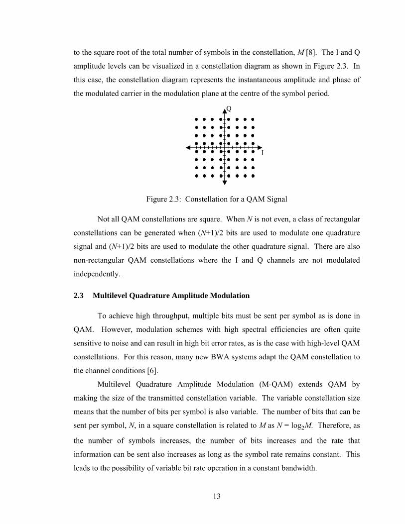
to the square root of the total number of symbols in the constellation, M [8]. The I and Q
amplitude levels can be visualized in a constellation diagram as shown in Figure 2.3. In
this case, the constellation diagram represents the instantaneous amplitude and phase of
the modulated carrier in the modulation plane at the centre of the symbol period.
I
Q
Figure 2.3: Constellation for a QAM Signal
Not all QAM constellations are square. When N is not even, a class of rectangular
constellations can be generated when (N+1)/2 bits are used to modulate one quadrature
signal and (N+1)/2 bits are used to modulate the other quadrature signal. There are also
non-rectangular QAM constellations where the I and Q channels are not modulated
independently.
2.3 Multilevel Quadrature Amplitude Modulation
To achieve high throughput, multiple bits must be sent per symbol as is done in
QAM. However, modulation schemes with high spectral efficiencies are often quite
sensitive to noise and can result in high bit error rates, as is the case with high-level QAM
constellations. For this reason, many new BWA systems adapt the QAM constellation to
the channel conditions [6].
Multilevel Quadrature Amplitude Modulation (M-QAM) extends QAM by
making the size of the transmitted constellation variable. The variable constellation size
means that the number of bits per symbol is also variable. The number of bits that can be
sent per symbol, N, in a square constellation is related to M as N = log2M. Therefore, as
the number of symbols increases, the number of bits increases and the rate that
information can be sent also increases as long as the symbol rate remains constant. This
leads to the possibility of variable bit rate operation in a constant bandwidth.

14
The size of the QAM constellation that can be reliably used is limited by the
tolerable BER at the minimum received SNR and the subsequent PER performance.
Since SNR can vary dramatically due to fading in the wireless channel, it is difficult to
design adequate fade margin into a power-limited link to maintain sufficient SNR for
acceptable PER performance in high-level QAM. Therefore, it is advantageous to adapt
the size of the QAM constellation by sending a variable number of bits per symbol on a
burst-by-burst basis.
M-QAM modems can use any size of constellation but sizes of ...6,4,2;2 =NN
are typically used because they yield square constellations. Also, when N is even, two
N/2 bit words can be used to describe the constellation where one N/2 bit word relates to
the in-phase amplitude of the constellation point and the other N/2 bit word relates to the
quadrature amplitude of the constellation point. The M-QAM transceiver proposed in
this thesis operates with four square QAM constellations: QAM-4, QAM-16, QAM-64
and QAM-256, which are shown in Figure 2.4a, b, c and d respectively.
(b)
Q
I
(d)
Q
I
(c)
Q
I
(a)
Q
I
Figure 2.4: QAM Constellations
The sensitivity of a constellation to additive noise is determined by the distance
between constellation points. The constellations in Figure 2.4 show that, when the
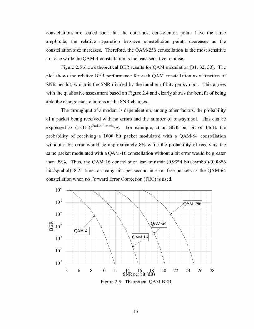
15
constellations are scaled such that the outermost constellation points have the same
amplitude, the relative separation between constellation points decreases as the
constellation size increases. Therefore, the QAM-256 constellation is the most sensitive
to noise while the QAM-4 constellation is the least sensitive to noise.
Figure 2.5 shows theoretical BER results for QAM modulation [31, 32, 33]. The
plot shows the relative BER performance for each QAM constellation as a function of
SNR per bit, which is the SNR divided by the number of bits per symbol. This agrees
with the qualitative assessment based on Figure 2.4 and clearly shows the benefit of being
able the change constellations as the SNR changes.
The throughput of a modem is dependent on, among other factors, the probability
of a packet being received with no errors and the number of bits/symbol. This can be
expressed as (1-BER)Packet Length×N. For example, at an SNR per bit of 14dB, the
probability of receiving a 1000 bit packet modulated with a QAM-64 constellation
without a bit error would be approximately 8% while the probability of receiving the
same packet modulated with a QAM-16 constellation without a bit error would be greater
than 99%. Thus, the QAM-16 constellation can transmit (0.99*4 bits/symbol)/(0.08*6
bits/symbol)=8.25 times as many bits per second in error free packets as the QAM-64
constellation when no Forward Error Correction (FEC) is used.
1E-8
1E-7
1E-6
1E-5
1E-4
1E-3
1E-2
4 6 8 10 12 14 16 18 20 22 24 26 28SNR per bit (dB)
BER
QAM-4QAM-16
QAM-64
QAM-256
10-7
10-8
10-6
10-5
10-4
10-3
10-2
Figure 2.5: Theoretical QAM BER

16
An M-QAM system can only work in a duplex transmission system since the
transmitter needs to know the quality of the link as perceived by the receiver. Since
adaptation is on a burst-by-burst basis, the channel fading must occur slowly compared to
the burst length for the adaptation to be effective. For a TDD system, such as the one
implemented for this thesis, all radios transmit on the same frequency. Therefore,
transmissions between two radios experience similar fading for transmissions in both
directions. Because the channel is similar in both directions, a radio node can use the last
burst received from a particular radio to estimate the channel integrity and determine the
number of QAM levels to be used for transmission between those two radios [9].
Although the adaptation control system and channel estimation are beyond the
scope of this thesis, the channel integrity can be estimated using the received BER. To
determine the BER, FEC is applied to all or part of the transmitted packets so that the
receiver can determine the number of bit errors, up to a maximum determined by the type
of FEC, in the received packets. From the BER of the current and previous received
packets, the appropriate modulation level can be selected to obtain the desired BER for
the next transmission. This method has the disadvantage of being slow since it relies on
statistically significant number of bit errors occurring in order to estimate the channel
integrity.
Alternatively, the channel integrity can be estimated using the received SNR. In
practice, the SNR can be estimated from the average signal level and the Error Vector
Magnitude (EVM), which is the distance from the actual location of the received symbol
to the ideal location of the received symbol in the vector signal space. From the SNR
estimate, the modulation level can be set for the next transmission. To do this, a
constellation can be chosen from the BER curves to achieve a specified BER for the
approximate noise level in the channel. Thus, the modulation level can be selected using
the received signal strength and the EVM.
2.4 Sampling Theory
An analog signal, y(t), can be represented by a sequence of numerical symbols,
y(n), if the rate at which the analog sequence is sampled to generate the numerical
symbols is greater than two times the highest frequency component in the analog signal.

17
Figure 2.6 shows a sinusoidal waveform with a frequency Fw sampled at three
frequencies of Fs=5Fw, Fs=2.1Fw Fs=1.5Fw. The plots on the left side of the figure show
the time domain representation of the waveform while the plots on the right show the
Power Spectral Density (PSD) of the sampled waveform.
PSD
Fs=5Fw
PSD
Fs=2.1Fw
PSD
Fs=1.5Fw
0 0.5 1 1.5 20
1
0 0.5 1 1.5 20
1
0
1
0 π 2π Frequency (Radians/Sample)
0 π 2π Frequency (Radians/Sample)
0 π 2π Frequency (Radians/Sample)
1
.8
.6
.4
.2
0
.2
.4
.6
.8
1
1
8
6
4
2
0
2
4
6
8
1
0 2 4 6 8 10 12 14 16 18 201
.8
.6
.4
.2
0
.2
.4
.6
.8
1
Am
plitu
de
Am
plitu
de
Am
plitu
de
0 5 10 Time (s)
0 5 10 Time (s)
0 5 10 Time (s)
Figure 2.6: Sampled Waveforms
The plots show that the waveforms sampled at a frequency greater than two times
the highest frequency component can be uniquely identified. The signal sampled at five

18
times the signal frequency, Fw, has frequency components at 2π/5 and 2π-2π/5. Similarly,
the signal sampled at 2.1Fw has frequency components at 2π/2.1 and 2π-2π/2.1. The
signals sampled at 5Fw and 2.1Fw appear to be different frequencies in the frequency
domain plots because the plots are normalized by the sampling frequency.
The signal sampled at 1.5 times the signal rate has frequency components at
2π/1.5 and 2π-2π/1.5. However, the frequency components are identical to the frequency
components for a signal at half that frequency (2π/3=2π-2π/1.5 and 2π-2π/3=2π/1.5)
which is shown by the dotted line in the time domain. The phenomenon by which a
given signal appears to be a signal with a different frequency is known as aliasing.
Aliasing occurs when a signal is sampled below the Nyquist rate, which is two times the
highest frequency component of the signal.
2.4.1 Upsampling
Upsampling is a process by which a signal that has been sampled at one rate is
represented at a higher sample rate. When a signal, y(n), is upsampled by an integer
factor of G, the upsampled signal y´(n) is given by Equation 2.6.
⎪⎩
⎪⎨⎧
⎟⎠⎞
⎜⎝⎛
=′ otherwise0
Integeran is )( Gn
Gnyny (2.6)
Figure 2.7 shows a time domain representation of a signal, y1(n), before and after
upsampling by a factor of two.
0 10 20−1
0
1
0 5 10−1
0
1
Am
plitu
de
Am
plitu
de
Time (Samples)(a)
Time (Samples) (b)
y1(n) y1´(n)
Figure 2.7: Time Domain View of Upsampling

19
Upsampling causes the frequency spectrum of a sampled signal to be compressed
in frequency relative to the sampling frequency and replicated. The frequency domain
effect of upsampling by a factor of two is shown in Figure 2.8 where an arbitrary
spectrum Y2(ω) is upsampled by two to give Y2´(ω). Mathematically, the spectral images
generated by upsampling are centred at 2πn/G-π/G where n=1, 2, …, G. PS
D
0 π 2πFrequency (Radians/Sample)
(a) PS
D
0 π 2πFrequency (Radians/Sample)
(b)
Y2(ω) Y2´(ω)
Figure 2.8: Frequency Domain View of Upsampling
Although upsampling results in compression of the spectrum relative to the
sample rate by a factor of G, the sample rate is increased by a factor of G when
upsampling. Therefore, the width of the new spectrum in Hz is multiplied by G and the
new spectrum contains the original G copies of the original spectrum, each of which has
the same width as the original spectrum.
2.4.2 Downsampling
Downsampling is a process by which a signal that has been sampled at one rate is
represented at a lower sample rate. When a signal, y(n), is downsampled by an integer
factor of G, the downsampled signal y´(n) is given by Equation 2.7.
( )nGyny =′ )( (2.7)
Figure 2.9 shows a time domain representation of a signal before and after downsampling
by a factor of two.
Downsampling causes the frequency spectrum of a sampled signal to be divided
into G equally sized segments that are added together and then expanded in frequency

20
0 5 10−1
0
1
0 10 20−1
0
1
Am
plitu
de
Am
plitu
de
Time (Samples)(a)
Time (Samples) (b)
y3(n) y3´(n)
Figure 2.9: Time Domain View of Downsampling
relative to the sampling frequency. Mathematically, the operation can be described as
∑−
=⎟⎠⎞
⎜⎝⎛ −
=′1
0
2)(G
i GiYY πωω (2.8)
where ω is the frequency in Radians/Sample, Y is the frequency spectrum of the original
signal, and Y΄ is the frequency spectrum of the downsampled signal.
Downsampling results in expansion of the summed spectral segments relative to
the sample rate by a factor of G resulting in a spectrum that still reaches from 0 to 2π
radians/sample. However, the sample rate is decreased by a factor of G when
downsampling. Therefore, the width of the new spectrum in Hz is 1/G times the width of
the original spectrum.
The frequency domain effect of downsampling by a factor of two is shown in
Figure 2.10. In the case of the spectrum shown in Figure 2.10a, different parts of the
original spectrum overlap in the new spectrum and add.
PSD
0 π 2πFrequency (Radians/Sample)
(a)
PSD
0 π 2πFrequency (Radians/Sample)
(b)
Y4(ω) Y4´(ω)
Figure 2.10: Frequency Domain View of Downsampling

21
2.4.3 Undersampling
For bandpass signals, the signal does not necessarily have to be sampled at twice
the frequency of the highest frequency component. Shannon’s Information Theorem
states that the signal can be sampled at a rate that is twice the bandwidth of the signal
without losing information. This will cause the sampled signal to appear as an alias of
the original bandpass signal. However, all of the information in the bandpass signal will
be present in the sampled representation of the signal.
Figure 2.11 illustrates how the bandpass signal is aliased at frequencies above and
below its actual frequency when sampled at a rate, Fs, lower than the signal frequency. If
the sampling frequency is chosen correctly, any signal can be undersampled such that the
sampled signal is centred at π/2 radians/sample. To centre the undersampled signal at π/2
radians/sample, the centre frequency of the original signal in Hz, FBP, and the
sampling frequency in samples per second must be related by
⎟⎠⎞
⎜⎝⎛ ±=
41nFF sBP (2.9)
where n is a positive integer.
PSD
0 Fs 2 Fs 3FsFrequency (Hz)
Original Spectrum
Aliased Copies of Original Spectrum
Aliased Copy of Original Spectrum
Figure 2.11: Frequency Domain View of Undersampling
2.5 Digital to Analog Conversion
The power spectrum output by a Digital to Analog (D/A) converter depends on
the data sequence sent to the D/A converter and the shape of the electrical waveform
generated by the D/A converter. D/A converters generally produce rectangular pulses
with the pulse amplitude determined by the data words received and a width equal to the
time between data words, Ts, as shown in Figure 2.12.

22
Am
plitu
de
0 5 10Samples
(a)
Am
plitu
de
0 5 10Time (s)
(b)
Digital Sequence Analog Waveform
Figure 2.12: D/A Output
Mathematically, the D/A conversion process can be viewed as the time-domain
convolution of the sampled sequence with a rectangular function that has unit amplitude
from time t=0 to time t=Ts and an amplitude of zero everywhere else. Therefore, in the
frequency domain, the D/A conversion process can be viewed as the multiplication of the
spectrum of the sampled signal (and its aliases) with the spectrum of the rectangular
pulse.
The square shape of the D/A converter pulses causes the PSD to be shaped by
2
2sin
⎟⎟⎠
⎞⎜⎜⎝
⎛
⎟⎟⎠
⎞⎜⎜⎝
⎛
⋅
s
ss
Ff
Ff
kπ
π
(2.10)
where ks is a constant determined by the D/A converter. However, the distortion
introduced by the D/A converter can be removed by changing the response of the
reconstruction filter or by inserting a digital filter before the D/A to pre-distort the signal
so that the output of the D/A converter is spectrally flat over the desired frequency range.
Section 7.4.2 describes how a digital filter can be used to compensate for the distortion
introduced by the D/A converter.
Figure 2.13a shows the spectrum of a digital signal and Figure 2.13b shows the
spectrum of the same signal after digital to analog conversion from zero to three times Fs.
The plots show two important characteristics of D/A conversion: spectral shaping from
the square shape of the D/A converter pulses (shown by the dotted line) and the presence
of aliases of the original signal.

23
0 1 2 3−40
−20
0
−40
−20
0
PSD
(dB
)
PSD
(dB
)
0 0.5 1 Frequency (*Fs Hz)
(a)
Frequency (*Fs Hz)
(b) Figure 2.13: D/A Effects
An analog filter is usually used to limit the bandwidth of the analog signal. This
filter is known as a reconstruction filter because it “reconstructs” the analog signal that
the sampled waveform was generated from. The reconstruction filter suppresses all but
one of the spectral images present. Figure 2.14 shows four frequency spectra that
0 1 2 3−40
−20
0
0 1 2 3−40
−20
0
PSD
(dB
)
PSD
(dB
)
Frequency (*Fs Hz)
(a)
Frequency (*Fs Hz)
(b)
0 1 2 3−40
−20
0
0 1 2 3−40
−20
0
Frequency (*Fs Hz)
(c)
Frequency (*Fs Hz)
(d)
PSD
(dB
)
PSD
(dB
)
Figure 2.14: Reconstruction Filtering

24
illustrate reconstruction filtering. The dotted line in Figure 2.14a shows a low-pass
reconstruction filter and Figure 2.14b shows the resulting spectrum. The dotted line in
Figure 2.14c shows a band-pass reconstruction filter and Figure 2.14d shows the resulting
spectrum. The use of a pass-band reconstruction filter is useful because it can provide
upconversion of the signal to the IF frequency used by the radio.
2.6 Digital QAM Transmitter
The structure of a typical digital QAM transmitter implemented in digital logic is
shown in Figure 2.15. The transmitter consists of two branches: one for the In-phase (I)
channel and one for the Quadrature (Q) channel. The operation of the transmitter can be
understood by tracing the flow of data through the functional blocks inside the
transmitter.
Quadrature Modulator
Serial Data
Gray to BinaryEncoder
Serial to Parallel
Gray to Binary Encoder
Symbol Mapper
Symbol Mapper
RRC Filter
RRC Filter
D/A
Modulated Signal
I Q
Figure 2.15: Digital QAM Transmitter
The Serial to Parallel block converts incoming serial data into two N/2 bit words
per symbol. Hence, the symbol rate, Rs, is 1/N times the bit rate, Rb. One N/2 bit word is
then sent to each Gray to Binary Encoder block at the symbol rate.
The words sent to the I channel and Q channel Gray to Binary Encoder blocks can
be thought of as Gray coded numbers that enumerate the I channel and Q channel
locations for each constellation point. Figure 2.16 shows how two bit Gray coded
numbers can be used to enumerate the I and Q channel locations of the points in a
QAM-16 constellation. Gray coded numbers are desirable because the most common

25
Q
I 00
00
01
01
11
11
10
10
Figure 2.16: Gray Coding
type of error occurs when a symbol is detected as an adjacent symbol. In this case, Gray
coded numbers result in only one bit error while binary encoded numbers may result in
multiple bit errors. However, since most digital subsystems operate on binary numbers,
the Gray to Binary Encoder blocks are used to convert the Gray coded number to binary
coded numbers.
The Symbol Mapper blocks convert the binary coded results from the Gray to
Binary Encoder blocks into binary coded transmit levels using Equation 2.11
( )122 2 −−= Nio mm (2.11)
where mo is the mapped value and mi is the input to the Mapper.
If the levels generated by the symbol mappers are used to generate square pulses,
the power of the signal will be spread across a very large bandwidth. Therefore, the
mapped values are filtered by RRC filters to limit the bandwidth of the transmitted signal
without introducing Inter-Symbol Interference (ISI) as described in Chapter 7.
The filtered signals are used to modulate quadrature carriers in the Quadrature
Modulator block. The operation of a quadrature modulator was described in Equation
2.5. The modulated signal is then converted from digital words to an analog signal. The
theory of the digital to analog conversion is described in Section 2.5.

26
2.7 Digital QAM Receiver
The structure of a typical digital QAM receiver implemented in digital logic is
shown in Figure 2.17. The operation of the receiver can be understood by tracing the
flow of data through the functional blocks inside the receiver.
Modulated Signal
Binary to GrayDecoder
Binary to Gray Decoder
Carrier Recovery
RRC Filter
RRC Filter
Serial Data
A/D
Parallel to Serial
Analog
AGC
I Q
Quadrature Demodulator
Symbol Demapper
Symbol Demapper
Clock Recovery
x(t) y(t)
Figure 2.17: Digital QAM Receiver
The AGC block scales the received signal so that the receiver can operate on
signals of constant amplitude. This is particularly important in radio channels where the
attenuation of the channel can vary with time. A detailed discussion of AGC theory is
provided in Chapter 4.
The Analog to Digital (A/D) converter samples the received signal when triggered
by the clock recovery subsystem. The clock recovery subsystem triggers the A/D
converter a fixed number of times per symbol. The number of samples per symbols is
determined by the structure of the RRC filters. Furthermore, the samples are equally
spaced with one of the samples ideally occurring in exactly the centre of the symbol
period. Chapter 5 provides a detailed description of the need for symbol timing recovery
and symbol timing recovery theory.

27
The Quadrature Demodulator block demodulates the received signal, s(t), to
obtain AI´ (t) and AQ´ (t), which are approximations of AI(t) and AQ(t). Demodulation is a
two-step process that consists of multiplying the received signal by sine and cosine
waveforms that are phase coherent with the received signal and then low-pass filtering
the results as shown in Equations 2.12 to 2.21, where LPF· denotes the low-pass
filtering operation.
)2cos(2)(LPF)( tftstA cI π×=′ (2.12)
[ ] )2cos(2)2sin()()2cos()(LPF)( tftftAtftAtA ccQcII πππ ×−=′ (2.13)
[ ] [ ] )4sin()()4cos(1)(LPF)( tftAtftAtA cQcII ππ −+=′ (2.14)
)4sin()()4cos()()(LPF)( tftAtftAtAtA cQcIII ππ −+=′ (2.15)
)()( tAtA II =′ (2.16)
[ ] )2sin(2)(LPF)( tftstA cQ π−×=′ (2.17)
[ ] [ ] )2sin(2)2sin()()2cos()(LPF)( tftftAtftAtA ccQcIQ πππ −×−=′ (2.18)
[ ] [ ] )4cos(1)()4sin()(LPF)( tftAtftAtA cQcIQ ππ −+−=′ (2.19)
)4cos()()()4sin()(LPF)( tftAtAtftAtA cQQcIQ ππ −+−=′ (2.20)
)()( tAtA QQ =′ (2.21)
The coherent sine and cosine waveforms used by the quadrature demodulator are
generated by the carrier recovery subsystem. Chapter 6 describes the effects of
demodulation by signals that are not phase coherent with the carrier of the received signal
and the theory of carrier recovery.
The RRC Filter blocks filter the outputs of the Quadrature Demodulator to
remove noise, interference, and ISI. Following filtering, the Symbol Demappers, Gray
Decoders and Parallel to Serial blocks reverse the operations of the Symbol Mappers,
Gray Coders and Serial to Parallel blocks in the transmitter. A detailed discussion of
filter theory and its application to communications systems is presented in Chapter 7.

28
Chapter 3
M-QAM Transceiver Architecture
3.1 Overview
An objective of this thesis is to design and evaluate a burst-mode M-QAM
architecture. To do this, three architectural principles will be used:
• the modem should support variable bit rate operation while operating at a constant
symbol rate,
• the modem should minimize redundant hardware required to operate on multiple
constellations, and
• the synchronization loops should operate quickly to synchronize with received bursts
while tracking the burst through the data segment without knowing the size of the
constellation.
Buffering in the transmitter is proposed to allow a fixed bit rate packet input to the
transmitter to support variable channel bit rate operation. Similarly, buffering in the
receiver is proposed to allow a fixed bit rate packet output from the receiver to support
variable channel bit rate operation. Support for variable bit rate operation is required
because the instantaneous bit rate in the channel, Rb, is related to the fixed symbol rate in
the radio channel, Rs, by Rb = NRs. Thus, changing the number of bits per symbol, N, in
response to changing channel conditions causes a corresponding change in Rb. Further,
since the inputs and outputs of the system are based on packet transmission, it is suitable
for use with systems carrying variable rate packetized data such as Internet Protocol (IP)
packets.
To minimize redundant hardware, a bit stuffing and shifting architecture was
proposed by Aspel and Klymyshyn [34] that operates with variable word and

29
constellation sizes without requiring separate hardware for each. The proposed M-QAM
architecture modifies the transmitter to perform a stuffing operation to pad the variable
bit length words needed for M-QAM to a fixed word size. The transmitter also performs
a shifting operation to remove Direct Current (DC) offsets generated by the mapping of
the padded words into the transmit waveforms. The receiver is modified in a similar
manner to remove the shifting and padding introduced in the transmitter.
Amplitude detection, symbol clock recovery, and carrier recovery are proposed
that operate on multiple constellations during the data segment of received bursts without
knowing the constellation size. These functions use specific preamble sequences to
simplify the hardware requirements for each of these functions by generating initial
estimates from the simple preamble sequences. The functions are not independent and
operate simultaneously to achieve burst synchronization.
3.2 System Architecture
The M-QAM system is designed to operate at one mega-symbol per second while
transmitting either 2, 4, 6, or 8 bits per symbol. The baseband QAM signal is digitally
upconverted to 3 MHz by the IF Filtering block and then converted to an analog signal.
Digitally filtering the QAM signal eases the requirements on the reconstruction filter and
the anti-aliasing filter. The modem would require further upconversion to the desired
operating frequency for real-world use; however, the actual channel will be simulated at
3 MHz.
Baseband M-QAM Transmitter
Reconstruction Filter
D/A
Channel
Digital IF Filtering
Baseband M-QAM Receiver
Anti-aliasing Filter
A/D Digital IF Filtering
Transmitter
Receiver Figure 3.1: System Architecture

30
The system is comprised of a transmitter and a receiver as shown in Figure 3.1.
The transmitter consists of a baseband M-QAM transmitter, digital IF filtering, digital to
analog conversion, analog filtering, and amplification. The receiver consists of an
amplifier, an anti-aliasing filter, analog to digital conversion, digital IF filtering, and a
baseband M-QAM receiver.
3.3 Burst-Mode M-QAM Transmitter
The proposed design for the digital burst-mode M-QAM transmitter is shown in
Figure 3.2. The M-QAM transmitter is similar to the QAM transmitter shown in Figure
2.15 except for the replacement of the Serial to Parallel block with the Packet Generator
block, the addition of a Digital IF Filtering block, and modifications to the Symbol
Mapper blocks.
In the M-QAM transmitter, the number of symbols in the constellation, ,M and
the number of bits per symbol, ,N are variable on a burst-by-burst basis. This results in a
channel bit rate that is different for each M. However, the input to the transmitter is
based on a fixed bit rate packet link. The Packet Generator block shown in Figure 3.2
buffers incoming data for each packet so that the channel bit rate is easily changed for
different constellations.
Quadrature Modulator
Serial Data
Gray to Binary Encoder
Packet Generator
Gray to Binary Encoder
Modified SymbolMapper
Modified Symbol Mapper
RRC Filter
RRC Filter
Digital IF Filtering
D/A
Modulated Signal
I Q
Figure 3.2: Burst-Mode M-QAM Transmitter

31
The Digital IF Filtering block was added to reduce the filtering requirements
imposed on the reconstruction filter. The IF Filter block upsamples the modulated signal
and then filters away all but one of the spectral images. This allows a simpler analog
filter to be used as a reconstruction filter since the used spectrum and aliased spectral
images generated by the D/A converter will be farther apart in the frequency domain.
Two other critical modifications are necessary in the M-QAM transmitter. The
input words are stuffed in a specific manner before Gray to binary conversion so that the
transmitter is able to operate on words of a fixed size. The Symbol Mapper blocks
perform a shifting operation after the normal mapping operation in the transmitter to
remove DC offsets generated by the mapping of the padded words into the transmit
waveforms.
3.4 Burst-Mode M-QAM Receiver
The proposed design for the M-QAM receiver is shown in Figure 3.3. The M-
QAM receiver is similar to the QAM receiver shown in Figure 2.17; however, there are a
number of notable changes. The changes include modifications to the AGC and carrier
recovery subsystems, added filtering, and modifications to the Symbol Demapper blocks
to support multiple constellations. Furthermore, the control signals from the AGC,
Carrier Recovery, and Amplitude Detection blocks are shown as dashed lines to
distinguish them from the data path shown by solid lines.
The analog AGC has been removed and a digital AGC has been implemented by
the Amplitude Detection and Scaler blocks. The analog AGC was omitted from the
modem to limit the scope of the project. However, a digital AGC with a limited dynamic
range is added to provide a quick responding AGC for the receiver. The digital AGC
could be extended to a full analog AGC if it were extended to control an external
attenuator or amplifier.
The carrier recovery function is implemented as a feedback loop within the
Carrier Recovery and Derotator blocks. The Carrier Recovery block, using the filtered I
and Q channel symbols, acts as the phase detector and loop filter while the Derotator
corrects the phase. Both blocks are located after the RRC filters in order to reduce the
delay around the feedback loop.

32
An IF Filter block has been added to reduce the filtering requirements of the anti-
aliasing filter. The IF Filter block filters away noise and adjacent channel interference
and then downsamples the data stream. This allows a simpler analog filter to be used as
an anti-aliasing filter since the IF filter will suppress noise and interference admitted by
the anti-aliasing filter.
Modulated Signal
IF Filter
Derotator
RRC Filter
RRC Filter
Serial Data
Scaler
Scaler
Packet Buffer
Carrier Recovery
AmplitudeDetection
A/D
I Q
Quadrature Demodulator
Modified SymbolDemapper
Modified Symbol Demapper
Clock Recovery
Binary to Gray Decoder
Binary to Gray Decoder
Figure 3.3: Burst-Mode M-QAM Receiver
In the M-QAM receiver, the number of bits per symbol, N is variable on a burst-
by-burst basis. This results in a channel bit rate that is potentially different for each burst.
However, rate conversion is handled by buffering in the Packet Buffer block shown in
Figure 3.3 that replaces the simple Parallel to Serial converter in the standard QAM
receiver shown in Figure 2.17.

33
Two critical modifications in the M-QAM receiver parallel changes in the
M-QAM transmitter. First, the Symbol Mapper blocks perform a shifting operation after
the normal demapping operation in the transmitter to reintroduce the DC offset removed
in the transmitter. Second, the input words are unstuffed after Gray coding to recover the
transmitted data.
3.5 Bit Stuffing and Shifting
To obtain an efficient hardware implementation, redundant hardware is avoided.
Normally, each constellation would require separate hardware to be received and
demodulated; however, a bit stuffing and shifting architecture is implemented that uses
one set of hardware for all constellations. This bit stuffing and shifting architecture not
only allows one set of hardware to receive multiple constellations, it also allows the
synchronization functions to operate independently of the received constellation.
The proposed M-QAM architecture modifies the transmitter to perform a
stuffing operation to pad the N bit words to a fixed size. The transmitter also performs a
shifting operation to remove DC offsets generated by the mapping of the padded words
into the transmit waveforms. The receiver is modified in a similar manner to remove the
shifts and padding introduced in the transmitter.
3.5.1 Packet Generator
The M-QAM modem architecture operates in burst mode. The Packet Generator,
shown in Figure 3.2, buffers incoming data until a burst of data is sent by the modem.
From the buffered data, the Packet Generator creates input words consisting of N bits
where N is even and ranges from a minimum size of 2 to a maximum size, Nmax, of 8.
Each N bit word contains two N/2 bit words: one for the I channel and one for the Q
channel. The added benefit is that the variable bit rate operation inherent in M-QAM is
easily facilitated by the buffering capability of the packet generator.
The packet buffer also inserts a specific preamble sequence at the beginning of
each burst. This preamble consists of a repeating QAM-4 sequence that the
synchronization functions use to detect an incoming burst and to generate initial estimates
for the automatic gain control, carrier recovery, and symbol timing recovery loops.

34
Using the initial estimates, the synchronization functions can operate on multiple
constellations during the data segment of the burst without knowing which constellation
is being received.
3.5.2 Gray Coding and Bit Stuffing
The conversions from Gray code to binary and binary to Gray code are based on a
fixed word size. However, for M-QAM, the Gray to Binary Encoder needs to support
input word sizes ranging from 1 to Nmax/2, where Nmax is the word length for the largest
constellation supported. Variable sizes can be accommodated if the input words are
stuffed to obtain a fixed word size. The Gray to Binary Encoder stuffs the N/2 bit words
to create an input word consisting of Nmax/2 bits before conversion. The Binary to Gray
Decoder performs the reverse operation in the receiver after conversion.
The stuffing process is shown in Figure 3.4 for each Gray to Binary Encoder. The
N/2 least significant bits of each Nmax/2 bit word are used for data while the Nmax/2- N/2
most significant bits are stuffed with zeros. With this word format, Gray coding or
decoding results in words with the Nmax/2- N/2 most significant bits containing zeros.
This format is important because it allows the use of a standard mapping algorithm that
maps N/2 bits into 2N/2 levels.
a) N/2 Bit Word
b) Nmax/2 Bit Word
c) Nmax/2 Bit Word
D D
0 D D
Stuffing
0 D´ D´
Gray to Binary Encoding
Figure 3.4: Bit Stuffing and Gray Coding/Decoding for QAM-16 (N/2=2, Nmax/2=3)

35
3.5.3 Mapping and Shifting
The mapping operation transforms the unsigned binary Nmax/2 bit words into
signed, DC balanced values ranging from )12( 2 −− maxN to 12 2 −maxN . Fixed
constellation QAM systems use the standard mapping operation shown in Equation 2.11.
The standard mapping operation cannot be directly used in an M-QAM system
because only the 2N least significant bits of a 2maxN bit input word contain data.
These input words represent numeric values contained in the range 0 to 12 2 −N . The
transmit levels that result from mapping inputs of 0 to 12 2 −N are unbalanced, as shown
in Figure 3.5, and include the lowest 22 N levels out of the possible 22 maxN levels.
Balanced levels, also shown in Figure 3.5, are obtained by shifting the levels as
⎟⎠⎞⎜
⎝⎛ −+= 2/2/
22 NaxmNoob mm (3.1)
where mob is the balanced level and mo is the unbalanced output of the standard mapping
operation.
7
3
6 5 4
2 1 0
7
-1
5 3 1
-3 -5 -7
Mapper Input Balanced
7
-1
5 3 1
-3 -5 -7
Unbalanced Figure 3.5: Mapper Input and Mapped Levels for QAM-16 (N/2=2, Nmax/2=3)
The Demapper in the receiver is constructed in a similar manner. First, the
balanced I and Q signals are converted into unbalanced signals using Equation 3.1 to
obtain mo given mob. Then the standard demapping operation is performed using
Equation 2.11 to obtain the unsigned binary coded word, mi, given mo. Thus, after the
Demapper, an 2maxN bit word with data in only the 2N least significant bits and zeros
in the 22 NNmax − most significant bits is obtained for each of the I and Q channels.

36
3.6 Burst Format
The burst format consists of a preamble followed by a data segment as shown in
Figure 3.6. In turn, the preamble consists of a synchronization sequence followed by
information about the burst. The symbols in the preamble are chosen from four
constellation points. The points are chosen such that the preamble can be demodulated as
a QAM-4 constellation whether the constellation is actually QAM-4, QAM-16, QAM-64,
or QAM-256. Two examples of possible preamble point selections are shown in Figure
3.7.
The choice of preamble points greatly affects the complexity and the performance
of the receiver. Choosing points that form a QAM-4 constellation simplifies the receiver
design but the choice of which four constellation points can still have a significant impact
on implementation complexity of the AGC subsystem. The choice of which four
constellation points to use is described in Chapter 4.
Payload Packet
InfoSync Sequence
Data Segment Preamble
QAM-4 M-QAM
Figure 3.6: Burst Format
(a) (b)
Q
I
Q
I
Figure 3.7: Preamble Point Selections for QAM-64

37
3.7 Detecting the Burst
The synchronization sequence is a standard preamble pattern that consists of a
repeating sequence of ),( aa − , ),( aa− terminated by ),( aa where the first element in the
coordinate is the I channel amplitude, the second element in each coordinate is the Q
channel amplitude and a is a constant [21].
The burst is found by detecting a “sync word” that can be all or part of the
synchronization sequence. A sync word is detected using a frame synchronizer as shown
in Figure 3.8. The frame synchronizer outputs a binary 1 when the data in the shift
register equals the sync word, (S1, S2, S3… SLsync) where Lsync is the length of the sync
word.
…
Shift Register
S2 S1 S3 SLsync
.
.
.
Clock
Data
Frame Sync
Figure 3.8: Frame Synchronizer
The length of the sync word governs both the probability that the frame
synchronizer will falsely detect the synchronization sequence and the probability that the
frame synchronizer will fail to detect the synchronization sequence. The probability that
a false synchronization at any given symbol, Pfs, will occur is given by

38
syncsync L
L
fsP −=⎟⎠⎞
⎜⎝⎛= 2
21 (3.2)
where Lsync is the length of the sync word [8]. The lower bound for the probability of not
synchronizing with a burst, Pns, is defined by the probability of a bit error and is given by
esyncns PLP ×= (3.3)
where Pe is the probability of a bit error for the synchronization sequence.
3.8 Detecting the Data Segment
The M-QAM modem is designed to operate with variable length synchronization
sequences. This allows the other synchronization functions more symbols to generate
estimates before the data segment starts if required. This is useful because a QAM-256
constellation requires more accurate symbol timing and carrier estimates than a QAM-4
constellation requires.
The end of the synchronization sequence is detected by the presence of a ),( aa
symbol. The data segment starts a fixed number of symbols after the synchronization
sequence because the packet information at the end of the preamble is composed of a
fixed number of symbols.
3.9 Modulation Level
The unstuffing operation that is performed in the receiver needs to know N, the
number bits per symbol, or the modulation level, M, since M=2N. N can be inferred from
the decoded data, encoded into the synchronization sequence, or encoded into the packet
information section of the preamble.
If the receiver relies on the demodulated data to infer the number of bits per
symbol, the receiver must buffer data words and cannot begin unstuffing the data words
until a considerable number have been received. The technique used to infer N from the
demodulated data relies on the fact that the most significant Nmax/2-N/2 bits of each
received word will be filled with zeros using the stuffing technique described in
Section 3.5.2. However, this technique is susceptible to errors due to a sequence of
symbols that result in zeros occurring in the most significant bits by chance. The chance

39
of error due to zeros occurring in the most significant bits by chance in random data is
inversely proportional to the number of symbols used to infer N.
The number of bits per symbol can be encoded into the synchronization sequence
by varying the amplitudes of the symbols in the sequence. An example of a multilevel
synchronization sequence is (-a, +a), (+a, -a), (-1, +1), (+1, -1)… where a=2N/2-1. This
code gives information about N in the ratio of symbol amplitudes and provides an
average amplitude of N/2 times the bin size. However, this type of a synchronization
sequence increases the complexity of other synchronization functions due to increased
jitter in the zero crossings for the symbol timing recovery circuit and jitter in the symbol
amplitudes for the automatic gain control.
The implemented M-QAM system encodes the number of bits per symbol, N, into
the packet information section of the preamble. N is encoded by the sign of the I and Q
channel components of a single symbol, (b, c) where |b| = |c| = a. N is calculated by
N = 4(b>0)+2(c>0)+2. An important concern for this technique is redundancy and error
tolerance because incorrect determination of the end of the preamble or the constellation
size will result in corruption of an entire burst. To reduce the chances of losing an entire
burst in future versions of the modem, forward error correction can be incorporated into
the preamble to reduce the likelihood of incorrect determination of N.
3.10 Burst Length
The receiver must be able to determine the length of the burst. This information
could be inferred from the received data, encoded into the packet information section of
the preamble, or the receiver could use a fixed burst length. Inferring the length of the
burst from the data is possible for many payloads but it is not possible to infer the length
from random data that was used for testing so this method was not used. The burst length
could easily be encoded into the packet information section of the preamble using a
binary number to represent the length of the burst, however, the robustness of this
technique is limited unless forward error correction is used. The implemented M-QAM
system uses a fixed burst length. This option represents the simplest implementation and
provides an easy transition to encoding the burst length in the preamble if variable length
bursts are required.

40
Chapter 4
Automatic Gain Control
4.1 Overview
The amplitude of received signals can vary dramatically as a function of time in a
wireless channel. Automatic Gain Control (AGC) is used to normalize the amplitude of
the received signal. Both feed-forward and feedback techniques have been developed to
correct amplitude variation. The most popular techniques use average signal power or
average signal amplitude to set the gain of an analog amplifier and possibly coefficients
for a digital multiplier to normalize the received signal.
For the M-QAM system developed for this thesis, the AGC analysis will focus on
using a digital multiplier to normalize the received signal. The analysis assumes that an
analog AGC roughly normalizes the received signal at the beginning of each received
burst. The digital AGC will then fine-tune the amplitude normalization and track
changes in the amplitude of the received signal throughout the burst.
To simplify the hardware in the receiver, the AGC is designed such that the scaled
I and Q signals in the receiver have the same bin size for every M. For a two-dimensional
constellation such as QAM where the constellation points are equally spaced, bin size is
equal to the maximum amplitude in a dimension for which a symbol will be judged to
match a given constellation point minus the minimum amplitude in a dimension for
which a symbol will be judged to match the same constellation point. For the QAM-16
constellation in Figure 4.1, the bin size would be 2.0 units since the decision lines are 2.0
units apart.

41
1 2 3-1 -2 -3
1
2
3
-1
-2
-3 2
2
Figure 4.1: Bin Size
4.2 Effect of Amplitude Variation
For a PAM or a QAM signal, small changes in amplitude can result in symbol
errors. Figure 4.2 shows three versions of a scaled PAM constellation. Dotted lines
7
-1
531
-3-5-7
1513119
-9 -11 -13-15
1.0x0.9x 1.1x
(b)(a) (c)
Figure 4.2: Scaled PAM Constellations

42
show the decision points between bins. Figure 4.2b shows constellation points that are in
the centre of their respective bins; that is, midway between the dotted decision lines that
delineate the bins for each constellation point. Figure 4.2a shows the same constellation
scaled to 90% of its original size and Figure 4.2c shows the same constellation scaled to
110% of its original size. In both cases, scaling the constellation by 10% causes bit errors
by moving some of the constellation points across decision lines.
4.3 Burst Mode AGC
The AGC must rapidly and reliably normalize the amplitude of each received
burst. Rapid normalization of the received signal is aided by the use of a preamble with
symbols that are all the same amplitude as described in Sections 3.6 and 3.7. This allows
gain for the receiver to be calculated quickly without requiring frame synchronization or
a long-term average from random data.
Some AGC systems track amplitude of the received signal throughout the
received burst while others use only a gain setting calculated from the preamble. If the
amplitude is not tracked throughout the burst, the BER will degrade as the receive
amplitude changes throughout the burst. If the amplitude is tracked throughout the data
segment, the BER can be maintained over long bursts. However, complexity of the AGC
system is usually increased because different techniques are often used when either the
amplitudes of the received points vary from symbol to symbol or the sequence of symbol
amplitudes is not known. The M-QAM modem implemented for this thesis uses an AGC
system that avoids extra complexity by extending the AGC techniques used on a constant
amplitude preamble to function throughout the data segment where the symbol
amplitudes are not known.
4.4 Feed-Forward AGC vs. Feedback AGC
Feed-forward AGC systems use a number of received symbols to calculate a gain
value that is then used to scale the received points. For Burst-mode systems, the
operation to calculate the gain can be performed once per burst using all or part of the
preamble. The calculated gain is then used throughout the entire burst. Alternatively, the

43
gain can be calculated repeatedly based on a running average using the system shown in
Figure 4.3.
Scaled Symbol
S1
+ -
Target Amplitude Gain
…
Shift Register
S2
S3
SG
1/X
Received Symbol
1/G
Register
+
Figure 4.3: Feed-Forward AGC
Feedback AGC systems use a tracking loop that uses the scaled values to calculate
an updated gain value. Feedback systems typically calculate a new gain setting every
symbol. The operation of a feedback AGC system is shown in Figure 4.4.
Scaled Symbol
Target Amplitude
Gain 1/X
Received Symbol
Loop Filter
Figure 4.4: Feedback AGC

44
4.5 Feedback AGC Implementation
The AGC system implemented for this thesis is a feedback system. The feedback
loop for the M-QAM receiver is implemented by the Amplitude Detection block and the
Scaler blocks shown in Figure 3.3. The Scaler blocks multiply both the I and Q channel
symbols by the gain value generated by the Amplitude Detection block. The Amplitude
Detection block calculates the gain value as shown in Figure 4.5. First, the bin size is
calculated as described in Section 4.5.1 and Section 4.5.2. The bin size is then filtered by
a first order low-pass filter with a gain of 1.0 at 0 Hz, inverted, and scaled by a factor
equal to the fixed bin size used by the receiver. The previous Gain is then multiplied by
this value, stored in a register, and sent to the Scalers.
Bin Size
Scaled QChannel Symbol
Gain
1/X
AmplitudeDetection
Register
Bin Size Calculation
Scaled I Channel Symbol
LPF
I Channel Symbol
Q ChannelSymbol
Q Channel
Scaler
I Channel Scaler
Figure 4.5: Amplitude Detection Block
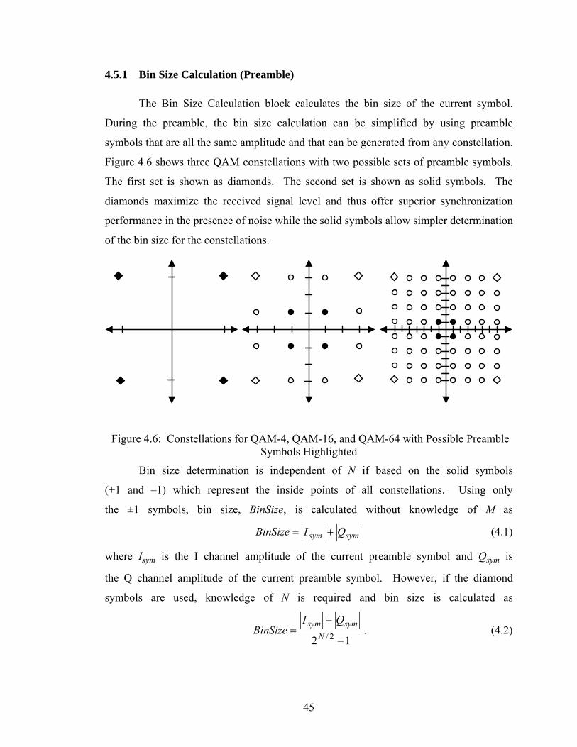
45
4.5.1 Bin Size Calculation (Preamble)
The Bin Size Calculation block calculates the bin size of the current symbol.
During the preamble, the bin size calculation can be simplified by using preamble
symbols that are all the same amplitude and that can be generated from any constellation.
Figure 4.6 shows three QAM constellations with two possible sets of preamble symbols.
The first set is shown as diamonds. The second set is shown as solid symbols. The
diamonds maximize the received signal level and thus offer superior synchronization
performance in the presence of noise while the solid symbols allow simpler determination
of the bin size for the constellations.
Figure 4.6: Constellations for QAM-4, QAM-16, and QAM-64 with Possible Preamble Symbols Highlighted
Bin size determination is independent of N if based on the solid symbols
(+1 and –1) which represent the inside points of all constellations. Using only
the ±1 symbols, bin size, BinSize, is calculated without knowledge of M as
symsym QIBinSize += (4.1)
where Isym is the I channel amplitude of the current preamble symbol and Qsym is
the Q channel amplitude of the current preamble symbol. However, if the diamond
symbols are used, knowledge of N is required and bin size is calculated as
12 2/ −
+= N
symsym QIBinSize . (4.2)

46
From Equation 4.1 and Equation 4.2, it can be seen that, while the diamond
symbols provide better performance, they require both an extra division and N to be
known before the feedback loop can be activated. However, the requirement to know N
before the feedback loop is activated can be modified to a requirement to know N before
the data segment because the received signal does not need to be normalized until the
data segment begins. Thus, Equation 4.1 can be used during the preamble and then the
gain can be adjusted by a factor of 12 2/ −N at the beginning of the data segment to
reflect the actual constellation.
Treating the four diamond shaped preamble points as the solid preamble points
for mathematical convenience has a drawback due to the finite word length in the
modem: the words representing the I channel and Q channel amplitudes will be divided
by 12 2/ −N . This can result in carrier and symbol timing estimates that are not accurate
enough for high order QAM constellations. Therefore, the gain value output by the
Amplitude Detection block is increased by a factor of 15 during the preamble and then
multiplied by ( ) 1512 2/ −N instead of 12 2/ −N at the preamble.
4.5.2 Bin Size Calculation (Random M-QAM Data)
During the data segment, the AGC cannot operate with either of the bin size
calculations described in Section 4.5.1 since the symbols do not have a constant
amplitude for values of M≥4. However, the AGC is extended to operate during the data
segment of the burst by changing the bin size calculation to use the location of the
received point relative to the most likely symbol point.
The process by which the bin size is calculated is shown in Figure 4.7. Figure
4.7a shows one M-QAM symbol. First, the absolute values of the I and the Q channels
are taken. Figure 4.7b shows the symbol after the absolute values have been taken.
Secondly, a modulus operation is applied to both the I and Q channel amplitudes to leave
a “new” symbol at the (+1, +1) location that can be used in the bin size calculations
described in the last section. The modulus operations effectively translate the point down
by the amplitude of the most likely symbol point minus the amplitude of the (+1, +1)
symbol in both the I and Q channels. Figure 4.7c shows the symbol after the modulus
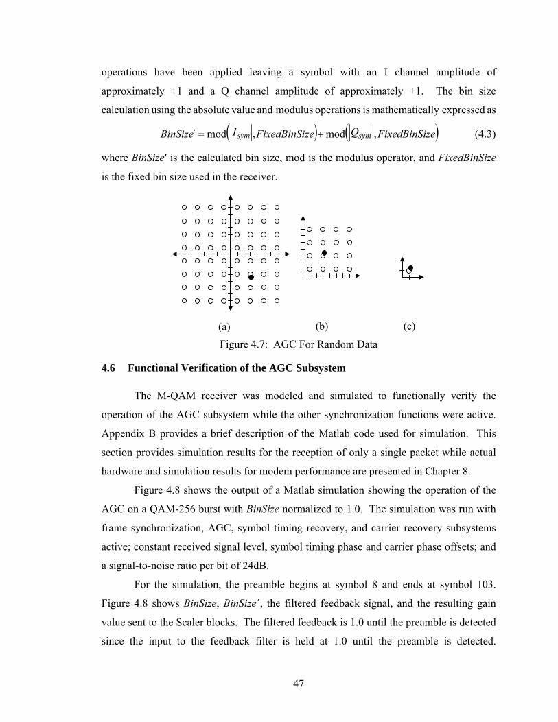
47
operations have been applied leaving a symbol with an I channel amplitude of
approximately +1 and a Q channel amplitude of approximately +1. The bin size
calculation using the absolute value and modulus operations is mathematically expressed as
( ) ( )zeFixedBinSiQzeFixedBinSiIeBinSiz symsym ,mod,mod +=′ (4.3)
where BinSize′ is the calculated bin size, mod is the modulus operator, and FixedBinSize
is the fixed bin size used in the receiver.
(a) (b) (c) Figure 4.7: AGC For Random Data
4.6 Functional Verification of the AGC Subsystem
The M-QAM receiver was modeled and simulated to functionally verify the
operation of the AGC subsystem while the other synchronization functions were active.
Appendix B provides a brief description of the Matlab code used for simulation. This
section provides simulation results for the reception of only a single packet while actual
hardware and simulation results for modem performance are presented in Chapter 8.
Figure 4.8 shows the output of a Matlab simulation showing the operation of the
AGC on a QAM-256 burst with BinSize normalized to 1.0. The simulation was run with
frame synchronization, AGC, symbol timing recovery, and carrier recovery subsystems
active; constant received signal level, symbol timing phase and carrier phase offsets; and
a signal-to-noise ratio per bit of 24dB.
For the simulation, the preamble begins at symbol 8 and ends at symbol 103.
Figure 4.8 shows BinSize, BinSize´, the filtered feedback signal, and the resulting gain
value sent to the Scaler blocks. The filtered feedback is 1.0 until the preamble is detected
since the input to the feedback filter is held at 1.0 until the preamble is detected.

48
Therefore, the gain remains 1.0 until the preamble is detected. The spike in the filtered
feedback signal at symbol 8 is the result of a false frame detection. However, the frame
detection circuit resets on symbol 9 after it determines the initial frame synchronization
was incorrect and the feedback signal is reset to 1.0. At symbol 15, the preamble has
been correctly detected and the feedback signal begins to react to the amplitude of the
received signal. The gain effectively stabilizes in 30 preamble symbols. Once stable, the
gain is tracked throughout the preamble.
At symbol 104, the input to the feedback filter is switched to BinSize´ when the
data segment begins. The plots of BinSize and BinSize´ clearly show the superior
performance of BinSize´ as an amplitude estimate during the data segment of the burst
where the noise of BinSize´ is considerably smaller than BinSize and BinSize no longer
has an average value of 1.0.
20 40 60 80 100 120 140 1600
0.5
1
1.5
2
Bin
Siz
e
20 40 60 80 100 120 140 1600
0.5
1
1.5
Bin
Siz
e’
20 40 60 80 100 120 140 1600.5
1
1.5
Filt
erd
Fee
dbac
k
20 40 60 80 100 120 140 1600.5
1
1.5
Gai
n
Symbol Figure 4.8: Operation of the AGC
49
Chapter 5
Symbol Timing Recovery
5.1 Overview
In a digital communications system, the received signal must be sampled
periodically at the symbol rate with a phase that is optimal. To do this, the receiver
maintains a variable phase sample clock that triggers the sampling process. However,
because the transmitter and receiver use different reference oscillators, symbol timing
offsets are inevitable. The process of synchronizing the sample clock, generated from the
reference oscillator in the receiver, with the received signal is called symbol timing
recovery and it is performed by the Clock Recovery block shown in Figure 3.3.
Figure 5.1 shows an eye diagram and three possible symbol clocks that illustrate
the importance of symbol timing recovery for a QAM-256 signal. The eye diagram
consists of a plot of signal amplitude against time for a fixed number of symbol periods.
After the fixed number of periods has been reached, the amplitude versus time trace
begins again on the left side of the plot so that a large number of traces overlap. In the
case of QAM, either the I channel amplitude or the Q channel amplitude is plotted after
passing through the RRC filter in the receiver.
On the eye diagram, the vertical dotted lines show the optimal sampling points.
The eye diagram gets its name from the eye shaped spaces centred at the optimal
sampling points where no traces pass. The size of the “eyes” gives an indication of the
noise margin and the timing margin for the received signal. The height of eyes indicates
the noise margin or the amount of additional additive noise required to cause errors. The
width of the eyes indicates the timing margin or how large of an offset in the symbol
clock is necessary to cause errors.
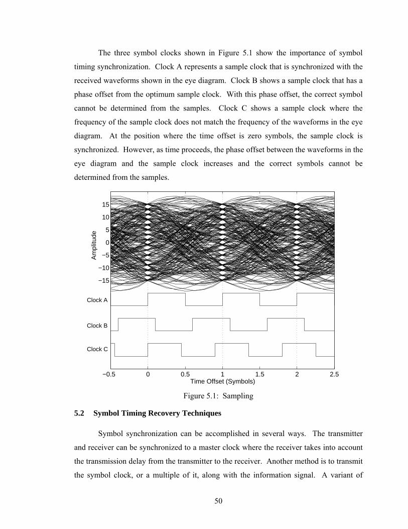
50
The three symbol clocks shown in Figure 5.1 show the importance of symbol
timing synchronization. Clock A represents a sample clock that is synchronized with the
received waveforms shown in the eye diagram. Clock B shows a sample clock that has a
phase offset from the optimum sample clock. With this phase offset, the correct symbol
cannot be determined from the samples. Clock C shows a sample clock where the
frequency of the sample clock does not match the frequency of the waveforms in the eye
diagram. At the position where the time offset is zero symbols, the sample clock is
synchronized. However, as time proceeds, the phase offset between the waveforms in the
eye diagram and the sample clock increases and the correct symbols cannot be
determined from the samples.
−0.5 0 0.5 1 1.5 2 2.5
−15
−10
−5
0
5
10
15
Time Offset (Symbols)
Am
plitu
de
Figure 5.1: Sampling
5.2 Symbol Timing Recovery Techniques
Symbol synchronization can be accomplished in several ways. The transmitter
and receiver can be synchronized to a master clock where the receiver takes into account
the transmission delay from the transmitter to the receiver. Another method is to transmit
the symbol clock, or a multiple of it, along with the information signal. A variant of
Clock A
Clock B
Clock C

51
transmitting the symbol clock along with the information is to send a periodic “sounding
sequence”. The receiver searches for the “sounding sequence” in order to set a sample
clock that is then used until another “sounding sequence” is received. These techniques
are simple; however, the transmitter must allocate some of its power and bandwidth to
transmit the clock signal [10]. The sample clock can also be extracted from the received
data signal. The process of extracting the sample clock from the received data is known
as self-synchronization.
Common self-synchronization techniques include times-two, maximum
amplitude, early-late gate, and zero crossing techniques. Each of these techniques works
well with random data and synchronization can be accelerated for burst-mode operation
by using preamble sequences that have certain properties.
5.2.1 Times-Two Symbol Timing Recovery
The times-two timing recovery technique relies on the property that a typical data
signal contains repetitive sequences of symbols that have alternately positive and
negative amplitudes [35]. These sequences will contain a frequency component at half of
the symbol rate. If the signal is squared, the frequency component at half of the symbol
rate will be doubled or multiplied “times-two” in the frequency domain. This results in a
frequency component at the symbol rate. A narrow bandpass filter can be used to extract
a sample clock from the squared signal.
This technique works well for QAM-4 where the probability of a repeating
sequence with symbols that have alternately positive and negative amplitudes is relatively
high. However, as the modulation level increases and more constellation points are
possible, the technique is less effective due to a lower probability of a repeating sequence
of symbols [35].
5.2.2 Maximum Amplitude Symbol Timing Recovery
The maximum amplitude synchronization technique is derived from the maximum
likelihood estimation technique. The technique relies on the property that, when
averaged over a number of symbols, the absolute value of the amplitude of a signal is
highest at the optimum sample point as shown in Figure 5.2 [27, 22].

52
0 -0.5 0.5Time
(Symbols from the Optimum Sample Point)
Ave
rage
of |
Am
plitu
de|
Figure 5.2: Average Symbol Amplitude as a Function of Time
The maximum amplitude synchronization technique is implemented by over-
sampling the received signal by a factor of J samples per symbol. This gives J equally
spaced phase options for sampling the received signal. From the samples, J running
averages are calculated, one for each phase option. From these, the phase option with the
largest running average is used as a sample point for recovering data from the received
signal.
5.2.3 Early-Late Symbol Timing Recovery
The early-late synchronization technique also relies on the property that, when
averaged over a number of symbols, the absolute value of the amplitude of a signal is
highest at the optimum sample point [27, 22]. However, unlike the maximum amplitude
synchronization technique that samples the received signal J times per symbol, the early-
late synchronization technique samples three times per symbol: one at the phase offset the
receiver believes is optimum, one δ symbols before the phase offset the receiver believes
is optimum, and one δ symbols after the phase offset the receiver believes is optimum [8].
If the receiver is actually sampling at the optimum phase offset, as shown in Figure 5.3,
the average of the absolute value of the early sample will equal the average of the
absolute value of the late sample. If the receiver is sampling at a point that is not the
optimum phase offset, the early and late averages will not be equal. Thus, the difference

53
between the average early sample and the average late sample can be used to advance or
retard a sample clock [35].
0 -0.5 0.5Time
(Symbols from the Optimum Sample Point)
Ave
rage
of |
Am
plitu
de|
Average Early
Sample
Average Optimum Sample
Average Late Sample
δ -δ
Figure 5.3: Early-Late Sampling
5.2.4 Zero Crossing Symbol Timing Recovery
The zero crossing synchronization technique relies on the property that, on
average, zero crossings occur half a symbol before the optimum sample point.
Figure 5.4, an eye diagram generated from a random QAM-4 sequence, confirms the
0 0.5 1−2
−1
0
1
2
Time (Symbols)
Am
plitu
de
Figure 5.4: QAM-4 Eye Diagram

54
relative location of the zero crossings and the optimal sample point. If the sample clock
is causing sampling to occur too early, the average zero crossing will occur more than a
half symbol after the sampling time. Thus, the delay between the sampling time and zero
crossing can be used to advance or retard a sample clock [22, 26, 35].
In previous work, zero crossing timing recovery has not been widely applied to
modems implemented in digital logic or to modems operating on complex constellations.
The main impediment to implementation in digital logic is that added complexity results
from the need to interpolate the location of the zero crossing from the digital samples.
The drawback of zero crossing timing recovery in large constellations is the presence of
large zero crossing jitter and a large number of symbol transitions that do not cross
zero [35]. However, work by Aspel and Klymyshyn [34] has shown that the zero
crossing technique can be extended to operate on complex constellations by using the
crossing of a predicted edge amplitude (as described in Section 5.3.1) instead of a zero
crossing.
The predicted edge crossing technique overcomes both the zero crossing jitter of
symbol transitions that cross the zero amplitude level and allows the use of symbol
transitions that do not cross zero. Since the predicted edge amplitude is decision directed,
the technique is not affected by statistical zero crossing randomness introduced by the
data sequence. Therefore, predicted edge crossing technique results in superior tracking
when the BER is low [10]. Also, transitions that do not cross zero will still cross
predicted amplitude thresholds. Hence, the predicted edge crossing technique is a good
choice for the M-QAM data systems since low BERs are desired and there are many
symbol transitions that do not cross zero.
5.3 Predicted Edge Crossing Symbol Timing Recovery System
The implementation of the synchronizer is shown in Figure 5.5. A phase detector
is used to detect whether the edge, if one occurs, is early or late. To maximize the
chances of getting an edge for each symbol, the phase detector checks both the I channel
and Q channel for edges. The output of the phase detector then controls a series of
counters that, together with the phase detector, act as a Digital Phase Locked Loop
(DPLL) to produce a sample clock.

55
Up Carry
K Counter Control Logic
Divide by N Counter
Sample Clock
I Channel Samples
Borrow
Phase Detector
DownLimit
Q Channel Samples
Figure 5.5: Simplified Zero Crossing Symbol Timing Recovery Implementation
5.3.1 Phase Detector
The phase detector must determine whether the receiver is sampling the received
signal early or late in order to generate a “count up” or “count down” signal for the K
Counter. The phase detector does this by determining whether an edge occurs before or
after the halfway point between samples that correspond to symbols. For a sequence of
alternately positive and negative symbols with equal amplitude, as shown in Figure 5.6,
an edge occurs when the signal trajectories of the I or Q channels cross zero. Thus, the
phase detector will behave just as if it were part of a zero crossing symbol timing
recovery system for these sequences. For other symbol sequences, an edge occurs when
the signal trajectory crosses a value that is equal to the amplitude of the signal trajectory
halfway between the ideal symbol points.
Edge detection is easily done in analog circuitry. In digital circuitry, edge
detection requires over-sampling and the accuracy of the edge location is determined by
the sampling rate. However, whether the edge occurred early or late can be inferred from
a sample halfway between symbols and whether the slope of the curve is positive or
negative. Figure 5.6 shows the filtered sample points for a received signal that is sampled
four times per symbol. ICurrent and QCurrent are the I and Q channel samples for the
current symbol while IOld and QOld are the samples for the previous symbol. IEdge and
QEdge are the samples halfway between the current and previous symbols. Since the
symbols are alternately positive and negative symbols and have equal amplitude, the

56
amplitude of IEdge and QEdge should be zero when the received signal is being sampled
optimally. Furthermore, whether the slope is positive or negative is determined by
whether the current or previous symbol is larger. Thus, the expressions that show
whether the I and Q channel edges occurred early are
( ) ( )OldCurrentEdge III >⊕> 0 (5.1)
( ) ( )OldCurrentEdge QQQ >⊕> 0 (5.2)
where ⊕ is the exclusive OR operator.
I Channel
Q Channel
Last Symbol
Point
CurrentSymbol
Point
CurrentEdge Point
RRC Filter Outputs
ICurrent
IOld
IEdge
QCurrent
QEdge
QOld
Approximate Slope
Figure 5.6: Sampled Points for I and Q for a QAM-4 Signal
For sequences that do not consist of alternately positive and negative symbols
with equal amplitude, as shown in Figure 5.6, the ideal amplitude of the edge is not zero.
Figure 5.7 shows the variation in edge amplitude in random QAM-4 and QAM-16 data
transitions. The traces consist of two categories of transitions: transitions that have
different initial and final amplitudes and transitions that have initial and final amplitudes
that are equal. Only transitions that have different initial and final amplitudes are used by

57
the phase detector since transitions that have initial and final amplitudes that are equal
have relatively flat signal trajectories.
0 0.5 1−2
−1
0
1
2
Time (Symbols)
Am
plitu
de
0 0.5 1
−5
−4
−3
−2
−1
0
1
2
3
4
5
Time (Symbols)
Am
plitu
de
(a) (b)
Figure 5.7: Zero Crossing Jitter
To utilize transitions in random data, IEdge and QEdge are compared to the predicted
values IPred and QPred, which are the expected values of IEdge and QEdge as shown in Figure
5.8. Thus, the expressions given in Equations 5.3 and 5.4 show whether the I and Q
channel edges occurred early in random data.
( ) ( )OldCurrentPredEdge IIII >⊕> (5.3)
( ) ( )OldCurrentedEdge QQQQ >⊕> Pr (5.4)
Accurate estimation of the edge amplitude is complicated by Inter-Symbol
Interference (ISI) at the edge points. Pre-filtering techniques [23, 24, 25, 36] can be used
to reduce this inter-symbol interference so that linear interpolation may be used. An
alternative approach uses compact digital prediction filters to predict the edge value,
including ISI, from the decoded symbol values. This results in accurate prediction of the
edge amplitudes since uncorrupted signal trajectories based on the received symbol
sequence are used. This also results in smaller filters since only decoded symbols are
used as filters inputs compared to pre-filtering techniques where all samples are used.
The prediction filters used to calculate IPred and QPred are Finite Impulse Response
(FIR) filters with an impulse response that matches the combined response of the RRC
filters in the transmitter and the RRC filters in the receiver. The inputs to the prediction
filters are decoded symbol points (±1, ±3, …). Symbol errors that occur result in
incorrect edge predictions and sample clock jitter. This tends to be averaged out in the

58
Predicted RRC Filter O utputs
I Channel
Q Channel
CurrentEdge Point
RRC Filter O utputs
IEdge
Q Edge Q Pred
IPred
CurrentSym bol
Point
Last Sym bol
Point
N ext Sym bol
Point
Figure 5.8: Expected Edge Values
feedback loop unless symbol errors become excessive. The outputs of the filters are
taken from the appropriate tap and multiplied by BinSize/2 to get IPred and QPred. To
obtain good performance, the prediction filter uses symbols before and after the current
edge. To do this, the edge values are queued in a three element First In First Out (FIFO)
buffer so that the correct edge value is compared to the correct predicted edge value.
This results in increased loop delay but the delay is tolerable and does not significantly
affect tracking adjustments required during the data segment of the burst.
The phase detector uses Equations 5.1 and 5.2 during the preamble, since the
expected edge values are always zero due to alternately positive and negative symbols
with equal amplitude. Equations 5.3 and 5.4 are used for random data when the expected
edge values vary dramatically. During the preamble, a “count up” signal is generated if
Equations 5.1 and 5.2 are true while a “count down” signal is generated if the expressions
are both false. This results in operation that parallels a zero crossing symbol timing
recovery system. During the data segment of a burst, a “count up” signal is generated if
Equations 5.3 and 5.4 are true while a “count down” signal is generated if the expressions

59
are both false. This results in tracking with much less jitter than that of a zero-crossing
symbol timing recovery system.
5.3.2 N Counter
The N counter consists of a binary counter that counts from zero to a limit that is
indicated by the Control Logic. The counter outputs four equally spaced pulses per
symbol when the counter equals 0, 0.25 times the limit, 0.5 times the limit and 0.75 times
the limit. Each pulse triggers the A/D converter to sample the received waveform. The
counter, and thus the sampling pulses, is advanced or retarded by increasing or decreasing
the limit for one cycle of the counter.
The N counter also provides a two-bit number that indicates which of the four
samples per symbol each sample represents: 0 indicates that the current sample is the
optimum symbol point and 2 indicates that the current symbol is a zero crossing or
“edge” point.
5.3.3 K Counter and Control Logic
The K counter is a variable size up-down counter that is incremented or
decremented once per symbol. When the counter generates either a carry or a borrow
signal, the control logic is signaled to advance or retard the sample clock by modifying
the limit that is sent to the N counter.
The size of the K counter determines the loop bandwidth [37]. To obtain the best
possible BER, a small loop bandwidth is desirable for tracking since it averages the noise
from the phase detector. However, a small loop bandwidth greatly increases the response
time of the DPLL and thus the acquisition time [38]. Therefore, the effective size of the
K counter is modified by dynamically changing the step size during the acquisition and
tracking portions of the burst. A diagram of the K counter is shown in Figure 5.9.
The M-QAM system designed for this thesis uses a repeating +a, -a, -a, +a
sequence in the preamble. This sequence results in both the I channel and the Q channel
receiving a repeating +a, -a sequence that ensures all of the zero crossings in the
preamble are exactly one-half symbol from the optimal symbol point. This allows a
larger loop bandwidth to be used in the preamble, resulting in faster acquisition than

60
would be possible for random data. Furthermore, jitter can be better tolerated in the
QAM-4 constellation of the preamble than the data segment where small symbol timing
offsets can lead to bit errors in more complex constellations when M>4.
Carry
Borrow
Up
Down
+
-
z-1
G1
Sum
Bandwidth Control
Figure 5.9: Adjustable K Counter
The acquisition speed can also be increased by changing how much the N counter
limit is modified. Normally, the control logic modifies the limit by ±1. However, this
limit can be modified by a larger value at the beginning of the preamble to roughly
synchronize the sample clock with the received signal. For the implemented modem, the
N counter limit is initially modified by ±16 but as the preamble continues, the limit is
modified by smaller and smaller values until it is modified by ±2 on the fiftieth symbol.
The limit is not modified by ±1 due to limitations in the A/D circuitry used.
5.3.4 Symbol Timing Frequency Offsets
The symbol timing recovery system, described in Section 5.3.1 through Section
5.3.3, represents a Type I Phase Locked Loop (PLL). A Type I PLL can completely
remove a phase offset between two signals at the same frequency. However, a Type I
PLL will always have a residual phase error if the two signals are at different frequencies.
The residual phase error is proportional to difference in the frequencies of the two
signals.
The residual error present in a Type I PLL from frequency differences can be
avoided if a Type II PLL is used instead of a Type I PLL [30]. Therefore, a Type II PLL

61
is used for the implemented modem architecture. The Type II PLL is implemented by
adding a second feedback loop to the K counter as shown in Figure 5.10. Conceptually,
the second feedback loop keeps track of trends in the input to the original feedback loop
and provides additional input of the same polarity. Trends in the input to the original
loop come from the phase of the received symbol timing moving away from the local
symbol clock due to a frequency offset between the transmit symbol clock and the
receive symbol clock. By detecting the trends with a second feedback loop, the PLL can
anticipate and correct for phase drift due to a frequency offset.
Up
Down
+
-
z-1
Carry
Borrow
z-1
Sum
Bandwidth Control
Second Feedback Loop
Figure 5.10: Second Order K Counter
5.4 Functional Verification of the Symbol Timing Recovery Subsystem
The M-QAM receiver was modeled and simulated to verify the functional
operation of the symbol timing recovery subsystem while the other synchronization
functions were active. Appendix B provides a brief description of the Matlab code used
for simulation. This section provides simulation results for the reception of only a single
packet while actual hardware and simulation results for modem performance are
presented in Chapter 8.
Figure 5.11 shows the output of a Matlab simulation showing the operation of the
symbol timing recovery subsystem on the same QAM-256 burst described in Section 4.6.
The simulation was run with frame synchronization, AGC, symbol timing recovery, and
carrier recovery subsystems active; constant received signal level, symbol timing phase
and carrier phase offsets; and signal-to-noise ratio per bit of 24dB.

62
Excluding the data segment of the burst, the timing recovery compares the actual
edge values to zero. For the simulation, the preamble begins at symbol 8 and ends at
symbol 103. The symbol timing recovery synchronizes with the received signal within
approximately 30 symbols of the start of the preamble. Once synchronized, the measured
edge values are very close to zero due to the repeating sequence of alternately positive
and negative symbols that is transmitted on each of the I and Q channels.
During the data segment of the burst, the timing recovery compares the actual
edge values to predicted edge values that are shown by circles in Figure 5.11. The plots
show that the system can accurately predict the amplitude of the edges.
The last few symbols of the preamble have measured edge values that can differ
significantly from the expected value of zero due to encoding that signals the end of the
preamble and the constellation size for the data segment. Therefore, the last two symbols
of the preamble are compared to predicted values just as the data segment of the burst.
20 40 60 80 100 120 140−15
−10
−5
0
5
10
15
I cha
nnel
Edg
es
ActualPredicted
20 40 60 80 100 120 140−15
−10
−5
0
5
10
15
Q c
hann
el E
dges Actual
Predicted
20 40 60 80 100 120 140−1
0
1
Out
put P
hase
(*p
i rad
)
Symbol Figure 5.11: Operation of the Symbol Timing Recovery Subsystem

63
Chapter 6
Carrier Recovery
6.1 Overview
There are two methods of demodulation: non-coherent and coherent. Non-
coherent demodulation does not require the carrier to be known while coherent
demodulation requires the carrier to be known. Some modulation schemes such as
amplitude modulation or differential phase shift modulation can be demodulated with
non-coherent demodulation techniques. Other modulation schemes such a QAM, which
require knowledge of the absolute phase of the carrier, can only be demodulated
coherently.
There are two techniques for coherent demodulation in QAM. The first uses an
adjustable local oscillator for quadrature demodulation. The second uses a fixed local
oscillator for quadrature demodulation and then compensates for phase and frequency
offset using a derotator as shown in Figure 3.3. The second technique also reduces the
delay in the carrier recovery feedback loop when a feedback technique is used for carrier
recovery. The delay is shorter with the derotator because the RRC filter, and its
associated group delay, is not within the feedback loop. For this reason, the second
technique was implemented.
6.2 Need For Carrier Recovery
If the local oscillator in the receiver is not synchronized with a received QAM
signal, the data cannot be correctly recovered from the received signal. Figure 6.1 shows
the effect of phase and frequency offsets in the local oscillator. Figure 6.1a shows a
QAM-64 constellation that has been demodulated with a local oscillator that has no phase

64
or frequency offset. Figure 6.1b shows the same constellation except that the local
oscillator has a 10 degree phase offset. In this case, the constellation is rotated by 10
degrees causing bit errors by moving some of the constellation points across decision
lines. Figure 6.1c shows the same constellation except that the local oscillator has a
frequency offset. In this case, the constellation points do not remain in the same position
since the phase is constantly changing. Therefore, the constellation points trace out a
circular locus as the phase changes with time.
(a) (b) (c)
Figure 6.1: Effect of Carrier Phase and Frequency Offset
The effect of a phase error in QAM can be derived mathematically [10].
A QAM signal, s(t), may be represented as shown in Equation 6.1
( ) ( ) ( ) ( )φπφπ +−+= tftAtftAts cQcI 2sin2cos)( (6.1)
where AI(t) is the amplitude of the in-phase component as a function of time, AQ(t)
is the amplitude of the quadrature component as a function of time, fc is the
carrier frequency, and φ is the phase of the carrier that was modulated. If the QAM
signal is demodulated by cI(t) and cQ(t), shown in Equation 6.2 and Equation 6.3,
( )dcI tftc φπ += 2cos)( (6.2)
( )dcQ tftc φπ +−= 2sin)( (6.3)
where dφ is the phase of the signals being used to demodulate s(t), then
the recovered in-phase component, AI´(t), will be given by Equation 6.4 and
the recovered quadrature component, AQ´(t), will be given by Equation 6.5.

65
( ) ( ) ( ) ( )dQdII tAtAtA φφφφ −−−=′ sin21cos
21)( (6.4)
( ) ( ) ( ) ( )dIdQQ tAtAtA φφφφ −+−=′ sin21cos
21)( (6.5)
From Equation 6.4 and Equation 6.5, it is evident that the amplitudes AI´(t) and AQ´(t) are
reduced to ( )dφφ −cos times their amplitudes if there was no phase offset. Since power
is proportional to the square of the amplitude, the powers of AI´(t) and AQ´(t) are reduced
to ( )dφφ −2cos times their powers if there was no phase offset. Equation 6.4 and
Equation 6.5 also show that crosstalk is introduced between the in-phase and quadrature
components.
6.3 Carrier Recovery Techniques
There are two categories of techniques for carrier synchronization: assisted and
blind. Assisted techniques multiplex a special signal called a pilot signal with the data
signal. Blind synchronization techniques derive the carrier phase estimate directly from
the modulated signal. This approach is more prevalent in practice and has the advantage
that all of the transmitter power can be allocated to the information-bearing signal [10].
6.3.1 Pilot Tone Assisted Carrier Recovery
A system that uses pilot tone assisted carrier recovery multiplexes an un-
modulated tone with the information signal. The tone is commonly added at either the
carrier frequency, as shown in Figure 6.2, or a multiple of the carrier frequency. The
receiver then uses a phase locked loop to acquire and track the carrier component. The
Frequency
Am
plitu
de
Pilot Tone
Information Signal
Figure 6.2: Signal with Embedded Pilot Tone

66
phase locked loop is designed to have a narrow bandwidth so that the information signal
does not significantly affect the recovered carrier estimate [10].
6.3.2 Squaring Loop
The square-law device is widely used to estimate the carrier phase of suppressed
carrier signals such as PAM. For PAM, there is no coherent energy at the carrier
frequency so a band-pass filter centred at the carrier frequency cannot be used to recover
the carrier from the received signal. However, the received signal can be squared to
generate a frequency component at twice the carrier frequency [10]. This frequency
component can be used to drive a PLL to create a signal synchronized with the carrier
signal. This technique is illustrated in Figure 6.3.
Unfortunately, the squaring approach does not work well for QAM. When a
QAM signal with equal power in each quadrature branch is squared, the signal power in
each branch tends to cancel leaving a low signal level with which to perform carrier
recovery. However, this can be overcome by using a fourth power loop [28, 39].
Received Signal
Recovered Carrier
Square-law Device
Band-pass filter tuned to 2fc
Loop Filter
VCO
÷2
Figure 6.3: Square-Law Based PLL for Carrier Recovery
6.3.3 Costas Loop
The Costas loop, developed in 1956, can recover the carrier from suppressed
carrier signal in a similar manner to the squaring loop. However, the Costas loop can
recover the carrier phase of a QAM signal [28]. A block diagram is shown in Figure 6.4.
The received signal is multiplied by the recovered carrier and a version of the recovered
carrier that has been shifted by 90 degrees. The results from each of these operations are
low-pass filtered and multiplied together to generate an error signal that is used to drive a
Voltage Controlled Oscillator (VCO).

67
Received Signal
Low-pass Filter
Low-pass Filter
VCO Loop Filter
Recovered Carrier
90º Phase Shift
Figure 6.4: Costas Loop
6.3.4 Decision Feedback Phase Locked Loop
Both the squaring loop and the Costas loop treat the information signal as a
random sequence and use its statistical average to recover the carrier information
embedded within it. A decision feedback PLL, shown in Figure 6.5, assumes that the
information sequence is known. For the decision feedback PLL shown in Figure 6.5, the
data sequence is obtained from the received signal by the QAM Detector. Therefore, the
phase contribution of each symbol can be removed in the phase detector before
calculating an error signal once per symbol.
Received Signal
Matched Filter
Matched Filter
VCO
90º Phase Shift
Loop Filter
Recovered Carrier
Sampler
Phase Detector
QAM Detector
Sampler
Symbol Timing
Symbol Timing
Q
I
Decoded Symbol
Figure 6.5: Decision Feedback PLL for QAM
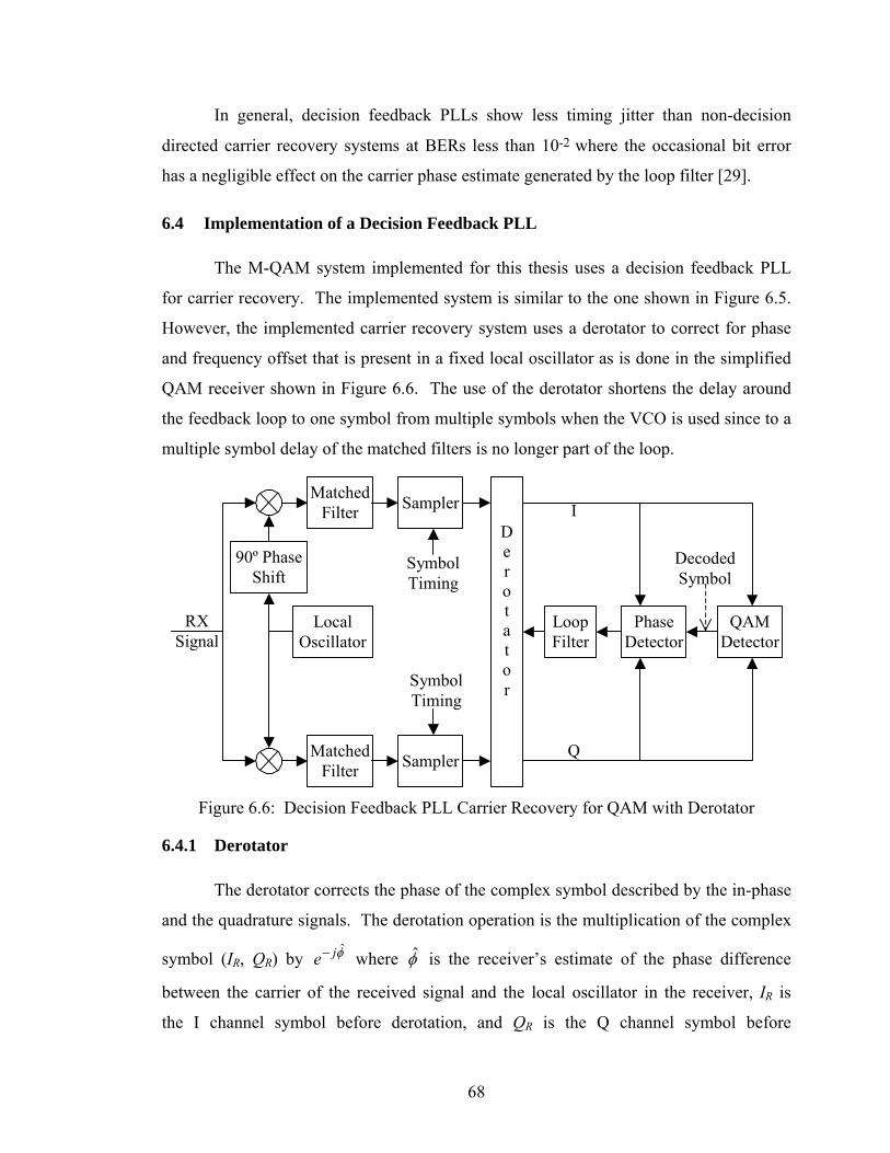
68
In general, decision feedback PLLs show less timing jitter than non-decision
directed carrier recovery systems at BERs less than 10-2 where the occasional bit error
has a negligible effect on the carrier phase estimate generated by the loop filter [29].
6.4 Implementation of a Decision Feedback PLL
The M-QAM system implemented for this thesis uses a decision feedback PLL
for carrier recovery. The implemented system is similar to the one shown in Figure 6.5.
However, the implemented carrier recovery system uses a derotator to correct for phase
and frequency offset that is present in a fixed local oscillator as is done in the simplified
QAM receiver shown in Figure 6.6. The use of the derotator shortens the delay around
the feedback loop to one symbol from multiple symbols when the VCO is used since to a
multiple symbol delay of the matched filters is no longer part of the loop.
RX Signal
Matched Filter
Matched Filter
Local Oscillator
90º Phase Shift
Loop Filter
Sampler
Phase Detector
QAM Detector
Sampler
Symbol Timing
Symbol Timing
Q
I
Decoded Symbol
Derotator
Figure 6.6: Decision Feedback PLL Carrier Recovery for QAM with Derotator
6.4.1 Derotator
The derotator corrects the phase of the complex symbol described by the in-phase
and the quadrature signals. The derotation operation is the multiplication of the complex
symbol (IR, QR) by φje− where φ is the receiver’s estimate of the phase difference
between the carrier of the received signal and the local oscillator in the receiver, IR is
the I channel symbol before derotation, and QR is the Q channel symbol before

69
derotation. This operation can also be represented by Equation 6.6 and Equation 6.7.
( ) ( )φφ ˆsinˆcos RR QII += (6.6)
( ) ( )φφ ˆsinˆcos RR IQQ −= (6.7)
Equation 6.6 and Equation 6.7 can be directly implemented in hardware as shown in
Figure 6.7.
COS lookup table
SIN lookup table
IR
QR
Ø I
Q
+
+
-
+
Figure 6.7: Derotator Implementation
6.4.2 Phase Detector
The phase detector calculates the phase error of each point. During the preamble,
this is an easy task since all symbol points should have a phase of either 45º, 135º, 225º
or 315º. However, during the data segment of each burst, up to 256 constellation points
are present. Together, these 256 constellation points represent many more phase
possibilities.
All square QAM constellations have four quadrants that share rotational
symmetry at 90º intervals. To reduce the number of phase possibilities, the received
symbol ),( QI , shown in Figure 6.8a, is rotated by 0, 90, 180, or 270 degrees to place it
in the first quadrant of the modulation plane based on the signs of I and Q. This results in
a calculation point ),( QI ′′ as shown in Figure 6.8b that reduces the number of phase
possibilities by a factor of four. Therefore, during the preamble, all points should then
have a phase of 45º, and, during the data segment of the burst, the average phase of the

70
constellation points should be 45º. Thus, an error signal can be calculated by
4
tan 1 π−⎟⎟
⎠
⎞⎜⎜⎝
⎛′′
= −
QIEPhase (6.8)
where Ephase is the phase error.
1
1
1
1
-1
-1
(a) (b)
(I,Q) (I´,Q´)
Figure 6.8: Quadrant Rotation
In a non-decision directed carrier recovery system, the phase detector compares
the phase of the received symbol to the average symbol phase as shown in Equation 6.8.
That technique will work very well for (I´, Q´) during the preamble since (I´, Q´) should
always be at 45º when no phase offset is present. However, this will result in
considerable jitter during the data segment of the burst when M>4 since (I´, Q´) will not
always be at 45º.
To reduce jitter during the data segment of the burst, a decision-directed carrier
recovery system is used instead of Equation 6.8. The decision-directed system compares
the location of the received symbol point to the location of the nearest symbol point as
⎟⎟⎠
⎞⎜⎜⎝
⎛−⎟⎟
⎠
⎞⎜⎜⎝
⎛′′
= −−
QI
QIEPhase ˆ
ˆtantan 11 (6.9)
where I is the I channel amplitude of the nearest symbol point and Q is the Q channel
amplitude of the nearest symbol point. The nearest symbol point is used as a reference to
reduce jitter since it is the best estimate of the transmitted symbol. This technique can
significantly lower phase jitter compared to non-decision directed systems when the BER
is low since the occasional symbol error is averaged out by the loop filter.
Ideally, the phase error would be calculated using an arctangent function.
However, the arctangent function in difficult to implement since it requires both a
division operation and a look-up table. Therefore, the arctangent function is replaced by

71
( )4
tan 1 π+−≈⎟
⎠⎞
⎜⎝⎛− XYK
XY
SA (6.10)
where X is a placeholder variable, Y is a placeholder variable, and KSA is a scaling factor.
Thus, to avoid implementing the arctangent function, Equation 6.9 can be written as
( ) ( )[ ]IQIQKE SAPhase ˆˆ −−′−′= . (6.11)
Since the location of the most likely constellation point is described by
( ) ( )( ) ( )( )( )1,floor,1,floorˆ,ˆ +′+′= BinSizeQBinSizeBinSizeIBinSizeQI , (6.12)
where the function floor represents the quotient of its first argument divided by its second
argument rounded down to the nearest integer value, Equation 6.11 can be simplified to
( )( )( ) ( )( )( )[ ]BinSizeIBinSizeIBinSizeQBinSizeQKE SAPhase ,floor,floor ′−′−′−′= . (6.13)
Equation 6.13 can be simplified to use the modulus operation as shown in Equation 6.14.
( ) ( )[ ]BinSizeIBinSizeQKE SAPhase ,mod,mod ′−′= (6.14)
In hardware, this modulus operation can be performed by a bit-wise AND if BinSize
is a power of 2. The hardware implementation of the error calculation is described by
( ) ( )[ ]1&&1&& −′−−′= BinSizeIBinSizeQKE SAPhase (6.15)
where the && operator represents the bit-wise AND operation.
Figure 6.9 shows the effect of replacing the arctangent function with a subtraction
function. These plots were made by uniformly distributing 40,000 points in the first
quadrant of a QAM-256 constellation and measuring the phase error using the six
techniques described below. These results were then compared to the actual phase error
that was calculated using Equation 6.9.
The dotted lines in Figure 6.9 show the Probability Distribution Functions (PDFs)
for the error in the phase error estimate when all points of a QAM-256 constellation are
used for phase error calculation without decision feedback. The dotted line without
circles shows the PDF when the arctangent function is used and the dotted line with
circles shows the PDF when the subtraction function is used. Clearly, there is very little
difference in the performance between the proposed phase error calculation and the
arctangent function when all constellation points are used.
The solid lines in Figure 6.9 show the PDFs for the error in the phase error
estimate when only sample points that are detected as diagonal constellation points of a

72
QAM-256 constellation are used for phase error calculation. The solid line without
circles shows the PDF when the arctangent function is used and the solid line with circles
shows the PDF when the subtraction function is used. In this case, the subtraction
technique for calculating the phase error performs poorly compared to the arctangent
technique. This occurs because the subtraction technique does not take into account the
amplitude of the symbol. The smaller area under the PDFs for “diagonally points only”
compared to the other PDFs is due to the smaller number of constellation points.
−0.2 −0.1 0 0.1 0.20
0.01
0.02
0.03
0.04
0.05
0.06
0.07
0.08
0.09
Phase Estimate Error (rad)
Prob
abilit
y
tan−1(Q’/I’)Q’−I’tan−1(Q’/I’) (diagonal)Q’−I’ (diagonal)tan−1(mod(Q’)/mod(I’))mod(Q’)−mod(I’)
Figure 6.9: Probability Distribution of Phase Error Calculation Error
The dashed lines in Figure 6.9 show the PDFs for the error in the phase error
estimate when all points of a QAM-256 constellation are used for phase error calculation
with decision feedback. The dashed line without circles shows the PDF when the
arctangent function is used and the dashed line with circles shows the PDF when the
subtraction function is used. Clearly, there is very little difference in the performance of
the phase error calculations when translation is used. Therefore, the replacement of the
arctangent function with a subtraction does not significantly impact the performance of
the phase detector. The plot also shows that the decision feedback improves the
operation of the phase detector.

73
6.4.3 Quadrant Ambiguity
The phase detector is unable to resolve phase ambiguities that are multiples of 90
degrees due to rotational symmetry in the QAM constellation. The quadrant ambiguity
generated by the carrier recovery system is resolved by a second layer of carrier recovery
logic. During the repeating ),( aa − , ),( aa− sequence portion of the preamble, rotations
by 90 degrees or 270 degrees are detected by the presence of either a ),( aa symbol or a
),( aa −− symbol. Once detected, rotations of 90 degrees or 270 degrees are corrected by
adding 90 degrees to the rotation angle of the derotator. Then the end of preamble
indicator, ),( aa , is used to detect 180 degree phase offsets since it will appear as
),( aa −− if the received signal is 180 degrees out of phase. If a 180 degree phase offset is
detected, 180 degrees are added to the rotation angle of the derotator.
6.4.4 Loop Filter and Phase Accumulator
The Loop Filter block acts both as a loop filter and as a phase accumulator for the
PLL in the simplified QAM receiver shown in Figure 6.6. The block receives the phase
error from the Phase Detector and the output of the block tells the Derotator how much to
rotate the next received symbol. For the QAM receiver implemented for this thesis, the
loop filter and phase accumulator are implemented inside the Carrier Recovery block
along with the phase detector.
The carrier recovery system needs to correct both phase and frequency offsets
between the received signal and the local oscillator in the receiver. To do this a Type II
PLL is required [30]. If only a Type I PLL is used, the received constellation will be
rotated by an amount proportional to the difference in frequency between the received
signal and the local oscillator in the receiver.
The implementation of the loop filter and the phase accumulator for the second
order PLL is shown in Figure 6.10. The operation of the Loop Filter Block can be
understood by examining the roles of the two accumulators. The accumulator labeled as
the Phase Accumulator adds a scaled version of the phase error plus a frequency error
estimate, ω, to the phase estimate to produce a new phase estimate for each symbol. The
frequency error estimate is generated by a second accumulator that maintains a running
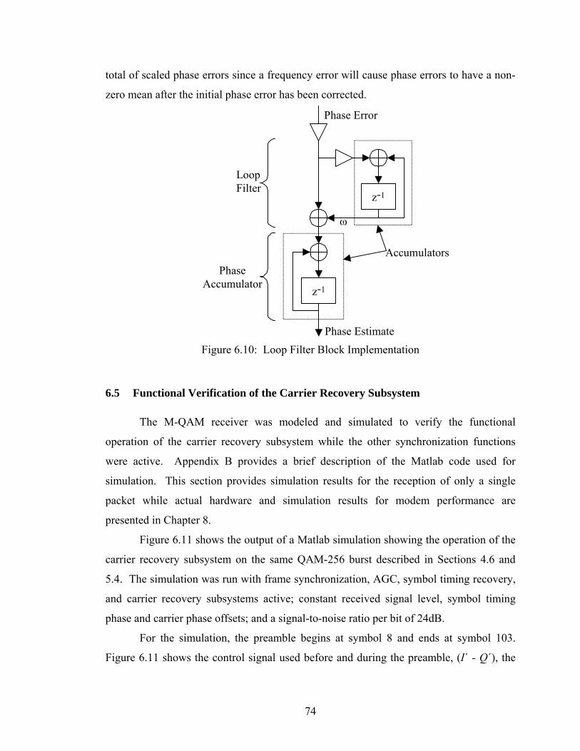
74
total of scaled phase errors since a frequency error will cause phase errors to have a non-
zero mean after the initial phase error has been corrected.
z-1
Phase Error
Phase Estimate
Accumulators
z-1
Loop Filter
Phase Accumulator
ω
Figure 6.10: Loop Filter Block Implementation
6.5 Functional Verification of the Carrier Recovery Subsystem
The M-QAM receiver was modeled and simulated to verify the functional
operation of the carrier recovery subsystem while the other synchronization functions
were active. Appendix B provides a brief description of the Matlab code used for
simulation. This section provides simulation results for the reception of only a single
packet while actual hardware and simulation results for modem performance are
presented in Chapter 8.
Figure 6.11 shows the output of a Matlab simulation showing the operation of the
carrier recovery subsystem on the same QAM-256 burst described in Sections 4.6 and
5.4. The simulation was run with frame synchronization, AGC, symbol timing recovery,
and carrier recovery subsystems active; constant received signal level, symbol timing
phase and carrier phase offsets; and a signal-to-noise ratio per bit of 24dB.
For the simulation, the preamble begins at symbol 8 and ends at symbol 103.
Figure 6.11 shows the control signal used before and during the preamble, (I´ - Q´), the

75
control signal used during the data segment, (mod(I´, BinSize) – mod(Q´, BinSize)), and
the recovered phase. Symbols 0 through 7 show the operation of the carrier recovery
subsystem before the preamble starts. Because the amplitude of the noise is low, very
little phase jitter occurs. Once the preamble begins, the carrier recovery subsystem
synchronizes with the received signal within about 35 symbols.
20 40 60 80 100 120 140−1000
−500
0
500
1000
I’−Q
’
20 40 60 80 100 120 140−1000
−500
0
500
1000
mod
(I’,
Bin
Siz
e) −
mod
(Q’,B
inS
ize)
20 40 60 80 100 120 140−0.75
−0.5
−0.25
0
0.25
Out
put P
hase
(ra
d)
Symbol Figure 6.11: Operation of the Carrier Recovery Subsystem
When the data segment of the burst begins, the carrier recovery subsystem
switches to the (mod(I´, BinSize) – mod(Q´, BinSize)) control signal. Figure 6.11 shows
the reduced jitter of the (mod(I´, BinSize) – mod(Q´, BinSize)) control signal compared to
the (I´ - Q´) control signal as predicted by the probability distribution shown in Figure
6.9.

76
Chapter 7
Filtering
7.1 Overview
The modem system needs a number of filters to operate properly. Figure 3.1
shows a number of filters in the transmitter to limit the bandwidth of the transmitted
signal and receiver to minimize the noise admitted to the receiver. These filters include
pulse shaping Root Raised Cosine (RRC) filters in the transmitter and receiver, IF filters
in the transmitter and receiver, a reconstruction filter in the transmitter and an anti-
aliasing filter in the receiver. Additionally, the clock recovery system requires a
prediction filter as described in Section 5.3.1.
The filtering for the modem is designed with four goals in mind: minimal Inter-
Symbol Interference (ISI), maximum performance in Additive White Gaussian Noise
(AWGN), strong suppression of out-of-band signals, and minimum implementation
complexity.
To achieve zero ISI, the combined response of the filtering at the output of the
transmitter, the channel, and the filtering at the input to the receiver must satisfy
...3,2,10)( === nth nTt (7.1)
where h(t) is the combined response, t is time, and T is the symbol period. A number of
filter responses provide ISI free filtering including the “brick wall” filter response and
raised cosine filter response.
The shape of the filters on the output of the transmitter and the shape of the filters
on the input of the receiver have an impact on the BER performance of the modem
because the filters affect the SNR of the waveform that is demodulated. To achieve the

77
best BER performance, the SNR must be maximized by admitting the maximum amount
of the signal while removing the maximum amount of noise. SNR is maximized for an
AWGN channel when the response of the filters on the output of the transmitter matches
the response of the filters on the input of the receiver [10]. This is known as matched
filtering.
The goals of strongly suppressing of out-of-band signals and implementing the
filtering with minimum complexity were balanced by combining multi-rate digital
filtering with analog filters. In the transmitter, the filtering is implemented as a digital
RRC filter followed by two digital IF filters and then an analog filter. In the receiver, an
analog anti-aliasing filter is followed by two digital IF filters and a digital RRC filter.
7.2 Finite Impulse Response Filters
Finite Impulse Response (FIR) filters are commonly used in communications
systems due to their linear phase response when certain filter coefficients are used. The
RRC filter in the transmitter, the RRC filter in the receiver, and the IF filters are
implemented as FIR filters to take advantage of the linear phase characteristic.
The coefficients of an FIR filter correspond to the magnitude of each sample in a
sampled impulse response. Any FIR filter with coefficients that have symmetry that satisfy
2,...,2,1 Cnbb nCn == − (7.2)
where bn is the nth coefficient and C is the number of coefficients, will have a constant
group delay that is independent of frequency resulting in a linear phase response with a
slope defined by the group delay.
7.3 Square Root Raised Cosine Filters
Raised Cosine (RC) filters are a class of filters that inject no ISI into a signal due
to the shape of their frequency response and their linear phase response. Square Root
Raised Cosine (RRC) filters are a group of filters that produce a raised cosine response
when two of the filters are used in succession. RRC filters are also realizable with
minimal error in digital hardware. Therefore, RRC filters are used as matched filters in
the transmitter and the receiver to produce a raised cosine response. Figure 7.1 shows the
frequency response for three filters in the raised cosine filter family.

78
0
1
-1 -0.5 0 0.5 1Frequency (Normalized by Symbol Rate)
Mag
nitu
de
R=0.0R=0.5R=1.0
Figure 7.1: Raised Cosine Filter Frequency Response
Raised cosine filters are characterized by their roll-off factor, R. When R=0, the
filter has a “brick wall” response that has a flat pass band that extends up to the Nyquist
frequency. When R>0, the response is flat from the centre of the pass band to 0.5-R/2
times the symbol rate while the response follows that of a raised cosine waveform from
0.5-R/2 times the symbol rate to 0.5+R/2 times the symbol rate. The frequency response
of a raised cosine filter is described by its amplitude response and a linear phase
response. The amplitude response, |H(f )|, is given by Equation 7.3 where R is the roll-off
factor, f, is the frequency, and T is the symbol period [10].
⎪⎪⎪
⎩
⎪⎪⎪
⎨
⎧
+≥
+≤≤
−
⎭⎬⎫
⎩⎨⎧
⎥⎦
⎤⎢⎣
⎡⎟⎠⎞
⎜⎝⎛ −
−+
−≤
=
Tf
Tf
TTfT
Tf
fH
2R10
2R1
2R1
2R1
Rcos1
21
2R11
)( π (7.3)
Figure 7.2 shows the impulse responses for the same three raised cosine filters
shown in Figure 7.1. In each case, the impulse response is the inverse Fourier transform
of the frequency responses. Mathematically, the impulse responses, h(t), can be
described by Equation 7.4 [10]. From both Figure 7.2 and Equation 7.4, it is clear that
the impulse response decays much more slowly as R approaches zero. Figure 7.3 shows
that the impulse response for RRC filters also decays much more slowly as R approaches
zero.
( )222 /R41
)/Rcos(/
/sin)(Tt
TtTt
Ttth−
=π
ππ (7.4)

79
−8 −6 −4 −2 0 2 4 6 8−0.5
0
0.5
1
Time (Symbol Periods)
Mag
nitu
de
R=0.0R=0.5R=1.0
Figure 7.2: Raised Cosine Filter Impulse Response
−8 −6 −4 −2 0 2 4 6 8
0
0.5
Time (Symbol Periods)
Mag
nitu
de
R=0.0R=0.5R=1.0
Figure 7.3: RRC Filter Impulse Response

80
Due to the finite nature of the FIR filters, the RRC impulse response is truncated a
finite number of symbols before and after the centre of the response. This truncation
results in a response that has some error. The amount of error depends on the amount of
truncation (determined by the length of the filter) and how quickly the impulse response
decays to zero (determined by the roll-off factor). Therefore, based on the tradeoff
between the error induced by truncation, the need to limit filter size, and the need to use
bandwidth efficiently, a roll-off factor of 0.5 was chosen for this project.
7.3.1 Transmit RRC Filter
The transmit RRC filter consists of 49 taps and generates four ten-bit samples per
symbol that are modulated and sent to the ten-bit D/A converter. Since the filter has 49
taps and generates four samples per symbol, the transmit filter calculates the transmit
waveform based on twelve symbol periods. The filter was generated with a roll-off factor
of 0.5 and the filter coefficients were rounded to ten bits. The ten-bit length of the
coefficients and the use of 49 taps results in the 25th filter coefficient using ten significant
bits and the taps near the edge of the filter using one to two significant bits. Thus,
rounding the coefficients to ten bits makes the error due to filter length truncation
approximately equal to the error due to coefficient truncation.
The filter coefficients were calculated using the rcosfir function in Matlab.
The rcosfir function takes the roll-off factor (0.5), the filter length (6 symbols before
and after the centre of the filter), the sample rate (4 samples per time unit), the symbol
period (normalized to 1 time unit), and the filter type (square root raised cosine) as
parameters.
The largest constellation the M-QAM transmitter can generate is QAM-256.
Therefore, the possible I channel and Q channel symbol values are -15, -13, … 13, 15.
These values can be represented by five bits in two’s complement arithmetic. Hence, the
filter requires five-bit by ten-bit multipliers to calculate the products of five-bit input
values and ten-bit filter coefficients.
Figure 7.4 shows the impulse response and Figure 7.5 shows the magnitude of the
frequency response of the transmit RRC filter. The phase response of the FIR filter is
linear since the filter coefficients are symmetric satisfying the condition in Equation 7.2.

81
0 5 10 15 20 25 30 35 40 45 50−0.2
−0.1
0
0.1
0.2
0.3
0.4
0.5
0.6
Filter Coefficient Number
Impu
lse
Res
pons
e M
agni
tude
Figure 7.4: Transmit RRC Filter Impulse Response
0 0.2 0.4 0.6 0.8 1 1.2 1.4 1.6 1.8 2−100
−80
−60
−40
−20
0
20
Frequency (Normalized by Symbol Frequency)
Mag
nitu
de (
dB)
Figure 7.5: Transmit RRC Filter Frequency Response

82
7.3.2 Receive RRC Filter
The receiver RRC filter consists of 31 taps and operates with four ten-bit samples
per symbol. The filter was generated in Matlab with a roll-off factor of 0.5.
Additionally, the filter coefficients were rounded to eight bits, which makes the error, due
to filter length truncation, approximately equal to the error due to coefficient truncation.
A smaller filter was chosen for the receiver for several reasons. First, multipliers
for ten-bit samples require more FPGA resources than multipliers for five-bit samples
used in the transmitter. By reducing the number of taps and the number of multipliers,
the amount of FPGA resources required for the filter is reduced. Second, the 31 tap filter
introduces less delay in the symbol timing recovery feedback loop since the group delay
is proportional to the length of the filter. This allows faster recovery of the symbol clock
from the received signal.
Figure 7.6 shows the impulse response and Figure 7.7 shows the magnitude of the
frequency response of the RRC filter in the receiver. The phase response of the FIR filter
will be linear since the filter coefficients are symmetric satisfying the condition in
Equation 7.2.
0 5 10 15 20 25 30 35−0.2
−0.1
0
0.1
0.2
0.3
0.4
0.5
0.6
Filter Coefficient Number
Impu
lse
Res
pons
e M
agni
tude
Figure 7.6: Receive RRC Filter Impulse Response

83
0 0.2 0.4 0.6 0.8 1 1.2 1.4 1.6 1.8 2−100
−80
−60
−40
−20
0
20
Frequency (Normalized by Symbol Frequency)
Mag
nitu
de (
dB)
Figure 7.7: Receive RRC Filter Frequency Response
7.4 IF Filters
The analog reconstruction filter needs to strongly suppress adjacent images of the
transmitted signal while not distorting the transmitted signal. Similarly, the anti-aliasing
filter in the receiver needs to strongly suppress signals adjacent to the received signal
without distorting the received signal. This results in high Q requirements for those
filters.
To reduce high Q filtering requirements at the transmitter, the transmitter output is
upsampled by a factor of two, filtered with a high pass filter, upsampled by a factor of
two again, and then filtered with a low pass filter as shown in Figure 7.8. This results in
an output where the third harmonic is present but where the first, fifth and seventh
harmonics are suppressed. Also, very little ISI is introduced into the signal since the
filter pass bands are virtually flat and the filters have a linear phase response as described
in Sections 7.4.1 and 7.4.2.

84
Baseband
2
2
IF
Figure 7.8: TX IF Filtering
By upsampling twice, the speed of the high-pass filter is halved compared to
upsampling by a factor of four and then filtering. Further, by using filters with their
cutoffs at π/2, halfband filters can be used. This is a benefit since every other tap in a
halfband filter is zero resulting in a filter that requires only half as many multipliers.
Similar filtering would be used for the receiver as shown in Figure 7.9. This
digital filtering would decrease the need for very high Q filtering in the receiver IF.
However, IF filtering was not implemented in the receiver for testing since nothing was
being transmitted in adjacent channels and noise injected into the channel was band-
limited.
Baseband
2
2
IF
Figure 7.9: RX IF Filtering
7.4.1 Halfband Filter Design
The number of coefficients in a halfband filter is given by
14 −i (7.5)
where i is an integer. For the IF filters in the M-QAM modem, i was set to 13 resulting in
51 filter coefficients or a filter with an order of 50.
The filter coefficients for the halfband filters were calculated using the remez
function in Matlab and were rounded to ten bits. The remez function takes the filter
order (50), an array of frequency bands ([0 0.45 0.55 1]), an array of amplitudes for the
lower and upper edge of each frequency band ([1 1 0 0] for the low-pass filter and [0 0 1
1] for the high-pass filter), and a weighting that determines the relative importance of
each band ([1 1]). By selecting the correct order, two frequency bands symmetrical about
0.5, and equal weightings for both frequency bands, halfband filters were generated. The
resulting filters had approximately 0.25dB ripple in the pass-band and approximately
45dB attenuation in the stop-band. The filters also had a linear phase response since the
filter coefficients are symmetric satisfying the condition in Equation 7.2.

85
7.4.2 Sin(x)/x Correction and Analog Filter Correction
The frequency of the transmitted signal rolls off with a sin(x)/x shape since the
D/A converter generates pulses that are 1/16th of a symbol wide. In addition, the analog
reconstruction filter, described in Section 7.5, introduces some amplitude distortion into
the transmitted signal. The cumulative effect of these two distortion sources is partially
corrected by modifying the low-pass IF filter so that its frequency response has a slope.
The slope is modified by changing the amplitude vector for the remez function from [1
1 0 0] to [0.967 1.0364 0 0]. This results in a set of coefficients where every other
coefficient is no longer zero. However, since the amplitude specifications are very
similar to those for a halfband filter the coefficients are also very similar to those for a
halfband filter and resulted in only one extra non-zero coefficient after the coefficients
are rounded to ten bits. Additionally, there was no noticeable effect on pass-band ripple
or stop-band attenuation and the phase response was still linear since the coefficients
were still symmetric satisfying the condition in Equation 7.2.
7.5 Reconstruction Filter
A reconstruction filter was used after the digital to analog converter to limit the
bandwidth of the transmitted signal. Bandwidth limiting is required because the D/A
converter generates rectangular pulses. This results in energy at the odd harmonics of the
carrier frequency in addition to energy at the carrier frequency.
The reconstruction filter is a fifth order low pass Butterworth filter as shown in
Figure 7.10. This filter has a 3dB cutoff frequency of 6.0 MHz. Within the spectrum
used by the modem, the filter has a 0.005 symbol variation in group delay and 0.2dB
variation in amplitude.
860nH 2.7µH 860nH
920pF 920pF
Figure 7.10: Reconstruction Filter

86
7.6 Prediction Filter
The prediction filter in the symbol timing recovery subsystem is an FIR filter with
a response equal to the combined response of the transmit RRC filter and the receive
RRC filter. The coefficients were calculated by convolving the coefficients for the
transmit RRC filter with the coefficients for the receive RRC filter. This results in an
array of 79 coefficients that are symmetrical about the 40th coefficient.
The amplitudes of the four symbols detected before an edge and the amplitudes of
three symbols detected after an edge are used for predicting the amplitude of an edge. No
samples between the symbol points are used. Therefore, only seven of the 79 calculated
coefficients are required to predict the edge amplitude based on six symbol periods.
The required coefficients are shown in Figure 7.11. The third and fourth
coefficients that are used correspond to the 38th and 42nd coefficients calculated by the
convolution: two samples (0.5 symbols) from the 40th symbol. The second and fifth
coefficients correspond to the 34th and 46th coefficients: six samples (1.5 symbols) from
the 40th symbol. The first and sixth coefficients correspond to the 30th and 50th
coefficients: ten samples (2.5 symbols) from the 40th symbol. The seventh coefficient
corresponds to the 54th coefficient: fourteen samples (3.5 symbols) from the 40th symbol.
1 2 3 4 5 6 7−0.1
−0.05
0
0.05
0.1
0.15
0.2
0.25
0.3
0.35
0.4
Filter Coefficient Number
Impu
lse
Res
pons
e M
agni
tude
Figure 7.11: Receive RRC Filter Impulse Resonse

87
7.7 Digital Filter Implementation
A conventional FIR filter structure is shown in Figure 7.12 [26]. The filter
consists of registers, multipliers, and one or more adders. The output of each of the Nt
registers is called a tap. Each tap is multiplied by the appropriate filter coefficient, hi,
where i is the tap number, and the products are added together to produce the filter output.
z-1 z-1 z-1 z-1
Σ
X
Y
h0 h1 hNt hNt-1
z-1
Figure 7.12: FIR Filter
RRC and halfband filters have an odd number of symmetric coefficients.
Therefore, the filter architecture used for the RRC and halfband filters can be modified as
shown in Figure 7.13 to reduce the number of multiplications. A similar modification
can be made for the prediction filter to reduce the six multipliers that share coefficients to
three. This reduction in multiplier usage is particularly important for FPGA
z-1 z-1 z-1 z-1
z-1
z-1 z-1 z-1 z-1
Σ
Σ
Σ
Σ
X
Y
h0 h1 h(Nt+1)/2h(Nt+1)/2-1
Figure 7.13: Symmetric FIR Filter

88
implementations of digital filters since multipliers are the most complex and resource
intensive component of the digital filter to implement.
7.8 Canonical Signed Digit Multiplier Filters
Filters that use Canonical Signed Digit (CSD) arithmetic take fewer FPGA
resources to implement than filters that use binary arithmetic. Therefore, the IF filters
were implemented using CSD multipliers to reduce the logic requirements for the filters.
CSD representation represents numbers as summation of powers of two and
powers of two multiplied by -1 while binary representation represents digits by only the
summation of powers of two. Therefore, CSD representation may require fewer non-zero
digits than a binary representation. For example, seven can be represented as 0111
(0*23 + 1*22 + 1*21 + 1*20) in binary format while seven has two possible CSD
representations: 0,+1,+1,+1 (0*23+1*22+1*21+1*20) which has the same number of non-
zero digits or +1,0,0,-1 (1*23+0*22+0*21+-1* 20) which has one less non-zero digit.
The number of logic elements required for a multiplier with one constant input is
proportional to the number of non-zero digits in the constant. CSD multipliers have one
constant input that is represented in CSD format instead of the normal binary format.
Since there are fewer non-zero coefficients in the CSD format, fewer logic blocks are
required to implement the multiplier.
7.9 Serial Filters
Filters that use serial arithmetic take considerably fewer FPGA resources to
implement than filters that use parallel arithmetic. Therefore, both the RRC filters and
the prediction filter are implemented as serial filters. Implementation of serial filters in
FPGAs is discussed in papers published by Altera [40] and Atmel [41].
A diagram showing the structure of a symmetric FIR filter implemented in serial
logic is shown in Figure 7.14. First, the words representing the amplitude of each sample
are converted to a serial bit stream, Least Significant Bit (LSB) first, and clocked into the
filter one bit at a time. The bits then pass through a series of modified shift registers, a
schematic of which is shown in Figure 7.15, that replace the delay elements present in a
standard symmetric FIR filter.

89
SR
SR
SR
SR
SR
SR
SR
Σ
Σ
Σ
Σ
X
Y
h0 h1 h(Nt+1)/2h(Nt+1)/2-1
Carry Save Adder
Serial Multiplier
Σ
Σ
Σ
Σ
Parallel to Serial
Serial to Parallel
Figure 7.14: Serial FIR Filter
z-1 z-1 z-1
SR
Figure 7.15: Modified Shift Register
The serial multipliers take considerably less space parallel multipliers. In an
Altera APEXTM FPGA, eight-bit by ten bit-serial multipliers require approximately 17
logic elements. In contrast, parallel multipliers with one constant coefficient require up
to 95 logic elements depending on what the value of the constant is. Thus, parallel
multipliers would require approximately 800 extra logic elements for each 16 multiplier
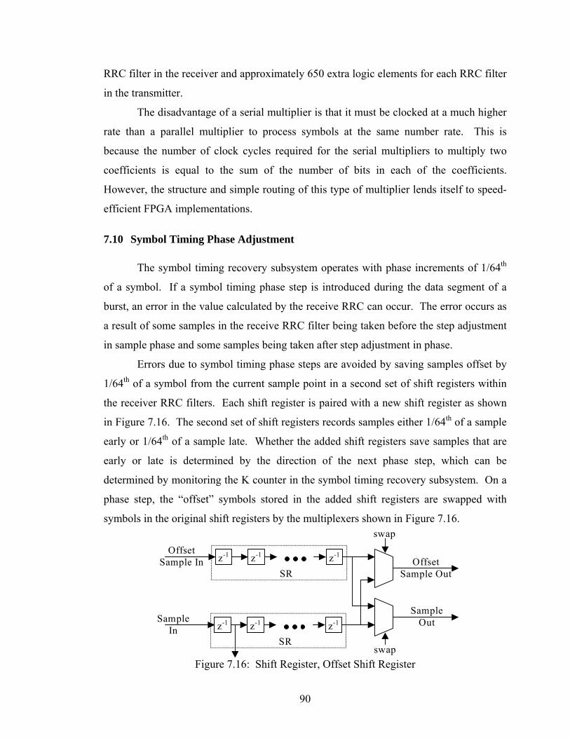
90
RRC filter in the receiver and approximately 650 extra logic elements for each RRC filter
in the transmitter.
The disadvantage of a serial multiplier is that it must be clocked at a much higher
rate than a parallel multiplier to process symbols at the same number rate. This is
because the number of clock cycles required for the serial multipliers to multiply two
coefficients is equal to the sum of the number of bits in each of the coefficients.
However, the structure and simple routing of this type of multiplier lends itself to speed-
efficient FPGA implementations.
7.10 Symbol Timing Phase Adjustment
The symbol timing recovery subsystem operates with phase increments of 1/64th
of a symbol. If a symbol timing phase step is introduced during the data segment of a
burst, an error in the value calculated by the receive RRC can occur. The error occurs as
a result of some samples in the receive RRC filter being taken before the step adjustment
in sample phase and some samples being taken after step adjustment in phase.
Errors due to symbol timing phase steps are avoided by saving samples offset by
1/64th of a symbol from the current sample point in a second set of shift registers within
the receiver RRC filters. Each shift register is paired with a new shift register as shown
in Figure 7.16. The second set of shift registers records samples either 1/64th of a sample
early or 1/64th of a sample late. Whether the added shift registers save samples that are
early or late is determined by the direction of the next phase step, which can be
determined by monitoring the K counter in the symbol timing recovery subsystem. On a
phase step, the “offset” symbols stored in the added shift registers are swapped with
symbols in the original shift registers by the multiplexers shown in Figure 7.16.
z-1 z-1 z-1
SR
z-1 z-1 z-1
SR swap
swap
Sample In
Offset Sample In Offset
Sample Out
Sample Out
Figure 7.16: Shift Register, Offset Shift Register

91
7.11 Transmitted Spectrum
The transmitter was configured to continuously output packets with 144 symbol
preambles, 300 symbols of randomly generated data, and a 20 symbol quiet period
between packets. The transmitter produced a signal centred at three times the symbol rate
of 0.81MHz that was used for testing. That signal, centred at 2.43MHz, is shown in
Figure 7.17. The spectrum is 0.81 mega-symbols per second wide between the -3dB
points. In addition, the signal is 1.22MHz wide between the –40dB points. This matches
the expected width for an RRC roll-off factor of 0.5 and sample rate of 0.81 mega-
samples per second. Similarly, the attenuation due to the RRC filters and the IF filters
was approximately equal to the predicted attenuation described in Sections 7.3 and 7.4.
The spectrum in Figure 7.17 has two spikes at ±0.405MHz from the centre of the
signal. These spikes were due to the repetitive nature of the preamble sequence that
repeated at a rate of 0.405MHz. If 48 symbol preambles were used, the power level of the
spikes would be 4.8dB lower and the spikes would disappear completely if the preamble
length was reduced to zero. As well, the spectrum is for a QAM-256 constellation. Due
to differences in the ratio of preamble power to average data segment power for different
constellations, the difference in power levels between the spikes and the area between the
spikes would decrease by ~2dB for a QAM-4 constellation. Furthermore, the length of
the burst would also affect the difference in power levels between the spikes and the area
between the spikes with longer bursts resulting in smaller differences in power since the
ratio of preamble to data will be reduced.
-80
-70
-60
-50
-40
-30
-20
-10
0
0 0.81 1.62 2.43 3.24 4.05Frequency (MHz)
Rel
ativ
e Po
wer
(dB
)
Figure 7.17: Transmitted Spectrum

92
Chapter 8
Implementation and Performance Results
8.1 Overview
A simplified version of the M-QAM transceiver shown in Figure 3.1 was
implemented for testing. The implemented system is shown in Figure 8.1. Compared to
the system shown in Figure 3.1, the Anti-aliasing Filter and the Digital IF Filtering
modules have been removed from the receiver to simplify implementation. For testing,
the removal of the Anti-aliasing Filter and the Digital IF Filtering modules in the receiver
is possible because no other signals were present in the channel and the channel noise
was band limited.
Baseband MQAM Transmitter
Reconstruction Filter
D/A Digital IF Filtering
Baseband MQAM Receiver
A/D
Transmitter
Receiver
Channel
TX PN Generator
RX PN Generator
BER Calculator
Sync
Figure 8.1: Implemented System Architecture

93
In addition to the M-QAM modem, modules were added to facilitate testing of the
modem. A Pseudo-random Noise (PN) generator was added to create random data for the
transmitter and a second PN generator was added to generate a time delayed copy of the
transmitted data. A bit error rate (BER) calculator was added to compare the PN
sequence to the data steam recovered by the receiver and count both bit errors and packet
errors. Furthermore, the additional modules were implemented such that they did not
affect the performance of the modem.
Although the transmitter and receiver used for testing were on the same FPGA,
separate external master clocks were used for each during testing in order to parallel
practical operation. The TX PN generator and all of the transmitter subsystems shown in
Figure 8.1 are clocked by one clock. The RX PN Generator, the BER Calculator, and all
of the receiver subsystems shown in Figure 8.1 are controlled by a second clock.
Furthermore, the frequency of each clock was adjustable so the frequency offset between
the transmitter and the receiver could be controlled.
The modem was designed to run from a 10MHz crystal oscillator and operate at
one mega-symbol per second. However, the maximum operating frequency varied from
compile to compile of the Verilog source code due to routing and placement algorithms
used by the compiler. Changing the operating frequency posed a problem because the
frequency of the M-QAM signal changed with the operating frequency while the
frequency response of the analog reconstruction filter did not scale in frequency with the
operating frequency. As a result, the transmitted signal passed through slightly different
regions of the reconstruction filter with slightly different responses.
To compensate for variable maximum operating frequency, the operating
frequency of the modem was reduced by approximately 20% to ensure all compiles
would result in implementations that operated at the testing frequency. As a result of the
design of the sin(x)/x correction and analog filter compensation described in Section
7.4.2, the modem performed optimally at 0.81 mega-symbols per second with the
reconstruction filter shown in Section 7.5. The latest compiles indicate the modem would
be capable of operating at one mega-symbol per second if the reconstruction filter or the
sin(x)/x correction and analog filter compensation were re-optimized.

94
8.2 TRLabs FPGA Development system
The M-QAM system, except for the reconstruction filter, amplifier, and channel,
is implemented on a DSP development system designed at TRLabs [42, 43]. A block
diagram of the TRLabs DSP development system is shown in Figure 8.2.
600,000 Gate APEX FPGA
10 bit D/A
10 bit D/A
10 bit D/A
10 bit D/A
12 bit A/D
12 bit A/D 80 Digital IO
XO
VCXO
External Clocks
EEPROM
Programming Port
Figure 8.2: TRLabs FPGA Development Board
The development system is centred on an Altera APEXTM EP20K600EFC672
FPGA [44]. The APEX FPGA can implement up to 600,000 logic gates and is
programmed using a Static Random Access Memory (SRAM) object file. Inside the
FPGA, the configuration is stored in SRAM until the power is cycled.
The logic description for the modem was written in Verilog and an overview of
the code is shown in Appendix A. The Verilog code was compiled into an SRAM object
file with the Quartus II software (version 2.0) from Altera [5]. The SRAM object file
was then loaded onto the development board using a cable connecting the parallel port on
a personal computer to the programming port of the development board.
8.3 Channel
The channel was modeled as an Additive White Gaussian Noise (AWGN) channel
for both Matlab simulation and hardware testing. For hardware testing, the channel was
implemented as shown in Figure 8.3. Noise was generated with NoiseCom NC6110
thermal noise generator. The noise was then filtered by a 2MHz wide Surface Acoustic

95
Wave (SAW) filter centred at 70MHz and amplified. After amplification, the band-
limited noise was down-converted to the same frequency as the information signal, low-
pass filtered to remove the unneeded image, passed through a variable attenuator, and
coupled to the information signal.
Noise Generator
Band-pass Fitler Coupler
Signal In
Signal Out
Low-pass Fitler
Figure 8.3: AWGN Channel
Power was measured using a true Root Mean Square (RMS) voltmeter with a 10MHz
bandwidth configured to calculate power based on a 50Ω impedance. The signal power
at the input to the receiver was measured by disconnecting the noise source, terminating
the coupled port of the coupler, and taking a reading from the power meter. The noise
power at the input to the receiver was measured by disconnecting the transmitter from the
simulated channel, terminating the input to the coupler, and taking a reading from the
power meter. These readings were taken using the 50Ω load in the receiver input and
verified using an external 50Ω load since the voltmeter had a high impedance input.
To accurately obtain the signal and noise levels at the QAM detector, the effect of
the RRC filter in the receiver must be taken into account. The RRC filters remove the
majority of the noise outside of the signal bandwidth while removing only a small
amount of the signal. To calculate the actual signal-to-noise ratio, the frequency response
of the RRC filter was used to calculate the attenuation of the filters on both the signal and
the noise, which were measured separately at the input to the receiver as described above.
8.4 FPGA Logic Utilization and Layout
The resource utilization for the modem is 11341 logic cells (approximately
280,000 logic gates) and 12800 ROM bits. This represents 47% of the 600,000 gate
device current APEX devices from Altera or 6% of the newer Statix devices from Altera.
Furthermore, implementing this modem on newer FPGAs with dedicated hardware
multipliers would result in significant speed improvements and decreased logic cell
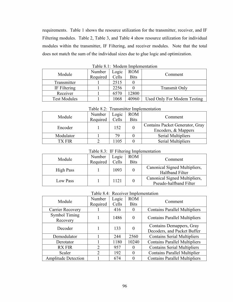
96
requirements. Table 1 shows the resource utilization for the transmitter, receiver, and IF
Filtering modules. Table 2, Table 3, and Table 4 show resource utilization for individual
modules within the transmitter, IF Filtering, and receiver modules. Note that the total
does not match the sum of the individual sizes due to glue logic and optimization.
Table 8.1: Modem Implementation
Module Number Required
Logic Cells
ROM Bits Comment
Transmitter 1 2515 0 IF Filtering 1 2256 0 Transmit Only
Receiver 1 6570 12800 Test Modules 1 1068 40960 Used Only For Modem Testing
Table 8.2: Transmitter Implementation
Module Number Required
Logic Cells
ROM Bits Comment
Encoder 1 152 0 Contains Packet Generator, Gray Encoders, & Mappers
Modulator 1 79 0 Serial Multipliers TX FIR 2 1105 0 Serial Multipliers
Table 8.3: IF Filtering Implementation
Module Number Required
Logic Cells
ROM Bits Comment
High Pass 1 1093 0 Canonical Signed Multipliers, Halfband Filter
Low Pass 1 1121 0 Canonical Signed Multipliers, Pseudo-halfband Filter
Table 8.4: Receiver Implementation
Module Number Required
Logic Cells
ROM Bits Comment
Carrier Recovery 1 416 0 Contains Parallel Multipliers Symbol Timing
Recovery 1 1486 0 Contains Parallel Multipliers
Decoder 1 133 0 Contains Demappers, Gray Decoders, and Packet Buffer
Demodulator 1 244 2560 Contains Serial Multipliers Derotator 1 1180 10240 Contains Parallel Multipliers RX FIR 2 957 0 Contains Serial Multipliers Scaler 2 192 0 Contains Parallel Multiplier
Amplitude Detection 1 674 0 Contains Parallel Multipliers

97
Enc
oder
M
odul
ator
T
X F
IR (I
Cha
nnel
)
TX
FIR
(Q C
hann
el)
Hig
h Pa
ss
Low
Pas
s
TX
Pac
ket G
ener
ator
Dem
odul
ator
R
X F
IR (I
Cha
nnel
) R
X F
IR (Q
Cha
nnel
)
Sca
ler (
I Cha
nnel
) S
cale
r (Q
Cha
nnel
)
Der
otat
or
Car
rier R
ecov
ery
Am
plitu
de D
etec
tion
Sym
bol T
imin
g R
ecov
ery
Dec
oder
Bit
Erro
r Rat
e
RX
Rot
ate
Dat
a In
R
X P
acke
t Gen
erat
or
Em
bedd
ed S
yste
m B
lock
(Use
d to
impl
emen
t RO
M)
Log
ic A
rray
Blo
ck (C
onta
ins 1
0 Lo
gic
Cel
ls)
Figure 8.4: FPGA Floor Plan of the 600,000 Gate APEX FPGA

98
The modules listed in the tables above correspond to layout constraints applied to
subsystems in the modem. The layout constraints reduce routing delays on the FPGA,
improve compile time, and maximize the FPGA area available for other uses. Each of the
large rectangles in Figure 8.4 shows the area of the FPGA where the corresponding
module was located. In general, these modules correspond to the modules in Figure 8.1,
Figure 3.2, Figure 7.8, and Figure 3.3. The exceptions are the Encoder and Decoder
meta-modules that each contains a number of smaller modules.
The Encoder and Decoder modules contain all of the logic that allows the
transmitter and receiver to deal with multiple constellations. By carefully modifying bit
shifting and burst formats within these modules, all QAM constellations are handled.
Furthermore, the design of these modules means that none of the more expensive
modules for filtering, carrier recovery, symbol timing recovery, or AGC needs to be
replicated or modified for different constellations.
The 600,000 gate APEX device contains 2432 Logic Array Blocks (LABs) and
152 Embedded System Blocks (ESBs) arranged as shown in Figure 8.4. Each LAB
contains ten logic cells that are used to implement arbitrary logic functions. Each ESB
can be configured to implement arbitrary logic functions or to act as a memory array.
In addition to the modules that implement the M-QAM modem, a number of
modules were added to the FPGA for testing and interfacing with external circuitry.
Table 8.5 shows resource utilization for modules that implement functions other than the
M-QAM modem.
Table 8.5: Test Module Implementation
Module Number Required
Logic Cells
ROM Bits Comment
Data In 1 20 0 A/D Synchronization
Packet Generator 1 105 0
Generates random data and headers for the encoder block
(Includes the TX PN Generator)
RX Packet Generator 1 22 0
Generates a time shifted copy of the data generated by the Packet
Generator block (Includes the RX PN Generator)
Bit Error Rate 1 606 0 Calculates BER and PER
RX Rotate 1 315 40960 Generates sine and cosine waves for carrier frequency offset testing

99
8.5 Bit Error Rate Results
The modem was tested using the system shown in Figure 8.1. The TX PN
Generator (implemented by the Packet Generator module) generated a pseudo-random
binary sequence that was used as input to the modem to generate 300 symbol packets.
The BER Calculator calculated the bit error rate using data from the receiver and data
from the RX PN Generator (implemented by the RX Packet Generator module), which
was synchronized to the TX PN Generator.
Each burst had a random carrier phase and a random symbol timing phase set at
the beginning of the burst. The symbol timing phase offset was adjusted to a random
setting with increments on 1/128th of a symbol digitally and the carrier phase offset was
randomly adjusted with increments of 0.09˚ digitally. In addition to the digital phase
offsets, a phase offset was present in the master clocks that drove the transmitter and
receiver that resulted in carrier and symbol timing phase offsets. In tests where a symbol
timing frequency offset was present between the transmitter and the receiver, the phase
offset between the master clocks was continuously changing.
The transmit amplifier was set to provide a signal to the receiver that was 0.5dB
above the minimum signal level allowed by the 12dB dynamic range of the modem in
order to test the worst-case performance of the modem. Section 8.9 describes the effect
of received signal amplitude on the performance of the modem and shows BER results
for the range of acceptable received signal amplitudes. This also allowed for the
minimum useful SNR to be used for testing given the limited noise power available from
the noise generation system shown in Figure 8.3.
The tests used preamble lengths of 48, 72, 96, and 144 symbols. These preamble
formats provided an indication of the sensitivity of the modem to preamble length and are
comparable to the preamble lengths used in 802.11 and 802.16 modems. 802.11 modems
use either a 72 symbol or 144 symbol Differential Binary Phase Shift Keying (DBPSK)
preamble for synchronization [45, 46]. The preamble for 802.16 modems is modulated
using a QAM-4 constellation and consists of a 32 symbol synchronization field [6, 7].
For downlink 802.16 bursts, this is followed by maps that are modulated with a QAM-4
constellation followed by a variable length section that describe the timing of upcoming
downlink and uplink bursts.

100
Figure 8.5 shows bit error rate results for the implemented modem compared to
theoretical results [31, 32, 33] and Matlab simulations of the modem for QAM-4, QAM-
16, QAM-64, and QAM-256 constellations. For BER testing, packets were transmitted
and received with the receiver synchronizing to each received packet until a statistically
significant number of bit errors were detected. Furthermore, packets with more than 50
bit errors were assumed to have suffered a synchronization error and were not used for
BER calculations.
1E-8
1E-7
1E-6
1E-5
1E-4
1E-3
1E-2
1E-1
4 6 8 10 12 14 16 18 20 22 24 26 28SNR per bit (dB)
BER
Theoretical Simulation (96 Symbol Preamble)Hardware (144 Symbol Preamble) Hardware (96 Symbol Preamble)Hardware (72 Symbol Preamble) Hardware (48 Symbol Preamble)
10-7
QAM-4
QAM-16 QAM-64 QAM-256
10-8
10-6
10-5
10-4
10-3
10-2
10-1
Figure 8.5: BER Results (Worst-case Receive Amplitude Level)
The BER curves for the implemented modem show less than 1dB of
implementation loss for all but the shortest preambles, except for the QAM-256 curve
which shows increasing implementation loss at lower BERs. At BERs of 10-6 to 10-7, the
BER performance for both QAM-4 and QAM-16 approaches the theoretical BER with 96
symbol or longer preambles. For QAM-64, there is approximately 1dB of
implementation loss at BERs of 10-6 to 10-7 with 96 symbol or longer preambles.
However, for QAM-256 there is approximately 3dB of implementation loss at a BER of
10-5 with 96 symbol or longer preambles. This suggests that the noise floor of the
modem is becoming a significant factor in the performance of the modem during QAM-
256 operation. The noise floor is a result of jitter in the synchronization loops and
truncation of both samples and filter coefficients in the modem. The effect of sample

101
truncation, described in Section 8.9, has a particularly large impact accounting for
~1.5dB of the implementation loss.
The measured BER curves show a good correlation with simulated values at
lower bit error rates. At higher BERs (lower SNR for each constellation), there is up to
1dB of implementation loss for QAM-16, QAM-64, and QAM-256. This is slightly
higher than the Matlab simulations, described in Appendix B, predicted and indicates that
there is some performance loss in the implemented synchronization loops at high BERs.
Figure 8.5 also shows the BER performance of the modem for different lengths of
preambles. For QAM-16, QAM-64, and QAM-256, the longer the preamble, the better
the BER performance. In the case of QAM-4, preamble lengths of 48 symbols to 144
symbols produced similar BER performance. Both 96 and 144 symbol preamble
sequences produced good BER performance for all constellations. Excluding QAM-4
constellations, preambles with 72 symbols produced BER performance that was slightly
degraded at low BERs. For 48 symbol preambles, BER performance was significantly
degraded for all but QAM-4 constellations.
8.6 Packet Error Rate
Packet Error Rate, PER, is used to measure the ability of the modem to correctly
synchronize with the received burst. Packet errors can be categorized into three groups
for the implemented modem:
• packets that are not detected,
• packets that are detected when no packet is received, and
• packets that are detected correctly but experience large numbers of bit errors due to
failures of the synchronization loops to adequately track amplitude, carrier phase, or
symbol timing variations.
The failure to detect a packet is detected by the BER Calculator module on the
FPGA that implements the modem. The BER calculator receives information from both
the receiver and the RX packet generator. Since the RX Packet Generator is triggered by
the data source for the transmitter, the signals from the RX Packet Generator can be used
to determine when each packet is sent. Thus by counting the number of packets sent and
the number of packets received, the PER due to missed packets can be calculated.

102
Figure 8.6 shows the PER due to bursts that are not detected as a function of SNR
for preamble lengths of 48, 72, 96, and 144 symbols. PER due to missed packet detection
is independent of constellation since the synchronization sequence consists of the four
outside constellation points repeated in the same sequence for all constellations. From
the curves, it can be seen that the PER due to missed packets approaches a constant value
that is dependent on the preamble length as the SNR increases. Figure 8.6 also shows
that the PER due to undetected packets at a given SNR is dependent on the length of the
preamble with longer preambles having a lower chance of not detecting a burst.
1E-7
1E-6
1E-5
1E-4
1E-3
1E-2
1E-1
1E+0
4 6 8 10 12 14 16 18 20 22 24 26 28 30 32 34 36Preamble SNR per bit (dB)
PER
(Und
etec
ted
Pack
ets)
Hardware (144 Symbol Preamble) Hardware (96 Symbol Preamble)Hardware (72 Symbol Preamble) Hardware (48 Symbol Preamble)
10-6
10-7
10-5
10-4
10-3
10-2
10-1
10-0
Figure 8.6: PER Results (Undetected Packets)
Since the PER due to undetected packets was independent of constellation, the
PER due to undetected bursts was plotted with respect to preamble SNR per bit. All
other results were plotted with respect to data segment SNR per bit since most results are
dependent on the data segment SNR per bit. The relationship between data segment SNR
per bit and preamble SNR per bit is dependent on the modem and the number of bits per
symbol. Data segment SNR per bit for the implemented modem can be determined by
subtracting 0dB, 5.6dB, 9.0dB, or 10.3dB from the preamble SNR per bit for QAM-4, 16,
64 or 256 operation respectively.
For a detected packet, a packet error is assumed to be a burst with more than 50
bit errors. More than 50 bit errors in a 300 symbol packet could be a result of three

103
causes: the detection of a burst where no burst is present, a catastrophic synchronization
failure, or an accumulation of bit errors due to noise.
The detection of a packet where none is present, a framing error, is a significant
source of packet errors when the modem is operating at low SNRs. The process for the
modem to detect a packet of data consists of three steps. First, the modem detects the
preamble by the presence of six consecutive preamble symbols in the correct order.
Secondly, the modem verifies that a minimum preamble length (32 symbols for testing)
has been reached to reduce the probability of the modem detecting a preamble when none
is present. Finally, the modem detects the end of the preamble by an End Of Preamble
symbol that occurs two symbols before the data segment of the burst begins.
The most likely cause of a framing error is a bit error that causes a preamble
symbol to appear to be the End Of Preamble symbol after the minimum preamble length
has been reached. Figure 8.7 shows simulated and measured PER for detected packets
for a QAM-4 signal. Figure 8.7 also shows theoretical PER plots for burst detection that
result from framing errors caused by bit errors during the preamble that occur after the
minimum preamble length has been reached but before the actual End Of Preamble
symbol. Comparing the theoretical PER curves to the measured PER curves, it can be
seen that for SNRs less than 10dB per bit, packet errors are dominated by framing errors.
1E-6
1E-5
1E-4
1E-3
1E-2
1E-1
1E+0
2 4 6 8 10 12Preamble SNR per bit (dB)
PER
(Det
ecte
d Pa
cket
s) .
Simulation (96 Symbol Preamble) Theoretical (48 Symbol Preamble)Theoretical (144 Symbol Preamble) Hardware (48 Symbol Preamble)Hardware (72 Symbol Preamble) Hardware (96 Symbol Preamble)Hardware (144 Symbol Preamble)
10-6
10-5
10-4
10-3
10-2
10-1
10-0
Figure 8.7: PER Results for Detected QAM-4 Packets

104
The behavior of framing errors is the same in all constellations since all
constellations use the same preamble sequence. However, framing errors drop rapidly as
the SNR increases. Therefore, framing errors have very little impact on higher order
QAM constellations that are typically only used at higher SNRs.
The other significant result present in Figure 8.7 is that the PER increases with
increasing preamble length when framing errors are the dominant source of packet errors.
The increase in PER as a function of preamble length is due to the increased probability
of a bit error occurring between when the receiver has counted the 32nd preamble symbol
and the actual End of Preamble symbol.
Figure 8.8 shows that PER varies strongly as a function of preamble length for
QAM-16, QAM-64 and QAM-256. This effect was not seen for QAM-4 in Figure 8.7
because framing errors dominated over other packet error sources. For QAM-16, QAM-
64, and QAM-256, PER improves as the length of the preamble increases. The
dependence on preamble length is due to the receiver generating better estimates in each
of the synchronization loops during longer preambles. Furthermore, since a different
minimum level of synchronization is required for each constellation, the PER levels for
each preamble length are different for each constellation.
1E-7
1E-6
1E-5
1E-4
1E-3
1E-2
1E-1
1E+0
4 6 8 10 12 14 16 18 20 22 24 26 28Data Segment SNR per bit (dB)
PER
(Det
ecte
d Pa
cket
s)
Hardware (144 Symbol Preamble) Hardware (96 Symbol Preamble)Hardware (72 Symbol Preamble) Hardware (48 Symbol Preamble)
10-6
10-7
10-5
10-4
10-3
10-2
10-1
10-0
QAM-16
QAM-64 QAM-256
Figure 8.8: PER Results for Detected QAM-16, QAM-64 and QAM-256 Bursts

105
Comparing Figure 8.8 with Figure 8.5 shows that the PER for QAM-64 and 256 is
relatively constant with respect to SNR at SNRs large enough to produce BERs below
1×10⁻². The PER in this case is due to random synchronization errors and seems
somewhat independent of random bit errors. This is seen in the curves with preambles
equal to 48, 72 and 96 symbols. For the curves with preamble length equal to 144
symbols, the PER became too low to measure with the current test setup but the PER
curves would be expected to have a similar shape as the PER curves for other preamble
lengths. The PER curves for QAM-16 show a similar shape to the QAM-64 and
QAM-256 curves; however, the transition to a constant PER is more gradual. At low
SNRs where the BER is above 1×10⁻², the PER rises sharply in all three cases as the
synchronization loops can no longer average out the noise due to bursts of bit errors and
as bursts begin to incur more than 50 bit errors due to noise.
The total PER for the modem is the sum of the PER for undetected packets and
the PER for detected packets. For QAM-4 packets, where framing errors dominate the
PER for detected packets, the total packet error rate is the sum of the PERs shown in
Figure 8.6 and Figure 8.7. For QAM-16, QAM-64 and QAM-256, the total packet error
rate is the sum of the PERs shown in Figure 8.6 and Figure 8.8. In this case, either the
preamble SNR must be converted to data segment SNR or vice versa before summing the
PERs.
8.7 Effect of Carrier Frequency Offsets on BER
The receiver demodulates a QAM signal by first undersampling the signal at IF to
obtain a baseband signal centred at a frequency equal to the symbol rate and then
multiplying the baseband signal by sine and cosine waves to obtain the in-phase and
quadrature components. The effect of a carrier frequency offset between the
undersampled signal and the demodulating waveforms was tested by changing the
frequency of the sine and cosine waves generated in the receiver.
The frequency of the sine and cosine waves was controlled by digital inputs to the
modem that, in turn, control a counter in a Numerically Controlled Oscillator (NCO) with
a 4096 entry lookup table. By manipulating the inputs, carrier frequency offsets of 0,
0.002%, 0.004%, or 0.008% of the symbol rate can be generated for carrier frequency

106
offset testing. The 0.008% offset is larger than the typical frequency variation of
0.0002% to 0.005% for a crystal oscillator that would be used to generate the master
clock for the modem. However, the master clock accuracy affects the undersampling
operation resulting in additional frequency offsets. Additionally, upconversion and
downconversion stages can introduce carrier frequency offset into the received signal.
Therefore, depending on the accuracy of the crystal oscillator used, the amount of
undersampling, and the amount of up/downconversion, the frequency range of the carrier
recovery system may need to be expanded.
The modem generates an estimate of the carrier frequency offset during the
preamble and tracks the carrier offset throughout the burst. The quality of the carrier
frequency offset estimate at the beginning of the data segment is dependent on the length
of the preamble and the size of the carrier frequency offset. Larger carrier frequency
offsets take longer for the second order tracking loop to synchronize with. However, the
tracking loop continues to synchronize during the data segment of the burst so
synchronization will continue even if a good estimate was not generated by the end of the
preamble.
The plots in Figure 8.9 show the BER effect of an offset in carrier frequencies
between the transmitter and the receiver for each constellation and for the four tested
preamble lengths. The SNR for each plot was chosen such that the BER with no
frequency offset would be approximately 1×10⁻⁴ to 1×10⁻⁵. Additionally, the SNR for
each curve is approximate as the sequence of testing was to first measure the effects of
carrier offsets for each constellation using 144 symbol preambles. The testing was then
repeated with 96, 72, and 48 symbol preambles.
The plots show that the BER increases as the carrier frequency offset increases.
As well, the plots show that the shorter the preamble, the greater the increase in BER as
the frequency offset is increased. This indicates that a better estimate of the carrier
frequency offset is generated before the end of the preamble when longer preambles are
used.
Additional testing in Section 8.10 indicates that the majority of the bit errors
occur near the beginning of the packet. This information on the distribution of bit errors
indicates that the carrier frequency estimate is improved throughout the data segment.

107
1E-5
1E-4
1E-3
1E-2
0.E+00 2.E-05 4.E-05 6.E-05 8.E-05
Carrier Offset
BER
-QA
M-2
56
10-5
10-4
10-3
10-2
0×10-5 4×10⁻⁵ 8×10⁻⁵
SNR/bit=23.3dB1E-5
1E-4
1E-3
1E-2
0.E+00 2.E-05 4.E-05 6.E-05 8.E-05
Carrier Offset
BER
QA
M-6
4
10-5
10-4
10-3
10-2
0×10-5 4×10⁻⁵ 8×10⁻⁵
SNR/bit=17.6dB
1E-5
1E-4
1E-3
1E-2
0.E+00 2.E-05 4.E-05 6.E-05 8.E-05
Carrier Offset
BER
QA
M-1
6
10-5
10-4
10-3
10-2
0×10-5 4×10⁻⁵ 8×10⁻⁵
SNR/bit=13.1dB
1E-5
1E-4
1E-3
1E-2
0.E+00 2.E-05 4.E-05 6.E-05 8.E-05
Carrier OffsetB
ER Q
AM
-4
10-5
10-4
10-3
10-2
0×10-5 4×10⁻⁵ 8×10⁻⁵
SNR/bit=9.7dB
Figure 8.9: Effect of Carrier Offset on BER
The plots in Figure 8.10 show that a carrier frequency offset has a similar effect
on PER as on BER. The plots show that the PER increases as the carrier frequency offset
increases in all cases except QAM-4 where the PER is dominated by framing errors. Not
all preamble lengths are shown for each constellation because the PERs for some
preamble lengths fell below what was measurable for the current test system. As well,
the SNR for each curve is approximate since the measurements were taken in the same
sequence as the BER measurements.
Figure 8.9 and Figure 8.10 indicate that the implemented carrier recovery system
can effectively detect and track carrier frequency offsets. The effect of the frequency
offset is small on both BER and PER. However, for carrier frequency offsets larger than
shown in Figure 8.9 and Figure 8.10, longer preambles or modifications to the carrier
recovery system may be necessary depending on the required level of performance.
(a) (b)
(c) (d) 144 Symbol Preamble96 Symbol Preamble
y72 Symbol Preamble48 Symbol Preamble

108
1E-6
1E-5
1E-4
1E-3
1E-2
1E-1
1E+0
0.E+00 2.E-05 4.E-05 6.E-05 8.E-05
Carrier Offset
PER
-QA
M-2
56
0×10-5 4×10⁻⁵ 8×10-510-6
10-4
10-2
100
SNR/bit=23.3dB1E-6
1E-5
1E-4
1E-3
1E-2
1E-1
1E+0
0.E+00 2.E-05 4.E-05 6.E-05 8.E-05
Carrier Offset
PER
-QA
M-6
4
0×10-5 4×10⁻⁵ 8×10-510-6
10-4
10-2
100
SNR/bit=17.6dB
1E-6
1E-5
1E-4
1E-3
1E-2
1E-1
1E+0
0.E+00 2.E-05 4.E-05 6.E-05 8.E-05
Carrier Offset
PER
-QA
M-1
6
0×10-5 4×10⁻⁵ 8×10-510-6
10-4
10-2
100
SNR/bit=13.1dB
1E-6
1E-5
1E-4
1E-3
1E-2
1E-1
1E+0
0.E+00 2.E-05 4.E-05 6.E-05 8.E-05
Carrier OffsetPE
R-Q
AM
-40×10-5 4×10⁻⁵ 8×10⁻⁵
10-6
10-4
10-2
100
SNR/bit=9.7dB
Figure 8.10: Effect of Carrier Offset on PER
8.8 Effect of Symbol Timing Frequency Offsets on BER
The effect of a symbol timing frequency offset was tested by introducing a
symbol timing frequency offset between the transmitter and the receiver. Separate
clocks, each generated by a signal generator and fed into the FPGA via separate clock
busses, were used for the transmitter and receiver allowing the transmitter and receiver to
run at different frequencies for testing. Since the symbol rate is proportional to the
frequency of the master clocks, changing the receiver’s master clock frequency allows the
receiver symbol clock to be varied in order to generate a symbol timing frequency offset.
Changing the master clock in the receiver also generates carrier frequency offsets.
The first source of carrier frequency offsets is from undersampling based on a master
clock different than was used for upsampling in the transmitter. The second source of
carrier frequency offsets is from the sine and cosine waves used to demodulate the
received signal that are a different frequency than the sine and cosine waves used to
modulate the signal. The sine and cosine waves are a different frequency because they
are generated from a different master clock than was used in the transmitter. These
(a) (b)
(c) (d) 144 Symbol Preamble96 Symbol Preamble
y72 Symbol Preamble48 Symbol Preamble

109
frequency offsets were compensated using the same technique that was described in
Section 8.7 to generate a carrier frequency offset. Additionally, master clock increments
were chosen that allowed the resulting carrier frequency offsets to be matched exactly.
Symbol timing frequency offsets of 0, 0.02%, or 0.04% of the symbol rate were
generated for carrier frequency offset testing. The 0.04% offset is considerably larger
than the typical frequency variation of 0.0002% to 0.005% for a crystal oscillator that
would be used to generate the master clock for the modem. Thus, the testing should
provide a good indication of the performance of the symbol timing recovery system.
The plots in Figure 8.11 show the BER effect of an offset in symbol timing
frequencies between the transmitter and the receiver for each constellation and for the
four tested preamble lengths as a function of the symbol timing offset per symbol. The
SNR for each plot was chosen such that the BER with no frequency offset would be
approximately 1×10⁻⁴ to 1×10⁻⁵. Additionally, the SNR for each curve is approximate as
the sequence of testing was to measure the effects of carrier offsets for each constellation
using 144 symbol preambles. The testing was then repeated with 96, 72, and 48 symbol
preambles using approximately the same SNR.
1E-5
1E-4
1E-3
1E-2
0.E+00 6.E-04 1.E-03
Symbol Timing Offset
BER
-QA
M-2
56
10-5
10-4
10-3
10-2
0×10-4 2×10⁻⁴ 4×10⁻⁴
SNR/bit=23.3dB1E-5
1E-4
1E-3
1E-2
0.E+00 6.E-04 1.E-03
Symbol Timing Offset
BER
-QA
M-6
4
10-5
10-4
10-3
10-2
0×10-4 2×10⁻⁴ 4×10⁻⁴
SNR/bit=17.6dB
1E-5
1E-4
1E-3
1E-2
0.E+00 6.E-04 1.E-03
Symbol Timing Offset
BER
-QA
M-1
6
10-5
10-4
10-3
10-2
0×10-4 2×10⁻⁴ 4×10⁻⁴
SNR/bit=13.1dB
1E-5
1E-4
1E-3
1E-2
0.E+00 6.E-04 1.E-03
Symbol Timing Offset
BER
-QA
M-4
10-5
10-4
10-3
10-2
0×10-4 2×10⁻⁴ 4×10⁻⁴
SNR/bit=9.7dB
Figure 8.11: Effect of Symbol Timing Frequency Offset on BER
(a) (b)
(c) (d) 144 Symbol Preamble96 Symbol Preamble
y72 Symbol Preamble48 Symbol Preamble
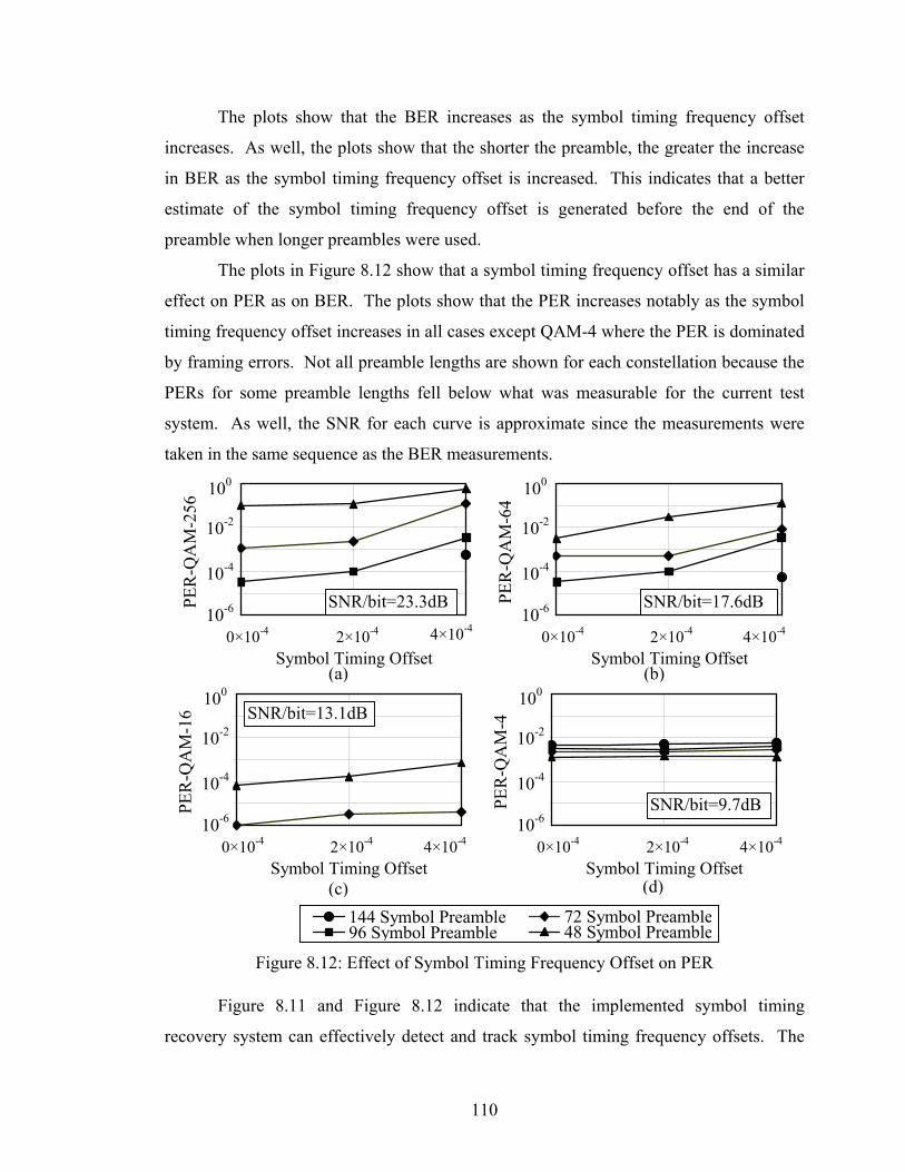
110
The plots show that the BER increases as the symbol timing frequency offset
increases. As well, the plots show that the shorter the preamble, the greater the increase
in BER as the symbol timing frequency offset is increased. This indicates that a better
estimate of the symbol timing frequency offset is generated before the end of the
preamble when longer preambles were used.
The plots in Figure 8.12 show that a symbol timing frequency offset has a similar
effect on PER as on BER. The plots show that the PER increases notably as the symbol
timing frequency offset increases in all cases except QAM-4 where the PER is dominated
by framing errors. Not all preamble lengths are shown for each constellation because the
PERs for some preamble lengths fell below what was measurable for the current test
system. As well, the SNR for each curve is approximate since the measurements were
taken in the same sequence as the BER measurements.
1E-6
1E-5
1E-4
1E-3
1E-2
1E-1
1E+0
0.E+00 6.E-04 1.E-03
Symbol Timing Offset
PER
-QA
M-2
56
0×10-4 2×10⁻⁴ 4×10-410-6
10-4
10-2
100
SNR/bit=23.3dB1E-6
1E-5
1E-4
1E-3
1E-2
1E-1
1E+0
0.E+00 6.E-04 1.E-03
Symbol Timing Offset
PER
-QA
M-6
4
0×10-4 2×10⁻⁴ 4×10-410-6
10-4
10-2
100
SNR/bit=17.6dB
1E-6
1E-5
1E-4
1E-3
1E-2
1E-1
1E+0
0.E+00 6.E-04 1.E-03
Symbol Timing Offset
PER
-QA
M-1
6
0×10-4 2×10⁻⁴ 4×10-410-6
10-4
10-2
100
SNR/bit=13.1dB
1E-6
1E-5
1E-4
1E-3
1E-2
1E-1
1E+0
0.E+00 6.E-04 1.E-03
Symbol Timing Offset
PER
-QA
M-4
0×10-4 2×10⁻⁴ 4×10-410-6
10-4
10-2
100
SNR/bit=9.7dB
Figure 8.12: Effect of Symbol Timing Frequency Offset on PER
Figure 8.11 and Figure 8.12 indicate that the implemented symbol timing
recovery system can effectively detect and track symbol timing frequency offsets. The
(a) (b)
(c) (d)
144 Symbol Preamble96 Symbol Preamble
y72 Symbol Preamble48 Symbol Preamble

111
effect of the frequency offset is acceptable for both BER and PER over the expected
range of frequency offsets for normal operation.
8.9 Effect of Amplitude Variation on BER
The amplitude of the received signal has an impact on the performance of the
modem because the A/D converter that samples the received signal uses a fixed number
of bits to represent each sample. The modem uses 10-bit samples from an A/D converter
and is designed to work over a 12dB range of input signals. As the peak-to-peak signal
level decreases from the maximum allowed signal to the minimum allowed signal, the
effective resolution decreases from 1/210 to 1/28.
The BER and PER testing in Sections 8.5 to 8.8 were performed with the transmit
amplifier set to provide a signal to the receiver that was 0.5dB above the minimum signal
level allowed for by the 12dB dynamic range of the modem in order to test the worst-case
performance of the modem. However, to evaluate the effect that the received signal level
had on modem performance, the received signal level was changed by passing it through
a variable attenuator and by changing the gain of the transmit amplifier. Changing only
the attenuation of the variable attenuator allowed the effects of different received signal
levels to be studied. Changing the gain of the amplifier allowed measurements to
determine if amplifier distortion was affecting the BER.
Figure 8.13, Figure 8.14, and Figure 8.15 show the effect of increased effective
A/D resolution for QAM-256, QAM-64, and QAM-16 respectively at three different
amplifier settings. Each plot shows BER results over the 12dB range of amplitudes the
receiver is designed to accommodate and are generated with a 144 symbol preamble. The
effect of amplitude variation could not be simulated for QAM-4 since the current test
setup could not generate enough noise to obtain a measurable BER if the signal power is
increased. The plots indicate that the BER decreases as the effective resolution is
increased. The plots also show that the rate at which the BER decreases becomes greater
as M becomes larger. Figure 8.13 shows that the BER decreased by 2.6 times as the
amplitude of the received signal was increased for QAM-256 with an 11dB amplifier
setting. Less change is seen for QAM-64 in Figure 8.14 and almost no change is seen for
QAM-16 in Figure 8.15. This increased impact of effective resolution on larger

112
1E-5
1E-4
1E-3
0.0 2.0 4.0 6.0 8.0 10.0 12.0Level Relative to Minimum Input Level (dB)
BER
- Q
AM
256
Gain = 0dB Gain = 6dB Gain = 11dB
10-5
10-4
10-3
SNR/bit=24.2dB
Figure 8.13: Effect of Amplitude Variation on QAM-256 BER
1E-5
1E-4
1E-3
0.0 2.0 4.0 6.0 8.0 10.0 12.0Level Relative to Minimum Input Level (dB)
BER
- Q
AM
64
Gain = 0dB Gain = 6dB Gain = 11dB
10-5
10-4
10-3
SNR/bit=17.5dB
Figure 8.14: Effect of Amplitude Variation on QAM-64 BER
1E-5
1E-4
1E-3
0.0 2.0 4.0 6.0 8.0 10.0 12.0Level Relative to Minimum Input Level (dB)
BER
- Q
AM
16
Gain = 0dB Gain = 6dB Gain = 11dB
10-5
10-4
10-3
SNR/bit=12dB
Figure 8.15: Effect of Amplitude Variation on QAM-16 BER

113
constellations is consistent with the constellation points being closer together in the larger
constellations.
Figure 8.13, Figure 8.14, and Figure 8.15 also show that the transmit amplifier
causes an increase in BER as the gain is increased when a corresponding increase in
attenuation offsets the gain. No significant change in BER results at a given signal level
when increasing the amplifier gain from 0dB to 6dB but BER increases noticeably when
the amplifier gain is increased from 6dB to 11dB. This is due to distortion resulting from
increasing the amplifier gain. For QAM 256 operation, the BER increases by 2.75 times
when the amplifier gain is increased from 6dB to 11dB while QAM-64 operation shows
less degradation and QAM-16 operation shows almost no change. This increased impact
on the larger constellation is consistent with the constellation points being closer together
in the larger constellations. In addition, at 11dB gain, the amplifier distortion tends to
dominate over the resolution at high effective resolutions resulting in a minimum BER
level for QAM-256 and QAM-64 operation. As a result, the modem cannot perform at
the maximum possible performance using the current test system.
The BER performance in the absence of amplifier distortion can be inferred by the
slopes of the BER curves in Figure 8.13, Figure 8.14, and Figure 8.15. The dashed lines
in Figure 8.13 and Figure 8.14 show BER as a function of amplitude if amplifier
distortion is ignored. No extrapolation is needed in Figure 8.15 since amplifier distortion
does not significantly affect performance. Using the inferred BER performance shown
by the dashed lines in Figure 8.13, Figure 8.14, and Figure 8.15, implementation loss for
QAM-256 operation at an SNR per bit of 24.2dB is expected to drop from 3dB at the
minimum signal level to 1.5 dB at the maximum signal level unless another source of
error begins to dominate. Similarly, implementation loss for QAM-64 operation at an
SNR per bit of 17.5dB is expected to drop from 1dB at the minimum signal level to 0.5
dB at the maximum signal level.
Due to the limited number of bits in the A/D conversion that limit AGC range, the
modem can only operate in environments with signal variability that is less than 12dB.
An external amplifier or attenuator controlled by the AGC would be required for
environments where more than 12dB of fading occurs. The “coarse” external AGC
amplifier or attenuator could operate throughout each burst or only at the beginning of

114
each burst and rely on the “fine” internal AGC to compensate for amplitude variation
during the burst.
In the case where the external AGC operates only at the beginning of the burst,
burst lengths would have to be limited to a period of time where less than ±6dB variation
would occur in signal level for the current modem implementation that uses a 10-bit A/D
and a 12dB internal AGC range. In the case where the external AGC operates throughout
the burst, the external gain could be changed to any value between the minimum and
maximum gain values or one of a number of discrete gain settings. A good technique
would be to use discrete gain settings that result in signal amplitudes that double from
one setting to the next since the RRC filters in the receiver can be easily modified to
multiply all stored amplitude values inside the filter by either one half or two. By
multiplying the values inside the filter to match changes in external gain, no step
discontinuities in amplitude occur within the RRC filters.
8.10 Effect of Packet Length on BER
The modem implemented for testing does not allow the length of the burst to be
varied. However, the effect of burst length on BER can be inferred by looking at the
distribution of errors throughout the packet. Figure 8.16, Figure 8.17, and Figure 8.19
show the distribution of bit errors throughout a burst as a function of time. Each plot is
generated with 65353 bit errors and normalized by BER. The three plots were generated
during QAM-256 operation and were similar to results for other constellations.
Figure 8.16 shows that the distribution of bit errors is constant throughout the
burst when both the carrier frequency and the symbol timing frequency of the receiver are
the same as the transmitter.
0.50.75
11.251.5
1.75
0 50 100 150 200 250 300Symbol
Rel
ativ
e B
ER
Figure 8.16: Distribution of Bit Errors

115
Figure 8.17 shows that the distribution of bit errors is not constant throughout the
burst when there is a 0.008% offset in carrier frequency between the transmitter and the
receiver. The BER initially climbs to ~2.2 times the BER when no carrier frequency
offset is present before falling to the same BER as when no carrier frequency offset is
present. The BER rate then remains stable from ~170 symbols onward. The higher BER
during the first half of the burst is due to the second-order carrier recovery not yet having
a good estimate of the carrier frequency offset.
0
1
2
3
0 50 100 150 200 250 300Symbol
Rel
ativ
e B
ER
Figure 8.17: Distribution of Bit Errors (Carrier Frequency Offset)
The initial rise in BER during the first 30 symbols is due to decreased average
symbol amplitude during the data segment (shown in Figure 8.18b) of the burst compared
to the constant symbol amplitude during the preamble (shown in Figure 8.18a). The
phase detector for the carrier recovery system calculates the phase error based on
Equation 6.11 where the output of the phase detector is dependent on the distance
between ( )QI ′′, , shown by the solid circles in Figure 8.18, and ( )QI ˆ,ˆ , shown by the
unfilled circles. Since the average symbol amplitude is reduced in the data segment
relative to the preamble, the output of the phase detector is also reduced relative to the
phase error resulting in a smaller feedback signal relative to the phase error. Therefore,
static error in the first-order segment of the carrier recovery loop, which is inversely
proportional to the feedback signal, increases by an amount proportional to the decrease
in the average symbol amplitude. This increase in static error produces an increase in
BER until the second order segment of the loop fully synchronizes with the carrier
frequency offset.

116
5
5
15
15 (I´, Q´)
(a) (b)
Φ
5
5
15
15
(I´, Q´)
Φ
10
1010
10
(I, Q)
(I, Q)
Figure 8.18: Carrier Recovery Gain Differences
Figure 8.19 shows that the distribution of bit errors is not constant throughout the
burst when there is a 0.04% offset in symbol timing frequency between the transmitter
and the receiver. The BER is initially ~2.6 times the BER when no symbol timing
frequency offset is present before falling to ~1.4 times the BER when no symbol timing
frequency offset is present. The BER then remains stable from ~180 symbols onward.
The higher BER during the first half of the burst is due to the second-order symbol timing
recovery not yet having a good estimate of the symbol timing frequency offset. The
increased BER at the end of the burst is probably due to ISI caused by a relative symbol
timing offset between the first and last symbols in the RX FIR filters since there is
approximately 0.003 symbol offset across the filters which use samples spanning eight
symbol periods.
1
2
3
4
0 50 100 150 200 250 300Symbol
Rel
ativ
e B
ER
Figure 8.19: Distribution of Bit Errors (Symbol Timing Frequency Offset)

117
The constant BER profile of Figure 8.16 indicates that the BER is independent of
burst length when no carrier frequency offsets or symbol timing frequency offsets are
present between the transmitter and the receiver. The BER profiles in Figure 8.17 and
Figure 8.19 show that when either carrier frequency or symbol timing frequency offsets
are present, the BER will be increased until the second order tracking loops have
accurately estimated the frequency offsets. Therefore, BER actually decreases as a
function of packet length when a carrier frequency or symbol timing frequency offset is
present.

118
Chapter 9
Summary and Conclusions
9.1 Summary of Objectives
The goal of this research was to develop and test an adaptive M-QAM modem
hardware architecture suitable for use as a modem core for programmable software
defined radios (SDRs) and broadband wireless applications where the SNR can vary over
a wide range. To meet this goal, four objectives were identified and executed.
The first objective was to develop a modem architecture with burst mode
capabilities such that each burst could be received independently of all other bursts in
order to allow the modem to operate in TDM or TDD mode. This development resulted
in an architecture that allowed each burst to be modulated with a constellation that was
most appropriate for the channel conditions between the source and destination at the
point in time when the burst was transmitted. Chapters 1 and 2 provided information on
previous work and modem theory. Chapter 3 detailed the modem architecture that was
developed and Chapter 7 described the architecture for the required filters.
The second objective was to research, implement, and test synchronization
methods that would be appropriate for use with multiple QAM constellations over a wide
range of SNRs. The carrier, clock, amplitude, frame, and modulation level
synchronization functions that were implemented operated reliably without prior
knowledge of the QAM modulation level used in the burst. The synchronization
functions operated quickly to synchronize with the received packet during a short
preamble and to track the synchronization parameters throughout the data segment of the
burst. Furthermore, the receiver was able to synchronize to a high percentage of bursts
and the synchronization loops maintained a high level of synchronization over a wide
119
range of SNRs. Chapters 4 through 6 described the AGC, symbol timing, and carrier
recovery systems in detail.
The AGC and carrier recovery systems used a simple modulus operation that was
efficiently implemented in hardware to facilitate operation with multiple constellations.
The symbol timing recovery system used a novel predicted edge crossing technique
developed by the author. The predicted edge crossing symbol timing recovery system
was derived from the zero-crossing technique for symbol timing recovery but was
modified to allow operation with high-order QAM constellations. The predicted edge
crossing technique had the added benefit that, with very compact prediction filters, it
could effectively cancel out ISI effects that cause jitter in the zero-crossing symbol timing
recovery technique.
The third objective was to exploit commonality in the M-QAM constellations to
minimize the redundant hardware required. The commonality in the different QAM
constellations was to be used to allow multiple subsystems to operate on multiple
constellations without modifying their operation or duplicating modules. The
implemented architecture utilized a unique bit stuffing and shifting architecture that
allowed most modem subsystems to operate without knowledge of the constellation being
transmitted or received. Chapter 3 described how the modem architecture facilitated
operation on multiple constellations. Chapters 4 through 6 detailed how the
synchronization functions dealt with multiple constellations during the data segment of
each burst.
The fourth objective was to compare the performance of the modem to theoretical
performance limits using a simulated radio channel. Chapter 8 described both hardware
implementation and performance results for the modem. The implementation results
described the implementation of both the modem and related testing modules in a
moderately sized FGPA. The performance results for the implemented system in the
presence of noise were compared to numerical simulation and theory. Furthermore, the
performance of the modem was characterized for common operating impairments such as
carrier and symbol timing frequency offsets.

120
9.2 Summary of Results and Conclusion
The architecture described in this thesis illustrated how a burst-mode M-QAM
modem could be designed to adapt to a varying constellation size on a burst-by-burst
basis. The architecture relied on the inherent similarities between different QAM
constellations to process all constellations with a common hardware configuration. The
architecture effectively dealt with the changing number of bits per symbol and directly
supported variable bit rate operation.
This modem was especially suitable for programmable logic implementation. A
complete adaptive, burst mode M-QAM modem designed to handle bit rates from 2 to 8
Mb/s with a maximum constellation size of 256 symbols was be effectively implemented
in a moderately sized FPGA.
The modem BER performance approached theoretical levels for QAM-4 and
QAM-16 while it experienced up to 1dB of performance degradation during QAM-64
operation and 1dB to 4dB performance degradation during QAM-256 operation
depending on the received signal level and the SNR. The modem experienced acceptable
burst synchronization performance for each mode of operation with the best burst
synchronization occurring at high SNRs.
The modem performed well when subjected to both carrier frequency and symbol
timing frequency offsets. The carrier recovery system showed good synchronization with
frequency variation up to 0.008% of the symbol rate, which was larger than the typical
frequency variation of 0.0002% to 0.005% for a crystal oscillator. However, depending
on the accuracy of upconversion and downconversion as well as the desired performance
levels, the range of the carrier recovery system may need to be expanded. The symbol
timing recovery system showed excellent synchronization up to 0.04% of the symbol rate
which was considerably larger than the typical frequency variation of 0.0002% to 0.005%
for a crystal oscillator that would be used to generate the master clock for the modem.
The modem used bursts that are 300 symbols long. Tests indicated the modem
would be capable of supporting variable burst lengths ranging from much shorter to much
longer than the current 300 symbol bursts without a significant difference in BER
performance. In particular, when carrier or symbol timing frequency offsets were
present, testing indicated that the performance of the modem would actually improve

121
with increasing packet length.
Tests on the effects of received signal amplitude indicated that the receiver could
handle varying signal levels. However, a controllable external amplifier or attenuator
would be required to use the modem in environments where large amplitude variation due
to deep fading is present.
9.3 Recommendations for Future Study
The research for this thesis uncovered a number of avenues for further study.
These prospects for study include
• the use of different preambles,
• the effects of bursts that contain multiple segments with different values of M,
• the feasibility of using digital upconversion to a standard IF frequency,
• the use of dedicated hardware multipliers,
• the effects of using an external amplifier or attenuator to extend the AGC range, and
• the measurement of the current channel integrity to predict the optimal constellation
to maximize throughput.
The effects of using different preamble sequences would be a valid area of study.
The preamble used was a +1, -1, -1, +1 sequence that provided many zero crossing
transitions that aided synchronization. However, the sequence produced spikes in the
frequency domain due to its repetitiveness. Depending on the channel and the spectrum
regulations, a synchronization sequence with a flatter spectrum may be advantageous.
Therefore, it would be valuable to evaluate the synchronization performance of this
modem with standard preamble sequences such as those used by 802.11 or 802.16.
The effects of using different constellations within a single burst should be
investigated. Modern modem technologies such as 802.16 are employing multiple
constellations within a burst to serve multiple receivers, each of which faces different
channel conditions, with a single transmission. However, this technique also has
advantages for synchronization because different constellations require different levels of
synchronization. By placing different constellations within a burst, starting with the
simplest constellation at the beginning of the burst, more complex constellations near the
end of the burst can take advantage of the tracking features of the synchronization loops
122
to provide improved estimates for each synchronization parameter.
Investigating the complexity of using digital up-conversion to move the
transmitted spectrum up to a standard Intermediate Frequency (IF) such as 45MHz or
70MHz would be worthwhile. Early experiments indicated that this would be easily
accomplished since the FPGA used was able to generate waveforms at those frequencies
and Surface Acoustic Wave (SAW) filters are readily available to replace the
reconstruction filters currently used.
The impact of using hardware multipliers and other filter structures should be
investigated. The use of serial filters for the RRC filters saved significant space but the
rate at which the serial filters could be operated was significantly lower than expected.
This resulted in a lower symbol rate than would otherwise be possible. The use of serial
filters also added complexity since multiple clock domains were required so that serial
logic in the filters could be clocked faster than the rest of the logic in the modem. The
use of hardware multipliers could resolve both the space problems associated with using
hardware multipliers and the speed problems associated with using serial multipliers for
filters.
The complexity and cost of using a controllable external gain source to extend the
AGC range should be investigated. Section 8.9 described several options for
implementing an external amplifier or attenuator that could be controlled by the current
AGC hardware. From a preliminary analysis, the implementation complexity appeared to
be low but there may be some impacts on the synchronization functions and the RX FIR
filter structure due to highly variable signal levels before AGC synchronization has
occurred.
Techniques for the measurement of the current channel integrity should be
evaluated as a means to predict the optimal constellation to maximize throughput. The
channel integrity can be estimated using either measured BER or the received SNR.
Using SNR appears more promising than BER since a large number of symbols are
required to obtain a statistically significant BER. In practice, the SNR could be estimated
from the average signal level and the Error Vector Magnitude (EVM), which is the
distance from the actual location of the received symbol in the vector signal space to the
ideal location of the received symbol in the vector signal space.

123
References
[1] A. J.Viterbi, “The Evolution of Digital Wireless Technology from Space Exploration
to Personal Communication Services,” IEEE Transactions on Vehicular Technology, vol. 43, no. 3, pp. 638-641, August 1994.
[2] G. Young, The Internet, The H. W. Wilson Company, New York, NY, 1998.
[3] M. Honda et al., “Efficient Configuration Data Transmission Scheme for FPGA-Based Downloadable Software Radio Communication System,” IEEE 54th Vehicular Technology Conference (VTC Fall 2001), vol. 3, pp. 1388-1392, 2001.
[4] L. Mintzer, “Soft Radios and Modems on FPGS,” Communications System Design, pp.52-57, Feb. 2000.
[5] “Quartus II Development Software”, Altera Corporation, http://www.altera.com/literature/lit-qts.jsp, February 2004.
[6] “802.16TM IEEE Standard for Local and metropolitan area networks, Part 16: Air Interface for Fixed Broadband Wireless Access Systems,” The Institute of Electrical and Electronics Engineers, Inc., New York, NY, 2002.
[7] V. Eklund et al., “IEEE Standard 802.16: A Technical Overview of the Wireless MAN™ Air Interface for Broadband Wireless Access,” IEEE Communications Magazine, pp. 98-107, June 2002.
[8] L. Couch, Digital and Analog Communication Systems, Prentice Hall, Upper Saddle River, NJ, 1997.
[9] W. Webb and L. Hanzo, Modern Quadrature Amplitude Modulation: Principles and Applications for Fixed and Wireless Communications, Pentech Press Ltd., London, England, 1995.
[10] J. Proakis, Digital Communications, McGraw Hill, New York, NY, 2001.
[11] B. Daneshrad and H. Samueli, “A 1.6 Mbps Digital-QAM System for DSL Transmission,” IEEE Journal on Selected Areas in Communications, vol. 13, no. 9, pp. 1600-1610, December 1995.
[12] “Data-Over-Cable Service Interface Specifications, DOCSIS 2.0, Radio Frequency Interface Specification,” Cable Television Laboratories, Inc, www.cablemodem.com/downloads/specs/SP-RFIv2.0-I04-030730.pdf, July 2003.
[13] L. D’Luna et al., “A Single-Chip Universal Cable Set-Top Box/Modem Transceiver,” IEEE Journal of Solid State Circuits, vol. 34, no. 11, pp. 1647-1659, November 1999.
[14] J. Gun et al., “A Low Power DSP Core-Based Software Radio Architecture,” IEEE Journal on Selected Areas in Communications, vol. 17, no. 4, pp. 574-589, April 1999.

124
[15] M. Cummings and S. Haruyama, “FPGA in the Software Radio,” IEEE
Communications Magazine, pp.108-112, Feb. 1999.
[16] T. Hentschel et al., “The Digital Front-End of Software Radio Terminals,” IEEE Personal Communications, pp.40-46, August 1999.
[17] J. Mitola, “Software Radio Architecture: A Mathematical Perspective,” IEEE Journal on Selected Areas in Communications, vol. 17, no. 4, pp. 514-538, April 1999.
[18] G. Ahlquist et al., “Error Control Coding in Software Radios: An FPGA Approach,” IEEE Personal Communications, pp. 35-39, August 1999.
[19] A. Salkintzis et al., “ADC and DSP Challenges in the Development of Software Dario Base Stations,” IEEE Personal Communications, pp. 47-55, August 1999.
[20] S. Reichhart et al., “The Software Development System,” IEEE Personal Communications, pp. 20-24, August 1999.
[21] T. Nagura et al., “QPSK Carrier and Bit-Timing Simultaneous Recovery Scheme for Coherent Demodulation,” IEEE International Conference on Communications, vol. 3, pp. 1636-1640, 1995.
[22] S. Sampei, Applications of Digital Wireless Technologies to Global Wireless Communications, Prentice Hall Inc., Upper Saddle River, NJ, 1997.
[23] N. D’Andrea et al., “Nearly Optimum Prefiltering in Clock Recovery”, IEEE Transactions on Communications, vol. 34, no. 11, pp.1081-1086, Nov. 1986.
[24] A. D’Andrea and M. Luise, “Design and Analysis of a Jitter-Free Clock Recovery Scheme for QAM Systems,” IEEE Transactions on Communications, vol. 41, no. 9, pp. 1296-1299, September 1993.
[25] A. D’Andrea and M. Luise, “Optimization of Symbol Timing Recovery for QAM Demodulators,” IEEE Transactions on Communications, vol. 44, no. 3, pp. 399-406, March 1996.
[26] P. Waskowic, “A Comparison of PI/4-DQPSK Modems For Use in a Rural Wireless Internet Access System,” M.S. thesis, University of Saskatchewan, 1999.
[27] J. Gates, “Comparison of Synchronization Methods for Burst-Mode PI/4 DQPSK Demodulators,” M.S. thesis, University of Saskatchewan, 2001.
[28] L. E. Franks, “Carrier and Bit Synchronization in Data Communications – A Tutorial Review,” IEEE Transactions on Communications, vol. 28, no. 8, pp.1107-1121, August 1980.
[29] W. C. Lindsey and M. K. Simon, Telecommunications Systems Engineering, Prentice Hall, Englewood Cliffs, NJ, 1973.
[30] H. Meyr and G. Ascheid, Synchronization in Digital Communications, Wiley, New York, NY, 1990.
[31] L. Yang and L. Hanzo, “Recursive Algorithm for the Error Probability Evaluation of M-QAM,” IEEE Communications Letters, vol. 4, no. 10, pp. 304-306, October 2000.

125
[32] W. Reuter, “Source and Synthesizer Phase Noise Requirements for QAM Radio
Applications,” http://www.cti-inc.com/pdfs/QAM_Article.pdf.
[33] K. Cho and D. Yoon, “On the General Expression of One- and Two-Dimensional Amplitude Modulations,” IEEE Transactions on Communications, vol. 50, no. 7, pp. 1074-1080, 2002.
[34] D. Aspel and D.M. Klymyshyn, “Adaptive Burst-Mode M-QAM Modem Architecture for Broadband Wireless Applications,” IEICE Transactions on Communications, vol. E85-B, no. 12, pp. 2760-2763, December 2002.
[35] J. Dielschneider, “16 QAM Radio Link on the 5.7 GHz ISM Band,” M.Sc. Thesis, University of Saskatchewan, 2003.
[36] L. E. Franks and J. P.Bubrouski, “Statistical Properties of Timing Jitter in a PAM Recovery Scheme”, IEEE Transactions on Communications, vol. 22, pp.913-920, July 1974.
[37] R.E. Best, Phase-locked Loops: Design, Simulation, and Applications, McGraw Hill, New York, NY, 1997.
[38] Z. Hang and M. Renfors, “New Symbol Synchronizer With Reduced Timing Jitter for QAM Systems,” IEEE Global Telecommunications Conference, pp. 1292-1296, 1995.
[39] A. Rustako et al., “Using Times-Four Carrier Recovery in M-QAM Digital Radio Receivers”, IEEE Journal on Selected Areas in Communications, vol. 5 no. 3, pp. 524 -533, April 1987.
[40] “Application Note 73: Implementing FIR Filters in FLEX Devices”, Altera Corporation, http://www.altera.com/literature/an/an073.pdf, February 1998.
[41] “FPGA-based FIR Filter Using Bit-Serial Digital Signal Processing”, Atmel Corporation, http://www.atmel.com/atmel/acrobat/doc0529.pdf, 1999.
[42] G. Wells, Apex FPGA – DSP Development Board Operating Instructions, TRLabs Saskatoon Internal Document, rev 1.0 ed., January 2002.
[43] “APEX20K Programmable Logic Family”, Altera Corporation, http://www.altera.com/literature/ds/apex.pdf, January 2004.
[44] Altera Component Selector Guide, Altera Corporation, San Jose, CA, 2003.
[45] “ANSI/IEEE Std 802.11: Wireless LAN Medium Access Control (MAC) and Physical Layer (PHY) Specifications,” IEEE Computer Society, New York, NY, 1999.
[46] “ANSI/IEEE Std 802.11b: Wireless LAN Medium Access Control (MAC) and Physical Layer (PHY) Specifications: Higher-Speed Physical Layer Extension in the 2.4 GHz Band,” IEEE Computer Society, New York, NY, 1999.

126
Appendix A
Verilog Code
The modem was implemented in the Verilog hardware description language.
Table A.1 shows a tree that illustrates the major Verilog modules and a description of
what each module does.
The nco module acts as a container for the transmitter, receiver, and IF filtering
modules. The transmitter, receiver, and TX IF Filtering subsystems are implemented in
separate Verilog modules. Table A.1 shows that each of these modules contains a
number of sub-modules to implement the functionality required for that module.
The nco module includes a number of modules that are used for testing. The Bit
Error Rate module calculates both the BER and PER for the modem. Also, the nco
module instantiates modules for the packet generator and packet buffer which were
described as part of the transmitter and receiver in the body of this thesis. The packet
generator and packet buffer have been modified to generate random data instead of
accepting external data.
The nco module also contains modules to interface with the TRLabs FPGA Development
System. The DataIn module and the ProcessReset module interface the external signals
to the transmitter, receiver, packet generator, and packet buffer blocks. The four pll

127
blocks interface with the phase locked loops in the APEX FPGA to increase the
frequency of the clock sources by 6.4 times for the D/A and A/D converters and by 12.8
times for the transmitter and receiver.
Table A.1: Verilog Source Code Tree
Top level module Bit/packet error rate calculation Aligns data samples Generates packets when transmitter is ready Phase locked loop (10MHz to 64MHz) for transmitter Phase locked loop (10MHz to 64MHz) for receiver Phase locked loop (64Mhz to 128MHz) for transmitter Phase locked loop (64Mhz to 128MHz) for receiver Synchronizes rest signal with the system clock Receiver top-level module Carrier recovery module Clock Recovery top-level module Demappers, Gray Decoders, Packet Buffer, Frame Sync Quadrature demodulator Derotator I-channel RRC filter in the receiver Q-channel RRC filter in the receiver Amplitude Detection I-channel scaler Q-channel scaler Converts received parallel words to a serial bit stream Generates copies of packets generated by tx Used to generate a carrier frequency offset Transmitter top-level module Packet Buffer, Gray Encoders and Mappers Quadrature modulator I-channel RRC filter in the transmitter Q-channel RRC filter in the transmitter IF Filtering top level module High-pass half-band filter Low-pass half-band filter
The Verilog source code for the implemented modem is archived at TRLabs
Saskatoon. Contact information for TRLabs can be found at www.trlabs.ca.

128
Appendix B
Matlab Code
The modem was simulated in Matlab to gauge the performance of the modem in
the presence of AWGN noise. Matlab simulations were also used to simulate the
operation of individual modem subsystems and to generate plots for this thesis. Table
B.1 shows a tree that describes the major Matlab modules and a description of what each
module does.
The Ntest module acts as the entry point for simulation of the modem in the
presence of noise. The Ntest module uses the transmitter module to simulate the
operation of the transmitter and the IF filtering uses the NoiseSim module to simulate the
operation of the receiver. The transmitter module generates an amplitude vs. time file for
one burst and saves it in a file while the NoiseSim module loads the amplitude vs. time
file and simulates the reception of the burst when a preset amount of noise is added.
After the NoiseSim module simulates the reception of the burst, the Ntest records the
number of bit errors and outputs running totals of the number of packets simulated, BER,
PER due to missed packets, and the total PER.
The CarrierOperation, ClockOperation, and ScalerOperation modules demonstrate
the operation of the carrier recovery subsystem, the symbol-timing recovery subsystem,

129
Table B.1: Matlab Source Code Tree
Function of Module Simulates the transmission and reception of a fixed number of bursts in the presence of noise. Generates a single burst. IF Filters and upsamples to allow 64 clock phase steps Simulates the reception of one burst in the presence of noise. Setups up to simulate the reception of a burst. Simulates the reception of a burst. Quadature Demodulator, Adds carrier/clock offsets RRC filtering Derotator Prediction Filter Frame Synchronization Amplitude Detection Carrier Recovery Clock Recovery Calculates the phase error estimate of the phase detector. Simulates the halfband filters. Simulates the prediction filter. Simulates the operation of the carrier recovery system. Simulates the operation of the clock recovery system. Simulates the operation of the AGC system. Displays a multiple symbol eye diagram and clock signals.
Matlab Code
Ntest
transmitter
upsample
NoiseSim
NoiseSimSetup NoiseSimDrv
Demodulate
RXFilter
SimpleDerotate
get_intercept DetectPacket
scaler_calc
CarrierRecovery
ClockRecovery
carrier1 halfband2 FIR CarrierOperation ClockOperation ScalerOperation eye1 eye2 Displays a 1 symbol eye diagram.
and the AGC subsystem for a single burst. Before any one of the modules can be run, the
transmitter and NoiseSim modules must be run to generate data on the transmission and
reception of a burst.
Carrier1, halfband2, FIR, eye1, and eye2 are used to generate data and plots in
this thesis. The carrier1 module is used to generate data on the phase error estimate of
the phase detector. The results from the carrier1 module are shown in Section 6.4.2. The
halfband2 module is used to generate information on the frequency response of the
halfband filters used for IF filtering. The FIR module is used to generate plots for the

130
impulse response and frequency response of the RRC filters and the prediction filter.
Both the eye1 and eye2 modules are used to generate eye diagrams for Chapter 5.
The validity of the Matlab simulations for BER and PER were verified in two
ways. First, the simulation code was coded with the advanced communications libraries
available for Matlab. Then the simulation was recoded without the advanced libraries in
order to expose all steps required for hardware implementation. This provided an
indication of valid operation since the two test methods produced the same results.
Secondly, valid simulation operation is confirmed by close correlation between the
simulated results and the measured hardware results.
The source code for the Matlab simulations is archived at TRLabs Saskatoon
since TRLabs funded the research used for this thesis. Contact information for TRLabs
can be found at www.trlabs.ca.


![OPTICAL CHARACTERIZATION OF RARE EARTH …ecommons.usask.ca/bitstream/handle/10388/etd-07292009-064945/Go... · ... Dr. S. O. Kasap, ... Photon Amplification [13] ... Er3+ ion energy](https://img.pdfslide.us/doc/110x75/5abdc1f17f8b9aa3088c06d3/optical-characterization-of-rare-earth-dr-s-o-kasap-photon-amplification.jpg)