Embed Size (px)
Citation preview
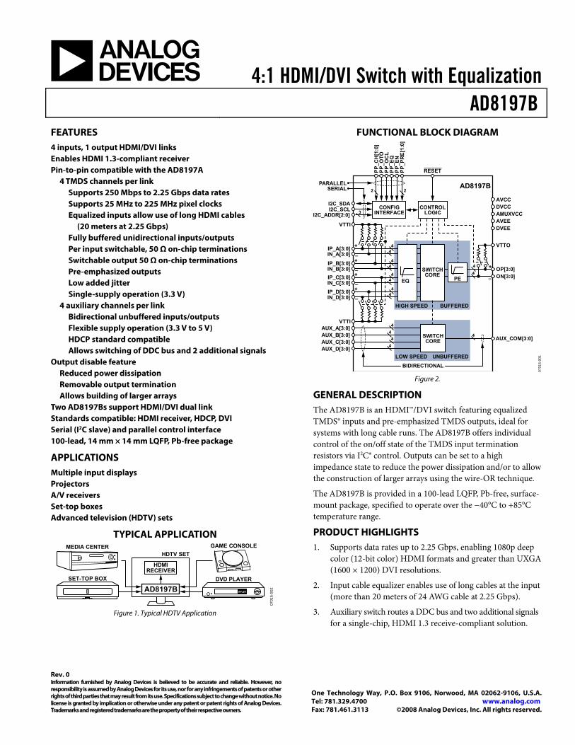
4:1 HDMI/DVI Switch with Equalization AD8197B
Rev. 0 Information furnished by Analog Devices is believed to be accurate and reliable. However, no responsibility is assumed by Analog Devices for its use, nor for any infringements of patents or other rights of third parties that may result from its use. Specifications subject to change without notice. No license is granted by implication or otherwise under any patent or patent rights of Analog Devices. Trademarks and registered trademarks are the property of their respective owners.
One Technology Way, P.O. Box 9106, Norwood, MA 02062-9106, U.S.A.Tel: 781.329.4700 www.analog.com Fax: 781.461.3113 ©2008 Analog Devices, Inc. All rights reserved.
FEATURES 4 inputs, 1 output HDMI/DVI links Enables HDMI 1.3-compliant receiver Pin-to-pin compatible with the AD8197A
4 TMDS channels per link Supports 250 Mbps to 2.25 Gbps data rates Supports 25 MHz to 225 MHz pixel clocks Equalized inputs allow use of long HDMI cables
(20 meters at 2.25 Gbps) Fully buffered unidirectional inputs/outputs Per input switchable, 50 Ω on-chip terminations Switchable output 50 Ω on-chip terminations Pre-emphasized outputs Low added jitter Single-supply operation (3.3 V)
4 auxiliary channels per link Bidirectional unbuffered inputs/outputs Flexible supply operation (3.3 V to 5 V) HDCP standard compatible Allows switching of DDC bus and 2 additional signals
Output disable feature Reduced power dissipation Removable output termination Allows building of larger arrays
Two AD8197Bs support HDMI/DVI dual link Standards compatible: HDMI receiver, HDCP, DVI Serial (I2C slave) and parallel control interface 100-lead, 14 mm × 14 mm LQFP, Pb-free package
APPLICATIONS Multiple input displays Projectors A/V receivers Set-top boxes Advanced television (HDTV) sets
TYPICAL APPLICATION
DVD PLAYER
GAME CONSOLE
SET-TOP BOX
MEDIA CENTERHDTV SET
HDMIRECEIVER
AD8197B 04:20
0701
5-00
2
Figure 1. Typical HDTV Application
FUNCTIONAL BLOCK DIAGRAM
LOW SPEED UNBUFFERED
HIGH SPEED BUFFERED
AVCCDVCCAMUXVCCAVEEDVEE
VTTO
OP[3:0]
AUX_COM[3:0]
ON[3:0]
+
–
4
BIDIRECTIONAL
I2C_SDAI2C_SCL
I2C_ADDR[2:0]
VTTI
VTTI
IP_A[3:0]IN_A[3:0]
+
–IP_B[3:0]IN_B[3:0]
+
–IP_C[3:0]IN_C[3:0]
+
–IP_D[3:0]IN_D[3:0]
AUX_C[3:0]AUX_B[3:0]AUX_A[3:0]
AUX_D[3:0]
+
–
44
44
44
44
444
4
EQ
SWITCHCORE
SWITCHCORE
CONTROLLOGIC
CONFIGINTERFACE3
2 2SERIALPARALLEL
PP_C
H[1
:0]
PP_O
TOPP
_OC
LPP
_EQ
PP_E
NPP
_PR
E[1:
0]
RESET
PE4
4
AD8197B
0701
5-00
1
Figure 2.
GENERAL DESCRIPTION The AD8197B is an HDMI™/DVI switch featuring equalized TMDS® inputs and pre-emphasized TMDS outputs, ideal for systems with long cable runs. The AD8197B offers individual control of the on/off state of the TMDS input termination resistors via I2C® control. Outputs can be set to a high impedance state to reduce the power dissipation and/or to allow the construction of larger arrays using the wire-OR technique.
The AD8197B is provided in a 100-lead LQFP, Pb-free, surface-mount package, specified to operate over the −40°C to +85°C temperature range.
PRODUCT HIGHLIGHTS 1. Supports data rates up to 2.25 Gbps, enabling 1080p deep
color (12-bit color) HDMI formats and greater than UXGA (1600 × 1200) DVI resolutions.
2. Input cable equalizer enables use of long cables at the input (more than 20 meters of 24 AWG cable at 2.25 Gbps).
3. Auxiliary switch routes a DDC bus and two additional signals for a single-chip, HDMI 1.3 receive-compliant solution.
AD8197B
Rev. 0 | Page 2 of 28
TABLE OF CONTENTS Features .............................................................................................. 1 Applications....................................................................................... 1 Typical Application........................................................................... 1 Functional Block Diagram .............................................................. 1 General Description ......................................................................... 1 Product Highlights ........................................................................... 1 Revision History ............................................................................... 2 Specifications..................................................................................... 3 Absolute Maximum Ratings............................................................ 5
Thermal Resistance ...................................................................... 5 Maximum Power Dissipation ..................................................... 5 ESD Caution.................................................................................. 5
Pin Configuration and Function Descriptions............................. 6 Typical Performance Characteristics ............................................. 9 Theory of Operation ...................................................................... 13
Introduction ................................................................................ 13 Input Channels............................................................................ 13 Output Channels ........................................................................ 13 Auxiliary Switch.......................................................................... 14
Serial Control Interface.................................................................. 15 Reset ............................................................................................. 15 Write Procedure.......................................................................... 15 Read Procedure........................................................................... 16
Switching/Update Delay............................................................ 16 Parallel Control Interface .............................................................. 17 Serial Interface Configuration Registers ..................................... 18
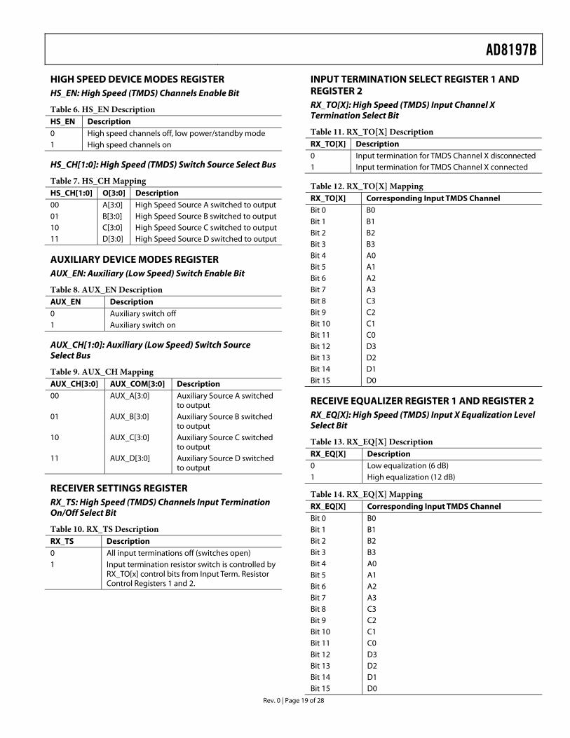
High Speed Device Modes Register......................................... 19 Auxiliary Device Modes Register............................................. 19 Receiver Settings Register ......................................................... 19 Input Termination Select Register 1 and Register 2 .............. 19 Receive Equalizer Register 1 and Register 2 ........................... 19 Transmitter Settings Register.................................................... 20
Parallel Interface Configuration Registers .................................. 21 High Speed Device Modes Register......................................... 22 Auxiliary Device Modes Register............................................. 22 Input Termination Resistor Control Register 1 and Register 2.............................................................................. 22 Receive Equalizer Register 1 and Register 2 ........................... 22 Transmitter Settings Register.................................................... 22
Application Information................................................................ 23 Pinout........................................................................................... 23 Cable Lengths and Equalization............................................... 23 PCB Layout Guidelines.............................................................. 24
Outline Dimensions ....................................................................... 28 Ordering Guide .......................................................................... 28
REVISION HISTORY 1/08—Revision 0: Initial Version
AD8197B
Rev. 0 | Page 3 of 28
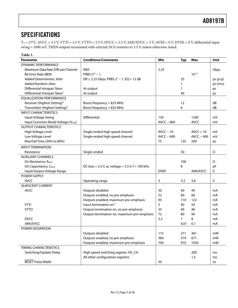
SPECIFICATIONS TA = 27°C, AVCC = 3.3 V, VTTI = 3.3 V, VTTO = 3.3 V, DVCC = 3.3 V, AMUXVCC = 5 V, AVEE = 0 V, DVEE = 0 V, differential input swing = 1000 mV, TMDS outputs terminated with external 50 Ω resistors to 3.3 V, unless otherwise noted.
Table 1. Parameter Conditions/Comments Min Typ Max Unit DYNAMIC PERFORMANCE
Maximum Data Rate (DR) per Channel NRZ 2.25 Gbps Bit Error Rate (BER) PRBS 223 − 1 10−9 Added Deterministic Jitter DR ≤ 2.25 Gbps, PRBS 27 − 1, EQ = 12 dB 25 ps (p-p) Added Random Jitter 1 ps (rms) Differential Intrapair Skew At output 1 ps Differential Interpair Skew1 At output 40 ps
EQUALIZATION PERFORMANCE Receiver (Highest Setting)2 Boost frequency = 825 MHz 12 dB Transmitter (Highest Setting)3 Boost frequency = 825 MHz 6 dB
INPUT CHARACTERISTICS Input Voltage Swing Differential 150 1200 mV Input Common-Mode Voltage (VICM) AVCC − 800 AVCC mV
OUTPUT CHARACTERISTICS High Voltage Level Single-ended high speed channel AVCC − 10 AVCC + 10 mV Low Voltage Level Single-ended high speed channel AVCC − 600 AVCC − 400 mV Rise/Fall Time (20% to 80%) 75 135 200 ps
INPUT TERMINATION Resistance Single-ended 50 Ω
AUXILIARY CHANNELS On Resistance, RAUX 100 Ω On Capacitance, CAUX DC bias = 2.5 V, ac voltage = 3.5 V, f = 100 kHz 8 pF Input/Output Voltage Range DVEE AMUXVCC V
POWER SUPPLY AVCC Operating range 3 3.3 3.6 V
QUIESCENT CURRENT AVCC Outputs disabled 30 40 44 mA
Outputs enabled, no pre-emphasis 52 60 66 mA Outputs enabled, maximum pre-emphasis 95 110 122 mA
VTTI Input termination on4 5 40 54 mA VTTO Output termination on, no pre-emphasis 35 40 46 mA Output termination on, maximum pre-emphasis 72 80 90 mA DVCC 3.2 7 8 mA AMUXVCC 0.01 0.1 mA
POWER DISSIPATION Outputs disabled 115 271 361 mW Outputs enabled, no pre-emphasis 384 574 671 mW Outputs enabled, maximum pre-emphasis 704 910 1050 mW TIMING CHARACTERISTICS
Switching/Update Delay High speed switching register: HS_CH 200 ms All other configuration registers 1.5 ms RESET Pulse Width 50 ns
AD8197B
Rev. 0 | Page 4 of 28
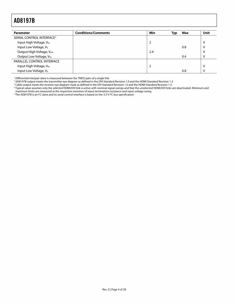
Parameter Conditions/Comments Min Typ Max Unit SERIAL CONTROL INTERFACE5
Input High Voltage, VIH 2 V Input Low Voltage, VIL 0.8 V Output High Voltage, VOH 2.4 V Output Low Voltage, VOL 0.4 V
PARALLEL CONTROL INTERFACE Input High Voltage, VIH 2 V Input Low Voltage, VIL 0.8 V
1 Differential interpair skew is measured between the TMDS pairs of a single link. 2 AD8197B output meets the transmitter eye diagram as defined in the DVI Standard Revision 1.0 and the HDMI Standard Revision 1.3. 3 Cable output meets the receiver eye diagram mask as defined in the DVI Standard Revision 1.0 and the HDMI Standard Revision 1.3. 4 Typical value assumes only the selected HDMI/DVI link is active with nominal signal swings and that the unselected HDMI/DVI links are deactivated. Minimum and
maximum limits are measured at the respective extremes of input termination resistance and input voltage swing. 5 The AD8197B is an I2C slave and its serial control interface is based on the 3.3 V I2C bus specification.
AD8197B
Rev. 0 | Page 5 of 28
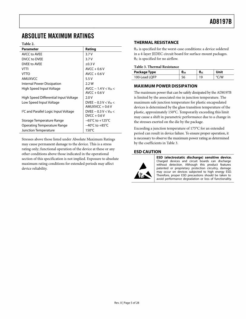
ABSOLUTE MAXIMUM RATINGS Table 2. Parameter Rating AVCC to AVEE 3.7 V DVCC to DVEE 3.7 V DVEE to AVEE ±0.3 V VTTI AVCC + 0.6 V VTTO AVCC + 0.6 V AMUXVCC 5.5 V Internal Power Dissipation 2.2 W High Speed Input Voltage AVCC − 1.4 V < VIN <
AVCC + 0.6 V High Speed Differential Input Voltage 2.0 V Low Speed Input Voltage DVEE − 0.3 V < VIN <
AMUXVCC + 0.6 V I2C and Parallel Logic Input Voltage DVEE − 0.3 V < VIN <
DVCC + 0.6 V Storage Temperature Range −65°C to +125°C Operating Temperature Range −40°C to +85°C Junction Temperature 150°C
Stresses above those listed under Absolute Maximum Ratings may cause permanent damage to the device. This is a stress rating only; functional operation of the device at these or any other conditions above those indicated in the operational section of this specification is not implied. Exposure to absolute maximum rating conditions for extended periods may affect device reliability.
THERMAL RESISTANCE θJA is specified for the worst-case conditions: a device soldered in a 4-layer JEDEC circuit board for surface-mount packages. θJC is specified for no airflow.
Table 3. Thermal Resistance Package Type θJA θJC Unit 100-Lead LQFP 56 19 °C/W
MAXIMUM POWER DISSIPATION The maximum power that can be safely dissipated by the AD8197B is limited by the associated rise in junction temperature. The maximum safe junction temperature for plastic encapsulated devices is determined by the glass transition temperature of the plastic, approximately 150°C. Temporarily exceeding this limit may cause a shift in parametric performance due to a change in the stresses exerted on the die by the package.
Exceeding a junction temperature of 175°C for an extended period can result in device failure. To ensure proper operation, it is necessary to observe the maximum power rating as determined by the coefficients in Table 3.
ESD CAUTION
AD8197B
Rev. 0 | Page 6 of 28
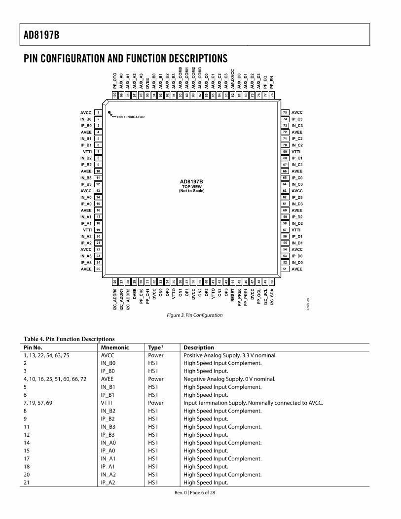
PIN CONFIGURATION AND FUNCTION DESCRIPTIONS
PP_O
TOA
UX_
A0
AU
X_A
1A
UX_
A2
AU
X_A
3D
VEE
AU
X_B
0A
UX_
B1
AU
X_B
2A
UX_
B3
AU
X_C
OM
0A
UX_
CO
M1
AU
X_C
OM
2A
UX_
CO
M3
AU
X_C
0A
UX_
C1
AU
X_C
2A
UX_
C3
AM
UXV
CC
AU
X_D
0A
UX_
D1
AU
X_D
2A
UX_
D3
PP_E
QPP
_EN
26I2
C_A
DD
R0
27I2
C_A
DD
R1
28I2
C_A
DD
R2
29D
VEE
30PP
_CH
031
PP_C
H1
32D
VCC
33O
N0
34O
P035
VTTO
36O
N1
37O
P138
DVC
C39
ON
2
2IN_B03IP_B04AVEE
7VTTI
6IP_B1
5IN_B1
1AVCC
8IN_B29IP_B2
10AVEE
12IP_B313AVCC14IN_A015IP_A016AVEE17IN_A118IP_A119VTTI20IN_A221IP_A222AVCC23IN_A324IP_A325AVEE
11IN_B3
74 IP_C3AVCC
73 IN_C372 AVEE
69 VTTI
70 IN_C2
71 IP_C2
75
68 IP_C167 IN_C166 AVEE
64 IN_C063 AVCC62 IP_D361 IN_D360 AVEE59 IP_D258 IN_D257 VTTI56 IP_D155 IN_D154 AVCC53 IP_D052 IN_D051 AVEE
65 IP_C0
40O
P241
VTTO
42O
N3
43O
P344
RES
ET45
PP_P
RE0
46PP
_PR
E147
DVC
C48
PP_O
CL
49I2
C_S
CL
50I2
C_S
DA
100
99 98 97 96 95 94 93 92 91 90 89 88 87 86 85 84 83 82 81 80 79 78 77 76
PIN 1 INDICATOR
AD8197BTOP VIEW
(Not to Scale)
0701
5-00
3
Figure 3. Pin Configuration
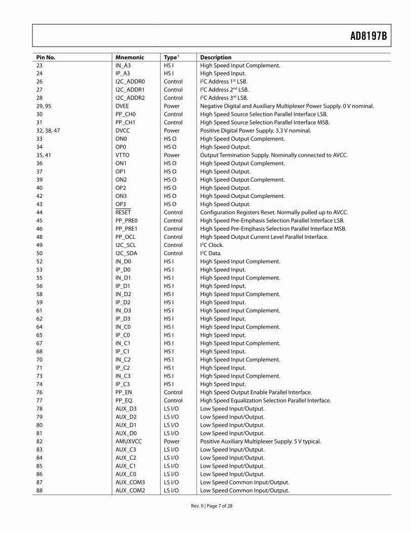
Table 4. Pin Function Descriptions Pin No. Mnemonic Type1 Description 1, 13, 22, 54, 63, 75 AVCC Power Positive Analog Supply. 3.3 V nominal. 2 IN_B0 HS I High Speed Input Complement. 3 IP_B0 HS I High Speed Input. 4, 10, 16, 25, 51, 60, 66, 72 AVEE Power Negative Analog Supply. 0 V nominal. 5 IN_B1 HS I High Speed Input Complement. 6 IP_B1 HS I High Speed Input. 7, 19, 57, 69 VTTI Power Input Termination Supply. Nominally connected to AVCC. 8 IN_B2 HS I High Speed Input Complement. 9 IP_B2 HS I High Speed Input. 11 IN_B3 HS I High Speed Input Complement. 12 IP_B3 HS I High Speed Input. 14 IN_A0 HS I High Speed Input Complement. 15 IP_A0 HS I High Speed Input. 17 IN_A1 HS I High Speed Input Complement. 18 IP_A1 HS I High Speed Input. 20 IN_A2 HS I High Speed Input Complement. 21 IP_A2 HS I High Speed Input.
AD8197B
Rev. 0 | Page 7 of 28
Pin No. Mnemonic Type1 Description 23 IN_A3 HS I High Speed Input Complement. 24 IP_A3 HS I High Speed Input. 26 I2C_ADDR0 Control I2C Address 1st LSB. 27 I2C_ADDR1 Control I2C Address 2nd LSB. 28 I2C_ADDR2 Control I2C Address 3rd LSB. 29, 95 DVEE Power Negative Digital and Auxiliary Multiplexer Power Supply. 0 V nominal. 30 PP_CH0 Control High Speed Source Selection Parallel Interface LSB. 31 PP_CH1 Control High Speed Source Selection Parallel Interface MSB. 32, 38, 47 DVCC Power Positive Digital Power Supply. 3.3 V nominal. 33 ON0 HS O High Speed Output Complement. 34 OP0 HS O High Speed Output. 35, 41 VTTO Power Output Termination Supply. Nominally connected to AVCC. 36 ON1 HS O High Speed Output Complement. 37 OP1 HS O High Speed Output. 39 ON2 HS O High Speed Output Complement. 40 OP2 HS O High Speed Output. 42 ON3 HS O High Speed Output Complement. 43 OP3 HS O High Speed Output. 44 RESET Control Configuration Registers Reset. Normally pulled up to AVCC. 45 PP_PRE0 Control High Speed Pre-Emphasis Selection Parallel Interface LSB. 46 PP_PRE1 Control High Speed Pre-Emphasis Selection Parallel Interface MSB. 48 PP_OCL Control High Speed Output Current Level Parallel Interface. 49 I2C_SCL Control I2C Clock. 50 I2C_SDA Control I2C Data. 52 IN_D0 HS I High Speed Input Complement. 53 IP_D0 HS I High Speed Input. 55 IN_D1 HS I High Speed Input Complement. 56 IP_D1 HS I High Speed Input. 58 IN_D2 HS I High Speed Input Complement. 59 IP_D2 HS I High Speed Input. 61 IN_D3 HS I High Speed Input Complement. 62 IP_D3 HS I High Speed Input. 64 IN_C0 HS I High Speed Input Complement. 65 IP_C0 HS I High Speed Input. 67 IN_C1 HS I High Speed Input Complement. 68 IP_C1 HS I High Speed Input. 70 IN_C2 HS I High Speed Input Complement. 71 IP_C2 HS I High Speed Input. 73 IN_C3 HS I High Speed Input Complement. 74 IP_C3 HS I High Speed Input. 76 PP_EN Control High Speed Output Enable Parallel Interface. 77 PP_EQ Control High Speed Equalization Selection Parallel Interface. 78 AUX_D3 LS I/O Low Speed Input/Output. 79 AUX_D2 LS I/O Low Speed Input/Output. 80 AUX_D1 LS I/O Low Speed Input/Output. 81 AUX_D0 LS I/O Low Speed Input/Output. 82 AMUXVCC Power Positive Auxiliary Multiplexer Supply. 5 V typical. 83 AUX_C3 LS I/O Low Speed Input/Output. 84 AUX_C2 LS I/O Low Speed Input/Output. 85 AUX_C1 LS I/O Low Speed Input/Output. 86 AUX_C0 LS I/O Low Speed Input/Output. 87 AUX_COM3 LS I/O Low Speed Common Input/Output. 88 AUX_COM2 LS I/O Low Speed Common Input/Output.
AD8197B
Rev. 0 | Page 8 of 28
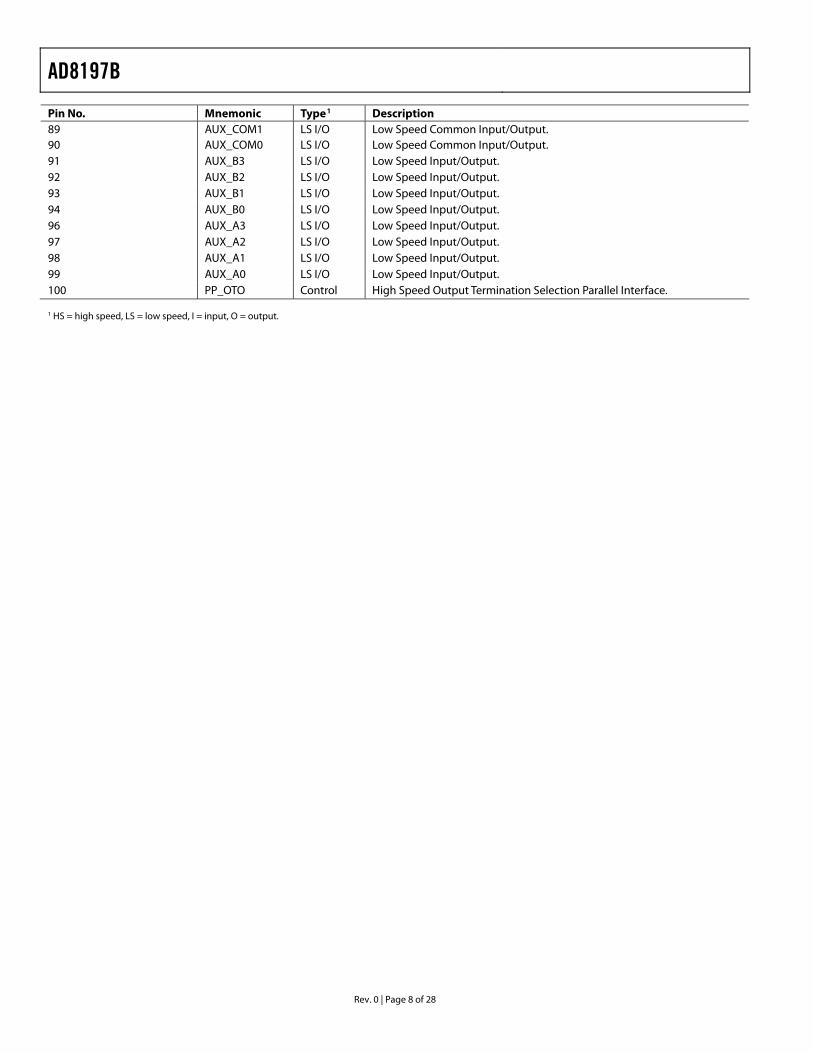
Pin No. Mnemonic Type1 Description 89 AUX_COM1 LS I/O Low Speed Common Input/Output. 90 AUX_COM0 LS I/O Low Speed Common Input/Output. 91 AUX_B3 LS I/O Low Speed Input/Output. 92 AUX_B2 LS I/O Low Speed Input/Output. 93 AUX_B1 LS I/O Low Speed Input/Output. 94 AUX_B0 LS I/O Low Speed Input/Output. 96 AUX_A3 LS I/O Low Speed Input/Output. 97 AUX_A2 LS I/O Low Speed Input/Output. 98 AUX_A1 LS I/O Low Speed Input/Output. 99 AUX_A0 LS I/O Low Speed Input/Output. 100 PP_OTO Control High Speed Output Termination Selection Parallel Interface. 1 HS = high speed, LS = low speed, I = input, O = output.
AD8197B
Rev. 0 | Page 9 of 28
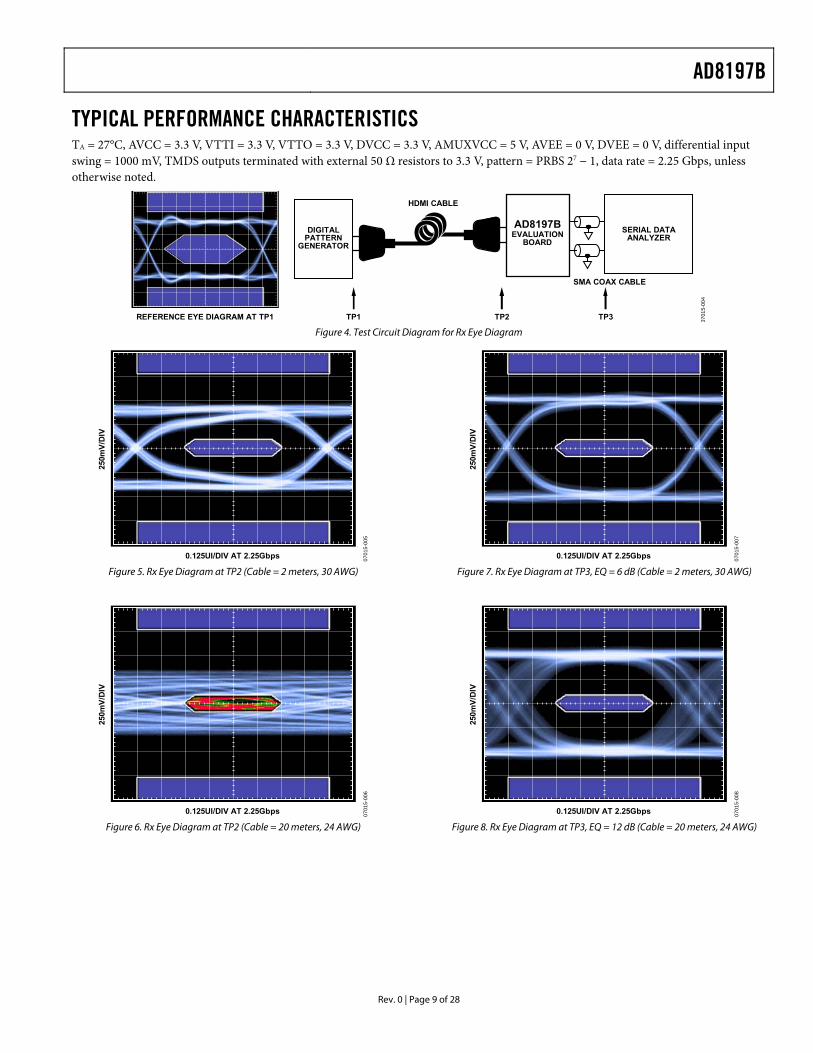
TYPICAL PERFORMANCE CHARACTERISTICS TA = 27°C, AVCC = 3.3 V, VTTI = 3.3 V, VTTO = 3.3 V, DVCC = 3.3 V, AMUXVCC = 5 V, AVEE = 0 V, DVEE = 0 V, differential input swing = 1000 mV, TMDS outputs terminated with external 50 Ω resistors to 3.3 V, pattern = PRBS 27 − 1, data rate = 2.25 Gbps, unless otherwise noted.
REFERENCE EYE DIAGRAM AT TP1
DIGITALPATTERN
GENERATOR
AD8197BEVALUATION
BOARDSERIAL DATA
ANALYZER
SMA COAX CABLE
HDMI CABLE
TP1 TP2 TP3 0701
5-00
4
Figure 4. Test Circuit Diagram for Rx Eye Diagram
0.125UI/DIV AT 2.25Gbps
250m
V/D
IV
0701
5-00
5
Figure 5. Rx Eye Diagram at TP2 (Cable = 2 meters, 30 AWG)
0.125UI/DIV AT 2.25Gbps
250m
V/D
IV
0701
5-00
6
Figure 6. Rx Eye Diagram at TP2 (Cable = 20 meters, 24 AWG)
0.125UI/DIV AT 2.25Gbps
250m
V/D
IV
0701
5-00
7
Figure 7. Rx Eye Diagram at TP3, EQ = 6 dB (Cable = 2 meters, 30 AWG)
0.125UI/DIV AT 2.25Gbps
250m
V/D
IV
0701
5-00
8
Figure 8. Rx Eye Diagram at TP3, EQ = 12 dB (Cable = 20 meters, 24 AWG)
AD8197B
Rev. 0 | Page 10 of 28
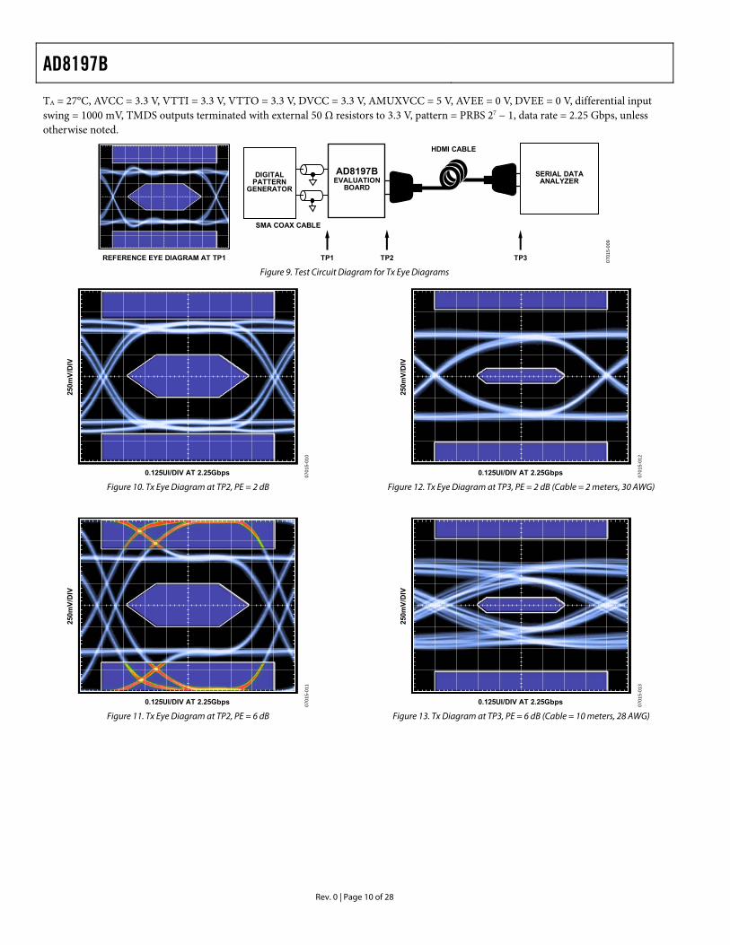
TA = 27°C, AVCC = 3.3 V, VTTI = 3.3 V, VTTO = 3.3 V, DVCC = 3.3 V, AMUXVCC = 5 V, AVEE = 0 V, DVEE = 0 V, differential input swing = 1000 mV, TMDS outputs terminated with external 50 Ω resistors to 3.3 V, pattern = PRBS 27 − 1, data rate = 2.25 Gbps, unless otherwise noted.
REFERENCE EYE DIAGRAM AT TP1
DIGITALPATTERN
GENERATOR
SMA COAX CABLE
HDMI CABLE
TP1 TP2 TP3
AD8197BEVALUATION
BOARD
SERIAL DATAANALYZER
0701
5-00
9
Figure 9. Test Circuit Diagram for Tx Eye Diagrams
0.125UI/DIV AT 2.25Gbps
250m
V/D
IV
0701
5-01
0
Figure 10. Tx Eye Diagram at TP2, PE = 2 dB
0.125UI/DIV AT 2.25Gbps
250m
V/D
IV
0701
5-01
1
Figure 11. Tx Eye Diagram at TP2, PE = 6 dB
0.125UI/DIV AT 2.25Gbps
250m
V/D
IV
0701
5-01
2
Figure 12. Tx Eye Diagram at TP3, PE = 2 dB (Cable = 2 meters, 30 AWG)
0.125UI/DIV AT 2.25Gbps
250m
V/D
IV
0701
5-01
3
Figure 13. Tx Diagram at TP3, PE = 6 dB (Cable = 10 meters, 28 AWG)
AD8197B
Rev. 0 | Page 11 of 28
TA = 27°C, AVCC = 3.3 V, VTTI = 3.3 V, VTTO = 3.3 V, DVCC = 3.3 V, AMUXVCC = 5 V, AVEE = 0 V, DVEE = 0 V, differential input swing = 1000 mV, TMDS outputs terminated with external 50 Ω resistors to 3.3 V, pattern = PRBS 27 − 1, data rate = 2.25 Gbps, unless otherwise noted.
0.5
0.6
00 25
HDMI CABLE LENGTH (m)
DET
ERM
INIS
TIC
JIT
TER
(UI)
0.4
0.3
0.2
0.1
5 10 15 20
2m CABLE = 30AWG5m TO 20m CABLES = 24AWG
1.65GbpsEQ = 12dB
2.25GbpsEQ = 12dB
2.25GbpsEQ = 6dB
1.65GbpsEQ = 6dB
0701
5-01
4
DATA RATE (Gbps)
JITT
ER (p
s)
Figure 14. Jitter vs. Input Cable Length (See Figure 4 for Test Setup)
50
00 2.4
45
40
35
30
25
20
15
10
5
0.2 0.4 0.6 0.8 1.0 1.2 1.4 1.6 1.8 2.0 2.2
1080p12-BIT
1.65Gbps
1080p8-BIT
1080i/720p
480i
480p
DJ (p-p)
RJ (rms)
0701
5-01
5
Figure 15. Jitter vs. Data Rate
50
03.0 3.6
SUPPLY VOLTAGE (V)
JITT
ER (p
s)
45
40
35
30
25
20
15
10
5
3.1 3.2 3.3 3.4 3.5
RJ (rms)
DJ (p-p)
0701
5-01
6
Figure 16. Jitter vs. Supply Voltage
0.5
0.6
00 20
HDMI CABLE LENGTH (m)
DET
ERM
INIS
TIC
JIT
TER
(UI)
0.4
0.3
0.2
0.1
2m CABLE = 30AWG5m TO 20m CABLES = 24AWG
5 10 15
1.65Gbps, PE MAX
2.25Gbps, PE MAX
1.65Gbps, PE OFF
2.25Gbps, PE OFF
0701
5-01
7
1200
00
DATA RATE (Gbps)
EYE
HEI
GH
T (m
V)
Figure 17. Jitter vs. Output Cable Length (See Figure 9 for Test Setup)
1000
800
600
400
200
2.4
0701
5-01
80.2 0.4 0.6 0.8 1.0 1.2 1.4 1.6 1.8 2.0 2.2
Figure 18. Eye Height vs. Data Rate
800
02.5 3.6
SUPPLY VOLTAGE (V)
EYE
HEI
GH
T (m
V)
700
600
500
400
300
200
100
2.6 2.7 2.8 2.9 3.0 3.1 3.2 3.3 3.4 3.5
0701
5-01
9
Figure 19. Eye Height vs. Supply Voltage
AD8197B
Rev. 0 | Page 12 of 28
DIFFERENTIAL INPUT SWING (V)
JITT
ER (p
s)
TA = 27°C, AVCC = 3.3 V, VTTI = 3.3 V, VTTO = 3.3 V, DVCC = 3.3 V, AMUXVCC = 5 V, AVEE = 0 V, DVEE = 0 V, differential input swing = 1000 mV, TMDS outputs terminated with external 50 Ω resistors to 3.3 V, pattern = PRBS 27 − 1, data rate = 2.25 Gbps, unless otherwise noted.
00 2
40
50
30
20
10
.0
50
02.5 3.7
INPUT COMMON-MODE VOLTAGE (V)
JITT
ER (p
s)
0.2 0.4 0.6 0.8 1.0 1.2 1.4 1.6 1.8
RJ (rms)
DJ (p-p)
0701
5-02
0
Figure 20. Jitter vs. Differential Input Swing
50
0–40 100
TEMPERATURE (°C)
JITT
ER (p
s)
45
40
35
30
25
20
15
10
5
–20 0 20 40 60 80
DJ (p-p)
RJ (rms)
0701
5-02
1
Figure 21. Jitter vs. Temperature
160
0–40 100
TEMPERATURE (°C)
RIS
E/FA
LL T
IME
20%
TO
80%
(ps)
140
120
100
80
60
40
20
–20 0 20 40 60 80
RISE TIME
FALL TIME
0701
5-02
2
Figure 22. Rise and Fall Time vs. Temperature
40
30
20
10
DJ (p-p)
RJ (rms)
0701
5-02
32.7 2.9 3.1 3.3 3.5
Figure 23. Jitter vs. Input Common-Mode Voltage
120
80–40 100
TEMPERATURE (°C)
DIF
FER
ENTI
AL
INPU
TTE
RM
INA
TIO
N R
ESIS
TAN
CE
(Ω)
115
110
105
100
95
90
85
–20 0 20 40 60 80
0701
5-02
4
Figure 24. Differential Input Termination Resistance vs. Temperature
AD8197B
Rev. 0 | Page 13 of 28
THEORY OF OPERATION INTRODUCTION The AD8197B is a pin-to-pin HDMI 1.3 receive-compliant replacement for the AD8197A. The primary function of the AD8197B is to switch one of four (HDMI or DVI) single link sources to one output. Each HDMI/DVI link consists of four differential, high speed channels and four auxiliary single-ended, low speed control signals. The high speed channels include a data-word clock and three transition minimized differ-ential signaling (TMDS) data channels running at 10× the data-word clock frequency for data rates up to 2.25 Gbps. The four low speed control signals are 5 V tolerant bidirectional lines that can carry configuration signals, HDCP encryption, and other information, depending upon the specific application.
All four high speed TMDS channels in a given link are identical; that is, the pixel clock can be run on any of the four TMDS channels. Transmit and receive channel compensation is provided for the high speed channels where the user can (manually) select among a number of fixed settings.
The AD8197B has two control interfaces. Users have the option of controlling the part through either the parallel control interface or the I2C serial control interface. However, the parallel control interface is not able to control the switch status of the input termination resistors and therefore has limited usefulness in practical systems. Most systems use only the I2C serial interface.
The AD8197B has eight user-programmable I2C slave addresses to allow multiple AD8197Bs to be controlled by a single I2C bus. A RESET pin is provided to restore the control registers of the AD8197B to the parallel control interface and some default values. In all cases, serial programming values override any prior parallel programming values, and any use of the serial control interface disables the parallel control interface until the AD8197B is reset.
INPUT CHANNELS Each high speed input differential pair terminates to the 3.3 V VTTI power supply through a pair of single-ended 50 Ω on-chip resistors, as shown in Figure 25. The input termination status for each individual high speed differential (TMDS) input pair can be controlled by programming the appropriate RX_TO bit in the receiver settings register. Refer to Table 5 and Table 12. By default, the input terminations are disabled (switched open) after reset. The input terminations cannot be switched when programming the AD8197B through the parallel control interface. This limits the usefulness of the parallel control interface.
Some systems require that the input terminations be switched on only for the one selected HDMI source. The input termina-tions for the three unselected HDMI sources require their input termination switches to be open. The AD8197B can perform
this operation, but it is not automatic. To obtain this functionality, the channel selection and the input termination status must be separately programmed via the I2C serial control interface.
CABLEEQ
50Ω50Ω
IP_xxIN_xx
AVEE
VTTI
0701
5-03
5
Figure 25. High Speed Input Simplified Schematic
The input equalizer can be manually configured to provide two different levels of high frequency boost: 6 dB or 12 dB. The user can individually control the equalization level of the eight high speed input channels by selectively programming the associated RX_EQ bits in the receive equalizer register through the serial control interface. Alternately, the user can globally control the equalization level of all eight high speed input channels by setting the PP_EQ pin of the parallel control interface. No specific cable length is suggested for a particular equalization setting because cable performance varies widely between manufacturers; however, in general, the equalization of the AD8197B can be set to 12 dB without degrading the signal integrity, even for short input cables. At the 12 dB setting, the AD8197B can equalize more than 20 meters of 24 AWG cable at 2.25 Gbps.
OUTPUT CHANNELS Each high speed output differential pair is terminated to the 3.3 V VTTO power supply through two 50 Ω on-chip resistors (see Figure 26). This termination is user-selectable; it can be turned on or off by programming the TX_PTO bit of the transmitter settings register through the serial control interface, or by setting the PP_OTO pin of the parallel control interface.
The output termination resistors of the AD8197B back-terminate the output TMDS transmission lines. These back-terminations, as recommended in the HDMI 1.3 specification, act to absorb reflections from impedance discontinuities on the output traces, improving the signal integrity of the output traces and adding flexibility to how the output traces can be routed. For example, interlayer vias can be used to route the AD8197B TMDS outputs on multiple layers of the PCB without severely degrading the quality of the output signal.
The AD8197B output has a disable feature that places the outputs in a tristate mode. This mode is enabled by program-ming the HS_EN bit of the high speed device modes register through the serial control interface or by setting the PP_EN pin of the parallel control interface. Larger wire-OR’ed arrays can be constructed using the AD8197B in this mode.
AD8197B
Rev. 0 | Page 14 of 28
VTTO
50Ω50Ω
OPx ONx
AVEE
DISABLE IOUT
0701
5-02
5
Figure 26. High Speed Output Simplified Schematic
The AD8197B requires output termination resistors when the high speed outputs are enabled. Termination can be internal and/or external. The internal terminations of the AD8197B are enabled by programming the TX_PTO bit of the transmitter settings register or by setting the PP_OTO pin of the parallel control interface. The internal terminations of the AD8197B default to the setting indicated by PP_OTO upon reset. External terminations can be provided either by on-board resistors or by the input termination resistors of an HDMI/DVI receiver. If both the internal terminations are enabled and external termi-nations are present, set the output current level to 20 mA by programming the TX_OCL bit of the transmitter settings register through the serial control interface or by setting the PP_OCL pin of the parallel control interface. The output current level defaults to the level indicated by PP_OCL upon reset. If only external terminations are provided (if the internal terminations are disabled), set the output current level to 10 mA by programming the TX_OCL bit of the transmitter settings register or by setting the PP_OCL pin of the parallel control interface. The high speed outputs must be disabled if there are no output termination resistors present in the system.
The output pre-emphasis can be manually configured to provide one of four different levels of high frequency boost. The specific boost level is selected by programming the TX_PE bits of the transmitter settings register through the serial control interface, or by setting the PP_PE bus of the parallel control interface. No specific cable length is suggested for a particular pre-emphasis setting because cable performance varies widely between manufacturers.
AUXILIARY SWITCH The auxiliary (low speed) lines have no amplification. They are routed using a passive switch that is bandwidth compatible with standard speed I2C. The schematic equivalent for this passive connection is shown in Figure 27.
AUX_COM0AUX_A0
½CAUX ½CAUX
RAUX
0701
5-02
6
Figure 27. Auxiliary Channel Simplified Schematic,
AUX_A0 to AUX_COM0 Routing Example
When turning off the AD8197B, care needs to be taken with the AMUXVCC supply to ensure that the auxiliary multiplexer pins remain in a high impedance state. A scenario that illustrates this requirement is one where the auxiliary multiplexer is used to switch the display data channel (DDC) bus. In some applica-tions, additional devices can be connected to the DDC bus (such as an EEPROM with EDID information) upstream of the AD8197B.
Extended display identification data (EDID) is a VESA standard-defined data format for conveying display configuration information to sources to optimize display use. EDID devices may need to be available via the DDC bus, regardless of the state of the AD8197B and any downstream circuit. For this configuration, the auxiliary inputs of the powered down AD8197B need to be in a high impedance state to avoid pulling down on the DDC lines and preventing these other devices from using the bus.
The AD8197B requires +5 V on its supply pin, AMUXVCC, in order for the AUXMUX channels to be high impedance. When a TV is powered off, it cannot provide such a supply. However, it can be provided from any HDMI source that is plugged into it. A Schottky diode network, as shown in Figure 28, uses the 5 V supply (Pin 18) from any HDMI/DVI source to power AMUXVCC and guarantee high impedance of the auxiliary multiplexer pins. The AMUXVCC supply does not draw any significant static current. The use of diodes ensures that connected HDMI sources do not load this circuit if their +5 V pin is low impedance when powered off. The 100 kΩ resistor ensures that a minimum of current flows through the diodes to keep them forward biased.
This precaution does not need to be taken if the DDC peripheral circuitry is connected to the bus downstream of the AD8197B.
PERIPHERALCIRCUITRY
PERIPHERALCIRCUITRY
+5V SOURCE C
+5V SOURCE D
PIN 18 HDMI CONNECTORPIN 14 DVI CONNECTOR
PIN 18 HDMI CONNECTORPIN 14 DVI CONNECTOR
I<50mA
I<50mA
PERIPHERALCIRCUITRY
PERIPHERALCIRCUITRY
SOURCE A +5V
SOURCE B +5V
PIN 18 HDMI CONNECTORPIN 14 DVI CONNECTOR
PIN 18 HDMI CONNECTORPIN 14 DVI CONNECTOR
I<50mA
I<50mA
AMUXVCC
AD8197B
+5V INTERNAL(IF ANY)
0701
5-02
7
BAT54L BAT54LBAT54L
BAT54L BAT54L
100kΩ
Figure 28. Suggested AMUXVCC Power Scheme
AD8197B
Rev. 0 | Page 15 of 28
SERIAL CONTROL INTERFACE RESET On initial power-up, or at any point in operation, the AD8197B register set can be restored to the status of the parallel control interface pins and some preprogrammed default values by pulling the RESET pin to low, in accordance with the specifica-tions in Table 1. During normal operation, however, the RESET pin must be pulled up to 3.3 V. Following a reset, the prepro-grammed default values of the AD8197B register set correspond to the state of the parallel interface configuration registers and defaults, as listed in Table 18. The AD8197B can be controlled through the parallel control interface until the first serial control event occurs. As soon as any serial control event occurs, the serial programming values, corresponding to the state of the serial interface configuration registers (Table 5), override any prior parallel programming values, and the parallel control interface is disabled until the part is subsequently reset.
Note that the input termination resistor switch control is only via I2C control. Therefore, any system that requires control of these switches cannot operate in parallel control mode.
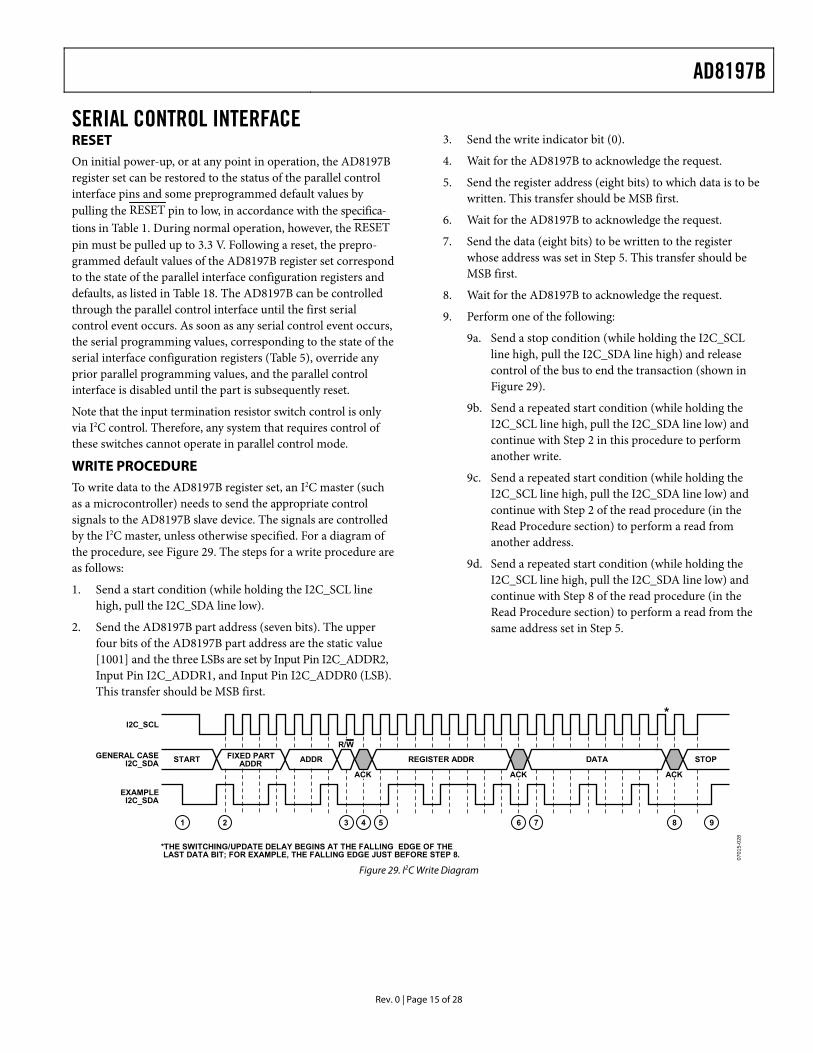
WRITE PROCEDURE To write data to the AD8197B register set, an I2C master (such as a microcontroller) needs to send the appropriate control signals to the AD8197B slave device. The signals are controlled by the I2C master, unless otherwise specified. For a diagram of the procedure, see Figure 29. The steps for a write procedure are as follows:
1. Send a start condition (while holding the I2C_SCL line high, pull the I2C_SDA line low).
2. Send the AD8197B part address (seven bits). The upper four bits of the AD8197B part address are the static value [1001] and the three LSBs are set by Input Pin I2C_ADDR2, Input Pin I2C_ADDR1, and Input Pin I2C_ADDR0 (LSB). This transfer should be MSB first.
3. Send the write indicator bit (0).
4. Wait for the AD8197B to acknowledge the request.
5. Send the register address (eight bits) to which data is to be written. This transfer should be MSB first.
6. Wait for the AD8197B to acknowledge the request.
7. Send the data (eight bits) to be written to the register whose address was set in Step 5. This transfer should be MSB first.
8. Wait for the AD8197B to acknowledge the request.
9. Perform one of the following:
9a. Send a stop condition (while holding the I2C_SCL line high, pull the I2C_SDA line high) and release control of the bus to end the transaction (shown in Figure 29).
9b. Send a repeated start condition (while holding the I2C_SCL line high, pull the I2C_SDA line low) and continue with Step 2 in this procedure to perform another write.
9c. Send a repeated start condition (while holding the I2C_SCL line high, pull the I2C_SDA line low) and continue with Step 2 of the read procedure (in the Read Procedure section) to perform a read from another address.
9d. Send a repeated start condition (while holding the I2C_SCL line high, pull the I2C_SDA line low) and continue with Step 8 of the read procedure (in the Read Procedure section) to perform a read from the same address set in Step 5.
R/W
ACK ACK
ADDRSTART FIXED PARTADDR REGISTER ADDR DATA STOP
ACK
1 2 3 4 5 6 7 8 9
I2C_SCL
GENERAL CASEI2C_SDA
EXAMPLEI2C_SDA
*THE SWITCHING/UPDATE DELAY BEGINS AT THE FALLING EDGE OF THE LAST DATA BIT; FOR EXAMPLE, THE FALLING EDGE JUST BEFORE STEP 8.
*
0701
5-02
8
Figure 29. I2C Write Diagram
AD8197B
Rev. 0 | Page 16 of 28
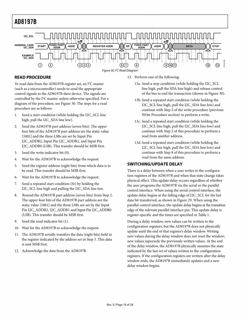
START FIXED PARTADDR REGISTER ADDR FIXED PART
ADDR DATA STOP
ACK
ADDR
ACK
R/W
ADDR
ACK ACK
R/W
SR
1 2 3 4 5 6 7 8 9 10 11 12 13
I2C_SCL
GENERAL CASEI2C_SDA
EXAMPLEI2C_SDA
0701
5-02
9
Figure 30. I2C Read Diagram
READ PROCEDURE To read data from the AD8197B register set, an I2C master (such as a microcontroller) needs to send the appropriate control signals to the AD8197B slave device. The signals are controlled by the I2C master, unless otherwise specified. For a diagram of the procedure, see Figure 30. The steps for a read procedure are as follows:
1. Send a start condition (while holding the I2C_SCL line high, pull the I2C_SDA line low).
2. Send the AD8197B part address (seven bits). The upper four bits of the AD8197B part address are the static value [1001] and the three LSBs are set by Input Pin I2C_ADDR2, Input Pin I2C_ADDR1, and Input Pin I2C_ADDR0 (LSB). This transfer should be MSB first.
3. Send the write indicator bit (0).
4. Wait for the AD8197B to acknowledge the request.
5. Send the register address (eight bits) from which data is to be read. This transfer should be MSB first.
6. Wait for the AD8197B to acknowledge the request.
7. Send a repeated start condition (Sr) by holding the I2C_SCL line high and pulling the I2C_SDA line low.
8. Resend the AD8197B part address (seven bits) from Step 2. The upper four bits of the AD8197B part address are the static value [1001] and the three LSBs are set by the Input Pin I2C_ADDR2, I2C_ADDR1 and Input Pin I2C_ADDR0 (LSB). This transfer should be MSB first.
9. Send the read indicator bit (1).
10. Wait for the AD8197B to acknowledge the request.
11. The AD8197B serially transfers the data (eight bits) held in the register indicated by the address set in Step 5. This data is sent MSB first.
12. Acknowledge the data from the AD8197B.
13. Perform one of the following:
13a. S op condition (while holding the I2C_SCL line high, pull the SDA line high) and release control of the bus to end the transaction (shown in
end a st
).
13b. ted start condition (while holding the
13c.
13d. on (while holding the
SWITCH writes to the configura-
s
tion
lly
w;
y
Figure 30
Send a repeaI2C_SCL line high, pull the I2C_SDA line low) and continue with Step 2 of the write procedure (previous Write Procedure section) to perform a write.
Send a repeated start condition (while holding the I2C_SCL line high, pull the I2C_SDA line low) andcontinue with Step 2 of this procedure to perform a read from another address.
Send a repeated start conditiI2C_SCL line high, pull the I2C_SDA line low) and continue with Step 8 of this procedure to perform a read from the same address.
ING/UPDATE DELAY There is a delay between when a usertion registers of the AD8197B and when that state change takephysical effect. This update delay occurs regardless of whether the user programs the AD8197B via the serial or the parallel control interface. When using the serial control interface, the update delay begins at the falling edge of I2C_SCL for the last data bit transferred, as shown in Figure 29. When using the parallel control interface, the update delay begins at the transiedge of the relevant parallel interface pin. This update delay is register-specific and the times are specified in Table 1.
During a delay window, new values can be written to the configuration registers, but the AD8197B does not physicaupdate until the end of that register’s delay window. Writing new values during the delay window does not reset the windonew values supersede the previously written values. At the end of the delay window, the AD8197B physically assumes the state indicated by the last set of values written to the configuration registers. If the configuration registers are written after the delawindow ends, the AD8197B immediately updates and a new delay window begins.
AD8197B
Rev. 0 | Page 17 of 28
PARALLEL CONTROL INTERFACE The AD8197B can be partially controlled through the parallel interface using the PP_EN, PP_CH[1:0], PP_EQ, PP_PRE[1:0], PP_OTO, and PP_OCL pins. Logic levels for the parallel interface pins are set in accordance with the specifications listed in Table 1. Setting these pins updates the parallel control interface registers, as listed in Table 18. Following a reset, the AD8197B can be controlled through the parallel control interface until the first serial control event occurs. As soon as any serial control event occurs, the serial programming values override any prior parallel programming values, and the parallel control interface is disabled until the part is subsequently reset. The default serial programming values correspond to the state of the serial interface configuration registers, as listed in Table 5.
Note that after changing the status of the channel selection (PP_CH[1:0]), it is necessary to assert a low logic level to RESET to ensure that the channel select status is properly updated.
Note also that the input termination resistor switches can be controlled only via serial programming. Therefore, as most systems require controlling these resistors, serial control is required and parallel control is of little use. However, the parallel control pins determine the AD8197B status between the time of the assertion of reset and the first serial program-ming event.
AD8197B
Rev. 0 | Page 18 of 28
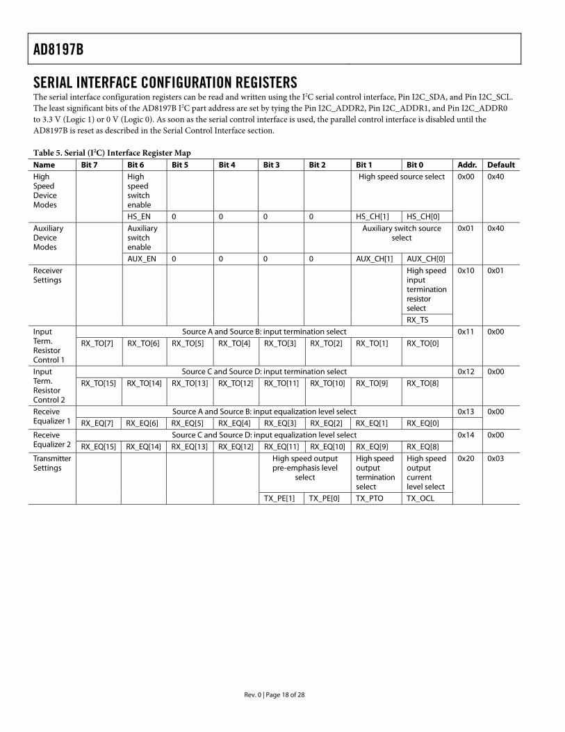
SERIAL INTERFACE CONFIGURATION REGISTERS The serial interface configuration registers can be read and written using the I2C serial control interface, Pin I2C_SDA, and Pin I2C_SCL. The least significant bits of the AD8197B I2C part address are set by tying the Pin I2C_ADDR2, Pin I2C_ADDR1, and Pin I2C_ADDR0 to 3.3 V (Logic 1) or 0 V (Logic 0). As soon as the serial control interface is used, the parallel control interface is disabled until the AD8197B is reset as described in the Serial Control Interface section.
Table 5. Serial (I2C) Interface Register Map Name Bit 7 Bit 6 Bit 5 Bit 4 Bit 3 Bit 2 Bit 1 Bit 0 Addr. Default
High speed switch enable
High speed source select High Speed Device Modes
HS_EN 0 0 0 0 HS_CH[1] HS_CH[0]
0x00 0x40
Auxiliary switch enable
Auxiliary switch source select
Auxiliary Device Modes
AUX_EN 0 0 0 0 AUX_CH[1] AUX_CH[0]
0x01 0x40
High speed input termination resistor select
Receiver Settings
RX_TS
0x10 0x01
Source A and Source B: input termination select Input Term. Resistor Control 1
RX_TO[7] RX_TO[6] RX_TO[5] RX_TO[4] RX_TO[3] RX_TO[2] RX_TO[1] RX_TO[0] 0x11 0x00
Source C and Source D: input termination select 0x12 0x00 Input Term. Resistor Control 2
RX_TO[15] RX_TO[14] RX_TO[13] RX_TO[12] RX_TO[11] RX_TO[10] RX_TO[9] RX_TO[8]
Source A and Source B: input equalization level select 0x13 0x00 Receive Equalizer 1 RX_EQ[7] RX_EQ[6] RX_EQ[5] RX_EQ[4] RX_EQ[3] RX_EQ[2] RX_EQ[1] RX_EQ[0]
Source C and Source D: input equalization level select Receive Equalizer 2 RX_EQ[15] RX_EQ[14] RX_EQ[13] RX_EQ[12] RX_EQ[11] RX_EQ[10] RX_EQ[9] RX_EQ[8]
0x14 0x00
High speed output pre-emphasis level
select
High speed output termination select
High speed output current level select
Transmitter Settings
TX_PE[1] TX_PE[0] TX_PTO TX_OCL
0x20 0x03
AD8197B
Rev. 0 | Page 19 of 28
HIGH SPEED DEVICE MODES REGISTER HS_EN: High Speed (TMDS) Channels Enable Bit
Table 6. HS_EN Description HS_EN Description 0 High speed channels off, low power/standby mode 1 High speed channels on
HS_CH[1:0]: High Speed (TMDS) Switch Source Select Bus
Table 7. HS_CH Mapping HS_CH[1:0] O[3:0] Description 00 A[3:0] High Speed Source A switched to output 01 B[3:0] High Speed Source B switched to output 10 C[3:0] High Speed Source C switched to output 11 D[3:0] High Speed Source D switched to output
AUXILIARY DEVICE MODES REGISTER AUX_EN: Auxiliary (Low Speed) Switch Enable Bit
Table 8. AUX_EN Description AUX_EN Description 0 Auxiliary switch off 1 Auxiliary switch on
AUX_CH[1:0]: Auxiliary (Low Speed) Switch Source Select Bus
Table 9. AUX_CH Mapping AUX_CH[3:0] AUX_COM[3:0] Description 00 AUX_A[3:0] Auxiliary Source A switched
to output 01 AUX_B[3:0] Auxiliary Source B switched
to output 10 AUX_C[3:0] Auxiliary Source C switched
to output 11 AUX_D[3:0] Auxiliary Source D switched
to output
RECEIVER SETTINGS REGISTER RX_TS: High Speed (TMDS) Channels Input Termination On/Off Select Bit
Table 10. RX_TS Description RX_TS Description 0 All input terminations off (switches open) 1 Input termination resistor switch is controlled by
RX_TO[x] control bits from Input Term. Resistor Control Registers 1 and 2.
INPUT TERMINATION SELECT REGISTER 1 AND REGISTER 2 RX_TO[X]: High Speed (TMDS) Input Channel X Termination Select Bit
Table 11. RX_TO[X] Description RX_TO[X] Description 0 Input termination for TMDS Channel X disconnected 1 Input termination for TMDS Channel X connected
Table 12. RX_TO[X] Mapping RX_TO[X] Corresponding Input TMDS Channel Bit 0 B0 Bit 1 B1 Bit 2 B2 Bit 3 B3 Bit 4 A0 Bit 5 A1 Bit 6 A2 Bit 7 A3 Bit 8 C3 Bit 9 C2 Bit 10 C1 Bit 11 C0 Bit 12 D3 Bit 13 D2 Bit 14 D1 Bit 15 D0
RECEIVE EQUALIZER REGISTER 1 AND REGISTER 2 RX_EQ[X]: High Speed (TMDS) Input X Equalization Level Select Bit
Table 13. RX_EQ[X] Description RX_EQ[X] Description 0 Low equalization (6 dB) 1 High equalization (12 dB)
Table 14. RX_EQ[X] Mapping RX_EQ[X] Corresponding Input TMDS Channel Bit 0 B0 Bit 1 B1 Bit 2 B2 Bit 3 B3 Bit 4 A0 Bit 5 A1 Bit 6 A2 Bit 7 A3 Bit 8 C3 Bit 9 C2 Bit 10 C1 Bit 11 C0 Bit 12 D3 Bit 13 D2 Bit 14 D1 Bit 15 D0
AD8197B
Rev. 0 | Page 20 of 28
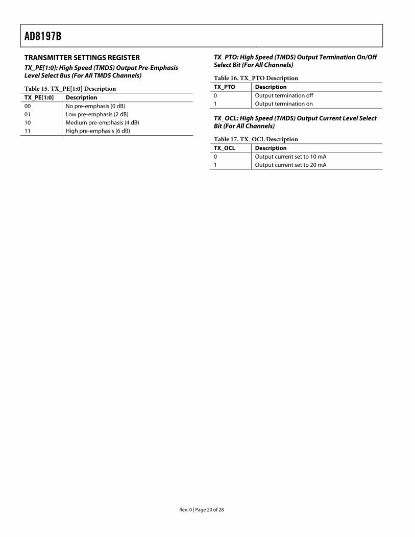
TRANSMITTER SETTINGS REGISTER TX_PE[1:0]: High Speed (TMDS) Output Pre-Emphasis Level Select Bus (For All TMDS Channels)
Table 15. TX_PE[1:0] Description TX_PE[1:0] Description 00 No pre-emphasis (0 dB) 01 Low pre-emphasis (2 dB) 10 Medium pre-emphasis (4 dB) 11 High pre-emphasis (6 dB)
TX_PTO: High Speed (TMDS) Output Termination On/Off Select Bit (For All Channels)
Table 16. TX_PTO Description TX_PTO Description 0 Output termination off 1 Output termination on
TX_OCL: High Speed (TMDS) Output Current Level Select Bit (For All Channels)
Table 17. TX_OCL Description TX_OCL Description 0 Output current set to 10 mA 1 Output current set to 20 mA
AD8197B
Rev. 0 | Page 21 of 28
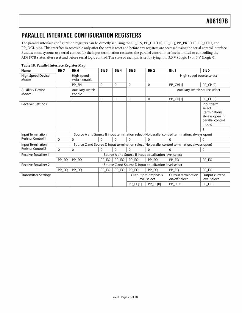
PARALLEL INTERFACE CONFIGURATION REGISTERS The parallel interface configuration registers can be directly set using the PP_EN, PP_CH[1:0], PP_EQ, PP_PRE[1:0], PP_OTO, and PP_OCL pins. This interface is accessible only after the part is reset and before any registers are accessed using the serial control interface. Because most systems use serial control for the input termination resistors, the parallel control interface is limited to controlling the AD8197B status after reset and before serial logic control. The state of each pin is set by tying it to 3.3 V (Logic 1) or 0 V (Logic 0).
Table 18. Parallel Interface Register Map Name Bit 7 Bit 6 Bit 5 Bit 4 Bit 3 Bit 2 Bit 1 Bit 0
High speed switch enable
High speed source select High Speed Device Modes
PP_EN 0 0 0 0 PP_CH[1] PP_CH[0]
Auxiliary switch enable
Auxiliary switch source select Auxiliary Device Modes
1 0 0 0 0 PP_CH[1] PP_CH[0]
Input term. select (terminations always open in parallel control mode)
Receiver Settings
1
Source A and Source B input termination select (No parallel control termination, always open) Input Termination Resistor Control.1 0 0 0 0 0 0 0 0
Source C and Source D input termination select (No parallel control termination, always open) Input Termination Resistor Control 2 0 0 0 0 0 0 0 0
Source A and Source B input equalization level select Receive Equalizer 1
PP_EQ PP_EQ PP_EQ PP_EQ PP_EQ PP_EQ PP_EQ PP_EQ Source C and Source D input equalization level select Receive Equalizer 2
PP_EQ PP_EQ PP_EQ PP_EQ PP_EQ PP_EQ PP_EQ PP_EQ Output pre-emphasis
level select Output termination on/off select
Output current level select
Transmitter Settings
PP_PE[1] PP_PE[0] PP_OTO PP_OCL
AD8197B
Rev. 0 | Page 22 of 28
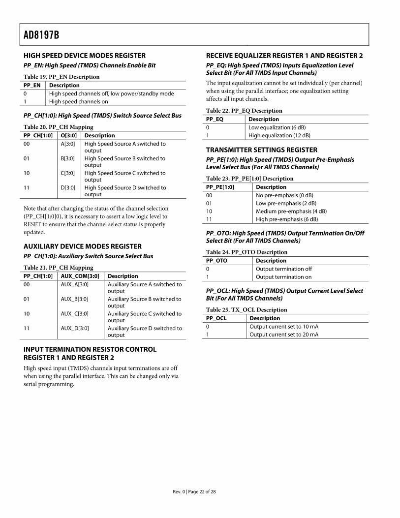
HIGH SPEED DEVICE MODES REGISTER PP_EN: High Speed (TMDS) Channels Enable Bit
Table 19. PP_EN Description PP_EN Description 0 High speed channels off, low power/standby mode 1 High speed channels on
PP_CH[1:0]: High Speed (TMDS) Switch Source Select Bus
Table 20. PP_CH Mapping PP_CH[1:0] O[3:0] Description 00 A[3:0] High Speed Source A switched to
output 01 B[3:0] High Speed Source B switched to
output 10 C[3:0] High Speed Source C switched to
output 11 D[3:0] High Speed Source D switched to
output
Note that after changing the status of the channel selection (PP_CH[1:0]0), it is necessary to assert a low logic level to RESET to ensure that the channel select status is properly updated.
AUXILIARY DEVICE MODES REGISTER PP_CH[1:0]: Auxiliary Switch Source Select Bus
Table 21. PP_CH Mapping PP_CH[1:0] AUX_COM[3:0] Description 00 AUX_A[3:0] Auxiliary Source A switched to
output 01 AUX_B[3:0] Auxiliary Source B switched to
output 10 AUX_C[3:0] Auxiliary Source C switched to
output 11 AUX_D[3:0] Auxiliary Source D switched to
output
INPUT TERMINATION RESISTOR CONTROL REGISTER 1 AND REGISTER 2 High speed input (TMDS) channels input terminations are off when using the parallel interface. This can be changed only via serial programming.
RECEIVE EQUALIZER REGISTER 1 AND REGISTER 2 PP_EQ: High Speed (TMDS) Inputs Equalization Level Select Bit (For All TMDS Input Channels)
The input equalization cannot be set individually (per channel) when using the parallel interface; one equalization setting affects all input channels.
Table 22. PP_EQ Description PP_EQ Description 0 Low equalization (6 dB) 1 High equalization (12 dB)
TRANSMITTER SETTINGS REGISTER PP_PE[1:0]: High Speed (TMDS) Output Pre-Emphasis Level Select Bus (For All TMDS Channels)
Table 23. PP_PE[1:0] Description PP_PE[1:0] Description 00 No pre-emphasis (0 dB) 01 Low pre-emphasis (2 dB) 10 Medium pre-emphasis (4 dB) 11 High pre-emphasis (6 dB)
PP_OTO: High Speed (TMDS) Output Termination On/Off Select Bit (For All TMDS Channels)
Table 24. PP_OTO Description PP_OTO Description 0 Output termination off 1 Output termination on
PP_OCL: High Speed (TMDS) Output Current Level Select Bit (For All TMDS Channels)
Table 25. TX_OCL Description PP_OCL Description 0 Output current set to 10 mA 1 Output current set to 20 mA
AD8197B
Rev. 0 | Page 23 of 28
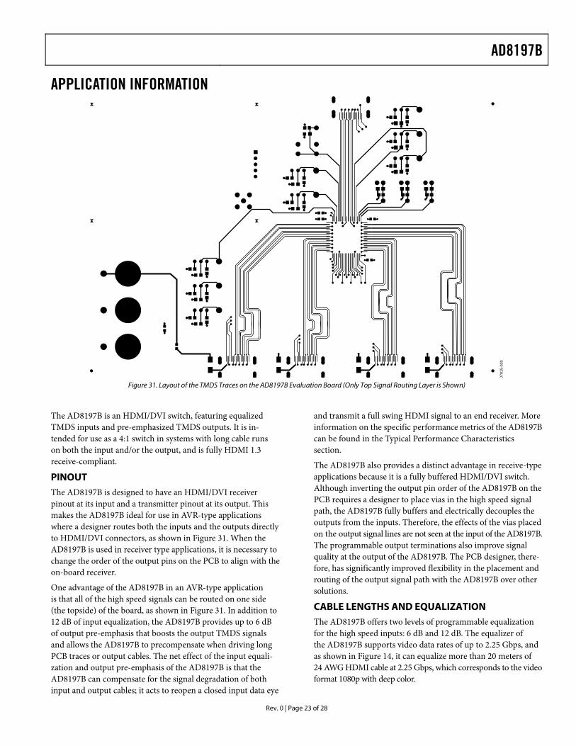
APPLICATION INFORMATION
0701
5-03
0
Figure 31. Layout of the TMDS Traces on the AD8197B Evaluation Board (Only Top Signal Routing Layer is Shown)
The AD8197B is an HDMI/DVI switch, featuring equalized TMDS inputs and pre-emphasized TMDS outputs. It is in-tended for use as a 4:1 switch in systems with long cable runs on both the input and/or the output, and is fully HDMI 1.3 receive-compliant.
PINOUT The AD8197B is designed to have an HDMI/DVI receiver pinout at its input and a transmitter pinout at its output. This makes the AD8197B ideal for use in AVR-type applications where a designer routes both the inputs and the outputs directly to HDMI/DVI connectors, as shown in Figure 31. When the AD8197B is used in receiver type applications, it is necessary to change the order of the output pins on the PCB to align with the on-board receiver.
One advantage of the AD8197B in an AVR-type application is that all of the high speed signals can be routed on one side (the topside) of the board, as shown in Figure 31. In addition to 12 dB of input equalization, the AD8197B provides up to 6 dB of output pre-emphasis that boosts the output TMDS signals and allows the AD8197B to precompensate when driving long PCB traces or output cables. The net effect of the input equali-zation and output pre-emphasis of the AD8197B is that the AD8197B can compensate for the signal degradation of both input and output cables; it acts to reopen a closed input data eye
and transmit a full swing HDMI signal to an end receiver. More information on the specific performance metrics of the AD8197B can be found in the Typical Performance Characteristics section.
The AD8197B also provides a distinct advantage in receive-type applications because it is a fully buffered HDMI/DVI switch. Although inverting the output pin order of the AD8197B on the PCB requires a designer to place vias in the high speed signal path, the AD8197B fully buffers and electrically decouples the outputs from the inputs. Therefore, the effects of the vias placed on the output signal lines are not seen at the input of the AD8197B. The programmable output terminations also improve signal quality at the output of the AD8197B. The PCB designer, there-fore, has significantly improved flexibility in the placement and routing of the output signal path with the AD8197B over other solutions.
CABLE LENGTHS AND EQUALIZATION The AD8197B offers two levels of programmable equalization for the high speed inputs: 6 dB and 12 dB. The equalizer of the AD8197B supports video data rates of up to 2.25 Gbps, and as shown in Figure 14, it can equalize more than 20 meters of 24 AWG HDMI cable at 2.25 Gbps, which corresponds to the video format 1080p with deep color.
AD8197B
Rev. 0 | Page 24 of 28
The length of cable that can be used in a typical HDMI/DVI application depends on a large number of factors, including:
• Cable quality: the quality of the cable in terms of conductor wire gauge and shielding. Thicker conductors have lower signal degradation per unit length.
• Data rate: the data rate being sent over the cable. The signal degradation of HDMI cables increases with data rate.
• Edge rates: the edge rates of the source input. Slower input edges result in more significant data eye closure at the end of a cable.
• Receiver sensitivity: the sensitivity of the terminating receiver.
As such, specific cable types and lengths are not recommended for use with a particular equalizer setting. In nearly all applica-tions, the AD8197B equalization level can be set to high, or 12 dB, for all input cable configurations at all data rates, without degrading the signal integrity.
PCB LAYOUT GUIDELINES The AD8197B is used to switch two distinctly different types of signals, both of which are required for HDMI and DVI video. These signal groups require different treatment when laying out a PC board.
The first group of signals carries the audiovisual (AV) data. HDMI/DVI video signals are differential, unidirectional, and high speed (up to 2.25 Gbps). The channels that carry the video data must be controlled impedance, terminated at the receiver, and capable of operating at the maximum specified system data rate. It is especially important to note that the differential traces that carry the TMDS signals should be designed with a controlled differential impedance of 100 Ω. The AD8197B provides single-ended, 50 Ω terminations on-chip for both its inputs and outputs, and both the input and output terminations can be enabled or disabled through the serial control interface. The output termi-nations can also be enabled or disabled through the parallel control interface. Transmitter termination is not required by the HDMI 1.3 standard, but its inclusion improves the overall system signal integrity.
The audiovisual (AV) data carried on these high speed channels is encoded by a technique called transmission minimized differ-ential signaling (TMDS) and in the case of HDMI, is also encrypted according to the high bandwidth digital copy protection (HDCP) standard.
The second group of signals consists of low speed auxiliary control signals used for communication between a source and a sink. Depending upon the application, these signals can include the DDC bus (this is an I2C bus used to send EDID information and HDCP encryption keys between the source and the sink), the consumer electronics control (CEC) line, and the hot plug detect (HPD) line. These auxiliary signals are bidirectional, low speed, and transferred over a single-ended transmission line that does not need to have controlled impedance. The primary
concern with laying out the auxiliary lines is ensuring that they conform to the I2C bus standard and do not have excessive capacitive loading.
TMDS Signals
In the HDMI/DVI standard, four differential pairs carry the TMDS signals. In DVI, three of these pairs are dedicated to carrying RGB video and sync data. For HDMI, audio data is interleaved with the video data; the DVI standard does not incorporate audio information. The fourth high speed differ-ential pair is used for the AV data-word clock and runs at one-tenth the speed of the TMDS data channels.
The four high speed channels of the AD8197B are identical. No concession was made to lower the bandwidth of the fourth channel for the pixel clock, so any channel can be used for any TMDS signal. The user chooses which signal is routed over which channel. Additionally, the TMDS channels are symmetrical; therefore, the p and n of a given differential pair are inter-changeable, provided the inversion is consistent across all inputs and outputs of the AD8197B. However, the routing between inputs and outputs through the AD8197B is fixed. For example, Output Channel 0 always switches between Input A0, Input B0, Input C0, Input D0, and so forth.
The AD8197B buffers the TMDS signals and the input traces can be considered electrically independent of the output traces. In most applications, the quality of the signal on the input TMDS traces is more sensitive to the PCB layout. Regardless of the data being carried on a specific TMDS channel, or whether the TMDS line is at the input or the output of the AD8197B, all four high speed signals should be routed on a PCB in accor-dance with the same RF layout guidelines.
Layout for the TMDS Signals
The TMDS differential pairs can be either microstrip traces, routed on the outer layer of a board, or stripline traces, routed on an internal layer of the board. If microstrip traces are used, there should be a continuous reference plane on the PCB layer directly below the traces. If stripline traces are used, they must be sandwiched between two continuous reference planes in the PCB stack-up. Additionally, the p and n of each differential pair must have a controlled differential impedance of 100 Ω. The characteristic impedance of a differential pair is a function of several variables including the trace width, the distance separating the two traces, the spacing between the traces and the reference plane, and the dielectric constant of the PC board binder material. Interlayer vias introduce impedance discontinuities that can cause reflections and jitter on the signal path, therefore, it is preferable to route the TMDS lines exclusively on one layer of the board, particularly for the input traces. In some applications, such as using multiple AD8197Bs to construct large input arrays, the use of interlayer vias becomes unavoidable. In these situations, the input termination feature of the AD8197B improves system signal integrity by absorbing reflections. Take care to use vias minimally and to place vias symmetrically for each side of a given differential pair. Furthermore, to prevent unwanted signal coupling and
AD8197B
Rev. 0 | Page 25 of 28
interference, route the TMDS signals away from other signals and noise sources on the PCB.
Both traces of a given differential pair must be equal in length to minimize intrapair skew. Maintaining the physical symmetry of a differential pair is integral to ensuring its signal integrity; excessive intrapair skew can introduce jitter through duty cycle distortion (DCD). The p and n of a given differential pair should always be routed together to establish the required 100 Ω differ-ential impedance. Enough space should be left between the differential pairs of a given group so that the n of one pair does not couple to the p of another pair. For example, one technique is to make the interpair distance 4 to 10 times wider than the intrapair spacing.
Any group of four TMDS channels (Input A, Input B, Input C, Input D, or the output) should have closely matched trace lengths to minimize interpair skew. Severe interpair skew can cause the data on the four different channels of a group to arrive out of alignment with one another. A good practice is to match the trace lengths for a given group of four channels to within 0.05 inches on FR4 material.
Minimizing intrapair and interpair skew becomes increasingly important as data rates increase. Any introduced skew consti-tutes a correspondingly larger fraction of a bit period at higher data rates.
Though the AD8197B features input equalization and output pre-emphasis, the length of the TMDS traces should be minimized to reduce overall signal degradation. Commonly used PC board material such as FR4 is lossy at high frequencies; therefore, long traces on the circuit board increase signal attenuation resulting in decreased signal swing and increased jitter through intersymbol interference (ISI).
Controlling the Characteristic Impedance of a TMDS Differential Pair
The characteristic impedance of a differential pair depends on a number of variables, including the trace width, the distance between the two traces, the height of the dielectric material between the trace and the reference plane below it, and the dielectric constant of the PCB binder material. To a lesser extent, the characteristic impedance also depends upon the trace thickness and the presence of solder mask. There are many combinations that can produce the correct characteristic impedance. Generally, working with the PC board fabricator is required to obtain a set of parameters to produce the desired results.
One consideration is how to guarantee a differential pair with a differential impedance of 100 Ω over the entire length of the trace. One technique to accomplish this is to change the width of the traces in a differential pair based on how closely one trace is coupled to the other. When the two traces of a differential pair are close and strongly coupled, they should have a width that produces a 100 Ω differential impedance. When the traces split apart, to go into a connector, for example, and are no
longer so strongly coupled, the width of the traces should be increased to yield a differential impedance of 100 Ω in the new configuration.
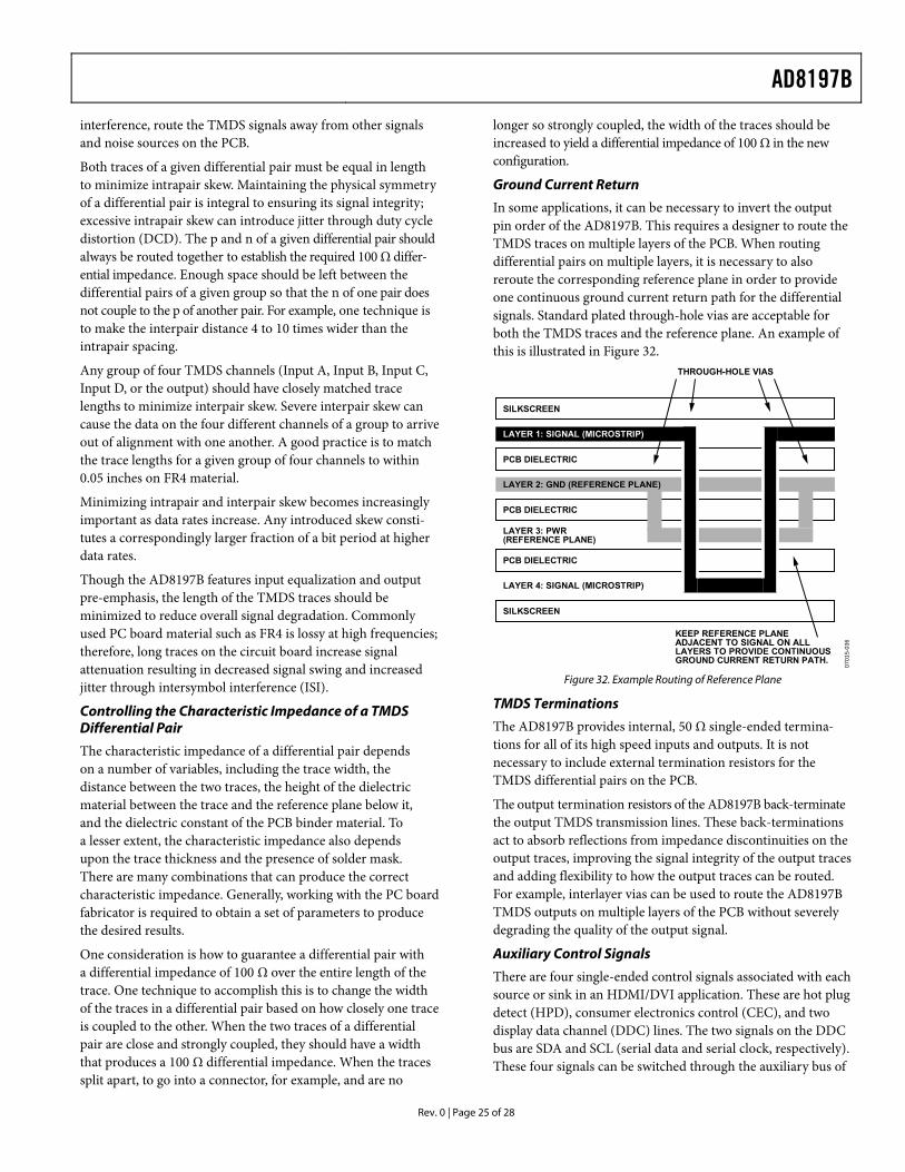
Ground Current Return
In some applications, it can be necessary to invert the output pin order of the AD8197B. This requires a designer to route the TMDS traces on multiple layers of the PCB. When routing differential pairs on multiple layers, it is necessary to also reroute the corresponding reference plane in order to provide one continuous ground current return path for the differential signals. Standard plated through-hole vias are acceptable for both the TMDS traces and the reference plane. An example of this is illustrated in Figure 32.
PCB DIELECTRIC
SILKSCREEN
SILKSCREEN
PCB DIELECTRIC
PCB DIELECTRIC
LAYER 2: GND (REFERENCE PLANE)
LAYER 4: SIGNAL (MICROSTRIP)
THROUGH-HOLE VIAS
LAYER 1: SIGNAL (MICROSTRIP)
KEEP REFERENCE PLANEADJACENT TO SIGNAL ON ALLLAYERS TO PROVIDE CONTINUOUSGROUND CURRENT RETURN PATH.
LAYER 3: PWR(REFERENCE PLANE)
0701
5-03
6
Figure 32. Example Routing of Reference Plane
TMDS Terminations
The AD8197B provides internal, 50 Ω single-ended termina-tions for all of its high speed inputs and outputs. It is not necessary to include external termination resistors for the TMDS differential pairs on the PCB.
The output termination resistors of the AD8197B back-terminate the output TMDS transmission lines. These back-terminations act to absorb reflections from impedance discontinuities on the output traces, improving the signal integrity of the output traces and adding flexibility to how the output traces can be routed. For example, interlayer vias can be used to route the AD8197B TMDS outputs on multiple layers of the PCB without severely degrading the quality of the output signal.
Auxiliary Control Signals
There are four single-ended control signals associated with each source or sink in an HDMI/DVI application. These are hot plug detect (HPD), consumer electronics control (CEC), and two display data channel (DDC) lines. The two signals on the DDC bus are SDA and SCL (serial data and serial clock, respectively). These four signals can be switched through the auxiliary bus of
AD8197B
Rev. 0 | Page 26 of 28
the AD8197B and do not need to be routed with the same strict considerations as the high speed TMDS signals.
In general, it is sufficient to route each auxiliary signal as a single-ended trace. These signals are not sensitive to impedance discontinuities, do not require a reference plane, and can be routed on multiple layers of the PCB. However, it is best to follow strict layout practices whenever possible to prevent the PCB design from affecting the overall application. The specific routing of the HPD, CEC, and DDC lines depends upon the application in which the AD8197B is being used.
For example, the maximum speed of signals present on the auxiliary lines is 100 kHz I2C data on the DDC lines; therefore, any layout that enables 100 kHz I2C to be passed over the DDC bus should suffice. The HDMI 1.3 specification, however, places a strict 50 pF limit on the amount of capacitance that can be measured on either SDA or SCL at the HDMI input connector. This 50 pF limit includes the HDMI connector, the PCB, and whatever capacitance is seen at the input of the AD8197B, or an equivalent receiver. There is a similar limit of 100 pF of input capacitance for the CEC line.
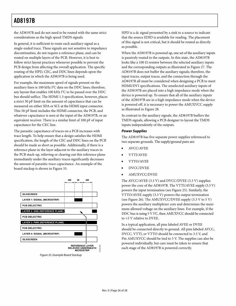
The parasitic capacitance of traces on a PCB increases with trace length. To help ensure that a design satisfies the HDMI specification, the length of the CEC and DDC lines on the PCB should be made as short as possible. Additionally, if there is a reference plane in the layer adjacent to the auxiliary traces in the PCB stack-up, relieving or clearing out this reference plane immediately under the auxiliary traces significantly decreases the amount of parasitic trace capacitance. An example of the board stackup is shown in Figure 33.
PCB DIELECTRIC
LAYER 1: SIGNAL (MICROSTRIP)
SILKSCREEN
SILKSCREEN
PCB DIELECTRIC
PCB DIELECTRIC
LAYER 2: GND (REFERENCE PLANE)
LAYER 3: PWR (REFERENCE PLANE)
LAYER 4: SIGNAL (MICROSTRIP)
W3W 3W
REFERENCE LAYERRELIEVED UNDERNEATH
MICROSTRIP 0701
5-03
2
Figure 33. Example Board Stackup
HPD is a dc signal presented by a sink to a source to indicate that the source EDID is available for reading. The placement of this signal is not critical, but it should be routed as directly as possible.
When the AD8197B is powered up, one set of the auxiliary inputs is passively routed to the outputs. In this state, the AD8197B looks like a 100 Ω resistor between the selected auxiliary inputs and the corresponding outputs as illustrated in Figure 27. The AD8197B does not buffer the auxiliary signals; therefore, the input traces, output traces, and the connection through the AD8197B all must be considered when designing a PCB to meet HDMI/DVI specifications. The unselected auxiliary inputs of the AD8197B are placed into a high impedance mode when the device is powered up. To ensure that all of the auxiliary inputs of the AD8197B are in a high impedance mode when the device is powered off, it is necessary to power the AMUXVCC supply as illustrated in Figure 28.
In contrast to the auxiliary signals, the AD8197B buffers the TMDS signals, allowing a PCB designer to layout the TMDS inputs independently of the outputs.
Power Supplies
The AD8197B has five separate power supplies referenced to two separate grounds. The supply/ground pairs are:
• AVCC/AVEE
• VTTI/AVEE
• VTTO/AVEE
• DVCC/DVEE
• AMUXVCC/DVEE
The AVCC/AVEE (3.3 V) and DVCC/DVEE (3.3 V) supplies power the core of the AD8197B. The VTTI/AVEE supply (3.3 V) powers the input termination (see Figure 25). Similarly, the VTTO/AVEE supply (3.3 V) powers the output termination (see Figure 26). The AMUXVCC/DVEE supply (3.3 V to 5 V) powers the auxiliary multiplexer core and determines the maxi-mum allowed voltage on the auxiliary lines. For example, if the DDC bus is using 5 V I2C, then AMUXVCC should be connected to +5 V relative to DVEE.
In a typical application, all pins labeled AVEE or DVEE should be connected directly to ground. All pins labeled AVCC, DVCC, VTTI, or VTTO should be connected to 3.3 V, and Pin AMUXVCC should be tied to 5 V. The supplies can also be powered individually, but care must be taken to ensure that each stage of the AD8197B is powered correctly.
AD8197B
Rev. 0 | Page 27 of 28
Power Supply Bypassing
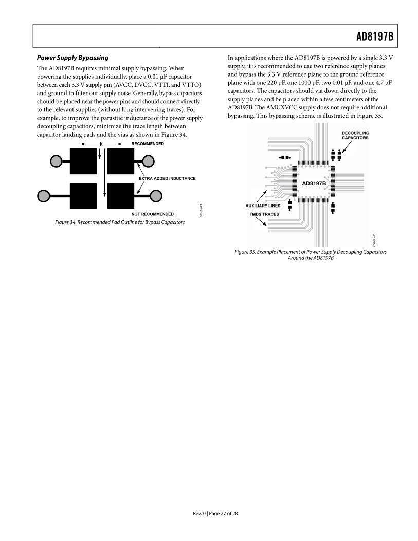
The AD8197B requires minimal supply bypassing. When powering the supplies individually, place a 0.01 μF capacitor between each 3.3 V supply pin (AVCC, DVCC, VTTI, and VTTO) and ground to filter out supply noise. Generally, bypass capacitors should be placed near the power pins and should connect directly to the relevant supplies (without long intervening traces). For example, to improve the parasitic inductance of the power supply decoupling capacitors, minimize the trace length between capacitor landing pads and the vias as shown in Figure 34.
EXTRA ADDED INDUCTANCE
RECOMMENDED
NOT RECOMMENDED 0701
5-03
3
Figure 34. Recommended Pad Outline for Bypass Capacitors
In applications where the AD8197B is powered by a single 3.3 V supply, it is recommended to use two reference supply planes and bypass the 3.3 V reference plane to the ground reference plane with one 220 pF, one 1000 pF, two 0.01 μF, and one 4.7 μF capacitors. The capacitors should via down directly to the supply planes and be placed within a few centimeters of the AD8197B. The AMUXVCC supply does not require additional bypassing. This bypassing scheme is illustrated in Figure 35.
AD8197B
0701
5-03
4
Figure 35. Example Placement of Power Supply Decoupling Capacitors
Around the AD8197B
AD8197B
Rev. 0 | Page 28 of 28
OUTLINE DIMENSIONS
COMPLIANT TO JEDEC STANDARDS MS-026-BED
TOP VIEW(PINS DOWN)
1
2526
5150
7576100
0.50BSC
LEAD PITCH
0.270.220.17
1.60 MAX
0.750.600.45
VIEW A
PIN 1
1.451.401.35
0.150.05
0.200.09
0.08COPLANARITY
VIEW AROTATED 90° CCW
SEATINGPLANE
7°3.5°0°
14.2014.00 SQ13.80
16.2016.00 SQ15.80
0517
06-A
Figure 36. 100-Lead Low Profile Quad Flat Package [LQFP]
(ST-100) Dimensions shown in millimeters
ORDERING GUIDE Model Temperature Range Package Description Package Option Ordering Quantity AD8197BASTZ1 −40°C to +85°C 100-Lead Low Profile Quad Flat Package [LQFP] ST-100 AD8197BASTZ-RL1 −40°C to +85°C 100-Lead Low Profile Quad Flat Package [LQFP] ST-100 1,000 AD8197B-EVALZ1 Evaluation Board 1 Z = RoHS Compliant Part.
©2008 Analog Devices, Inc. All rights reserved. Trademarks and registered trademarks are the property of their respective owners. D07015-0-1/08(0)