Embed Size (px)
Citation preview
AD-A.24 3 713
IC~
~O
~6PART POR'CE
"W ~ f p~,i isOn 1 10 r
AFIT/GE/ENG/91D-55
r4$
Evaluation of an InterdigitatedGate Electrode Field-Effect Transistor (IGEFET)
for In Situ Resin Cure Monitoring
THESIS
Thomas E. Graham
Captain, USAF
AFIT/GE/ENG/91D-55
Thi do,7uPmclil hO.; k~~.C:r'(
Approved for public release; distribution unlimited
91-19027 91 1224 0641111liol
AFIT/GE/ENG/91D-55
Evaluation of an Interdigitated Gate Electrode Field-Effect Transistor (IGEFET)
for In Situ Resin Cure Monitoring
THESIS
Presented to the Faculty of the School of Engineering
of the Air Force Institute of Technology
Air University
In Partial Fulfillment of the
Requirements for the Degree of
Master of Science in Electrical Engineering
Thomas E. Graham, B.S.E.E.
Captain, USAF -------
15 November 1991
Approved for public release; distribution unlimited
Acknowledgments
This thesis has been the most ambitious undertaking of my life. Without the knowledge,
help, and support of several individuals, this thesis would not have been possible. I deeply
appreciate the assistance I received.
I am grateful to my advisor, Lt Col Edward Kolesar, for his patience and his positive
attitude. His continual interest in my work kept me going when little else would. I owe Ms
Francis Abrams at the Wright Research and Development Center's Non-Metallic Materials
Laboratory thanks for making her personnel, equipment, and expertise available to me. I also owe
a debt of gratitude to Capt John Wiseman and Capt Thomas Jenkins for their advice and
assistance, and to Capt Anthony Moosey, Capt Rocky Weston, and Capt Charles Brothers for
their moral support. I would also like to thank the AFIT Electronics and Materials Cooperative
Laboratory Staff for their help with the facilities and equipment used in this thesis.
Finally, I would like to thank my wife, Marisa, and my son, Chistopher for their love,
understanding, and support through this experience.
Thomas E. Graham
ii
Table of Contents
Page
Acknowledgments..... ..... .. .. .. .. .. .. .. .. .. .. .. .. .. .. . ....
Table of Contents..... .... .. .. .. .. .. .. .. .. .. .. .. .. .. .. . . .....
List of Figures .. .. .. .. ... .. ... ... ... .. ... ... .. ... ... ....... iv
List of Tables. .. .. .. .. .. ... ... .. ... ... .. ... ... ... .. ... .... x
Abstract .. .. .. .. .. .. ... ... .. ... ... ... .. ... ... ... .. ...... xi
1. Introduction .. .. .. .. .. .. ... ... .. ... ... .. ... ... ... ..... 1-1
Background .. .. .. .. ... .. ... ... ... .. ... ... ... ..... 1-1
Problem Statement .. .. .. .. .. ... ... .. ... ... ... .. ..... 1-4
Justification. .. .. .. .. ... ... ... .. ... ... ... ..... 1-4
Scope. .. .. .. .. ... .. ... ... .. ... ... ... .. ..... 1-4
Definitions .. .. .. .. .. ... ... ... .. ... ... ... ..... 1-5
Approach. .. .. .. .. .. ... .. ... ... .. ... ... ... .. ..... 1-6
IGEFET Redesign .. .. .. .. .. ... .. ... ... ... .. ..... 1-6
IGEFET Qualification. .. .. .. .. .. ... .. ... ... ... .... 1-8
Performance Data Collection. .. .. .. .. .. ... ... ... ..... 1-9
Experimental Data Reduction. .. .. .. .. ... ... ... ...... 1-10
Plan of Development .. .. .. .. ... .. ... ... ... .. ... ...... 1-10
11. Literature Review of Sensors for In Situ Resin Cure Monitoring. .. .. .. .. .... 2-1
Introduction. .. .. .. .. ... .. ... ... .. ... ... ... .. ..... 2-1
Fluorescence Sensors. .. .. .. .. ... ... .. ... ... ... .. ..... 2-1
Fluorescence Monitoring with an Internal Standard. .. .. .. ..... 2-1
Fluorescence Monitoring with Reactive Dye Labels. .. .. .. .. .... 2-2
iii
Page
Electrical Sensors. .. .. .. .. ... .. ... ... ... .. ... ... ... 2-2
Dynamic Dielectric Analysis. .. .. .. .. ... ... ... .. ..... 2-2
Chemiresistor. .. .. .. .. .. .. ... ... ... .. ... ... ... 2-3
Metal-Oxide-Semiconductor (MOS)-Based Sensors. .. .. .. .. .... 2-4
Summary .. .. .. .. .. .. ... ... .. ... ... .. ... ... ...... 2-15
111. Theory of IGEFET Resin Cure Monitoring .. .. .. .. ... .. ... ... ..... 3-1
Introduction. .. .. .. .. .. ... ... ... .. ... ... ... .. ..... 3-1
Polarization Mechanismfs in Dielectric Materials .. .. .. .. .. ... ..... 3-1
Electronic Polarization. .. .. .. .. ... ... ... .. ... ..... 3-1
Atomic Polarization. .. .. .. .. .. ... ... ... .. ... ..... 3-2
Orientational Polarization. .. .. .. .. .. .. ... ... ... ..... 3-2
Interfacial Polarization. .. .. .. .. ... ... ... .. ... ..... 3-3
Dielectric Relaxation. .. .. .. .. ... .. ... ... ... .. ... ..... 3-3
Complex Permittivity .. .. .. .. .. ... ... .. ... ... ..... 3-4
Debye Equations. .. .. .. .. .. ... .. ... ... ... .. ..... 3-6
Cole-Cole Model. .. .. .. .. .. ... ... ... .. ... ... ... 3-10
Epoxy Resin Systems .. .. .. .. .. ... .. ... ... ... .. ... ... 3-11
Gelation Point .. .. .. .. .. ... ... .. ... ... ... .. ... 3-16
Glass Transition Temperature. .. .. .. ... .. ... ... ...... 3-16
Viscosity .. .. .. .. .. ... ... ... .. ... ... ... .. ... 3-17
Equivalent Circuit Representation of the IGEFET-Resin System. .. .. ... 3-18
Summary .. .. .. .. .. .. ... .. ... ... ... .. ... ... ...... 3-20
IV. IGEFET Sensor Design, Instrumentation Configuration, and Experimental Method-
ology. .. .. .. .. .. ... .. ... ... .. ... ... ... .. ... ... ..... 4-1
IGEFET Sensor Design and Characterization .. .. .. .. ... ... ..... 4-1
Design Goals .. .. .. .. .. ... .. ... ... ... .. ... ..... 4-1
Interdigitated Gate Electrode Structure Design .. .. .. .. .. ..... 4-2
iv
Page
Sensor Element Amplifier Design .......................... 4-4
Reference Element Design .............................. 4-6
Multiplexer and Demultiplexer Circuit Designs ................ 4-6
Voltage Follower Circuit Design ...... .................... 4-9
Operational Amplifier Circuit Design ..... ................. 4-9
Final Design ....... ............................... 4-9
IGEFET Integrated Circuit Fabrication ..................... 4-15
IG EFET Performance Instrumentation Configuration ................ 4-19
General Considerations ...... ......................... 4-19
Electrical Performance Instrumentation Configurations .......... 4-23
Experimental Methodology ................................. 4-31
Mechanical Test Procedures ............................ 4-31
IGEFET Test Procedures .............................. 4-33
Summary ............................................ 4-37
V. Results and Discussion ........................................ 5-1
Introduction ........ ................................... 5-1
Electrical Characteristics of the IGEFET Sensor ................... 5-1
Mechanical Characterization of the Resin ........................ 5-5
Parallel Plate Measurements with a Ramped Temperature Profile 5-5
Parallel Plate Measurements with an Isothermal Temperature Profile 5-6
Torsional Bar Analysis of the Resin ...... .................. 5-9
Resin Cure Experiments ....... ............................ 5-12
Direct Current Resistance of the Interdigitated Gate Electrode Struc-
ture ........ .................................... 5-12
Impedance of the Interdigitated Gate Electrode Structure ...... ... 5-17
Transfer Function of the Interdigitated Gate Electrode Structure . . 5-39
Transfer Function of the IGEFET Sensor ................... 5-47
v
Page
Time-Domain Response of the IGEFET Sensor to a Pulsed Voltage
Excitation Signal.................................. 5-58
Frequency-Domain Response of the IGEFET Sensor to a Pulsed Volt-
age Excitation Signal. .. .. .. .. ... ... .. ... ... ...... 5-63
Summary .. .. .. .. .. .. ... ... .. ... ... ... .. ... ...... 5-69
VI. Conclusions and Recommendations. .. .. .. .. .. ... ... .. ... ... ... 6-1
Conclusions .. .. .. .. ... ... .. ... ... .. ... ... ... ..... 6-i
Recommendations. .. .. .. .. .. ... ... .. ... ... ... .. ..... 6-3
Appendix A. SPICE Simulation Program .. .. .. .. .. .. ... ... .. ... ... A-1
Appendix B. MOSIS Parametric Test Results. .. .. .. .. ... ... .. ... ... B-i
Appendix C. Data Collection Software .. .. .. .. .. ... ... ... .. ... ... C-i
Direct Current Data Collection Program. .. .. .. .. ... ... .. ..... C-i
General Data Collection Program .. .. .. .. .. ... ... .. ... ..... C-5
Bibliography .. .. .. .. ... .. ... ... ... .. ... ... ... .. ... ... .. BIB-i
Vita. .. .. .. .. ... .. ... ... .. ... ... ... .. ... ... ... .. .... VITA-i
vi
List of Figures
Figure Page
1.1. Illustration of the IGEFET ......... .............................. 1-3
1.2. Block diagram of the IGEFET sensor system ....... .................... 1-7
2.1. Fluorescence intensity (If) at 418 nm as a function of cure time for a resin cured
at two different temperatures ......... ............................. 2-3
2.2. Diagram of the chemiresistor ......... ............................. 2-4
2.3. Diagram of an Ion-Sensitive Field-Effect Transistor (ISFET) ..... ........... 2-5
2.4. A typical charge-flow sensor ......... ............................. 2-6
2.5. Illustration the charge-flow transistor (CFT) ....... .................... 2-7
2. C. Current wavefcns for the Jiarge-flow transistor (CFT) ................... 2-8
2.7. Illustration of the modified charge-flow transistor structure ..... ............ 2-9
2.8. Current waveforms for the modified charge-flow transistor (CFT) ............. 2-9
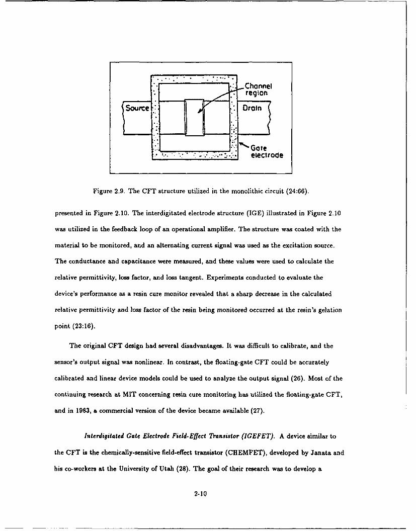
2.9. The charge-flow transistor structure utilized in a monolithic circuit ... ....... 2-10
2.10. Diagram of the floating gate charge-flow transistor ...................... 2-11
2.11. Diagram of the work-function chemically-sensitive field-effect transistor ..... 2-12
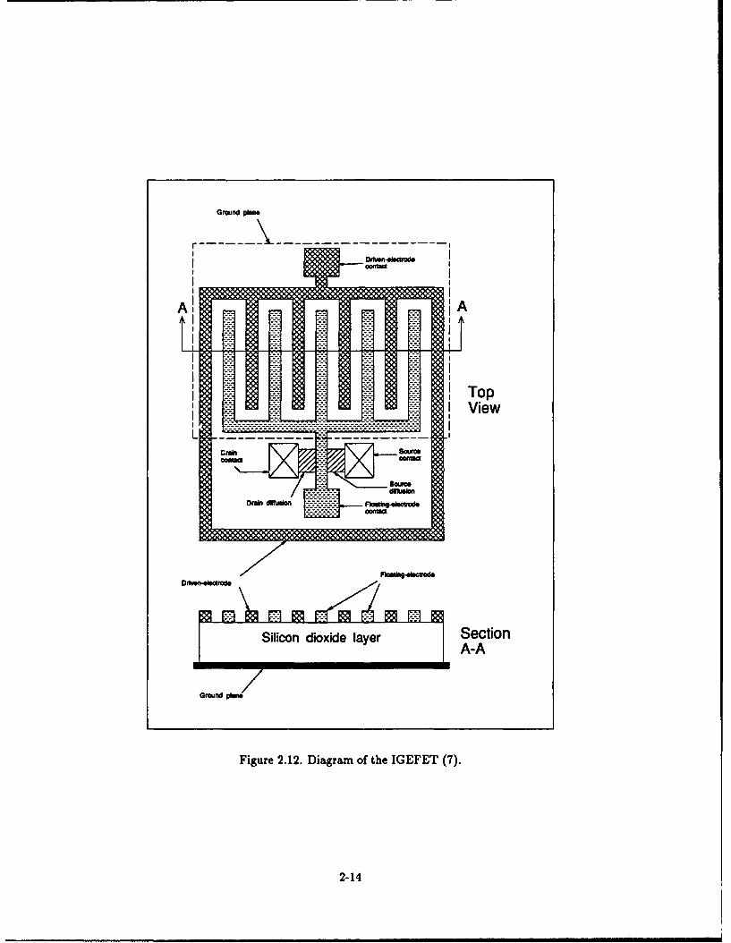
2.12. Diagram of the IGEFET ......... ............................... 2-14
3.1. Mechanisms of polarization ......... .............................. 3-2
3.2. Magnitudes of the four polarization mechanisms with respect to frequency . . . 3-3
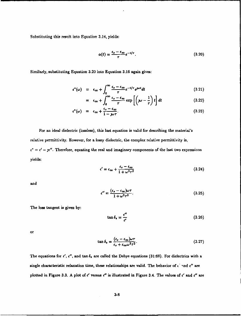
3.3. Real and imaginary components of the complex relative permittivity of a dielectric
as a function of frequency ......... ............................... 3-9
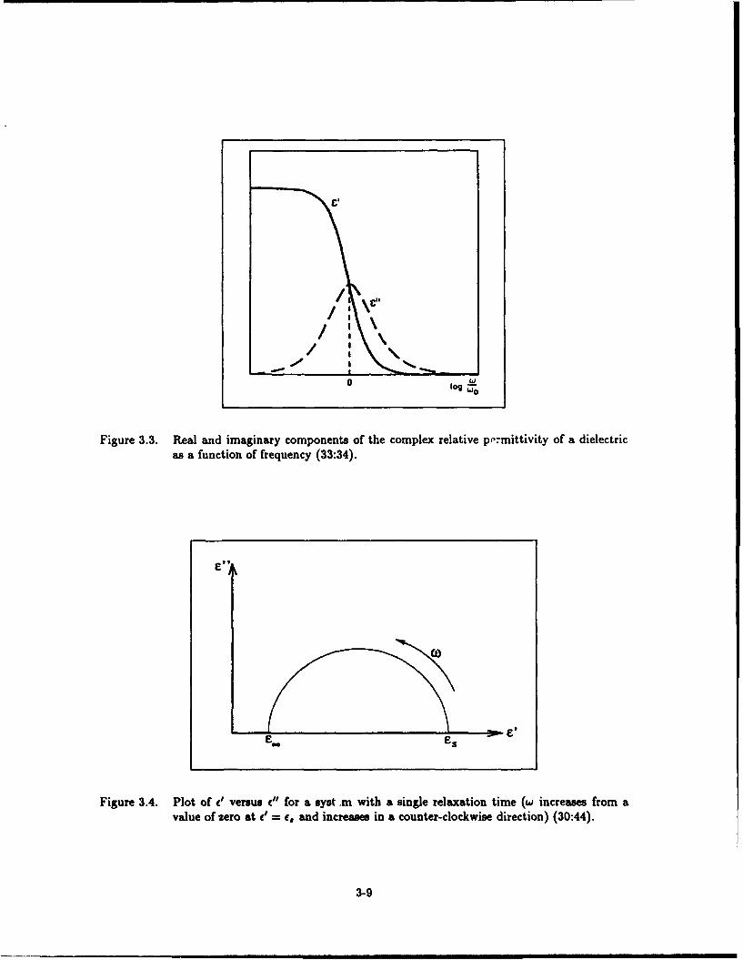
3.4. Plot of c' versus c" for a system with a single relaxation time ............... 3-9
3.5. Cole-Cole plot of a dielectric ......... ............................. 3-11
3.6. The function F(s) describing the distribution of relaxation times for the Cole-Cole
model of complex permittivity ......... ............................ 3-12
3.7. Cole-Cole plot in the impedance plane ....... ........................ 3-12
vii
Figure Page
3.8. Reaction of epichlorohydrin with bisphenol-A to produce the diglycidyl ether of
bisphenol-A (DGEBA) .......... ................................ 3-13
3.9. The cross-linking reaction between DGEBA and a polyamine ............... 3-14
3.10. Time-to-gelation and time-to-vitrication versus isothermal cure temperature for
an epoxy resin .......... ..................................... 3-15
3.11. Real and imaginary components of the shear modulus (G*) as a function of fre-
quency ........... ......................................... 3-18
3.12. A lumped-element equivalent circuit model of the interdigitated gate electrode
(IGE)-resin system .......... ................................... 3-19
4.1. Dimensions of the interdigitated gate electrode structure fingers .... ......... 4-3
4.2. Schematic diagram of the sensor element amplifier ...... ................. 4-4
4.3. Layout of the sensor element amplifier ........ ........................ 4-5
4.4. Schematic diagram of one bit-slice of the logic decoder .................... 4-7
4.5. Schematic diagram of the inverting buffer ........ ...................... 4-8
4.6. Schematic diagram of the transmission switch ...... ................... 4-8
4.7. Layout of the multiplexer and demultiplexer circuits ..................... 4-10
4.8. Schematic diagram of the voltage follower circuit ...... .................. 4-11
4.9. Layout of the voltage follower circuit ........ ........................ 4-12
4.10. Schematic representation of one of the operational amplifier stages ........... 4-13
4.11. Layout of the final IGEFET design depicting the locations of the individual sub-
circuits ........... ......................................... 4-14
4.12. Photomicrograph of the IGEFET integrated circuit ...... ................ 4-16
4.13. Expected gain of the sensor element amplifier ....... .................... 4-18
4.14. Power supply arrangement used for the IGEFET performance data collection 4-21
4.15. Diagram of the IGEFET test cell ........ ........................... 4-22
4.16. IGEFET direct current resistance instrumentation configuration ............. 4-24
4.17. IGEFET impedance instrumentation configuration ...................... 4-25
4.18. IGEFET gain-phase instrumentation configuration ...................... 4-27
viii

Figure Page
4.19. IGEFET time-domain response instrumentation configuration .... .......... 4-28
4.20. IGEFET frequency-domain response instrumentation configuration ... ....... 4-30
4.21. Location and size of the glass cut which exposed the floating-electrode and the
sensor element output lines ......... .............................. 4-34
5.1. Gain and phase delay of the sensor element amplifier at room temperature . . . 5-2
5.2. Complex viscosity of the resin with respect to a ramped temperature profile . . 5-6
5.3. Parallel plate mechanical analysis of a resin sample for a 45 0 C isothermal temper-
ature cure profile ........... .................................... 5-7
5.4. Parallel plate mechanical analysis of a resin sample for a 550 C isothermal temper-
ature cure profile ........... .................................... 5-8
5.5. Torsional bar analysis for a resin sample cured at 45°C ..... .............. 5-10
5.6. Torsional bar analysis for a resin sample cured at 55*C .... .............. 5-11
5.7. Direct current resistance measured with respect to applied bias for a 450 C resin
cure ........... ........................................... 5-12
5.8. Direct current resistance measured with respect to time (2-volt applied bias) for a
45°C resin cure .......... ..................................... 5-13
5.9. Direct current resistance measured with respect to applied bias for a 55*C resin
cure ........... ........................................... 5-15
5.10. Direct current resistance measured with respect to time (2-volt applied bias) for a
55°C resin cure .......... ..................................... 5-16
5.11. Magnitude of the electrical impedance of the interdigitated gate electrode structure
for the first ten minutes of a 45°C cure ....... ....................... 5-18
5.12. Magnitude of the electrical impedance of the interdigitated gate electrode stri, ' re
after the first ten minutes of a 45°C cure ....... ...................... 5-19
5.13. Phase of the electrical impedance of the interdigitated gate electrode structure for
the first ten minutes of a 45*C cure ........ ......................... 5-20
5.14. Phase of the electrical impedance of the interdigitated gate electrode structure
after the first ten minutes of a 45*C cure ....... ...................... 5-21
5.15 Magnitude of the electrical impedance of the interdigitated gate electrode structure
for a 55°C cure .......... ..................................... 5-22
ix
Figure Page
5.16. Phase of the electrical impedance of the interdigitated gate electrode structure for
a 55°C cure .......... ....................................... 5-23
5.17. Real component of the electrical impedance of the interdigitated gate electrode
structure for the first 10 minutes of a 45*C cure ...... .................. 5-25
5.18. Real component of the electrical impedance of the interdigitated gate electrode
structure after the first 10 minutes of a 450C cure ..... ................. 5-26
5.19. Imaginary component of the electrical impedance of the interdigitated gate elec-
trode structure for the first 10 minutes of a 450C cure ..... ............... 5-27
5.20. Imaginary component of the electrical impedance of the interdigitated gate elec-
trode structure after the first 10 minutes of a 45 0 C cure ..... .............. 5-28
5.21. Real component of the electrical impedance of the interdigitated gate electrode
structure for a 55 0 C cure ......... ............................... 5-29
5.22. Imaginary component of the impedance of the interdigitated gate electrode struc-
ture for a 55°C cure .......... .................................. 5-30
5.23. Cole-Cole representation of the electrical impedance of the interdigitated gate
electrode structure 5 minutes into a 450C cure cycle ...... ................ 5-31
5.24. Cole-Cole representation of the electrical impedance of the interdigitated gate
electrode structure 9 minutes into a 45°C cure cycle ...... ................ 5-32
5.25. Cole-Cole representation of the electrical impedance of the interdigitated gate
electrode structure 14 minutes into a 450C cure cycle ..... ............... 5-33
5.26. Cole-Cole representation of the electrical impedance of the interdigitated gate
electrode structure 2 minutes into a 550C cure cycle ...... ................ 5-35
5.27. Cole-Cole representation of the electrical impedance of the interdigitated gate
electrode structure 10 minutes into a 55°C cure cycle ..... ............... 5-36
5.28. Cole-Cole representation of the electrical impedance of the interdigitated gate
electrode structure 30 minutes into a 55°C cure cycle ..... ............... 5-37
5.29. Cole-Cole representation of the electrical impedance of the interdigitated gate
electrode structure 60 minutes into a 55*C cure cycle ..... ............... 5-38
5.30. Gain of the IGE structure with respect to frequency for a sample cured at 450C 5-40
5.31. Phase delay of the IGE structure with respect to frequency for a sample cured at
450C ............ .......................................... 5-41
x
Figure Page
5.32. Gain and phase delay of the IGE structure with respect to time (frequency equal
to 10 Hz) for a sample cured at 450 C ........ ........................ 5-42
5.33. Equivalent circuit model of the IGE structure ...... ................... 5-43
5.34. Gain of the IGE structure with respect to frequency for a sample cured at 550C 5-44
5.35. Phase delay of the IGE structure with respect to frequency for a sample cured at
55C ............. .......................................... 5-45
5.36. Gain and phase delay of the IGE structure with respect to time (frequency equal
to 10 Hz) for a sample cured at 550C ........ ........................ 5-46
5.37. Gain of the IGE structure with respect to time (frequency equal to 10 Hz) for
samples cured at 450C and 550C ............ ........................... 5-48
5.38. Phase delay of the IGE structure with respect to time (frequency equal to 10 Hz)
for samples cured at 45 0 C and 550C ........ ......................... 5-49
5.39. Gain of the IGEFET sensor with respect to frequency for a sample cured at 450C 5-50
5.40. Phase delay of the IGEFET sensor with respect to frequency for a sample cured
at 450C ............. ......................................... ..... 5-51
5.41. Gain and phase delay of the IGEFET sensor with respect to time (frequency equal
to 10 Hz) for a sample cured at 45C ........ ........................ 5-52
5.42. Gain of the IGEFET sensor with respect to frequency for a sample cured at 550C 5-53
5.43. Phase delay of the IGEFET sensor with respect to frequency for a sample cured
at 550C ........... ......................................... 5-54
5.44. Gain and phase delay of the IGEFET sensor with respect to time (frequency equal
to 10 Hz) for a sample cured at 550C ........ ........................ ..... 5-55
5.45. Gain of the IGEFET sensor with respect to time (frequency equal to 10 Hz) for
samples cured at 450C and 550C ........ ........................... ..... 5-56
5.46. Phase delay of the IGEFET sensor with respect to time (frequency equal to 10
Hz) for samples cured at 45*C and 550C ...... ...................... ..... 5-57
5.47. Excitation pulse uw~d for the time-domain response measurements (a 40-psec wide
window is illustrated) .......... ................................. 5-59
5.48. Time-domain response of the IGEFET sensor for the first 10 minutes of a 450C
cure cycle (a 40-psec wide window is illustrated) ...... .................. 5-60
xi
Figure Page
5.49. Time-domain response of the IGEFET sensor after the first 10 minutes of a 450C
cure cycle (a 40-pjsec wide window is illustrated) ....................... 5-61
5.50. Time-domain response of the IGEFET sensor for a 55*C cure cycle (a 40 /ssec
wide window is illustrated) ....... .............................. 5-62
5.51. Normalized Fourier transform of the input signal used in the frequency-domain
analysis ........ ......................................... 5-64
5.52. Normalized Fourier transform spectrum for the reference element at 450C . . . . 5-65
5.53. Normalized difference Fourier transform magnitude spectra for a 45C cure . . . 5-66
5.54. Normalized Fourier transform spectrum for the reference element at 55*C . . . . 5-67
5.55. Normalized difference Fourier transform magnitude spectra for a 550C cure . . . 5-68
xii
List of Tables
Table Page
1.1. Electrical measurements .. .. .. .. .. .. ... ... .. ... ... ... .. ... 1-10
1.2. Mechanical measurements. .. .. .. .. .. .. ... ... ... .. ... ... ... 1-11
4.1. IGEFET integrated circuit pin assignments .. .. .. ... .. ... ... ...... 4-17
xiii
AFIT/GE/ENG/91D-55
Abstract
The purpose of this study was to design an Interdigitated Gate Electrode Field-Effect
Transistor (IGEFET) and evaluate its performance as an in situ resin cure monitor. A
commercially available resin was selected for the research, and rheological studies were performed
to establish the optimal range of cure temperatures. Additional rheological studies were performed
to identify the resin's gelation point during isothermal cures at two selected temperatures, and to
determine the resin's glass transition temperature. The interdigitated gate electrode of the
IGEFET was coated with samples of the resin, and electrical measurements were performed while
the resin cured. The chemical changes which occur in the resin as a result of curing were
manifested in the interdigitated gate electrode's electrical characteristics. The results reveal that
the IGEFET is capable of sensing the electrical impedance changes, and hence the chemical
changes, which occur during the resin's cure. In particular, the chemical changes due to gelation
are evident in the IGEFET's electrical response data. In addition, the resin which was cured at
the higher temperature was close to its glass transition temperature, and hence softer than the
resin cured at the lower temperature, and the IGEFET was capable of detecting this differnce.
xiv

Evaluation of an Interdigitated Gate Electrode Field-Effect Transistor (IGEFET)
for In Situ Resin Cure Monitoring
L Introduction
Background
The development of sensors for monitoring the cure of epoxy resin compounds has been an
active area of research for many years. With the advent of composite material aircraft structures,
the military could benefit from the development of in situ sensors which are capable of measuring
the cure rate of epoxy resins. Potentially, such devices could be utilized in a system that would be
able to detect critical processing events, such as the gelation point, and use these milestones to
determine the optimum cure process for a given resin or composite material.
Composite materials are more complicated compared to stand-alone resins. Aircraft
structures which utilize advanced composite materials are typically manufactured with carbon
fiber mats which have been pre-impregnated with a resin. The mats, called "prepregs", are
usually stacked and trimmed to a desired configuration, and they are usually cured at an elevated
temperature under vacuum (1:4). The result is an inhomogeneous laminate material. The
mechanical properties of resins and laminates are highly process dependent (2:275), and the
development of a sensor capable of inter-laminar, real-time measurement of the cure of composite
materials for the purpose of increasing process control has an immediate military application.
The interdigitated gate electrode field-effect transistor (IGEFET) is a sensor which is
potentially capable of performing this task. An IGEFET is a metal-oxide-semiconductor
field-effect transistor (MOSFET) with an interdigitated gate electrode (IGE) structure. Its
potential utility as a solid-state sensor for certain environmentally-sensitive gases, as well as its
1-1
potential as an in situ sensor for measuring a resin's cure rate have been investigated at the Air
Force Institute of Technology (AFIT) (3, 4, 5, 6). Because the IGEFET is small in size (7.9 x 9.2
mm), it may be unobtrusively implanted in a resin or composite material whose cure is to be
monitored. By direct extension, it is also envisaged that the implanted sensor could provide
long-term information concerning the mechanical and physical integrity of the material while it is
being used.
The gate electrode structure of an IGEFET consists of two interdigitated conductors, as
illustrated in Figure 1.1. The floating-electrode, which serves as the gate contact for the
MOSFET, is electrically and physically isolated from the driven-electrode. When the device is
used to detect a specific environmentally-sensitive gas, the IGE structure is coated with an
organic semiconductor polymer (for example, a metal-doped phthalocyanine) that changes its
composition, and hence its electrical conductivity, in the presence of the challenge gas (3, 4, 5).
The change in the polymer's electrical conductivity causes a corresponding change in the
characteristic response of the IGE structure to an electrical stimulus.
The chemical structure and electrical characteristics of an epoxy resin are known to change
continuously during its cure (8, 9). As the resin cures, the polymer chains which constitute its
chemical structure increase in size. Consequently, the ability of the polymer chain's molecular
dipoles to orient themselves in the presence of an electric field becomes increasingly limited as the
cure process progresses. In addition, the mobility of ions in the material correspondingly
decreases. The overall effect is a decrease in the relative permittivity and dielectric loss of the
resin as it cures (9:448, 10:88). These changes in the dielectric characteristics of the resin during
its cure can be detected by the IGEFET. Introductory work by Kolesar and Wiseman has
demonstrated the IGEFET's utility in this application (3, 6).
1-2
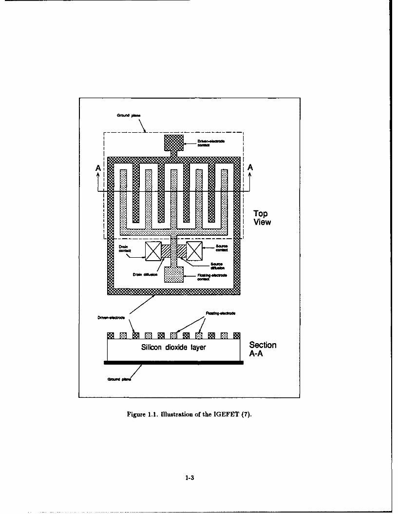
AA
Tio
---- --- oon
Silicon dioxide layer AeciA
Figure 1.1. Illustration of the IGEFET (7).
1-3
Problem Statement
A more comprehensive investigation of the IGEFET's response to changes in the electrical
properties of epoxy resins has been motivated by preliminary research.
Justification. A closer examination of the IGEFET's response to resin cure, with a goal of
locating the characteristic gelation point by analysis of the IGEFET's response data, is warranted.
In his IGEFET research, Wiseman investigated the feasibility of using the IGEFET to monitor a
resin's cure rate (3). He used a well-characterized epoxy resin (Epon 828, Miller-Stephenson
Chemical Co., Danbury, CT), and applied it as a thick film to the IGE structure. Wiseman was
able to show that the IGEFET's response to a thick film of epoxy resin could be attributed to the
changing permittivity of the resin as it cured. Epoxy resins, in general, display a dramatic change
in electrical conductivity when their characteristic gelation point is attained (11:188).
Scope. The purpose of this thesis is to characterize the response of the IGEFET sensor to a
thermosetting epoxy resin system. The cure of this resin has been characterized with respect to
two different isothermal temperature profiles. The data collected was direct current (dc)
resistance of the IGE structure, alternating current (ac) impedance (magnitude and phase) of the
IGE structure, and the transient (time-domain) and spectral (frequency-domain) responses of the
IGEFET to a voltage pulse excitation. The resin was applied directly to the IGE structure, and
the data collected was analyzed to identify its gelation point. Rheological studies of the resins
used in the IGEFET sensor studies were also conducted for the same isothermal temperature
profiles, and the measured viscosity data was used to locate the gelation point of the resin. All
electrical characteristics, measured with respect to time, were compared to the viscosity data,
which were also measured with respect to time. A dramatic change in the electrical
characteristics of the resin was expected to occur as a result of the resin's gelation.
1-4
Definitions. In the interest of improving clarity for this multi-disciplinary research topic,
several fundamental definitions of the key terminology are presented.
An epoxy group, also called an epoxide, is defined as an oxygen atom bound to two carbon
atoms which are also connected in some manner (12:1-1). This term is often used interchangeably
with the term resin.
A resin is a molecule which contains more than one epoxy group (12:1-2). In this thesis, the
terms epoxy resin and resin will be used interchangeably.
The gelation point (or gel point), of a resin can be defined many ways. An abstract,
microscopic definition is that the gelation point corresponds to the moment an infinitely long
polymer chain has been produced (8:272). From a macroscopic and practical perspective, the
gelation point is defined as the moment the resin loses its fluidity, or becomes rubbery. At this
point, bubbles can no longer rise through the material (8:274). A consequence of the differing
definitions for the gelation point is that interpretations of its occurrence in a resin can differ,
given identical sets of data. Therefore, the establishment of a technique for identifying the
gelation point is somewhat arbitrary. The method used in this thesis effort will be to locate the
point at which the storage modulus of the resin (G') is equal to the loss modulus (G") (13:571).
In general, the complex shear modulus (G*) is gi,/en by, G* = G'+ jG", and it is related to
complex viscosity (q") by the expression 17* = G*/w, where w is the angular frequency at which
the material is physically twisted. Additionally, the mechanical loss tangent (tan 6m) is defined to
be the ratio between the loss modulus and the storage modulus (tan 6m =G"/G').
Whenever a dielectric material becomes electrically lossy, its permittivity becomes complex.
The complex permittivity consists of a real part (the relative permittivity, denoted by e), and an
imaginary part (the loss factor, denoted by e") (14:4).
1-5
Approach
The critical milestones implemented in this investigation included a redesign of the IGEFET,
qualification of the revised IGEFET after fabrication, and collection of the resin cure performance
data. These steps are described in the following sections.
IGEF PT Redesign. The previous IGEFET designs contributed by Jenkins and Shin (4, 5)
were largely successful, so the accomplishment of the redesign of the IGEFET was, for the most
part, an exercise of combining the best features from each design.
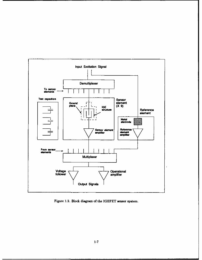
A block diagram of the IGEFET circuit is illustrated in Figure 1.2. The revised integrated
circuit consists of:
1. 3 x 3 matrix of IGEFET sensor elements. Each sensor element is composed of an IGE
structure and a sensor element amplifier.
2. Ground plane. This dielectrically-isolated ground plane, realized from first-level metal,
passes beneath the signal lines an the IGE structures.
3. Demultiplexer. This circuit determines which of the nine sensor elements will be connected
to the input.
4. Multiplexer. This circuit selects the output of one of the sensor element amplifiers.
5. Output interface. Two such interfaces are available at the discretion of the user: first, a
voltage follower, or second, a five-stage operational amplifier which provides additional gain.
6. Reference element. The reference element is composed of a sensor element amplifier
(identical to those fabricated for the IGEFET sensor elements) whose input is tied to a
solid, second-level metal electrode. The area of this electrode is approximately equal to the
combined areas of the driven- and floating-electrodes which compose the IGE structure.
During the collection of IGEFET response data (gain and phase delay, and
frequency-domain response to a voltage pulse excitation), identical sets of data were
1-6
Input Excitation Signal
I DemultiplexerTo sensorerments
Test cepacitors SensorGround F element
_kw _ IGE (X 9) Referenceii element
LL I Metal- -- elmd
ThSensor eement Reerona V
elernentsF
VoltageOperational
Output Signals
Figure 1.2. Block diagram of the IGEFET sensor system.
1-7
collected for the reference element. Comparison of the IGEFET and reference element data
provided information concerning the effect of the experimental conditions on the IGEFET
electronics. In particular, the spectral response of the reference element was subtracted
from the spectral response of the IGEFET to provide the difference Fourier transform
spectrum. The difference Fourier transform spectrum provided information concerning the
spectral response of the IGE structure without the effects of the IGEFET electronics or the
effects of the electrical parasitics in the measurement system.
7. Three parallel-plate test capacitors. These passive elements facilitated characterizing the
field-oxide layer which isolates the ground plane from the IGE structure.
A number of areas have been intentionally exposed on the integrated circuit (IC) die to
facilitate excision of inoperative circuits with an ultrasonic microprobe cutter. In addition, most
important internal nodes are accessible via microprobe bonding pads.
IGEFET Qualification. This milestone was initiated when the IGEFET integrated circuit
packages were received from the Metal-Oxide-Semiconductor Implementation System (MOSIS)
fabrication service. The following steps were accomplished to ensure proper operation of the
IGEFET sensors. A randomly selected sample package was evaluated, and it satisfied the
following criteria:
1. Physical and electrical isolation of the driven- and floating-electrodes was verified by visual
inspection and by requiring a minimum of 30 dB of isolation between them.
2. Proper operation of the multiplexer and demultiplexer was verified. This requirement was
established because each circuit had to provide a minimum isolation of 30 dB relative to
each non-selected signal line.
3. The sensor element amplifier and voltage follower were checked for proper operation relative
to the specified design constraints. Since a previous design was being utilized, the expected
1-8
performance was anticipated to be comparable to the performance realized in that design
effort. As a result, the measured gain at the voltage follower output was approximately 20
dB with a 3-dB cutoff frequency of approximately 450 KHz (4:5-4).
4. The 5-stage operational amplifier was evaluated for proper operation within the specified
design constraints. Only the first stage of the operational amplifier was utilized, and it
yielded an overall gain of approximately 20 dB with a 3-dB cutoff frequency of
approximately 850 KHz.
Faulty components could be bypassed or isolated by trimming the appropriate metal signal
lines with an ultrasonic microprobe cutter and supplementing the remaining circuit with wire
bonds and externally configured electronics.
Performance Data Collection. The resin used in this thesis effort was Epoxy 907
(Miller-Stephenson Co., Danbury, CT), a thermosetting resin with a dielectric filler material. This
resin was selected because of its relatively high viscosity in the uncured state, its low cure
temperature, and its availability. The resin was subjected to electrical and mechanical tests. The
electrical tests, which utilized the IGEFET sensor, are detailed in Table 1.1, and the mechanical
tests are detailed in Table 1.2.
Mechanical Performance Tests. A separate effort was implemented to collect the
mechanical performance data on the resin. The rheological studies were conducted using
instrumentation available at the Materials Division of the Wright Laboratory (WL/MLB). Two
types of tsts were conducted: parallel plate analysis and torsional bar analysis. The purpose of
the parallel plate analysis was to obtain an estimate of the gelation time for the resin, and the
purpose of the torsional bar analysis was to estimate its glass transition temperature.
Electrical Performance Tests. A separate test was conducted for each electrical
characteristic measured (see Table 1.1) to minimize the time interval between data points. For
1-9
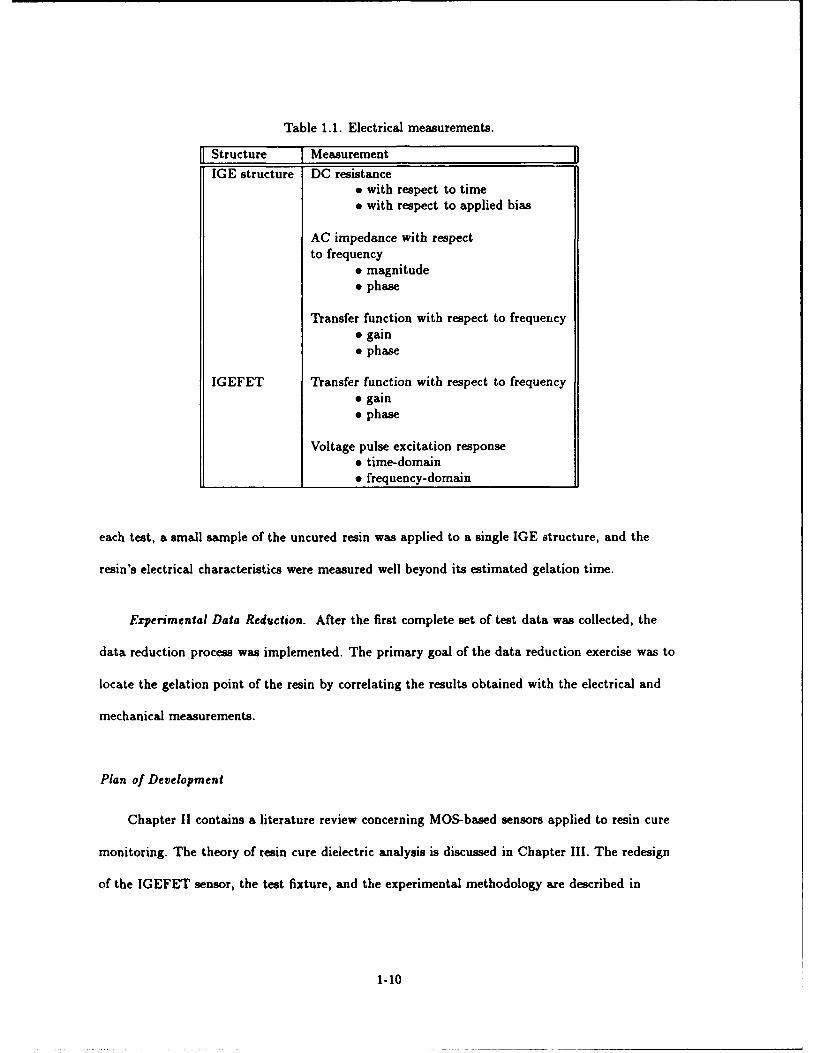
Table 1.1. Electrical measurements.
Structure MeasurementIGE structure DC resistance
" with respect to time" with respect to applied bias
AC impedance with respectto frequency
" magnitude" phase
Transfer function with respect to frequency" gain" phase
IGEFET Transfer function with respect to frequency" gain" phase
Voltage pulse excitation response* time-domain* frequency-domain
each test, a small sample of the uncured resin was applied to a single IGE structure, and the
resin's electrical characteristics were measured well beyond its estimated gelation time.
E'perimentai Data Reduction. After the first complete set of test data was collected, the
data reduction process was implemented. The primary goal of the data reduction exercise was to
locate the gelation point of the resin by correlating the results obtained with the electrical and
mechanical measurements.
Plan of Development
Chapter II contains a literature review concerning MOS-based sensors applied to resin cure
monitoring. The theory of resin cure dielectric analysis is discussed in Chapter III. The redesign
of the IGEFET sensor, the test fixture, and the experimental methodology are described in
1-10
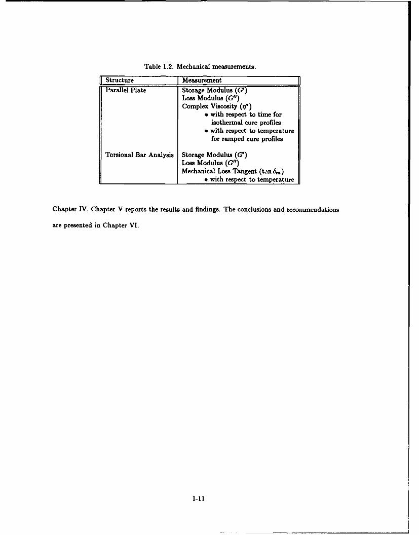
Table 1.2. Mechanical measurements.
Structure Measurement J]Parallel Plate Storage Modulus (G')
Loss Modulus (G")Complex Viscosity (q*)
" with respect to time forisothermal cure profiles
" with respect to temperaturefor ramped cure profiles
Torsional Bar Analysis Storage Modulus (G')Loss Modulus (G")Mechanical Loss Tangent (tai 6m)
* with respect to temperature
Chapter IV. Chapter V reports the results and findings. The conclusions and recommendations
are presented in Chapter VI.
1-11

IL Literature Review of Sensors for In Situ Resin Cure Monitoring
Introduction
The purpose of this literature review is to discuss recent research concerning sensors for in
situ resin cure monitoring. The ability to unobtrusively embed a small sensor in a resin for the
purpose of real-time cure monitoring will facilitate greater control over the cure process and
enhance production of higher quality materials and fabricated parts. This is especially true for
the application of monitoring the cure of advanced composite materials whose mechanical
properties are highly process dependent (2:275).
A number of techniques exist which facilitate the characterization of the resin cure process.
These include Differential Scanning Calorimetry (DSC), Thermal Stimulated Current (TSC),
Relaxation Map Analysis (RMA) spectroscopy, Torsional-Braid Analysis various techniques
which measure electrical impedance characteristics of the resin, and the measurement of optical
characteristics of curing resin systems. However, many of these techniques do not lend themselves
to in situ resin cure monitoring. In this chapter, the development of the techniques and sensors
which facilitate in situ resin cure monitoring is presented.
Fluorescence Sensors
In recent years, a considerable body of research has been performed in the area of
fluorescence monitoring of chemical and viscosity changes that occur during the cure of epoxy
resins. The techniques used by different researchers include the use of dyes which dissolve in the
resin being monitored and the use of dyes which react with epoxide groups, called reactive dye
labelling. The following sections describe the research performed in these areas.
Fluorescence Monitoring with an Internal Standard. Wang and others at the National
Bureau of Standaros have been researching the fluorescence monitoring of resin cure for several
2-1
years. Their technique incorporates a viscosity-insensitive internal standard dye in conjunction
with a dye which is sensitive to changes in local viscosity (15). As the polymerization reaction
proceeds, the fluorescence intensity of the viscosity sensitive dye increases, while the fluorescence
intensity of the viscosity-insensitive dye remains constant. Using a viscosity-insensitive dye
eliminates the reliance upon absolute measures of fluorescence intensities. The researchers
contend that the ability to measure relative intensities is more practical in an industrial setting
(15:455). The results of their research has demonstrated that this technique is capable of
monitoring resin cure throughout the entire cure cycle.
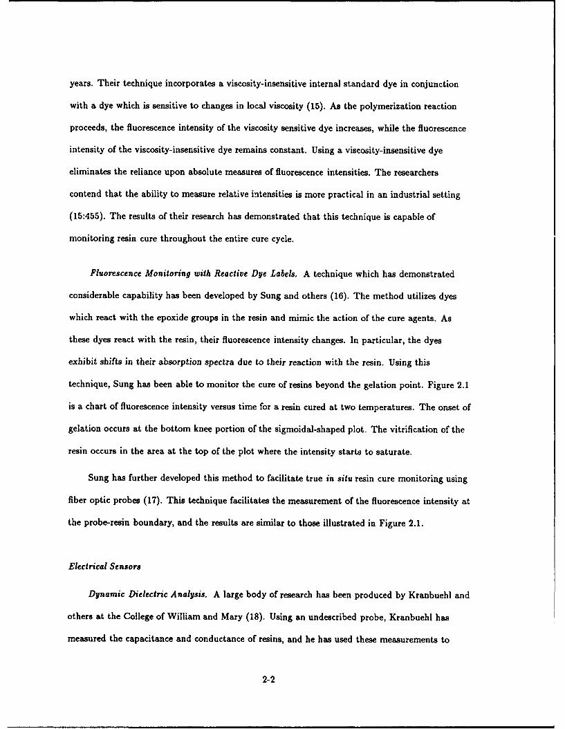
Fluorescence Monitoring with Reactive Dye Labels. A technique which has demonstrated
considerable capability has been developed by Sung and others (16). The method utilizes dyes
which react with the epoxide groups in the resin and mimic the action of the cure agents. As
these dyes react with the resin, their fluorescence intensity changes. In particular, the dyes
exhibit shifts in their absorption spectra due to their reaction with the resin. Using this
technique, Sung has been able to monitor the cure of resins beyond the gelation point. Figure 2.1
is a chart of fluorescence intensity versus time for a resin cured at two temperatures. The onset of
gelation occurs at the bottom knee portion of the sigmoidal-shaped plot. The vitrification of the
resin occurs in the area at the top of the plot where the intensity starts to saturate.
Sung has further developed this method to facilitate true in situ resin cure monitoring using
fiber optic probes (17). This technique facilitates the measurement of the fluorescence intensity at
the probe-resin boundary, and the results are similar to those illustrated in Figure 2.1.
Electrical Sensors
Dynamic Dielectric Analysis. A large body of research has been produced by Kranbuehl and
others at the College of William and Mary (18). Using an undescribed probe, Kranbuehl has
measured the capacitance and conductance of resins, and he has used these measurements to
2-2
If a
600 amK
,'.
400
a0 3
* S I aLog (DirN)
Figure 2.1. Fluorescence intensity (Ij) at 418 nm as a function of cure time for a resin cured attwo different temperatures (16:477).
calculate the relative permittivity and loss factor of the material. The thrust of his research has
been to use these measured and calculated parameters to characterize the extent of the reaction
as a function of time and temperature (18:344). Since the probe design is not unobtrusive, the
samples used in his experiments required considerable preparation.
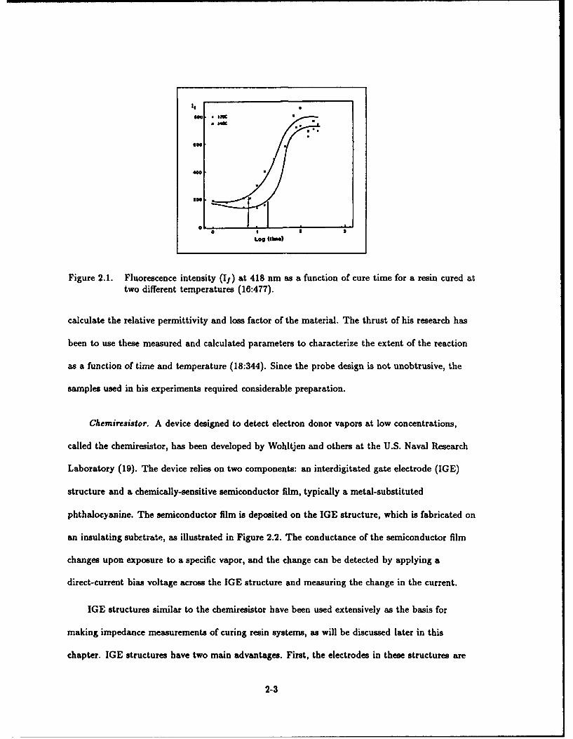
Chemiresistor. A device designed to detect electron donor vapors at low concentrations,
called the chemiresistor, has been developed by Wohltjen and others at the U.S. Naval Research
Laboratory (19). The device relies on two components: an interdigitated gate electrode (IGE)
structure and a chemically-sensitive semiconductor film, typically a metal-substituted
phthalocyanine. The semiconductor film is deposited on the IGE structure, which is fabricated on
an insulating subetrate, as illustrated in Figure 2.2. The conductance of the semiconductor film
changes upon exposure to a specific vapor, and the change can be detected by applying a
direct-current bias voltage across the IGE structure and measuring the change in the current.
IGE structures similar to the chemiresistor have been used extensively as the basis for
making impedance measurements of curing resin systems, as will be discussed later in this
chapter. IGE structures have two main advantages. First, the electrodes in these structures are
2-3
MICROELECTRODE
AI I .. A.
ESTTAAS
Figure 2.2. Diagram of the chemiresistor (19).
fixed. The volumetric shrinkage that most resin systems experience during cure causes the
spacing between electrodes in many other structures (most notably parallel-plate structures) to
change. Changes in electrode spacing make measurements of permittivity and loss factor difficult.
Second, IGE structures are easily fabricated on a microscopic scale using standard integrated
circuit vacuum deposition and photolithographic processes.
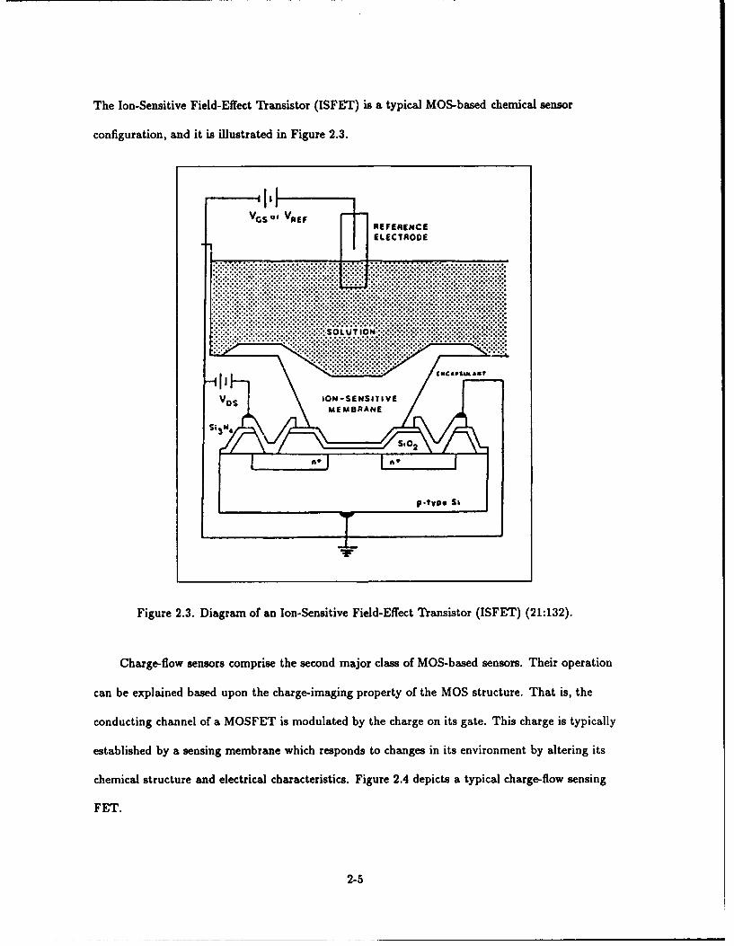
Meial-Oxide-Semiconductor (MOS)-Based Sensors. Sensors incorporating the MOS
structure have been developed to detect a multitude of chemical species and to sense changes in
the electrical properties of materials due to chemical reactions. In general, MOS sensors can be
divided into two major classes: chemical sensors and charge-flow sensors (20:507).
Chemical sensors are those which respond to changes in the chemical potential of the gate
structure of the MOS device. In this class of MOS sensors, the gate material of a typical
MOSFET (which is normally a metal or polysilicon) is replaced by the material to be monitored.
2-4
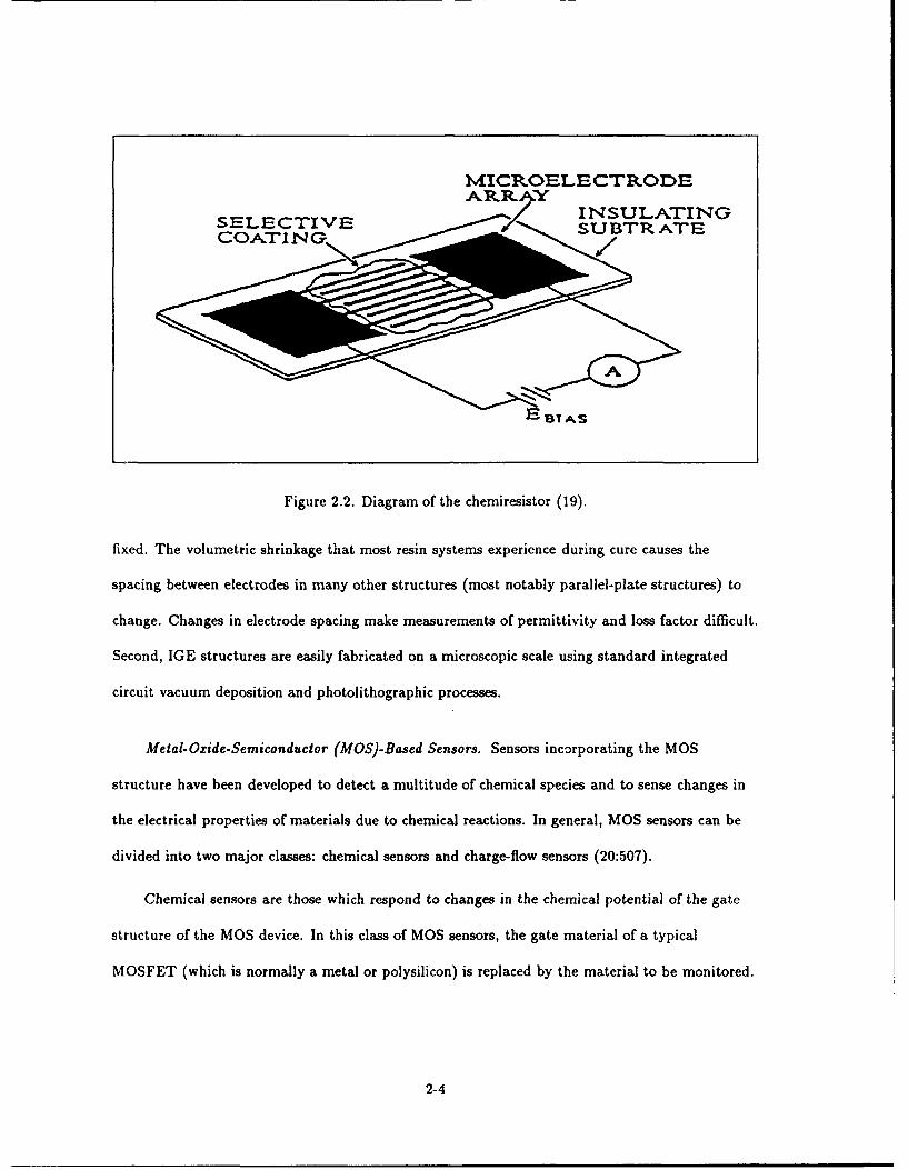
The Ion-Sensitive Field-Effect Transistor (ISFET) is a typical MOS-based chemical sensor
configuration, and it is illustrated in Figure 2.3.
I,VGS oVREF
REFERENCE
ELECTRODE
:':::SOLUSTION
$i 3 4
p type Sa
V
Figure 2.3. Diagram of an Ion-Sensitive Field-Effect Transistor (ISFET) (21:132).
Charge-flow sensors comprise the second major class of MOS-based sensors. Their operation
can be explained based upon the charge-imaging property of the MOS structure. That is, the
conducting channel of a MOSFET is modulated by the charge on its gate. This charge is typically
established by a sensing membrane which responds to changes in its environment by altering its
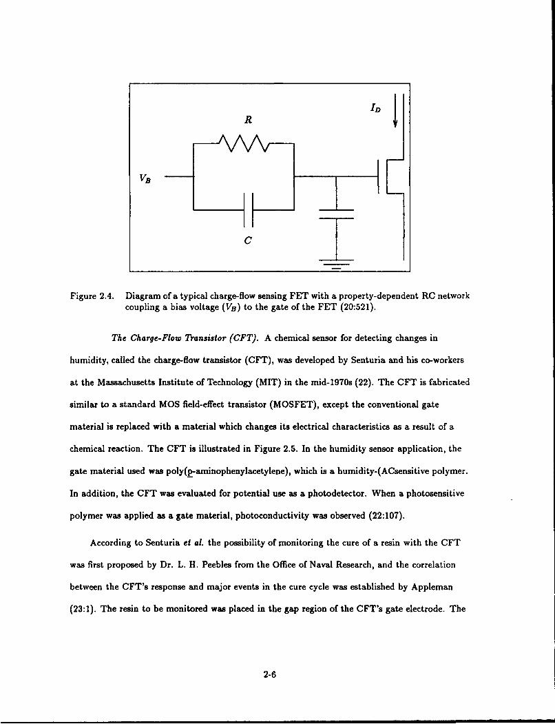
chemical structure and electrical characteristics. Figure 2.4 depicts a typical charge-flow sensing
FET.
2-5
R IDR
V8
C
Figure 2.4. Diagram of a typical charge-flow sensing FET with a property-dependent RC networkcoupling a bias voltage (VB) to the gate of the FET (20:521).
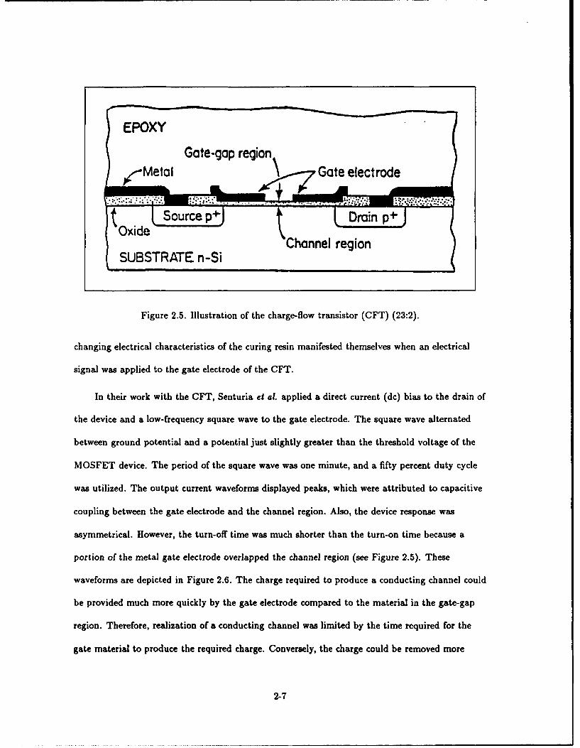
The Charge-Flow Transistor (CFT). A chemical sensor for detecting changes in
humidity, called the charge-flow transistor (CFT), was developed by Senturia and his co-workers
at the Massachusetts Institute of Technology (MIT) in the mid-1970s (22). The CFT is fabricated
similar to a standard MOS field-effect transistor (MOSFET), except the conventional gate
material is replaced with a material which changes its electrical characteristics as a result of a
chemical reaction. The CFT is illustrated in Figure 2.5. In the humidity sensor application, the
gate material used was poly(p-aminophenylacetylene), which is a humidity-(ACsensitive polymer.
In addition, the CFT was evaluated for potential use as a photodetector. When a photosensitive
polymer was applied as a gate material, photoconductivity was observed (22:107).
According to Senturia et al. the possibility of monitoring the cure of a resin with the CFT
was first proposed by Dr. L. H. Peebles from the Office of Naval Research, and the correlation
between the CFT's response and major events in the cure cycle was established by Appleman
(23:1). The resin to be monitored was placed in the gap region of the CFT's gate electrode. The
2-6
changing elcrclc ara teicao th uresinm ifseth sleswnanlcrcl
si naMelwaG applied to theig G ate electrode
norw e t ed drain ofOxide~Channel region
SUBSTRATE n-Si
Figure 2.5. Illustration of the charge-flow transistor (OFT) (23:2).
changing electrical characteristics of the curing resin manifested themselves when an electrical
signal was applied to the gate electrode of the CFT.
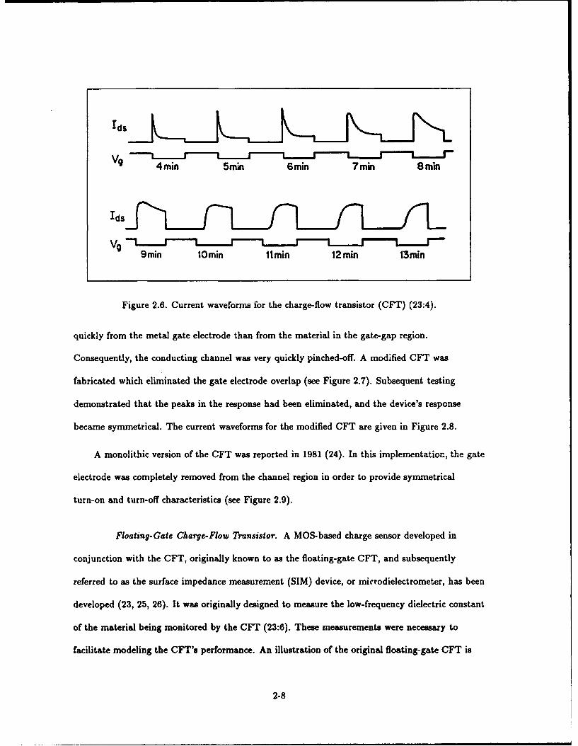
In their work with the CFT, Senturia et aL. applied a direct current (dc) bias to the drain of
the device and a low-frequency square wave to the gate electrode. The square wave alternated
between ground potential and a potential just slightly greater than the threshold voltage of the
MOSFET device. The period of the square wave was one minute, and a fifty percent duty cycle
was utilized. The output current waveforms displayed peaks, which were attributed to capacitive
coupling between the gate electrode and the channel region. Also, the device response was
asymmetrical. However, the turn-off time was much shorter than the turn-on time because a
portion of the metal gate electrode overlapped the channel region (see Figure 2.5). These
waveforms are depicted in Figure 2.6. The charge required to produce a conducting channel could
be provided much more quickly by the gate electrode compared to the material in the gate-gap
region. Therefore, realization of a conducting channel was limited by the time required for the
gate material to produce the required charge. Conversely, the charge could be removed more
2-7
V9 4in 5min 6min 7min 8an
g 9min 10min 11min 12 min 13min
Figure 2.6. Current waveforms for the charge-flow transistor (CFT) (23:4).
quickly from the metal gate electrode than from the material in the gate-gap region.
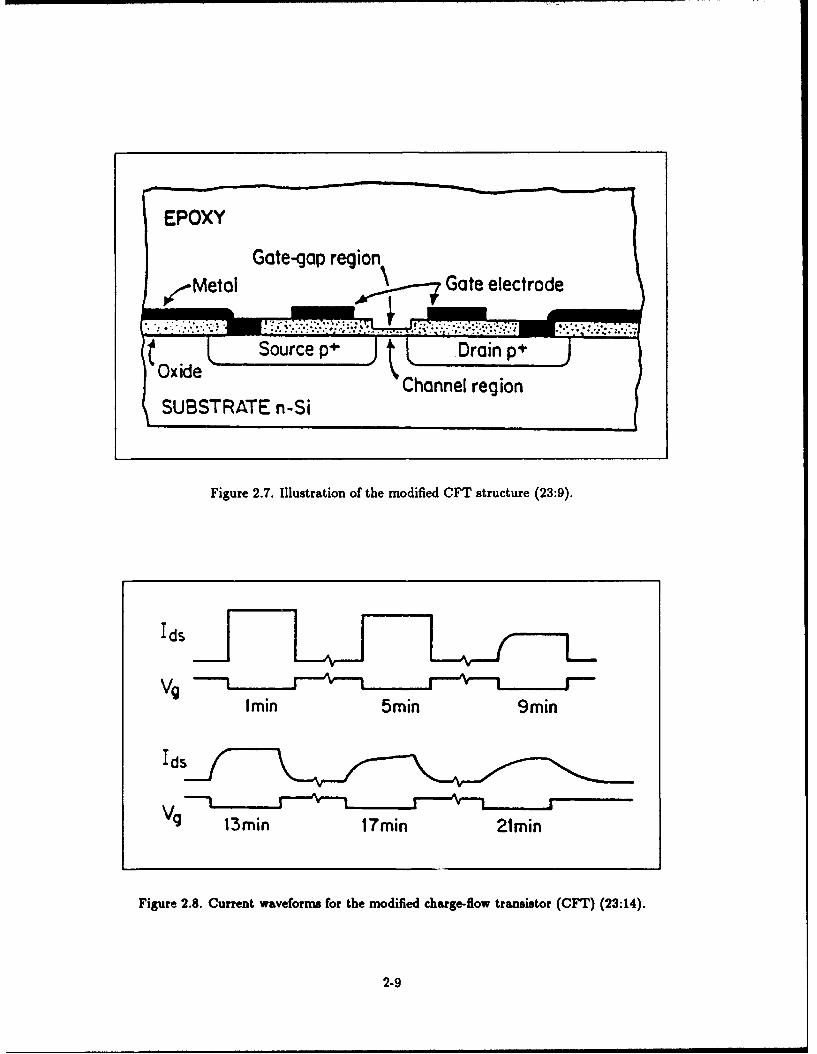
Consequently, the conducting channel was very quickly pinched-off. A modified CFT was
fabricated which eliminated the gate electrode overlap (see Figure 2.7). Subsequent testing
demonstrated that the peaks in the response had been eliminated, and the device's response
became symmetrical. The current waveforms for the modified CFT are given in Figure 2.8.
A monolithic version of the CFT was reported in 1981 (24). In this implementation, the gate
electrode was completely removed from the channel region in order to provide symmetrical
turn-on and turn-off characteristics (see Figure 2.9).
Floating-Gate Charge-Flow Transistor. A MOS-based charge sensor developed in
conjunction with the CFT, originally known to as the floating-gate CFT, and subsequently
referred to as the surface impedance measurement (SIM) device, or microdielectrometer, has been
developed (23, 25, 26). It was originally designed to measure the low-frequency dielectric constant
of the material being monitored by the CFT (23:6). These measurements were necessary to
facilitate modeling the CFT's performance. An illustration of the original floating-gate CFT is
2-8
EPOX
FEEOY Gate-gap region
,,..Metal Gate electrode
id Source p4, Drain p+
Channel regionSUBSTRATE n-Si
Figure 2.7. Illustration of the modified CFT structure (23:9).
Ids
Vg mi 5min 9min
V9 13ain 17min 21min
Figure 2.8. Current waveforms for the modified charge-flow transistor (OFT) (23:14).
2-9
SourceDri
electrode
Figure 2.9. The CFT structure utilized in the monolithic circuit (24:66).
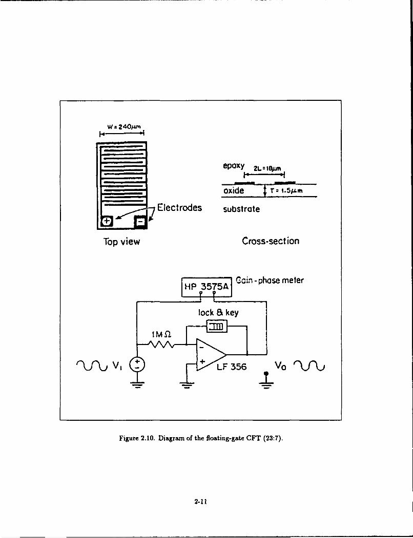
presented in Figure 2.10. The interdigitated electrode structure (IGE) illustrated in Figure 2.10
was utilized in the feedback loop of an operational amplifier. The structure was coated with the
material to be monitored, and an alternating current signal was used as the excitation source.
The conductance and capacitance were measured, and these values were used to calculate the
relative permittivity, loss factor, and loss tangent. Experiments conducted to evaluate the
device's performance as a resin cure monitor revealed that a sharp decrease in the calculated
relative permittivity and loss factor of the resin being monitored occurred at the resin's gelation
point (23:16).
The original CFT design had several disadvantages. It was difficult to calibrate, and the
sensor's output signal was nonlinear. In contrast, the floating-gate CFT could be accurately
calibrated and linear device models could be used to analyze the output signal (26). Most of the
continuing research at MIT concerning resin cure monitoring has utilized the floating-gate CFT,
and in 1983, a commercial version of the device became available (27).
Interdigitated Gate Electrode Field-Effect Transistor (IGEFET). A device similar to
the CFT is the chemically-sensitive field-effect transistor (CHEMFET), developed by Janata and
his co-workers at the University of Utah (28). The goal of their research was to develop a
2-10
Wz=24OW
epoxy 2L=8"
oxide r 1.5km
ii- Electrodes substrate
Top view Cross-section
HP 355A P se meter
lock Ek key
l~I-
Figure 2.10. Diagram of the floating-gate CFT (23:7).
2-11
MOS-based chemical sensor for the detection of organophosphorus compounds and pesticides.
Four types of CHEMFETs were evaluated: enzyme-coupled, galvanostatic, catalytic, and work
function. The criteria for selecting an optimum configuration included: a concentration sensitivity
of 1-10 parts-per-billion, a response time of less than ten seconds, complete reversibility in thirty
seconds, a shelf life of six months, and an operational life of ten days of continuous use (28:666).
Based on these criteria, the work function CHEMFET configuration was chosen.
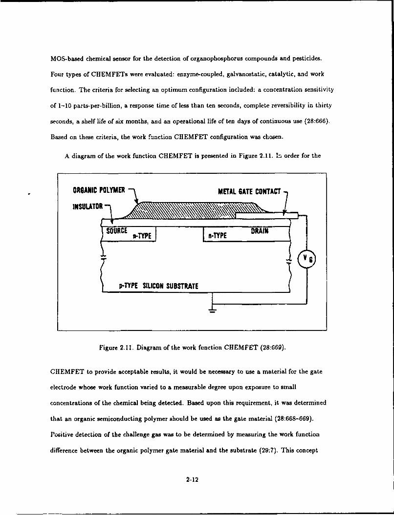
A diagram of the work function CHEMFET is presented in Figure 2.11. In order for the
ORGANIC POLYMER METAL GATE CONTACT
INSULATOR
sou~c1 VCi
Figure 2.11. Diagram of the work function CHEMFET (28:669).
CHEMFET to provide acceptable results, it would be necessary to use a material for the gate
electrode whose work function varied to a measurable degree upon exposure to small
concentrations of the chemical being detected. Based upon this requirement, it was determined
that an organic semiconducting polymer should be used as the gate material (28:668-669).
Positive detection of the challenge gas was to be determined by measuring the work function
difference between the organic polymer gate material and the substrate (29:7). This concept
2-12
required that the resistive effects of the gate electrode contacts be negligible; that is, ohmic
gate-to-polymer contacts were needed. However, ohmic contacts to organic materials are difficult
to realize. Experiments to determine an optimum contact material revealed that the observed
change in the dc resistance of the CHEMFET was primarily due to the change of the contact
resistance upon exposure to the challenge gas. Since changes in the contact resistance could not
be separated from changes in the work function difference between the gate material and the
substrate, it was determined that the CHEMFET work function difference configuration would
not function for the detection of organophosphorus compounds.
As a result of this apparent setback, Janata and Gehmlich decided that impedance
measurements should be studied as an alternative approach (29:8). Gehmlich designed an
interdigitated copper electrode structure on a printed circuit board that was similar to the
floating-gate CFT. The interdigitated electrode structure was coated with a film of polymeric
material known to be sensitive to organophosphorus compounds. Tests performed with this device
revealed improved sensitivity (at low frequencies) to varying concentrations of organophosphorus
compounds (29:11).
An improved version of the fundamental interdigitated electrode structure is realized with
the interdigitated gate electrode field-effect transistor (IGEFET). The IGEFET is essentially a
MOSFET with an interdigitated gate electrode structure, as illustrated in Figure 2.12. Thesis
research by Wiseman, Jenkins, and Shin has shown the IGEFET to be sensitive to very small
concentrations of organophosphorus compounds and nitrogen dioxide when thin films of
metal-doped phthalocyanines were deposited on the IGE structure (3, 4, 5).
Preliminary research by Wiseman indicates that the IGEFET may be useful as a resin cure
monitoring sensor (3:6-4). Of particular interest was the spectral response of the IGEFET to a
pulsed voltage excitation signal. The greatest degree of change in the spectral response occurred
with the low frequency harmonics of the input signal, which was a voltage pulse.
2-13
Ground Plane
AA
Vie
Gsource
Figure2.12.Diagrm of he IGFET 7)
so-14
Summary
Se cral sensors and techniques have been investigated for monitoring the cure of epoxy
resins. In particular, two basic classes of sensors were described: fluorescence intensity monitors
and electrical impedance monitors.
Fluorescence monitors show great promise, but the use of a fiber-optic cable to realize a
compact sensor configuration using this technique is still under development.
Two broad categories of electrical impedance resin cure monitoring techniques were
discussed: dynamic dielectric analysis and MOS-based sensors. Dynamic dielectric analysis is
primarily used to characterize the cure of resins, and it could be used in quality control processes.
The probe described is not unobtrusive. One MOS-based chemical sensor for monitoring resin
cure is the charge-flow transistor (CFT), but the CFT technC gy has not been rigorously pursued
due to the device's nonlinear response and difficulties encountered in its calibration. Another
MOS-based charge sensor developed at the same time as the CFT is the floating-gate CFT, or
microdielectrometer. It has proven effective as a device for monitoring resin cure, but it possesses
limitations which restrict its practical utility. Another charge sensor for monitoring resin cure is
the interdigitated gate electrode field-effect transistor (IGEFET), which is an evolutionary
extension of research concerned with the work function chemically-sensitive field-effect transistor
(CHEMFET).
2-15

III. Theory of IGEFET Resin Cure Monitoring
Introduction
The research in this thesis involved the measurement of the electrical and mechanical
(physical) characteristics of a curing resin system. To explain the measurements requires an
understanding of the underlying physical processes manifested when a resin cures. To this end,
this chapter includes a discussion of the electrical processes at work in a curing resin, and an
overview of the dynamic physical mechanisms involved.
Polarization Mechanisms in Dielectric Materials
In the presence of an electric field, the response of a dielectric material is manifested through
a mechanism called polarization. That is, the electric dipoles in the material tend to align
themselves parallel to the direction of an externally applied electric field. Assuming that the
dielectric is isotropic, a vector, P, known as the polarization, can be assigned to the material,
where each incremental volume, dV, has associated with it, an incremental dipole moment, Pi.
Integrating the quantity PjdV over the volume of the material contained between the electrodes
used to apply the electric field yields the polarization, P, which describes the magnitude and
direction of the net dipole moment per unit volume.
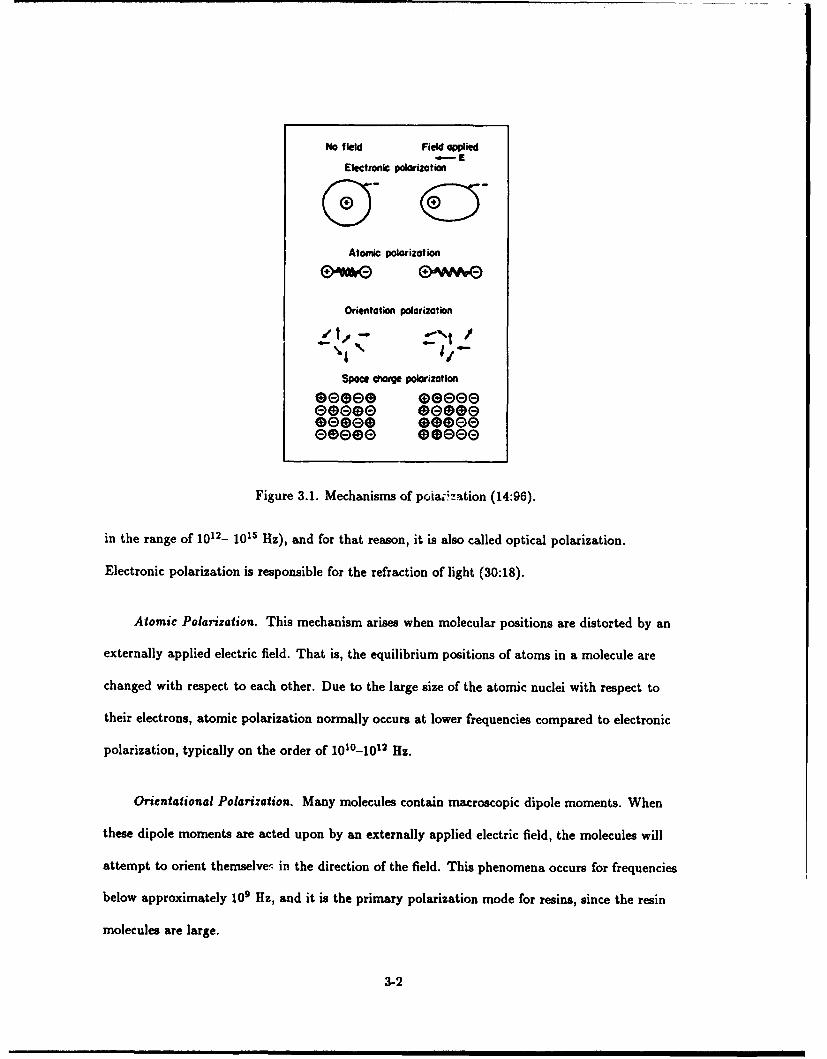
The mechanisms which contribute to polarization include electronic polarization, atomic
polarization, orientational polarization, and interfacial polarization (30:18). A schematic
representation of the polarization mechanisms is presented in Figure 3.1. These mechanisms will
now be discussed.
Electronic Polarization. This type of polarization is caused by a displacement of the
electrons of an atom with respect to its nucleus. This usually occurs at high frequencies (typically
3-1
No field Field applied
Electronic polarization
Atomic polarization
Orientation polarization
Space &rW polarization
Geoee oeeeeeoeee eeoeeee eeeeDeeee 09eee
Figure 3.1. Mechanisms of poiaz-vation (14:96).
in the range of 1012- 1015 Hz), and for that reason, it is also called optical polarization.
Electronic polarization is responsible for the refraction of light (30:18).
Atomic Polarization. This mechanism arises when molecular positions are distorted by an
externally applied electric field. That is, the equilibrium positions of atoms in a molecule are
changed with respect to each other. Due to the large size of the atomic nuclei with respect to
their electrons, atomic polarization normally occurs at lower frequencies compared to electronic
polarization, typically on the order of 1010-1012 Hz.
Orientational Polarization. Many molecules contain macroscopic dipole moments. When
these dipole moments are acted upon by an externally applied electric field, the molecules will
attempt to orient themselves in the direction of the field. This phenomena occurs for frequencies
below approximately 109 Hz, and it is the primary polarization mode for resins, since the resin
molecules are large.
3-2
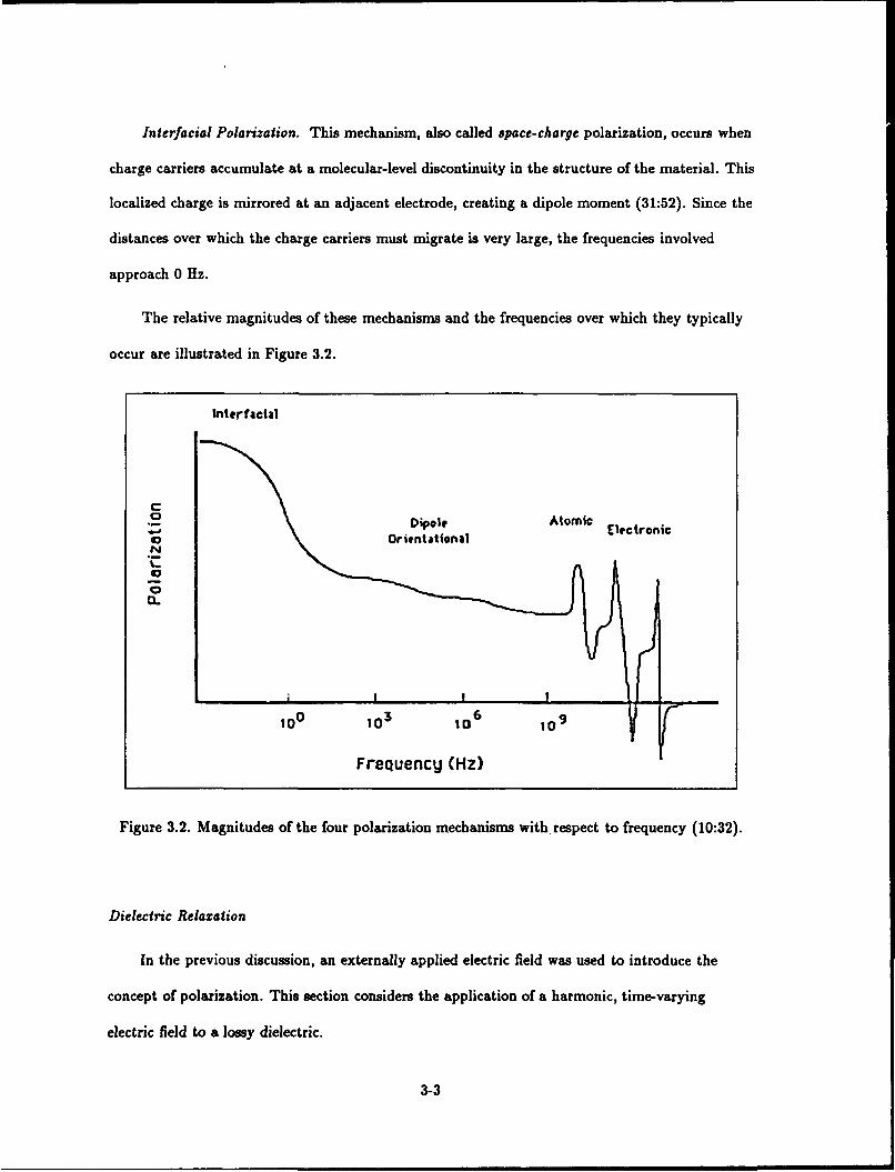
Interfacial Polarization. This mechanism, also called space-charge polarization, occurs when
charge carriers accumulate at a molecular-level discontinuity in the structure of the material. This
localized charge is mirrored at an adjacent electrode, creating a dipole moment (31:52). Since the
distances over which the charge carriers must migrate is very large, the frequencies involved
approach 0 Hz.
The relative magnitudes of these mechanisms and the frequencies over which they typically
occur are illustrated in Figure 3.2.
Interfacl
C<0 Dipole AtomicOa Electronic
40 OrientationalN
00
io i o i
100 103 10o6 19
Frequency (Hz)
Figure 3.2. Magnitudes of the four polarization mechanisms with, respect to frequency (10:32).
Dielectric Relaxation
In the previous discussion, an externally applied electric field was used to introduce the
concept of polarization. This section considers the application of a harmonic, time-varying
electric field to a lossy dielectric.
3-3
Complez Permittivity. An externally applied, harmonically-varying electric field acting on a
dielectric may be described as:
E = E0 coswt (3.1)
where E is the vector representing the applied electric field, Eo is the amplitude of the applied
electric field, w is its radian frequency, and t is time. If the dielectric is ideal, that is, if it is a
lossless material, the current flow through the material will only be displacement current. In this
case, the permittivity associated with the material is a pure real number. If, however, the
material is lossy (non-ideal), a complex permittivity results. Demonstration of this concept car.
be supported by applying basic electromagnetic theory. That is, the time-varying electric field has
associated with it, a time-varying magnetic field, H. The total current density, JT, induced by
this magnetic field is given by Maxwell's representation of Ampere's Law in point form:
V x H =- (3.2)
For an ideal dielectric, JT can be expressed as:
O DJT = O- (3.3)
where JT becomes the displacement current density in the dielectric, and D is the electric flux
density. In a more general sense, though, some loss will be experienced in the form of conduction
current density, JC, and Equation 3.3 becomes:
8DJT = Jc + -- (3.4)
3-4
Substituting the previous relationship into Equation 3.2 yields:
ODV x H = Jc + --. (3.5)
In phasor notation (harmonic field variations), this can be rewritten as:
V x H = Jc +jwD (3.6)
where j represents the unit imaginary number, given by, j = VFT.
The electric flux density is given by:
D = c£coE (3.7)
where c' is the relative permittivity of the material, and co is the permittivity of free space.
Substituting this relationship into Equation 3.6 gives:
V x H = Jc + jwc'cOE. (3.8)
Ampere's Law in point form states that Jc = aE, where a is the electrical conductivity of the
dielectric. Substituting this expression into Equation 3.8 yields:
V x H = aE + c'coE. (3.9)
Rearranging Equation 3.9 gives:
VxH=jwcoE t - J . (3.10)
3-5
Coubistent with the prior discussion, the quantity o/wo is related to the material's dielectric loss.
Therefore, the loss factor of the material is defined as, e' = /weo. Equation 3.10 then becomes:
V x H = jwcoE(e' - je"). (3.11)
The complex relative permittivity, c*, is then defined by:
C* = C, - ". (3.12)
A related figure of merit, the loss tangent, is given as:
tan6 = -- (3.13)
where 6. is the phase angle associated with the total current density vector, JT. The sub-script
"e" is used to prevent confusion between the loss tangent associated with the total current
density, and the mechanical loss tangent, which will be described later in this chapter.
Debhe Equations. If a static electric field is applied to a dielectric and the material is
allowed to respond via the polarization mechanisms discussed earlier in this chapter, and then the
field is instantaneously removed, the polarization decays towards its equilibrium value according
to a decay factor, a(t), which was described by Debye as (32:84):
a(t) = a(O)e - '/ (3.14)
where a(0) is the value of a(t) at t = 0 (due to molecular dipole orientation), and r is the
characteristic relaxation time of the material. The characteristic relaxation time (r) may depend
upon temperature, but not on time (31:68).
3-6
If a time-varying field is applied to the dielectric, the material will change to achieve
maximum polarization, but if the frequency is too high, the material will not have sufficient time
to attain its maximum value. Consequently, the permittivity of the material is said to be relaxed.
Thus, the permittivity of the material is a frequency-dependent quantity, and this dependence is
demonstrated by the equation (31:67):
C'(W) = C". + j a(t)e-I'dt (3.15)
where co is a constant equal to the value of the permittivity at infinite frequency. Physically, c,,
corresponds to the permittivity value which is attained instantaneously when the external electric
field is applied. This quantity is also called the optical dielectric constant, because it can be
described by the optical (electronic) polarization mechanism (14:175).
Substituting the exponential description of the decay factor into Equation 3.15 yields:
C'(W) = c" + a(O)e-'¢Y widt. (3.16)
Integrating this expression gives:
w0+ a(O) (3.17)
The static permittivity of the material, c,, can be determined by setting w = 0 in Equation 3.17.
That is,
is = coo -+ rc(0). (3.18)
Rearranging Equation 3.18 yields the value of a(0):
C' - coo
a(O) = (3.19)
3-7
Substituting this result into Equation 3.14, yields:
o(t) = - COO-t/. (3.20)T
Similarly, substituting Equation 3.20 into Equation 3.16 again gives:
C*(w) = o + 00 -, e_'/reJwtdt (3.21)
= - exp ]dt (3.22)
E*(W) = coo+ - . (3.23)
For an ideal dielectric (lossless), this last equation is valid for describing the material's
relative permittivity. However, for a lossy dielectric, the complex relative permittivity is,
* = €'- )e". Therefore, equating the real and imaginary components of the last two expressions
yields:
= ' -coo (3.24)
and
(C. - Cw)Wr (3.25)1+W2 r2
The loss tangent is given by:
tan6, =-- (3.26)
or
tan 6. = ( -. OO )W " (3.27)C, + CooW
2 T 2 (
The equations for c', c", and tan 6, are called the Debye equations (31:68). For dielectrics with a
single characteristic relaxation time, these relationships are valid. The behavior of t -tnd c" are
plotted in Figure 3.3. A plot of c' versus c" is illustrated in Figure 3.4. The values of c' and e" are
3-8
C
0
log
E
Figure
3.3. Real
and imaginary
components
of the complex
relative
p(,-mittivity
of a dielectric
as a function
of frequency
(33:34).
Figure
3.4. Plot
of
e
versus
e'
for a syst
m with
a single relaxation
time (w
increases
from a
value of zero
ate=
c,
and increases
in a counter-clockwise
direction)
(30:44).
3-9
measured as a function of frequency. The point corresponding to w = 0 is c.. Since c.. can not be
measured directly, the curve is usually extrapolated, and the value is determined graphically
(numerically). The resultant plot in Figure 3.4 is called a Debye semicircle, and it is useful to
determine if a system has only one characteristic relaxation time.
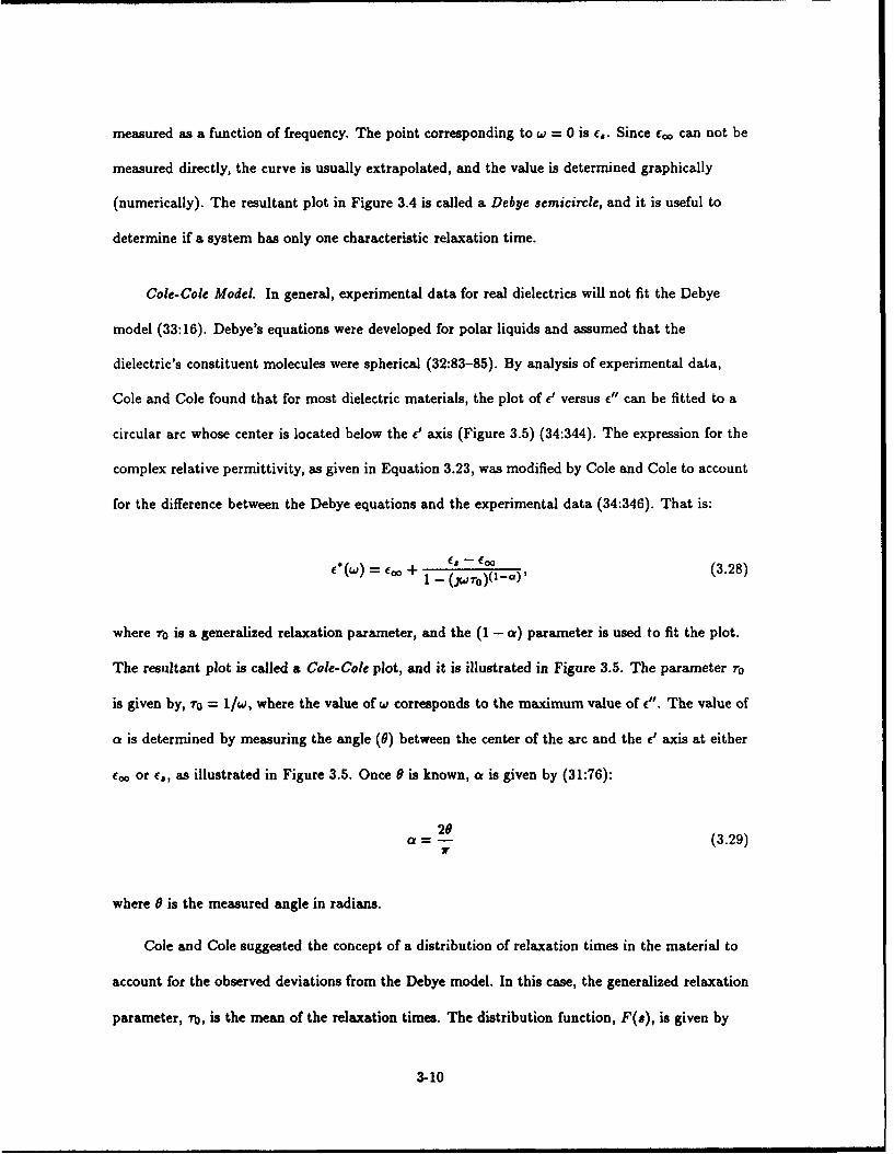
Cole-Cole Model. In general, experimental data for real dielectrics will not fit the Debye
model (33:16). Debye's equations were developed for polar liquids and assumed that the
dielectric's constituent molecules were spherical (32:83-85). By analysis of experimental data,
Cole and Cole found that for most dielectric materials, the plot of c' versus c" can be fitted to a
circular arc whose center is located below the c' axis (Figure 3.5) (34:344). The expression for the
complex relative permittivity, as given in Equation 3.23, was modified by Cole and Cole to account
for the difference between the Debye equations and the experimental data (34:346). That is:
-= (3.28)1 -
where 7-0 is a generalized relaxation parameter, and the (1 - a) parameter is used to fit the plot.
The resultant plot is called a Cole-Cole plot, and it is illustrated in Figure 3.5. The parameter ro
is given by, ro = 1/w, where the value of w corresponds to the maximum value of c". The value of
a is determined by measuring the angle (0) between the center of the arc and the c' axis at either
coo or c,, as illustrated in Figure 3.5. Once 0 is known, a is given by (31:76):
= 20 (3.29)
where 0 is the measured angle in radians.
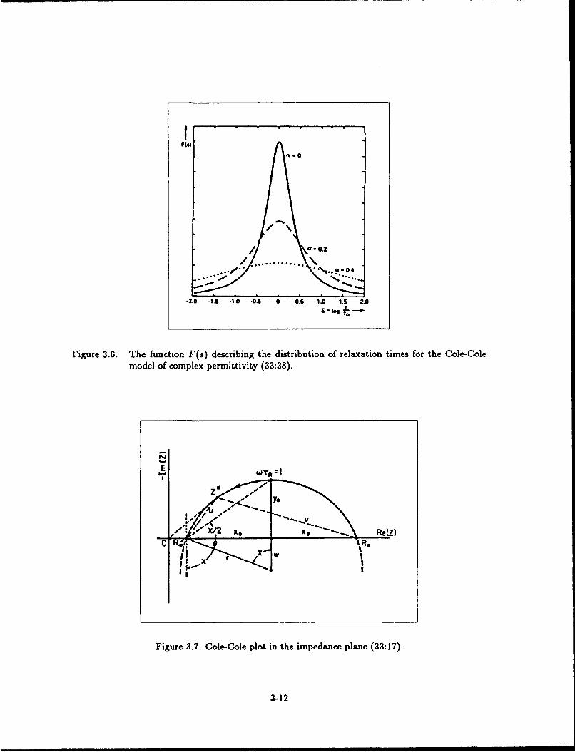
Cole and Cole suggested the concept of a distribution of relaxation times in the material to
account for the observed deviations from the Debye model. In this case, the generalized relaxation
parameter, r0 , is the mean of the relaxation times. The distribution function, F(s), is given by
3-10
8S
Figure 3.5. Cole-Cole plot of a dielectric (31:76).
(34:350):
1 sin ao3.2z cosh(1 - a)s - cos ar (3.30)
where s = ln(r/r). This distribution is plotted in Figure 3.6 for different values of a. Cole and
Cole mention that, while Equation 3.30 is an exact representation of the circular arc, it is difficult
to satisfactorily account for such a distribution (34:350-351).
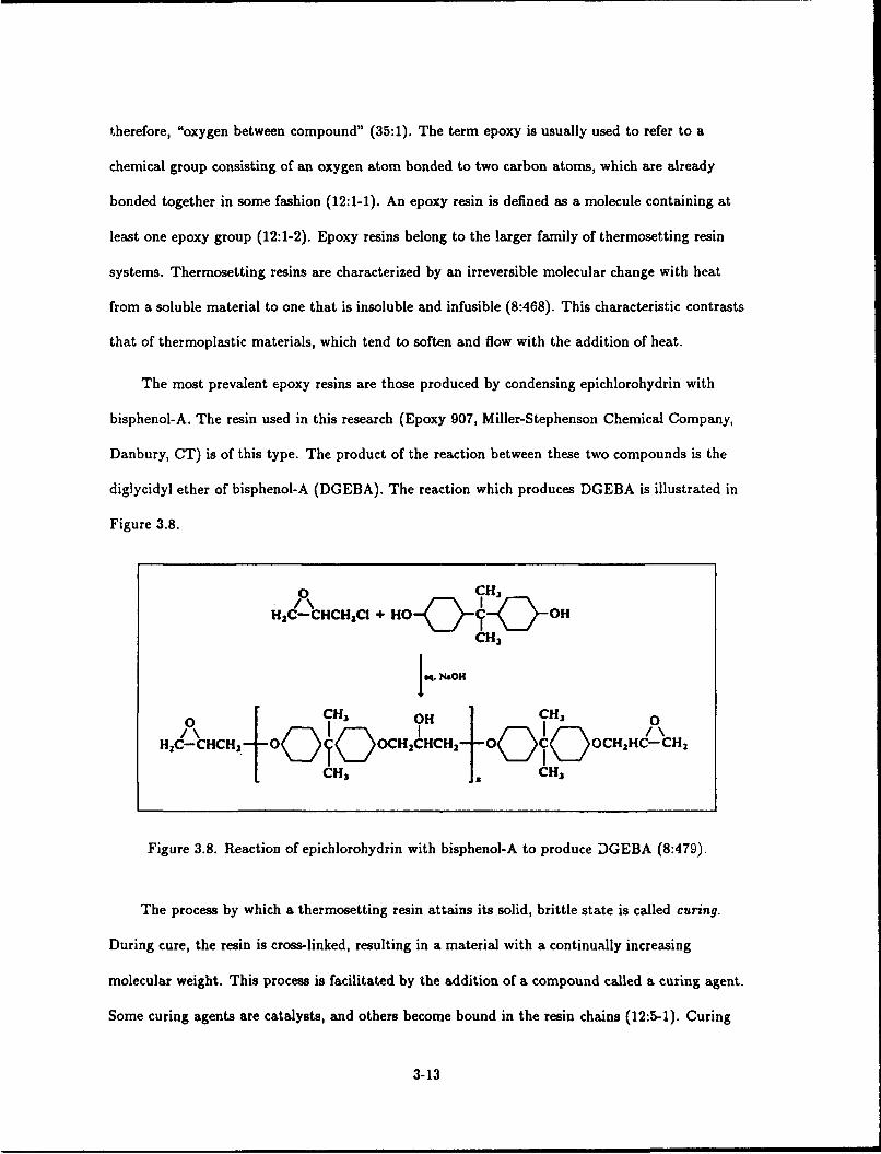
The representations of the relationship between the relative permittivity, loss factor, and
frequency are useful when attempting to characterize the nature of the relaxation time, or
distribution of relaxation times, of a dielectric material. While it is difficult to measure the
relative permittivity and loss factor directly, this information is embedded in the impedance of
the material. A plot of the real part of the impedance versus the imaginary part of the impedance
in given in Figure 3.7.
Epoxy Resin Systems
The term epoxy is actually a corruption of the word epozide. The base of the word is oxygen,
and the prefix is derived from the Greek, and means over or between. The meaning of the word is,
3-11
t ........F~0.4
-2.o -1.5 -. 0 -0.5 0 0.5 1.0 1.5 2.0
Figure 3.6. The function F(s) describing the distribution of relaxation times for the Cole-Colemodel of complex permittivity (33:38).
Nz
II I
Figure 3.7. Cole-Cole plot in the impedance plane (33:17).
3-12
therefore, "oxygen between compound" (35:1). The term epoxy is usually used to refer to a
chemical group consisting of an oxygen atom bonded to two carbon atoms, which are already
bonded together in some fashion (12:1-1). An epoxy resin is defined as a molecule containing at
least one epoxy group (12:1-2). Epoxy resins belong to the larger family of thermosetting resin
systems. Thermosetting resins are characterized by an irreversible molecular change with heat
from a soluble material to one that is insoluble and infusible (8:468). This characteristic contrasts
that of thermoplastic materials, which tend to soften and flow with the addition of heat.
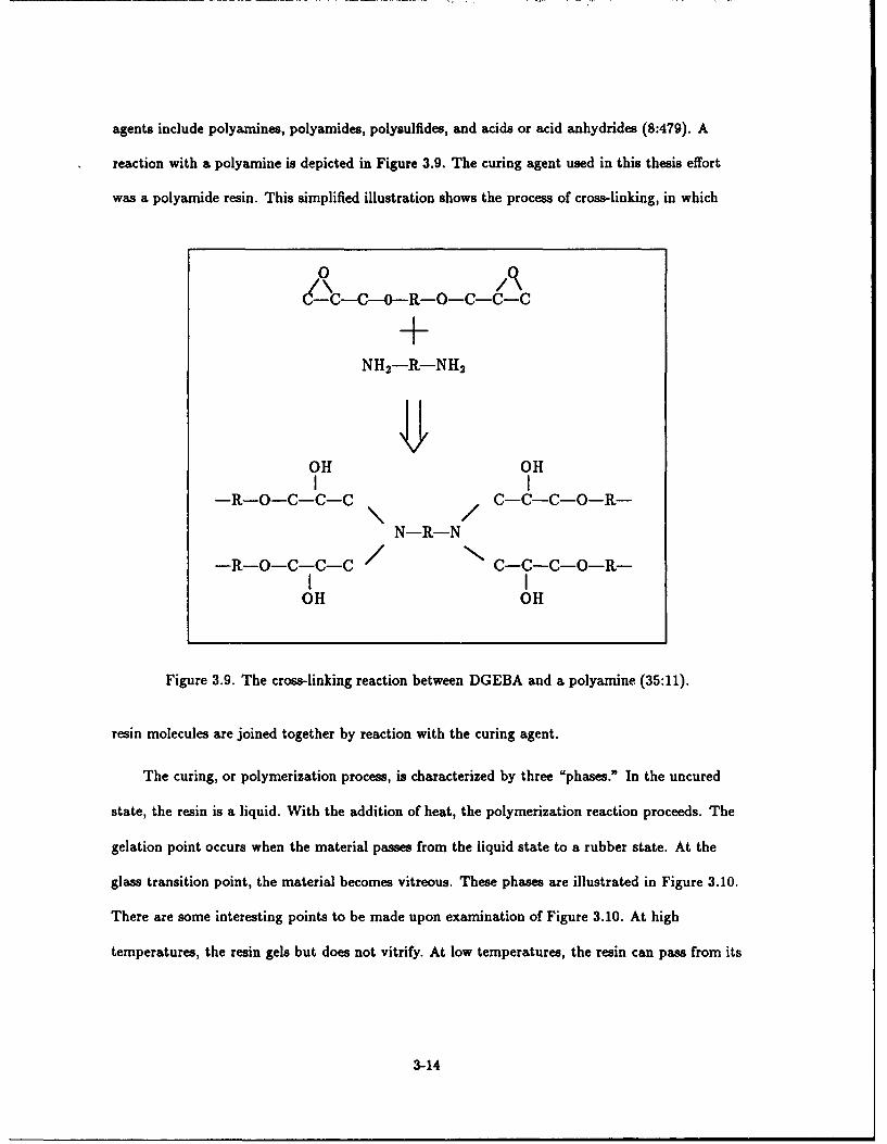
The most prevalent epoxy resins are those produced by condensing epichlorohydrin with
bisphenol-A. The resin used in this research (Epoxy 907, Miller-Stephenson Chemical Company,
Danbury, CT) is of this type. The product of the reaction between these two compounds is the
diglycidyl ether of bisphenol-A (DGEBA). The reaction which produces DGEBA is illustrated in
Figure 3.8.
H2C-CHCH2 CI + HO
CH3
I N&OH
o0 ICH, OH 1cH, 0HI - -0OCH2 IHCH2 4 -OC-j,(J
H~CCHH1 CH3 CH3
Figure 3.8. Reaction of epichlorohydrin with bisphenol-A to produce DGEBA (8:479).
The process by which a thermosetting resin attains its solid, brittle state is called curing.
During cure, the resin is cross-linked, resulting in a material with a continually increasing
molecular weight. This process is facilitated by the addition of a compound called a curing agent.
Some curing agents are catalysts, and others become bound in the resin chains (12:5-1). Curing
3-13
agents include polyamines, polyamides, polysulfides, and acids or acid anhydrides (8:479). A
reaction with a polyamine is depicted in Figure 3.9. The curing agent used in this thesis effort
was a polyamide resin. This simplified illustration shows the process of cross-linking, in which
o 0d-C-C--O--R-O-C-C-C
±NH 2 -R-NH2
OH OHI I-R--O-C-C-C C-C-C-O-R--\ /
N-R-N-R-o-C-C-C /c-c-c-o-R-
I IOH OH
Figure 3.9. The cross-linking reaction between DGEBA and a polyamine (35:11).
resin molecules are joined together by reaction with the curing agent.
The curing, or polymerization process, is characterized by three "phases." In the uncured
state, the resin is a liquid. With the addition of heat, the polymerization reaction proceeds. The
gelation point occurs when the material passes from the liquid state to a rubber state. At the
glass transition point, the material becomes vitreous. These phases are illustrated in Figure 3.10.
There are some interesting points to be made upon examination of Figure 3.10. At high
temperatures, the resin gels but does not vitrify. At low temperatures, the resin can pass from its
3-14
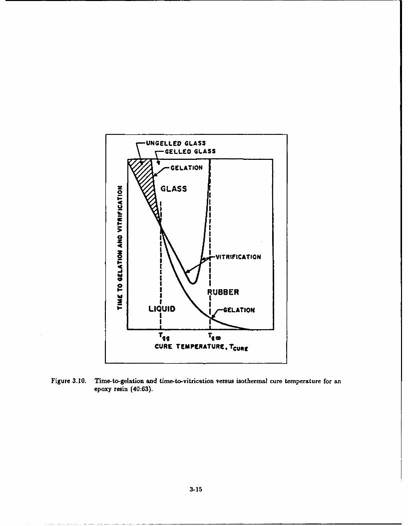
UNGELLED GLASS
7GELLEO GLASS
0
4
za VITRIFICATIONP.-
RUBE-5
I- LIQUID GELATION
T21TCURE T EM PERATUREj TCURC
Figure 3.10. Time-to-gelation and time-to-vitrication versus isothermal cure temperature for anepoxy resin (40:63).
3-15
liquid state directly into its vitrified state without having gelled. At the range of temperatures
between T,, and Too, the system first gels and then vitrifies (40:64).
The definitions of the gelation point and glass transition temperature, two important figures
of merit for thermosetting resins, are now discussed.
Gelation Point. The gelation point of a resin, or the point at which it passes from the liquid
state into the rubber state, is not analogous to a phase change associated with a compound such
as water. There are many definitions and interpretations of this concept. In general, however, the
gelation point is characterized by a sudden loss of resin fluidity (8:274). Another definition is that
the gelation point corresponds to the point at which an essentially infinite degree of
polymerization has been attained (8:277).
From an electrical perspective, the gelation point is marked by a sudden variation in the rate
of change of the measured electrical characteristics. This behavior can be understood by referring
to the orientational polarization mechanism discussed earlier. Once the reaction attains gelation,
there is a sudden rise in viscosity and a corresponding loss of fluid flow (36). This behavior
reduces the polarizability of the polymer molecules because they are bound more rigidly in the
resin and cannot respond as readily to electromagnetic stimuli.
At the gelation point, the rate of change of the mechanical characteristics is markedly
decreased since the opportunities for polymer chain growth are severely limited (36). Hence, the
electrical characteristics should manifest a corresponding decreasing rate of change.
Glass Transition Temperature. The glass transition temperature is loosely defined as the
temperature at which the onset of brittleness occurs. All polymers will assume a vitrified state at
a sufficiently low temperature. At temperatures above the glass transition temperature, the resin
softens. Below the glass transition temperature, the resin assumes a glassy state. In the glassy
state, large-scale molecular motion does not take place (8:209).
3-16
Viscosity. The term viscosity comes from a Latin word which means "stickiness" (37:12).
According to Newton, the ratio of stress to the shear rate in a material is constant (all other
things being equal). This ratio is called the viscosity of the material, and is denoted by Y7. Shear
is defined as a deformation that is parallel to a stationary plane.
If a sinusoidal torque is applied to a perfectly elastic material, the shear modulus, or the
ratio of torque/shear (denoted by G), is a constant with respect to the applied torque's frequency
(w). That is, the torque and the shear will be in phase. However, if the material is purely viscous
(or Newtonian), the shear will lag the torque by 90 d Zrees. Most real materials display
visco-elastic behavior, since they exhibit elasticity and viscosity characteristics simultaneously. In
this case, the shear modulus, G*, is complex, and is given by:
G* = G1 + ;G" (3.31)
where G' is the storage modulus and G" is the loss modulus. The storage modulus is related to
the elastic behavior of the material, since the applied energy is stored elastically. The loss
modulus is related to the viscosity of the material, since the applied energy is dissipated as heat
(37:39-40). The viscosity, 17*, in a visco-elastic material is also complex, and is given by,
ro = /+ + ". (3.32)
The viscosity is related to the shear modulus by, G r= w. These relationships are similar to the
electrical properties of dielectrics that were discussed earlier. The plot of the real and imaginary
components of the complex shear modulus (G° ) is given in Figure 3.11. Figure 3.11 is very similar
to the plot of the real and imaginary components of the relative permittivity (Figure 3.3).
3-17
log W
Figure 3.11. Real and imaginary components of the shear modulus (G*) as a function of frequency(38:22).
Another similar figure of merit is the mechanical loss tangent (tan 6,.), given by:
G11
tan S = , (3.33)
By direct analogy with the impedance parameters for dielectric materials, it should also be
possible to represent the viscosity information as a circular locus (similar to the Debye semicircle
and the Cole-Cole plot). A circular locus plot of the complex shear modulus may provide
information useful for mechanical "equivalent circuit" models of a material's visco-elastic
behavior. The shear modulus data in this thesis was collected as a function of temperature rather
than frequency, and thus, it did not display the characteristic semicircle of a Debye plot.
Equivalent Circuit Representation of the IGEFETResin System
A curing resin system's electrical behavior is quite complex. The permittivity of the resin is
frequency dependent, and it also changes with cure time. Therefore, it is not possible to represent
the system as a simple combination of passive electrical elements, unless the representation is
specified for a known frequency and a known cure time. However, a lumped-element model of the
3-18
IGE-resin system is useful as an aid for illustrating the system's electrical characteristics for a
given frequency and cure time.
During the IGEFET experiments, the IGE structure was coated with an essentially infinitely
thick layer of resin (with respect to the thickness of the electrodes). The IGE-resin system can be
modeled as a lumped-element circuit (at a known frequency and cure time), as illustrated in
Figure 3.12. In this figure, Ce and Co, correspond to the capacitance of the epoxy and SiO2 layer,
Wedua pp
Poano
-Cox
Figure 3.12. A lumped-element equivalent circuit model of the IGE-resin system.
respectively. R. represents the resistance of the epoxy, w. is the width of an electrode, t,
represents the thickness of an electrode, and t,, corresponds to the thickness of the SiO 2 layer.
As the cure reaction proceeds, the electrical characteristics of the epoxy, and hence C. and Re,
will change. Based on the polarization mechanisms discussed earlier in this chapter, particularly
orientational polarization, the permittivity of the resin should decrease because the cross-linking
process causes the average molecular weight of the resin to increase. Consequently, the resin's
polarizability correspondingly decreases. If the resin were an ideal dielectric, that is, if there were
no loss mechanisms present, R. should approach a value of zero. However, there will always be
3-19
some degree of loss in a resin system, which is attributable primarily to ionic conduction (9).
These ions can include unreacted materials present in the resin and byproducts of the resin's
synthesis (for example, sodium). As the cure proceeds, there will be fewer unreacted species in
the material, and the mobility of these and other the ionic materials will correspondingly
decrease. This behavior will result in a decrease in Re as the cure proceeds.
Summary
In this chapter, the theory of the mechanics of resin cure and the electrical characteristics
associated with the process have been presented. The concept of polarization was discussed.
Complex electrical permittivity was introduced to account for loss in the resin, and the Debye
equations were derived. The Cole-Cole plot's significance was stressed. The basic physical
mechanisms involved in the cure of epoxy resins was discussed and related to previously discussed
electrical characteristics.
3-20
IV. IGEFET Sensor Design, Instrumentation Configuration, and Experimental
Methodology
IGEFET Sensor Design and Characterization
The purpose of this chapter is to detail the design of the IGEFET sensor and to present a
preliminary assessment of its operating characteristics. An overview of the design goals and
rationale will first be presented, followed by a detailed description of the design process and
sub-circuits included to realize the sensor. Finally, the expected operating characteristics of the
design, based upon computer simulations, will be presented.
Design Goals. As discussed in Chapter 1, the design of the IGEFET sensor used in this
thesis effort was essentially an exercise of combining several sub-circuits designed in previous
theses. No new active electronic devices were designed for the IGEFET sensor. However, the
primary new features included in this design are detailed below:
1. The IGE structure is square, and the individual structures are separated by a distance
greater than previously utilized. This arrangement facilitates deposition of epoxy resin and
other chemicals onto the surface of each IGE structure without interfering with adjacent
structures.
2. A ground plane was added beneath each IGE structure and the driven-electrode (DE) input
line to reduce noise and to facilitate characterizing the oxide layer which separates the IGE
structure and the ground plane.
3. The size and spacing of the electrode fingers has been changed.
4. Nine sensor elements (SEs) are arranged in a 3 x 3 matrix which comprises an
approximately square configuration on the surface of the integrated circuit.
5. Three test capacitors have been included to permit characterization of the oxide layer
between the two levels of metal.
4-1
6. A demultiplexer was added to facilitate switching the input excitation signals between
individual DEs.
The IGEFET was designed at AFIT using computer-aided design tools located in the AFIT
Very Large Scale Integration (VLSI) laboratory. Several subcircuits used to design the IGEFET
were extracted from the CHEMFET designs of Jenkins (4) and Shin (5).
Interdigitated Gate Electrode Structure Design. Due to difficulties experienced in applying
certain polymers to the IGE structure in previous experimental efforts (5:VI-6), a square IGE
structure was designed in this thesis effort. The previous designs had been rectangular in shape,
with very little space provided between adjacent structures. Prior expefience also suggested the
optimal width of the fingers in the IGE structure and their spacing. The fingers were designed to
be 10 pm wide and spaced 10 pm apart, as illustrated in Figure 4.1. The DE consisted of 30 such
fingers, and the floating-electrode (FE) consisted of 29 fingers. To facilitate the application of
certain resins and polymers, the design of the IGE structures was approximately square. This
modification required the fingers to be 1170 pm long. The IGE structures designed in this manner
were placed approximately 700-to-1000 pm apart, depending upon their location on the IC die.
In addition to the change in the design of the IGE fingers, it was decided that a ground
plane be included in the revised design. The ground plane would serve a dual purpose. First, it
would provide some degree of noise immunity to the SE. Second, it would make modelling the
electrical characteristics of the IGE structure much simpler (the cumbersome capacitance-voltage
characteristics of the semiconductor could be eliminated). The ground plane was fabricated in
first-level metal, while the IGE structure was fabricated in second-level metal. The addition of
several capacitors in the design facilitated characterizing the oxide between the two metal layers.
The values for the electrical properties of this oxide could then be utilized to create a
mathematical equivalent electrical circuit model of the IGEFET.
4-2
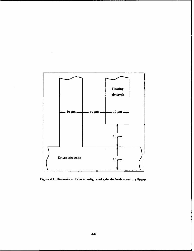
Floating-
electrode
10pam 10m 1M 0m
10 Jm
Driven-electrode 10 pmn
Figure 4.1. Dimensions of the interdigitated gate electrode structure fingers.
4-3
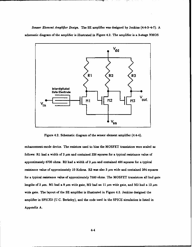
Sensor Element Amplifier Design. The SE amplifier was designed by Jenkins (4:4-3--4-7). A
schematic diagram of the amplifier is illustrated in Figure 4.2. The amplifier is a 3-stage NMOS
V dd
RI R2 R3
Gat# Electrode>V
Ml M2 M3 Vout
VS
Figure 4.2. Schematic diagram of the sensor element amplifier (4:4-4).
enhancement-mode device. The resistors used to bias the MOSFET transistors were scaled as
follows: RI had a width of 3 pm and contained 326 squares for a typical resistance value of
approximately 6700 ohms. R2 had a width of 3 pm and contained 486 squares for a typical
resistance value of approximately 10 Kohms. R3 was also 3 Am wide and contained 364 squares
for a typical resistance value of approximately 7500 ohms. The MOSFET transistors all had gate
lengths of 3 pm. M1 had a 9 pm wide gate, M2 had an 11 pm wide gate, and M3 had a 12 pm
wide gate. The layout of the SE amplifier is illustrated in Figure 4.3. Jenkins designed the
amplifier in SPICE3 (U.C. Berkeley), and the code used in the SPICE simulation is listed in
Appendix A.
4-4
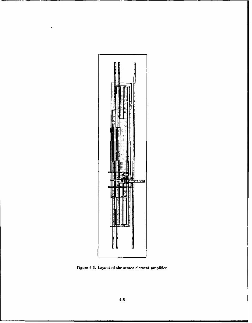
Figure 4.3. Layout of the sensor element amplifier.
4-5
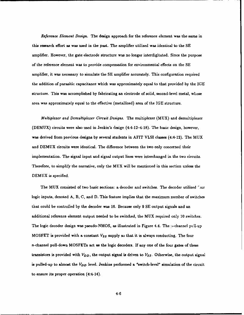
Reference Element Design. The design approach for the reference element was the same in
this research effort as was used in the past. The amplifier utilized was identical to the SE
amplifier. However, the gate electrode structure was no longer interdigitated. Since the purpose
of the reference element was to provide compensation for environmental effects on the SE
amplifier, it was necessary to simulate the SE amplifier accurately. This configuration required
the addition of parasitic capacitance which was approximately equal to that provided by the IGE
structure. This was accomplished by fabricating an electrode of solid, second-level metal, whose
area was approximately equal to the effective (metallized) area of the IGE structure.
Multiplexer and Demultiplerer Circuit Designs. The multiplexer (MUX) and demultiplexer
(DEMUX) circuits were also used in Jenkin's design (4:4-12-4-18). The basic design, however,
was derived from previous designs by several students in AFIT VLSI classes (4:4-12). The MUX
and DEMUX circuits were identical. The difference between the two only concerned their
implementation. The signal input and signal output lines were interchanged in the two circuits.
Therefore, to simplify the narrative, only the MUX will be mentioned in this section unless the
DEMUX is specified.
The MUX consisted of two basic sections: a decoder and switches. The decoder utilized %ur
logic inputs, denoted A, B, C, and D. This feature implies that the maximum number of switches
that could be controlled by the decoder was 16. Because only 9 SE output signals and an
additional reference element output needed to be switched, the MUX required only 10 switches.
The logic decoder design was pseudo-NMOS, as illustrated in Figure 4.4. The .f-channel pull-up
MOSFET is provided with a constant Vss supply so that it is always conducting. The four
n-channel pull-down MOSFETs act as the logic decoders. If any one of the four gates of these
transistors is provided with VDD, the output signal is driven to Vss. Otherwise, the output signal
is pulled-up to almost the VDD level. Jenkins performed a "switch-level" simulation of the circuit
to ensure its proper operation (4:4-14).
4-6
Vdd
Chem 1
VS
Figure 4.4. Schematic diagram of one bit-slice of the logic decoder (4:4-13).
An inverting buffer was also included in the design of the MUX circuit. The purpose of the
inverting buffer was to provide the correct logic levels for the operation of the switches at the
output of the MUX. It was necessary for the buffer to provide a control signal and its
complement, as illustrated in Figure 4.5. Since the decoder section of the MUX was designed in
pseudo-NMOS, the logic levels provided at its outputs were not exactly VDD and Vss.
Consequently, the buffer was used to restore the logic levels to VDD and Vss.
The final stage of the MUX circuit was a transmission gate (T-gate), and it is depicted in
Figure 4.6. Th,; purpose of the gate is to either pass the selected signal or block unselected
signals. Therefore, it acted as an analog switch. The only difference between the MUX and the
DEMUX was in the implementation of the input and output signa!-. That is, the MUX circuit
selected one of ten inputs and passed it to the output, while the DEMUX passed its input to one
of nine outputs. The controlling logic for this circuit was the output of the decoder section and its
complement, which were derived in the inverting buffer section. The gate dimensions of the
4-7
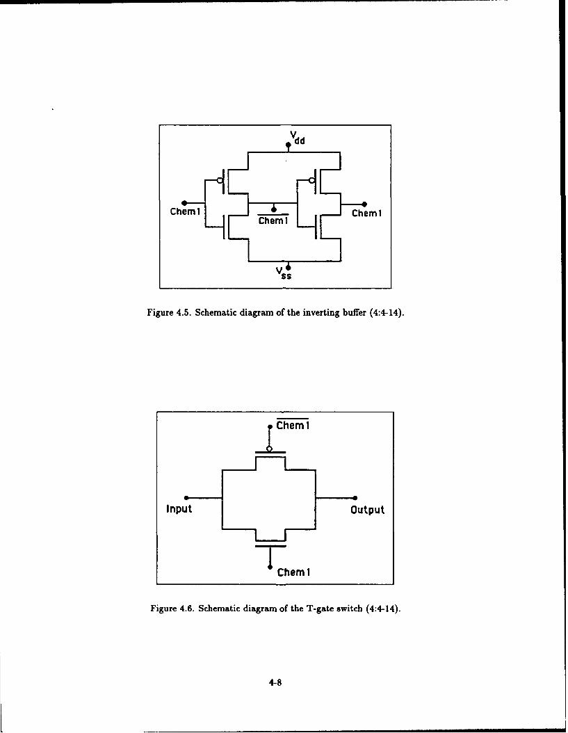
Vdd
ChemI ChemI
V 46
Figure 4.5. Schematic diagram of the inverting buffer (4:4-14).
jCheml
Input Output
Chem i
Figure 4.6. Schematic diagram of the T-gate switch (4:4-14).
4-8
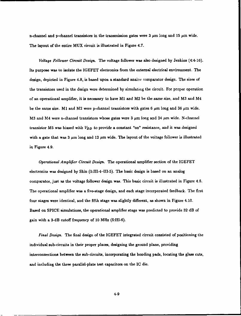
n-channel and p-channel transistors in the transmission gates were 3 pm long and 15 pm wide.
The layout of the entire MUX circuit is illustrated in Figure 4.7.
Voltage Follower Circuit Design. The voltage follower was also designed by Jenkins (4:4-16).
Its purpose was to isolate the IGEFET electronics from the external electrical environment. The
design, depicted in Figure 4.8, is based upon a standard analov comparator design. The sizes of
the transistors used in the design were determined by simulating the circuit. For proper operation
of an operational amplifier, it is necessary to have M1 and M2 be the same size, and M3 and M4
be the same size. Ml and M2 were p-channel transistors with gates 6 pm long and 36 pm wide.
M3 and M4 were n-channel transistors whose gates were 3 pm long and 24 pm wide. N-channel
transistor M5 was biased with VDD to provide a constant "on" resistance, and it was designed
with a gate that was 3 pm long and 12 pm wide. The layout of the voltage follower is illustrated
in Figure 4.9.
Operational Amplifier Circuit Design. The operational amplifier section of the IGEFET
electronics was designed by Shin (5:111-4-111-5). The basic design is based on an analog
comparator, just as the voltage follower design was. This basic circuit is illustrated in Figure 4.8.
The operational amplifier was a five-stage design, and each stage incorporated feedback. The first
four stages were identical, and the fifth stage was slightly different, as shown in Figure 4.10.
Based on SPICE simulations, the operational amplifier stage was predicted to provide 32 dB of
gain with a 3-dB cutoff frequency of 10 MHz (5:111-6).
Final Design. The final design of the IGEFET integrated circuit consisted of positioning the
individual sub-circuits in their proper places, designing the ground plane, providing
interconnections between the sub-circuits, incorporating the bonding pads, locating the glass cuts,
and including the three parallel-plate test capacitors on the IC die.
4-9
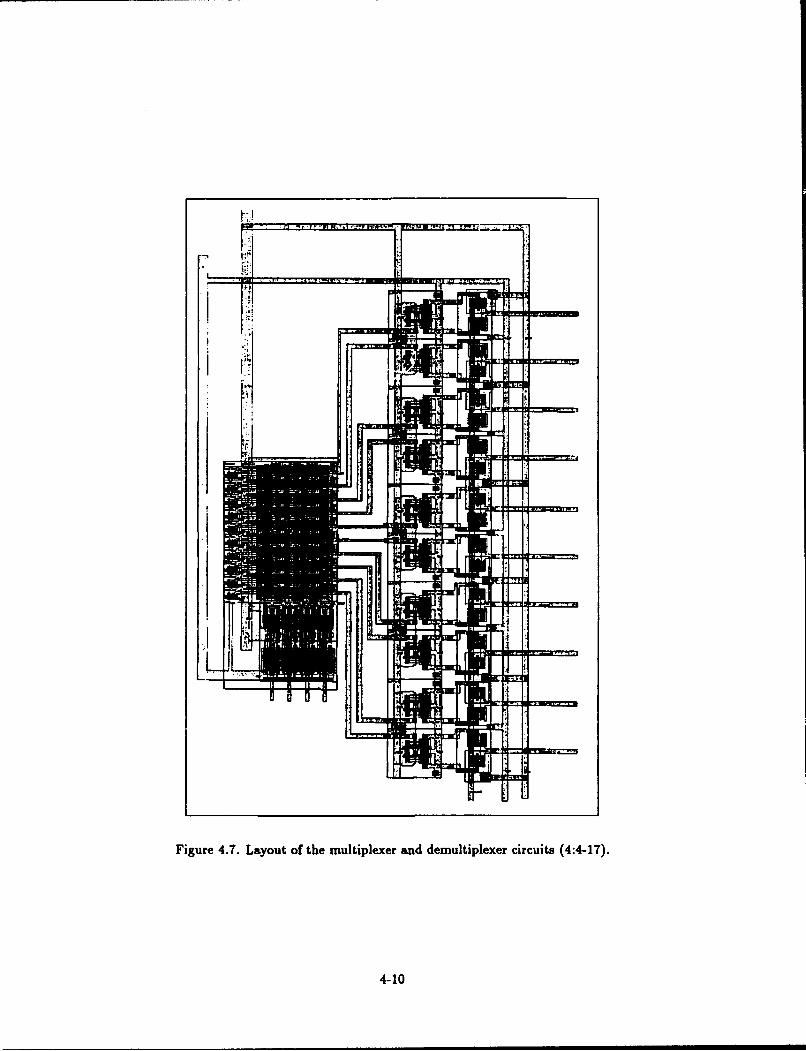
I.'
Figure 4.7. Layout of the multiplexer and demultiplexer circuits (4:4-17).
4-10
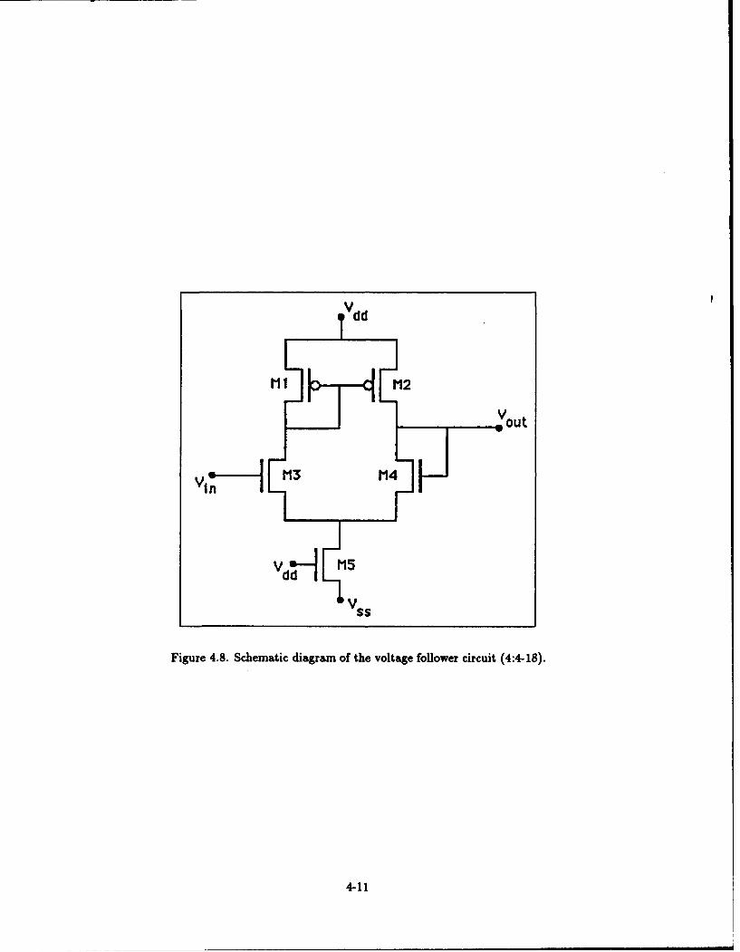
V dd
MI M2
Vout
v 1, M3 M4
VdH M5
Vss
Figure 4.8. Schematic diagram of the voltage follower circuit (4:4-18).
4-11
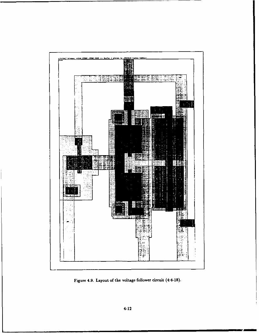
'
Fiur 4.9 Layou oftevltgaolwe sicit( 8
4-12 I-
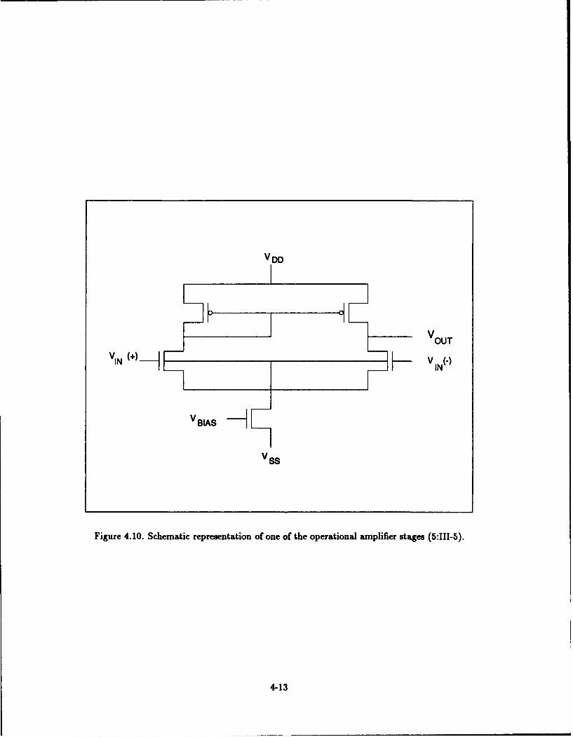
V DD
VIN FF IN
V
Figure 4.10. Schematic representation of one of the operational amplifier stages (5:111-5).
4-13
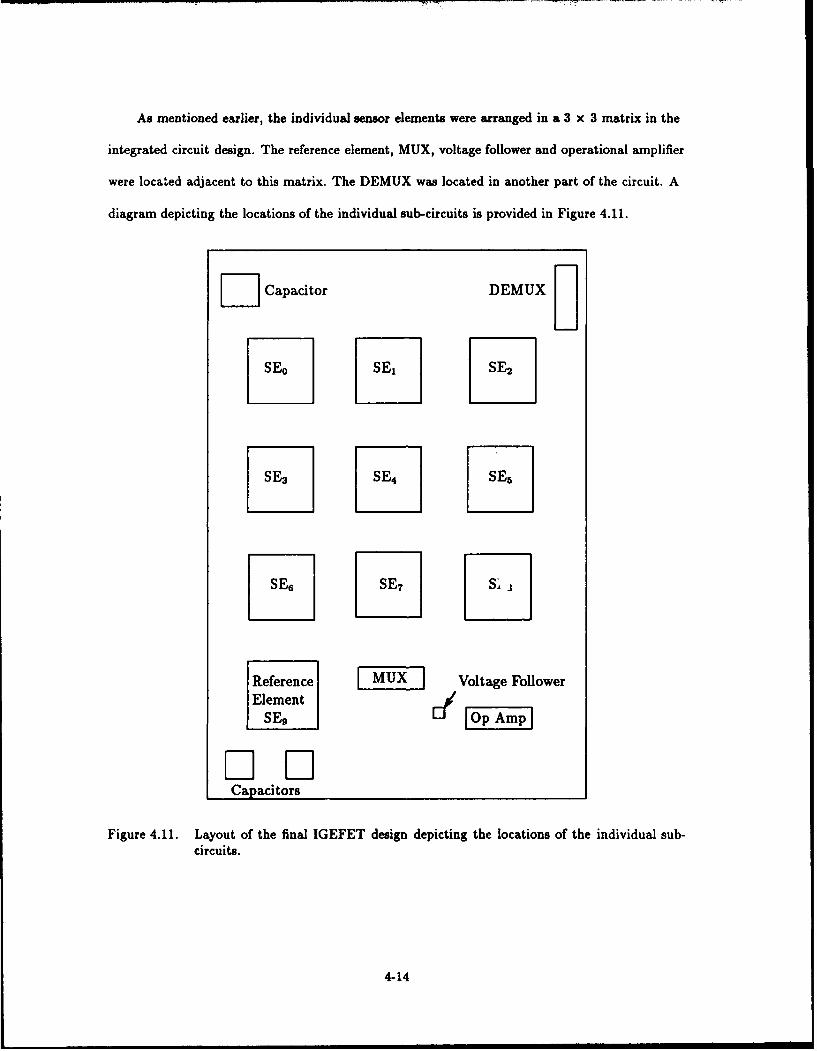
As mentioned earlier, the individual sensor elements were arranged in a 3 x 3 matrix in the
integrated circuit design. The reference element, MUX, voltage follower and operational amplifier
were located adjacent to this matrix. The DEMUX was located in another part of the circuit. A
diagram depicting the locations of the individual sub-circuits is provided in Figure 4.11.
D Capacitor DEMUX
SE0 SE, SE2
SE3 SE4 SEs
SE6 SE7 S1 3
Reference MUX Voltage FollowerElement J___
Capacitors
Figure 4.11. Layout of the final IGEFET design depicting the locations of the individual sub-circuits.
4-14
Glass cuts were placed in numerous areas on the integrated circuit. Their purpose was to
provide a means of troubleshooting internal nodes (those nodes not connected to bonding pads),
and to facilitate easy excision of inoperative circuits with an ultrasonic microprobe cutter.
Three capacitors, designed in first- and second-level metal, were located in different areas on
the die. They were all different sizes: one was 100 pm x 100 pm, the second was 200 Pm x 200
pm, and the third was 400 pm x 400 pm. Their purpose was to provide a means for accurately
measuring the thickness and electrical properties of the silicon dioxide layer fabricated between
the two metal layers.
Finally, bonding pads were located around the integrated circuit. Due to the large number of
nodes in the design that required bonding pads, some sacrifices were made. It would have been
preferable to provide separate power supply lines for each sub-circuit. In the final design,
however, most circuits shared a common power supply bus. Also, the operational amplifier design
required separate offset voltages for each stage. In the final design, all the offset voltage lines were
tied together.
IGEFET Integrated Circuit Fabrication. After the design was finalized, a CIF (Caltech
Intermediate Form) file was generated and forwarded to the Metal-Oxide-Semiconductor
Implementation System (MOSIS) for fabrication. The CIF file generated was for the 2 pm,
CMOS, n-well, double polysilicon fabrication technology. A photomicrograph of an IGEFET
integrated circuit received from MOSIS is presented in Figure 4.12. Twenty-five packaged
integrated circuits were received. The bonding pad arrangement and MOSIS parametric test
results are provided in Appendix B. The integrated circuit package pin assignments are listed in
Table 4.1.
The SPICE level-4 parameters for the integrated circuit, which were based upon the actual
characteristics of the fabricated devices, were included with the MOSIS parametric test results.
The SPICE level-4 transistor models necessary to simulate the circuit were derived from the
4-15
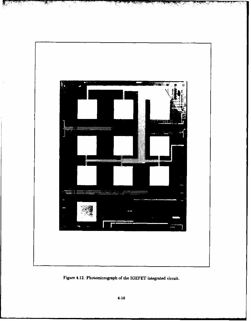
.77 P7-77
Figure 4.12. Photornicrograph of the IGEFET integrated circuit.
4-16
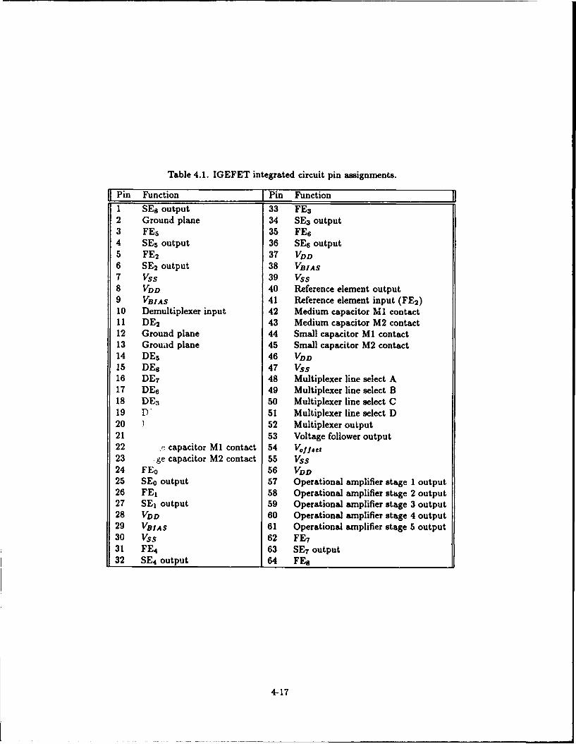
Table 4.1. IGEFET integrated circuit pin assignments.
Pin Function Pin Function
1 SES output 33 FE32 Ground plane 34 SE 3 output3 FE5 35 FE64 SE 5 output 36 SE 6 output5 FE 2 37 VDD6 SE 2 output 38 VBIAS
7 Vs$ 39 V$$8 VDD 40 Reference element output9 VBIAS 41 Reference element input (FE 2 )10 Demultiplexer input 42 Medium capacitor M1 contact11 DE 2 43 Medium capacitor M2 contact12 Ground plane 44 Small capacitor M1 contact13 Ground plane 45 Small capacitor M2 contact14 DE5 46 VDD15 DEs 47 Vss16 DE 7 48 Multiplexer line select A17 DE 6 49 Multiplexer line select B18 DE 3 50 Multiplexer line select C19 D 51 Multiplexer line select D20 1 52 Multiplexer output21 53 Voltage follower output22 e capacitor M1 contact 54 Volfset23 ge capacitor M2 contact 55 Vss24 FEO 56 VDD25 SE0 output 57 Operational amplifier stage 1 output26 FE, 58 Operational amplifier stage 2 output27 SE, output 59 Operational amplifier stage 3 output28 VDD 60 Operational amplifier stage 4 output29 VDIAS 61 Operational amplifier stage 5 output30 Vss 62 FE 731 FE4 63 SE 7 output32 SE 4 output 64 FEs
4-17
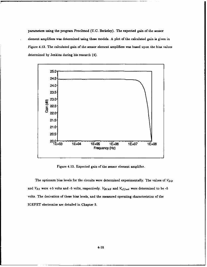
parameters using the program Proc2mod (U.C. Berkeley). The expected gain of the sensor
element amplifiers was determined using these models. A plot of the calculated gain is given in
Figure 4.13. The calculated gain of the sensor element amplifiers was based upon the bias values
determined by Jenkins during his research (4).
25.0-
24.5-
24.0-
23.5-
23.0-
" 22.5-
22.0-
21.5-
21.0-
20.5-
0E &...... E......+05 . 1,E+06 . 1 07 1 EFrequency (Hz)
Figure 4.13. Expected gain of the sensor element amplifier.
The optimum bias levels for the circuits were determined experimentally. The values of VDD
and Vss were +5 volts and -5 volts, respectively. VDIAS and Vol fet were determined to be -5
volts. The derivation of these bias levels, and the measured operating characteristics of the
IGEFET electronics are detailed in Chapter 5.
4-18
IGEFET Performance Instrumentation Configuration
The configuration of the electrical test equipment used to accomplish the measurements of
the IGEFET's performance during the resin cure experiments is discussed in this section.
General Considerations. Several different electrical measurements were conducted during
the resir cure experiments. These measurements included:
1. Direct current (dc) resistance of the IGE structure.
2. Alternating current (ac) impedance (magnitude and phase) of the IGE structure.
3. Gain and phase delay of the IGE structure.
4. Gain and phase delay of the IGEFET.
5. Gain and phase delay of the reference element.
6. Time-domain response of the IGEFET to a voltage pulse excitation.
7. Frequency-domain response of the IGEFET to a voltage pulse excitation.
In order to maximize the number of measurements performed during the resin's cure cycle, a
separate cure was performed for each electrical measurement detailed above. Each different
electrical measurement, therefore, constituted a separate resin cure experiment. In addition, since
the resin was cured at two temperatures, two experiments were performed for each different
electrical measurement-one experiment for each cure temperature. All electrical measurements
were referenced relative to the elapsed time during the resin's cure cycle. Also, the resins were
cured until the elapsed time of the experiment was at least double the time required to achieve
the estimated gelation point.
A Zenith model 248 microcomputer (Zenith Data Systems, St. Joseph, MI) was used to
collect the data. Control of the test equipment and retrieval of the performance data was
facilitated by and IEEE-488 interface card (Capitol Equipment Corp., model 01000-60300,
4-19
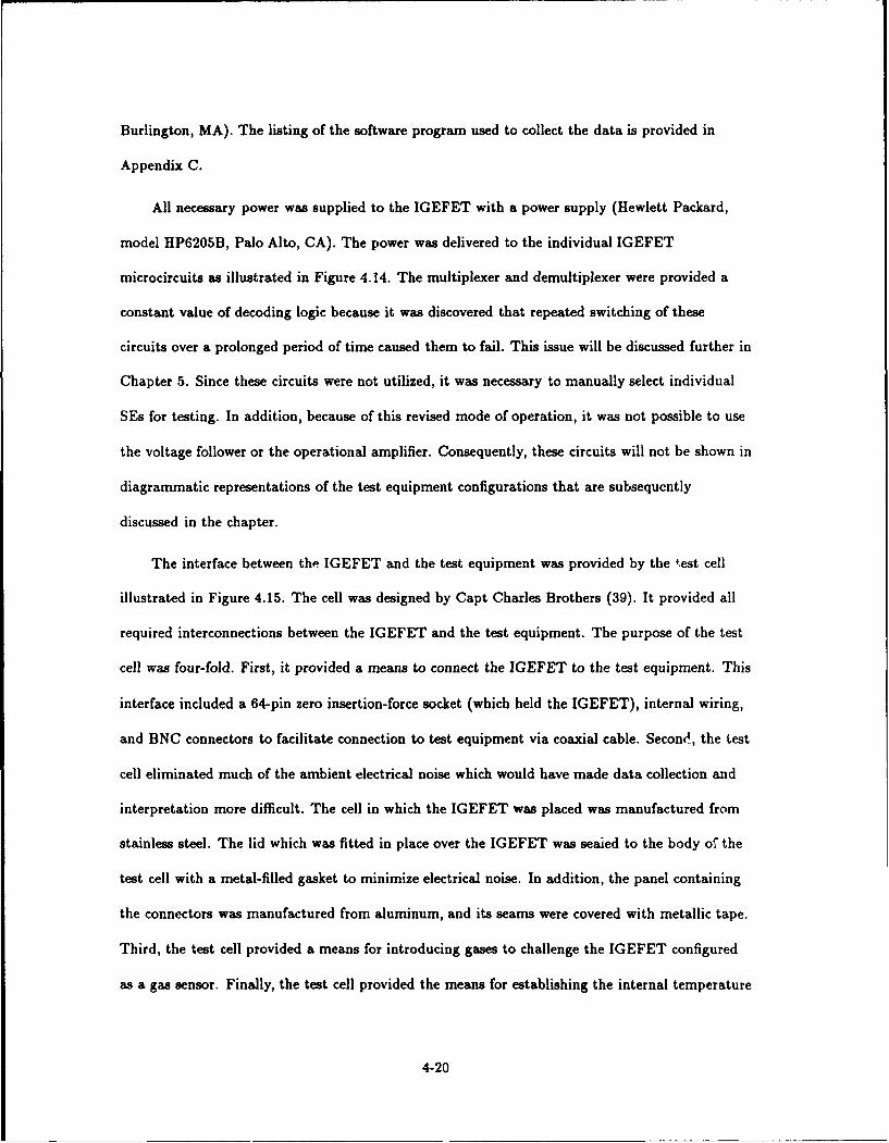
Burlington, MA). The listing of the software program used to collect the data is provided in
Appendix C.
All necessary power was supplied to the IGEFET with a power supply (Hewlett Packard,
model HP6205B, Palo Alto, CA). The power was delivered to the individual IGEFET
microcircuits as illustrated in Figure 4.14. The multiplexer and demultiplexer were provided a
constant value of decoding logic because it was discovered that repeated switching of these
circuits over a prolonged period of time caused them to fail. This issue will be discussed further in
Chapter 5. Since these circuits were not utilized, it was necessary to manually select individual
SEs for testing. In addition, because of this revised mode of operation, it was not possible to use
the voltage follower or the operational amplifier. Consequently, these circuits will not be shown in
diagrammatic representations of the test equipment configurations that are subsequently
discussed in the chapter.
The interface between the IGEFET and the test equipment was provided by the test cell
illustrated in Figure 4.15. The cell was designed by Capt Charles Brothers (39). It provided all
required interconnections between the IGEFET and the test equipment. The purpose of the test
cell was four-fold. First, it provided a means to connect the IGEFET to the test equipment. This
interface included a 64-pin zero insertion-force socket (which held the IGEFET), internal wiring,
and BNC connectors to facilitate connection to test equipment via coaxial cable. Second4, the test
cell eliminated much of the ambient electrical noise which would have made data collection and
interpretation more difficult. The cell in which the IGEFET was placed was manufactured from
stainless steel. The lid which was fitted in place over the IGEFET was seaied to the body or, the
test cell with a metal-filled gasket to minimize electrical noise. In addition, the panel containing
the connectors was manufactured from aluminum, and its seams were covered with metallic tape.
Third, the test cell provided a means for introducing gases to challenge the IGEFET configured
as a gas sensor. Finally, the test cell provided the means for establishing the internal temperature
4-20
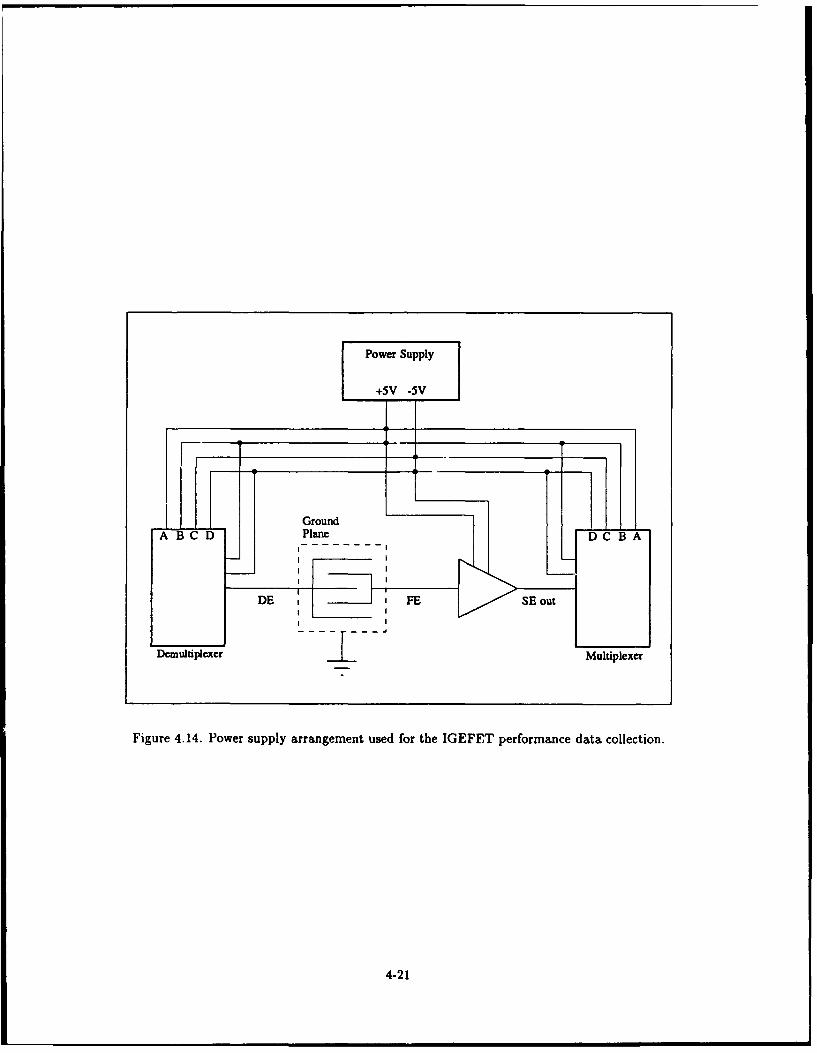
Power Supply
+5V -5V
DE S u
Dernultiplexer Multiplexer
Figure 4.14. Power supply arrangement used for the IGEFET performance data collection.
4-21
OhI*no
0, 0 0
0
Challenge . a * a a
a Input
Integrated circuit ToP ViewSeniar Placed Tira
Inalde the ChaMber Strip G.Otu
I1np 1* Teat Chamber
Patch* * * * *.0PsnotPae
4 6 5 6 O 0
Side View
Front View
Figure 4.15. Diagram of the IGEFET test cell (39:9).
4-22
of the test environment. The cell contained a thermocouple (Omega Engineering, Inc., model
SA1-K, Stanford, CT) and a kapton heater strip (Watlow, modl 'ACC5020C5, St. Louis, MO),
which were attached to the top of the zero insertion-force socket. The IGEFET was then placed
in the socket in direct contact with these devices.
During the resin cure experiments, it was necessary to strictly control the humidity in the
test cell. Humidity is a factor which can significantly affect the mechanical properties of resins
(40). The humidity level was controlled by providing a constant flow of nitrogen through the test
cell. The flow was provided by a gas generation and delivery system which was developed by
Kolesar (41). The system was used to regulate the flow of nitrogen into the test cell at
approximately 250 ml/min. This flow kept the humidity level in the test cell below 5 percent
during all experiments. The humidity level was monitored by a hygrometer (Thunder Scientific
Corp., model HS-1CHDT-2A, Albuquerque, NM).
Electrical Performance Instrumentation Configurations. The following sections detail the
IGEFET electrical performance measurement test equipment configurations.
Direct Current Resistance Measurements. The dc resistance of the IGE structure was
measured using an electrometer (Keithly Instruments, Inc., Model 617, Cleveland, OH). The
equipment was arranged as illustrated in Figure 4.16. The electrometer was operated in a
(V/I)-mode to minimize the effects of leakage resistance and distributed capacitance. This mode
of operation also facilitates the measurement of resistances on the order of 1016 ohms (42). The
dc resistance was measured and recorded with respect to applied bias and time. No power was
applied to the IGEFET electronics during these measurements. To measure the dc resistance with
respect to the applied bias, the voltage source of the electrometer was increased in 1-volt
increments over the interval of 2 volts to 10 volts. Measurements of dc resistance with respect to
time were accomplished by recording the resistance of the IGE structure with a 2-volt applied
bias, and referencing the measurement to the elapsed time relative to the resin's cure cycle. Prior
4-23
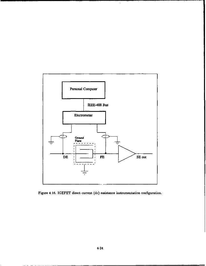
Electrometer JPlane
DE I FE SE outI >I
Figure 4.16. IGEFET direct current (dc) resistance instrumentation configuration.
4-24
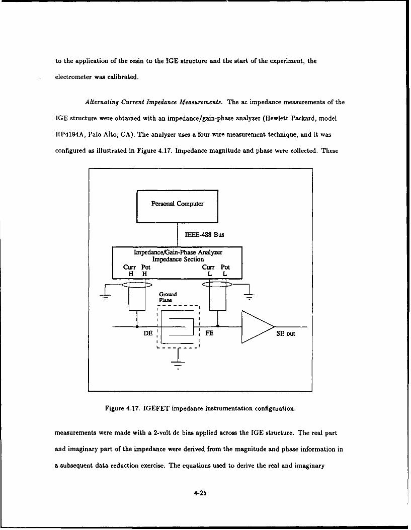
to the application of the resin to the IGE structure and the start of the experiment, the
electrometer was calibrated.
Alternating Current Impedance Measurements. The ac impedance measurements of the
IGE structure were obtained with an impedance/gain-phase analyzer (Hewlett Packard, model
HP4194A, Palo Alto, CA). The analyzer uses a four-wire measurement technique, and it was
configured as illustrated in Figure 4.17. Impedance magnitude and phase were collected. These
Personal Computer
IEEE-488 Bus
Irnpedance/Gain-Phase AnalyzerImpedance Section
Curr Pot Curr PotH H L L
L_
Figure 4.17. IGEFET impedance instrumentation configuration.
measurements were made with a 2-volt dc bias applied across the IGE structure. The real part
and imaginary part of the impedance were derived from the magnitude and phase information in
a subsequent data reduction exercise. The equations used to derive the real and imaginary
4-25
components of the impedance (Re(Z) and Ir(Z), respectively) were:
Re(Z) I COS (4.1)
and,
Im(Z) =IZI sin4, (4.2)
where I Z I is the impedance magnitude, and 0 is the impedance phase. Measurements were
accomplished with respect to frequency, which was varied from 100 Hz to 100 KHz. Prior to the
start of each impedance experiment, a short-circuit calibration was performed by inserting a
jumper wire across the zero insertion-force socket pins corresponding the DE and the FE of the
IGE structure. An open-circuit calibration was also performed.
Gain-Phase Measurements. The gain and phase delay of the IGE structure and the
IGEFET were also measured with the impedance/gain-phase analyzer (Hewlett Packard, model
HP4194A, Palo Alto, CA). The test equipment configuration is depicted in Figure 4.18. Since the
electrical characteristics of the resin varied considerably over the course of its cure, it was
necessary to manually vary the magnitude of the input signal. A correctly adjusted signal level
would provide a favorable signal-to-noise ratio without overloading the analyzer's input. At the
beginning of cure, the magnitude of the analyzer's oscillator signal was set at 0.01 volts, and it
was gradually increased during successive measurements to a final value of 1 volt. The voltage
gain (20 log 0[Vt/V,.]) and phase delay (4.t - Oi.) were measured over a frequency range of 10
Hz to 1 KHz. The analyzer was calibrated at the start of each measurement cycle.
Time-Domain Response Measurements. The time-domain response of the IGEFET to a
voltage pulse excitation was measured utilizing the configuration illustrated in Figure 4.19. The
measurements were made by applying the voltage pulse to the driven-electrode of the IGE
structure using a function generator (Wave-Tek Corp., model 148, San Diego, CA) and recording
4-26
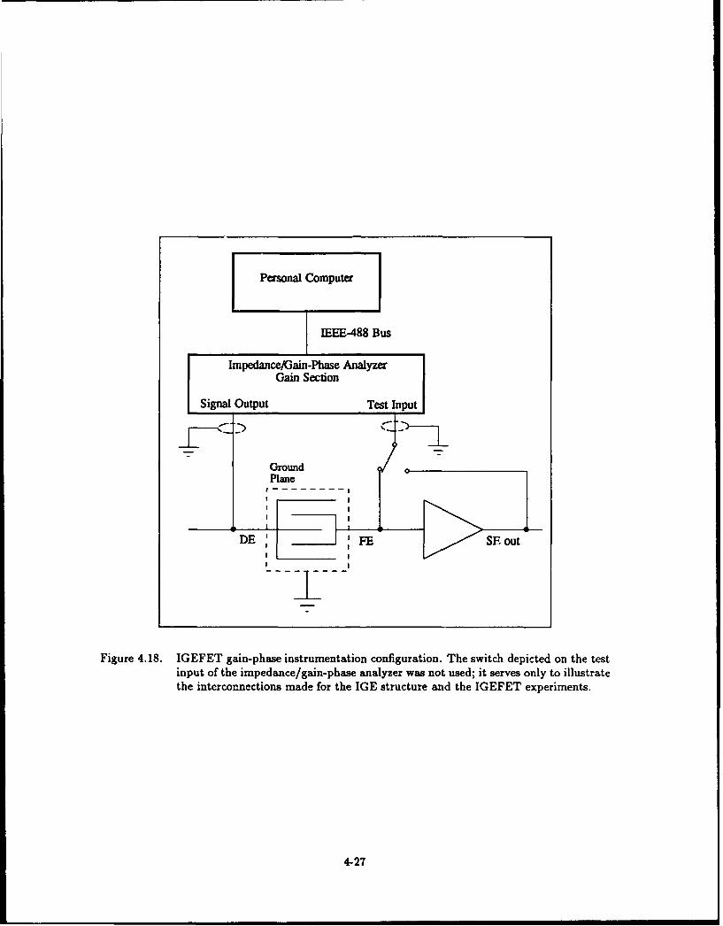
Personal Computer
IEEE-488 Bus
DEFE SE out
Figure 4.18. IGEFET gain-phase instrumentation configuration. The switch depicted on the testinput of the impedance/gain-phase analyzer was not used; it serves only to illustratethe interconnections made for the IGE structure and the IGEFET experiments.
4-27
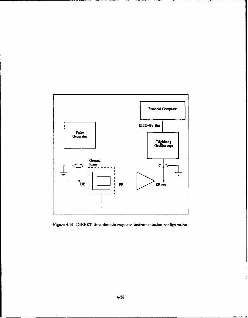
Personal Computer
IEEE-488 Bus
PulseGenerator
DigitizingOscilloscope
Ground
DE7~ FES u
L -
Figure 4.19. IGEFET time-domain response instrumentation configuration.
4-28
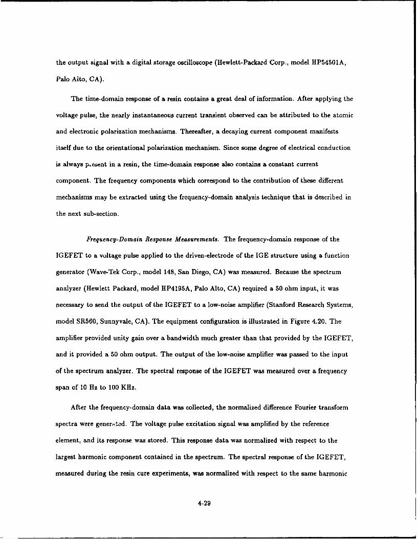
the output signal with a digital storage oscilloscope (Hewlett-Packard Corp., model HP54501A,
Palo Alto, CA).
The time-domain response of a resin contains a great deal of information. After applying the
voltage pulse, the nearly instantaneous current transient observed can be attributed to the atomic
and electronic polarization mechanisms. Thereafter, a decaying current component manifests
itself due to the orientational polarization mechanism. Since some degree of electrical conduction
is always pesent in a resin, the time-domain response also contains a constant current
component. The frequency components which correspond to the contribution of these different
mechanisms may be extracted using the frequency-domain analysis technique that is described in
the next sub-section.
Frequency-Domain Response Measurements. The frequency-domain response of the
IGEFET to a voltage pulse applied to the driven-electrode of the IGE structure using a function
generator (Wave-Tek Corp., model 148, San Diego, CA) was measured. Because the spectrum
analyzer (Hewlett Packard, model HP4195A, Palo Alto, CA) required a 50 ohm input, it was
necessary to send the output of the IGEFET to a low-noise amplifier (Stanford Research Systems,
model SR560, Sunnyvale, CA). The equipment configuration is illustrated in Figure 4.20. The
amplifier provided unity gain over a bandwidth much greater than that provided by the IGEFET,
and it provided a 50 ohm output. The output of the low-noise amplifier was passed to the input
of the spectrum analyzer. The spectral response of the IGEFET was measured over a frequency
span of 10 Hz to 100 KHz.
After the frequency-domain data was collected, the normalized difference Fourier transform
spectra were gener..ted. The voltage pulse excitation signal was amplified by the reference
element, and its response was stored. This response data was normalized with respect to the
largest harmonic component contained in the spectrum. The spectral response of the IGEFET,
measured during the resin cure experiments, was normalized with respect to the same harmonic
4-29
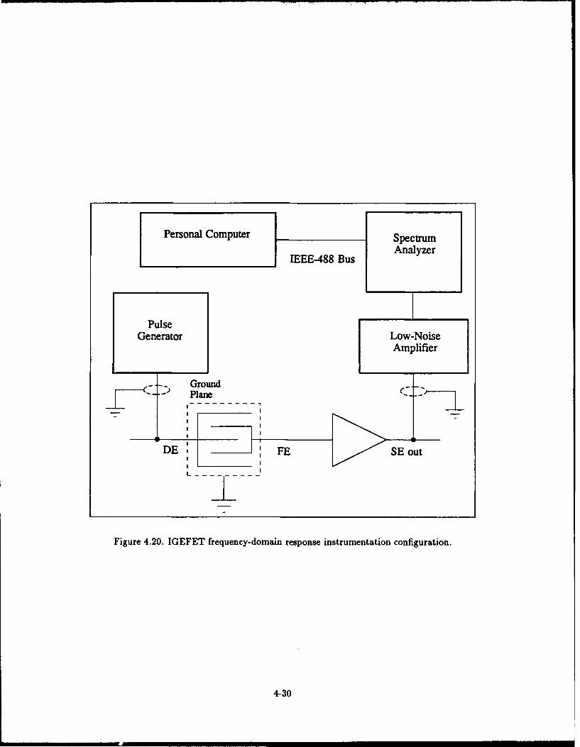
PersnalCompterSpectrum
EEEE-488 Bus Analyzer
PulseTGenerator Low-Noise
Amplifier
~ {) Plane
DEFE > Sou
Figure 4.20. IGEFET frequency-domain response instrumentation configuration.
4-30
identified from the spectrum of the voltage pulse excitation. The normalized difference Fourier
transform spectrum was then calculated by subtracting the normalized IGEFET response from
the normalized reference element response, and taking the absolute value of the difference.
Consequently, this spectrum provides information regarding the dissipation of energy in the
IGE-resin system with respect to the voltage pulse excitation signal.
Experimental Methodology
As discussed in Chapter 1, the IGE structure and IGEFET electrical measurements were
performed at two different cure temperatures. These two cure temperatures were determined
empirically. The total experimental effort was not simply the collection of electrical performance
measurements. That is, prior to conducting the electrical tests, it was necessary to evaluate the
mechanical properties of the resin to determine the most advantageous resin cure temperatures.
Consequently, this section is divided into two sub-sections; the first will discuss the experimental
methodology used during the collection of the mechanical data, and the second is concerned with
the evaluation of the IGEFET sensor.
Mechanical Test Procedures. As previously mentioned, prior to the evaluation of the
IGEFET sensor as a resin cure monitor, it was necessary to determine the most advantageous
resin cure temperatures. From a purely experimental perspective, the temperatures were selected
based upon three criteria. First, the temperatures could not be so large as to damage the test
cell. Based on the maximum temperature that the zero insertion-force socket could withstand, it
was determined that the maximum allowable resin cure temperature was approximately 1000C.
Second, the temperatures needed to be sufficiently low to provide a useful amount of data. An
excessively high cure temperature would cause the resin to cure too quickly, and this situation
would compromise the collection of a useful data. Third, the temperatures needed to be
sufficiently large to prevent inordinately long cure times.
4-31
The.bptimum cure temperatures were determined using a dynamic spectrometer
(Rheometrics Inc., model RDS-11, Possumtown, Piscataway, NJ). The dynamic spectrometer
applies an oscillatory, sinusoidal motion tc, a sample of resin placed between a pair of parallel
plates that are 1.25 inches in diameter. The force is applied directly to the lower plate, and it is
transmitted through the resin to the upper plate. A sensor attached to the upper plate measures
the amount of force transmitted through the resin.
A sample of the Epoxy 907 resin was prepared according to the vendor's instructions
included with the resin: equal amounts of components A and B were applied to a clean,
disposable surface (a piece of paper), and they were mixed together for at least three minutes
with a wooden tongue depressor. A sufficient amount of the resin (approximately 2 mm thick)
was applied to provide a uniform layer between the two plates. The plates were then transferred
to an oven under a nitrogen atmosphere to reduce the level of humidity. The oven was then
programmed to follow a ramped temperature profile, from room temperature to approximately
1300C, at a rate of 20C per minute. During the cure of the resin, the lower plate was oscillated at
a rate of 10 rad/s. The resultant data, complex viscosity (1*) versus temperature, was analyzed
to determine the optimum range of cure temperatures for the resin. Two of these temperatures
were selected based upon the three criteria discussed above.
After the resin cure temperatures to be used during the IGEFET sensor evaluation were
selected, it was necessary to determine the gelation time of the resin at each of these
temperatures. The dynamic spectrometer was again used, and the procedure was similar to that
described above, with the exception that the temperature was programmed to follow an
isothermal profile rather than a ramped profile. One isothermal evaluation was performed for
each temperature used during the IGEFET sensor evaluation. The data collected was the storage
modulus (G') and the loss modulus (G"). The storage modulus and loss modulus correspond to
the real part and the imaginary part, respectively, of the resin's complex viscosity. This
4-32
information was plotted with respect to time, and the point at which G' = G" was located. This
point corresponds to the gelation time of the resin (13).
It is noted here that oscillating the sample at frequencies other than 10 rad/s would result in
different interpretations of the gelation time, since the amount of force transmitted through the
sample depends upon the rate at which the sample is oscillated. It has been determined
empirically, however, that the frequency which provides the best agreement with the actual
gelation time is 10 rad/s (13).
A third mechanical test was used to determine the glass transition temperature of the resin.
Again, the dynamic spectrometer was used. This time, however, the spectrometer was confgured
to perform a torsional bar analysis (TBA) of samples cured at each of the two temperatures of
interest. Small bars of the resin were made by preparing samples of the resin and placing them in
molds made from RTV silicone (General Electric Co., Silicone Products Division, product code
RTV664, Waterford, NY). The samples were then cured at the temperatures of interest. The bars
were approximately 3 mm high, 13 mm wide, and 42 mm long.
To conduct the TBA, a pair of clamps were substituted for the plates used in the parallel
plate tests, and a resin bar was secured with the clamps (a clamp held each end of the bar). The
clamps and bar were then enclosed in an oven under a nitrogen atmosphere to reduce the
humidity. A 10 rad/s oscillatory motion was applied to the bar, and the oven was thermostatted
to the temperature of interest. The storage modulus, loss modulus and the mechanical loss
tangent (tan 6 , = G"/G') were collected and plotted versus time.
IGEFET Test Procedures. The purpose of this sub-section is to detail the procedures used
to collect the IGEFET electrical performance data. In general, the process included preparation
of the sensor for the application of the resin, testing each sensor element for correct operation,
application of the resin, and collection of the data. These steps are detailed in the following
sub-sections.
4-33
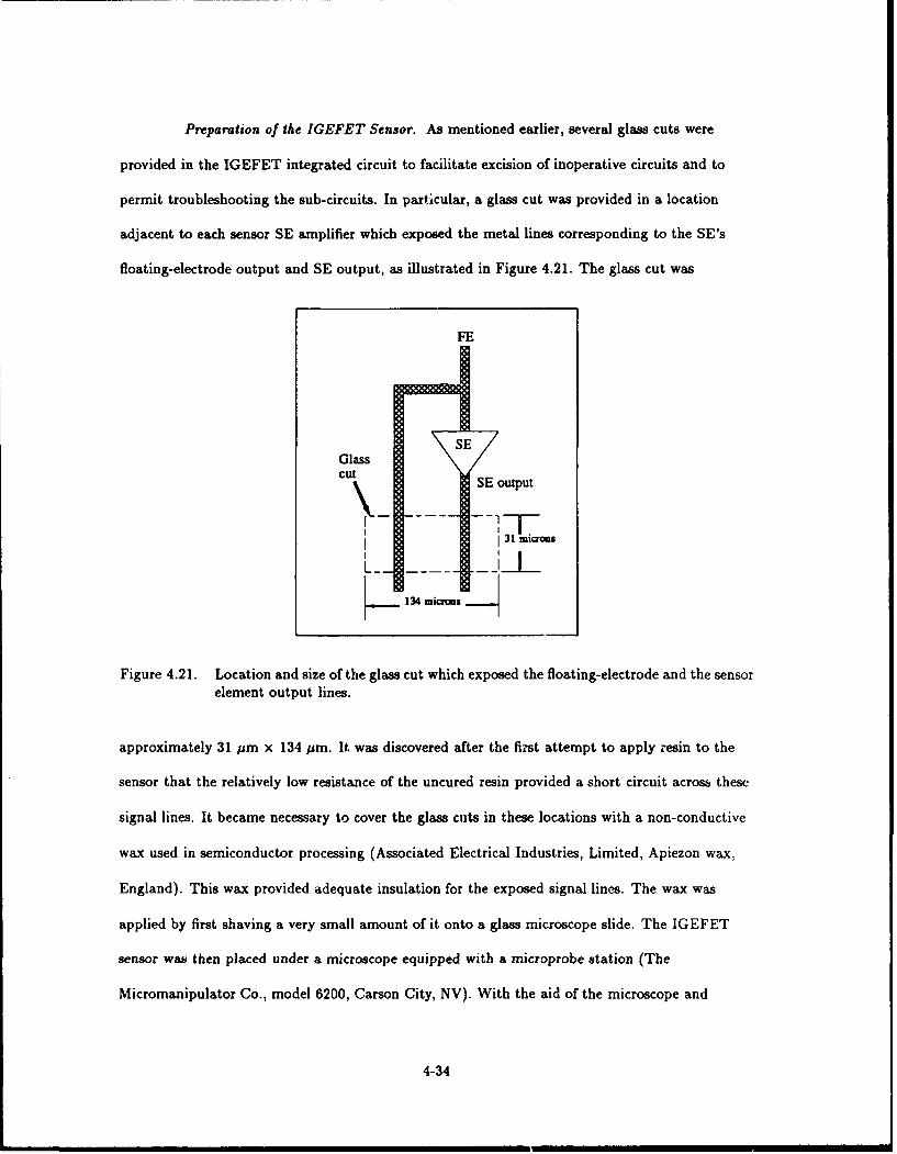
Preparation of the IGEFET Sensor. As mentioned earlier, several glass cuts were
provided in the IGEFET integrated circuit to facilitate excision of inoperative circuits and to
permit troubleshooting the sub-circuits. In particular, a glass cut was provided in a location
adjacent to each sensor SE amplifier which exposed the metal lines corresponding to the SE's
floating-electrode output and SE output, as illustrated in Figure 4.21. The glass cut was
FE
Glasscut SE output
... i...
134 miamos
Figure 4.21. Location and size of the glass cut which exposed the floating-electrode and the sensorelement output lines.
approximately 31 pm x 134 pm. It was discovered after the first attempt to apply resin to the
sensor that the relatively low resistance of the uncured resin provided a short circuit across these
signal lines. It became necessary to cover the glass cuts in these locations with a non-conductive
wax used in semiconductor processing (Associated Electrical Industries, Limited, Apiezon wax,
England). This wax provided adequate insulation for the exposed signal lines. The wax was
applied by first shaving a very small amount of it onto a glass microscope slide. The IGEFET
sensor was then placed under a microscope equipped with a microprobe station (The
Micromanipulator Co., model 6200, Carson City, NV). With the aid of the microscope and
4-34
probes, a shard of the wax was manipulated into position above each glass cut adjacent to a
sensor element. After each glass cut was covered by one or more pieces of wax, the integrated
circuit was placed in a piece of aluminum foil such that all the pins on the circuit protruded
through the foil. The integrated circuit was then placed in an oven (Lab-Line Instruments, Inc.,
model Imperial IV, Melrose Park, IL), and the temperature was thermostatted to approximately
850C to melt the wax over the glass cut.
Sensor Element Testing. Following the preparation of the integrated circuit for the
application of the resin, each SE on the integrated circuit was evaluated for proper operation.
This process involved visual and electrical inspection of the IGE structures and electrical testing
of each SE amplifier.
The IGE structures were visually inspected under the microscope of a microprobe station.
Obvious defects in an IGE structure, such as scratches, disqualified the associated SE from
further test and evaluation.
Following the visual inspection, the IGE structures were electrically evaluated using the
gain-phase mode of the impedance/gain-phase analyzer. The FE and DE of each structure were
expected to be isolated from each other by at least 30 dB relative to the frequency range which
spanned 10 Hz to 1 MHz.
The SE amplifiers on the integrated circuit were then electrically inspected. They were
expected to provide at least 17 dB of gain with a 3-dB cutoff frequency of at least 80 KHz.
Data Collection. The IGEFET performance evaluation process consisted of fourteen
experiments. Each of these experiments required a sample of resin to be deposited on the surface
of an IGE structure. While the resin sample cured, a single category of electrical measurement
was performed continuously. There were seven types of electrical measurements to be performed,
as discussed earlier in this chapter. In addition, the resin cure was evaluated at two different cure
4-35
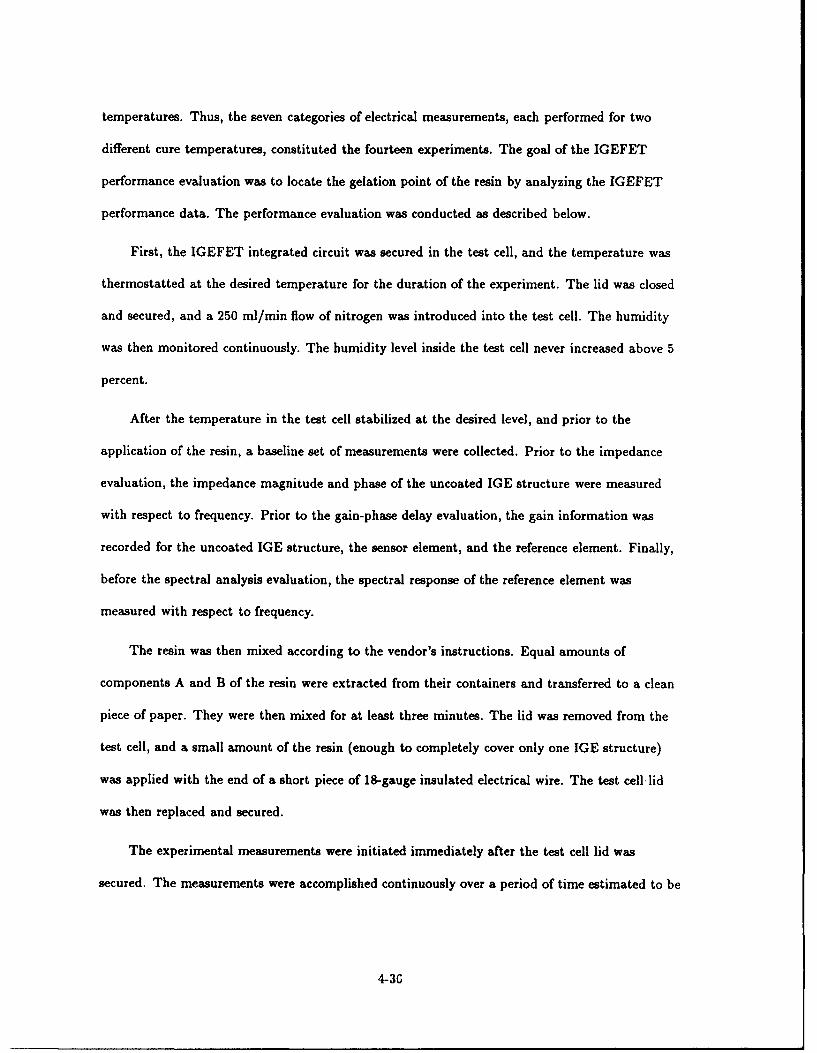
temperatures. Thus, the seven categories of electrical measurements, each performed for two
different cure temperatures, constituted the fourteen experiments. The goal of the IGEFET
performance evaluation was to locate the gelation point of the resin by analyzing the IGEFET
performance data. The performance evaluation was conducted as described below.
First, the IGEFET integrated circuit was secured in the test cell, and the temperature was
thermostatted at the desired temperature for the duration of the experiment. The lid was closed
and secured, and a 250 ml/min flow of nitrogen was introduced into the test cell. The humidity
was then monitored continuously. The humidity level inside the test cell never increased above 5
percent.
After the temperature in the test cell stabilized at the desired level, and prior to the
application of the resin, a baseline set of measurements were collected. Prior to the impedance
evaluation, the impedance magnitude and phase of the uncoated IGE structure were measured
with respect to frequency. Prior to the gain-phase delay evaluation, the gain information was
recorded for the uncoated IGE structure, the sensor element, and the reference element. Finally,
before the spectral analysis evaluation, the spectral response of the reference element was
measured with respect to frequency.
The resin was then mixed according to the vendor's instructions. Equal amounts of
components A and B of the resin were extracted from their containers and transferred to a clean
piece of paper. They were then mixed for at least three minutes. The lid was removed from the
test cell, and a small amount of the resin (enough to completely cover only one IGE structure)
was applied with the end of a short piece of 18-gauge insulated electrical wire. The test cell lid
was then replaced and secured.
The experimental measurements were initiated immediately after the test cell lid was
secured. The measurements were accomplished continuously over a period of time estimated to be
4-3C
double that of the resin sample's gelation time. The time periods were limited in this manner
because th electrical characteristics of the resin changed very little beyond the gelation point.
Summary
The details of the IGEFET design effort, the performance data collection configuration, and
experimental methodology were presented in this chapter. The IGEFET design effort was an
exercise in combining several features from previously successful designs while incorporating a
limited number of changes. An outline of the changes, and the details of the final IGEFET design
were discussed. A comprehensive description of the performance data collection configuration was
developed in the next section. Finally, the experimental procedures for the collection of the
mechanical and electrical performance data were described.
4-37
V. Results and Discussion
Introduciion
This chapter contains the results of the IGEFET sensor fabrication, the mechanical
characterization of the resin, and the resin cure experiments. Each of these phases of the
experimental process is discussed in a separate section. The first section presents the electrical
characteristics of the IGEFET sensor as received from MOSIS. The second section discusses the
results of the mechanical characterization of the resin used in this research. Finally, the third
section discusses the results of each of the electrical measurements performed during the resin
cure experiments.
Electrical Characteristics of the IGEFET Sensor
A visual and electrical inspection of the IGEFET sensor was performed immediately upon
receipt of the integrated circuits from MOSIS. The visual inspection was intended to identify any
obvious defects in the sensor. Of particular importance was the condition of the IGE structure.
Scratches on the surface of the structure could result in a short circuit between the DE and FE,
or they could cause large portions of the electrodes to be electrically isolated from the IGE
structure. In general, the condition of the IGE structures was acceptable, although occasional
scratches, possibly caused by the wire bonding and packaging processes, were observed.
In order to operate the IGEFET sensor's electronic sub-circuits, values for VDD, Vss, VEJAS,
and Voiijet had to be established. These values were determined empirically. It was assumed that
VDD would be in the vicinity of 5 volts, and that Vss and VEJAS would be in the vicinity of -5
volts. In order to simplify the power supply requirements, it was desirable to use the same
positive and negative voltage levels throughout the sub-circuits. The values for VDD, Vss, and
VBIAS were experimentally determined by adjusting their values to maximize the gain of the SE
amplifier. It was determined that using a value of 5 volts for VDD, and -5 volts for Vss and
5-1
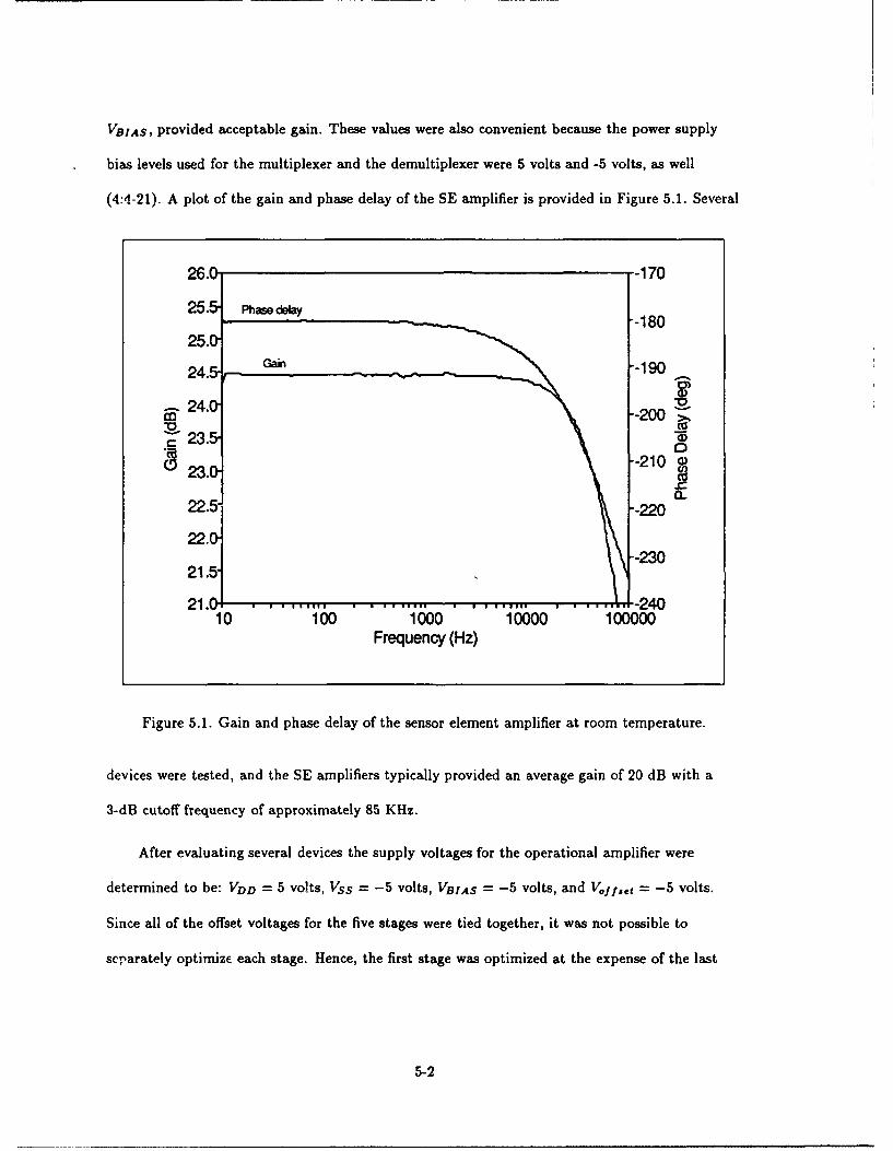
VBIAS, provided acceptable gain. These values were also convenient because the power supply
bias levels used for the multiplexer and the demultiplexer were 5 volts and -5 volts, as well
(4:4-21). A plot of the gain and phase delay of the SE amplifier is provided in Figure 5.1. Several
26.0- -170
25.5- Phase dewy-180
2 5 .0 " ai
24.5- G-190
24.0 m --200
C 23.5-
--210 aS23.0-
2D --230
21.0 .... .... 24010 10'0 10O00 "6600 10000
Frequency (Hz)
Figure 5.1. Gain and phase delay of the sensor element amplifier at room temperature.
devices were tested, and the SE amplifiers typically provided an average gain of 20 dB with a
3-dB cutoff frequency of approximately 85 KHz.
After evaluating several devices the supply voltages for the operational amplifier were
determined to be: VDD = 5 volts, VS = -5 volts, VBJAS = -5 volts, and Vojef " = -5 volts.
Since all of the offset voltages for the five stages were tied together, it was not possible to
separately optimize each stage. Hence, the first stage was optimized at the expense of the last
5-2
four. The first stage of the operational amplifier provided an average gain of 20 dB with a 3-dB
cutoff frequency of 850 KHz.
The voltage-follower circuits did not operate as expected. With the supply voltages
configured as described, the gain of the sub-circuit (measured with respect to a signal placed on
the FE of the sensor element) was typically on the order of -6 dB. By increasing the supply
voltages to 5.5 volts and -5.5 volts, the gain could be increased to approximately 10 dB. This was
considered unacceptable. Since the SE amplifiers each had their own output, which could be
accessed via the multiplexer, the failure of the voltage-follower circuits to operate acceptably was
not considered to be a critical defect.
Once the voltage bias levels necessary to operate the sub-circuits were determined, the
IGEFET sensors were evaluated for proper operation. The electrical performance evaluation of
the IGEFET sensors was performed in three stages:
1. The electrical isolation of the DE and FE were measured using the gain-phase/impedance
analyzer (Hewlett-Packard, model HP4194A, Palo Alto, CA). A minimum isolation of 30 dB
was expected.
2. Each SE amplifier was tested, and they were expected to provide an average gain of 20 dB
with a 3-dB cutoff frequency of approximately 85 KHz.
3. The operation of the multiplexer was evaluated as follows:
(a) Upon application of appropriate line select logic values to the multiplexer's decoder, it
was required to pass a test signal through the appropriate multiplexer switch. The
voltages corresponding to binary logic levels "1" and "0" were 5 volts and -5 volts,
respectively. The sensor elements were numbered "0"-to-"9", which corresponded to
logic values of "0000"-to-"1001" in binary notation. The test signal was provided by
the gain phase/impedance analyzer. The devices were expected to pass the test signal
5-3
with a gain of unity. The measured gain for a selected signal was typically slightly
negative (on the order of -10 mdB).
(b) Upon application of the appropriate line select logic values to the multiplexer, it was
required to block a test signal applied to the unselected lines. Each unselected line was
expected to provide a minimum isolation of 30 dB (4:5-3).
4. The operation of the demultiplexer was evaluated using a procedure identical to that
described for the multiplexer.
5. The operational amplifier was evaluated, and it was expected to provide an average gain of
20 dB with a 3-dB cutoff frequency of approximately 850 KHz.
During the evaluation of the multiplexer circuits, it was discovered that coupling was
occurring between specific IGEFET sensor element outputs. When SE 6 was selected and
connected to a test signal, SE 3 provided less than 10 dB -f attenuation. Similarly, when SE 2 was
selected, SE 1 was not acceptably attenuated. Signals on the lines corresponding to SE 4 and SE 5
exhibited the same probicm. This coupling was uni-directional. For example, when SE 3 was
selected, there was no coupling to SE 6 . The demulitiplexers exhibited the same uni-directional
coupling. While the cause of this problem could not be determined, the potential disadvantageous
effects of the coupling were eliminated by grounding the FEs of the sensor elements not being
interrogated.
Another problem with the multiplexers and demultiplexers was discovered during the
IGEFET sensor evaluation experiments. The circuits were prone to fail after several hours of
continuous use. The failure manifested itself as a short-circuit to ground. Visual examination of
the IGEFET sensor circuits after failure revealed thermal discoloration on the V$$ supply to the
multiplexer or demultiplexer, which is indicative of very high current levels. No other indications
of failure could be discovered. The only resolution to this problem was to discontinue using the
multiplexer and demultiplexer. However. this revised operating mode was not facilitated by
5-4
removing power from these circuits. That is, since the multiplexer utilized CMOS technology,
maximum power was dissipated in the circuit only when the internal logic was switched.
Therefore, the decoder logic was set to a constant value, arbitrarily determined to be "1111".
Further, it was necessary to have the logic maintained at some known value to prevent
inadvertent coupling of the SE output signals through the multiplexer circuit. Finally, this logic
level condition also rendered the voltage follower and operational amaplifier circuits unusable. In
effect, each sensor element had to be manually switched, and the only amplification was provided
by the SE amplifier. This technique virtually eliminated the failure mode described above. For
this research effort, the gain provided by the SE amplifier (an average gain of 20 dB with a 3-dB
cutoff frequency of approximately 85 KHz) was considered acceptable, since the signals utilized
and monitored were primarily low frequency (less than 100 KHz).
Mechanical Characterization of the Resin
The purpose of this section is to discuss the results of the evaluation performed to determine
the mechanical characteristics of the Epoxy 907 resin used in the subsequent resin cure
experiments to evaluate the IGEFET sensor. Three tests were performed, and they will be
discussed in separate sub-sections.
Parallel Plate Measurements with a Ramped Temperature Profile. Before any tests could be
performed with the resin, the optimum range of cure temperatures needed to be established. This
was accomplished by conducting parallel plate tests with a dynamic spectrometer, as described in
Chapter 4. The resin was cured in the spectrometer with a ramped temperature profile. The
optimum range of temperatures can be discerned by a decrease in the viscosity of the resin prior
to gelation (43). The temperature in the oven was ramped from room temperature at a rate of
20 C per minute. The complex viscosity (r/*) was measured with respect to temperature. The
results (illustrated in Figure 5.2) indicated that the optimum range of cure temperatures spanned
5-5
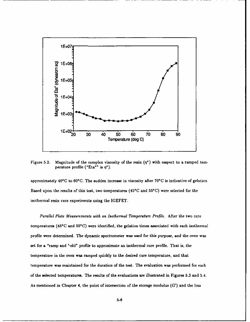
1 E+07
1E+06
1E+05
" 1E+04
1E+03
I E+02-20 30 40 50 60 70 80 90
Temperature (deg C)
Figure 5.2. Magnitude of the complex viscosity of the resin (,q*) with respect to a ramped tem-perature profile ("Eta*" is 77*).
approximately 400C to 600C. The sudden increase in viscosity after 700C is indicative of gelation.
Based upon the results of this test, two temperatures (450C and 550C) were selected for the
isothermal resin cure experiments using the IGEFET.
Parallel Plate Measurements with an Isothermal Temperature Profile. After the two cure
temperatures (45 0 C and 550C) were identified, the gelation times associated with each isothermal
profile were determined. The dynamic spectrometer was used for this purpose, and the oven was
set for a "ramp and ',old" profile to approximate an isothermal cure profile. That is, the
temperature in the oven was ramped quickly to the desired cure temperature, and that
temperature was maintained for the duration of the test. The evaluation was performed for each
of the selected temperatures. The results of the evaluations are illustrated in Figures 5.3 and 5.4.
As mentioned in Chapter 4, the point of intersection of the storage modulus (G') and the loss
5-6
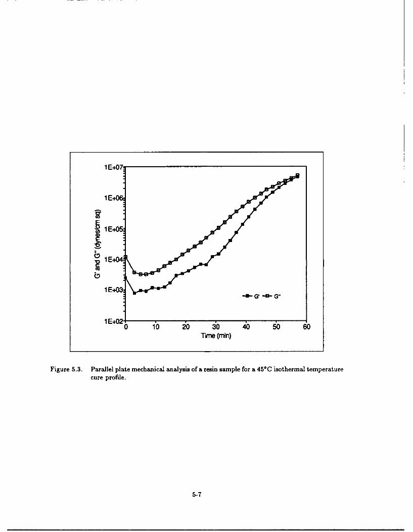
1 E+07
I E
1 1E+05
10+0
-- G -
0 10 i0 d0 4) 60lime (min)
Figure 5.3. Parallel plate mechanical analysis of a resin sample for a 45*C isothermal temperaturecure profile.
5-7
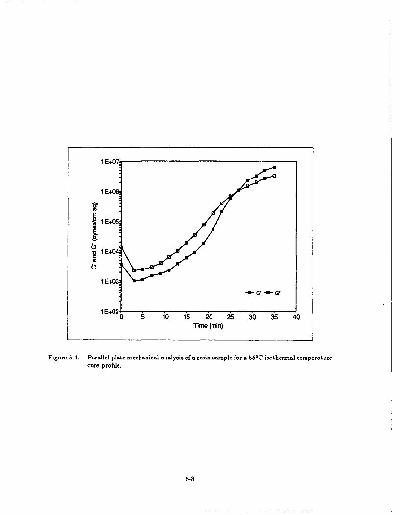
1 E+07
1 1E+05:
01 E+04:
1 E+e03,
G' -8 G-
I E+02I0 5 10 15 20 25 30 k3 40
Time (min)
Figure 5.4. Parallel plate mechanical analysis of a resin sample for a 550C isothermal temperaturecure profile.
5-8
modulus (G") can be used as an indicator of the resin's gelation point. From Figure 5.3, the point
of intersection for the 45"C profile occurs at approximately 60 minutes. (The evaluation was
terminated after 55 minutes because the capability of the equipment was exceeded at that point.
However, it is apparent from Figure 5.3 that the point of intersection of the two curves would
occur at approximately 60 minutes.) For the 55'C profile, the point of intersection occurred at
approximately 26 minutes into the cure, as illustrated in Figure 5.4. The reduction in the
viscosity (manifested by a corresponding reduction in G' and G") f:,r low cure times is typical of
curing resin systems (43). The same viscosity reduction is apparent in Figure 5.2. The effect is
e.-aggerated in Figdres 5.3 and 5.4 because the temperatures used in these evaluations were
ramped very quickly to the desired cure temperature. The temperature in Figure 5.2 was ramped
at a relatively slow rate (2"C per minute), and the corresponding viscosity reduction was more
gradual.
Torsional Bar Analysis of the Resin. Torsional bar analysis (TBA) was performed on resin
samples which were previously cured at 45"C and 55"C. As outlined in Chapter 4, the purpose of
TBA is to estimate the glass transition temperature of the material being tested. The results are
depicted in Figures 5.5 and 5.6. The glass transition temperature is typically reported as the
temperature which corresponds to the maximum value of the mechanical loss tangent (tan 6 ,)
(40:64). Analysis of the loss tangent curve in Figure 5.5 reveals that the glass transition
temperature for the sample cured at 45 0 C is approximately 80"C, which is well above the
sample's cure temperature. Analysis of the loss tangent curve for the sample cured at 55'C
(Figure 5.6) reveals that the glass transition temperature for this resin is approximately 70"C,
which is much closer to the sample's cure temperature.
5-9
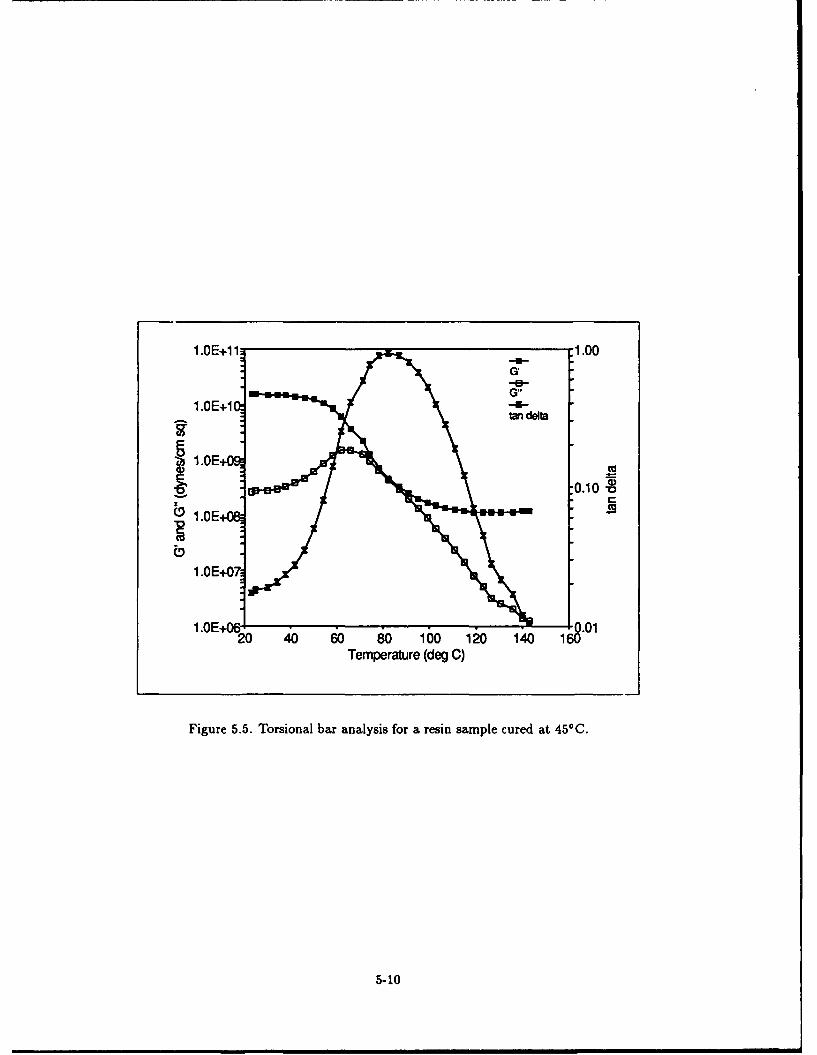
1.OE+1 1.00
1.OE+l -U-ton delta
t.OE
:0.10
S1.OE
1.OE+0
1.E 20 40 60 80 100 120 140 1-0Temperature (deg C)
Figure 5.5. Torsional bar analysis for a resin sample cured at 45 0C.
5-10
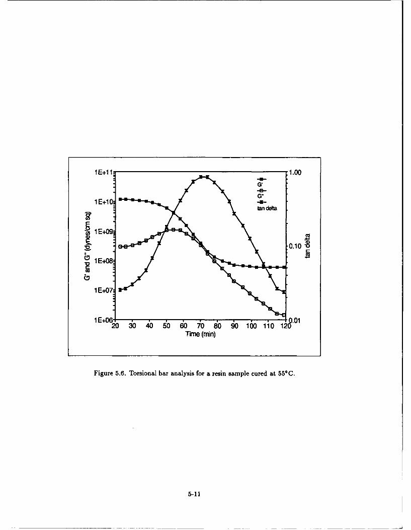
I E+1 1 1.00
1 E+1 a
I 1E+09
1 E+08
1 E+06700
20 30 40 50 60 70 80 90 100 110 120Thie (mihn)
Figure 5.6. Torsional bar analysis for a resin sample cured at 55*C.
5-11
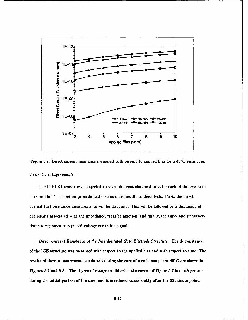
1 E+I12
1 1E+1 1
1E+10
1E+09
"_ 1 E+08 1 -M - 13rnin -5 25rain
- 37 min -m55 min -0I- 100 rin
1 E+07b 110
Applied Bias (volts)
Figure 5.7. Direct current resistance measured with respect to applied bias for a 450C resin cure.
Resin Cure Experiments
The IGEFET sensor was subjected to seven different electrical tests for each of the two resin
cure profiles. This section presents and discusses the results of these tests. First, the direct
current (dc) resistance measurements will be discussed. This will be followed by a discussion of
the results associated with the impedance, transfer function, and finally, the time- and frequency-
domain responses to a pulsed voltage excitation signal.
Direct Current Resistance of the Interdigitated Gate Electrode Structure. The dc resistance
of the IGE structure was measured with respect to the applied bias and with respect to time. The
results of these measurements conducted during the cure of a resin sample at 450C are shown in
Figures 5.7 and 5.8. The degree of change exhibited in the curves of Figure 5.7 is much greater
during the initial portion of the cure, and it is reduced considerably after the 55 minute point.
5-12
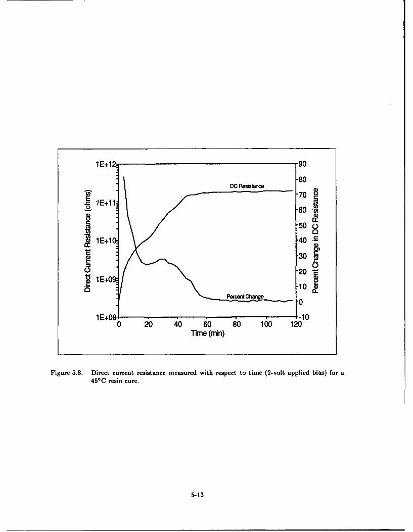
1 E+12 90
-80DC Resistance
-70.=IE+11-
500I 6050
-300))
10 (DPercent Chag
I E+O-100 20 40 g0 80 100 120
Time (min)
Figure 5.8. Direct current resistance measured with respect to time (2-volt applied bias) for a45*C resin cure.
5-1 3
This reduction in the rate of change is more effectively depicted in Figure 5.7. That is, the dc
resistance of the resin increases dramatically until approximately 55 minutes into the cure. At
this point, the rate of change is suddenly reduced. This behavior may be explained in terms of
the electrical conductivity mechanisms. DC resistance is a measure of the degree of loss in the
material. In an uncured resin, these losses are due primarily to ion transport. These ions are
present as unreacted components in the resin, or as byproducts of the resin's synthesis. As the
cure reaction progresses, more free ions are consumed in the cross-linking reaction, or they are
trapped in the cross-linked polymer, resulting in a conductance decrease, and hence, an increase
in the material's dc resistance. The point at which the dc resistance rate of change suddenly
decreases may be attributed to the onset of the resin's gelation. The dynamic mechanical tests
discussed in the previous section provided an estimate of the gelation time for a 450C cure of
approximately 60 minutes.
The results of the dc resistance measurements for a sample cured at 550C are given in
Figures 5.9 and 5.10. The trend noted in Figures 5.7 and 5.8 for a 450C cure are more difficult to
see in Figures 5.9 and 5.10. In Figure 5.9, in particular, it is difficult to see the decrease in the
rate of change of the dc resistance during the course of the cure. Figure 5.10 reveals that the dc
resistance of the IGE structure for a 550C cure did not increase above 2 Mg2. For the lower
temperature cure, however, the dc resistance increased to a point in excess of 100 Gfg. This
disparity between the results for the two cures is supported by other measurements, as well-most
notably the transfer function measurements and the impedance measurements. The obvious
conclusion is that there is a greater degree of electrical conduction in this sample compared to the
sample cured at 450 C. This may be due to the proximity of the sample's temperature to the glass
transition temperature. The temperature may be such that the material is not able to vitrify. If
this is the case, the material would remain in the rubbery state indefinitely, and its electrical
characteristics would not exhibit the same degree of change as observed with the lower cure
temperature.
5-14
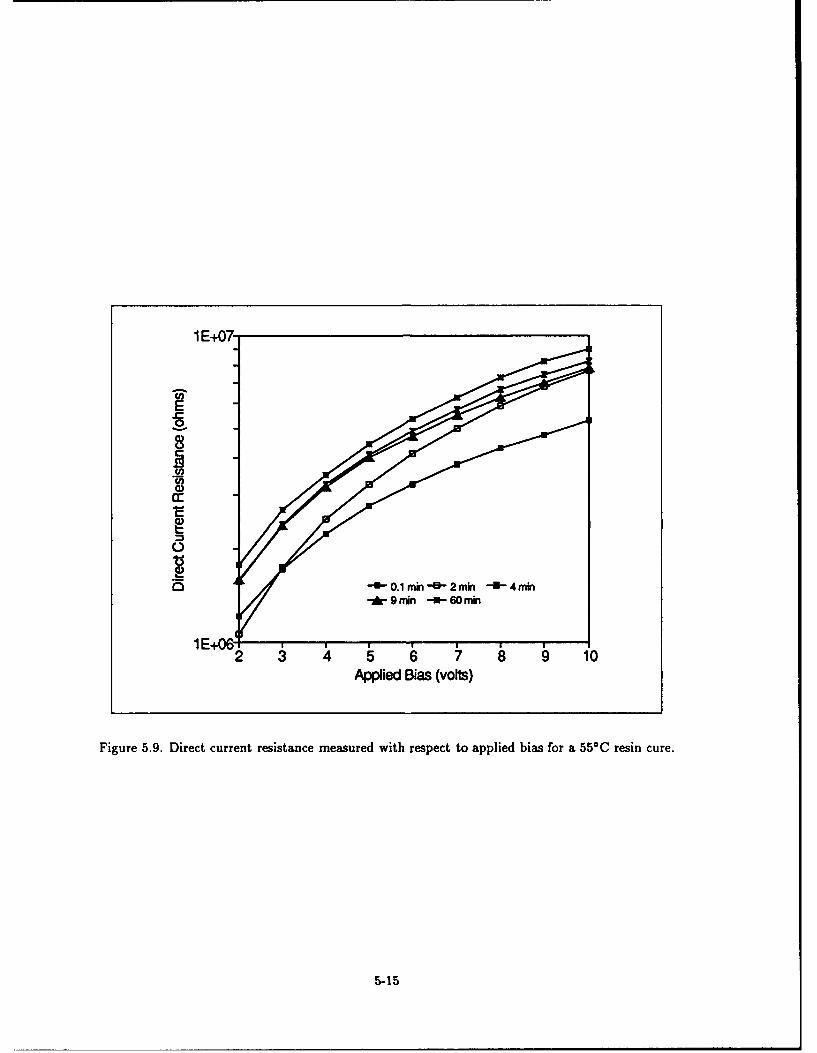
1 E+07-
E0
C
30 -60.lmm*-2min -4 4min-Ar 9mirn -U- 60min
2 3 4 i 8 9 1Applied Bias (voll)
Figure 5.9. Direct current resistance measured with respect to applied bias for a 5500 resin cure.
5-15
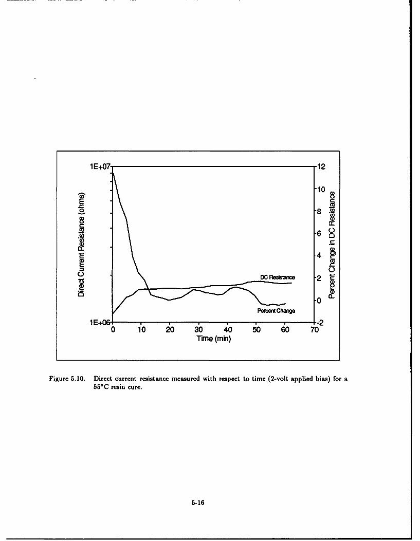
1 E+i07- 12
-10
E
.6
a: -
CC
0)Whag
0 10 20 i0 40 50 60 70Time (min)
Figure 5.10. Direct current resistance measured with respect to time (2-volt applied bias) for a550C resin cure.
5-16
Impedance of the Interdigitated Gate Electrode Structure. The impedance magnitude and
phase of the IGE structure were measured as discussed in Chapter 4. After the data was
collected, the real part and imaginary part of the impedance were extracted, and Cole-Cole plots
of the information were generated.
The impedance magnitude and phase for a sample of resin cured at 45*C are plotted in
Figures 5.11 through 5.14. These figures show that the impedance magnitude undergoes a
steady increase until approximately 60 minutes into the cure cycle. After 60 minutes, there is
relatively little change. Again, this is indicative of the onset of gelation in the resin (Figure 5.3).
The total current flow in the system is due to contributions from polarization mechanisms and
conduction mechanisms. Purely conductive behavior is indicated by a 0 degree phase angle, and
purely reactive behavior is indicated by a -90 degree phase angle. The phase information (Figure
5.13) indicates that, at the beginning of the cure process, conduction mechanisms dominate at
frequencies up to approximately 10 KHz. However, in the vicinity of 10 KHz, a transition in the
phase occurs which indicates a change in the dominant electrical transport mechanism from
conduction to that of polarization. Figure 5.14 indicates that after approximately ten minutes of
cure time, the polarization mechanisms dominate for frequencies above approximately 300 Hz.
After an hour there is very little change in the phase response of the resin.
There is also a well-defined notch in the magnitude of the impedance at approximately 400
Hz which appears after approximately 20 minutes into the cure (Figure 5.12). The notch is most
likely attributable to parasitic inductance introduced by the test equipment configuration, which
loads the IGE structure, in concert with phenomena at the electrode-resin interface, which will be
discussed in greater detail later in this chapter.
The impedance magnitude and phase measurement results for the 55*C cure are presented in
Figures 5.15 and 5.16. The trends noted in the 45*C cure are, in general, also present in this
information.
5-17
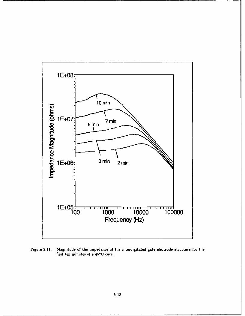
C
1 E-i.051 .. *u11~*I111
100 1'000 '10000, 100000Frequency (Hz)
Figure 5.11. Magnitude of the impedance of the interdigitated gate electrode structure for thefirst ten minutes of a 45*C cure.
5-18
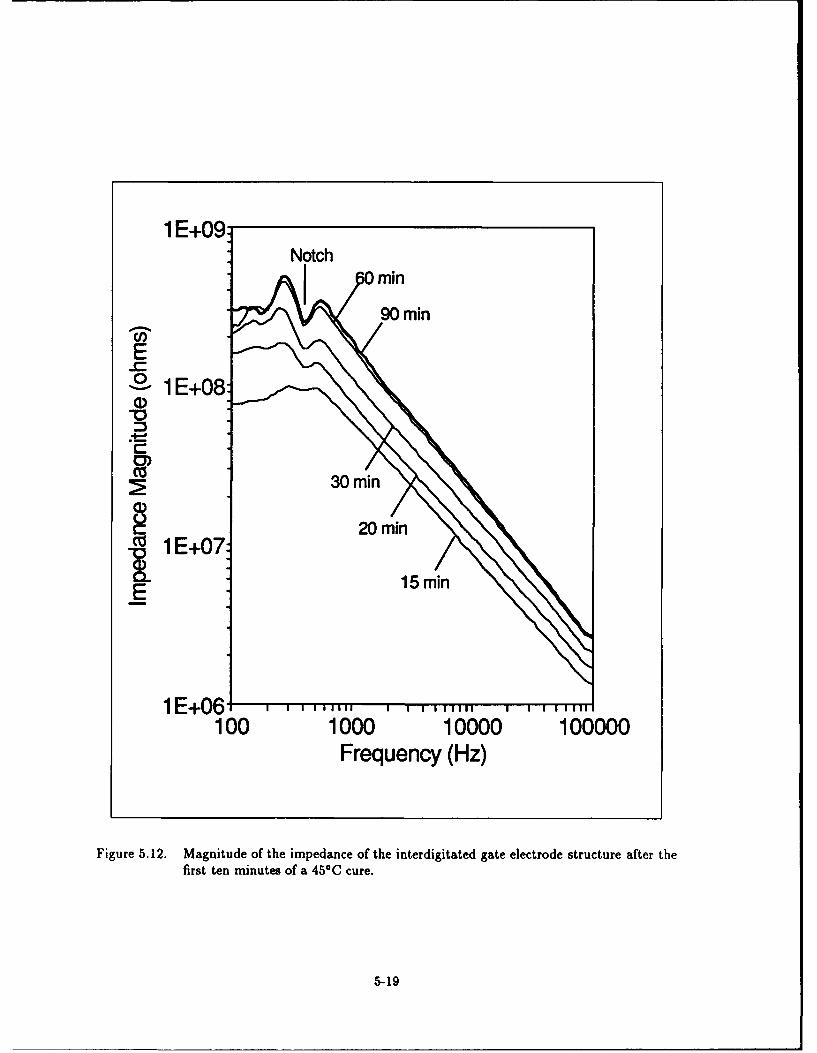
1 E+09:Notch
min90 min
C/
E
S1 E+081000
~30 min\
20 rain1 E+07
E 15 min
1 E+061 O0 1000 10000 100000
Frequency (Hz)
Figure 5.12. Magnitude of the impedance of the interdigitated gate electrode structure after thefirst ten minutes of a 45'C cure.
5-19
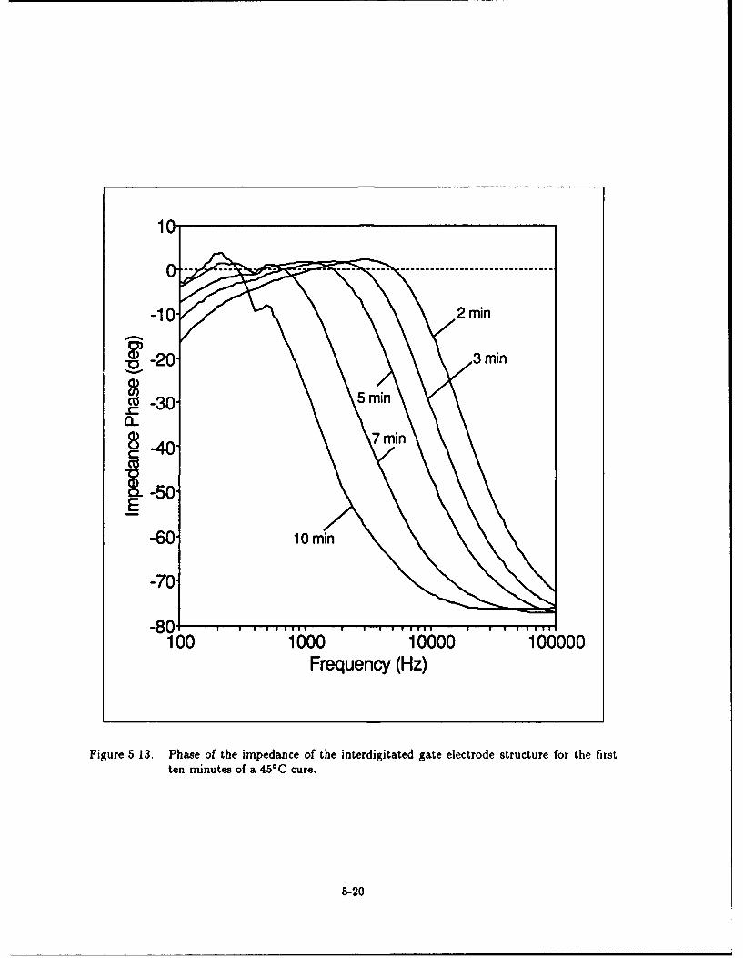
10-
ten- miue ofainCcue
-20- 3-mi
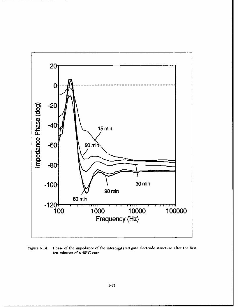
20-
~-20-
-40
~ -4015min
8 -60 20Omi
E -80-
-100-3mi90 min
60min-1201 1 1 111111 I 1 'I 111111100 1000 100 00000
Frequency (Hz)
Figure 5.14. Phase of the impedance of the interdigitated gate electrode structure after the firstten minutes of a 45*C cure.
5-21
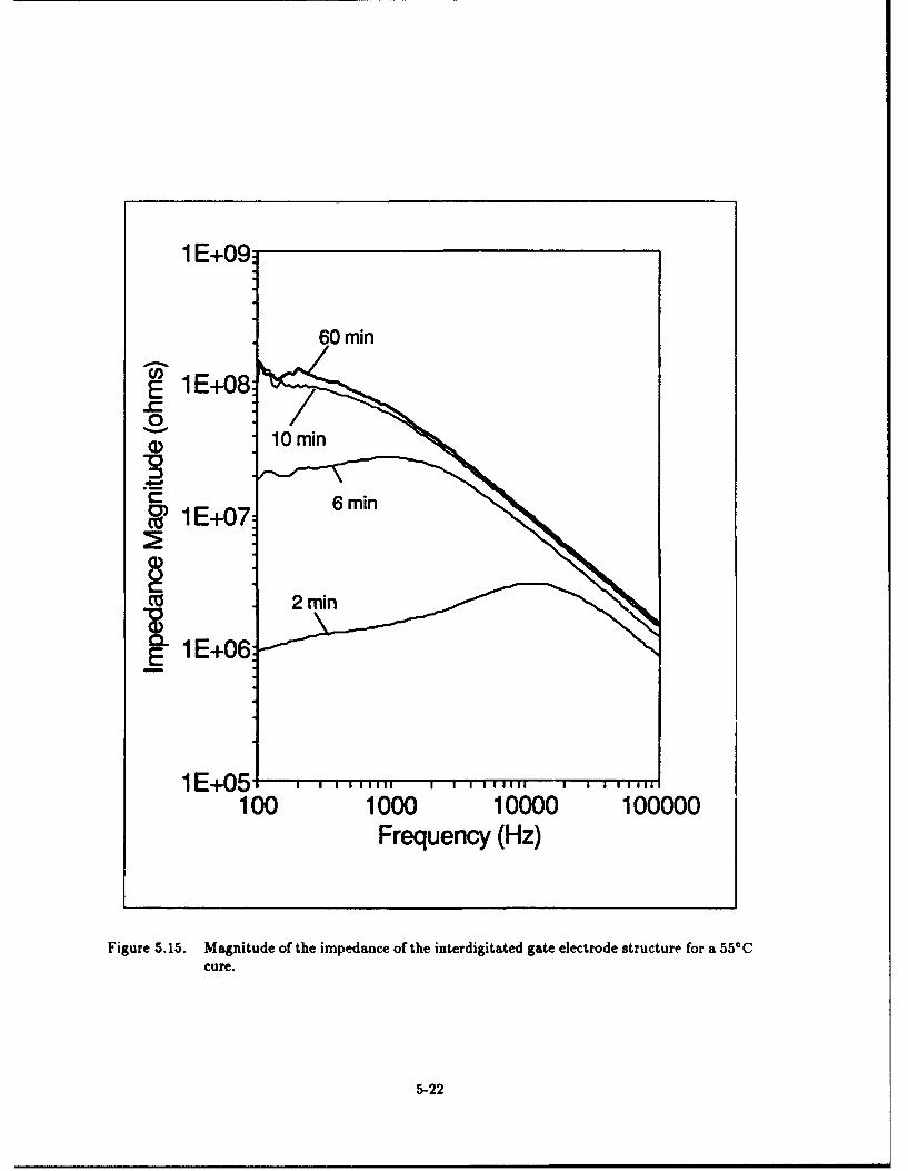
1 E+09
60 min
--
0 o 10 min
C6 min1 E+07:
IE 1 E+06: '
1 E+05, , ,,, ,, , , ,, ,, , , ,, ,,100 1000 10000 100000
Frequency (Hz)
Figure 5.15. Magnitude of the impedance of the interdigitated gate electrode structure for a 55 0 Ccure.
5-22
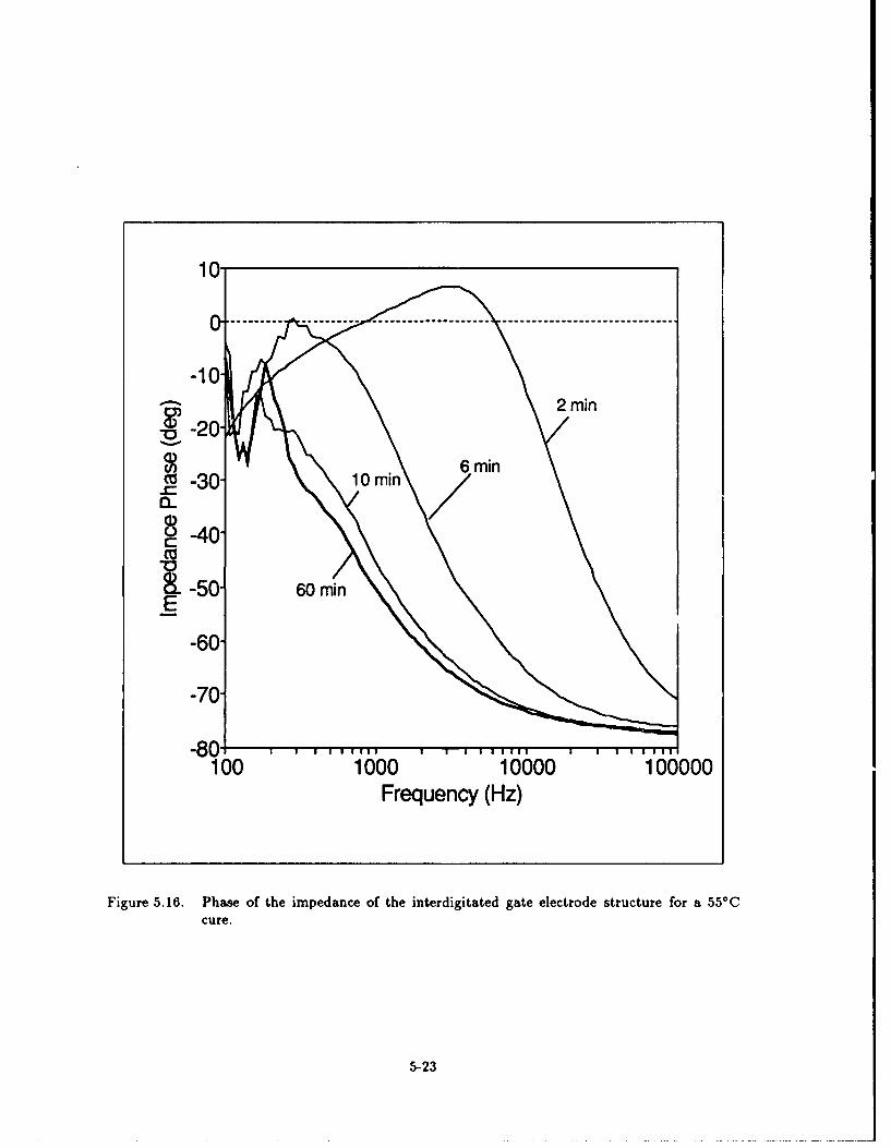
10-
-60
-70-
-8 111 z 11
100 1000001 00Frequency (Hz)
Figure 5.16. Phase of the impedance of the interdigitated gate electrode structure for a 55*Ccure.
5-23
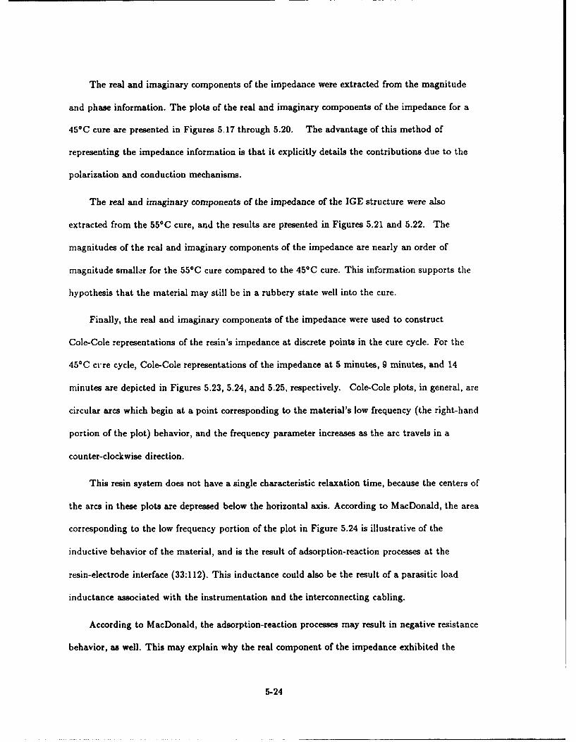
The real and imaginary components of the impedance were extracted from the magnitude
and phase information. The plots of the real and imaginary components of the impedance for a
45*C cure are presented in Figures 5.17 through 5.20. The advantage of this method of
representing the impedance information is that it explicitly details the contributions due to the
polarization and conduction mechanisms.
The real and imaginary components of the impedance of the IGE structure were also
extracted from the 55°C cure, and the results are presented in Figures 5.21 and 5.22. The
magnitudes of the real and imaginary components of the impedance are nearly an order of
magnitude smaller for the 55°C cure compared to the 45°C cure. This information supports the
hypothesis that the material may still be in a rubbery state well into the cure.
Finally, the real and imaginary components of the impedance were used to construct
Cole-Cole representations of the resin's impedance at discrete points in the cure cycle. For the
45°C ctre cycle, Cole-Cole representations of the impedance at 5 minutes, 9 minutes, and 14
minutes are depicted in Figures 5.23, 5.24, and 5.25, respectively. Cole-Cole plots, in general, are
circular arcs which begin at a point corresponding to the material's low frequency (the right-hand
portion of the plot) behavior, and the frequency parameter increases as the arc travels in a
counter-clockwise direction.
This resin system does not have a single characteristic relaxation time, because the centers of
the arcs in these plots are depressed below the horizontal axis. According to MacDonald, the area
corresponding to the low frequency portion of the plot in Figure 5.24 is illustrative of the
inductive behavior of the material, and is the result of adsorption-reaction processes at the
resin-electrode interface (33:112). This inductance could also be the result of a parasitic load
inductance associated with the instrumentation and the interconnecting cabling.
According to MacDonald, the adsorption-reaction processes may result in negative resistance
behavior, as well. This may explain why the real component of the impedance exhibited the
5-24
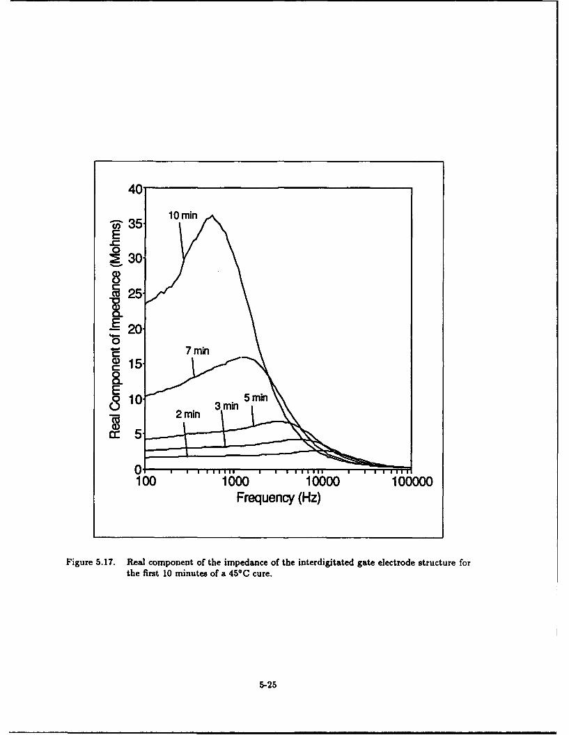
40'
- .O 35 10miE02-30•
.25
E 20"
7 min155 m
F)
E 101, 5 m rin
2 rain 3mi
100 1000 i0000 i60000Frequency (Hz)
Figure 5.17. Real component of the impedance of the interdigitated gate electrode structure forthe first 10 minutes of a 45C cure.
5-25
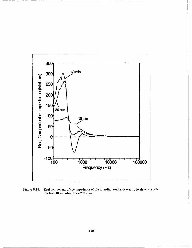
-~300 60min
E0 25a
~20a
2L150E9 30min
wZ100
CE
160 'iooo ioooo0 Y6000Frequency (Hz)
Figure 5.18. Real component of the impedance of the interdigitated gate electrode structure afterthe first 10 minutes of a 4500 cure.
5-26
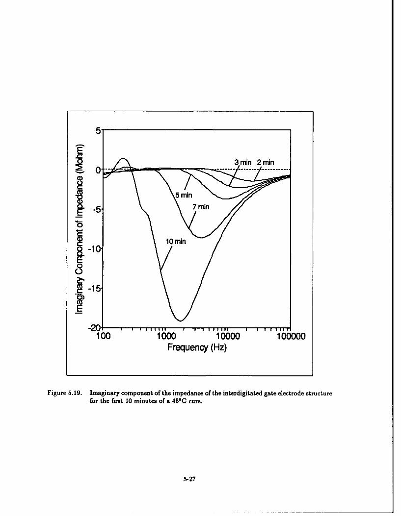
5
E.a
100mi
-152
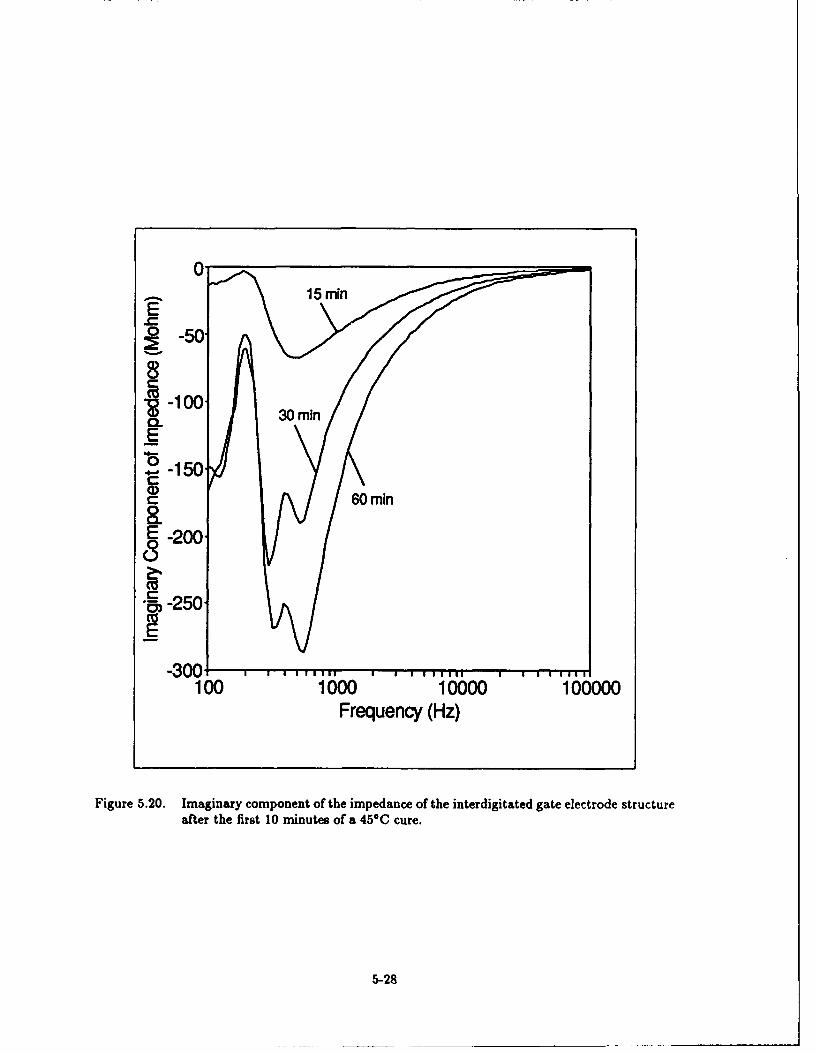
0.-~ 15min
0 -50-
-100 30minE
.- 150a ~60 min
8-
cm -250
-300 1 * 1 Iloilo. I I I I i ollU I I I I lol
100 1000 10000 100000Frequency (Hz)
Figure 5.20. Imaginary component of the impedance of the interdigitated gate electrode structureafter the first 10 minutes of a 45C cure.
5-28
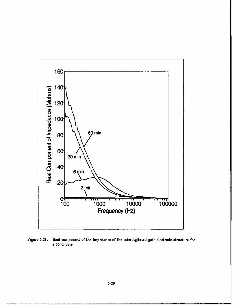
160"
S140"E0
S120"
~100-
E_ 0 6 min
60-
_.E 80 6mi mi
E
0- 60n
100 1000 10000 100000Frequency (Hz)
Figure 5.21. Real component of the impedance of the interdigitated gate electrode structure fora 55°C cure.
5-29
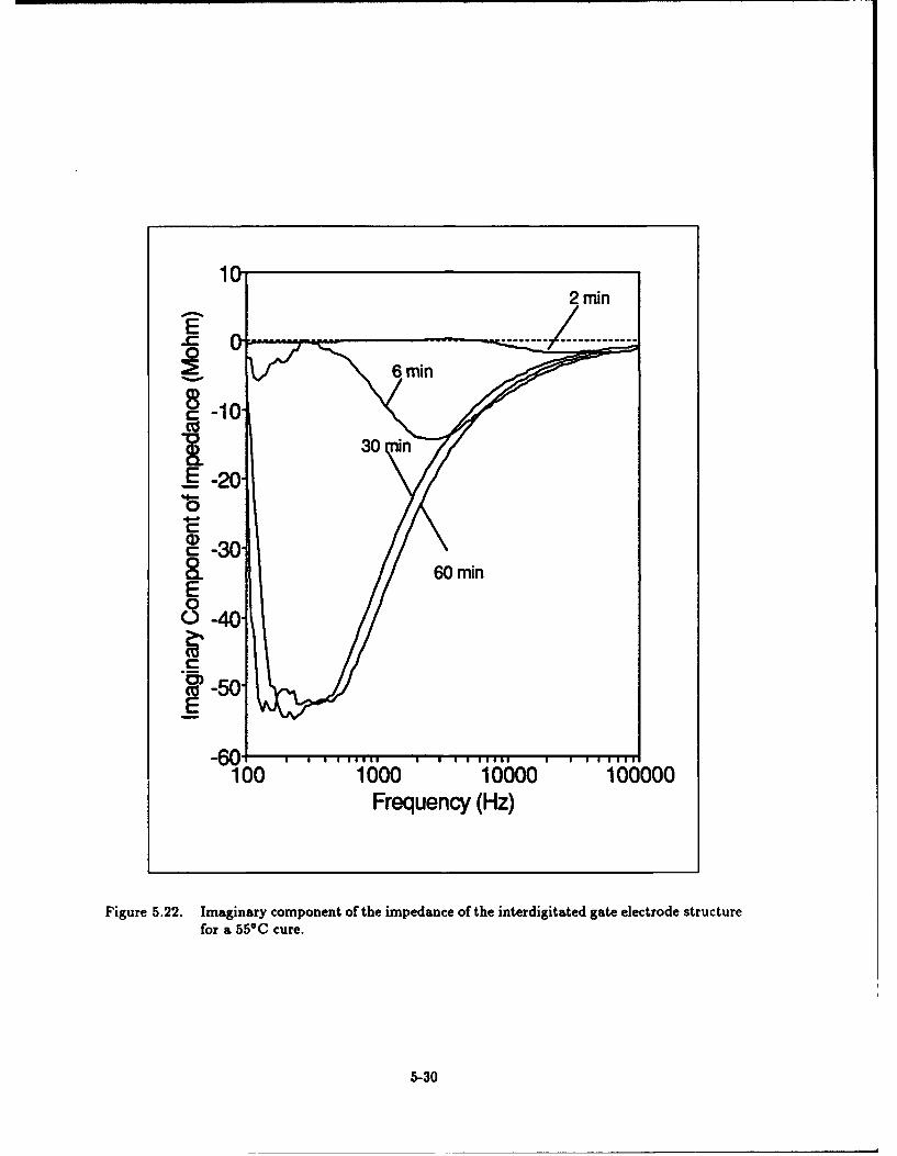
0
C
0
E
100 1000 10000 100000Frequency (Hz)
Figure 5.22. Imaginary component of the impedance of the interdigitated gate electrode structurefor a 55*C cure.
5-30
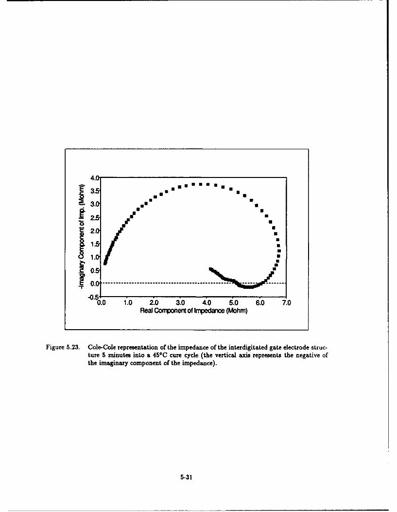
4.0
3.0
- 2.5 U U2.1.51.00.-""0.0 1".0 2.0 3.0 4.0 5.0 6.0 7.0
Real Component of Impedaroe (Mohm)
Figure 5.23. Cole-Cole representation of the impedance of the interdigitated gate electrode struc-ture 5 minutes into a 45°C cure cycle (the vertical axis represents the negative ofthe imaginary component of the impedance).
5-31
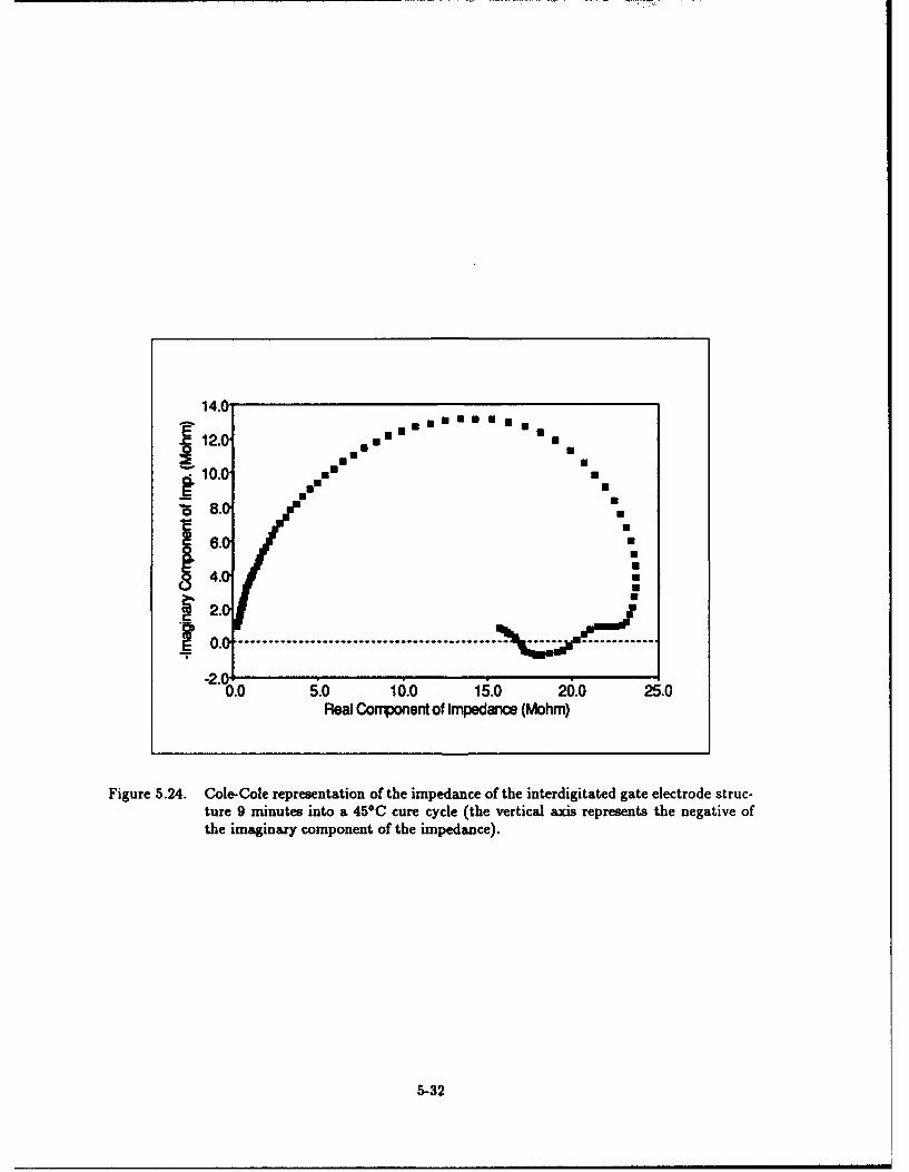
14.0-
fU= 12.0- MEN
.10.0 ME M
_ mmE Um
6.0 a
4.0
. 2.0o~o .................................. ..... ...........
02.0 --------------------------- Eff ie
-20.0.0 5.0 10.0 15.0 20.0 25.0
Real Component of Impedance (Mohm)
Figure 5.24. Cole-Cole representation of the impedance of the interdigitated gate electrode struc-ture 9 minutes into a 450C cure cycle (the vertical axis represents the negative ofthe imaginary component of the impedance).
5-32
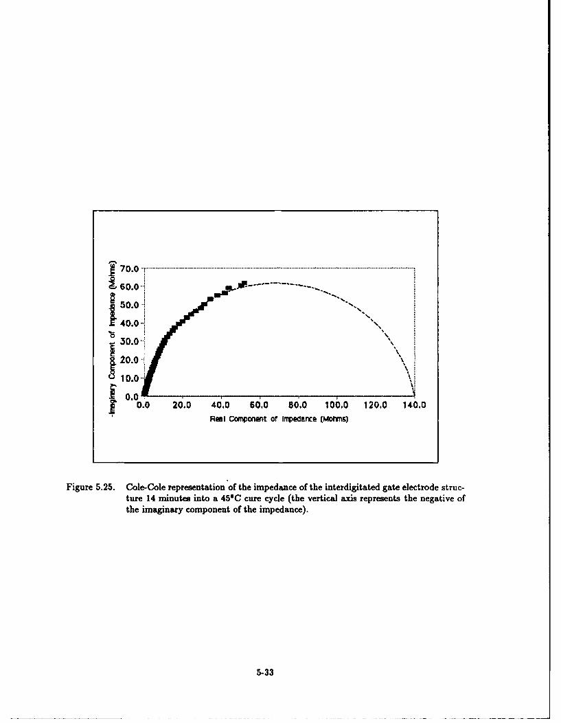
1 7 0 .0 .........................................................................................................................................................960.0-1
60. r, #----"-* .-- .. .
50.0
0.
.30.01
20.0
d10.0
0.00.0 20.0 40.0 60.0 80.0 100.0 120.0 140.0
Real Comnponent of linedarice (Morins)
Figure 5.25. Cole-Cole representation of the impedance of the interdigitated gate electrode struc-ture 14 minutes into a 450C cure cycle (the vertical axis represents the negative ofthe imaginary component of the impedance).
5-33
negative behavior for the 45C cure cycle at low frequencies (Figure 5.18). In Figure 5.25, the low
frequency magnitude of the impedance was such that the measurements were not reliable. That
is, given the specific instrument configuration utilized to measure the impedance of the IGE
structure, the impedance/gain-phase analyzer's upper limit of a reliabile measurement is
approximately 80 MO (determined empirically).
From these plots, the mean relaxation time (T'm) for the material can be estimated. It can be
discerned at the point where the imaginary component attains its maximum when W =nm - 1,
where wm is the frequency associated with this point (33:17). In Figure 5.24, the frequency at this
point (the apex of the curve) is approximately 16147.8 rad/sec. Solving the above relation for r,
yields a mean relaxation time for this system of approximately 62 psec. In contrast, a similar
measurement and calculation from the data in Figure 5.25 yields a mean relaxation time of
approximately 245 /sec. The relaxation time increase is due to the increase in the average size of
the molecules in the polymer, which makes it more difficult for the molecular dipoles to respond
to an electromagnetic stimulus.
Similar plots were constructed for the 550C cure. They are presented in Figures 5.26 through
5.29. This cure cycle produced significantly more well-behaved results because the impedance of
the material was not as large as was the case for the low temperature cure. The 2-minute
duration plot (Figure 5.26) exhibits the same characteristics as the short duration cure time plot
for the low temperature cure (Figure 5.23). Again, this behavior may be attributable to the
relatively high conductance of the material during the initial portion of the cure cycle. Utilizing
the expression =mrm - 1, the mean relaxation time, rm, can be calculated as discussed above.
The mean relaxation time for the plot corresponding to 10 minutes into the cure is approximately
162 psec. The mean relaxation time for the plots in Figures 5.28 and 5.29 are nearly the same,
approximately 231 psec.
5-34
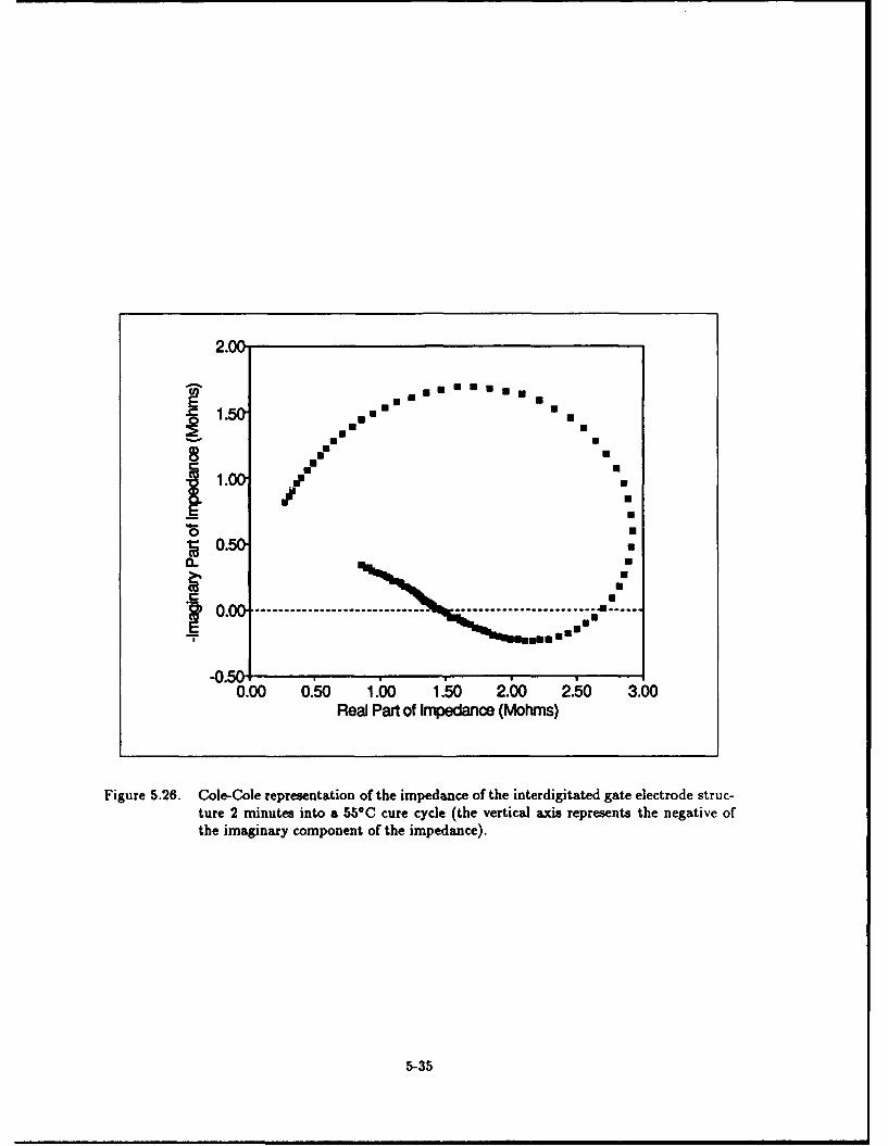
2.00-
E mM~ 1.5C ones
~1.00 o I?
10.5 U
-0.50U.-.
0.00 0.50 1.00 1.,50 2.00 2.50 3.00Real Part of Impedance (Mohms)
Figure 5.26. Cole-Cole representation of the impedance of the interdigitated gate electrode struc-ture 2 minutes into a 55*C cure cycle (the vertical axis represents the negative ofthe imaginary component of the impedance).
5-35
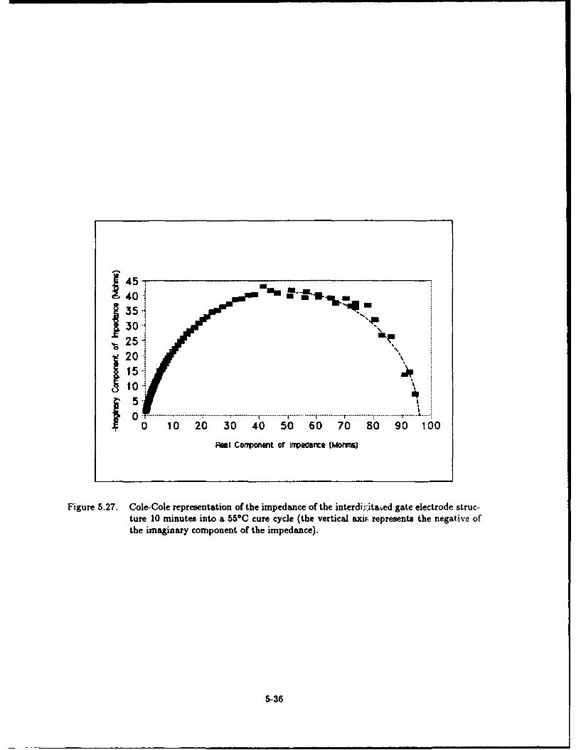
145 - -
401* u -
3250A
21
~10
0 .. ... ....................... ........i........... r........... ...
0 10 20 30 40 50 60 70 80 90 100
RNt Cowponmt of irripedarce wMorm~)
Figure 5.27. Cole-Cole representation of the impedance of the interdig-ita~ed gate electrode struc-ture 10 minutes into a 55*C cure cycle (the vertical axis represents the negative ofthe imaginary component of the impedance).
5-36
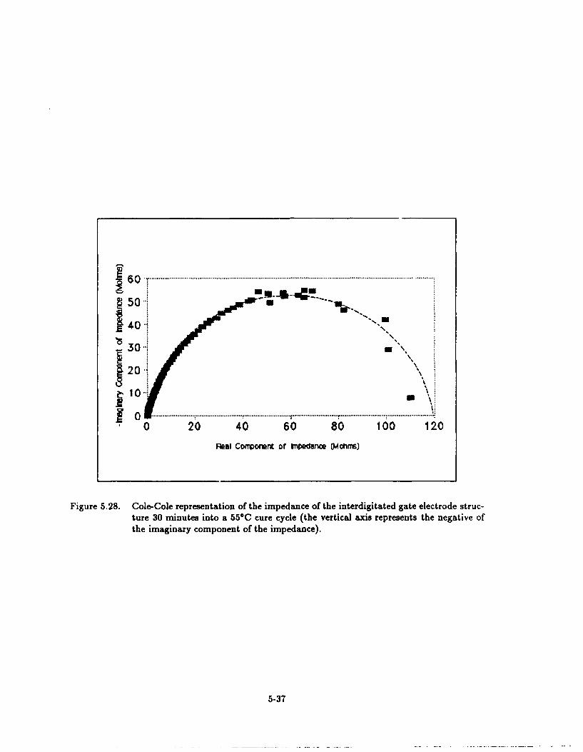
~50
.30'U
2 0
0 20 40 60 80 100 120
Real Conpont of IMdace (MoflrM)
Figure 5.28. Cole-Cole representation of the impedance of the interdigitated gate electrode struc-ture 30 minutes into a 55*C cure cycle (the vertical axis represents the negative ofthe imaginary component of the impedance).
5-37
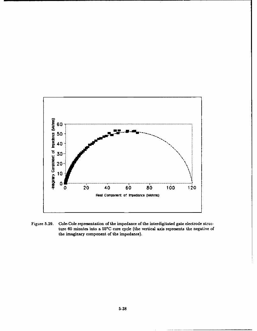
50 4
.40 -
R20
~10
. ........................... .........
0 20 40 60 80 100 120
Real Component of Impedance (Mohros)
Figure 5.29. Cole-Cole representation of the impedance of the interdigitated gate electrode struc-ture 60 minutes into a 5500 cure cycle (the vertical axis represents the negative ofthe imaginary component of the impedance).
5-38
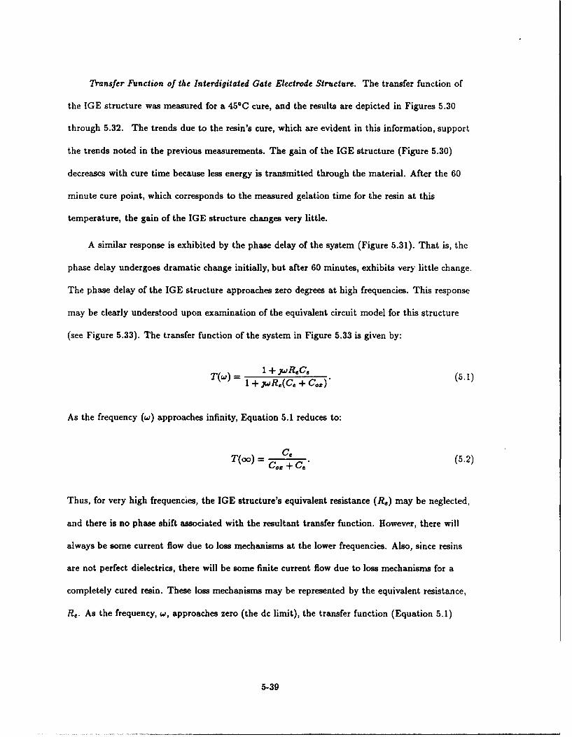
Transfer Function of the Interdigitated Gate Electrode Structure. The transfer function of
the IGE structure was measured for a 45*C cure, and the results are depicted in Figures 5.30
through 5.32. The trends due to the resin's cure, which are evident in this information, support
the trends noted in the previous measurements. The gain of the IGE structure (Figure 5.30)
decreases with cure time because less energy is transmitted through the material. After the 60
minute cure point, which corresponds to the measured gelation time for the resin at this
temperature, the gain of the IGE structure changes very little.
A similar response is exhibited by the phase delay of the system (Figure 5.31). That is, the
phase delay undergoes dramatic change initially, but after 60 minutes, exhibits very little change.
The phase delay of the IGE structure approaches zero degrees at high frequencies. This response
may be clearly understood upon examination of the equivalent circuit model for this structure
(see Figure 5.33). The transfer function of the system in Figure 5.33 is given by:
1 +JWReCeT(w) = 1 + jRn( C, + C o) (5.1)
As the frequency (w) approaches infinity, Equation 5.1 reduces to:
CeT(oo) = Co (5.2)
Thus, for very high frequencies, the IGE structure's equivalent resistance (R.) may be neglected,
and there is no phase shift associated with the resultant transfer function. However, there will
always be some current flow due to loss mechanisms at the lower frequencies. Also, since resins
are not perfect dielectrics, there will be some finite current flow due to loss mechanisms for a
completely cured resin. These loss mechanisms may be represented by the equivalent resistance,
R,. As the frequency, w, approaches zero (the dc limit), the transfer function (Equation 5.1)
5-39
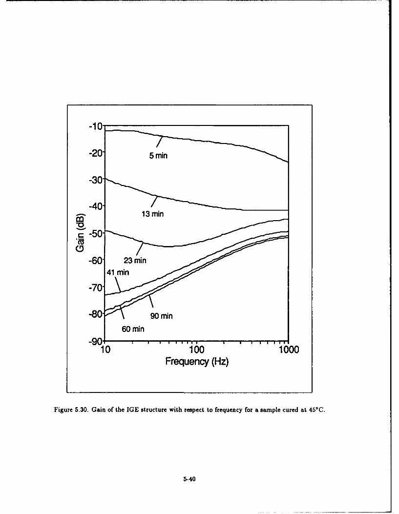
-10-20- i
-30-
-404~13 min
.-50"
0
-70-
-80-.-9 mi
-90- 60 ain
190 '''' 10 '~ '''' 1000
Frequency (Hz)
Figure 5.30. Gain of the IGE structure with respect to frequency for a sample cured at 45*C.
5-40
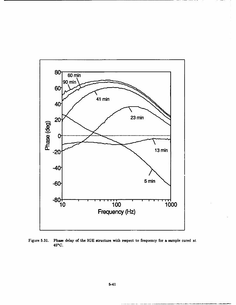
0
-4041
-10 60--- Gain -1- Phase
-20" 50
-30" 40
30-40"
rn "20
-10
-60"0
-70" "-10
-80" -20
-90 1 ' , , , , -300 10 20 30 40 50 60 70 8090 100
Time (min)
Figure 5.32. Gain and phase delay of the IGE structure with respect to time (frequency equal to10 Hz) for a sample cured at 450C.
5-42
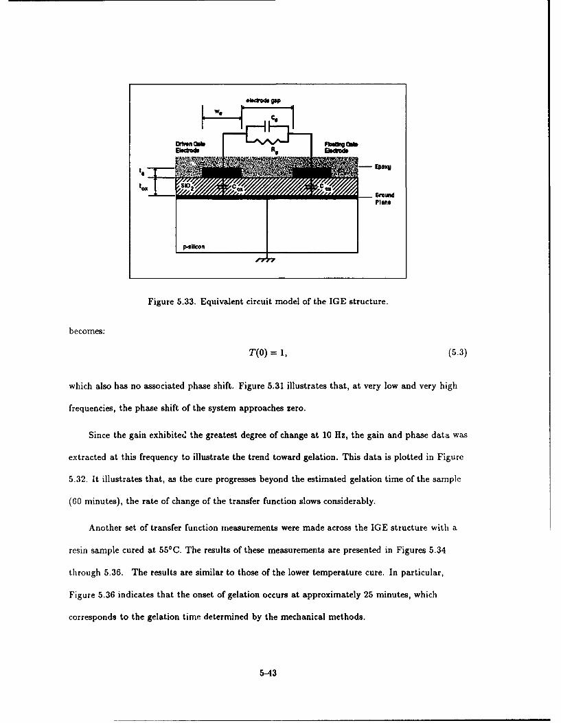
tDrken OabGa
p~silcon Plane
Figure 5.33. Equivalent circuit model of the IGE structure.
becomes:
T(O) = 1, (5.3)
which also has no associated phase shift. Figure 5.31 illustrates that, at very low and very high
frequencies, the phase shift of the system approaches zero.
Since the gain exhibited the greatest degree of change at 10 Hz, the gain and phase data was
extracted at this frequency to illustrate the trend toward gelation. This data is plotted in Figure
5.32. It illustrates that, as the cure progresses beyond the estimated gelation time of the sample
(60 minutes), the rate of change of the transfer function slows considerably.
Another set of transfer function measurements were made across the IGE structure with a
resin sample cured at 55°C. The results of these measurements are presented in Figures 5.34
through 5.36. The results are similar to those of the lower temperature cure. In particular,
Figure 5.36 indicates that the onset of gelation occurs at approximately 25 minutes, which
corresponds to the gelation time determined by the mechanical methods.
5-43
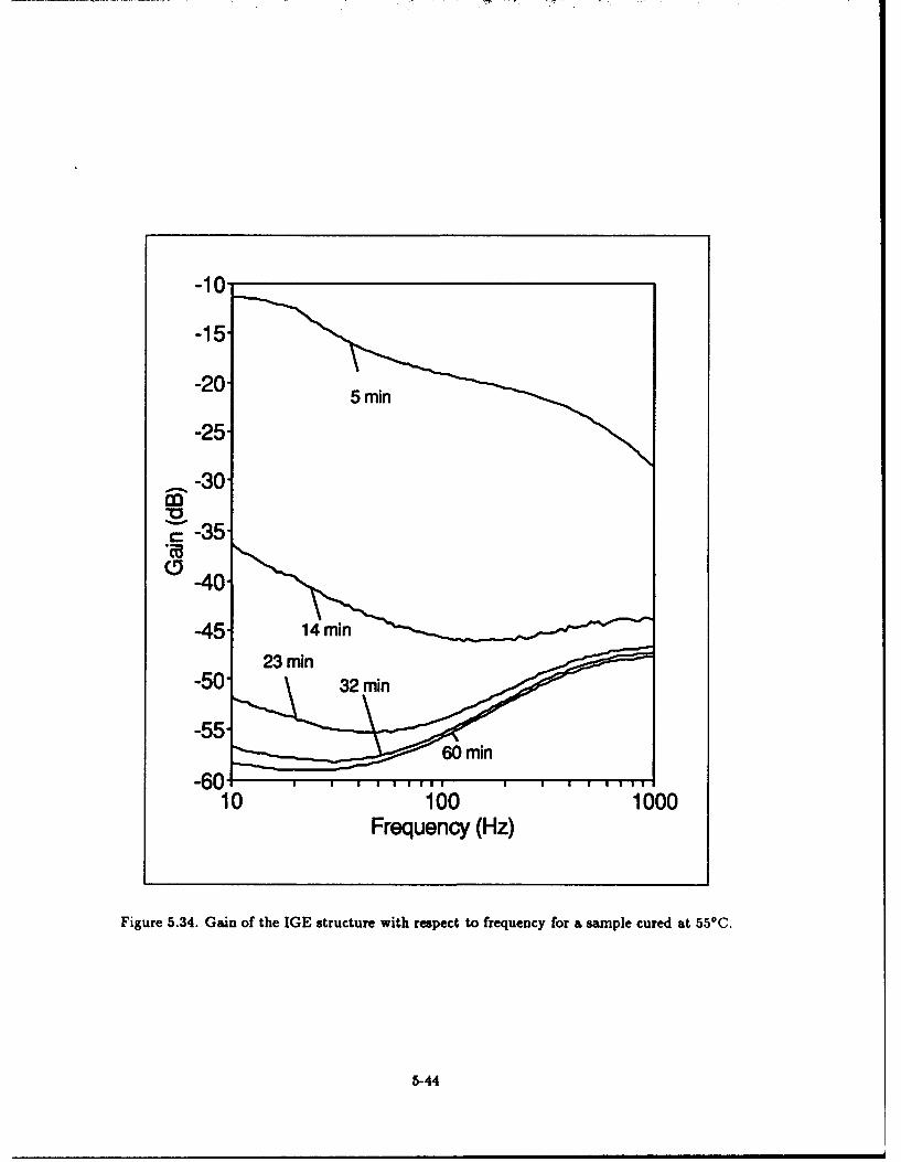
-10-
-15"
-20- i
-25
-30
60 10
0 -404
-45- 14 min
-5 23 min 3 i
-551
-60- 9 1 gill60 rain Igl
10 100 1000Frequency (Hz)
Figure 5.34. Gain of the IGE structure with respect to frequency for a sample cured at 55*C.
5-44
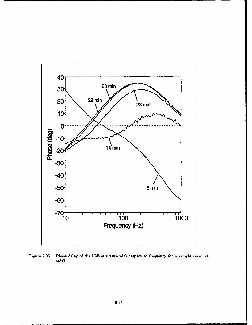
40
-50-
-60-
-70 2 I
10 100 1000 II
Frequency (Hz)
Figure 5.35. Phase delay of the IGE structure with respect to frequency for a sample cured at550C.
5-45
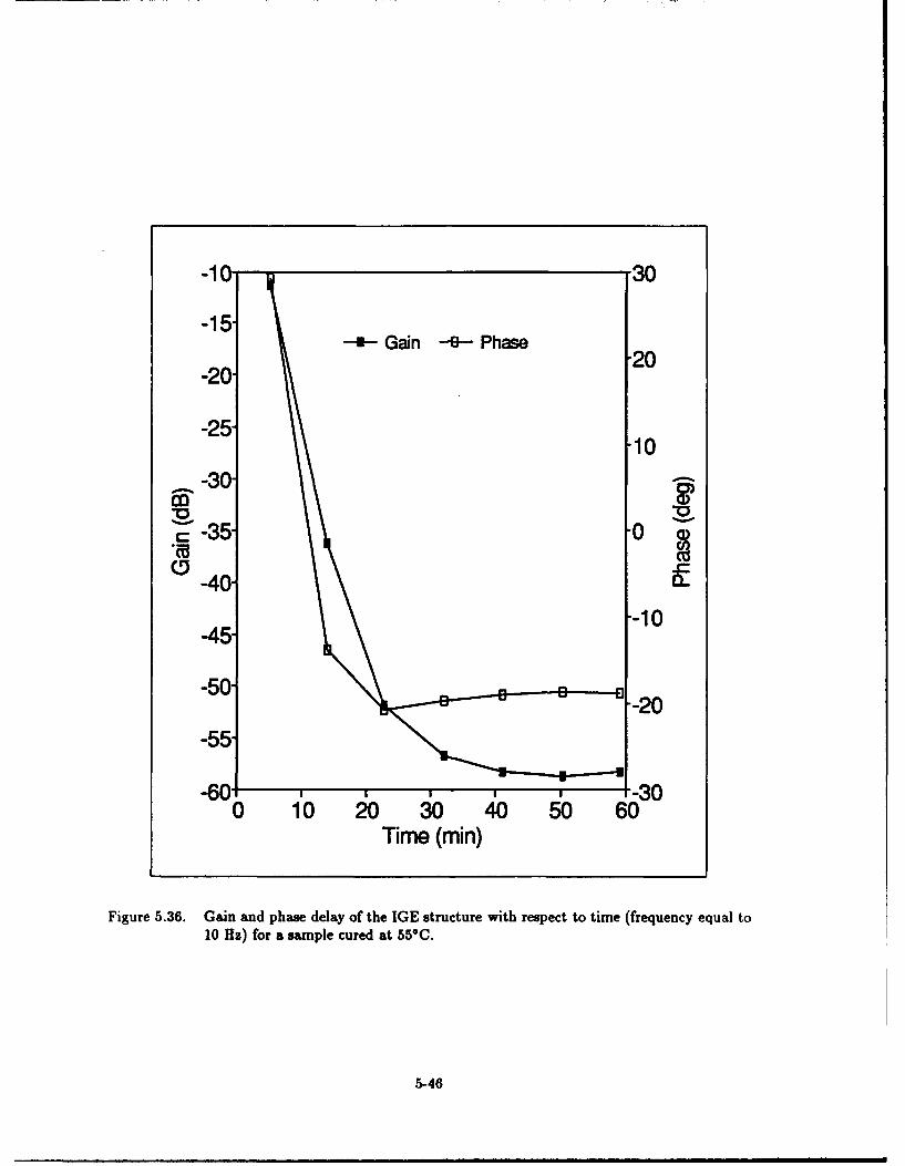
-10- 30
-15-SGain -- Ph~ase
-20- 20
-25-.10
-30-
~-35- 01
40--
-10-45-
-50-.-20
-55-
-60 30 10 20 30 40 50 60~
Time (min)
Figure 5.36. Gain and phase delay of the IGE structure with respect to time (frequency equal to10 Hz) for a sample cured at 55*C.
5-46
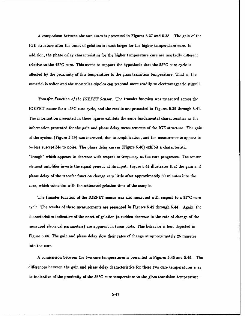
A comparison between the two cures is presented in Figures 5.37 and 5.38. The gain of the
IGE structure after the onset of gelation is much larger for the higher temperature cure. In
addition, the phase delay characteristics for the higher temperature cure are markedly different
relative to the 450C cure. This seems to support the hypothesis that the 55*C cure cycle is
affected by the proximity of this temperature to the glass transition temperature. That is, the
material is softer and the molecular dipoles can respond more readily to electromagnetic stimuli.
Transfer Function of the IGEFET Sensor. The transfer function was measured across the
IGEFET sensor for a 450C cure cycle, and the results are presented in Figures 5.39 through 5.41.
The information presented in these figures exhibits the same fundamental characteristics as the
information presented for the gain and phase delay measurements of the IGE structure. The gain
of the system (Figure 5.39) was increased, due to amplification, and the measurements appear to
be less susceptible to noise. The phase delay curves (Figure 5.40) exhibit a characteristi,
"trough" which appears to decrease with respect to frequency as the cure progresses. The sensor
element amplifier inverts the signal present at its input. Figure 5.41 illustrates that the gain and
phase delay of the transfer function change very little after approximately 60 minutes into the
cure, which coincides with the estimated gelation time of the sample.
The transfer function of the IGEFET sensor was also measured with respect to a 550C cure
cycle. The results of these measurements are presented in Figures 5.42 through 5.44. Again, the
characteristics indicative of the onset of gelation (a sudden decrease in the rate of change of the
measured electrical parameters) are apparent in these plots. This behavior is best depicted in
Figure 5.44. The gain and phase delay slow their rates of change at approximately 25 minutes
into the cure.
A comparison between the two cure temperatures is presented in Figures 5.45 and 5.46. The
differences between the gain and phase delay characteristics for these two cure temperatures may
be indicative of the proximity of the 550C cure temperature to the glass transition temperature.
5-47
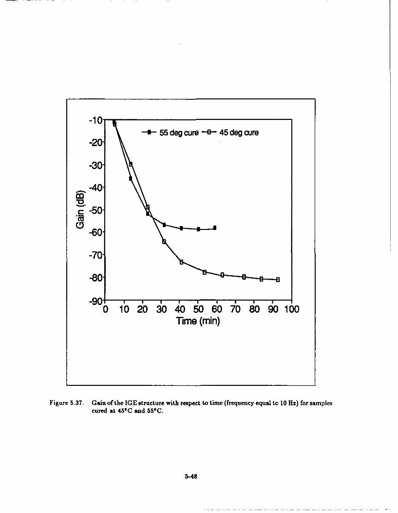
-10--- 55 deg curem B 45 deg cur
-20-
-30-
,--40-CO
c-50-
0 -60- -
-70
-80-
-90.0 10 2 0 4 0 60 7 0 6 6
Time (min)
Figure 5.37. Gain of the IGE structure with respect to time (frequency equal to 10 Hz) for samplescured at 450C and 55*C.
5-48
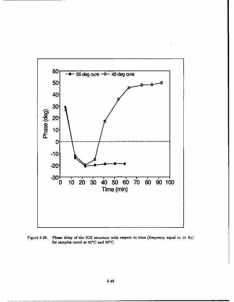
60 -- 55 deg cure-6B-45 deg cure
50-
40
3a
110-
-10-
-20-
-30-0 10 2030 40 5060 70 80 90 100
Time (min)
Figure 5.38. Phase delay of the IGE structure with respect to time (frequency equal to 10 llz)for samples cured at 45*C and 55*C.
5-49
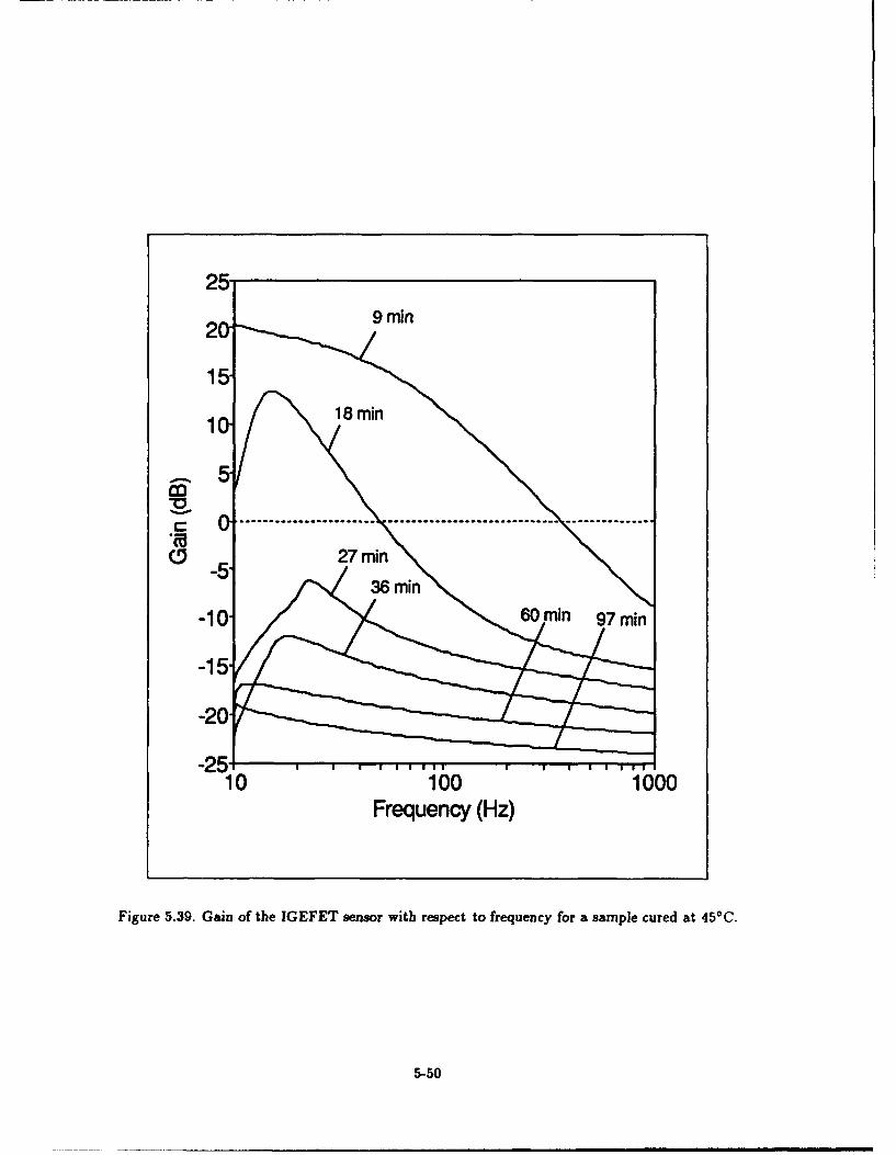
25-
29 9min
15-
1 a18min
-5C
-25.. . .. . .. .. .. .. . .. . .. . .. . ... .. . .. . .. .
-10 0mn 9 i
Frequency (Hz)
Figure 5.39. Gain of the IGEFET sensor with respect to frequency for a sample cured at 450 C.
5-50
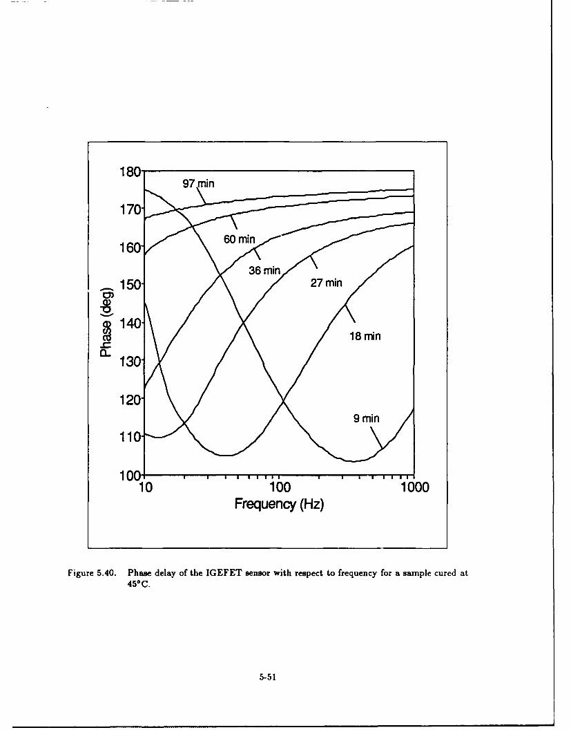
0-
170
Freque mncy(z
Figure ~ ~ ~ ~~ 3 5.0mhsiea o h GFTs nso ihrsett rqec o apecrda
150C27mi
140- 18-51
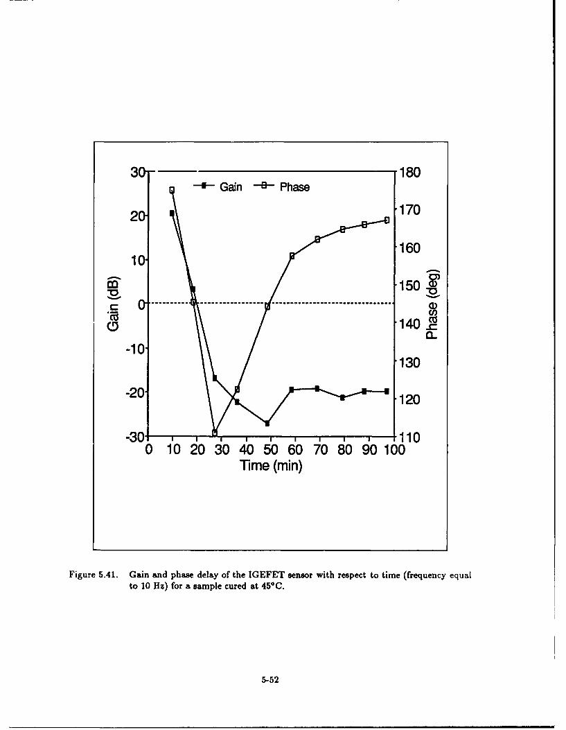
3a- 180-- Gain -6- Phase
2a 170
160
M -150 '
0 140.1-0a
-10.130
-20 120
-30- 1 1 1.1100 10 20 304050 6070 80 90100
Time (min)
Figure 5.41. Gain and phase delay of the IGEFET sensor with respect to time (frequency equalto 10 Hz) for a sample cured at 45*C.
5-52
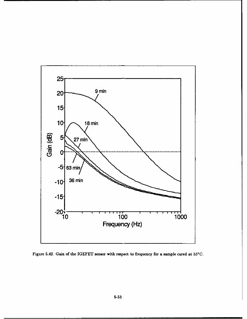
25-
2a9m
15-
1a 18min
v00 5. 27minC
-5- 63min
-10o 36min
-15-
-20'r I I I I I '
10 1010Frequency (Hz)
Figure 5.42. Gain of the IGEFET sensor with respect to frequency for a sample cured at 5500.
5-53
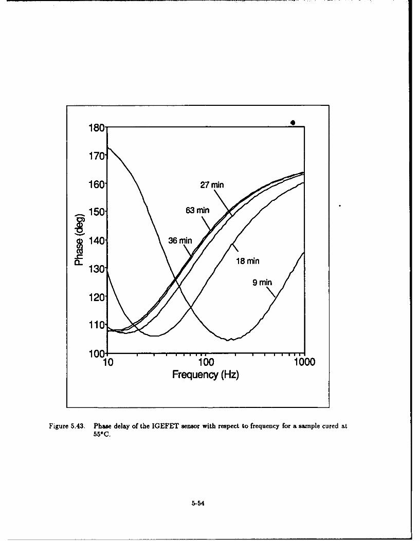
180-
170-
160-2mi
10 10000Frequency (Hz)
Figure 5.43. Phase delay of the IGEFET sensor with respect to frequency for a sample cured at550C.
5-54
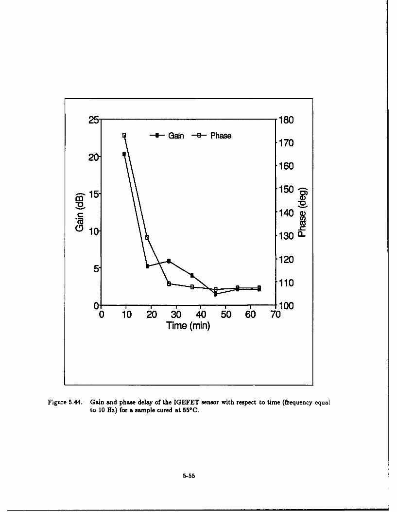
25 180"4- Gain -E-- Phase
1702a
160
-15 150-
.C 140
0130
1205
-110
0 , , , 1000 10 20 30 40 50 60 70
Time (min)
Figure 5.44. Gain and phase delay of the IGEFET sensor with respect to time (frequency equalto 10 Hz) for a sample cured at 55C.
5-55
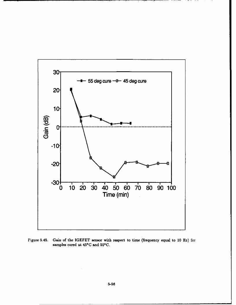
30,-- 55 deg cure -- 45 deg cure
2a
10
-20
-300 1O0 i30 40 4067 89060100
Time (min)
Figure 5.45. Gain of the IGEFET sensor with respect to time (frequency equal to 10 Hz) forsamples cured at 45*C and 550C.
5-56
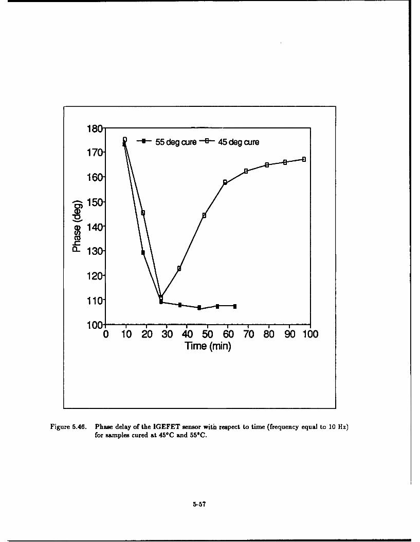
180--- 55 deg cure 6 45 degcuire
170-
160-
-150-
~140-CO
a-130-
120-
110.
100-0 10 2 0 4 0 60 7 0 9 6
Time (min)
Figure 5.46. Phase delay of the IGEFET sensor with respect to time (frequency equal to 10 Hz)for samples cured at 450C and 550C.
5-57
Time-Domain Response of the IGEFET Sensor to a Pulsed Voltage Ezcitation Signal. The
time-domain response of the IGEFET sensor to a pulsed voltage excitation signal was measured.
The pulse used was a 3-volt, 5-psec wide, 10 KHz repetitive frequency pulse. The reasons for
choosing this signal were twofold. First, it was necessary to use a signal with sufficient energy.
That is, the width and height of the pulse were selected such that the output response signal was
measurable and well-behaved throughout the cure cycle. Second, in order to effectively dissipate
the energy supplied by the excitation signal, it was necessary to use a period that was large
compared to the pulse's width. The pulse's amplitude needed to be less than 5 volts to prevent
exceeding the bias levels of the SE amplifier transistors. The 3-volt level was selected arbitrarily.
The pulse's width was established experimentally. A resin sample was cured. During the cure
cycle, the width of the pulse was varied. It was determined that in relation to a 10 KHz repetition
frequency, a 5-pusec wide pulse contained enough information, and allowed the IGE-resin system
to dissipate the energy prior to the application of a subsequent pulse. The excitation pulse is
depicted in Figure 5.47. The results of the measurements for a 45*C cure are illustrated in
Figures 5.48 and 5.49. The non-linear initial response of the sensor (the 5 minute contour in
Figure 5.48) indicates that a significant amount of energy was not dissipated before the pulse was
re-applied. This behavior changed within the first 10 minutes of the cure cycle. A gradual
decrease in the amplitude of the output signal is illustrated in Figure 5.49, until, after 60 minutes,
relatively little change in the amplitude occurs. This behavior is consistent with the estimated
gelation point of the resin.
The time-domain response of the IGEFET sensor to a pulsed voltage excitation for a 55*C
cure cycle is illustrated in Figure 5.50. The resin cured at this temperature exhibited a non-linear
response during its initial cure times, as well. The system also exhibited a dramatic decrease in
the rate of change of the amplitude in the vicinity of the estimated cure time.
5-58
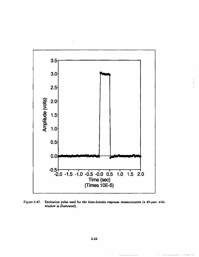
3.5
3.0-
2.5-
"2.0-
S1.5-
E 1.0-
0.5-
0.0 .
-0.5 1 1-2.0 -1.5 -1.0 -0.5 -0.0 0.5 1.0 1.5 2.0
Time (sec)(Times 1 OE-5)
Figure 5.47. Excitation pulse used for the time-domain response measurements (a 40-/usec widewindow is illustrated).
5-59
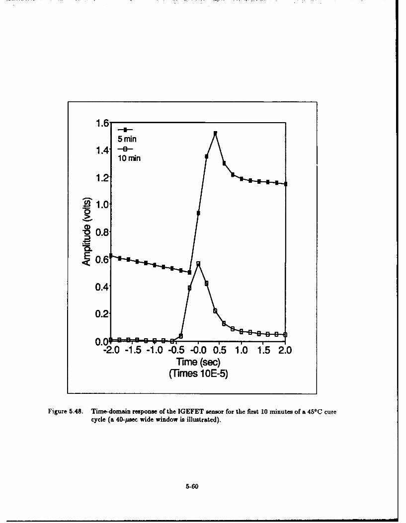
1.65 min
1.4 --8-10 min
1.2
A 1.o
-8 0.8'0.
0.4
0.011-2.0 -1.5 -1.0 -0.5 -0.0 0.5 1.0 1.5 2.0
Time (sec)(Times 1 0E-5)
Figure 5.48. Time-domain response of the IGEFET sensor for the first 10 minutes of a 450C curecycle (a 40-psec wide window is illustrated).
5-60
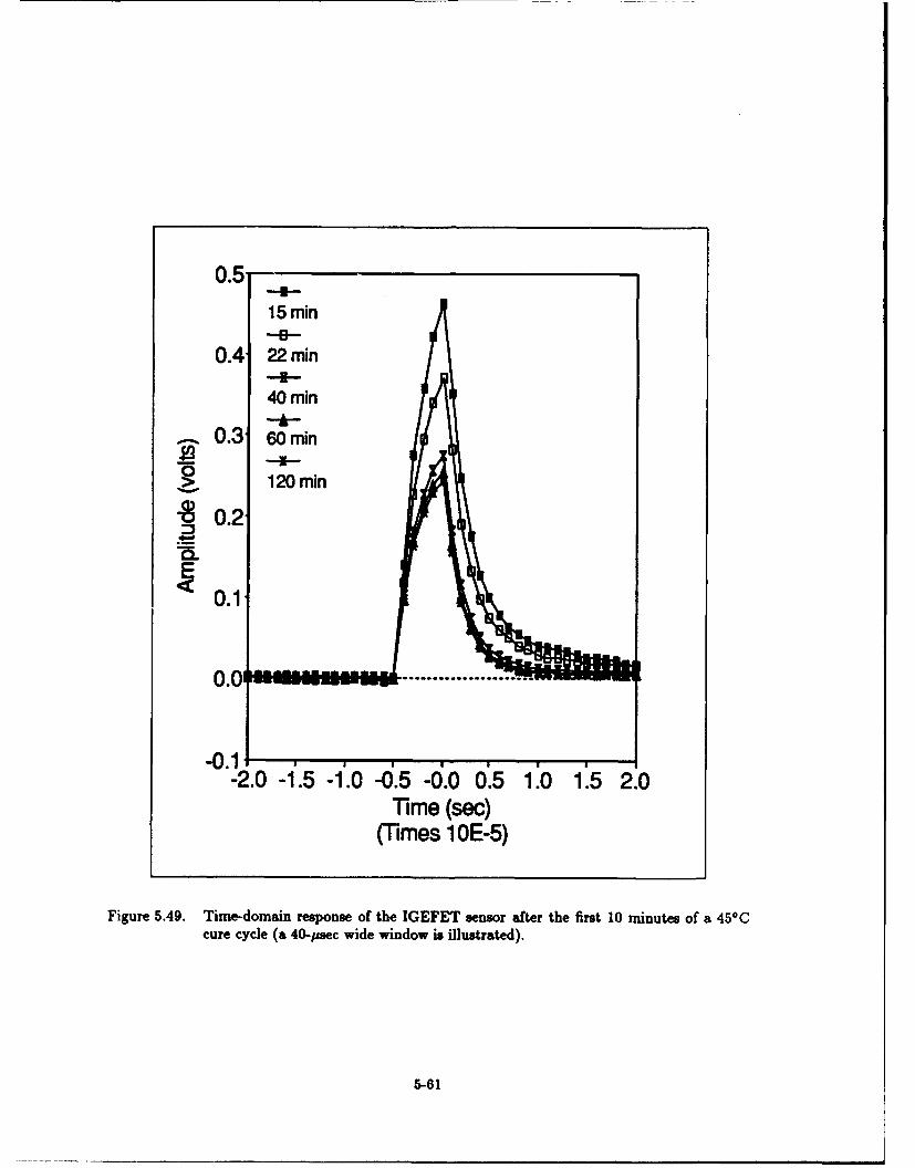
0.5
15 min-8-
0.4 22 min
40 min
0.3 60 min
0 120 min
~0.2
0.1
0.0 - -...........
-0.1 ,-2.0 -1.5 -1.0 -0.5 -0.0 0.5 1.0 1.5 2.0
Time (sec)(Times 1 OE-5)
Figure 5.49. Time-domain response of the IGEFET sensor after the first 10 minutes of a 45°Ccure cycle (a 40-psec wide window is illustrated).
5-61
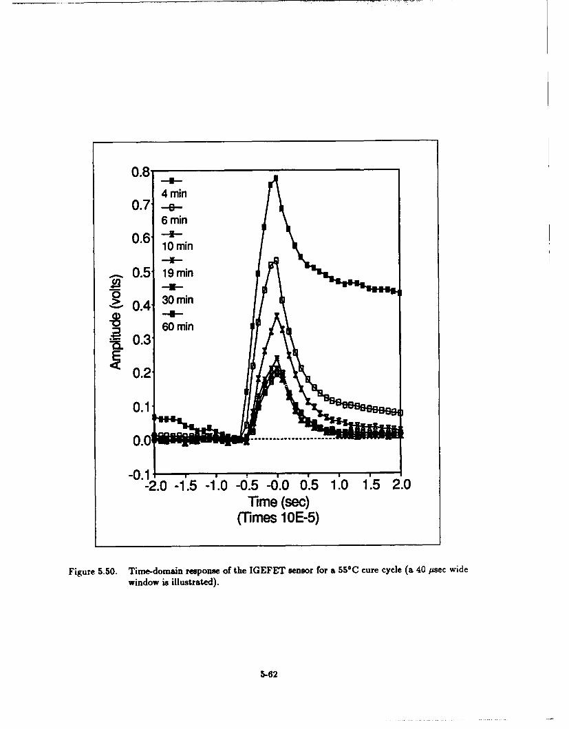
0.8-4 min
0.7- ---6 min
0.6-~10min
0I
0.519 i
-2.0 -15-.m0.i00 05n. . .
lime (sc
(Times 1OE-5)
Figure 5.50. Time-domain response of the IGEFET sensor for a 55*C cure cycle (a 40,usec widewindow is illustrated).
5-62
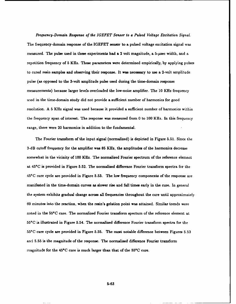
Frequency-Domain Response of the IGEFET Sensor to a Pulsed Voltage Excitation Signal.
The frequency-domain response of the IGEFET sensor to a pulsed voltage excitation signal was
measured. The pulse used in these experiments had a 2 volt magnitude, a 5-psec width, and a
repetition frequency of 5 KHz. These parameters were determined empirically, by applying pulses
to cured resin samples and observing their response. It was necessary to use a 2-volt amplitude
pulse (as opposed to the 3-volt amplitude pulse used during the time-domain response
measurements) because larger levels overloaded the low-noise amplifier. The 10 KHz frequency
ured in the time-domain study did not provide a sufficient number of harmonics for good
resolution. A 5 KHz signal was used because it provided a sufficient number of harmonics within
the frequency span of interest. The response was measured from 0 to 100 KHz. In this frequency
range, there were 20 harmonics in addition to the fundamental.
The Fourier transform of the input signal (normalized) is depicted in Figure 5.51. Since the
3-dB cutoff frequency for the amplifier was 85 KHz, the amplitudes of the harmonics decrease
somewhat in the vicinity of 100 KHz. The normalized Fourier spectrum of the reference element
at 45*C is provided in Figure 5.52. The normalized difference Fourier transform spectra for the
45*C cure cycle are provided in Figure 5.53. The low frequency components of the response are
manifested in the time-domain curves as slower rise and fall times early in the cure. In general
the system exhibits gradual change across all frequencies throughout the cure until approximately
60 minutes into the reaction, when the resin's gelation point was attained. Similar trends were
noted in the 55*C cure. The normalized Fourier transform spectum of the reference element at
55*C is illustrated in Figure 5.54. The normalized difference Fourier transform spectra for the
55*C cure cycle are provided in Figure 5.55. The most notable difference between Figures 5.53
and 5.55 is the magnitude of the response. The normalized difference Fourier transform
magnitude for the 45*C cure is much larger than that of the 55*C cure.
5-63
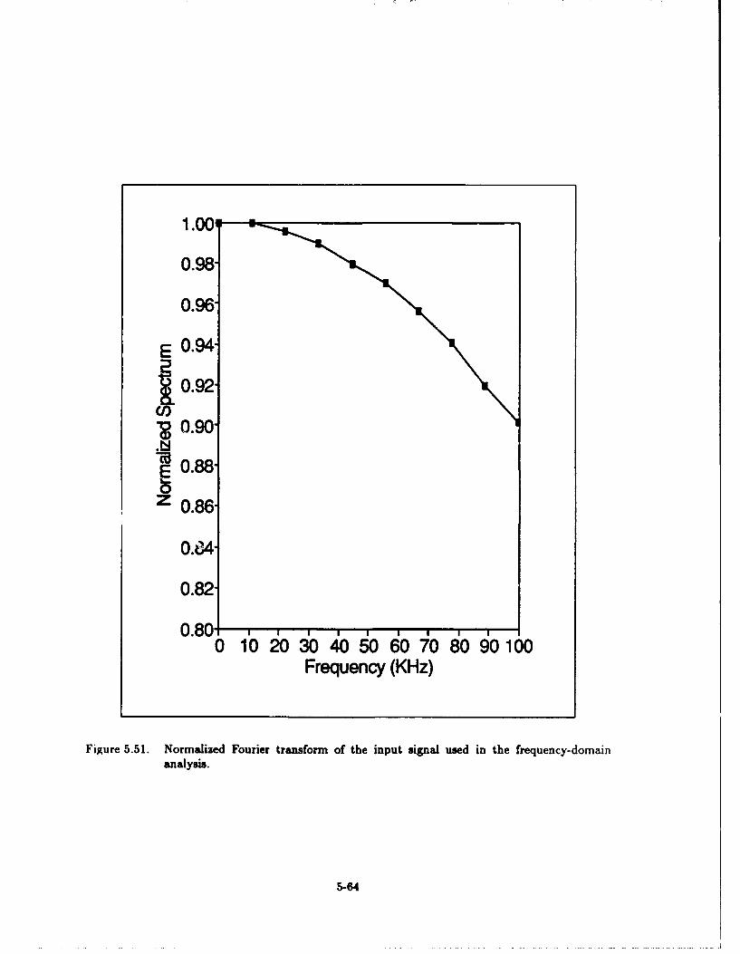
1.00:
0.98-
0.96
E 0.94-
2.0.92"
C,,o.90.
._ 0.86-0.88-
Z 0.86 o
0.82-
0.800 20 30 40 50 dO O 80 90 100
Frequency (KHz)
Figure 5.51. Normalized Fourier transform of the input signal used in the frequency-domainanalysis.
5-64
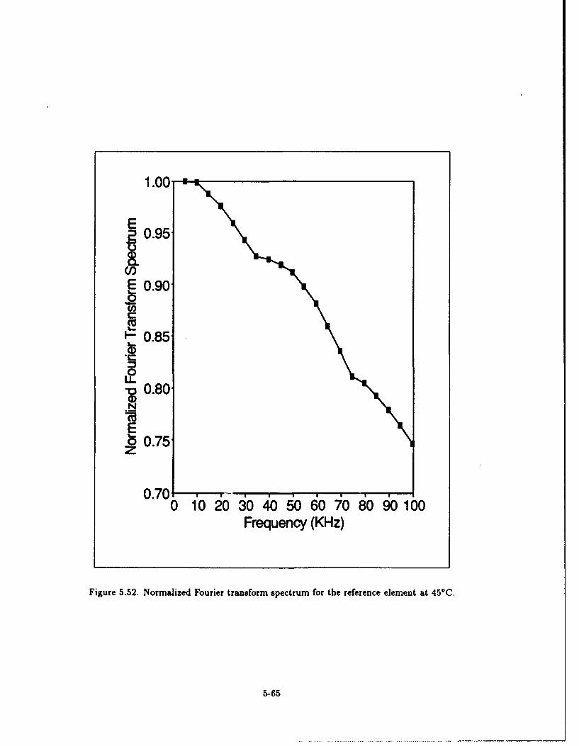
1.00.
E 0.90
c% 0.85-
-~0.80-
60.75-
0.701 -r-r0 1020 3040 50 6070 8090 100
Frequency (KHz)
Figure 5.52. Normalized Fourier transform spectrum for the reference element at 450 C.
5-65
0.40-
0.35- E3-
E0.30- 25 min
47 minE 0.25-
-. 0- 68 minC HF
0.20- 120 min
o 0.15-
,D 0.10-a)
0.05-
0.000 10 2030 4050 6070 80 90100
Frequency (KHz)
Figure 5.53. Normalized difference Fourier transform magnitude spectra for a 45*C cure.
5-66
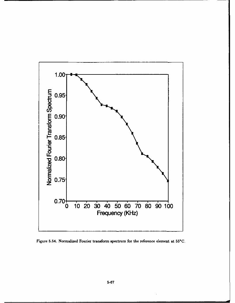
1.00 "
I 0.95"
E 0.90"10
F- 0.85-
. 0.80"N
o 0.75-
0.7011'0 0 0 4b 90 60 70 80 60 100
Frequency (KHz)
Figure 5.54. Normalized Fourier transform spectrum for the reference element at 550C.
5-67
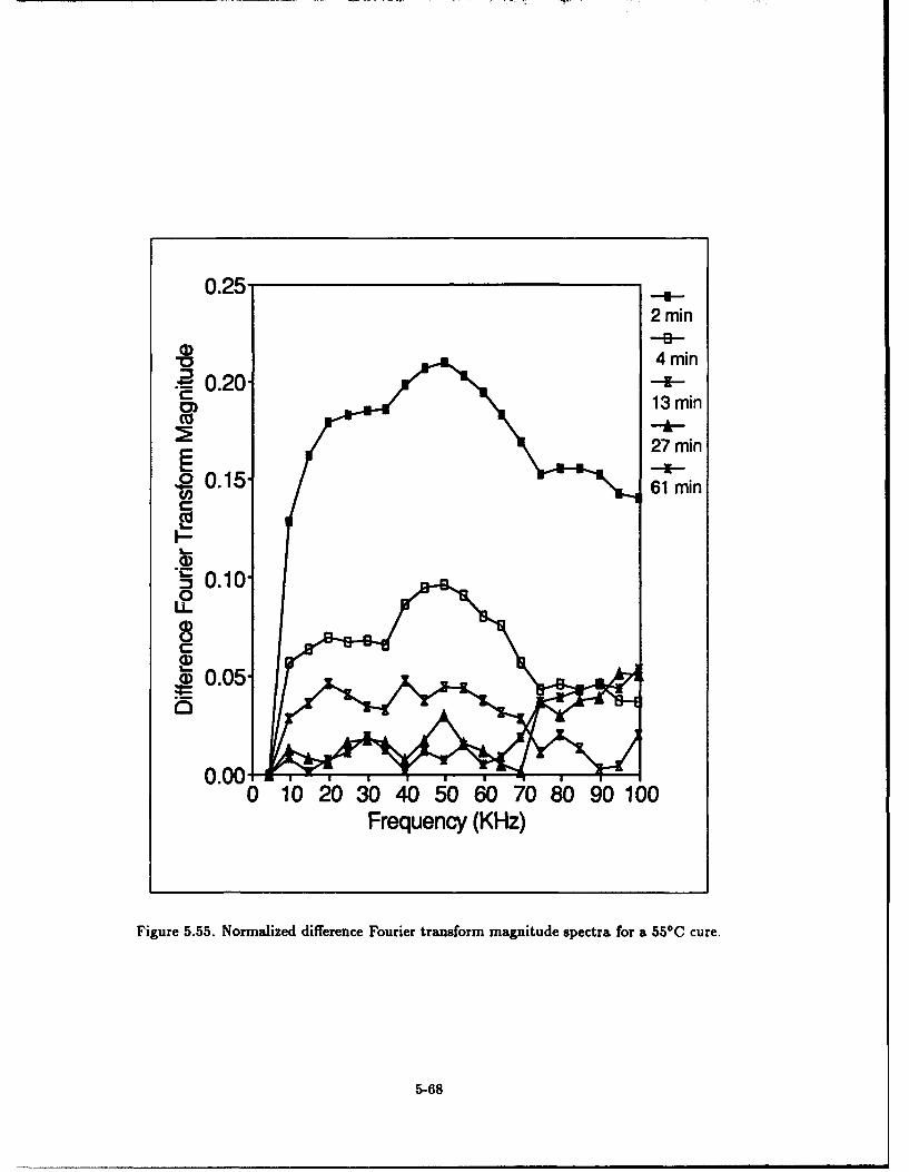
0.25-
0.20 -113min
E ~27min
'0 0.15 6 m
C
:3 0.10-02
S0.05-
0.00A0 1020 30 405060o7080 90100
Frequency (KHz)
Figure 5.55. Normalized difference Fourier transform magnitude spectra for a 55*C cure.
5-68
Summary
The IGEFET integrated circuits were received from MOSIS and electrically tested. Problems
were encountered with the multiplexer and demultiplexer circuits, and these circuits were
bypassed. The sensor elements were utilized in the IGEFET sensor experiments without further
amplification from the voltage follower or operational amplifier circuits.
Mechanical tests were conducted which indicated the range of temperatures for optimum
cure, and two of these were selected for this research (450C and 550C). Further mechanical tests
were performed to estimate the gelation times for these temperatures. Finally, torsional braid
analysis was conducted to determine the glass transition temperature for samples cured at 45 0 C
and 550C.
Electrical tests were conducted to evaluate the IGEFET as a resin cure sensor. Given the
results of the electrical tests, it was possible to estimate the gelation time of the resin. The
information that appeared to be most useful in the characterization of the material was the
impedance information. From a cure monitoring perspective, however, the gain-phase information
and the normalized difference Fourier transform spectra provided acceptable results. The data
associated with these measurements provided information regarding the gelation time of the resin,
and it was easily interpreted. In general, the gelation point was manifested by a decreased rate of
change in the measured electrical characteristic.
5-69
VI. Conclusions and Recommendations
Conclusions
An interdigitated gate electrode field-effect transistor (IGEFET) was designed, and its
elec*rical performance as a sensor for monitoring the cure cycle of an epoxy resin was evaluated.
The resin's molecular structure changed during its cure cycle. The physical change was indicated
by altered impedance characteristics, which the IGEFET detected. The research was conducted
in three phases. First, the IGEFET sensor was designed, and after it was fabricated, its oper-ting
characteristics were evaluated. Second mechanical characteristics of the resin were determined.
Finally, the sensor's performance as an in situ resin cure monitor was characterized.
The IGEFET sensor design consisted of a 3 x 3 array of sensor elements (SEs). Each sensor
element consisted of an interdigitated gate electrode (IGE) structure and an output amplifier. A
metallic ground plane was fabricated beneath the IGE structure to provide a degree of ambient
noise immunity, and also to facilitate characterizing the capacitance (to ground) of the IGE
structure. An input excitation signal was coupled to the driven-electrode of the IGE structure by
a demultiplexer, and the floating-electrode was connected to the input gate of the SE amplifier.
The SE amplifier was a 3-stage NMOS enhancement-mode device. The output of the SE amplifier
was coupled to the sensor's output buffers via a multiplexer. Two output buffers were included in
the design, a voltage follower, and an operational amplifier. In addition to these sub-circuits,
three capacitors were included in the design to facilitate characterizing the silicon dioxide layer
between the IGE structure and the ground plane. The reference element was identical to the SE,
except that the IGE structure was replaced by a solid metal plate to mimic the IGE structure's
impedance.
The multiplexer and demultiplexer did not operate correctly, and they could not be used.
Therefore, the only in situ signal amplification was provided by the sensor element amplifiers.
6-1
The mechanical characteristics of the resin were evaluated. The purpose of the evaluation
was to determine the range of optimum cure temperatures, to determine the gelation time for two
selected isothermal cure profiles, and to determine the glass transition temperature of the resin
cured at both selected temperatures. A dynamic spectrometer was utilized for all these
evaluations. The resin was cured with a ramped temperature profile to determine the optimum
range of cure temperatures. The resin's complex viscosity was measured using the parallel plate
mode of the dynamic spectrometer. The optimum cure temperature range corresponded to a
range of temperatures over which the resin exhibited a reduced viscosity. Two temperatures were
selected from this range (45*C and 55*C). Resin samples were then cured at each of these
temperatures (again in a parallel plate mode) to determine the resin's characteristic gelation time
for both isothermal cure profiles. Torsional bar analysis was performed using samples previously
cured at each of the selected temperatures, and the glass transition temperature was determined.
The glass transition temperature was 80C for the samples cured at 45*C, and was 70*C for the
samples cured at 55*C.
The IGEFET sensor was then evaluated as a resin cure monitor. This evaluation required
seven electrical performance measurements for each of the isothermal cure profiles. The direct
current resistance of the IGE structure was measured. The IGE structure's resistance was found
to increase rapidly during the cure, and it remained relatively constant after gelation. The
impedance of the IGE structure was measured, md it exhibited the same trend as the direct
current resistance. That is, a rapid change in the impedance characteristics, followed by relatively
little change after gelation, was observed. The electrical impedance measurements indicated that
loss mechanisms (due primarily to ionic conduction) dominate the cure initially, and later in the
cure, reactance dominates the impedance. The gain and phase delay of the IGE structure and the
IGEFET sensor's transfer functions were measured. The results of these measurements
corroborated the trends observed in other electric,*i measurements, specifically, the characteristic
decrease in the rate of change of the measured churacteristic after the gelation point was attained.
6-2
The gain and the phase delay changed dramatically during the initial stages of the cure cycle, but
they changed relatively little after the resin's gelation. The time- and frequency-domain response
of the IGEFET sensor were measured. They indicated a rapid decrease in energy transmitted
through the resin during the cure cycle, followed by little change after the gelation point was
attained. In general, the results of the IGEFET experiments corresponded well with the measured
mechanical and chemical characteristics of the resin, particularly the time-to-gelation.
The sensor was able to discern important differences between resins cured at different
temperatures. The low-temperature cure cycle (450C) and the high-temperature cure cycle
(550C) exhibited markedly different electrical characteristics. In general, resins cured at both
temperatures exhibited similar trends. However, the resin samples cured at 55*C were more lossy,
as indicated by the direct current resistance and the impedance measurements. The transfer
function of the resins cured at the higher temperature exhibited a much larger gain. These
characteristics are indicative of a softer material. The 55*C cure temperature was in the vicinity
of the resin's estimated glass transition temperature (70*C). The proximity of the glass transition
temperature to the cure temperature may have resulted in the marked differences between the
electrical characteristics of the two cure profiles.
In conclusion, the IGEFET sensor's utility as a resin cure monitor was demonstrated. It was
able to detect changes in the resin's impedance which were a direct consequence of the cure
process. It is clearly possible to estimate the resin's gelation time by analyzing the electrical data.
Additionally, the IGEFET sensor was able to discern differences in the electrical characteristics of
two resin samples cured at different temperatures.
Recommendations
The IGEFET sensor has clearly demonstrated utility as a resin cure sensor. Future research
should be directed toward further improvement of the IGEFET sensor design, and further
6-3
evaluation of the sensor with different resins. The specific recommendations for future research
include:
1. Eliminate glass cuts over signal lines from future designs. The glass cuts were intended to
facilitate the excision of malfunctioning sub-circuits. The original approach for the resin
cure evaluation was to coat the entire IGEFET sensor with resin. The glass cuts made this
impossible, however, since the resin effectively shorted the exposed signal lines.
2. Place fewer sensor elements on the integrated circuit die, and locate them closer to the
center of the integrated circuit. This would facilitate insulating the wire bonds, so that the
entire sensor could be coated with resin. The inclusion of nine sensor elements for the
IGEFET sensor applied to detect gaseous species is warranted, but it was of little utility for
the resin cure studies.
3. Provide separate voltage supply input lines for each subcircuit. Thus, if one voltage supply
line fails, only one sub- circuit is affected.
4. Use resins with lower viscosities. The resin used in this research was highly viscous in its
uncured state. This characteristic facilitated applying the resin to the IGE structure.
However, it precluded the possibility of performing tensile strength tests. The resin was too
viscous to permit removal of air bubbles from the material. This operation is typically
performed by exposing the resin to a vacuum. Providing the resin flows well, voids can be
removed from the resin in this manner. Tensile strength tests require materials without
discontinuities such as voids due to air bubbles. Since the material contained numerous
voids, it could not be tested for tensile strength.
5. Use resins with a higher relative permittivity. This would permit measurement of the resin's
low-frequency impedance after the gelation point, and it would facilisate a more complete
electrical characterization of the resin.
6-4
6. Develop an automated cure monitoring system. A simple program could be written to
measure the change in a particular electrical characteristic with time, and alert the
researcher when the gelation time has been attained.
7. Develop the capability to accomplish accurate ramped temperature profile cures cycles.
Ramped temperature profiles are more typical in practice than isothermal profiles.
6-5
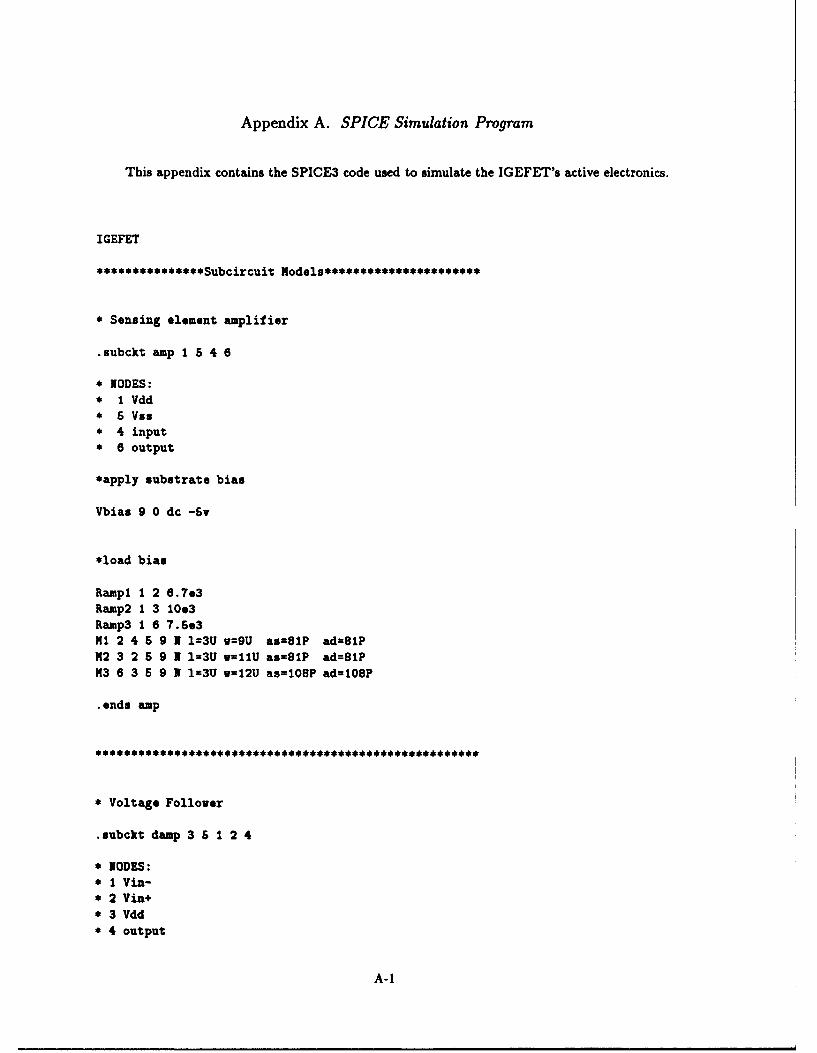
Appendix A. SPICE Simulation Program
This appendix contains the SPICE3 code used to simulate the IGEFET's active electronics.
IGEFET
***************Subcircujt Models**********************
* Sensing element amplifier
.subckt amp 1 5 4 6
* NODES:* 1 Vdd* 6 Vs.* 4 input* 6 output
*apply substrate bias
Vbias 9 0 dc -6v
*load bias
Rampl 1 2 6.7e3Ramp2 1 3 10e3Ramp3 1 6 7.5e3MI 2 4 5 9 1 1=3U v=9U as=8lP ad=81PM2 3 2 & 9 1 1=3U v=11U as=8lP ad=81PM13 6 3 5 9 N 1=:3U w-12U aslO08P ad=108P
.ends amp
*Voltage Follower
.subckt damp 3 5 1 2 4
* NODES:* 1 Yin-* 2 Via+* 3 Vdd* 4 output
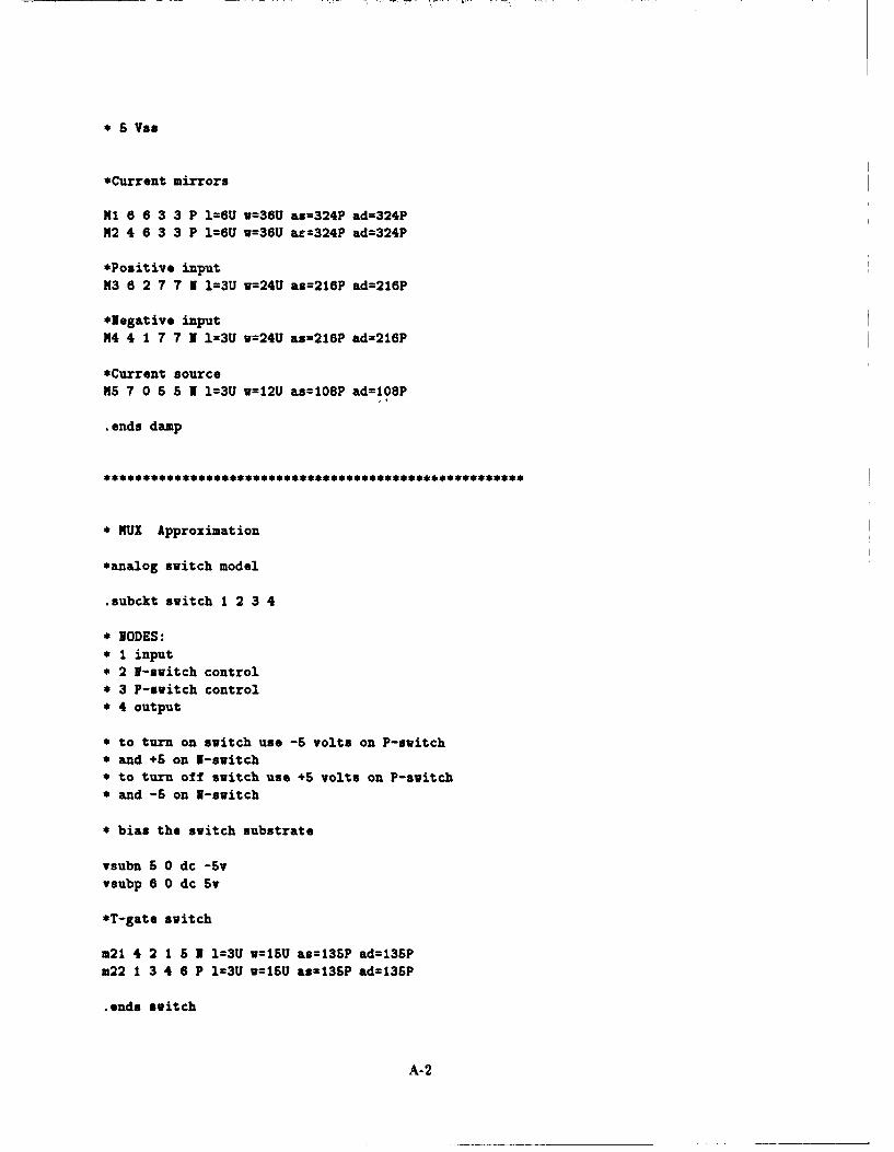
S Vs
*Current mirrors
MI 6 6 3 3 P 1=6U w=36U as=324P ad=324PM2 4 6 3 3 P 1=6U w=36U az=324P ad=324P
*Posit ive inputM13 6 2 7 7 N1l=3U w=24U as=216P ad=216P
*Negat ive inputM14 4 1 7 7 N1=3U w=24U as=216P ad=216P
*Current sourceMS5 7 0 5 5 1l=3U w=12U aslOS8P adlO08P
.ends damp
K UX Approximation
*analog switch model
.subckt switch 1 2 3 4
* NODES:* 1 input* 2 1-switch control* 3 P-switch control* 4 output
* to turn on switch use -5 volts on P-switch* and +6 on 1-switch* to turn off switch use +5 volts on P-switch* and -5 on 1-switch
* bias the switch substrate
vsubn S 0 dc -5vvsubp 6 0 dc 5v
*T-gate switch
m21 4 2 1 5 N 1=3U w15SU as=135P ad=135Pm22 1 3 4 6 P 1=3U w15SU as=136P ad=135P
.ends switch
A-2
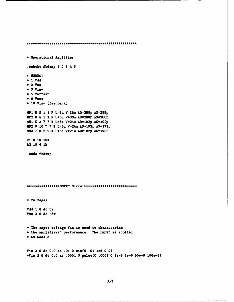
*Operational Amplifier
.subckt fbdamp 1 2 3 4 6
* NODES:* 1 Vdd* 2 Vas* 3 Vin+* 4 Voffset* 6 Vout* 10 Vin- (feedback)
MP1 6 5 1 1 P L=6u W=36u AD=288p AS=288pMP2 6 5 1 1 P L=6u W=36u AD=288p AS=288pNI 5 3 7 7 N L=6u W=24u AD=192p AS=192pMN2 6 10 7 7 1 L=6u W=24u AD=192p AS=192pM13 7 0 2 2 1 L=6u W=24u AD=192p AS=192P
RI 6 10 10kR2 10 4 1k
.ends fbdamp
*.***'**********IGEFET Circuit*************************
*Voltages
Vdd 1 0 dc SyVss 2 0 dc -5v
" The input voltage Vin is used to characterize" the amplifiers' performance. The input is applied" at node 3.
Yin 3 0 dc 0.0 ac .01 0 sinCO .01 1.6 0 0)'Yin 3 0 dc 0.0 ac .0001 0 pulse(0 .0001 0 le-6 le-6 60e-6 100e-6)
A-3
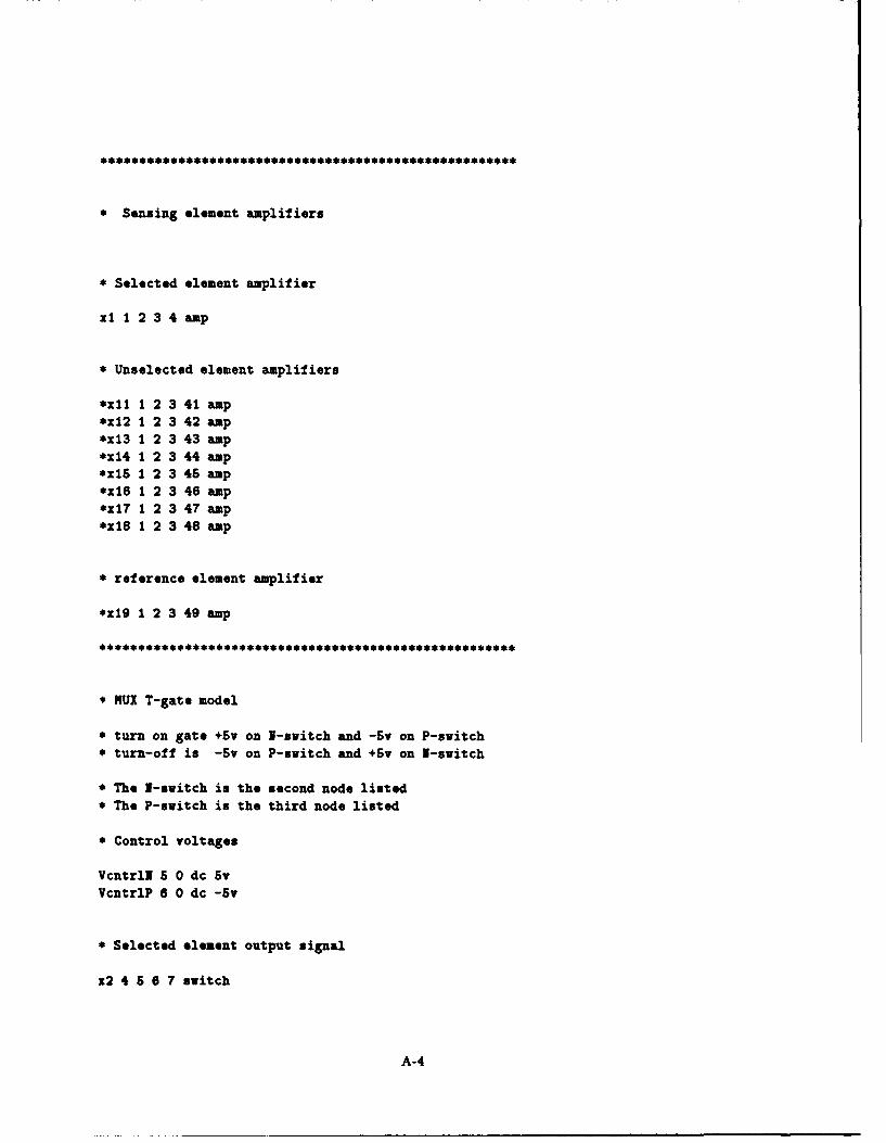
" Sensing element amplifiers
" Selected element amplifier
xl 1 2 3 4 amp
* Unselected element amplifiers
*x11 1 2 3 41 amp*x12 1 2 3 42 amp*x13 1 2 3 43 amp
*x14 1 2 3 44 amp
*x15 1 2 3 46 amp*x16 1 2 3 46 amp
*x17 1 2 3 47 amp
*x18 1 2 3 48 amp
* reference element amplifier
*x19 1 2 3 49 amp
* NUX T-gate model
" turn on gate +Sv on I-switch and -By on P-switch" turn-off is -Sv on P-switch and +Sv on I-switch
* The N-switch is the second node listed
" The P-switch is the third node listed
" Control voltages
Vcntrll 6 0 dc 5v
VcntrlP 6 0 dc -6v
* Selected element output signal
x2 4 6 6 7 switch
A-4
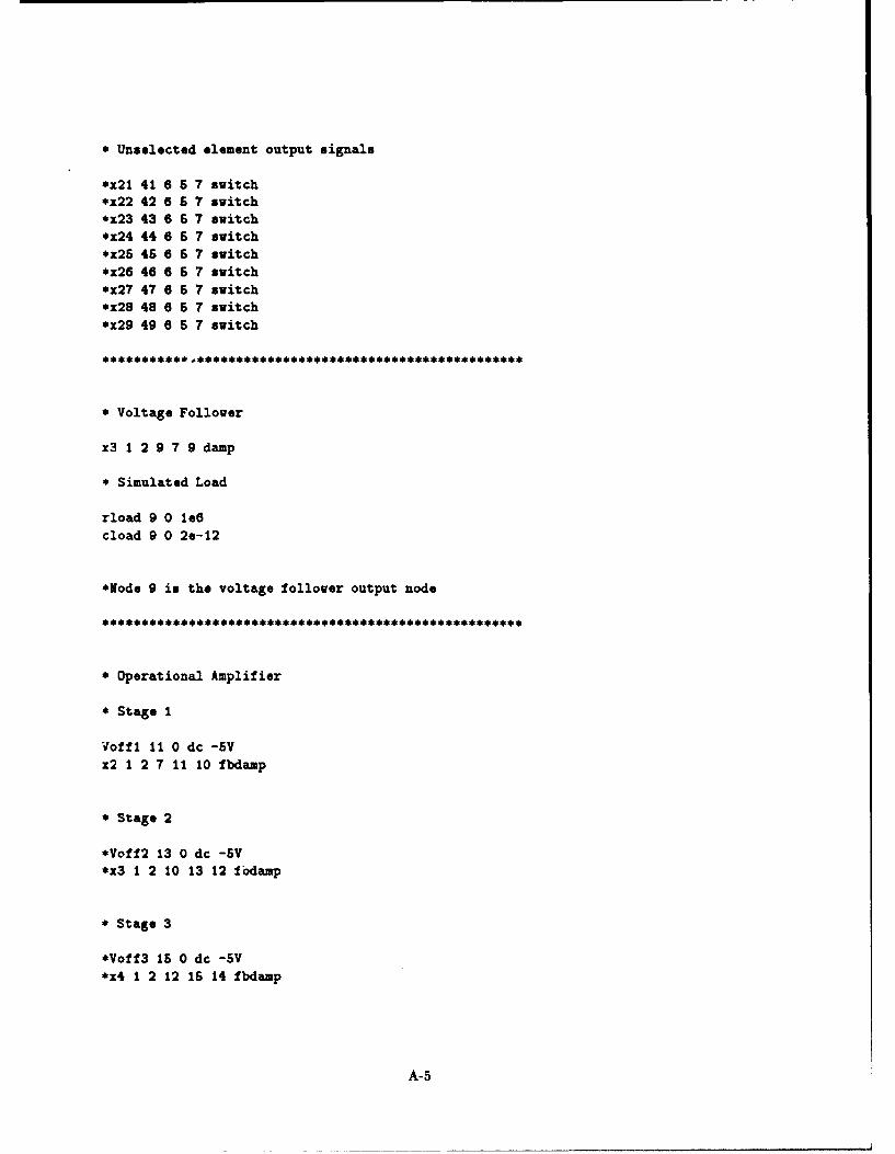
* Unselected element output signals
*x21 41 6 5 7 switch
*x22 42 6 5 7 switch*z23 43 6 6 7 switch
*x24 44 6 5 7 switch
*x25 45 6 5 7 switch
*x26 46 6 5 7 switch
*x27 47 6 5 7 switch
*x28 48 6 5 7 switch
*x29 49 6 5 7 switch
* Voltage Follower
x3 1 2 9 7 9 damp
* Simulated Load
rload 9 0 1e6
cload 9 0 2e-12
*Node 9 is the voltage follower output node
* Operational Amplifier
* Stage 1
Voffi 11 0 dc -SV
x2 1 2 7 11 10 fbdamp
* Stage 2
*Voff2 13 0 dc -SV
*x3 1 2 10 13 12 fodamp
* Stage 3
*Voff3 15 0 dc -SV
*x4 1 2 12 15 14 fbdamp
A-5
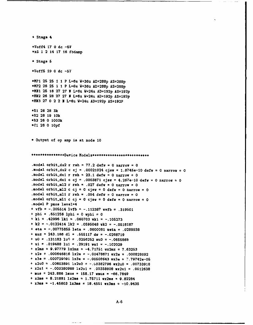
*Stage 4
*Voff4 17 0 dc -6V*xS 1 2 14 17 16 fbdamp
* Stage 6
*Voff5 19 0 dc -5V
*MP1 25 25 1 j P L=6u W=36u AD=288P AS=288p*MP2 26 25 1 1 P L=6u W=36u. AD=288p AS=288p*MN1 25 16 27 27 1 L=6u W=24u AD=192p AS=192p*MN2 26 28 27 27 N L=6u W=24u AD=192p AS=192P*MN3 27 0 2 2 N L=6u W=24u AD=192p AS=192P
*Rj 26 28 3k*R2 28 19 10k*R3 26 0 1000k*C1 28 0 l0pf
* Output of op amp is at node 10
***************Device Models**************************
.model orbit-.du2 r rsh =77.2 defy = 0 narrow = 0
.model orbit.du2 c cj = .00021024 cjnv = 1.8746.-10 defw 0 narrow =0
.model orbit.dul r rsh = 23.1 defw = 0 narrow = 0
.model orbit..duj c cj = .0003871 cjsw = 4.267.-10 defw 0 narrow 20
.model orbit.m12 r rsh =.027 deft = 0 narrow = 0
.model orbit.m12 c cj = 0 cjsw = 0 detv = 0 narrow = 0
.model orbit.mll r rsh =.064 defw = 0 narrow = 0
.model orbit.mll c ci = 0 cjsw = 0 defy = 0 narrow = 0
.model P pmos levei=4+ vfb = -. 205614 ivfb = -.112387 wvib = .319501+ phi = .651256 iphi = 0 iphi = 0+ kI = .42996 ikI = .060703 wkI = -.105273+ k2 =-.0122414 1k2 = .0595048 wk2 = -.0618187+ eta = -.00775855 iota = .0600061 veta = .0289938+ muz = 243.186 dl = .555117 dv = -.0268719+ uO = .131183 10O = .0256252 vu0 = -. 0655868+ iii = .019488 lul = .29191 viii = -.102029+ x2mz = 9.97779 ix2mz 2-4.71751 wx2mz = 7.63253+ x2. = .000646816 iz2e =-.00478671 wx2e = .000828692+ x30 = .000729091 1x3e =-.00508643 wx3e = 7.797429-O5+ x2uO =.00603891 1.x2uO =-.G0382796 vx2u0 .00733918+ x2ul =-.000380988 ix2ul = .00358808 wx2ul =.0012638
+ nun = 243.886 inns = 158.17 wmus = -66.7849+ x2ms =8.21881 ix2ma 1.75711 wx2ms 9.82284+ x3me -1.45603 1z3ms =18.4551 wx3us =-10.9435
A-6
+ x3ul = -.0168526 lx3ul = .00395624 wx3ul = .00243354+ tox = :0405 temp = 27 vdd = 5+ cgdo = 3.54981e-10 cgso = 3.54981e-10 cgbo = 6.52295e-10
+ xpart = 1+ nO = I inO = 0 wmO = 0+ nb = 0 lnb = 0 wmb = 0+ nd = 0 ind = 0 mud = 0+ rsh = 77.2 cj = .00021024 cjs = 1.8745e-10+ js = 0 pb = .7 pbsw = .7+ mj = .4434 mjs, = .2054 mdf = 0+ dell = 0.model I nmos level=4+ vfb = -.799628 lvfb = .0358389 mvfb = -.0770939+ phi = .760829 iphi = 0 wphi = 0+ ki = 1.09084 Ikl = .0195692 wkl = .503221
+ k2 = .00314699 ik2 = .0712321 wk2 = .0627686+ eta = -.00483964 leta = .0111977 weta = .0124884+ muz = 568.326 dl = .877101 dv = .124542+ uO = .0547895 luO = .0455111 muO = -.044398+ ul = .0202084 lul = .538695 mul = -.224314+ x2mz = 14.9246 ix2mz = -25.8935 wx2mz = 40.4786+ x2e = .000511543 ix2e = -.0078186 wx2e = -.00398345+ x3e = .000571135 ix3e = -.00175635 wx3e = -.00386746+ x2uO = .00269152 ix2uO = -.0119917 wx2uO = .0208939
+ x2ul = -.00220636 ix2ul = .0113252 mx2ul = .0138775+ mus = 572.011 inus = 339.156 wmus = -2.31256+ x2ms = 5.29578 lx2ms = -16.3472 wx2ms = 85.7263+ x3ms = -.60994 ix3ms = 64.5514 mx3ms = -32.2786+ x3ul = .00515024 lx3ul = .0574119 mx3ul = -.0347952+ tox = .0405 temp = 27 vdd = 5+ cgdo = S.60881e-10 cgso = 5.6088le-10 cgbo = 6.89101e-10
+ xpart = I+ nO = I inO = 0 wmO = 0+ nb = 0 nb = 0 wnb = 0+ nd = 0 lnd = 0 mud = 0+ rsh = 23.1 cj = .0003871 cjsw = 4.267e-10+ js = 0 pb = .8 pbsw = .8+ mj = .4626 mjsw = .348 wdf = 0+ dell = 0
.OPTIONS DEFL=3U DEFV=6U DEFAS=46P DEFAD=45P+ITLI=500 ITL4=30 ABSTOL=IOOP VNTOL=100U CHGTOL=E-14+NOPAGE RELTOL=.005 CPTIME=5000.WIDTH OUT=80
END
A-7
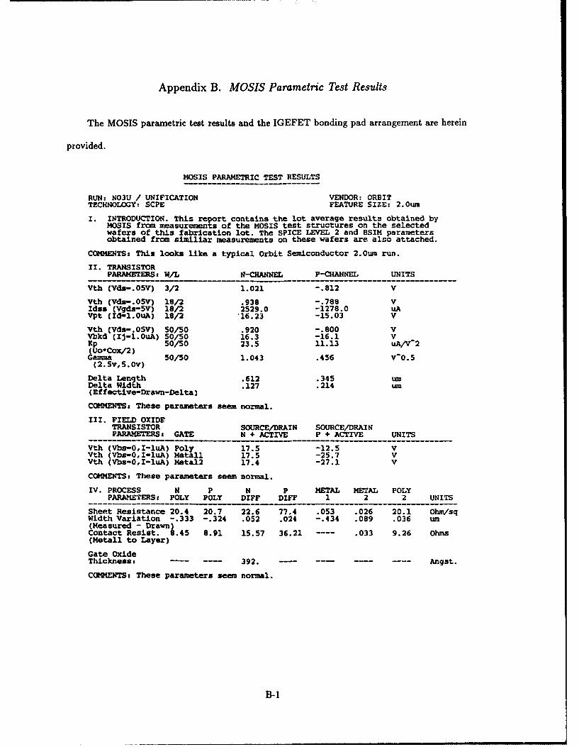
Appendix B. MOSIS Parametric Test Results
The MOSIS parametric test results and the IGEFET bonding pad arrangement are herein
provided.
MOSIS PARAMETRIC TEST RESULTS
RUN: N03U / UNIFICATION VENDOR: ORBITTECHNOLOGY: SCPE FEATURE SIZE: 2.Oum
I. INTRODUCTION. This report contains the lot average results obtained byMOSIS from measurements of the MOSIS test structures on the selectedwafers of this fabrication lot. The SPICE LEVEL 2 and BSIM parametersobtained from similiar measurements on these wafers are also attached.
COMMENTS: This looks like a typical Orbit Semiconductor 2.0uOn run.
I. TRANSISTORPARAMETES• W/L N-CHANNEL P-CHANNEL UNITS
Vth (Vds-. 05V) 3/2 1.021 -.812 V
Vth (Vds-.OSV) 18/2 .938 -.788 VIdss (Vgds-5V) 18/2 2529.0 -1278.0 uAVpt (Id-l.0uA) 18/2 '16.23 -15.03 V
Vth (Vds-.OSV) 50/50 .920 -.800 VVbkd (IJ-1.OuA) 50/50 16.3 -16.1 VKp 50/50 23.5 11.13 uA/V-2
(Uo*Cox/2)Gamma 50/50 1.043 .456 V-0.5(2.5v,5.Ov)
Delta Length .612 .345 umDelta Width .127 .214 um(Effective-Drawn-Delta)
COMMENTSZ These parameters seem normal.
III. FIELD OXIDETRANSISTOR SOURCE/DRAIN SOURCE/DRAINPARAMETERS: GATE N + ACTIVE P + ACTIVE UNITS
Vth (Vbs-0,I-luA) Poly 17.5 -12.5 VVth (Vbs-0,I-luA) Metall 17.5 -25.7 VVth (Vbs-0,I-luA) Meta12 17.4 -27.1 V
COMMENTS : These parameters seem normal.
IV. PROCESS N P N P METAL METAL POLYPARA'ETERSt POLY POLY DIFF DIFF 1 2 2 UNITS
Sheet Resistance 20.4 20.7 22.6 77.4 .053 .026 20.1 Ohm/sqWidth Variation -.333 -.324 .052 .024 -.434 .089 .036 um(Measured - Drawn)Contact Resist. 8.45 8.91 15.57 36.21 ---- .033 9.26 Ohms(Metall to Layer)
Gate OxideThickness- 392. -- ---- ---- Angst.
CCMMENTSt These parameters seem normal.
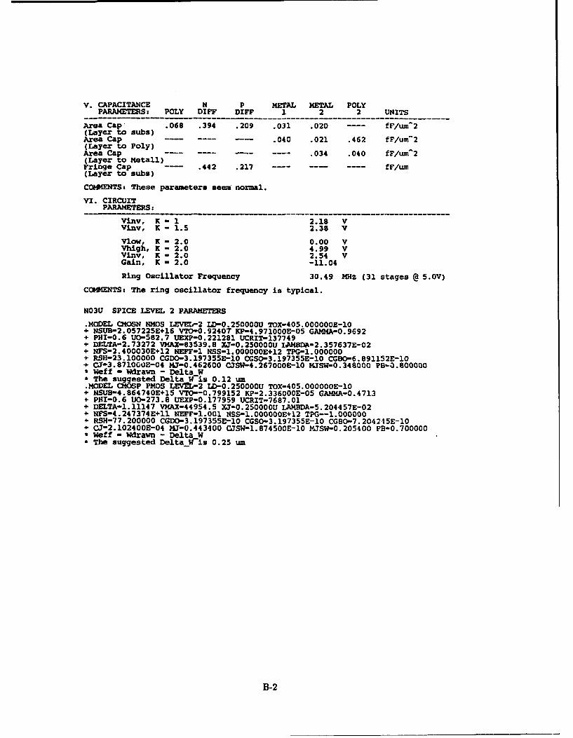
V. CAPACITAN4CE N P METAL METAL POLYPARAMETERS: POLY DIFF 01FF 1 2 2 UNITS
Area Cap .068 .394 .209 .031 .020 ---- fF/um-2(Layer tosubs)Area Cap - -- - - .040 .021 .462 fF/um-2(Layer to poly)Area Cap -- --- -- --- .034 .040 fF/um-2(Layer to Metall)Fringe Cap -- .442 .217 ----- fF/um(Layer to subs)
COHEXTSs These parameters seem normal.
VI. CIRCUITPARAMETERS.
Viy, K-i 2.1 V---Viny, K - 1. 2.38 V
Viow, K - 2.0 0.00 VThigh, K - 2.0 4.99 VViny, K - 2.0 2.54 VGain, K - 2.0 -11.04
Ring Oscillator Frequency 30.49 MHz (31 stages @5.OV)COMM3ENTS: The ring oscillator frequency is typical.
N03U SPICE LEVEL 2 PARAMETERS
.MODEL CMOSN NMOS LEVEL-2 LD-0.25000OU Tox-405.OOOOOOE-lO" NSU-2.057225E+16 VTO-0.92407 KP-4.971000E-05 GA1OMA-0.9692" P311-0.6 110-582.7 UEXP-0.221281 UCRIT-137749" DELTA-2.73272 VMAX-83539.8 XJ-0.250000U LAMBDA-2.357637E-02" NT5-2.400030E+12 NEFF-l NSS-l.000000E+12 TPG-1.000000" RSH-23.100000 CGDO-3.197355E-lO CGSO-3.197355E-10 CGBO-6.891152E-10" CJ-3.871000E-04 143-0.462600 CJSW-4.267000E-10 MJSW-0.348000 PB-3).800000" wet f - Wdrawn - Delta W" The suggested Delta W-7is 0.12 umn.MODEL CO0SP P1405 LEVEL-2 LD-0.250000U TOX-405.OOOOOOE-10" NSUE-4.864740E+15 VTO--0.799152 KP-2.336000E-05 GAMMA-0.4713" P311-0.6 110-273.8 UEXP-0.177959 UCRIT-7687.01" DELTA-1.11147 VMAX-44954.5 XJ-0.250000U LAMBDA-5.204457E-02" NFS-4.247374E+ll NEFF-1.001 NSS-l.000000E+12 TPG--l.000000" RSH-77.200000 CGDO-3.197355E-10 CGSO-3.197355E-10 CGBO-7.204215SE-l0" CJ-2.102400E-04 NJ-0.443400 CJSW-1.874500E-10 MJSW-0.205400 PB-0.700000" waff - Wdrawn - Delta W" The suggested DeltaW is 0.25 urn
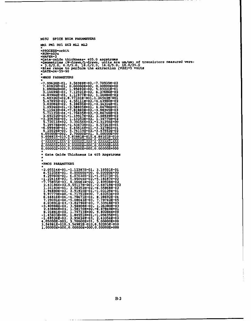
N403U SPICE BSIX PARAMETERS
NMI PHI DUI1 D(J2 Ma. )1.2
:PROCESS-orbit*RUNfl-n03u*WP.FER-2'Gate-oxide thickness- 405.0 angstroms*Geometries (W-drawn/L-drawn, units are urn/urn) of transistors measured were:* 3.0/2.0, 6.0/2.0, 18.0/2.0, 18.0/5.0, 18.0/25.0*Bias range to perform the extraction (Vdd)-5 volts*EDATE-04- 25-90
'NKOS PARAMETERS
-7. 99628E-01, 3. 58389E-02, -7. 70939E-027 .60829E-01, 0.0000E+00, 0. OOOOOE+001.09084E+00, I.592-2 5:03221E-013. 14699E-03, 7. 12321E-02, 6. 27686E-02-4 .83964E-03, 1.11977E-02, 1.24884E-025.68326E+02, 8.77101E-001,1.24542E-0015.47895E-02, 4 .55111E-02,-4.439S0E-022.02084E-02, 5.38695E-01,-2. 24314E-011.49246E+01,-2.58935E+01, 4 .04786E+015.11543E-04 ,-7.81860E-03,-3. 98345E-035.71135E-04 ,-1.75635E-03,-3 . 6746E-032.69152E-03,-1.19917E-02, 2. 08939E-02-2. 20636E-03, 1.13252E-02, 1. 38775E-025.72011E-02, 3. 39156E+02,-2.31256E+00S.29578E+00,-1. 53472E+Olo 8. 57263E+01
-6.09940E-01, 6.45514E+01,-3. 22786E+015.15024E-03, 5.74119E-02,-3.47952E-02
4 .05000E-002, 2.70000E+01, 5. 00000E+005.60881E-010, 5. 60881E-010,6.89101E-010l. 0000EOOO.. 0000E+000 ,0 .OOOOE40001. OOOOOE+00, 0. OOOOO+OOO, 0. 00000E40000.OOOOOE+000,0. 00000E4000,0.OOOQE+0000. 00000E+000,0. 00000E+000,.OOOOOE+000
*Gate Oxide Thickness is 405 Angstroms
'PHOS PARAMETERS
-2.05514E-01,-1.12387E-01, 3. 19501E-016. 51256E-01, 0. OOOOOE+00, 0. OOOOOE+004 .29960E-01, 6.07030E-02,-1. 05273E-01
-1.22414E-02, 5.95048E-02o-5.18187E-02-7.75855E-03, 6.00061E-02, 2.8993SE-022.43186E+02,5.55117E*-001..-2.68719E-0021. 31183E-01, 2. 56252E-02, -6. 55868E-021. 94880E-02, 2. 91910E-01,-1. 02129E-019.97779E*00,-4.71751E+00, 7.63253E+006.46816E-04 ,-4.78671E-03, 8.28692E-047.29091E-04 ,-5.08643E-03, 7.79742E-056.03891E-03,-3.82796E-03, 7.33918E-03-3. 80988E-04, 3. 5880SE-03, 1. 26380E-032.43886E+02, 1.58170E+02,-6. 67849E+016.21881E+00, 1.75711E+00, 9.892284E+00
-1.45603E+00, 1.84551E+01,-1.09435E+01-1.68526E-02, 3.95624E-03, 2.43354E-034. OSOOOE-002, 2. 70000E+01, 5. OOOOOE+003. 54981E-010, 3. 54981E-010, 6. 52295E-0101.0000 OE+-000, 0. OOOOOE+00, 0. OOOOOE+000
B-3
63-DRP-FRES/RFIT-ENG#Is 29753\GEFET
DIPB4P Ix PRRTS
B-4
Appendix C. Data Collection Software
This appendix contains a listing of the software used to collect the IGEFET performance
data.
Direct Current Data Collection Program
This program (dc.bas) was used to collect the direct current resistance data.
10 CLS20 PRINT "************************************************************"30 PRINT a**
35 PRINT "* DC RESISTANCE MEASUREMENT PROGRAM *"
40 PRINT "* *"
45 PRINT ************************************************************"50 PRINT ""
60 INPUT "PRESS RETURN WHEN READY TO CONDUCT MEASUREMENTS... ",NULL$
70 CLS100 '***************dc measurement program******************************110 1120 DEF SEG=AHC400130 INIT%=O140 TRANSMIT%=3150 RECIEVE%=6160 SEND%=9170 SPOLL%=12180 ENTERY,=21190 TARRAY%=200200 RARRY=203210 DMA2=206220 BUSADDRS%=21230 SYSCONT%=O240 1250 MY.ADDRY%=21260 SYS.CONTROL%=O270 CALL INIT%.(MY. ADDRY,SYS. CONTROL%)280 S$="UNL UNT"290 CALL TRANSMIT%(S$,STATUS%)300 K617%=27310 GOSUB 970 'GO TO TIMER ROUTINE320 OPEN "0",#1, "C:\EPOXY\DCBIAS.DAT"330 OPEN "0" .2, "C: \EPOXY\DCTIME.DAT"340 INPUT "MATERIAL: ",MATL$350 INPUT "TEMPERATURE: ".TEMPS
C-I
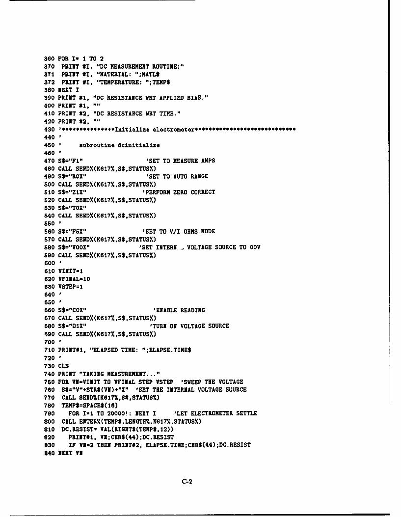
360 FOR In I TO 2370 PRINT #I, "DC MEASUREMENT ROUTINE:"371 PRINT #I. "MATERIAL: ";MATL$372 PRINT #I. "TEMPERATURE: ";TEMP$
380 NEXT I390 PRINT #1, "DC RESISTANCE WRT APPLIED BIAS."400 PRINT #1, ""
410 PRINT #2, "DC RESISTANCE WRT TIME."420 PRINT #2, ""430 '***************Initialize electrometer*****************************
440 1460 ' subroutine dcinitialize
460
470 S$="FI" 'SET TO MEASURE AMPS
480 CALL SEND%(K617%,S$,STATUS%)490 S$="ROX" 'SET TO AUTO RANGE500 CALL SEND%(K617%,S$,STATUS%)510 S$="Z1x" 'PERFORM ZERO CORRECT
520 CALL SEND%(K617%,S$.STATUS%)530 S$="TOX"540 CALL SEND%(K617%,S$,STATUS%)550 1560 S$="FSX" 'SET TO V/I OHMS MODE
570 CALL SEND%(K617%.,S$,STATUS%)580 S$="VOOX" 'SET INTERN.- VOLTAGE SOURCE TO OOV590 CALL SEND%(K617%.,S$,STATUS%)600 1610 VINIT=1620 VFINAL=1O630 VSTEP=I
640
650660 S$="COX" 'ENABLE READING670 CALL SEND.(K617%,S$,STATUS%)680 S$="01X" 'TURN ON VOLTAGE SOURCE690 CALL SEND%(K617..S$,SSTATUS%.)700 1710 PRINT#1, "ELAPSED TIME: ";ELAPSE.TIME$
720 1
730 CLS
740 PRINT "TAKING MEASUREMENT..."750 FOR V=VINIT TO VFINAL STEP VSTEP 'SWEEP THE VOLTAGE
760 S$="V"+STR$(VN)+"Z" 'SET THE INTERNAL VOLTAGE SUURCE770 CALL SEND%(K617%,S*,STATUS%)780 TEMP*=SPACES(16)790 FOR 1=1 TO 20000!: NEXT I 'LET ELECTROMETER SETTLE800 CALL ETER.(TEMP$,LENGTH%,K617SSTATUS%)810 DC.RESIST= VAL(RIGHT$(TEMPS, 12))820 PRINT#1, VN;CHR$(44);DC.RESIST
830 IF VI=2 THEN PRINT#2, ELAPSE.TIME;CHR$(44);DC.RESIST
840 NEXT VN
C-2
850860 S$2100111 'TURN OFF VOLTAGE SOURCE870 CALL SENDX617%.S$,STATUS%)880 S$="VOZ" 'SET VOLTAGE TO ZERO890 CALL SEND%(K6l7%.S$.STATUS%)900 S$="1C1X,, 'DISABLE READING910 CALL SEND%(KS17.S$,STATUSS)920'925 PRINT USING "###.##";ELAPSE.TIME926 PRINT ""
930 CLS :BEEP: INPUT "ANOTHER MEASUREMENT? EYJ * AN$940 IF AN*="N" OR AN$=n" THEN 950 ELSE 430950 CLOSE960 STOP970 #*************Timor initialization routine************************980990 ' subroutine timer initialization100010101020 ELAPSE. TIME$="00 :00:00.'1030 HOURS = 01040 MINUTES = 01050 SECONDS a 010601070 ' turn on elapse timer1080'10901100 BEGI1.TIME*=TIME$1110 DEGIN.HRS= VAL(LEFT$(BEGIN.TIME*,2))1120 BEGIN.MIN= VAL(MID$(BEGIN.TIME$.4,2))1130 BEGIN.SEC= VAL(RIGHT$(BEGIN.TIME$.2))1140 ON TIMER (1) GOSUB 1190 'gosub timer1150 TIMER ON116011170 RETURN1180
12001210 ' subroutine timer12201230 TIME. NOW$=TIME*1240 lOV. HRS= VAL(LEFTS (TIME. lOV$ *2))
1250 WOW.MIN= VAL(MID$(TIME.NOV$,4,2))1260 NOW.SEC= VAL(RIGHT* (TIME. IOW$,2))1270 SECONDS= NOW.SEC-BEGIN.SEC1280 IF SECONDS >= 0 THEE GOTO 1300 'gn two lines down1290 SECONDS=SECONDS+60: NOW. MINNIOW. MIN-11300 MINUTES=NOW . IN-BEGIE . IN1310 IF MINUTES >= 0 THEN GOTO 1330 'go two lines down1320 NINUTES=MINUTES+60: NOW. IRS=NOW. IRS-i1330 IF NOW.IRS<BEGIN.IRS THEN NOW.HRS=NOW.BRS+24
C-3
1340 HOURS=NOW.HRS-BEGIN. HRS1350 IF SECONDSC10 THEN SECONDS$=11O" + RIGHT$(STR$(SECOIDS) 1)1360 IF SECONDS >= 10 THEN SECONDS$=RIGHT$(STR$CSECOIDS),2)1370 IF NINUTESC10 TEEN MINUTESS="O" + RIGHT$(STR$(MINUTES),1)1380 IF MINUTES >= 10 THEN MINUTES$=RIGHTS(STR$(MINUTES) .2)1390 'EUAPSE.TIME$= STR$(HOURS) + :"+ MINUTES$ ': + SECONDS$14001410 'THE FOLLOWING ELAPSE.TIME IS IN MINUTES1420 ELAPSE.TIME=HOURS*60 + MINUTES + SECOIDS/60143014401450 RETURN
C-4
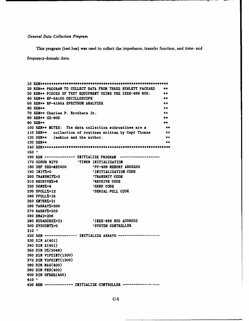
General Data Collection Program
This program (test.bas) was used to collect the impedance, transfer function, and time- and
frequency-domain data.
10 R *********************************************************20 REX** PROGRAM TO COLLECT DATA FROM THREE HEWLETT PACKARD **
30 REM** PIECES OF TEST EQUIPMENT USING THE IEEE-488 BUS. **
40 REM** HP-54100 OSCILLOSCOPE **
50 REM** HP-4195A SPECTRUM ANALYZER **
60 REM** **
70 REN** Charles P. Brothers Jr. **
80 REM** GE-90D **
90 REM** **
100 REM** NOTES: The data collection subroutines are a **
110 REM** collection of routines written by Capt Thomas **
120 REM** Jenkins and the author. **
130 REM** **
140 ******************************************************150160 REM -------------- INITIALIZE PROGRAM------------------170 GOSUB 8270 'TIMER INITIALIZATION180 DEF SEG=&HC400 'PC-488 MEMORY ADDRESS190 INIT%,=O 'INITIALIZATION CODE200 TRANSIT%=3 'TRANSMIT CODE210 RECEIVE%/=6 'RECEIVE CODE220 SEND%=9 'SEND CODE230 SPOLL%=12 'SERIAL POLL CODE240 PPOLL%=I5250 ENTERX=21260 TARRAY%=200270 RARRY%=203280 DMA2=206290 BUSADDRS%=21 'IEEE-488 BUS ADDRESS300 SYSCONT%=O 'SYSTEM CONTROLLER310 1320 REM --------------- INITIALIZE ARRAYS------------------330 DIM A(401)340 DIM X(401)350 DIM D%(2048)360 DIM V1POIIT(1300)370 DIM V2POINT(1300)380 DIM MAG(400)390 DIM PHS(400)400 DIM GFREQ(400)410 1420 RE ------------- INITIALIZE CONTROLLER----------------
C-5
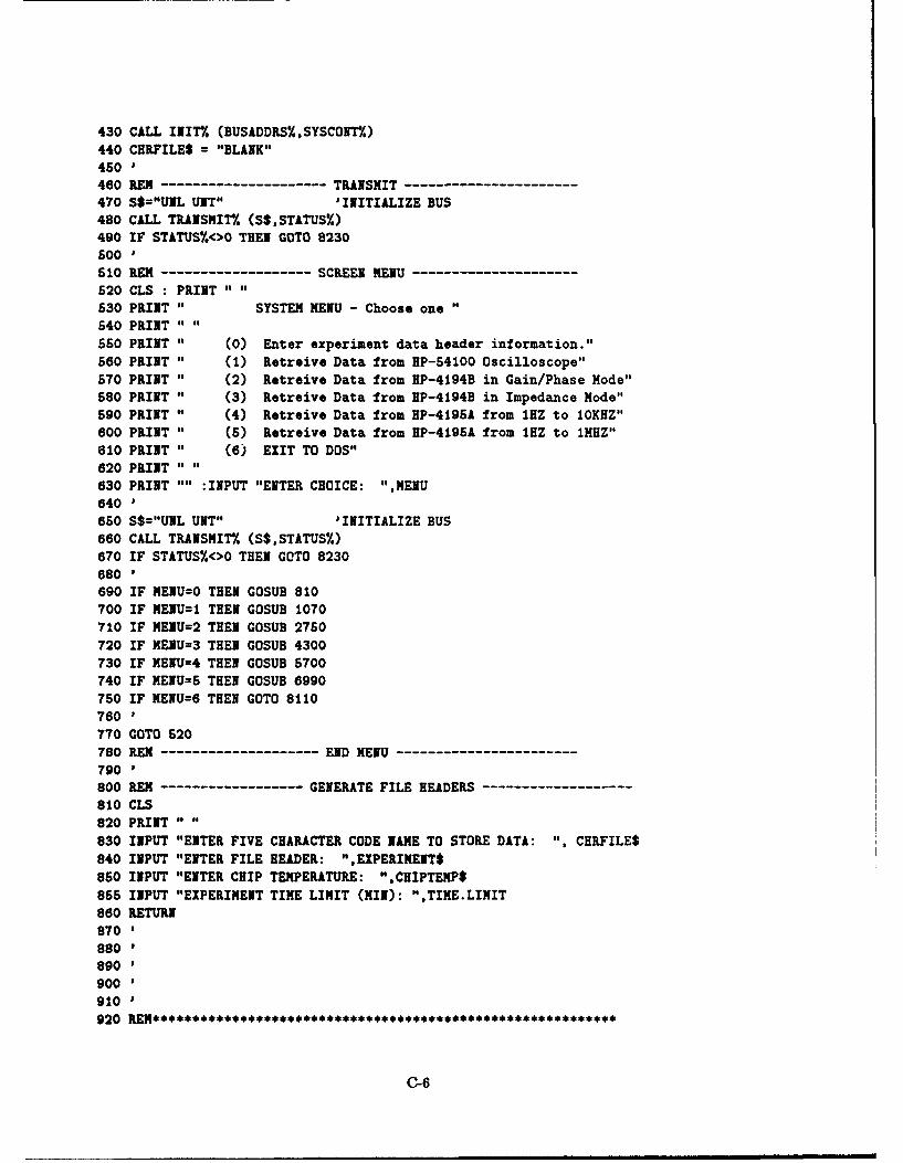
430 CALL INITY, (BUSADDRS%.SYSCONV/.)
440 CHRFILE$ = "BLANK"
450 '460 REM --------------------- TRANSMIT---------------------470 S$-"UNL UNT" 'INITIALIZE BUS480 CALL TRANSMIT/, (S$,STATUS%)
490 IF STATUS%,>0 THEN GOTO 8230500 *
510 REM ------------------- SCREEN MENU--------------------620 CLS : PRINT " "
530 PRINT " SYSTEM MENU - Choose one
540 PRINT "
50 PRINT " (0) Enter experiment data header information."
560 PRINT " (1) Retreive Data from HP-54100 Oscilloscope"
570 PRINT " (2) Retreive Data from HP-4194B in Gain/Phase Mode"
580 PRINT " (3) Retreive Data from EP-4194B in Impedance Mode"590 PRINT " (4) Retreive Data from HP-4195A from 1HZ to 10KHZ"
600 PRINT " (5) Retreive Data from HP-4195A from 1HZ to 1MHZ"
610 PRINT " (6) EXIT TO DOS"
620 PRINT " "
630 PRINT "" :INPUT "ENTER CHOICE: "MENU640 1
650 S$="UNL UNT" 'INITIALIZE BUS660 CALL TRANSMITX/ (S$,STATUS%)670 IF STATUS%<>O THEN GOTO 8230680 1690 IF MENU=O THEN GOSUB 810700 IF MENU=1 THEN GOSUB 1070
710 IF METU=2 THEN GOSUB 2750
720 IF MENU=3 THEN GOSUB 4300730 IF MENU=4 THEN GOSUB 6700
740 IF MENU=5 THEN GOSUB 6990
750 IF MENU=6 THEN GOTO 8110
760 1
770 GOTO 520780 RE -------------------- END MENU----------------------790800 REM ------------------ GENERATE FILE HEADERS------------------810 CLS
820 PRINT830 INPUT "ENTER FIVE CHARACTER CODE NAME TO STORE DATA: ", CHRFILE$
840 INPUT "ENTER FILE HEADER: ",EXPERIMENT$
850 INPUT "ENTER CHIP TEMPERATURE: ",CHIPTEMP$
856 INPUT "EXPERIMENT TIME LIMIT (MIN): ",TIME.LIMIT
860 RETURN
870880
890
900
910
920 R ***********************************************************
0-8
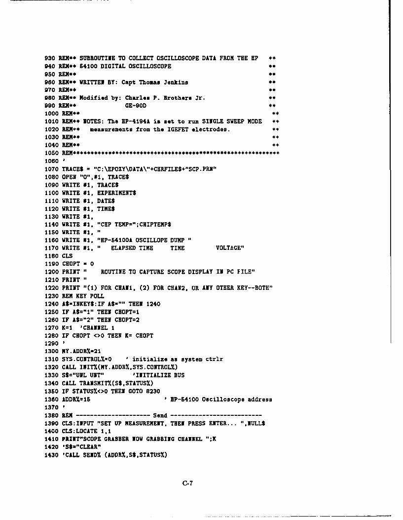
930 REX** SUBROUTINE TO COLLECT OSCILLOSCOPE DATA FROM THE HP *
940 REK** 54100 DIGITAL OSCILLOSCOPE *
950 REM** *
960 REX** WRITTEN BY: Capt Thomas Jenkins *
970 REX** *
980 REX** Modified by: Charles P. Brothers Jr. *
990 REX** GE-9OD c1000 REX** *
1010 RENCC NOTES: The HP-4194A is set to run SINGLE SWEEP MODE *
1020 REM** measurements from the IGEFET electrodes. *
1030 REM** c1040 REM** *
1050 R~ccececceeccccececccc*ccccccc~10601070 TRACE$ = "IC: \EPOXY\DATA\"'+CHRFILE$+"SCP.PU"I1080 OPEN "0'-,#1, TRACE$1090 WRITE #1, TRACES1100 WRITE #1, EXPERIMENTS1110 WRITE #1, DATES1120 WRITE #1, TIMES1130 WRITE #1,1140 WRITE #1, --CIP TEMP=";CHIPTEMPS1150 WRITE #1, --1160 WRITE #I, --HP-64100A OSCILLOPE DUMP"1170 WRITE #1, " ELAPSED TIME TIME VOLTAGE"1180 CLS1190 CHOPT =01200 PRINT " ROUTINE TO CAPTURE SCOPE DISPLAY IN PC FILE"1210 PRINT"1220 PRINT "(1) FOR CHANI, (2) FOR CHAN2, OR ANY OTHER KEY--BOTH"-1230 RUM KEY POLL1240 AS=INKEYS:IF A5"" THEN 12401250 IF AS="11 THEN CHOPT=11260 IF A$="2" THEN CHOPT=21270 K=1 'CHANNEL 11280 IF CHOPT <>0 THEN K= CHOPT12901300 MY.ADDR%.=211310 SYS.CONTROL%0 ' initialize as system ctrlr1320 CALL IIIT%,(MY.ADDR%.,sYs.COITROLY.)1330 S$5"UNL UNT"1 'INITIALIZE BUS1340 CALL TRANSMIT%.(S$,STATUS%)1350 IF STATUS%<O THEN GOTO 82301360 ADDRYz15 ' P-64100 Oscilloscope address13701380 RUX--------------------- Send --------------------------1390 CLS:INPUT "SET UP MEASUREMENT, THEN PRESS ENTER ... ",NULL$1400 CLS:LOCATE 1,11410 PIT11SCOPE GRABBER NOW GRABBING CHANNEL ";K1420 'SS="CLEAR041430 'CALL SEND% (ADDR%,SS,STATUS,)
C- 7
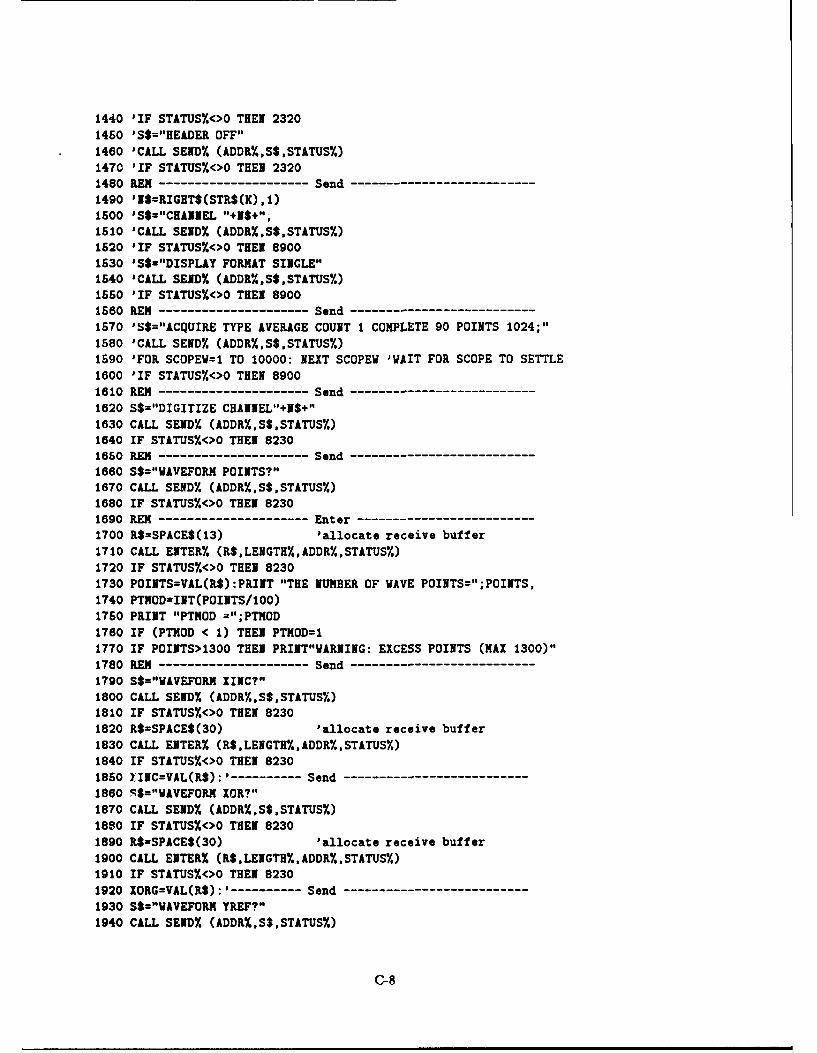
1440 'IF STATUS%<>O THEN 2320
1450 'S$="HEADER OFF"
1460 'CALL SEND% (ADDR/.,S$,STATUS.)1470 'IF STATUS%<>O THEN 23201480 REM --------------------- Send--------------------------1490 'I$=RIGHT$(STR$(K),4)1500 'SSWCHANNEL "+N$+",1510 'CALL SEND (ADDR%.S$.STATUS%)1520 'IF STATUS%<>O THEN 8900
1530 'S$="DISPLAY FORMAT SINGLE"1540 'CALL SENDD% (ADDR%,S$,STATUS%)
1550 'IF STATUS%<>O THEN 89001660 REM --------------------- Send-------------------------
1570 'S$="ACQUIRE TYPE AVERAGE COUNT 1 COMPLETE 90 POINTS 1024;"1580 'CALL SEND% (ADDRY,S$,STATUS%)1590 'FOR SCOPEW=1 TO 10000: NEXT SCOPEW 'WAIT FOR SCOPE TO SETTLE1600 'IF STATUS%<>O THEN 89001610 REM --------------------- Send-------------------------1620 S$="DIGITIZE CHANNEL"+N$+"1630 CALL SEND% (ADDR%,S$.STATUS%)1640 IF STATUS<>O THEN 8230160 REM --------------------- Send-------------------------1660 S$="WAVEFORM POINTS?"
1670 CALL SEND. (ADDR.S$,STATUS%)1680 IF STATUS%<>O THEN 82301690 REM --------------------- Enter-------------------------1700 R$=SPACE$(13) 'allocate receive buffer1710 CALL ENTER% (R$,LENGTH%,ADDR%,STATUS%)1720 IF STATUS%<>O THEN 82301730 POINTS=VAL(R$):PRINT "THE NUMBER OF WAVE POINTS=";POINTS,1740 PTMOD=INT(POINTS/100)1750 PRINT "PTMOD =";PTMOD1760 IF (PTMOD < 1) THEN PTMOD=11770 IF POINTS>1300 THEN PRINT"WARNING: EXCESS POINTS (MAX 1300)"1780 REM --------------------- Send-------------------------1790 S$="WAVEFORM IINC?"1800 CALL SEND (ADDR.,S$,STATUS%)1810 IF STATUS%<>O THEN 82301820 R$=SPACE$(30) 'allocate receive buffer
1830 CALL ENTER (R$.LENGTH%,ADDRY.,STATUS%)1840 IF STATUS%<>O THEN 82301850 YIIC=VAL(R$):' ---------- Send-------------------------1860 S$="WAVEFORM XOR?"
1870 CALL SEND% (ADDR%,S$,STATUS%)1880 IF STATUS%<>O THEY 82301890 R$=SPACE$(30) 'allocate receive buffer1900 CALL ENTER (R$,LENGTH,ADDR.STATUS%)1910 IF STATUS%<>O THEN 82301920 ZORG=VAL(R$):' ---------- Send-------------------------1930 S$="WAVEFORM YREF?"1940 CALL SEND (ADDR%,S$,STATUSY,)
C-8
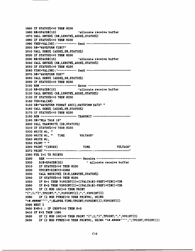
1950 IF STATUS%<>O THEN 82301960 R$=SPACE$(13) 'allocate receive buffer1970 CALL ENTER% (R$,LENGTH%,ADDR%,STATUS%)1980 IF STATUS<>O THEN 82301990 YREF=VAL(R$):'----------- Send-------------------------2000 S$="WAVEFORM YINC?"2010 CALL SEND. (ADDRY.,S$,STATUS%)2020 IF STATUS%<>O THEN 82302030 R$=SPACE$(13) 'allocate receive buffer2040 CALL ENTERY. (R$,LENGTH%,ADDR%,STATUS%)2050 IF STATUS%<>O THEN 82302060 YINC=VAL(R$):' ----------- Send-------------------------2070 S$="WAVEFORM YOR?"2080 CALL SEND% (ADDR,S$,STATUS%)2090 IF STATUS%<>O THEN 82302100 REM --------------------- Enter------------------------2110 R$=SPACE$(13) 'allocate receive buffer2120 CALL ENTER. (R$,LENGTH.,ADDR. ,STATUS.)2130 IF STATUS%<>O THEN 82302140 YOR=VAL(R$)2150 S$="WAVEFORM FORMAT ASCII;WAVEFORM DATA? "
2160 CALL SEED (ADDRY.,S$,STATUS%)2170 IF STATUS%<>O THEN 82302180 REM --------------------- TRANSMIT---------------------2190 S$="MLA TALK 15"
2200 CALL TRANSMITIZ (S$,STATUS%)2210 IF STATUS%<>O THEE 82302220 WRITE #1, "2230 WRITE #1. " TIME VOLTAGE"2240 WRITE #1,2250 PRINT " "
2260 PRINT "(INDEX) TIME VOLTAGE"2270 PRINT " -----------------------
2280 FOR I=1 TO POINTS2290 REM --------------------- Receive-----------------------2300 RI$=SPACE$(32) ' allocate receive buffer2310 IF STATUS%<>O THEN 82302320 TPOINT=XINC*I+XORG2330 CALL RECEIVEh (RI$,LENGTHY.,STATUS.)2340 IF STATUS%<>O THEN 82302350 IF K=1 THEN VlPOINT(I)=((VAL(Rl$)-YREF)*YINC)+YOR2360 IF K=2 THEN V2POINT(I)=((VAL(R1$)-YREF)*YINC)+YOR2370 IF (I MOD 100)=0 THEN PRINT"("; I;")" ,TPOINT; ",",VIPOINT(I) ;"," ,V2POINT(I)
2380 IF (I MOD PTMOD)=0 THEN PRINT#1, USING"+#.##### ... ,";ELAPSE.TIME;TPOIT;VIPOINT(I);V2POINT(I)
2390 NEXT I2400 K=K+1 : IF CHOPT<>O THEN K=32410 IF K<3 THEN 13802420 IF (I MOD 100)=0 THEN PRINT "(";I;")",TPOINT;",",VPOINT(I)2430 IF (I MOD PTMOD)=O THEN PRINT#1, USING "+#.#####...,";TPOINT;VPOINT(I)
C-9
2440 "2450 INPUT "DO YOU VANT TO TAKE ANOTHER MEASUREMENT? EY] ",AI$2460 IF AN$="N" OR AN$z"n" TEEN 2470 ELSE 12702470 S$="LOCAL"2480 CALL SEND% (ADDR%,S$,STATUS%)2490 S$="UNL UNT"2500 CALL TRANSMIT. (S$.STATUS%)
2510 IF STATUS%<>O THEN 8230
2520 CLOSE
2530 PRINT"FINISHED"2540 RETURN25502560257025802590
2600 REM*****************************************************
2610 REM** ROUTINE TO COLLECT GAIN PHASE DATA FROM THE HP-4194B **
2620 REM** GAIN PHASE ANALYZER. **
2630 REM** **2640 REMe* WRITTEN BY: Capt Thomas Jenkins **
2650 lR.3e **
2660 REM** Modified by: Charles P. Brothers Jr. **
2670 REM** GE-90D **
2680 REM** **
2690 REM** NOTES: The HP-4194A is set to run GAIN PHASE **2700 REN* measurements from the IGEFET electrodes. *
2710 REM**2720 *e **
2730 REC, e**e** ***ee**e****C********
2740
2750 CLS2760 PRINT," EP4194A GAIN PHASE DATA TRANSFER
2770 OPEN "0"*, #1, "C: \EPOIY\DATA\"+CHRFILE$+"GP"+STR$ (0)+". PRN"2780 OPEN "0", #2, "C: \EPOXY\DATA\"+CERFILE$+"GP"+STR$(1)+". PRN"2790 -
2800 ' --------- GP-IB ADDRESSES OF INSTRUMENTS------------------2810 HP4194%=17: HP4192%=9: PRINTERY.=I: MY.ADDR.=21: K617%.=27
2820 SWITCH%=28
2830 1
2840 SYSCON%=0 'PC488 ACTS AS CONTROLLER2850 CALL INIT%(MY.ADDR%,,SYSCON%)
2860 '
2870 PRINT " "
2880 PRINT "SETTING-UP 4194 FOR GAIN PHASE MEASUREMENTS -- WAIT..."
2890 1
2900 SS="RS2" 'UNMASK AND ENABLE BITI FOR SRQ2910 CALL SJD %(P4194%,S$,STATUS%)2920 S$="FNC2" 'SET 4194 TO GAIN PHASE MODE
2930 CALL SEND%(HP4194%.S$,STATUS%)2940 S$="P1S2" 'SET PHASE SCALE TO EXPANSION MODE
C-10
2950 CALL SEND%(HP4194%,S$STATUS%)
2960 SS="SWM2" 'SET SWEEP MODE TO SINGLE
297O CALL SEND%(HP4194%,SS,STATUS%)2980 SS="SWT2" 'SET TO LOG SWEEP2990 CALL SENDY,(HP4194%,SS,STATUS%)
3000 S$="MCFI" 'TURN MARKERS ON3010 CALL SENDY%(HP4194%,SS,STATUS%)
3020 SS="ZIT1" 'TEST CHANNEL TO 1 MOHMS
3030 CALL SEND%(HP4194%,SS,STATUS%)
3040 S='°ZIR1" 'TEST CHANNEL TO I MOHMS
3050 CALL SEND%(HP4194%,S$,STATUS%)3060 SS="ATT2" 'REFERENCE CHANNEL 20DB
3070 CALL SEND%(HP4194%,S$,STATUS%)
3080 S$="ATR2" 'REFERENCE CHANNEL 20DB3090 CALL SEND.(HP4194%,SS,STATUS%)3100 S$="START=IOHZ" 'STRT SWEEP AT IOHZ3110 CALL SEND%(HP4194%,S$,STATUS%)3120 S$="STOP=1OOOHZ" 'SWEEP TO 1KHz3130 CALL SEND%.(HP4194%.SS.STATUS%)3140 S$="NOA=4" 'SET AVERAGES TO 43150 CALL SEND%.(HP4194%,S$,STATUS%)3160 '3170 CLS3180 INPUT "PERFORM THE OFFSET REF STORE, THEN RETURN", NULLS
3190 '
3200 CALL INIT*/%(MY.ADDR*,,SYSCON ,)3210 CALL SPOLL.(HP4194%,POLL.,STATUS%) 'MAKE SURE SRQ NOT SET3220 SS="ITM2" 'SET INTEGRATION TIME TO 10 mSEC3230 CALL SEND%(HP4194%,S$,STATUS%)3240 SS="X?'" 'READ IN FREQUENCY POINTS3250 CALL SEND%(HP4194%.,SSSTATUS%)3260 IF STATUS%<>O THEN 82303270 SS="MLA TALK 17" '4194 TO OUTPUT3280 CALL TRANSMIT%(SS,STATUS%)3290 TEMPS=SPACES(15)3300 FOR 1=0 TO 400
3310 CALL RECEIVE.(TEMPSLENGTH.,STATUS%)3320 GFREQ(I)=VAL(LEFTS(TEMPS, 12))3330 NEXT I3340 '3350 CLS3360 INPUT "NUMBER OF ELECTRODES TO BE SAMPLED: ",NELECT3370 FOR NIz TO NELECT3380 GAINPHS = +CHRFILES+"GP"+STRS(NELECT)+".PRN"3390 WRITE N. GAINPHS3400 WRITE #1, EXPERIMENTS3410 WRITE #N. DATES3420 WRITE #N, TIMES3430 WRITE #N,3440 WRITE #N. "CHP TEMP=";CHIPTEMPS
3450 WRITE #N,
C-1l
3460 WRITE #N, "HP-4194A GAIN PHASE DUMP3470 WRITE #N, "3480 WRITE #N, "ELAPSED TIME, ELECTRODE, FREQUENCY, Z-MAG, PHASE"3490 WRITE #N, "3500 NEXT N3610 CLS3620 FOR N=O TO (NELECT-1) 'LOOP THROUGH THE NUMBER OF ELECTRODES3530 PRINT "CONNECT ELECTRODE ";N,3540 PRINT "SET OSC LEVEL, ENSURE OFFSETS ARE TURNED ON, MAKE OTHER"3550 INPUT at NECESSARY CHANGES, THEN HIT RETURN.",NULL$3560 GOSUB 3780 ' GO GET DATA3670 F=N+I3580 INPUT "YOU LIKE? EY] ",ANS3590 IF AN$="N" OR ANI"n" THEN 353036003610 F=N+13620 PRINT#F, "ELAPSED TIME : ";ELAPSE.TIME3630 FOR I= 0 TO 4003640 IF (I MOD 4)=0 THEN PRINT#F, USING"+#.####-....";ELAPSE.TIXE;N;GFREQ(I) ;AG(I);PHS(I)3650 IF (I MOD 100) = 0 THEN PRINT N,GFREQ(I),MAG(I),PHS(I)3660 NEXT I3670 NEXT N ' LOOP THROUGH THE ELECTRODE3680 INPUT "TAKE ANOTHER MEASUREMENT? EY] ",ANSWER$3690 IF ANSWER$"N" OR ANSWER$="n" THEN 3700 ELSE 33503700 CLOSE3710 S$="UNL UNT" 'INITIALIZE BUS3720 CALL TRANSMIT*/ (S$,STTUS%)3730 IF STATUS%.<>O THEN GOTO 82303740 RETURN3750 13760 '------------ HP4194 DATA INPUT ROUTINE----------------37703780 CALL SPOLL.(HP4194%,POLL%,STATUS%) 'MAKE SURE SRQ IS NOT SET3790 S$="SWTRG" 'PERFORM SINGLE SWEEP3800 CALL SEND%(BP4194,S$,STTUS.)3810 CALL SPOLL%(HP4194%,POLL7,,STATUS%) 'IS SWEEP COMPLETE?3820 IF ((POLL% AID 64) <> 64) THEN 3810 'IF NOT CONTINUE POLL3830 P3840 S$="AUTOA" 'AUTOSCALE DISPLAY A3850 CALL SEND%(HP4194%,S$,STATUS%)3860 S$="AUTOB" 'AUTOSCALE DISPLAY B3870 CALL SEND%(HP4194%,S$,STATUS%)3880 S$="A?" 'READ IN MAG VALUE3890 CALL SEND%(HP4194%,S$,STATUS%) 'FROM THE ARRAY REG A3900 '3910 S$= "MLA TALK 17"
3920 CALL TRANSMIT%,(S$,STATUS%)3930 TEMP$= SPACES(13)3940 FOR I = 0 TO 4003960 CALL RECEIVE%(TEMP$,LENGTH%, STATUS%)
C-12
3960 lAG(I)=VAL(LEFT$(TEMP$,12)) 'EXTRACT MAG VALUE
3970 NEXT I
3980 1
3990 S$="B?" 'READ IN PHASE FROM ARRAY REGISTER B4000 CALL SEND%(HP4194%,S$,STATUS%)4010 S$= "lILA TALK 17"4020 CALL TRANSMIT'(S$,STATUSY.)
4030 FOR I= 0 TO 400
4040 CALL RECEIVE. (TEMP$, LENGTH., STATUS.)
4050 PHS(I)= VAL(LEFT$(TEMP$,12)) 'EXTRACT PHASE VALUE4060 NEXT I
4070 14080 CALL SPOLLY,(HP4194%,POLL%,,STATUS%) 'MAKE SURE SRQ NOT SET
4090 RETURN4100
4110
4120
4130
4140
4150 R***********************************************************4160 REM** ROUTINE TO COLLECT IMPEDANCE DATA FROM THE HP-4194B **4170 REM** IMPEDANCE / GAIN PHASE ANALYZER. **
4180 REM** **
4190 REM* WRITTEN BY: Capt Thomas Jenkins **4200 REM** **
4210 REM** Modified by: Charles P. Brothers 3r. **
4220 REX** GE-90D **
4230 REM** **
4240 REM* NOTES: The HP-4194A is set to run IMPEDANCE **
4250 REM** measurements from the IGEFET electrodes. **
4260 REM** **
4270 REM** **
4280 REM***,********,*****,**.*,, ***************************** *4290
4300 CLS
4310 PRINT," HP4194A IMPEDANCE DATA TRANSFER "
4320 14330 '------ GP-IB ADDRESSES OF INSTRUMENTS------------------4340 HP4194%=17
4350 HP4192%=9
4360 PRINTER%14370 K617%=27
4380 SWITCH%=28
43q0 1
4400 PRINT "
4410 PRINT "SETTING-UP 4194 FOR IMPEDANCE MEASUREMENTS -- WAIT..."
4420 14430 S$="RQS2" 'UNMASK AND ENABLE BITI FOR SRQ4440 CALL SEND%(NP4194X,S$,STATUS.)4450 S$="FNCI" 'SET 4194 TO IMPEDANCE MODE
4460 CALL SEND%(HP4194%.SS,STATUS%)
C-13
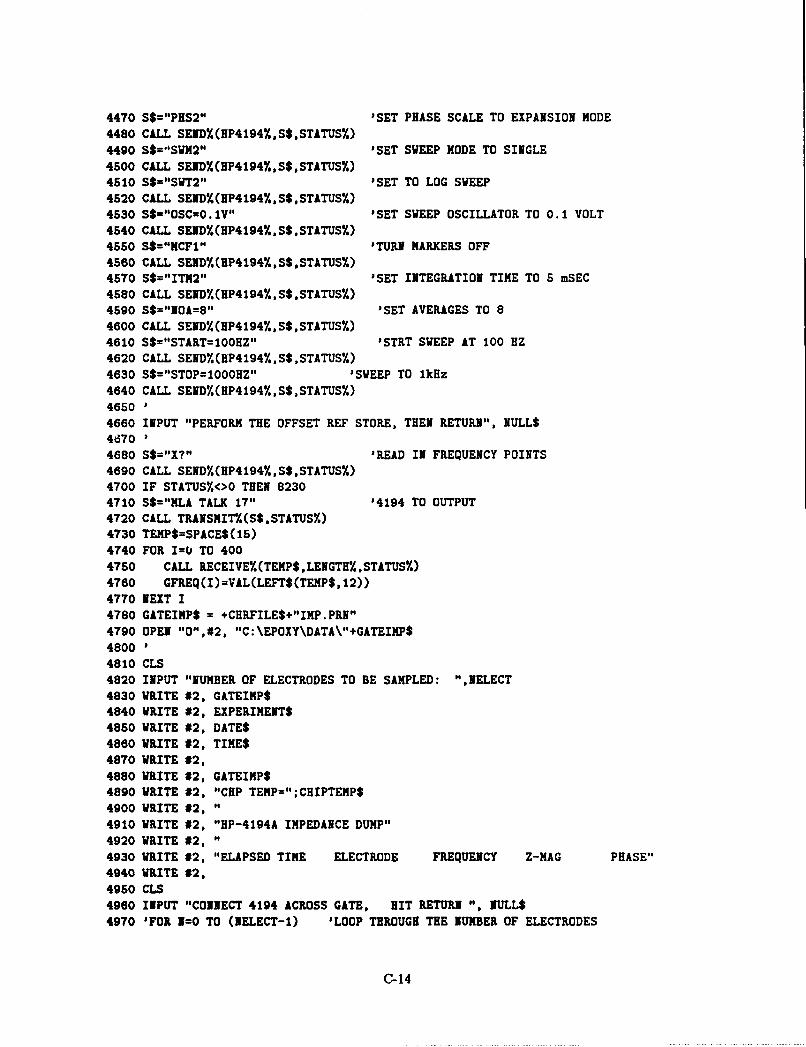
4470 S$="PHS2" 'SET PHASE SCALE TO EXPANSION MODE
4480 CALL SEND%(HP4194%,S$,STATUS%)
4490 S$="SWM2" 'SET SWEEP MODE TO SINGLE
4500 CALL SEND%(HP4194%,S$,STATUS%)
4510 S$="SWT2" 'SET TO LOG SWEEP
4520 CALL SEND%(HP4194%,S$,STATUS%)4530 S$="OSC=O.1V" 'SET SWEEP OSCILLATOR TO 0.1 VOLT4540 CALL SEND%(HP4194%.SS.STATUS%)
4550 S$="MCF1" 'TURN MARKERS OFF
4560 CALL SEND%(P4194%,S$,STATUS%)4570 S$="ITM2" 'SET INTEGRATION TIME TO 5 mSEC4580 CALL SEND%(HP4194%,S$,STATUS%)4590 SS="NOA=8" 'SET AVERAGES TO 84600 CALL SEND%(HP4194.,S$,STATUS%)4610 S$="START=IOOHZ" 'STRT SWEEP AT 100 HZ4620 CALL SEND%(HP4194%,S$,STATUS%)
4630 S$="STOP=IOOOHZ" 'SWEEP TO lkHz
4640 CALL SEND%(HP4194%,S$,STATUS%)
4650 '
4660 INPUT "PERFORM THE OFFSET REF STORE, THEN RETURN", NULLS4670 '4680 S$="X?" 'READ IN FREQUENCY POINTS4690 CALL SEND(HP4194%,S$,STATUS%)
4700 IF STATUS%<>O THEN 82304710 SS="MLA TALK 17"° '4194 TO OUTPUT4720 CALL TRANSMIT%(S$,STATUS.)
4730 TEMP$=SPACES(15)
4740 FOR I=0 TO 4004750 CALL RECEIVE%(TEMP$,LENGTH.STATUS%)
4760 GFREQ(I)=VAL(LEFT$(TEMP$,12))
4770 NEXT I
4780 GATEIMP$ = +CHRFILE$+"IMP.PRN"
4790 OPEN "0",#2, "C:\EPOXY\DATA\"+GATEIMP$
4800 '
4810 CLS
4820 INPUT "NUMBER OF ELECTRODES TO BE SAMPLED: ",NELECT4830 WRITE #2, GATEIMP$4840 WRITE #2, EXPERIMENTS4850 WRITE #2, DATES4860 WRITE #2, TIMES4870 WRITE #2,
4880 WRITE #2, GATEIMP$4890 WRITE #2, "CHP TEMP=";CHIPTEMP$
4900 WRITE #2, "
4910 WRITE #2, "HP-4194A IMPEDANCE DUMP"
4920 WRITE #2, "4930 WRITE #2, "ELAPSED TIME ELECTRODE FREQUENCY Z-MAG PHASE"
4940 WRITE #2,4950 CLS4960 INPUT "CONNECT 4194 ACROSS GATE, HIT RETURN ", NULLS4970 'FOR N=O TO (NELECT-1) 'LOOP THROUGH THE NUMBER OF ELECTRODES
C-14
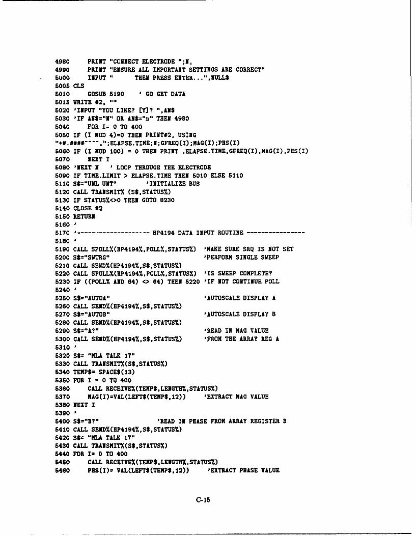
4980 PRINT "CONNECT ELECTRODE ";N,4990 PRINT "ENSURE ALL IMPORTANT SETTINGS ARE CORRECT"5000 INPUT " THEN PRESS E.TER..." ,NULLS6005 CLS5010 GOSUB 6190 ' GO GET DATA
5016 WRITE #2, ""6020 'INPUT "YOU LIKE? [YJ? ",AN$5030 'IF ANS"N" OR ANS="n" THEN 49805040 FOR I= 0 TO 400
6050 IF (I MOD 4)=0 THEN PRINT#2, USING"+#.####...,";ELAPSE.TIME;N;GFREQ(I);AG(I);PHS(I)5060 IF (I MOD 100) = 0 THEN PRINT ,ELAPSE.TIME,GFREQ(I),MAG(I),PHS(I)5070 NEXT I5080 'NEXT N ' LOOP THROUGH THE ELECTRODE5090 IF TIME.LIMIT > ELAPSE.TIME THEN 5010 ELSE 51105110 S$="UNL UNT" 'INITIALIZE BUS5120 CALL TRANSHIT%, (S$,STATUS.)5130 IF STATUS%<>O THEN GOTO 82305140 CLOSE #26150 RETURN5160 16170 '----------- HP4194 DATA INPUT ROUTINE----------------
51805190 CALL SPOLL%(HP4194.,POLL%,STATUS%) 'MAKE SURE SRQ IS NOT SET6200 S$="SWTRG" 'PERFORM SINGLE SWEEP6210 CALL SEND%(HP4194%,.S$,STATUS%)5220 CALL SPOLL%(HP4194,POLL,,STATUS%) 'IS SWEEP COMPLETE?5230 IF ((POLL% AND 64) <> 64) THEN 5220 'IF NOT CONTINUE POLL
5240 15250 S$="AUTOA" 'AUTOSCALE DISPLAY A5260 CALL SEND%(HP4194%,S$,STATUS.)5270 S$="AUTOB" 'AUTOSCALE DISPLAY B6280 CALL SEND% (HP4194%,S$,STATUS%)5290 S$="A?" 'READ IN HAG VALUE5300 CALL SEND%(HP4194%,S$,STATUS%) 'FROM THE ARRAY REG A5310 1
6320 S$= "MLA TALK 17"6330 CALL TRANSMIT%(S$,STATUS%)
6340 TEMP$= SPACES(13)6350 FOR I = 0 TO 4005360 CALL RECEIVE%(TEMPS,LENGTH%,STATUS%)
5370 MAG(I)=VAL(LEFT$(TEMP$,12)) 'EXTRACT MAG VALUE5380 NEXT I6390 15400 S$="B?" 'READ IN PHASE FROM ARRAY REGISTER B6410 CALL SEND%(HP4194%,S$,STATUS%)
5420 S$= "MLA TALK 17"5430 CALL TRANSMIT%(S$,STATUS%)5440 FOR I= 0 TO 4006450 CALL RECEIVEX (TEMPSLENGTH%, STATUS%)6460 PHS(I)= VAL(LEFTS(TEMP$,12)) 'EXTRACT PHASE VALUE
C-15
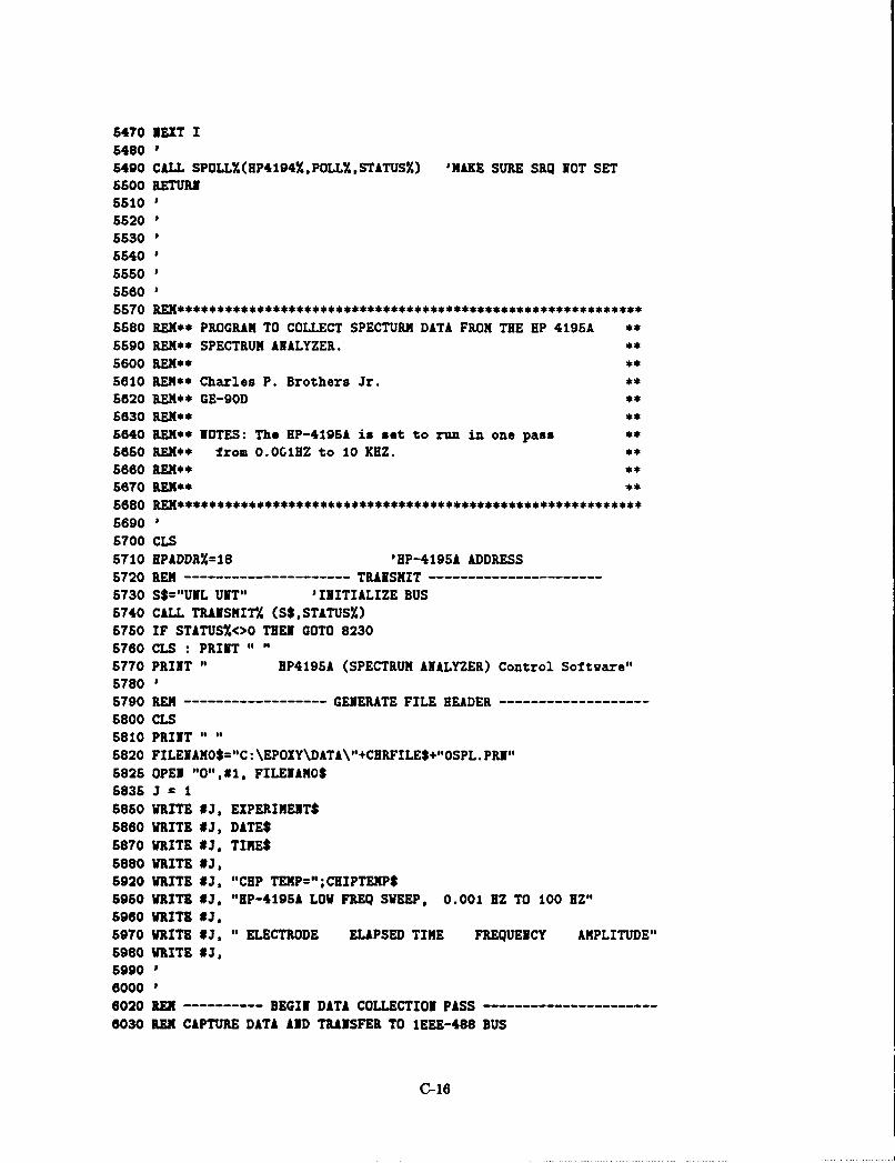
5470 NEXT I5480 '
5490 CALL SPOLL%(HP4194%,POLL%,STATUS%) 'MAKE SURE SRQ NOT SET5500 RETURN651055205530
5640
65605560
5570 RE**********s*************************oooooooooooooooeooo****
5580 REM** PROGRAM TO COLLECT SPECTURM DATA FROM THE HP 4195A **
5590 REM** SPECTRUM ANALYZER. **
5600 REM** **
5610 REM** Charles P. Brothers Jr. **
5620 REM** GE-90D **
5630 REM** **
5640 REM** NOTES: The HP-4195A is set to run in one pass *6650 REM** froam O.OG1HZ to 10 KHZ. *
5660 REM** *
5670 REM** *0
5680 R * * * * * * * * o *o o5690
5700 CLS
5710 HPADDR%=18 'HP-4195A ADDRESS
5720 REM --------------------- TRANSMIT---------------------5730 S$="UNL UNT" 'INITIALIZE BUS
5740 CALL TRANSMIT% (S$,STATUS%)5750 IF STATUS%<>O THEN GOTO 8230
5760 CLS : PRINT " "
5770 PRINT " HP4195A (SPECTRUM ANALYZER) Control Software"5780 1
5790 REM ------------------ GENERATE FILE HEADER------------------5800 CLS
5810 PRINT " "
5820 FILENAMO$="C: \EPOXY\DATA\"+CHRFILE$+"OSPL. PRN'5826 OPEN "0",#1, FILENAMO$5835 J = I
5850 WRITE #J, EXPERIMENTS6860 WRITE #J, DATES
5870 WRITE #J, TIME$
6880 WRITE #3,5920 WRITE #J, "ClP TEMP=";CHIPTEMP$5950 WRITE #J, "HP-4195A LOW FREQ SWEEP, 0.001 HZ TO 100 HZ"6960 WRITE #J,5970 WRITE #J, " ELECTRODE ELAPSED TIME FREQUENCY AMPLITUDE"
5980 WRITE #3,5990
6000
6020 REM ---------- BEGIN DATA COLLECTION PASS---------------------
6030 REM CAPTURE DATA AND TRANSFER TO 1EEE-488 BUS
C-16
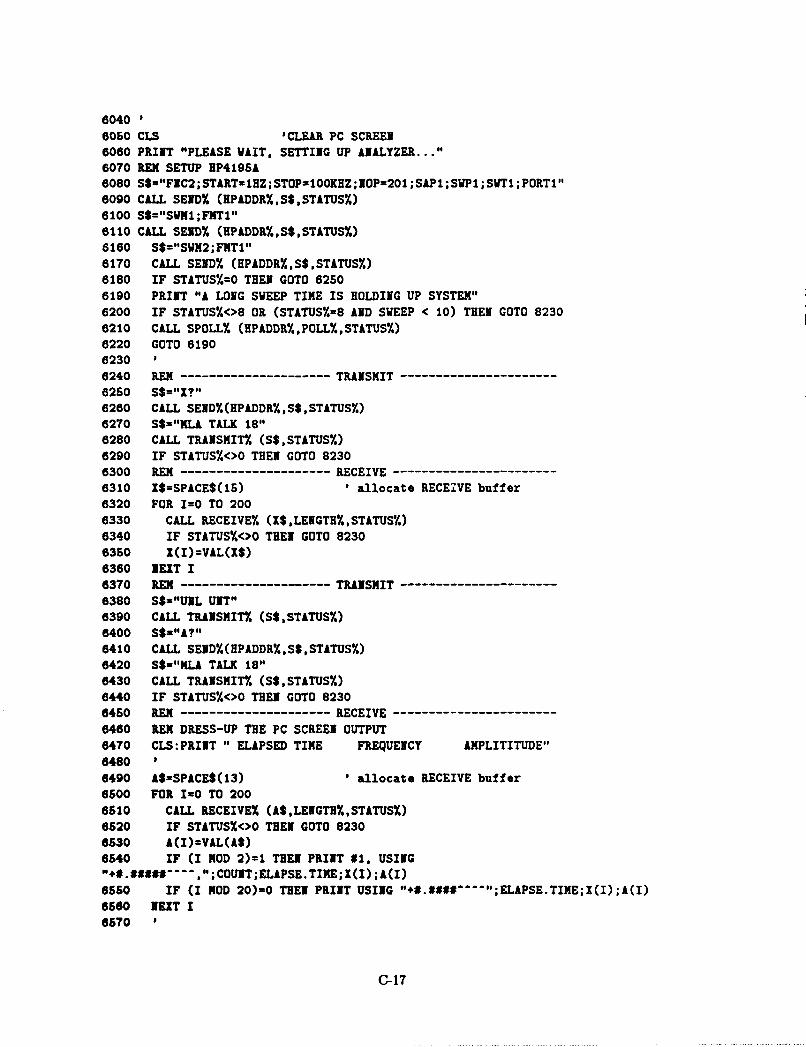
60406060 CLS 'CLEAR PC SCREEN
6060 PRINT "PLEASE WAIT. SETTING UP ANALYZER..."6070 REM SETUP HP4195A6080 S$="FNC2;START=IHZ; STOP=100KHZ;NOP=201 ; SAP1 ; SWP1 ; SWT1 ; PORTI"6090 CALL SEND% (HPADDR%,S$,STATUS%)
6100 S$="SWM1 ;FNT1'6110 CALL SEND% (EPADDR.S,S$,STATUS%)
6160 S$="SWM2;FMTI"6170 CALL SEND% (HPADDR%,S$,STATUS%)6180 IF STATUSS=O THEN GOTO 62506190 PRINT "A LONG SWEEP TIME IS HOLDING UP SYSTEM"
6200 IF STATUSS<>8 OR (STATUSS=8 AND SWEEP < 10) THEN GOTO 8230
6210 CALL SPOLLY. (HPADDRYSPOLL%,,STATUS%)
6220 GOTO 61906230
6240 REM --------------------- TRANSMIT---------------------
6250 S$="X?"6260 CALL SEND%(HPADDRS,S$,STATUSS)6270 S$="M*A TALK 18"6280 CALL TRANSMIT% (S$,STATUS%)6290 IF STATUS%<>O THEN GOTO 82306300 REM --------------------- RECEIVE----------------------
6310 I$=SPACES(15) ' allocate RECEIVE buffer6320 FOR T=O TO 200
6330 CALL RECEIVEY (X$,LENGTH,STATUS'I.)
6340 IF STATUS%<>O THEN GOTO 8230
6350 X(I)=VAL(X$)
6360 NEXT I6370 REX --------------------- TRANSMIT---------------------6380 S$="UNL UNT"6390 CALL TRANSMIT% (S$,STATUS,)6400 S$="A?"6410 CALL SEND%(HPADDRS,S$,STATUS%)
6420 S$="MLA TALK 18"
6430 CALL TRANSMITY/ (S$,STATUS%)6440 IF STATUS%<>O THEN GOTO 82306450 REM --------------------- RECEIVE----------------------6460 REM DRESS-UP THE PC SCREEN OUTPUT6470 CLS: PRINT " ELAPSED TIME FREQUENCY AMPLITITUDE"64806490 AS=SPACE$(13) ' allocate RECEIVE buffer
6600 FOR I=O TO 2006610 CALL RECEIVE% (AS,LENGTH%,STATUS')6620 IF STATUS%<>O THEN GOTO 8230
6630 A(I)=VAL(A$)
6640 IF (I ROD 2)=1 THEN PRINT $1, USING"#. #### ---,,";COUNT;ELAPSE.TIE;X(I);A(I)6550 IF (I ROD 20)=0 THEN PRINT USING "+#.### ---- ";ELAPSE.TIME;I(I);A(I)
6560 NEXT I6570
C-17
6580 S$="SMK1" ' RP-4195L BACK TO CONTINUOUS SWEEP6590 CALL SEND% (HPADDR,S$,STATUS%)6600 IF STATUS%<>O THEN GOTO 82306610 FOR Z = 1 TO 200000!: NEXT Z6612 BEEP: INPUT "TAKE ANOTHER MEASUREMENT? EY] ".AN$6614 IF A$="N" OR AN$="n" THEN 6620 ELSE CLS: GOTO 60206620 CLOSE
6630 PRINT6640 PRINT " DATA TRANSFER COMPLETE."6650 16660 RE --------------------- TRANSMIT---------------------6670 S$="UNL UNT"
6680 CALL TRANSMIT% (S$,STATUS%)
6690 IF STATUS%<>O THEN GOTO 8230
6700 16710 S$="SWM1" ' HP-4195A BACK TO CONTINUOUS SWEEP
6720 CALL SEND% (HPADDRX,S$,STATUS%)
6730 IF STATUS%<>O THEN GOTO 82306740 #
6750 REX ----------- TERMINATE HP-4195A CONTROL---------------6760 S$-"UNL UNT"6770 CALL TRANSMIT% (S$,STATUS%)6780 1
6790 CLS 'CLEAR SCREEN6800 RETURN
6810
6820
6830
6840
68506860 REN*******************************************************
6870 REM** ROUTINE TO COLLECT SPECTURM DATA FROM THE HP 4195A **6880 REM** SPECTRUM ANALYZER. **6890 REM** **
6900 REM** Charles P. Brothers Jr. **
6910 REM** GE-90D **6920 RE.** **
6930 REM** NOTES: The HP-4195A is set to run in one pass
6940 REM** from 0.001HZ to 1.0MHZ.6960 REM**
6960 REM**
6970 J
6980
6990 CLS
7000 HPADDR%=18 'HP-4195A ADDRESS
7010 17020 REM --------------------- TRANSMIT---------------------
7030 S$="UNL UNT" 'INITIALIZE BUS
7040 CALL TRANSMIT% (S$,STATUS%)7050 IF STATUS%<>O TEN GOTO 8230
7060 1
C-18
7070 REM - GENERATE FILE HEADER7080 CLS7090 PRINT " -7100 FILEJAMS = +CHRFILE$+"SPH.PRN"
7110 OPEN "O",1 FILENAMS7120 WRITE *1 FILENAMS7130 WRITE 81. EXPERIMENT$
7140 WRITE 81, DATES7160 WRITE #1, TIMES7160 WRITE *1,7170 WRITE 01, "TEST GAS=";GAS$7180 WRITE 81, "BTU TEMP=";BATE$7190 WRITE 31, "FLW RATE-";FLOWR$
7200 WRITE 81, "CHP TEMP=";CHIPTEMP$7210 WRITE 31, "HUMIDITY=";VHUDS7220 WRITE 1, "7230 WRITE #1, "HP-4196A HIGH FREQ SWEEP, 0.001 HZ TO 1.0 MHZ"7240 WRITE *1,7260 WRITE 31. " ELECTRODE FREQUENCY AMPLITUDE"7260 WRITE #1
7270 '7280 INPUT "ENTER NUMBER OF ELECTRODES TO BE MEASURED: ",ELECT7290 REM ---------- BEGIN DATA COLLECTION PASS7300 REM CAPTURE DATA AND TRANSFER TO IEEE-488 BUS
7310 '7320 CLS 'CLEAR PC SCREEN7330 PRINT "PLEASE WAIT. CAPTURING DATA .
7340 REM SETUP HP4196A7360 SS-"FNC2;START=.OOIHZ;STOP=IMHZ;NOP=401;SAP1;SWP1;SWT1;PORT1;PWRI"
7360 CALL SEND% (HPADDR%.S$,STATUS%)
7370 S$="SVM1;FKTI"7380 CALL SEND% (HPADDR%,S$STATUS%)7390 FOR COUNT = 0 TO (ELECT - 1)7400 PRINT "CONNECT ELECTRODE ";COUNT,
7410 INPUT "HIT RETURN", NULLS7420 INPUT " WAIT FOR DISPLAY TO STABILIZE, HIT RETURN ",NULLS7430 S$="SWM2;FNT1"7440 CALL SENDX (HPADDR%,S$,STATUS%)7460 IF STATUS%"O THEN GOTO 76207460 PRINT "A LONG SWEEP TIME IS HOLDING UP SYSTEM"7470 IF STATUS<>8 OR (STATUS%=8 AND SWEEP < 10) TEEN GOTO 82307480 CALL SPOLL% (HPADDR%,POLLXSTATUS%)
7490 GOTO 74607600 1
7610 RE --------------------- TRANSMIT---------------------7520 S$="l?"
7530 CALL SEND%(HPADDRS$STATUSX)7640 S$="NLA TALK 18"7550 CALL TRANSMIT% (S$,STATUS%)
7560 IF STATUSU<>0 THEEN GOTO 82307670 REM-------------------- RECEIVE----------------------
C- 19
75680 1$=SPACE$(15) ' allocate RECEIVE buffer
7590 FOR I=O TO 4007600 CALL RECEIVE% (X$,LENGTH%,STATUS%)7610 IF STATUS%<>O THEN GOTO 82307620 X(I)=VAL(X$)7630 NEXT I7640 REM --------------------- TRANSMIT---------------------7650 S$='UNL UNT"7660 CALL TRANSMIT% (S$,STATUS%)7670 S$="A?7680 CALL SEND%(HPADDR%,$*,STATUS%)7690 S$="MLA TALK 18"7700 CALL TRANSMITY/ (S$,STATUS%)7710 IF STATUS%<>O THEN GOTO 8230
7720 REM --------------------- RECEIVE----------------------7730 REM DRESS-UP THE PC SCREEN OUTPUT7740 CLS:PRINT " FREQUENCY AMPLITITUDE"7750
7760 AS=SPACE$(13) * allocate RECEIVE buffer7770 FOR I=O TO 4007780 CALL RECEIVE% (A$,LENGTH%,STATUS,)7790 IF STATUS%<>O THEN GOTO 82307800 A(I)=VAL(A$)7810 IF (I MOD 4)=1 THEN PRINT #1, USING "+#.#####..,";COUNT,X(I),A(I)7820 IF (I MOD 40)=0 THEN PRINT X(I);"HZ ";A(I);"dbM"7830 NEXT I78407850 S$="SWM1" HP-4195A BACK TO CONTINUOUS SWEEP
7860 CALL SEND% (HPADDR%,S$,STATUS%)7870 IF STATUS%<>O THEN GOTO 82307880 NEXT COUNT7890 CLOSE #17900 PRINT ""7910 PRINT " DATA TRANSFER TO '";FILENAM$; "' COMPLETE."
7920 1
7930 REM --------------------- TRANSMIT---------------------
7940 S$="UNL UNT"7950 CALL TRANSMIT% (S$,STATUS,)7960 IF STATUS%<>O THEN GOTO 82307970 17980 S$="SWMI" ' HP-4195A BACK TO CONTINUOUS SWEEP
7990 CALL SEND% (HPADDRY.,S$.STATUS%)8000 IF STATUS%<>O THEN GOTO 82308010 1
8020 REM ----------- TERMINATE HP-4195A CONTROL---------------8030 S$="UNL UNT"8040 CALL TRANSMIT% (S$,STATUS%)8050 RETURN
8060
8070
8080
C-20
809081008110 REM ---------- TERMINATE PROGRAM---------81208130 S$='UNL UNT"8140 CALL TRAISMIT%, (SS,STATUS%)8160 CLS 'CLEAR SCREEN8160 SYSTEM817081808190820082108220 REM ------------------- ERR.OR MESSAGE ---------------------8230 PRINT "COMM PROBLEM -- CHECK IEEE-488 CONNECTIONS,8240 PRINT " MAKE SURE EQUIPMENT IS ON AND CONNECTED8250 PRINT " THEN RESTART PROGRA."l8280 STOP8270 REM ------------------- TIMER INITIALIZATION--------82808290 ELAPSE.TIME$"00 :00:00"8300 HOURS = 08310 MINUTES = 08320 SECONDS = 083308340 'TURN ON ELAPSE TIMER83608360 BEGIN.TIME$ =TIME$8371 BEGIN. HRS=VAL(LEFT$ (BEGIN. TIMES. 2))8380 BEGIN.MIN=VAL(MID$(BEGIN.TIME$,4,2))8390 BEGIN. SEC=VAL(RIGHTS (BEGIN .TIME$,2))8400 0N TIMER (1) GOSUB 84408410 TIMER ON8420 RETURN84308440 REXM--------------------TIMER UPDATE-----------84508460 TIME. NOW$=TIME$8470 NOW.HRS = VAL(LEFT$(TIME.NOW$,2))8480 IOW.MIN = VAL(XID$(TIME.NOW$.4,2))8490 IOV.SEC = VAL(RIGHT$(TIME.NOW$,2))8500 SECONDS = VOW.SEC-BEGIN.SEC8510 IF SECONDS >= 0 THEN 85308520 SECONDS=SECONDS+60: NOW.X NIW . IN-18530 MINUTES = NOW.IN-BEGII.XIN8540 IF MINUTES >= 0 THEN 86608560 XINUTES=MINUTES+60: NOW. HRS=NOW.HRS-18660 IF IOW.HRS<BEGIN.HRS THEN NO.HRS=NO.HRS+248570 HOURS a NOV.HRS-BEGIN.HRS8580 IF SECONDS < 10 THEN SECONDS a 11011 + RIGHT*(STR$(SECONDS),1)8590 IF SECONDS >= 10 THEN SECONDS$ x RIGHT$(STR$(SECONDS).2)
0-21
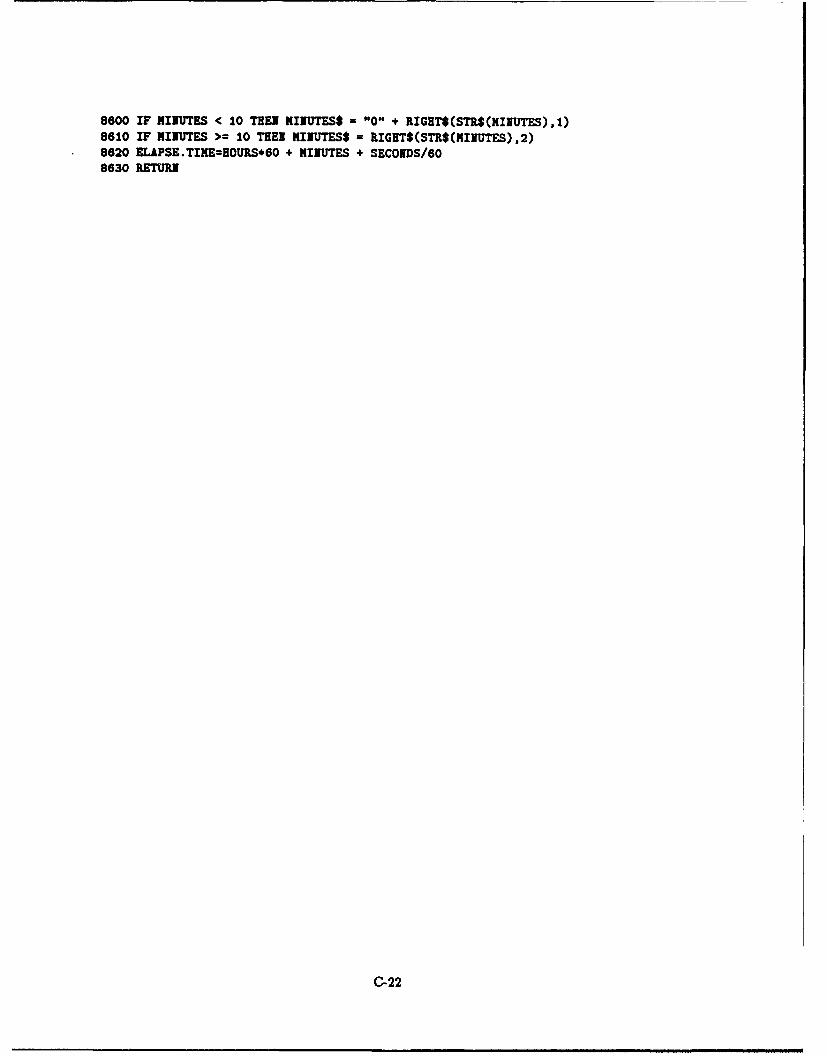
8600 IF MINUTES < 10 THEN MINUTES$ = "0" + RIGBT$(STR$(NINUTES) 51)8610 IF MINUTES >= 10 THEN MINUTES$ = RIGHT$(STR$(XINUTES).2)8620 ELAPSE. TIME=EOURS*60 + MINUTES + SECONDS/608630 RETURN
C-22
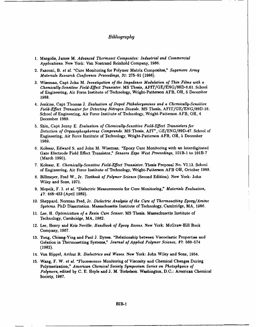
Bibliography
1. Margolis, James M. Advanced Thermoset Composites: Industrial and CommercialApplications. New York: Van Nostrand Reinhold Company, 1986.
2. Fanconi, B. et al. "Cure Monitoring for Polymer Matrix Composites," Sagamore ArmyMaterials Research Conference Proceedings, 31: 275-91 (1986).
3. Wiseman, Capt John M. Investigation of the Impedance Modulation of Thin Films with aChemically-Sensitive Field-Effect Transistor. MS Thesis, AFIT/GE/ENG/88D-6.61. Schoolof Engineering, Air Force Institute of Technology, Wright-Patterson AFB, OH, 5 December1988.
4. Jenkins, Capt Thomas J. Evaluation of Doped Phthalocyanines and a Chemically-SensitiveField-Effect Transistor for Detecting Nitrogen Dioxide. MS Thesis, AFIT/GE/ENG/89D-18.School of Engineering, Air Force Institute of Technology, Wright-Patterson AFB, OH, 4December 1989.
5. Shin, Capt Jenny E. Evaluation of Chemically-Sensitive Field-Effect Transistors forDetection of Organophosphorous Compounds. MS Thesis, AFI"r, GE/ENG/89D-47. School ofEngineering, Air Force Institute of Technology, Wright-Patterson AFB, OH, 5 December1989.
6. Kolesar, Edward S. and John M. Wiseman. "Epoxy Cure Monitoring with an InterdigitatedGate Electrode Field Effect Transistor," Sensors Expo West Proceedings, 101B-1 to 101B-7(March 1990).
7. Kolesar, E. Chemically-Sensitive Field-Effect Transistor. Thesis Proposal No. VI.13. Schoolof Engineering, Air Force Institute of Technology, Wright-Patterson AFB OH, October 1988.
8. Billmeyer, Fred W., Jr. Textbook of Polymer Science (Second Edition). New York: JohnWiley and Sons, 1971.
9. Mopsik, F. I. et al. "Dielectric Measurements for Cure Monitoring," Materials Evaluation,47: 448-453 (April 1989).
10. Sheppard, Norman Fred, Jr. Dielectric Analysis of the Cure of Thermosetting Epoxy/AmineSystems. PhD Dissertation. Massachusetts Institute of Technology, Cambridge, MA, 1986.
11. Lee, H. Optimization of a Resin Cure Sensor. MS Thesis. Massachusetts Institute ofTechnology, Cambridge, MA, 1982.
12. Lee, Henry and Kris Neville. Handbook of Epoxy Resins. New York: McGraw-Hill BookCompany, 1967.
13. Tung, Chiang-Ying and Paul J. Dynes. "Relationship between Viscoelastic Properties andGelation in Thermosetting Systems," Journal of Applied Polymer Science, 27: 569-574(1982).
14. Von Hippel, Arthur R. Dielectrics and Waves. New York: John Wiley and Sons, 1954.
15. Wang, F. W. et al. "Fluorescence Monitoring of Viscosity and Chemical Changes DuringPolymerization," American Chemical Society Symposium Series on Photophysics ofPolymers, edited by C. E. Hoyle and J. M. Torkelson. Washington, D.C.: American ChemicalSociety, 1987.
BIB-I
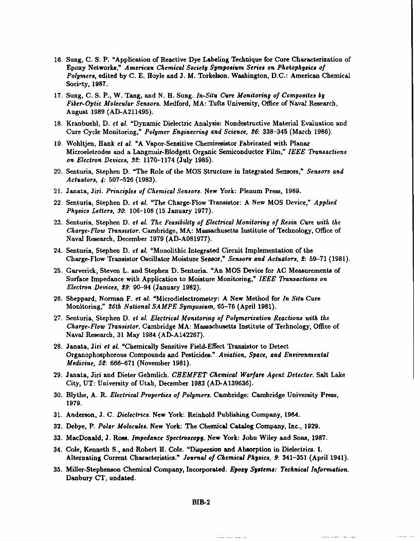
16. Sung, C. S. P. "Application of Reactive Dye Labeling Technique for Cure Characterization ofEpoxy Networks," American Chemical Society Symposium Series on Photophysics ofPolymers, edited by C. E. Hoyle and J. M. Torkelson. Washington, D.C.: American ChemicalSociety, 1987.
17. Sung, C. S. P., W. Tang, and N. H. Sung. In-Situ Cure Monitoring of Composites byFiber-Optic Molecular Sensors. Medford, MA: Tufts University, Office of Naval Research,August 1989 (AD-A211495).
18. Kranbuehl, D. et al. "Dynamic Dielectric Analysis: Nondestructive Material Evaluation andCure Cycle Monitoring," Polymer Engineering and Science, 26: 338-345 (March 1986).
19. Wohltjen, Hank et al. "A Vapor-Sensitive Chemiresistor Fabricated with PlanarMicroeletrodes and a Langmuir-Blodgett Organic Semiconductor Film," IEEE Transactionson Electron Devices, 32: 1170-1174 (July 1985).
20. Senturia, Stephen D. "The Role of the MOS Structure in Integrated Sensors," Sensors andActuators, 4: 507-526 (1983).
21. Janata, Jiri. Principles of Chemical Sensors. New York: Plenum Press, 1989.
22. Senturia, Stephen D. et al. "The Charge-Flow Transistor: A New MOS Device," AppliedPhysics Letters, 30: 106-108 (15 January 1977).
23. Senturia, Stephen D. et al. The Feasibility of Electrical Monitoring of Resin Cure with theCharge-Flow Transistor. Cambridge, MA: Massachusetts Institute of Technology, Office ofNaval Research, December 1979 (AD-A081977).
24. Senturia, Stephen D. et al. "Monolithic Integrated Circuit Implementation of theCharge-Flow Transistor Oscillator Moisture Sensor," Sensors and Actuators, 2: 59-71 (1981).
25. Garverick, Steven L. and Stephen D. Senturia. "An MOS Device for AC Measurements ofSurface Impedance with Application to Moisture Monitoring," IEEE Transactions onElectron Devices, 29: 90-94 (January 1982).
26. Sheppard, Norman F. et al. "Microdielectrometry: A New Method for In Situ CureMonitoring," 26th National SAMPE Symposium, 65-76 (April 1981).
27. Senturia, Stephen D. et al. Electrical Monitoring of Polymerization Reactions with theCharge-Flow Transistor. Cambridge MA: Massachusetts Institute of Technology, Office ofNaval Research, 31 May 1984 (AD-A142267).
28. Janata, Jiri et al. "Chemically Sensitive Field-Effect Transistor to DetectOrganophosphorous Compounds and Pesticides." Aviation, Space, and EnvironmentalMedicine, 52: 666-671 (November 1981).
29. Janata, Jiri and Dieter Gehmlich. CHEMFET Chemical Warfare Agent Detector. Salt LakeCity, UT: University of Utah, December 1983 (AD-A139636).
30. Blythe, A. R. Electrical Properties of Polymers. Cambridge: Cambridge University Press,1979.
31. Anderson, J. C. Dielectrics. New York: Reinhold Publishing Company, 1964.
32. Debye, P. Polar Molecules. New York: The Chemical Catalog Company, Inc., 1929.
33. MacDonald, J. Ross. Impedance Spectroscopy. New York: John Wiley and Sons, 1987.
34. Cole, Kenneth S., and Robert H. Cole. "Dispersion and Absorption in Dielectrics. I.Alternating Current Characteristics." Journal of Chemical Physics, 9. 341-351 (April 1941).
35. Miller-Stephenson Chemical Company, Incorporated. Epozy Systems: Technical Information.Danbury CT, undated.
BIB-2
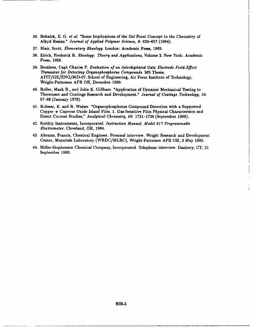
36. Bobalek, E. G. et al. "Some Implications of the Gel Point Concept to the Chemistry ofAlkyd Resins." Journal of Applied Polymer Science, 8: 625-657 (1964).
37. Blair, Scott. Elementary Rheology. London: Academic Press, 1969.
38. Eirich, Frederick R. Rheology: Theory and Applications, Volume 2. New York: AcademicPress, 1958.
39. Brothers, Capt Charles P. Evaluation of an Interdigitated Gate Electrode Field-EffectTransistor for Detecting Organophosphorus Compounds. MS Thesis,AFIT/GE/ENG/90D-07. School of Engineering, Air Force Institute of Technology,Wright-Patterson AFB OH, December 1990.
40. Roller, Mark B., and John K. Gillham. "Application of Dynamic Mechanical Testing toThermoset and Coatings Research and Development." Journal of Coatings Technology, 50:57-68 (January 1978).
41. Kolesar, E. and R. Walser. "Organophosphorus Compound Detection with a SupportedCopper + Cuprous Oxide Island Film. 1. Gas-Sensitive Film Physical Characterisics andDirect Current Studies," Analytical Chemistry, 60: 1731-1736 (September 1988).
42. Keithly Instruments, Incorporated. Instruction Manual, Model 617 ProgrammableElectrometer. Cleveland, OH, 1984.
43. Abrams, Francis, Chemical Engineer. Personal interview. Wright Research and DevelopmentCenter, Materials Laboratory (WRDC/MLBC), Wright-Patterson AFB OH, 3 May 1990.
44. Miller-Stephenson Chemical Company, Incorporated. Telephone interview. Danbury, CT, 21September 1990.
BIB-3
REPORT DOCUMENTATION PAGE Form Approved
I 0MB No. 0704-01885.o~ :-. ~ ec-..c' n!orm.atcn % *st mat"- "u, Der 'eOccse. mc-.orrq trne ,:rn tor revee j~~q n~strruc-i~s. -;ear- es- cata %ourc.<Jjher.q ."I~ i~'.f~ ''e rCeD.,~' ~co~einqarc ~ ~ ~ t.fl t r~-von. ono comments rplarcipg this ourden estimate or inv otrer 4soect: at thi
coce~ton 1 w-t.fl. ' . 64 et-i !:or reou.,n' : r c ~rer *0 .Vasnngton "eacluarers '.e'vices. Z)rectorate for intormation Qoeratiors inct Qeocr-s. 12 i5 jetfeisc,,DaOsH ,. 04. Ar 9on. . :2-42302, 3ra I, - '-e eet'Anaqenment and 3uc3(e' ioer-Ncrk Reac-ron Project 0704-0788). Narjngton. 00 ;3c03
1. AGENCY USE ONLY Leave :Iax 12. REPORT OA 7E REPORT TYPE AND DATES COVERED
7 recerrber 1991 7- MaOster's Thesis4. TITLE AND SUBTITLE 5. FUNDING NUMBERS
EVALJATICtN OF AN IN=~IGITA=D GAME ELECIROE FIELD-EFFECT' TRANSISTOR FOR IN SITU RESIN CURE MILDRINGI
6. AUTHOR(S)
Thares E. Grahar, Captain, USAFI
7. ?EAFCRMING ORGANIZAT:C. AANMEfS) AND ACCIRZ5S(ES) 8. PERFORMING ORGANIZATIONREPORT NUMBER
Air Force Institute of Technology, WPAFB, (]H 45433-6583 AFIT/CE/ENG/91D-55
9. SPONASORING; MCNITCRING AGENCY NAME(S) AND AODRESS(ES) 10. SPONSORING, MONITORING
Wright Laboratory, Materials Directorate (WWL/KBC)AGNYRPT UIE
WPAB CHi 45433-6583
14. SUPPLE.MENTAA ( A07=5S
12a. OISTRIBUTION AVAILABILITY STATEMENT 12b. DISTRIBUTION CODE
Approved for public release; distribution unlimited
l.A ABSTRACT (Maximum 200 words)The purpose of this study was to design an Interdigitated Gate Electrode Field-Effect Transistor (IGEFE) and evaluate its performance as an in situ resin curenriitor. A camrrrcially available resin was selected for the research, andrheological studies were performred to identify the resin's gelation point duringisothermal cures at two selected temperatures. Additional rheological studies wereperformed to identify the resin' s glass transition temperature. The interdigitatedgate electrode of the IGEFETr was coated with samples of the resin, and electricalmeasuremrets were performed while the resin cured. The Chemical changes whichoccur in the resin as a result of curing were manifested in the interdigitatedgate electrode' s electrical characteristics. The results reveal that the IGEFETis capable of sensing the electrical inpedance changes, and hence the chemicalchanges, which occur during the resin's cure. In particular, the chemical changesdue to gelation are evident in the IGEFam's electrical response data. In addition,the resin which was cured at the higher temprature was close to its glasstransition temperature, .-azd hence softer than the resin cured at the lwertenverature, and the IGEFET was capable of detecting this differece.
14. SUBJECT TERMS 15. NUMIiMRf OF PAGESIGEFE, Resin Cure Monitoring, Epoxy, aEMFET, Impedance 209Spectroscop, ~ e - T. (* 16. PRICE CODE
17. SECURITY CLASSIFICATION '18. SECURITY CLASSIFICATION I19. SECURITY CLASSIFICATION 20. LIMITATION OF ABSTRACTOF REPORT OF THIS PAGE I OF ABSTRACT
Unclassified UnlsiiJI Unclassified UL
NSN 7540-01 -280-5500 Standard Form 298 (Rev. 2-89)Priencrbed by ANSI Std Z39.1829-102